Embed Size (px)
Citation preview

TSOP373.., TSOP375..www.vishay.com Vishay Semiconductors
Rev. 2.1, 25-Apr-2018 1 Document Number: 82446
THIS DOCUMENT IS SUBJECT TO CHANGE WITHOUT NOTICE. THE PRODUCTS DESCRIBED HEREIN AND THIS DOCUMENTARE SUBJECT TO SPECIFIC DISCLAIMERS, SET FORTH AT www.vishay.com/doc?91000
IR Receiver Modules for Remote Control Systems
DESIGN SUPPORT TOOLS
ORDERING CODETaping:
TSOP37...TT1 - top view taped
TSOP37...TT2 - top view taped
FEATURES• Very low supply current
• Photo detectors and preamplifier in one package
• Internal filter for PCM frequency
• Supply voltage: 2.5 V to 5.5 V
• Improved immunity against ambient light
• Insensitive to supply voltage ripple and noise
• Material categorization: for definitions of compliance please see www.vishay.com/doc?99912
DESCRIPTIONThe TSOP373.., TSOP375.. series are miniaturized receiver modules for infrared remote control systems. A PIN diode and a preamplifier are assembled on a PCB, the epoxy package contains an IR filter. The demodulated output signal can be directly connected to a microprocessor for decoding.
The TSOP373.. series devices are optimized to suppress almost all spurious pulses from energy saving lamps like CFLs. AGC3 may also suppress some data signals if continuously transmitted.
New designs should prefer the TSOP373.. series containing the newer AGC3. The TSOP375.. series contain a very robust AGC5. This series should only be used for critically noisy environments.
These components have not been qualified according to automotive specifications.
22531-1
click logo to get started
AvailableModels
PARTS TABLE
AGC NOISY ENVIRONMENTSAND SHORT BURSTS (AGC3)
VERY NOISY ENVIRONMENTSAND SHORT BURSTS (AGC5)
Carrier frequency
36 kHz TSOP37336 (1) TSOP37536
38 kHz TSOP37338 (2)(3)(4)(5) TSOP37538
40 kHz TSOP37340 TSOP37540
56 kHz TSOP37356 TSOP37556
Package Belobog
Pinning 1 = OUT, 2, 3, 6, 7, 8 = GND, 4, 5 = VS
Dimensions (mm) 3.95 W x 3.95 H x 0.8 D
Mounting SMD
Application Remote control
Best choice for (1) MCIR (2) Mitsubishi (3) RECS-80 Code (4) r-map (5) XMP-1, XMP-2

TSOP373.., TSOP375..www.vishay.com Vishay Semiconductors
Rev. 2.1, 25-Apr-2018 2 Document Number: 82446
THIS DOCUMENT IS SUBJECT TO CHANGE WITHOUT NOTICE. THE PRODUCTS DESCRIBED HEREIN AND THIS DOCUMENTARE SUBJECT TO SPECIFIC DISCLAIMERS, SET FORTH AT www.vishay.com/doc?91000
BLOCK DIAGRAM APPLICATION CIRCUIT
Note• Stresses beyond those listed under “Absolute Maximum Ratings” may cause permanent damage to the device. This is a stress rating only
and functional operation of the device at these or any other conditions beyond those indicated in the operational sections of this specification is not implied. Exposure to absolute maximum rating conditions for extended periods may affect the device reliability
30 kΩVS
OUTDemo-
GND
passAGCInput
PIN
Banddulator
Control circuit
4, 5
1
2, 3,6, 7, 8
20445-5
C1
IR receiver
GND
Circ
uit
μC
R1
+ VS
GND
Transmitterwith
TSALxxxxVS
VO
17170-11
OUT
R1 and C1 recommended to reduce supply ripple for VS < 2.8 V
ABSOLUTE MAXIMUM RATINGSPARAMETER TEST CONDITION SYMBOL VALUE UNIT
Supply voltage VS -0.3 to +6 V
Supply current IS 3 mA
Output voltage VO -0.3 to (VS + 0.3) V
Output current IO 5 mA
Junction temperature Tj 100 °C
Storage temperature range Tstg -25 to +85 °C
Operating temperature range Tamb -25 to +85 °C
Power consumption Tamb ≤ 85 °C Ptot 10 mW
ELECTRICAL AND OPTICAL CHARACTERISTICS (Tamb = 25 °C, unless otherwise specified)PARAMETER TEST CONDITION SYMBOL MIN. TYP. MAX. UNIT
Supply voltage VS 2.5 - 5.5 V
Supply currentVS = 3.3 V, Ev = 0 ISD 0.27 0.35 0.45 mA
Ev = 40 klx, sunlight ISH - 0.45 - mA
Transmission distance Ev = 0, IR diode TSAL6200, IF = 200 mA, test signal see Fig. 1 d - 45 - m
Output voltage low IOSL = 0.5 mA, Ee = 0.7 mW/m2,test signal see Fig. 1 VOSL - - 100 mV
Minimum irradiancePulse width tolerance:
tpi - 5/fo < tpo < tpi + 6/fo,test signal see Fig. 1
Ee min. - 0.12 0.25 mW/m2
Maximum irradiance tpi - 5/fo < tpo < tpi + 6/fo,test signal see Fig. 1 Ee max. 30 - - W/m2
Directivity Angle of half transmission distance ϕ1/2 - ± 75 - deg

TSOP373.., TSOP375..www.vishay.com Vishay Semiconductors
Rev. 2.1, 25-Apr-2018 3 Document Number: 82446
THIS DOCUMENT IS SUBJECT TO CHANGE WITHOUT NOTICE. THE PRODUCTS DESCRIBED HEREIN AND THIS DOCUMENTARE SUBJECT TO SPECIFIC DISCLAIMERS, SET FORTH AT www.vishay.com/doc?91000
TYPICAL CHARACTERISTICS (Tamb = 25 °C, unless otherwise specified)
Fig. 1 - Output Function
Fig. 2 - Output Pulse Width vs. Irradiance
Fig. 3 - Output Function
Fig. 4 - Output Pulse Diagram
Fig. 5 - Frequency Dependance of Responsivity
Fig. 6 - Sensitivity in Bright Ambient
Ee
T
tpi *)t
VO
VOH
VOL tpo 2) t
14337
Optical Test Signal(IR diode TSAL6200, IF = 0.4 A, N = 6 pulses, f = f0, t = 10 ms)
Output Signal
td 1)
1) 3/f0 < td < 9/f02) tpi - 4/f0 < tpo < tpi + 6/f0
*) tpi ≥ 6/f0 is recommended for optimal function
0
0.05
0.10
0.15
0.20
0.25
0.30
0.35
0.40
0.1 1 10 100 1000 10 000
Ee - Irradiance (mW/m²)
t po -
Out
put P
ulse
Wid
th (
ms)
Input burst length
λ = 950 nm,optical test signal, Fig. 1
Output pulse width
20760
Ee
t
VO
VOH
VOLt
600 µs 600 µs
t = 60 ms
ton toff
94 8134
Optical Test Signal
Output Signal, (see Fig. 4)
0
0.1
0.2
0.3
0.4
0.5
0.6
0.7
0.8
0.1 1 10 100 1000 10 000
Ee - Irradiance (mW/m2)
t on,
t off
- O
utpu
t Pul
se W
idth
(m
s)
20759
λ = 950 nm,optical test signal, Fig. 3
ton
toff
0.0
0.2
0.4
0.6
0.8
1.0
1.2
0.7 0.9 1.1 1.3
f/f0 - Relative Frequency16925
f = f0 ± 5 %
Δf(3 dB) = f0/10
Ee
min
./Ee
- R
elat
ive
Res
pons
ivity
0
0.5
1.0
1.5
2.0
2.5
3.0
3.5
4.0
0.01 0.1 1 10 100
Ee - Ambient DC Irradiance (W/m2)
Ee
min
. - T
hres
hold
Irra
dian
ce (
mW
/m2 ) Correlation with ambient light sources:
10 W/m2 = 1.4 klx (std. illum. A, T = 2855 K)10 W/m2 = 8.2 klx (daylight, T = 5900 K)
Wavelength of ambient illumination: λ = 950 nm
20757

TSOP373.., TSOP375..www.vishay.com Vishay Semiconductors
Rev. 2.1, 25-Apr-2018 4 Document Number: 82446
THIS DOCUMENT IS SUBJECT TO CHANGE WITHOUT NOTICE. THE PRODUCTS DESCRIBED HEREIN AND THIS DOCUMENTARE SUBJECT TO SPECIFIC DISCLAIMERS, SET FORTH AT www.vishay.com/doc?91000
Fig. 7 - Sensitivity vs. Supply Voltage Disturbances
Fig. 8 - Max. Envelope Duty Cycle vs. Burst Length
Fig. 9 - Sensitivity vs. Ambient Temperature
Fig. 10 - Relative Spectral Sensitivity vs. Wavelength
Fig. 11 - Directivity
Fig. 12 - Sensitivity vs. Supply Voltage
0
0.1
0.2
0.3
0.4
0.5
0.6
0.7
0.8
0.9
1.0
1 10 100 1000
VsRMS - AC Voltage on DC Supply Voltage (mV)20753
Ee
min
. - T
hres
hold
Irra
dian
ce (
mW
/m2 )
f = fo
f = 20 kHz
f = 30 kHz
f = 100 Hz
f = 10 kHz
0
0.1
0.2
0.3
0.4
0.5
0.6
0.7
0.8
0.9
1.0
0 20 40 60 80 100 120
Burst Length (number of cycles/burst)
Max
. Env
elop
e D
uty
Cyc
le f = 38 kHz, Ee = 2 mW/m²
TSOP375..
TSOP373..
0
0.05
0.10
0.15
0.20
0.25
0.30
-30 -10 10 30 50 70 90Ee
min
. - T
hres
hold
Irra
dia
nce
(mW
/m2 )
Tamb - Ambient Temperature (°C)
0
0.1
0.2
0.3
0.4
0.5
0.6
0.7
0.8
0.9
1.0
750 800 850 900 950 1000 1050 1150
λ - Wavelength (nm)
S(λ
) rel
- R
elat
ive
Spe
ctra
l Sen
sitiv
ity
1100
Axis Title
2nd
line
2nd
line
2nd
line
Ver
tical
drel. - Relative Transmission Distance
1.0
0.9
0.7
0.8
30°
50°
40°
80°
0.6 0.4 0.20 0.40.2 0.6
20°10°0°
60°
70°
21947
0.00
0.05
0.10
0.15
0.20
0.25
0.30
1 2 3 4 5
Ee
min
. - S
ensi
tivity
(mW
/m2 )
VS - Supply Voltage (V)

TSOP373.., TSOP375..www.vishay.com Vishay Semiconductors
Rev. 2.1, 25-Apr-2018 5 Document Number: 82446
THIS DOCUMENT IS SUBJECT TO CHANGE WITHOUT NOTICE. THE PRODUCTS DESCRIBED HEREIN AND THIS DOCUMENTARE SUBJECT TO SPECIFIC DISCLAIMERS, SET FORTH AT www.vishay.com/doc?91000
SUITABLE DATA FORMATThe TSOP373.., TSOP375.. series is designed to suppress spurious output pulses due to noise or disturbance signals. The devices can distinguish data signals from noise due to differences in frequency, burst length, and envelope duty cycle. The data signal should be close to the device’s band-pass center frequency (e.g. 38 kHz) and fulfill the conditions in the table below.
When a data signal is applied to the TSOP373.., TSOP375.. in the presence of a disturbance, the sensitivity of the receiver is automatically reduced by the AGC to insure that no spurious pulses are present at the receiver’s output. Some examples which are suppressed are:
• DC light (e.g. from tungsten bulbs sunlight)
• Continuous signals at any frequency
• Strongly or weakly modulated patterns from fluorescent lamps with electronic ballasts (see Fig. 13 or Fig. 14)
Fig. 13 - IR Signal from Fluorescent LampWith Low Modulation
Fig. 14 - IR Signal from Fluorescent LampWith High Modulation
Note• For data formats with long bursts (more than 10 carrier cycles) please see the datasheet for TSOP372.., TSOP374..
16920
10
100
1000
10000
0
1
2
3
4
5
6
7
0 5 10 15 20
Axis Title
1st l
ine
2nd
line
2nd
line
IR S
igna
l Am
plitu
de
Time (ms)
16921
10
100
1000
10000
-60
-40
-20
0
20
40
0 5 10 15 20
Axis Title
1st l
ine
2nd
line
2nd
line
IR S
igna
l Am
plitu
de
Time (ms)
TSOP373.. TSOP375..
Minimum burst length 6 cycles/burst 6 cycles/burst
After each burst of length a minimum gap time is required of
6 to 35 cycles≥ 10 cycles
6 to 24 cycles≥ 10 cycles
For bursts greater than a minimum gap time in the data stream is needed of
35 cycles
> 6 x burst length
24 cycles
> 25 ms
Maximum number of continuous short bursts/second 2000 2000
MCIR code Preferred Yes
RCMM code Preferred Yes
XMP-1, XMP-2 code Preferred Yes
Suppression of interference from fluorescent lampsMild and complex disturbance
patterns are suppressed (example:signal pattern of Fig. 13 and 14)
Critical disturbancepatterns are suppressed,e.g. highly dimmed LCDs

TSOP373.., TSOP375..www.vishay.com Vishay Semiconductors
Rev. 2.1, 25-Apr-2018 6 Document Number: 82446
THIS DOCUMENT IS SUBJECT TO CHANGE WITHOUT NOTICE. THE PRODUCTS DESCRIBED HEREIN AND THIS DOCUMENTARE SUBJECT TO SPECIFIC DISCLAIMERS, SET FORTH AT www.vishay.com/doc?91000
PACKAGE DIMENSIONS in millimeters
Notes(1) Optically effective area(2) Pins connected internally. It is not necessary to connect externally
Drawing-No.: 6.550-5315.01-4Issue: 2; 12.02.14
Not indicated tolerances ± 0.1
technical drawingsaccording to DIN
specifications
Proposed pad layout fromcomponent side
(dim. for reference only)
(3.95)
(3.9
5)
(0.35)
(0.8
)
(2.7
5)
(3)
(4 x)
(4x)
0.55
(0.9
5)
0.55
(1.8
)
0.75± 0.05
4 x 0.75 = 3
0.35± 0.05
(8 x)
1.5
3
(0.3
)
(0.3
) (0.3)
(0.7
)
0.475
(0.4
)
0.8
0.15
Pinning from topview
GN
D
GN
D
Out
Vs
(Vs)
(GN
D)
(GN
D)
(GN
D)
1 2 3 4 5
8 7 6
Pin 1 identification
(2)
(2) (2) (2)
3.95
3.95
(2.7
5)
(1.9
)
(3.4)
marking areaPin 1 Identification
(1)
(1)
(1)

TSOP373.., TSOP375..www.vishay.com Vishay Semiconductors
Rev. 2.1, 25-Apr-2018 7 Document Number: 82446
THIS DOCUMENT IS SUBJECT TO CHANGE WITHOUT NOTICE. THE PRODUCTS DESCRIBED HEREIN AND THIS DOCUMENTARE SUBJECT TO SPECIFIC DISCLAIMERS, SET FORTH AT www.vishay.com/doc?91000
ASSEMBLY INSTRUCTIONSReflow Soldering
• Reflow soldering must be done within 168 h while stored under a max. temperature of 30 °C, 60 % RH after opening the dry pack envelope
• Set the furnace temperatures for pre-heating and heating in accordance with the reflow temperature profile as shown in the diagram. Exercise extreme care to keep the maximum temperature below 260 °C. The temperature shown in the profile means the temperature at the device surface. Since there is a temperature difference between the component and the circuit board, it should be verified that the temperature of the device is accurately being measured
• Handling after reflow should be done only after the work surface has been cooled off
Manual Soldering
• Use a soldering iron of 25 W or less. Adjust the temperature of the soldering iron below 300 °C
• Finish soldering within 3 s
• Handle products only after the temperature has cooled off
VISHAY LEAD (Pb)-FREE REFLOW SOLDER PROFILE
Note(1) MOQ: minimum order quantity
ORDERING INFORMATIONORDERING CODE PACKAGING VOLUME (1) REMARKS
TSOP37..TT1Tape and reel
MOQ: 1800 pcs3.95 mm x 3.95 mm x 0.75 mm
TSOP37..TT2 MOQ: 7000 pcs
max. 120 s max. 100 s
max. 20 s
Max. ramp up 3 °C/s
max. 260 °C
10
100
1000
10000
0
50
100
250
300
0 300
Axis Title
2nd
line
Tem
pera
ture
(°C
)
Time (s)25020015010050
200
150
245 °C
217 °C240 °C255 °C
Max. ramp down 6 °C/s
Max. 2 cycles allowed
19800

TSOP373.., TSOP375..www.vishay.com Vishay Semiconductors
Rev. 2.1, 25-Apr-2018 8 Document Number: 82446
THIS DOCUMENT IS SUBJECT TO CHANGE WITHOUT NOTICE. THE PRODUCTS DESCRIBED HEREIN AND THIS DOCUMENTARE SUBJECT TO SPECIFIC DISCLAIMERS, SET FORTH AT www.vishay.com/doc?91000
TAPING VERSION TSOP37... DIMENSIONS in millimeters
Parts mounted
Empty trailer 200 mm min.
Empty leader 400 mm min.
Direction of pulling out
Ø 6
0 m
in.
Ø Y
2 ± 0.5
Label posted here
coming out from reelTape position
(12.4)
18.4 max.
Ø 13 ± 0.2Ø 21 ± 0.8
100 mm min. with cover tape
X 2:1
(2) (1.7
5)
(5.5
)
12 ±
0.3
(8) (4)(Ø 1.5)
(0.3)
(1.2)
Technical drawingsaccording to DINspecifications
Not indicated tolerances ± 0.1Drawing-No.: 9.700-5347.01-4Issue: 2; 07.03.18
TT1 Ø 180 ± 2 = 1800 pcs.
Leader and trailer tape:

TSOP373.., TSOP375..www.vishay.com Vishay Semiconductors
Rev. 2.1, 25-Apr-2018 9 Document Number: 82446
THIS DOCUMENT IS SUBJECT TO CHANGE WITHOUT NOTICE. THE PRODUCTS DESCRIBED HEREIN AND THIS DOCUMENTARE SUBJECT TO SPECIFIC DISCLAIMERS, SET FORTH AT www.vishay.com/doc?91000
LABELStandard bar code labels for finished goods
The standard bar code labels are product labels and used for identification of goods. The finished goods are packed in final packing area. The standard packing units are labeled
with standard bar code labels before transported as finished goods to warehouses. The labels are on each packing unit and contain Vishay Semiconductor GmbH specific data.
DRY PACKINGThe reel is packed in an anti-humidity bag to protect the devices from absorbing moisture during transportation and storage.
FINAL PACKINGThe sealed reel is packed into a cardboard box.
RECOMMENDED METHOD OF STORAGEDry box storage is recommended as soon as the aluminum bag has been opened to prevent moisture absorption. The following conditions should be observed, if dry boxes are not available:
• Storage temperature 10 °C to 30 °C
• Storage humidity ≤ 60 % RH max.
After more than 168 h under these conditions moisture content will be too high for reflow soldering.
In case of moisture absorption, the devices will recover to the former condition by drying under the following condition:
192 h at 40 °C + 5 °C / - 0 °C and < 5 % RH (dry air / nitrogen) or
96 h at 60 °C + 5 °C and < 5 % RH for all device containers or
24 h at 125 °C + 5 °C not suitable for reel or tubes.
An EIA JEDEC® standard J-STD-020 level 3 label is included on all dry bags.
VISHAY SEMICONDUCTOR GmbH STANDARD BAR CODE PRODUCT LABEL (finished goods)PLAIN WRITING ABBREVIATION LENGTH
Item-description - 18
Item-number INO 8
Selection-code SEL 3
LOT-/serial-number BATCH 10
Data-code COD 3 (YWW)
Plant-code PTC 2
Quantity QTY 8
Accepted by ACC -
Packed by PCK -
Mixed code indicator MIXED CODE -
Origin xxxxxxx+ Company logo
Long bar code top Type Length
Item-number N 8
Plant-code N 2
Sequence-number X 3
Quantity N 8
Total length - 21
Short bar code bottom Type Length
Selection-code X 3
Data-code N 3
Batch-number X 10
Filter - 1
Total length - 17
Aluminum bag
Label
Reel
15973

TSOP373.., TSOP375..www.vishay.com Vishay Semiconductors
Rev. 2.1, 25-Apr-2018 10 Document Number: 82446
THIS DOCUMENT IS SUBJECT TO CHANGE WITHOUT NOTICE. THE PRODUCTS DESCRIBED HEREIN AND THIS DOCUMENTARE SUBJECT TO SPECIFIC DISCLAIMERS, SET FORTH AT www.vishay.com/doc?91000
EIA JEDC standard J-STD-020 level 3 label is included on all dry bags
ESD PRECAUTIONProper storage and handling procedures should be followed to prevent ESD damage to the devices especially when they are removed from the antistatic shielding bag. Electrostatic sensitive devices warning labels are on the packaging.
VISHAY SEMICONDUCTORS STANDARD BAR CODE LABELSThe Vishay Semiconductors standard bar code labels are printed at final packing areas. The labels are on each packing unit and contain Vishay Semiconductors specific data.
BAR CODE PRODUCT LABEL (example)
1. Calculated shelf life in sealed bag: 12 months at <40°C and <90% relative humidity (RH)
3. After bag is opened, devices that will be subjected to reflow solder or other high temperature process must be
4. Devices require bake, before mounting, if:
a) Humidity Indicator Card reads > 10% for level 2a - 5a devices or >60% for level 2 devices when read at 23±5°C
b) 3a or 3b are not met
5. If baking is required, refer to IPC/JEDEC J-STD-033 for bake procedure
2. Peak package body temperature:_______________________°CIf blank, see adjacent bar code label
a) Mounted within:___________________hours of factory conditions
≤30°C/60% RH, or b) Stored per J-STD-033
If blank, see adjacent bar code label
Bag Seal Date:_________________________________________If blank, see adjacent bar code label
Note: Level and body temperature defined by IPC/JEDEC J-STD-020
This bag containsMOISTURE-SENSITIVE DEVICES
CautionIf blank, see adjacent
bar code label
3LEVEL
260
168
22650
22178

SMD Tape and Reelwww.vishay.com Vishay Semiconductors
Rev. 2.5, 08-Mar-18 1 Document Number: 80125
THIS DOCUMENT IS SUBJECT TO CHANGE WITHOUT NOTICE. THE PRODUCTS DESCRIBED HEREIN AND THIS DOCUMENTARE SUBJECT TO SPECIFIC DISCLAIMERS, SET FORTH AT www.vishay.com/doc?91000
Tape and Reel Standards for Surface-Mount IR Receiver ModulesVishay Semiconductor surface-mount IR receivers are packaged on tape and reel. The following specification is based on IEC publication 286, which takes the industrial requirements for automatic insertion into account.
Absolute maximum ratings, mechanical dimensions, optical and electrical characteristics for taped devices are identical to the basic catalog types and can be found in the specifications for untaped devices.
PACKAGINGThe tapes of components are available on reels. Each reel is marked with labels which contain the following information:
- Vishay
- Type
- Group
- Tape code, normally part of type name
- Production code
- Quantity
MISSING COMPONENTSUp to 3 consecutive components may be missing if the gap is followed by at least 6 components. A maximum of 0.5 % of the components per reel quantity may be missing. At least 5 empty positions are present at the start and the end of the tape to enable tape insertion.
Tensile strength of the tape: > 15 N
NUMBER OF COMPONENTSA. Panhead: quantity per reel:
TT, top view package, 1190 pcs
TR, side view package, 1120 pcs
B. Heimdall: quantity per reel:
TT, top view package, 2200 pcs
TR, side view package, 2300 pcs
C. Heimdall without lens: quantity per reel:
WTT, top view package, 2200 pcs
WTR, side view package, 2300 pcs
D. Belobog: quantity per reel:
TT1, top view package, 1800 pcs
E. Belobog with shield: quantity per reel:
TT1, top view package, 1500 pcs
F. Minimold DF1P: quantity per reel:
DF1P, 1100 pcs
G. TVCastSMD TR1: quantity per reel:
TR1, side view package, 2000 pcs
ORDER DESIGNATIONThe type designation of the device is extended by TT or TT1 for top view or TR for side view.
Example:
TSOP6238TR (reel packing)
TSOP75238TR (reel packing)
TSOP75338WTT (reel packing)
TSOP57438TT1 (reel packing)
TSOP57238HTT1 (reel packing)
TSOP39438TR1 (reel packing)

SMD Tape and Reelwww.vishay.com Vishay Semiconductors
Rev. 2.5, 08-Mar-18 2 Document Number: 80125
THIS DOCUMENT IS SUBJECT TO CHANGE WITHOUT NOTICE. THE PRODUCTS DESCRIBED HEREIN AND THIS DOCUMENTARE SUBJECT TO SPECIFIC DISCLAIMERS, SET FORTH AT www.vishay.com/doc?91000
REEL DIMENSIONS FOR PANHEAD, HEIMDALL, AND TVCASTSMD TR in millimeters
Note• The body structure of the reel can vary
16734
SMD Tape and Reelwww.vishay.com Vishay Semiconductors
Rev. 2.5, 08-Mar-18 3 Document Number: 80125
THIS DOCUMENT IS SUBJECT TO CHANGE WITHOUT NOTICE. THE PRODUCTS DESCRIBED HEREIN AND THIS DOCUMENTARE SUBJECT TO SPECIFIC DISCLAIMERS, SET FORTH AT www.vishay.com/doc?91000
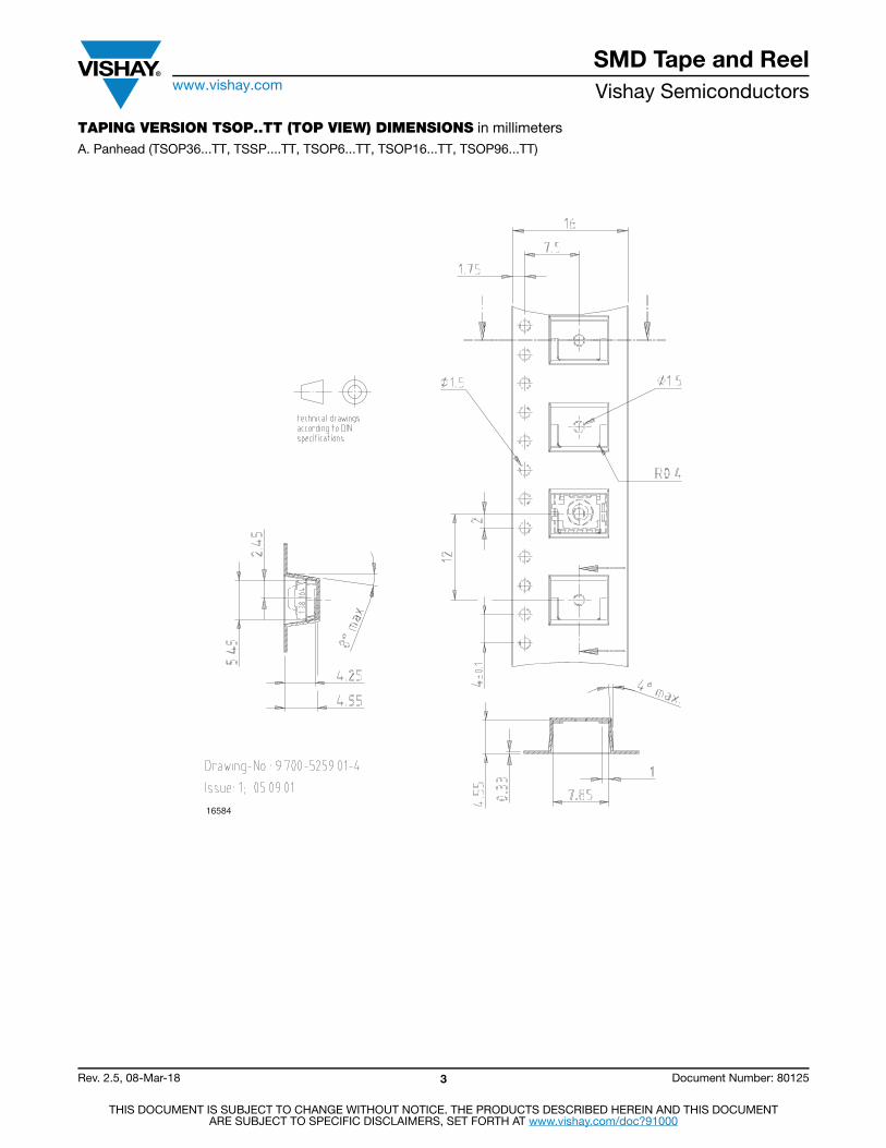
TAPING VERSION TSOP..TT (TOP VIEW) DIMENSIONS in millimetersA. Panhead (TSOP36...TT, TSSP....TT, TSOP6...TT, TSOP16...TT, TSOP96...TT)
16584

SMD Tape and Reelwww.vishay.com Vishay Semiconductors
Rev. 2.5, 08-Mar-18 4 Document Number: 80125
THIS DOCUMENT IS SUBJECT TO CHANGE WITHOUT NOTICE. THE PRODUCTS DESCRIBED HEREIN AND THIS DOCUMENTARE SUBJECT TO SPECIFIC DISCLAIMERS, SET FORTH AT www.vishay.com/doc?91000
TAPING VERSION TSOP..TT (TOP VIEW) DIMENSIONS in millimetersB. Heimdall (TSOP75...TT, TSOP77...TT, TSSP77...TT, TSOP15...TT, TSOP95...TT)
0.3
3.65
16
7.51.75
Ø 1.5
Ø 1.5
2
84
Drawing-No.: 9.700-5338.01-4Issue: 4; 12.06.13
technical drawingsaccording to DINspecifications
Dire
ctio
n of
feed

SMD Tape and Reelwww.vishay.com Vishay Semiconductors
Rev. 2.5, 08-Mar-18 5 Document Number: 80125
THIS DOCUMENT IS SUBJECT TO CHANGE WITHOUT NOTICE. THE PRODUCTS DESCRIBED HEREIN AND THIS DOCUMENTARE SUBJECT TO SPECIFIC DISCLAIMERS, SET FORTH AT www.vishay.com/doc?91000
TAPING VERSION TSOP..TT (TOP VIEW) DIMENSIONS in millimetersC. Heimdall without lens (TSOP75...WTT, TSOP77...WTT, TSSP77...WTT, TSOP15...WTT, TSOP95...WTT)
2
1.75 7.5
16
8
4
30.3
Ø 1.5 min.
Ø 1.5
Drawing-No.: 9.700-5341.01-4Issue: 3; 06.10.15
technical drawingsaccording to DINspecifications
Dire
ctio
n of
feed

SMD Tape and Reelwww.vishay.com Vishay Semiconductors
Rev. 2.5, 08-Mar-18 6 Document Number: 80125
THIS DOCUMENT IS SUBJECT TO CHANGE WITHOUT NOTICE. THE PRODUCTS DESCRIBED HEREIN AND THIS DOCUMENTARE SUBJECT TO SPECIFIC DISCLAIMERS, SET FORTH AT www.vishay.com/doc?91000
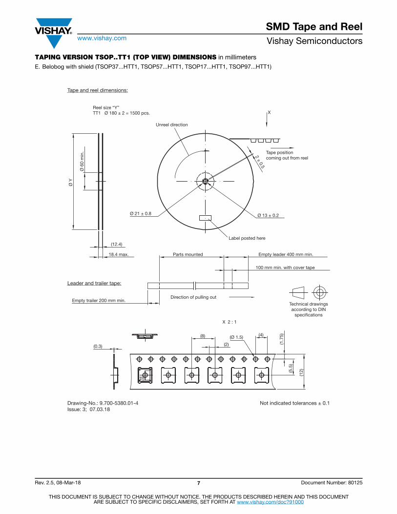
TAPING VERSION TSOP..TT1 (TOP VIEW) DIMENSIONS in millimetersD. Belobog (TSOP37...TT1, TSOP57...TT1, TSOP17...TT1, TSOP97...TT1)
Tape and reel dimensions:
Parts mounted
Empty trailer 200 mm min.
Empty leader 400 mm min.
Direction of pulling out
Unreel direction
Ø 6
0 m
in.
Ø Y
2 ± 0.5
Label posted here
coming out from reelTape position
(12.4)
18.4 max.
Ø 13 ± 0.2Ø 21 ± 0.8
100 mm min. with cover tape
X 2:1
(2) (1.7
5)
(5.5
)
12 ±
0.3
(8) (4)(Ø 1.5)
(0.3)
(1.2)
Technical drawingsaccording to DINspecifications
Not indicated tolerances ± 0.1Drawing-No.: 9.700-5347.01-4Issue: 2; 07.03.18
Reel size “Y”TT1 Ø 180 ± 2 = 1800 pcs.
Leader and trailer tape:
SMD Tape and Reelwww.vishay.com Vishay Semiconductors
Rev. 2.5, 08-Mar-18 7 Document Number: 80125
THIS DOCUMENT IS SUBJECT TO CHANGE WITHOUT NOTICE. THE PRODUCTS DESCRIBED HEREIN AND THIS DOCUMENTARE SUBJECT TO SPECIFIC DISCLAIMERS, SET FORTH AT www.vishay.com/doc?91000
TAPING VERSION TSOP..TT1 (TOP VIEW) DIMENSIONS in millimetersE. Belobog with shield (TSOP37...HTT1, TSOP57...HTT1, TSOP17...HTT1, TSOP97...HTT1)
Reel size “Y”TT1 Ø 180 ± 2 = 1500 pcs.
Unreel direction
X
Tape positioncoming out from reel
2 ± 0.5
Ø 13 ± 0.2Ø 21 ± 0.8
Label posted here
Ø Y
Ø 6
0 m
in.
18.4 max.
(12.4)
Parts mounted Empty leader 400 mm min.
100 mm min. with cover tape
Direction of pulling outEmpty trailer 200 mm min.
X 2 : 1
(8)
(2)
(4)(Ø 1.5)
(1.7
5)
(0.3)
(5.5
)
(12)
Technical drawingsaccording to DINspecifications
Drawing-No.: 9.700-5380.01-4Issue: 3; 07.03.18
Not indicated tolerances ± 0.1
Tape and reel dimensions:
Leader and trailer tape:

SMD Tape and Reelwww.vishay.com Vishay Semiconductors
Rev. 2.5, 08-Mar-18 8 Document Number: 80125
THIS DOCUMENT IS SUBJECT TO CHANGE WITHOUT NOTICE. THE PRODUCTS DESCRIBED HEREIN AND THIS DOCUMENTARE SUBJECT TO SPECIFIC DISCLAIMERS, SET FORTH AT www.vishay.com/doc?91000
TAPING VERSION TSOP..DF1P (SIDE VIEW) DIMENSIONS in millimetersF. Minimold DF1P (TSOP33...DF1P, TSOP53...DF1P, TSOP13...DF1P, TSOP93...DF1P)
Drawing-No.: 9.800-5052.V3-4Issue: 1; 17.12.02
Form of the leave open of the wheel is supplier specific.Dimensions according to IEC EN 60 286-3
Tape width: 24
Technical drawingaccording to DINspecifications
Reel hub 2:1
Ø 20.2 min.
1.5
min
.
Ø 1
2.8
min
.
Ø 6
0 m
in.
24.4 +3
-0
Ø 3
30 +
0 -4
Drawing-No.: 9.700-5399.01-4Issue: 1; 30.06.16 (6.08)
(1.5 min.) (12)
(1.7
5)
(11.
5)
(24)
(2)(4) (1.55) (0.4)
(5.25)
(11.
75)
B
BAA B - B
A - A

SMD Tape and Reelwww.vishay.com Vishay Semiconductors
Rev. 2.5, 08-Mar-18 9 Document Number: 80125
THIS DOCUMENT IS SUBJECT TO CHANGE WITHOUT NOTICE. THE PRODUCTS DESCRIBED HEREIN AND THIS DOCUMENTARE SUBJECT TO SPECIFIC DISCLAIMERS, SET FORTH AT www.vishay.com/doc?91000
TAPING VERSION TSOP..TR (SIDE VIEW) DIMENSIONS in millimetersG. TVCastSMD TR1 (TSOP59...TR1, TSOP39...TR1, TSOP19...TR1, TSOP99...TR1)
A-A (2 : 1)
B-B (2 : 1)
A A
B
B
Dire
ctio
n of
feed
(1.75)(7.5)
(16)
(Ø 1)
(2)
(12)
(4)
Ø 1.5
(9.75)
(2.8
5)
(7.0
5)
1.7
()
Technical drawingsaccording to DINspecification.
Drawing-No.: GO-100220.10_ZIssue B: 08.02.17
SMD Tape and Reelwww.vishay.com Vishay Semiconductors
Rev. 2.5, 08-Mar-18 10 Document Number: 80125
THIS DOCUMENT IS SUBJECT TO CHANGE WITHOUT NOTICE. THE PRODUCTS DESCRIBED HEREIN AND THIS DOCUMENTARE SUBJECT TO SPECIFIC DISCLAIMERS, SET FORTH AT www.vishay.com/doc?91000
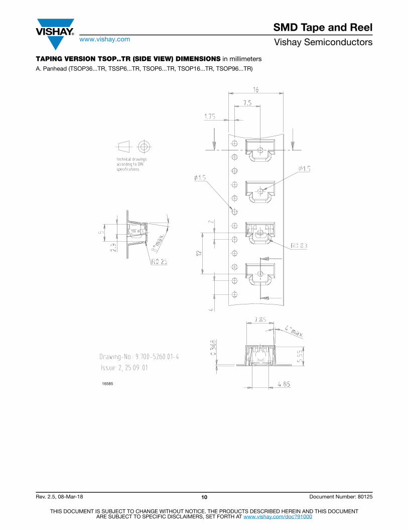
TAPING VERSION TSOP..TR (SIDE VIEW) DIMENSIONS in millimetersA. Panhead (TSOP36...TR, TSSP6...TR, TSOP6...TR, TSOP16...TR, TSOP96...TR)
16585
SMD Tape and Reelwww.vishay.com Vishay Semiconductors
Rev. 2.5, 08-Mar-18 11 Document Number: 80125
THIS DOCUMENT IS SUBJECT TO CHANGE WITHOUT NOTICE. THE PRODUCTS DESCRIBED HEREIN AND THIS DOCUMENTARE SUBJECT TO SPECIFIC DISCLAIMERS, SET FORTH AT www.vishay.com/doc?91000
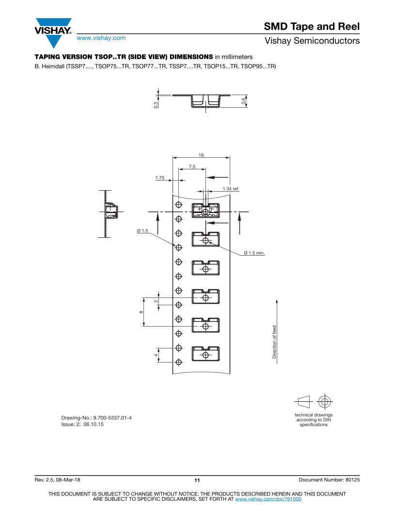
TAPING VERSION TSOP..TR (SIDE VIEW) DIMENSIONS in millimetersB. Heimdall (TSSP7...., TSOP75...TR, TSOP77...TR, TSSP7....TR, TSOP15...TR, TSOP95...TR)
Drawing-No.: 9.700-5337.01-4Issue: 2; 06.10.15
2
1.75
7.5
16
8
4
3.6
0.3
Ø 1.5 min.
Ø 1.5
Dire
ctio
n of
feed
1.34 ref.
technical drawingsaccording to DINspecifications
SMD Tape and Reelwww.vishay.com Vishay Semiconductors
Rev. 2.5, 08-Mar-18 12 Document Number: 80125
THIS DOCUMENT IS SUBJECT TO CHANGE WITHOUT NOTICE. THE PRODUCTS DESCRIBED HEREIN AND THIS DOCUMENTARE SUBJECT TO SPECIFIC DISCLAIMERS, SET FORTH AT www.vishay.com/doc?91000
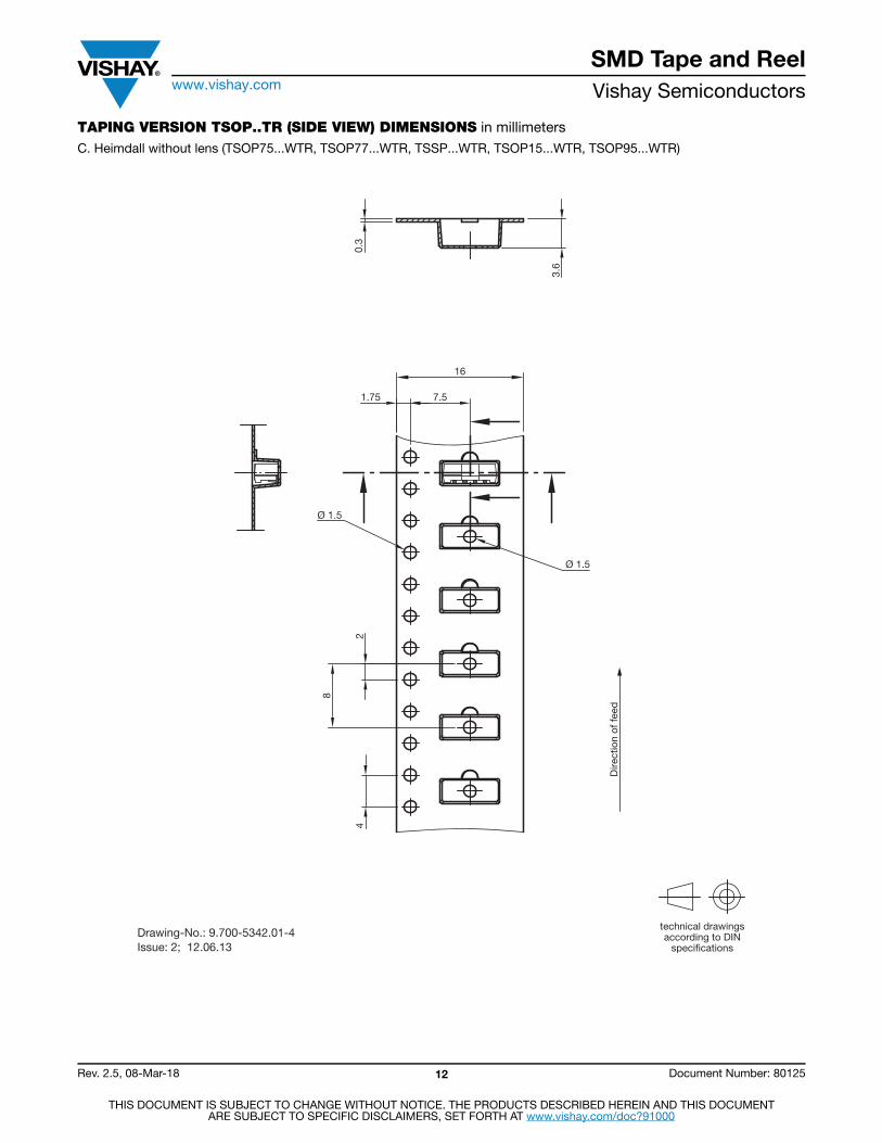
TAPING VERSION TSOP..TR (SIDE VIEW) DIMENSIONS in millimetersC. Heimdall without lens (TSOP75...WTR, TSOP77...WTR, TSSP...WTR, TSOP15...WTR, TSOP95...WTR)
2
1.75 7.5
16
8
4
3.6
0.3
Ø 1.5
Ø 1.5
Drawing-No.: 9.700-5342.01-4Issue: 2; 12.06.13
technical drawingsaccording to DINspecifications
Dire
ctio
n of
feed
SMD Tape and Reelwww.vishay.com Vishay Semiconductors
Rev. 2.5, 08-Mar-18 13 Document Number: 80125
THIS DOCUMENT IS SUBJECT TO CHANGE WITHOUT NOTICE. THE PRODUCTS DESCRIBED HEREIN AND THIS DOCUMENTARE SUBJECT TO SPECIFIC DISCLAIMERS, SET FORTH AT www.vishay.com/doc?91000
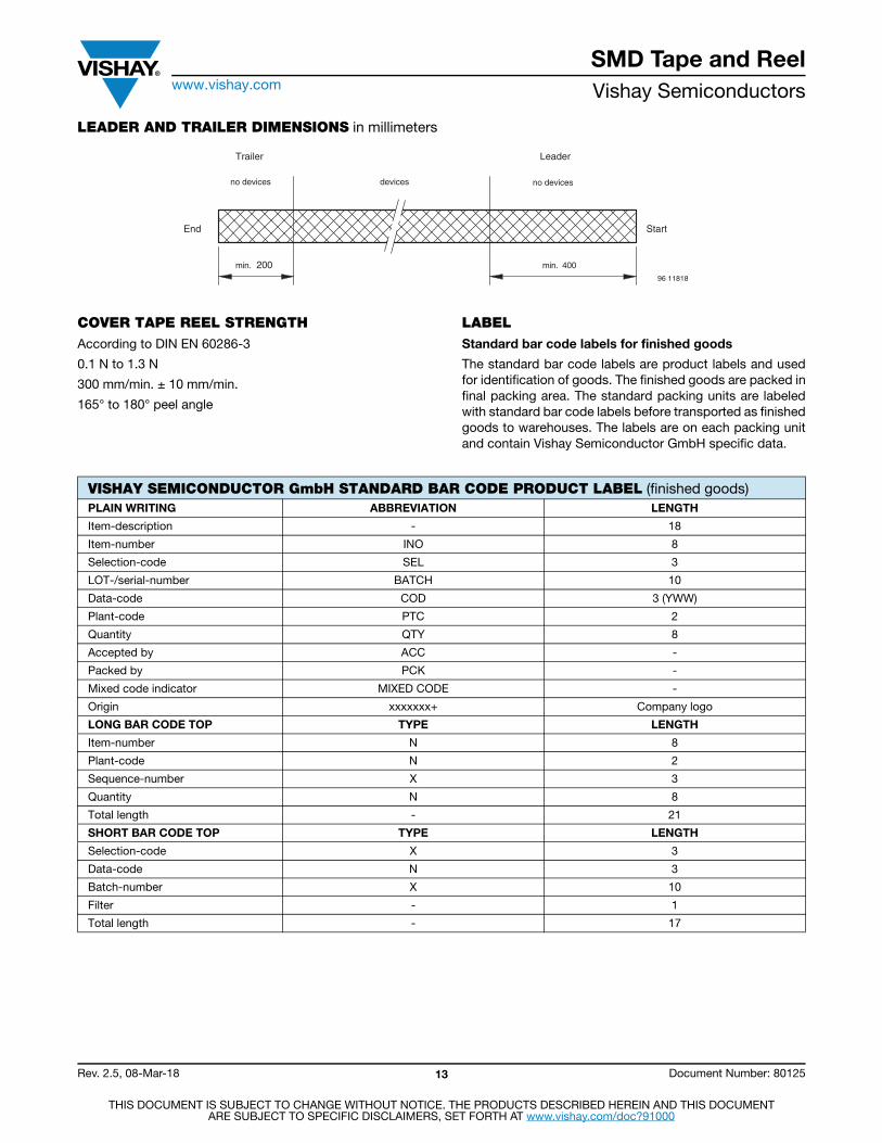
LEADER AND TRAILER DIMENSIONS in millimeters
COVER TAPE REEL STRENGTHAccording to DIN EN 60286-3
0.1 N to 1.3 N
300 mm/min. ± 10 mm/min.
165° to 180° peel angle
LABELStandard bar code labels for finished goods
The standard bar code labels are product labels and used for identification of goods. The finished goods are packed in final packing area. The standard packing units are labeled with standard bar code labels before transported as finished goods to warehouses. The labels are on each packing unit and contain Vishay Semiconductor GmbH specific data.
Trailer Leader
no devices
min. 200 min. 400
StartEnd
devices
96 11818
no devices
VISHAY SEMICONDUCTOR GmbH STANDARD BAR CODE PRODUCT LABEL (finished goods)PLAIN WRITING ABBREVIATION LENGTH
Item-description - 18
Item-number INO 8
Selection-code SEL 3
LOT-/serial-number BATCH 10
Data-code COD 3 (YWW)
Plant-code PTC 2
Quantity QTY 8
Accepted by ACC -
Packed by PCK -
Mixed code indicator MIXED CODE -
Origin xxxxxxx+ Company logo
LONG BAR CODE TOP TYPE LENGTH
Item-number N 8
Plant-code N 2
Sequence-number X 3
Quantity N 8
Total length - 21
SHORT BAR CODE TOP TYPE LENGTH
Selection-code X 3
Data-code N 3
Batch-number X 10
Filter - 1
Total length - 17

SMD Tape and Reelwww.vishay.com Vishay Semiconductors
Rev. 2.5, 08-Mar-18 14 Document Number: 80125
THIS DOCUMENT IS SUBJECT TO CHANGE WITHOUT NOTICE. THE PRODUCTS DESCRIBED HEREIN AND THIS DOCUMENTARE SUBJECT TO SPECIFIC DISCLAIMERS, SET FORTH AT www.vishay.com/doc?91000
DRY PACKAGINGThe reel is packed in an anti-humidity bag to protect the devices from absorbing moisture during transportation and storage.
RECOMMENDED METHOD OF STORAGEDry box storage is recommended as soon as the aluminum bag has been opened to prevent moisture absorption. The following conditions should be observed, if dry boxes are not available:
• Storage temperature 10 °C to 30 °C
• Storage humidity ≤ 60 % RH max.
After more than 72 h under these conditions moisture content will be too high for reflow soldering.
In case of moisture absorption, the devices will recover to the former condition by drying under the following condition:
192 h at 40 °C + 5 °C / - 0 °C and < 5 % RH (dry air / nitrogen) or 96 h at 60 °C + 5 °C and < 5 % RH for all device containers or 24 h at 125 °C + 5 °C not suitable for reel or tubes.
An EIA JEDEC® standard JSTD-020 level 4 label is included on all dry bags.
EIA JEDEC standard JSTD-020 level 4 label is includedon all dry bags
ESD PRECAUTIONProper storage and handling procedures should be followed to prevent ESD damage to the devices especially when they are removed from the antistatic shielding bag. Electrostatic sensitive devices warning labels are on the packaging.
VISHAY SEMICONDUCTORS STANDARD BAR CODE LABELSThe Vishay Semiconductors standard bar code labels are printed at final packing areas. The labels are on each packing unit and contain Vishay Semiconductors specific data.
OUTER PACKAGINGThe sealed reel is packed into a pizza box.
Aluminum bag
Label
Reel
15973
CAUTIONThis bag contains
MOISTURE-SENSITIVE DEVICES
1. Shelf life in sealed bag: 12 months at < 40 °C and < 90 % relative humidity (RH)
2. After this bag is opened, devices that will be subjected to soldering reflow or equivalent processing (peak package body temp. 260 °C) must be2a. Mounted within 72 hours at factory condition of < 30 °C/60 % RH or2b. Stored at < 5 % RH
3. Devices require baking befor mounting if: Humidity Indicator Card is > 10 % when read at 23 °C ± 5 °C or 2a. or 2b. are not met.
4. If baking is required, devices may be baked for: 192 hours at 40 °C + 5 °C/- 0 °C and < 5 % RH (dry air/nitrogen) or 96 hours at 60 °C ± 5 °C and < 5 % RH for all device containers or 24 hours at 125 °C ± 5 °C not suitable for reels or tubes
Bag Seal Date:(If blank, see barcode label)
Note: Level and body temperature defined by EIA JEDEC Standard J-STD-020
4LEVEL
22522
16962
CARTON BOX DIMENSIONS in millimeters
THICKNESS WIDTH LENGTH
Pizza box (SMD and heimdall)(taping in reels)
50 340 340
Thickness
Width 22127
Length

Legal Disclaimer Noticewww.vishay.com Vishay
Revision: 08-Feb-17 1 Document Number: 91000
DisclaimerALL PRODUCT, PRODUCT SPECIFICATIONS AND DATA ARE SUBJECT TO CHANGE WITHOUT NOTICE TO IMPROVE RELIABILITY, FUNCTION OR DESIGN OR OTHERWISE.
Vishay Intertechnology, Inc., its affiliates, agents, and employees, and all persons acting on its or their behalf (collectively, “Vishay”), disclaim any and all liability for any errors, inaccuracies or incompleteness contained in any datasheet or in any other disclosure relating to any product.
Vishay makes no warranty, representation or guarantee regarding the suitability of the products for any particular purpose or the continuing production of any product. To the maximum extent permitted by applicable law, Vishay disclaims (i) any and all liability arising out of the application or use of any product, (ii) any and all liability, including without limitation special, consequential or incidental damages, and (iii) any and all implied warranties, including warranties of fitness for particular purpose, non-infringement and merchantability.
Statements regarding the suitability of products for certain types of applications are based on Vishay’s knowledge of typical requirements that are often placed on Vishay products in generic applications. Such statements are not binding statements about the suitability of products for a particular application. It is the customer’s responsibility to validate that a particular product with the properties described in the product specification is suitable for use in a particular application. Parameters provided in datasheets and / or specifications may vary in different applications and performance may vary over time. All operating parameters, including typical parameters, must be validated for each customer application by the customer’s technical experts. Product specifications do not expand or otherwise modify Vishay’s terms and conditions of purchase, including but not limited to the warranty expressed therein.
Except as expressly indicated in writing, Vishay products are not designed for use in medical, life-saving, or life-sustaining applications or for any other application in which the failure of the Vishay product could result in personal injury or death. Customers using or selling Vishay products not expressly indicated for use in such applications do so at their own risk. Please contact authorized Vishay personnel to obtain written terms and conditions regarding products designed for such applications.
No license, express or implied, by estoppel or otherwise, to any intellectual property rights is granted by this document or by any conduct of Vishay. Product names and markings noted herein may be trademarks of their respective owners.
© 2017 VISHAY INTERTECHNOLOGY, INC. ALL RIGHTS RESERVED