Embed Size (px)
Citation preview
TSL2672Digital Proximity Detector
The TSL2672 family of devices provides proximity detection when coupled with an external IR LED. The devices incorporate a constant-current LED sink driver to pulse the external IR LED and achieve very low average power consumption using the low-power wait state with programmable wait time between proximity measurements. In addition, the devices are register-set and pin-compatible with the TSL2671 series and include a number of new and improved features, such as improved signal-to-noise and measurement accuracy. A proximity offset register allows compensation for optical system crosstalk between the IR LED and the sensor. To prevent false measurements, a proximity saturation bit indicates that the internal analog circuitry saturated. Interrupts have been enhanced with the addition of a sleep-after-interrupt feature that also allows for single-cycle operation.
Ordering Information and Content Guide appear at end of datasheet.
Key Benefits & FeaturesThe benefits and features of TSL2672, Digital Proximity Detector are listed below:
Figure 1:Added Value Of Using TSL2672
• Proximity Detection with an Integrated LED Driver in a Single Device
• Register Set- and Pin-Compatible with the TSL2x71 Series
• Proximity Detection• Reduced Proximity Count Variation• Programmable Offset Control Register• Saturation Indicator• Programmable Analog Gain and Integration Time• Current Sink Driver for External IR LED• 16,000:1 Dynamic Range
Benefits Features
• Enables Operation in IR Light Environments • Patented Dual-Diode Architecture
• Eliminates IR LED System Cross Talk • Programmable Proximity Offset Adjustment
• Prevents False Proximity Detection in Bright Light • Proximity Saturation Indicator Bit
• Allows Multiple Power-level Selection without External Passives
• Programmable LED Drive Current
General Description
ams Datasheet Page 1[v1-01] 2019-Nov-20 Document Feedback
TSL2672 − General Description
• Maskable Proximity Interrupt• Programmable Upper and Lower Thresholds with
Persistence Filter
• Power Management• Low Power 2.2 μA Sleep State with User-Selectable
Sleep-After-Interrupt Mode• 90 μA Wait State with Programmable Wait Time from
2.7 ms to > 8 seconds
• I²C Fast Mode Compatible Interface• Data Rates up to 400 kbit/s• Input Voltage Levels Compatible with VDD or 1.8-V
Bus
• Small 2 mm x 2 mm ODFN Package
ApplicationsTSL2672, Digital Proximity Detector is ideal for:
• Mobile Handset Touchscreen Control and Automatic Speakerphone Enable
• Mechanical Switch Replacement
• Printer Paper Alignment
End Products and Market Segments
• Mobile Handsets, Tablets, Laptops, and HDTVs
• White Goods
• Toys
• Digital Signage
• Printers
Page 2 ams Datasheet Document Feedback [v1-01] 2019-Nov-20
TSL2672 − General Description
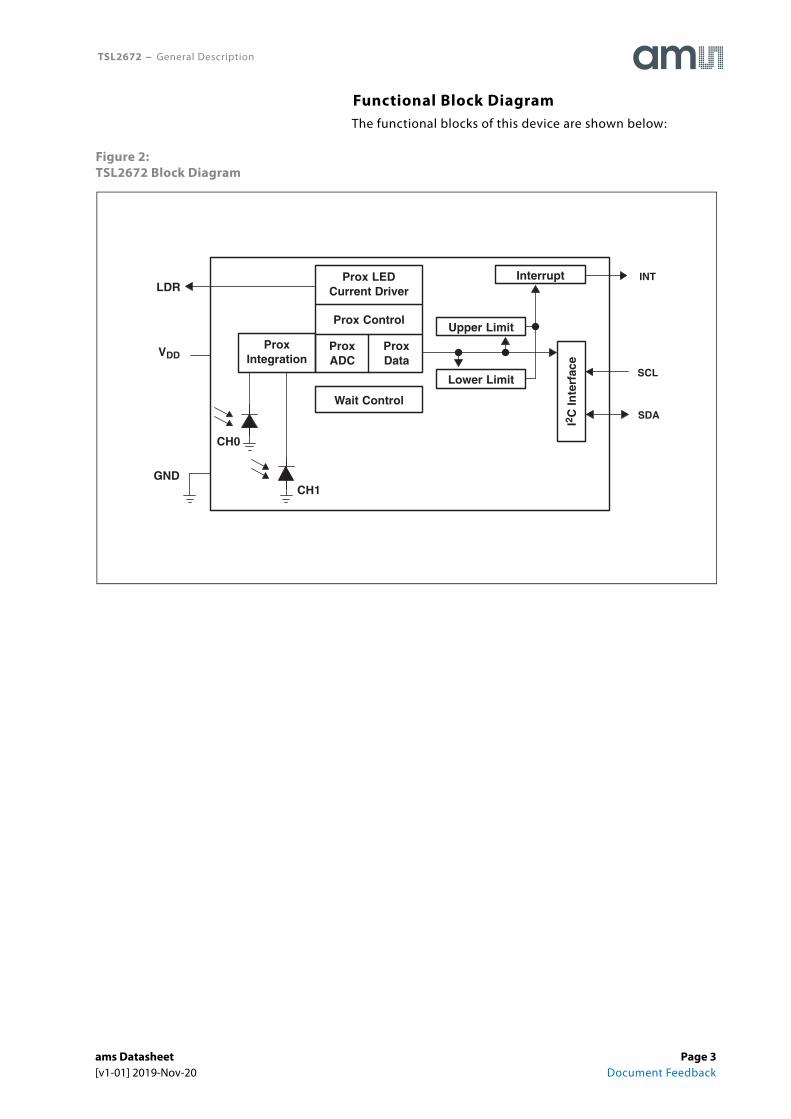
Functional Block DiagramThe functional blocks of this device are shown below:
Figure 2:TSL2672 Block Diagram
CH0
SDA
VDD
INT
SCL
LDR
Wait Control
ProxADC
Prox Control
ProxData
Prox LEDCurrent Driver
ProxIntegration
CH1
Upper Limit
Lower Limit
Interrupt
I2C
Inte
rfac
e
GND
ams Datasheet Page 3[v1-01] 2019-Nov-20 Document Feedback
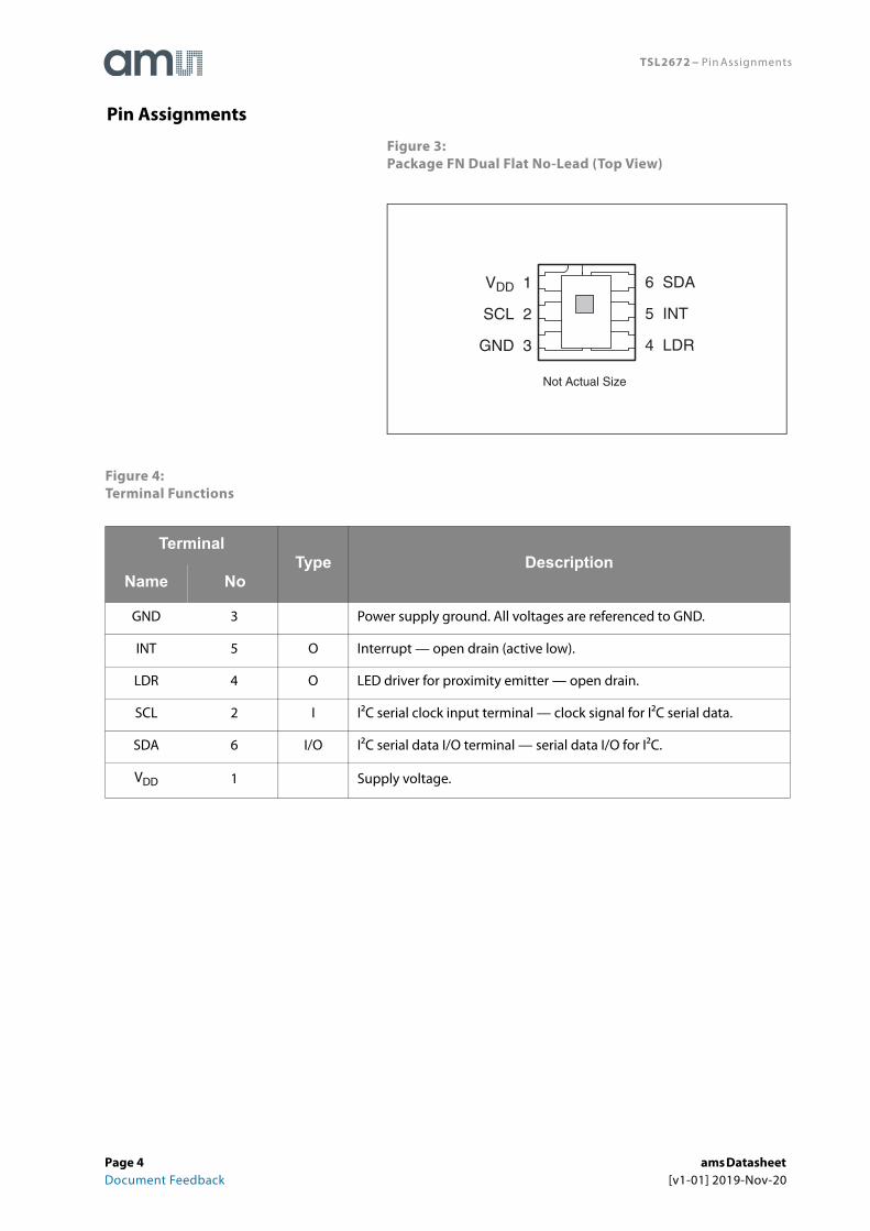
TSL2672 − Pin Assignments
Figure 3:Package FN Dual Flat No-Lead (Top View)
Figure 4:Terminal Functions
TerminalType Description
Name No
GND 3 Power supply ground. All voltages are referenced to GND.
INT 5 O Interrupt — open drain (active low).
LDR 4 O LED driver for proximity emitter — open drain.
SCL 2 I I²C serial clock input terminal — clock signal for I²C serial data.
SDA 6 I/O I²C serial data I/O terminal — serial data I/O for I²C.
VDD 1 Supply voltage.
Pin Assignments
VDD 1
SCL 2
GND 3
6 SDA
5 INT
4 LDR
Not Actual Size
Page 4 ams Datasheet Document Feedback [v1-01] 2019-Nov-20
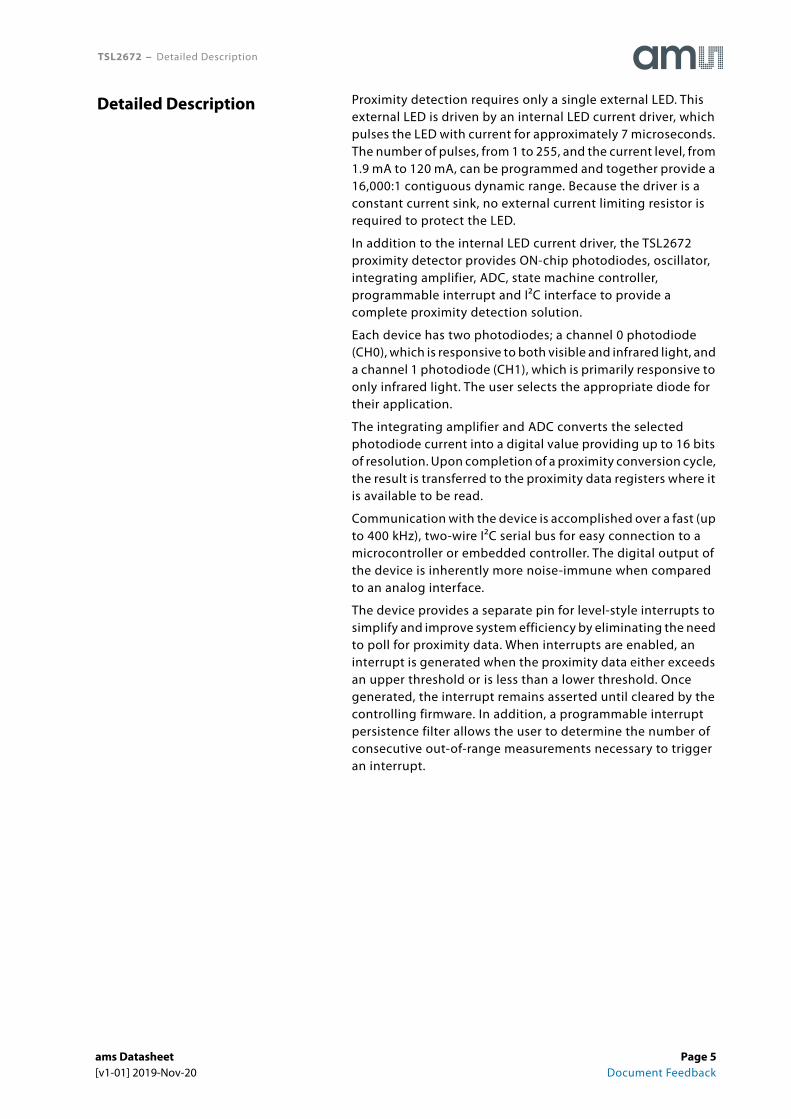
TSL2672 − Detailed Description
Proximity detection requires only a single external LED. This external LED is driven by an internal LED current driver, which pulses the LED with current for approximately 7 microseconds. The number of pulses, from 1 to 255, and the current level, from 1.9 mA to 120 mA, can be programmed and together provide a 16,000:1 contiguous dynamic range. Because the driver is a constant current sink, no external current limiting resistor is required to protect the LED.
In addition to the internal LED current driver, the TSL2672 proximity detector provides ON-chip photodiodes, oscillator, integrating amplifier, ADC, state machine controller, programmable interrupt and I²C interface to provide a complete proximity detection solution.
Each device has two photodiodes; a channel 0 photodiode (CH0), which is responsive to both visible and infrared light, and a channel 1 photodiode (CH1), which is primarily responsive to only infrared light. The user selects the appropriate diode for their application.
The integrating amplifier and ADC converts the selected photodiode current into a digital value providing up to 16 bits of resolution. Upon completion of a proximity conversion cycle, the result is transferred to the proximity data registers where it is available to be read.
Communication with the device is accomplished over a fast (up to 400 kHz), two-wire I²C serial bus for easy connection to a microcontroller or embedded controller. The digital output of the device is inherently more noise-immune when compared to an analog interface.
The device provides a separate pin for level-style interrupts to simplify and improve system efficiency by eliminating the need to poll for proximity data. When interrupts are enabled, an interrupt is generated when the proximity data either exceeds an upper threshold or is less than a lower threshold. Once generated, the interrupt remains asserted until cleared by the controlling firmware. In addition, a programmable interrupt persistence filter allows the user to determine the number of consecutive out-of-range measurements necessary to trigger an interrupt.
Detailed Description
ams Datasheet Page 5[v1-01] 2019-Nov-20 Document Feedback
TSL2672 − Absolute Maximum Ratings
Stresses beyond those listed under Absolute Maximum Ratings may cause permanent damage to the device. These are stress ratings only, and functional operation of the device at these or any other conditions beyond those indicated under Recommended Operating Conditions is not implied. Exposure to absolute-maximum-rated conditions for extended periods may affect device reliability.
Figure 5:Absolute Maximum Ratings Over Operating Free-Air Temperature Range (unless otherwise noted)
Note(s):
1. All voltages are with respect to GND.
Figure 6:Recommended Operating Conditions
Symbol Parameter Min Max Units
VDD(1) Supply voltage 3.8 V
Input terminal voltage -0.5 3.8 V
Output terminal voltage (except LDR) -0.5 3.8 V
Output terminal voltage (LDR) 5 V
Output terminal current (except LDR) -1 20 mA
Tstg Storage temperature range -40 85 °C
ESDHBM ESD tolerance, human body model ±2000 V
Symbol Parameter Conditions Min Nom Max Unit
VDD Supply voltage (TSL26721 & TSL26725) (I²C Vbus = VDD) 2.4 3 3.6 V
VDD Supply voltage (TSL26723 & TSL26727) (I²C Vbus = 1.8 V) 2.7 3 3.6 V
VLDRLED driver
voltage
LDR pulse ON 0 3.6V
LDR pulse OFF 0 4.8
TA
Operating free-air
temperature-30 70 °C
Absolute Maximum Ratings
Page 6 ams Datasheet Document Feedback [v1-01] 2019-Nov-20
TSL2672 − Absolute Maximum Ratings
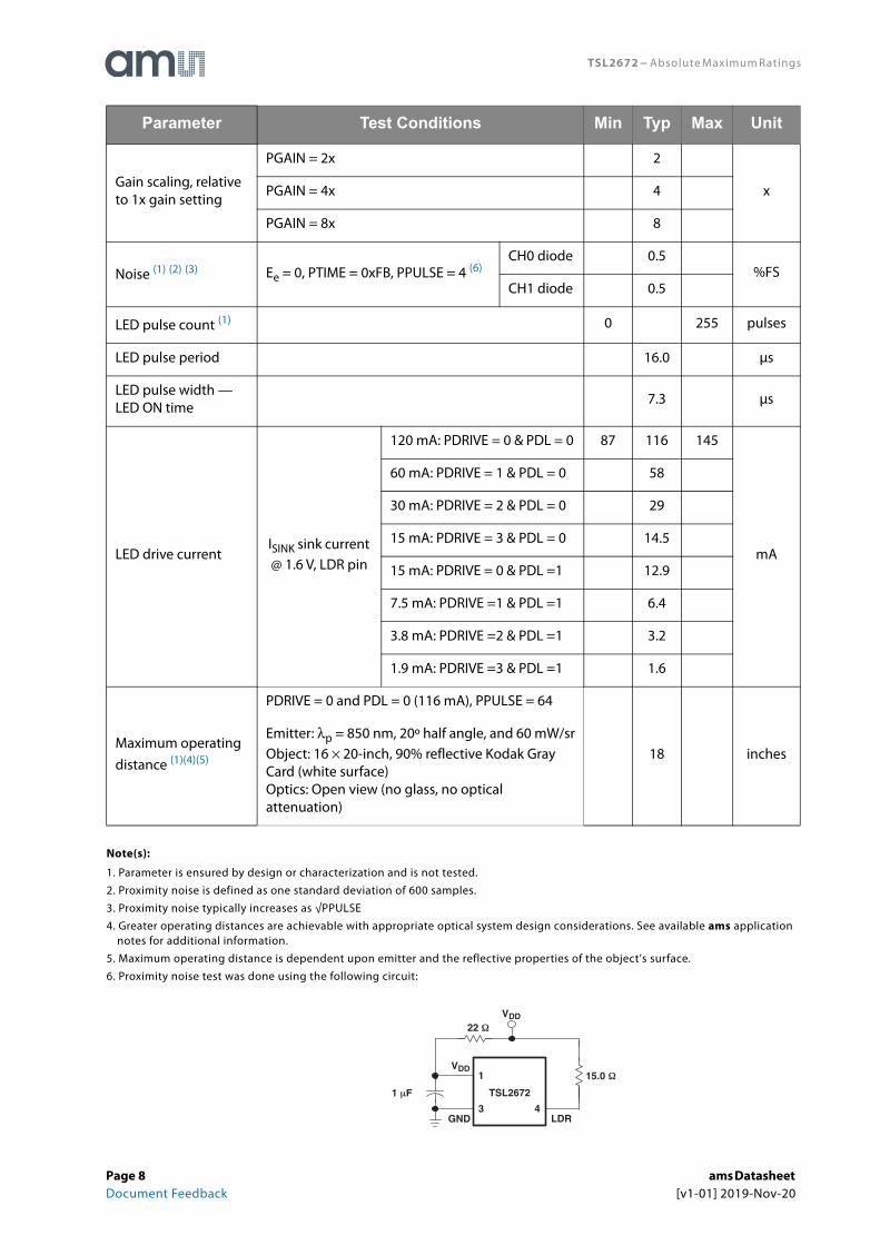
Figure 7:Operating Characteristics; VDD = 3 V, TA = 25°C (unless otherwise noted)
Figure 8:Proximity Characteristics; VDD = 3 V, TA = 25°C, PGAIN = 1´, PEN = 1 (unless otherwise noted)
Symbol Parameter Test Conditions Min Typ Max Unit
IDD Supply current
Active — LDR pulse OFF 200 250
μA Wait state 90
Sleep state - no I²C activity
2.2 4
VOL INT, SDA output low voltage3 mA sink current 0 0.4
V 6 mA sink current 0 0.6
ILEAK Leakage current, SDA, SCL, INT pins
−5 5 μA
ILEAK Leakage current, LDR pin −5 5 μA
VIH SCL, SDA input high voltageTSL26721, TSL26725 0.7 VDD
VTSL26723, TSL26727 1.25
VIL SCL, SDA input low voltageTSL26721, TSL26725 0.3 VDD
V TSL26723, TSL26727 0.54
Parameter Test Conditions Min Typ Max Unit
IDD Supply current
LDR pulse ON 3 mA
ADC conversion time step size
PTIME = 0xFF 2.58 2.73 2.9 ms
ADC number of integration steps (1) 1 256 steps
ADC counts per step (1) PTIME = 0xFF 0 1023 counts
ADC count value λp = 850 nm, Ee = 263.4μW/cm2, PTIME = 0xFB, PPULSE = 4
CH0 diode 1500 2000 2500counts
CH1 diode 900 1200 1500
ADC output responsivity
λp = 850 nm, PTIME = 0xFB, PPULSE = 1
CH0 diode 1.90 counts/μW/cm2CH1 diode 1.14
ams Datasheet Page 7[v1-01] 2019-Nov-20 Document Feedback
TSL2672 − Absolute Maximum Ratings
Note(s):
1. Parameter is ensured by design or characterization and is not tested.
2. Proximity noise is defined as one standard deviation of 600 samples.
3. Proximity noise typically increases as √PPULSE
4. Greater operating distances are achievable with appropriate optical system design considerations. See available ams application notes for additional information.
5. Maximum operating distance is dependent upon emitter and the reflective properties of the object’s surface.
6. Proximity noise test was done using the following circuit:
Gain scaling, relative to 1x gain setting
PGAIN = 2x 2
xPGAIN = 4x 4
PGAIN = 8x 8
Noise (1) (2) (3) Ee = 0, PTIME = 0xFB, PPULSE = 4 (6)CH0 diode 0.5
%FSCH1 diode 0.5
LED pulse count (1) 0 255 pulses
LED pulse period 16.0 μs
LED pulse width — LED ON time
7.3 μs
LED drive currentISINK sink current @ 1.6 V, LDR pin
120 mA: PDRIVE = 0 & PDL = 0 87 116 145
mA
60 mA: PDRIVE = 1 & PDL = 0 58
30 mA: PDRIVE = 2 & PDL = 0 29
15 mA: PDRIVE = 3 & PDL = 0 14.5
15 mA: PDRIVE = 0 & PDL =1 12.9
7.5 mA: PDRIVE =1 & PDL =1 6.4
3.8 mA: PDRIVE =2 & PDL =1 3.2
1.9 mA: PDRIVE =3 & PDL =1 1.6
Maximum operating distance (1)(4)(5)
PDRIVE = 0 and PDL = 0 (116 mA), PPULSE = 64
18 inches Emitter: λp = 850 nm, 20º half angle, and 60 mW/srObject: 16 × 20-inch, 90% reflective Kodak Gray Card (white surface)Optics: Open view (no glass, no optical attenuation)
Parameter Test Conditions Min Typ Max Unit
TSL2672
VDD
1 �F
22 �
15.0 �1
3 4
VDD
GND LDR
Page 8 ams Datasheet Document Feedback [v1-01] 2019-Nov-20
TSL2672 − Absolute Maximum Ratings
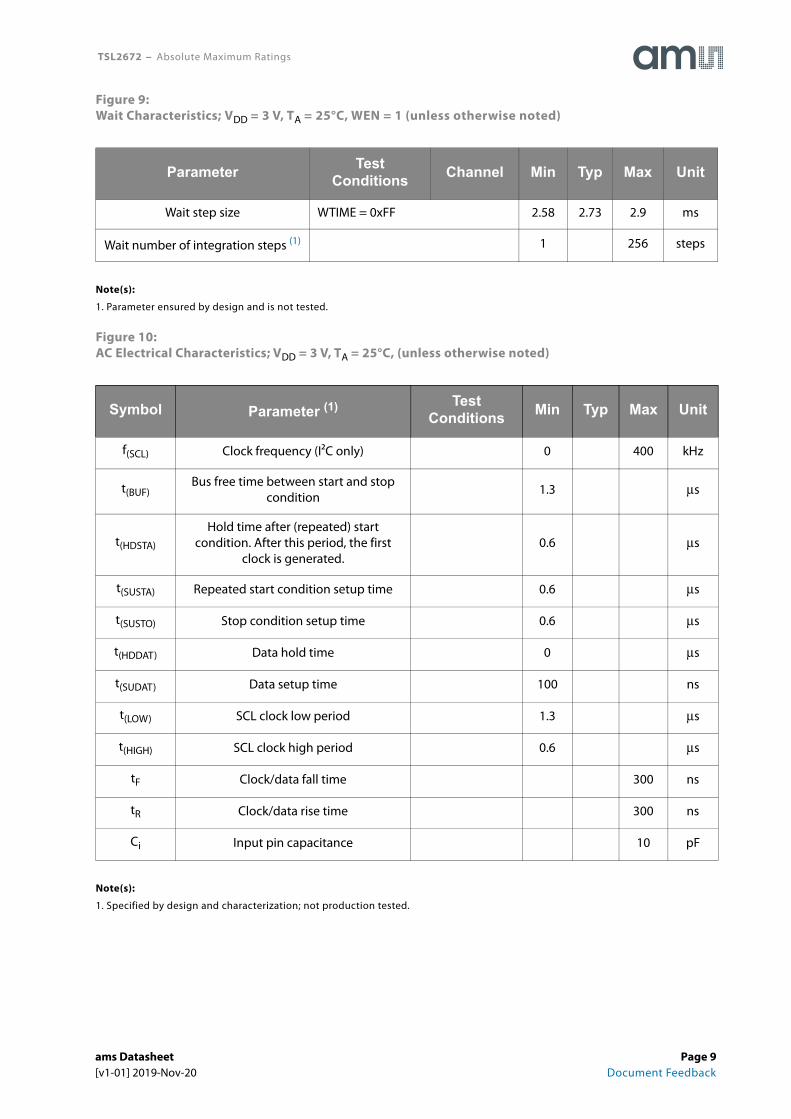
Figure 9:Wait Characteristics; VDD = 3 V, TA = 25°C, WEN = 1 (unless otherwise noted)
Note(s):
1. Parameter ensured by design and is not tested.
Figure 10:AC Electrical Characteristics; VDD = 3 V, TA = 25°C, (unless otherwise noted)
Note(s):
1. Specified by design and characterization; not production tested.
Parameter Test Conditions Channel Min Typ Max Unit
Wait step size WTIME = 0xFF 2.58 2.73 2.9 ms
Wait number of integration steps (1) 1 256 steps
Symbol Parameter (1) Test Conditions Min Typ Max Unit
f(SCL) Clock frequency (I²C only) 0 400 kHz
t(BUF) Bus free time between start and stop
condition 1.3 μs
t(HDSTA) Hold time after (repeated) start
condition. After this period, the first clock is generated.
0.6 μs
t(SUSTA) Repeated start condition setup time 0.6 μs
t(SUSTO) Stop condition setup time 0.6 μs
t(HDDAT) Data hold time 0 μs
t(SUDAT) Data setup time 100 ns
t(LOW) SCL clock low period 1.3 μs
t(HIGH) SCL clock high period 0.6 μs
tF Clock/data fall time 300 ns
tR Clock/data rise time 300 ns
Ci Input pin capacitance 10 pF
ams Datasheet Page 9[v1-01] 2019-Nov-20 Document Feedback
TSL2672 − Absolute Maximum Ratings
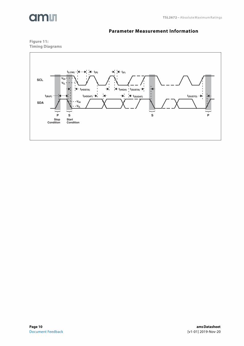
Parameter Measurement Information
Figure 11:Timing Diagrams
StartCondition
StopCondition
P
SDA
t(SUSTO)t(SUDAT)t(HDDAT)t(BUF)
VIH
VIL
SCL
t(SUSTA)t(HIGH)
t(F)t(R)
t(HDSTA)
t(LOW)
VIH
VIL
P SS
Page 10 ams Datasheet Document Feedback [v1-01] 2019-Nov-20
TSL2672 − Typical Characteristics
Figure 12:Spectral Responsivity
Figure 13:Normalized Responsivity vs. Angular Displacement
Typical Characteristics
Ch 1
Ch 0
λ − Wavelength − nm
0400
0.2
0.4
0.6
0.8
1
500 600 700 800 900 1000 1100
No
rmal
ized
Res
po
nsi
vity
300
� − Angular Displacement − °
No
rmal
ized
Res
po
nsi
vity
0
0.2
0.4
0.6
0.8
1.0
−90 −60 −30 0 30 60 90
Op
tica
l Axi
s
�� ��
Both Axes
ams Datasheet Page 11[v1-01] 2019-Nov-20 Document Feedback
TSL2672 − Typical Characteristics
Figure 14:Typical LDR Current vs. Voltage
Figure 15:Typical LDR Current vs. Voltage
30 mA
15 mA
120 mA
LDR Voltage − V
LD
R C
urr
ent
— m
A
0 0.5 1 1.5 2 2.50
20
40
60
80
100
120
140
160
3
60 mA
PDL = 0
15 mA
LDR Voltage − V
LD
R C
urr
ent
— m
A
0 0.5 1 1.5 2 2.50
2
4
6
8
10
12
14
16
3
18
3.8 mA
1.9 mA
7.5 mA
20PDL = 1
Page 12 ams Datasheet Document Feedback [v1-01] 2019-Nov-20
TSL2672 − Typical Characteristics
Figure 16:Response to White LED vs. Temperature
Figure 17:Response to IR (850 nm) LED vs. Temperature
Ch 1
Ch 0
90%
95%
100%
105%
115%
0 10 20 30 40 50 60 70
110%
Temperature − °C
Res
po
nse
— N
orm
aliz
ed t
o 2
5°C
Ch 0
Ch 1
90%
95%
100%
105%
115%
0 10 20 30 40 50 60 70
110%
Temperature − °C
Res
po
nse
— N
orm
aliz
ed t
o 2
5°C
ams Datasheet Page 13[v1-01] 2019-Nov-20 Document Feedback
TSL2672 − Typical Characteristics
Figure 18:Normalized IDD vs.VDD and Temperature
VDD and TEMPERATURE
VDD — V
I DD
— A
ctiv
e C
urr
ent
No
rmal
ized
@ 3
V, 2
5�C
94%
96%
98%
100%
102%
104%
106%
108%
110%
92%2.7 2.8 2.9 3 3.1 3.2 3.3
75�C50�C
0�C
25�C
Page 14 ams Datasheet Document Feedback [v1-01] 2019-Nov-20
TSL2672 − Principles Of Operation
System States An internal state machine provides system control of the proximity detection and power management features of the device. At power up, an internal power-ON-reset initializes the device and puts it in a low-power Sleep state.
When a start condition is detected on the I²C bus, the device transitions to the Idle state where it checks the Enable register (0x00) PON bit. If PON is disabled, the device will return to the Sleep state to save power. Otherwise, the device will remain in the Idle state until the proximity function is enabled. Once enabled, the device will execute the Prox and Wait states in sequence as indicated in Figure 19. Upon completion and return to Idle, the device will automatically begin a new prox-wait cycle as long as PON and PEN remain enabled.
If the Prox function generates an interrupt and the Sleep-After-Interrupt (SAI) feature is enabled, the device will transition to the Sleep state and remain in a low-power mode until an I²C command is received. See the Interrupts section for additional information.
Figure 19:Simplified State Diagram
Principles Of Operation
PEN
Sleep
Idle
WaitProx
I2CStart !PON
INT & SAI
ams Datasheet Page 15[v1-01] 2019-Nov-20 Document Feedback
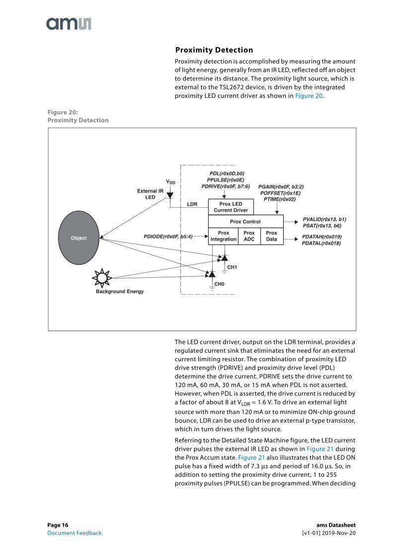
Proximity DetectionProximity detection is accomplished by measuring the amount of light energy, generally from an IR LED, reflected off an object to determine its distance. The proximity light source, which is external to the TSL2672 device, is driven by the integrated proximity LED current driver as shown in Figure 20.
Figure 20:Proximity Detection
The LED current driver, output on the LDR terminal, provides a regulated current sink that eliminates the need for an external current limiting resistor. The combination of proximity LED drive strength (PDRIVE) and proximity drive level (PDL) determine the drive current. PDRIVE sets the drive current to 120 mA, 60 mA, 30 mA, or 15 mA when PDL is not asserted. However, when PDL is asserted, the drive current is reduced by a factor of about 8 at VLDR = 1.6 V. To drive an external light source with more than 120 mA or to minimize ON-chip ground bounce, LDR can be used to drive an external p-type transistor, which in turn drives the light source.
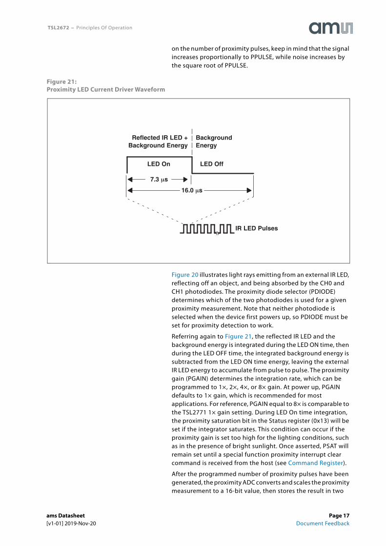
Referring to the Detailed State Machine figure, the LED current driver pulses the external IR LED as shown in Figure 21 during the Prox Accum state. Figure 21 also illustrates that the LED ON pulse has a fixed width of 7.3 μs and period of 16.0 μs. So, in addition to setting the proximity drive current, 1 to 255 proximity pulses (PPULSE) can be programmed. When deciding
CH1
ProxIntegration
Prox Control
ProxADC
Prox LEDCurrent Driver
CH0
PDATAH(r0x019)
PDRIVE(r0x0F, b7:6)
ProxData
External IRLED PTIME(r0x02)
PVALID(r0x13, b1)
VDD
PDL(r0x0D,b0)PPULSE(r0x0E)
PGAIN(r0x0F, b3:2)POFFSET(r0x1E)
PSAT(r0x13, b6)
PDIODE(r0x0F, b5:4)
Background Energy
PDATAL(r0x018)
LDR
Object
Page 16 ams DatasheetDocument Feedback [v1-01] 2019-Nov-20
TSL2672 − Principles Of Operation
on the number of proximity pulses, keep in mind that the signal increases proportionally to PPULSE, while noise increases by the square root of PPULSE.
Figure 21:Proximity LED Current Driver Waveform
Figure 20 illustrates light rays emitting from an external IR LED, reflecting off an object, and being absorbed by the CH0 and CH1 photodiodes. The proximity diode selector (PDIODE) determines which of the two photodiodes is used for a given proximity measurement. Note that neither photodiode is selected when the device first powers up, so PDIODE must be set for proximity detection to work.
Referring again to Figure 21, the reflected IR LED and the background energy is integrated during the LED ON time, then during the LED OFF time, the integrated background energy is subtracted from the LED ON time energy, leaving the external IR LED energy to accumulate from pulse to pulse. The proximity gain (PGAIN) determines the integration rate, which can be programmed to 1×, 2×, 4×, or 8× gain. At power up, PGAIN defaults to 1× gain, which is recommended for most applications. For reference, PGAIN equal to 8× is comparable to the TSL2771 1× gain setting. During LED On time integration, the proximity saturation bit in the Status register (0x13) will be set if the integrator saturates. This condition can occur if the proximity gain is set too high for the lighting conditions, such as in the presence of bright sunlight. Once asserted, PSAT will remain set until a special function proximity interrupt clear command is received from the host (see Command Register).
After the programmed number of proximity pulses have been generated, the proximity ADC converts and scales the proximity measurement to a 16-bit value, then stores the result in two
LED On LED Off
IR LED Pulses
BackgroundEnergy
Reflected IR LED +Background Energy
16.0 �s
7.3 �s
ams Datasheet Page 17[v1-01] 2019-Nov-20 Document Feedback
TSL2672 − Principles Of Operation
8-bit proximity data (PDATAx) registers. ADC scaling is controlled by the proximity ADC conversion time (PTIME) which is programmable from 1 to 256 2.73-ms time units. However, depending on the application, scaling the proximity data will equally scale any accumulated noise. Therefore, in general, it is recommended to leave PTIME at the default value of one 2.73-ms ADC conversion time (0xFF).
In many practical proximity applications, a number of optical system and environmental conditions can produce an offset in the proximity measurement result. To counter these effects, a proximity offset (POFFSET) is provided which allows the proximity data to be shifted positive or negative. Additional information on the use of the proximity offset feature is provided in available ams application notes.
Once the first proximity cycle has completed, the proximity valid (PVALID) bit in the Status register will be set and remain set until the proximity detection function is disabled (PEN).
For additional information on using the proximity detection function behind glass and for optical system design guidance, please see available ams application notes.
Page 18 ams Datasheet Document Feedback [v1-01] 2019-Nov-20
TSL2672 − Principles Of Operation
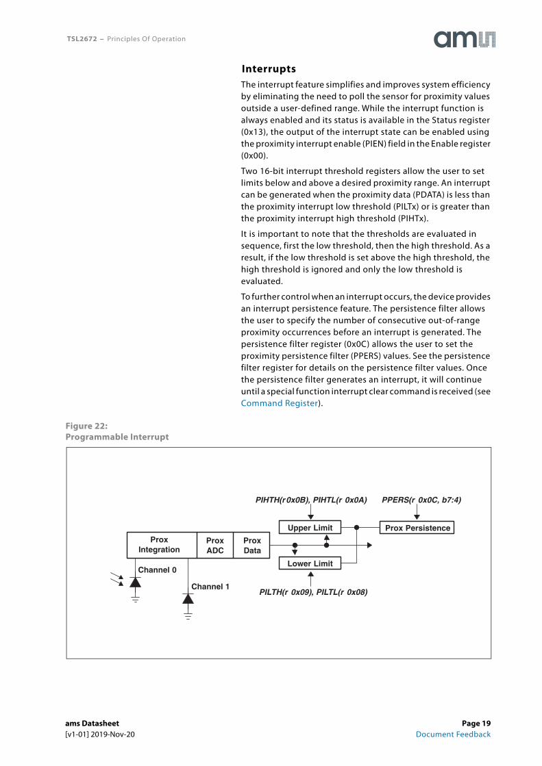
InterruptsThe interrupt feature simplifies and improves system efficiency by eliminating the need to poll the sensor for proximity values outside a user-defined range. While the interrupt function is always enabled and its status is available in the Status register (0x13), the output of the interrupt state can be enabled using the proximity interrupt enable (PIEN) field in the Enable register (0x00).
Two 16-bit interrupt threshold registers allow the user to set limits below and above a desired proximity range. An interrupt can be generated when the proximity data (PDATA) is less than the proximity interrupt low threshold (PILTx) or is greater than the proximity interrupt high threshold (PIHTx).
It is important to note that the thresholds are evaluated in sequence, first the low threshold, then the high threshold. As a result, if the low threshold is set above the high threshold, the high threshold is ignored and only the low threshold is evaluated.
To further control when an interrupt occurs, the device provides an interrupt persistence feature. The persistence filter allows the user to specify the number of consecutive out-of-range proximity occurrences before an interrupt is generated. The persistence filter register (0x0C) allows the user to set the proximity persistence filter (PPERS) values. See the persistence filter register for details on the persistence filter values. Once the persistence filter generates an interrupt, it will continue until a special function interrupt clear command is received (see Command Register).
Figure 22:Programmable Interrupt
ProxADC
ProxData
ProxIntegration
Channel 0
Upper Limit
Lower Limit
Prox Persistence
PILTH(r 0x09), PILTL(r 0x08)
PIHTH(r0x0B), PIHTL(r 0x0A) PPERS(r 0x0C, b7:4)
Channel 1
ams Datasheet Page 19[v1-01] 2019-Nov-20 Document Feedback
TSL2672 − Principles Of Operation
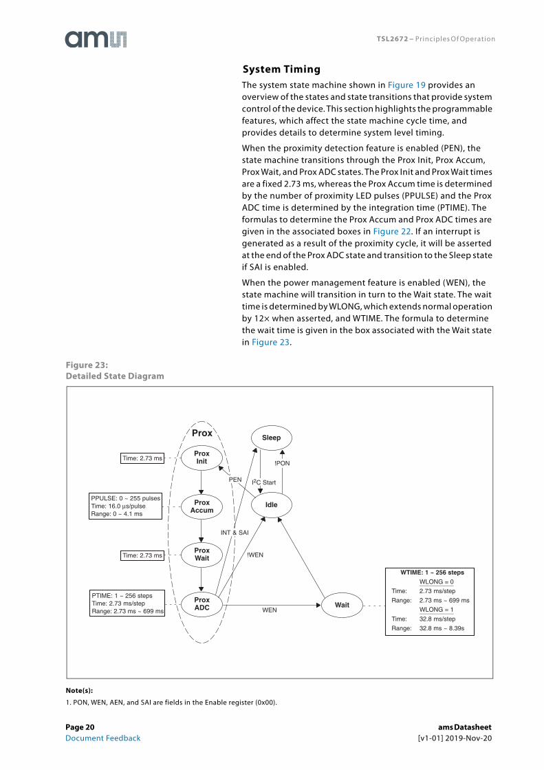
System TimingThe system state machine shown in Figure 19 provides an overview of the states and state transitions that provide system control of the device. This section highlights the programmable features, which affect the state machine cycle time, and provides details to determine system level timing.
When the proximity detection feature is enabled (PEN), the state machine transitions through the Prox Init, Prox Accum, Prox Wait, and Prox ADC states. The Prox Init and Prox Wait times are a fixed 2.73 ms, whereas the Prox Accum time is determined by the number of proximity LED pulses (PPULSE) and the Prox ADC time is determined by the integration time (PTIME). The formulas to determine the Prox Accum and Prox ADC times are given in the associated boxes in Figure 22. If an interrupt is generated as a result of the proximity cycle, it will be asserted at the end of the Prox ADC state and transition to the Sleep state if SAI is enabled.
When the power management feature is enabled (WEN), the state machine will transition in turn to the Wait state. The wait time is determined by WLONG, which extends normal operation by 12× when asserted, and WTIME. The formula to determine the wait time is given in the box associated with the Wait state in Figure 23.
Figure 23:Detailed State Diagram
Note(s):
1. PON, WEN, AEN, and SAI are fields in the Enable register (0x00).
ProxWait
Sleep
Idle
ProxInit
ProxAccum
WaitProxADC
Prox
Time: 2.73 ms
PPULSE: 0 ~ 255 pulsesTime: 16.0 μs/pulseRange: 0 ~ 4.1 ms
Time: 2.73 ms
PTIME: 1 ~ 256 stepsTime: 2.73 ms/stepRange: 2.73 ms ~ 699 ms WEN
!PON
Note: PON, PEN, WEN, and SAI are fields in the Enable register (0x00).
!WEN
PEN
INT & SAI
WTIME: 1 ~ 256 steps
WLONG = 0
Time: 2.73 ms/step
Range: 2.73 ms ~ 699 ms
WLONG = 1
Time: 32.8 ms/step
Range: 32.8 ms ~ 8.39s
I2C Start
Page 20 ams Datasheet Document Feedback [v1-01] 2019-Nov-20
TSL2672 − Principles Of Operation
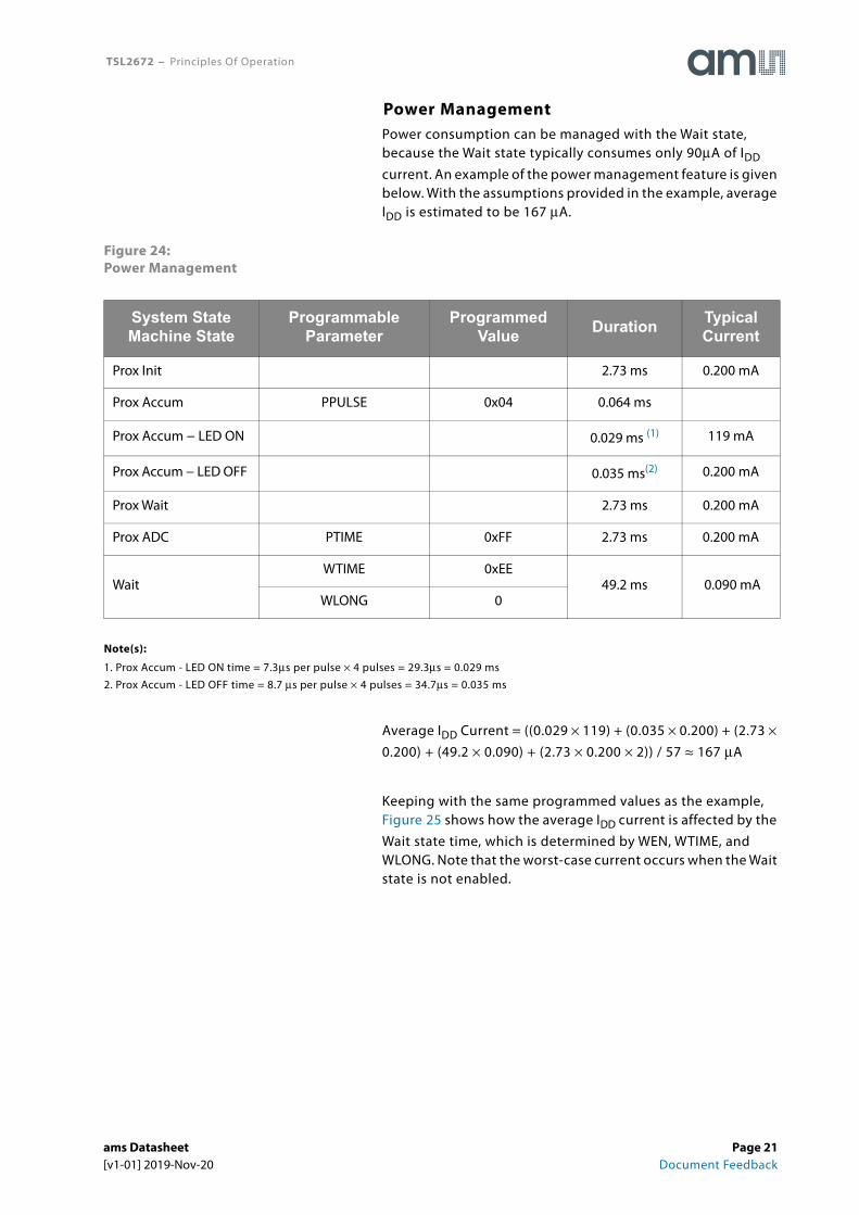
Power ManagementPower consumption can be managed with the Wait state, because the Wait state typically consumes only 90μA of IDD current. An example of the power management feature is given below. With the assumptions provided in the example, average IDD is estimated to be 167 μA.
Figure 24:Power Management
Note(s):
1. Prox Accum - LED ON time = 7.3μs per pulse × 4 pulses = 29.3μs = 0.029 ms
2. Prox Accum - LED OFF time = 8.7 μs per pulse × 4 pulses = 34.7μs = 0.035 ms
Average IDD Current = ((0.029 × 119) + (0.035 × 0.200) + (2.73 × 0.200) + (49.2 × 0.090) + (2.73 × 0.200 × 2)) / 57 ≈ 167 μA
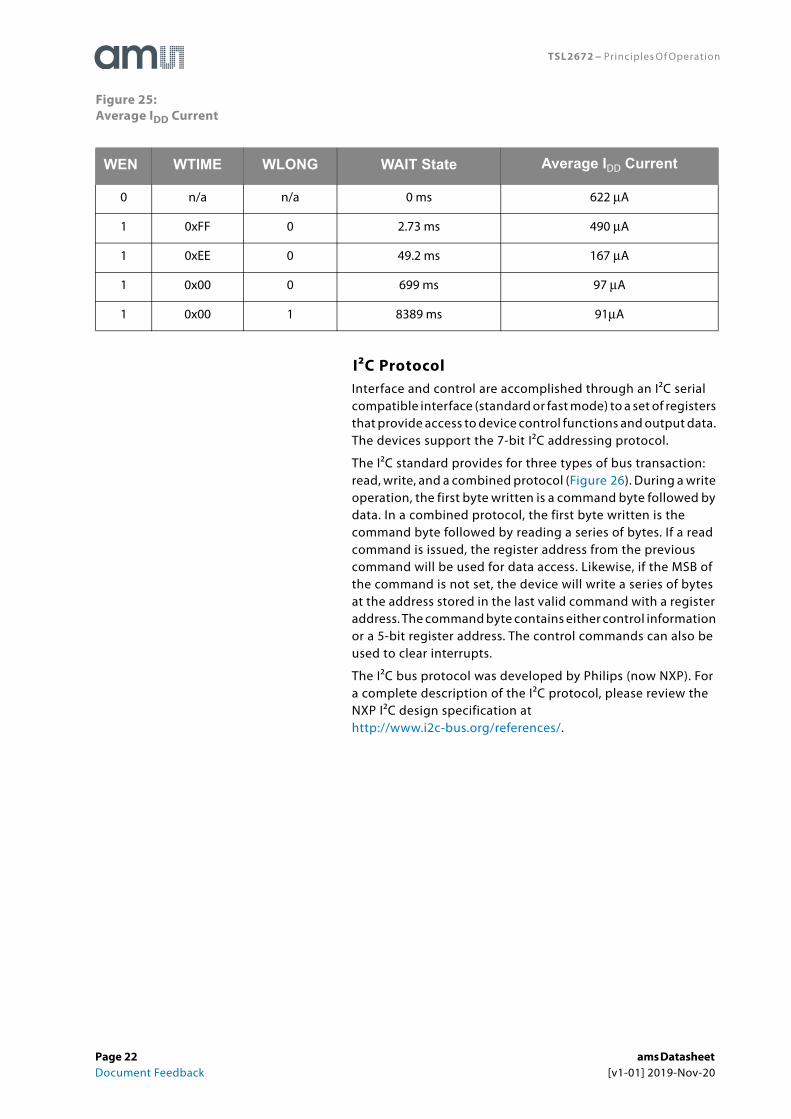
Keeping with the same programmed values as the example, Figure 25 shows how the average IDD current is affected by the Wait state time, which is determined by WEN, WTIME, and WLONG. Note that the worst-case current occurs when the Wait state is not enabled.
System State Machine State
Programmable Parameter
Programmed Value Duration Typical
Current
Prox Init 2.73 ms 0.200 mA
Prox Accum PPULSE 0x04 0.064 ms
Prox Accum − LED ON 0.029 ms (1) 119 mA
Prox Accum − LED OFF 0.035 ms(2) 0.200 mA
Prox Wait 2.73 ms 0.200 mA
Prox ADC PTIME 0xFF 2.73 ms 0.200 mA
WaitWTIME 0xEE
49.2 ms 0.090 mA WLONG 0
ams Datasheet Page 21[v1-01] 2019-Nov-20 Document Feedback
TSL2672 − Principles Of Operation
Figure 25:Average IDD Current
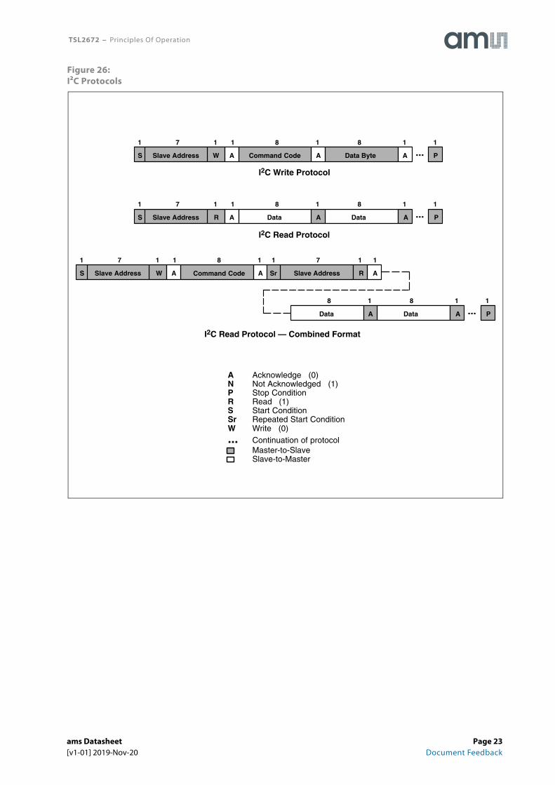
I²C ProtocolInterface and control are accomplished through an I²C serial compatible interface (standard or fast mode) to a set of registers that provide access to device control functions and output data. The devices support the 7-bit I²C addressing protocol.
The I²C standard provides for three types of bus transaction: read, write, and a combined protocol (Figure 26). During a write operation, the first byte written is a command byte followed by data. In a combined protocol, the first byte written is the command byte followed by reading a series of bytes. If a read command is issued, the register address from the previous command will be used for data access. Likewise, if the MSB of the command is not set, the device will write a series of bytes at the address stored in the last valid command with a register address. The command byte contains either control information or a 5-bit register address. The control commands can also be used to clear interrupts.
The I²C bus protocol was developed by Philips (now NXP). For a complete description of the I²C protocol, please review the NXP I²C design specification at http://www.i2c-bus.org/references/.
WEN WTIME WLONG WAIT State Average IDD Current
0 n/a n/a 0 ms 622 μA
1 0xFF 0 2.73 ms 490 μA
1 0xEE 0 49.2 ms 167 μA
1 0x00 0 699 ms 97 μA
1 0x00 1 8389 ms 91μA
Page 22 ams Datasheet Document Feedback [v1-01] 2019-Nov-20
TSL2672 − Principles Of Operation
Figure 26:I²C Protocols
W
7
Data ByteSlave AddressS
1
A AA
81 1 1 8
Command Code
1
P
1
...
I2C Write Protocol
I2C Read Protocol
I2C Read Protocol — Combined Format
R
7
DataSlave AddressS
1
A AA
81 1 1 8
Data
1
P
1
...
W
7
Slave AddressSlave AddressS
1
A RA
81 1 1 7 1 1
Command Code Sr
1
A
Data AA
8 1 8
Data
1
P
1
...
A Acknowledge (0)N Not Acknowledged (1)P Stop ConditionR Read (1)S Start ConditionSr Repeated Start ConditionW Write (0)... Continuation of protocol Master-to-Slave Slave-to-Master
ams Datasheet Page 23[v1-01] 2019-Nov-20 Document Feedback
TSL2672 − Principles Of Operation
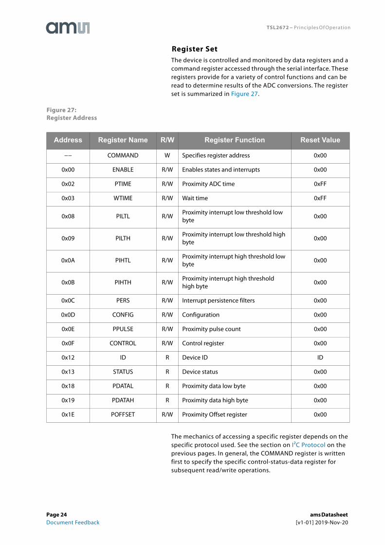
Register SetThe device is controlled and monitored by data registers and a command register accessed through the serial interface. These registers provide for a variety of control functions and can be read to determine results of the ADC conversions. The register set is summarized in Figure 27.
Figure 27:Register Address
The mechanics of accessing a specific register depends on the specific protocol used. See the section on I²C Protocol on the previous pages. In general, the COMMAND register is written first to specify the specific control-status-data register for subsequent read/write operations.
Address Register Name R/W Register Function Reset Value
−− COMMAND W Specifies register address 0x00
0x00 ENABLE R/W Enables states and interrupts 0x00
0x02 PTIME R/W Proximity ADC time 0xFF
0x03 WTIME R/W Wait time 0xFF
0x08 PILTL R/W Proximity interrupt low threshold low byte
0x00
0x09 PILTH R/W Proximity interrupt low threshold high byte
0x00
0x0A PIHTL R/W Proximity interrupt high threshold low byte
0x00
0x0B PIHTH R/W Proximity interrupt high threshold high byte
0x00
0x0C PERS R/W Interrupt persistence filters 0x00
0x0D CONFIG R/W Configuration 0x00
0x0E PPULSE R/W Proximity pulse count 0x00
0x0F CONTROL R/W Control register 0x00
0x12 ID R Device ID ID
0x13 STATUS R Device status 0x00
0x18 PDATAL R Proximity data low byte 0x00
0x19 PDATAH R Proximity data high byte 0x00
0x1E POFFSET R/W Proximity Offset register 0x00
Page 24 ams Datasheet Document Feedback [v1-01] 2019-Nov-20
TSL2672 − Principles Of Operation
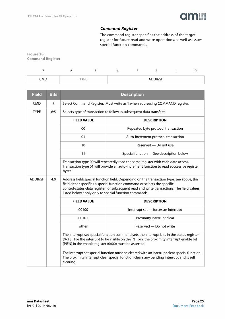
Command RegisterThe command register specifies the address of the target register for future read and write operations, as well as issues special function commands.
Figure 28:Command Register
7 6 5 4 3 2 1 0
CMD TYPE ADDR/SF
Field Bits Description
CMD 7 Select Command Register. Must write as 1 when addressing COMMAND register.
TYPE 6:5 Selects type of transaction to follow in subsequent data transfers:
FIELD VALUE DESCRIPTION
00 Repeated byte protocol transaction
01 Auto-increment protocol transaction
10 Reserved — Do not use
11 Special function — See description below
Transaction type 00 will repeatedly read the same register with each data access. Transaction type 01 will provide an auto-increment function to read successive register bytes.
ADDR/SF 4:0 Address field/special function field. Depending on the transaction type, see above, this field either specifies a special function command or selects the specific control-status-data register for subsequent read and write transactions. The field values listed below apply only to special function commands:
FIELD VALUE DESCRIPTION
00100 Interrupt set — forces an interrupt
00101 Proximity interrupt clear
other Reserved — Do not write
The interrupt set special function command sets the interrupt bits in the status register (0x13). For the interrupt to be visible on the INT pin, the proximity interrupt enable bit (PIEN) in the enable register (0x00) must be asserted.
The interrupt set special function must be cleared with an interrupt clear special function. The proximity interrupt clear special function clears any pending interrupt and is self clearing.
ams Datasheet Page 25[v1-01] 2019-Nov-20 Document Feedback
TSL2672 − Principles Of Operation
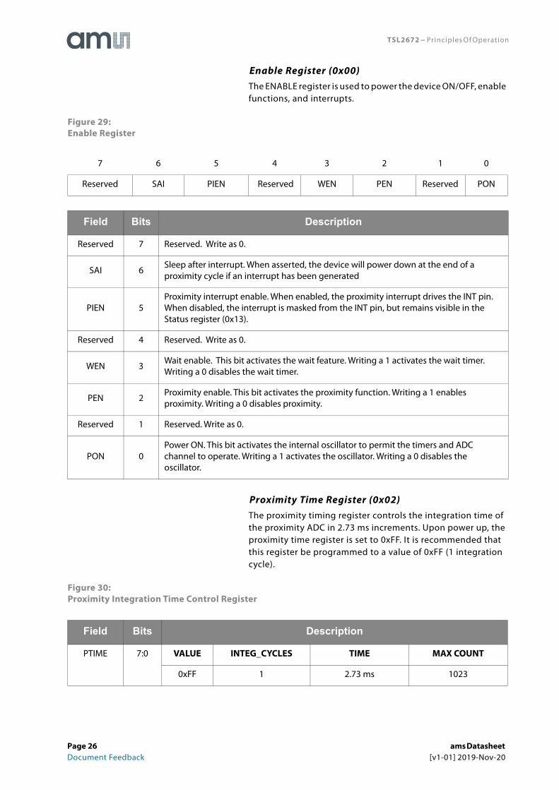
Enable Register (0x00)The ENABLE register is used to power the device ON/OFF, enable functions, and interrupts.
Figure 29:Enable Register
Proximity Time Register (0x02)The proximity timing register controls the integration time of the proximity ADC in 2.73 ms increments. Upon power up, the proximity time register is set to 0xFF. It is recommended that this register be programmed to a value of 0xFF (1 integration cycle).
Figure 30:Proximity Integration Time Control Register
7 6 5 4 3 2 1 0
Reserved SAI PIEN Reserved WEN PEN Reserved PON
Field Bits Description
Reserved 7 Reserved. Write as 0.
SAI 6Sleep after interrupt. When asserted, the device will power down at the end of a proximity cycle if an interrupt has been generated
PIEN 5Proximity interrupt enable. When enabled, the proximity interrupt drives the INT pin. When disabled, the interrupt is masked from the INT pin, but remains visible in the Status register (0x13).
Reserved 4 Reserved. Write as 0.
WEN 3 Wait enable. This bit activates the wait feature. Writing a 1 activates the wait timer. Writing a 0 disables the wait timer.
PEN 2Proximity enable. This bit activates the proximity function. Writing a 1 enables proximity. Writing a 0 disables proximity.
Reserved 1 Reserved. Write as 0.
PON 0 Power ON. This bit activates the internal oscillator to permit the timers and ADC channel to operate. Writing a 1 activates the oscillator. Writing a 0 disables the oscillator.
Field Bits Description
PTIME 7:0 VALUE INTEG_CYCLES TIME MAX COUNT
0xFF 1 2.73 ms 1023
Page 26 ams Datasheet Document Feedback [v1-01] 2019-Nov-20
TSL2672 − Principles Of Operation
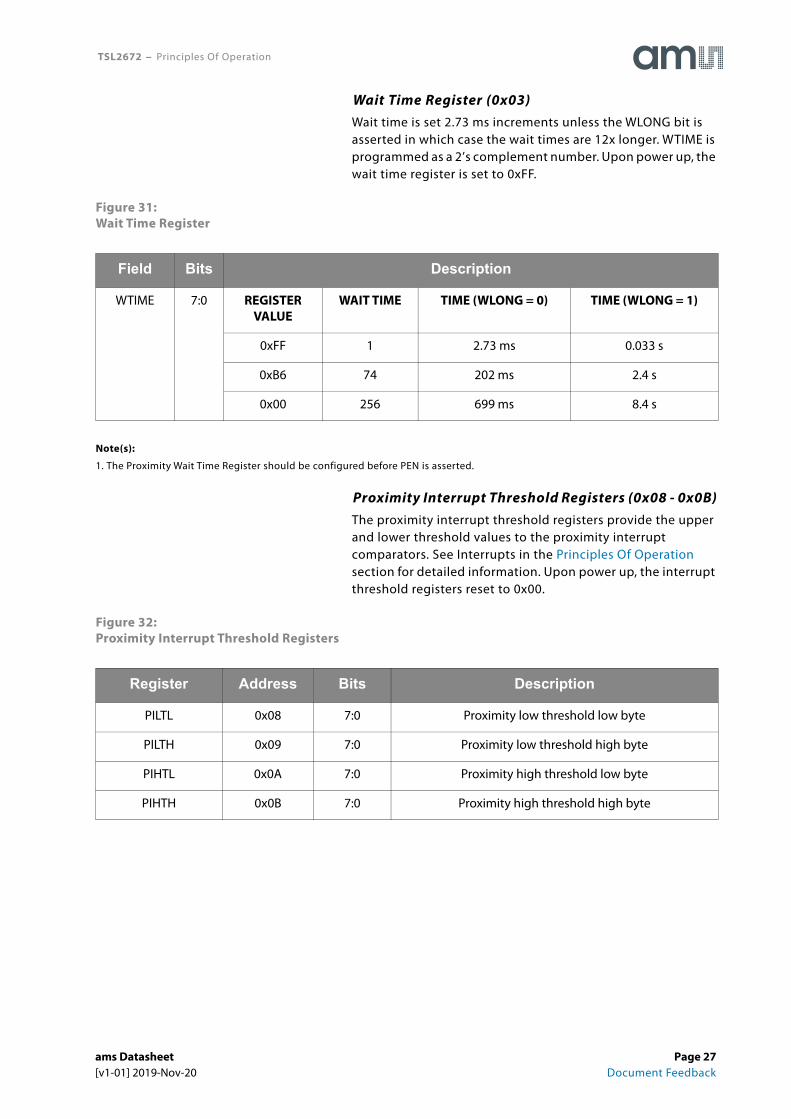
Wait Time Register (0x03)Wait time is set 2.73 ms increments unless the WLONG bit is asserted in which case the wait times are 12x longer. WTIME is programmed as a 2’s complement number. Upon power up, the wait time register is set to 0xFF.
Figure 31:Wait Time Register
Note(s):
1. The Proximity Wait Time Register should be configured before PEN is asserted.
Proximity Interrupt Threshold Registers (0x08 - 0x0B)The proximity interrupt threshold registers provide the upper and lower threshold values to the proximity interrupt comparators. See Interrupts in the Principles Of Operation section for detailed information. Upon power up, the interrupt threshold registers reset to 0x00.
Figure 32:Proximity Interrupt Threshold Registers
Field Bits Description
WTIME 7:0 REGISTER VALUE
WAIT TIME TIME (WLONG = 0) TIME (WLONG = 1)
0xFF 1 2.73 ms 0.033 s
0xB6 74 202 ms 2.4 s
0x00 256 699 ms 8.4 s
Register Address Bits Description
PILTL 0x08 7:0 Proximity low threshold low byte
PILTH 0x09 7:0 Proximity low threshold high byte
PIHTL 0x0A 7:0 Proximity high threshold low byte
PIHTH 0x0B 7:0 Proximity high threshold high byte
ams Datasheet Page 27[v1-01] 2019-Nov-20 Document Feedback
TSL2672 − Principles Of Operation
Interrupt Persistence Filter Register (0x0C)The interrupt persistence filter sets the number of consecutive proximity cycles that are out-of-range before an interrupt is generated. Out-of-range is determined by the proximity interrupt threshold registers (0x08 through 0x0B). See Interrupts in the Principles Of Operation section for further information. Upon power up, the interrupt persistence filter register resets to 0x00, which will generate an interrupt at the end of each proximity cycle.
Figure 33:Interrupt Persistence Filter Register
7 6 5 4 3 2 1 0
PPERS Reserved
Field Bits Description
PPERS 7:4 Proximity persistence. Controls rate of proximity interrupt to the host processor
FIELD VALUE INTERRUPT PERSISTENCE FUNCTION
0000 Every proximity cycle generates an interrupt
0001 1 proximity value out of range
0010 2 consecutive proximity values out of range
... ...
1111 15 consecutive proximity values out of range
Reserved 3:0 Reserved. Write as 0.
Page 28 ams Datasheet Document Feedback [v1-01] 2019-Nov-20
TSL2672 − Principles Of Operation
Configuration Register (0x0D)The configuration register sets the proximity LED drive level and wait long time.
Figure 34:Configuration Register
Proximity Pulse Count Register (0x0E)The proximity pulse count register sets the number of proximity pulses that the LDR pin will generate during the Prox Accum state.
Figure 35:Proximity Pulse Count Register
7 6 5 4 3 2 1 0
Reserved WLONG PDL
Field Bits Description
Reserved 7:2 Reserved. Write as 0.
WLONG 1 Wait Long. When asserted, the wait cycles are increased by a factor 12x from that programmed in the WTIME register.
PDL 0 Proximity drive level. When asserted, the proximity LDR drive current is reduced by 9.
7 6 5 4 3 2 1 0
PPULSE
Field Bits Description
PPULSE 7:0 Proximity Pulse Count. Specifies the number of proximity pulses to be generated.
ams Datasheet Page 29[v1-01] 2019-Nov-20 Document Feedback
TSL2672 − Principles Of Operation
Control Register (0x0F)The Control register provides eight bits of miscellaneous control to the analog block. These bits typically control functions such as gain settings and/or diode selection.
Figure 36:Control Register
Note(s):
1. LED STRENGTH currents are nominal values. Specifications can be found in the Proximity Characteristics table.
7 6 5 4 3 2 1 0
PDRIVE PDIODE PGAIN Reserved
Field Bits Description
PDRIVE(1) 7:6 Proximity LED Drive Strength.
FIELD VALUE LED STRENGTH — PDL = 0 LED STRENGTH — PDL = 1
00 120 mA 15 mA
01 60 mA 7.5 mA
10 30 mA 3.8 mA
11 15 mA 1.9 mA
PDIODE 5:4 Proximity Diode Selector.
FIELD VALUE DIODE SELECTION
00 Proximity uses neither diode
01 Proximity uses the CH0 diode
10 Proximity uses the CH1 diode
11 Reserved — Do not write
PGAIN 3:2 Proximity Gain.
FIELD VALUE PROXIMITY GAIN VALUE
00 1× gain
01 2× gain
10 4× gain
11 8× gain
Reserved 1:0 Reserved. Write as 0.
Page 30 ams Datasheet Document Feedback [v1-01] 2019-Nov-20
TSL2672 − Principles Of Operation
ID Register (0x12)The ID Register provides the value for the part number. The ID register is a read-only register.
Figure 37:ID Register
Status Register (0x13)The Status Register provides the internal status of the device. This register is read only.
Figure 38:Status Register
7 6 5 4 3 2 1 0
ID
Field Bits Description
ID 7:0 Part number identification0x32 = TSL26721 & TSL26725
0x3B = TSL26723 & TSL26727
7 6 5 4 3 2 1 0
Reserved PSAT PINT Reserved PVALID Reserved
Field Bit Description
Reserved 7 Reserved. Read as 0.
PSAT 6 Proximity Saturation. Indicates that the proximity measurement saturated.
PINT 5 Proximity Interrupt. Indicates that the device is asserting a proximity interrupt.
Reserved 4:2 Reserved. Read as 0.
PVALID 1 Proximity Valid. Indicates that the proximity channel has completed an integration cycle after PEN has been asserted.
Reserved 0 Reserved. Read as 0.
ams Datasheet Page 31[v1-01] 2019-Nov-20 Document Feedback
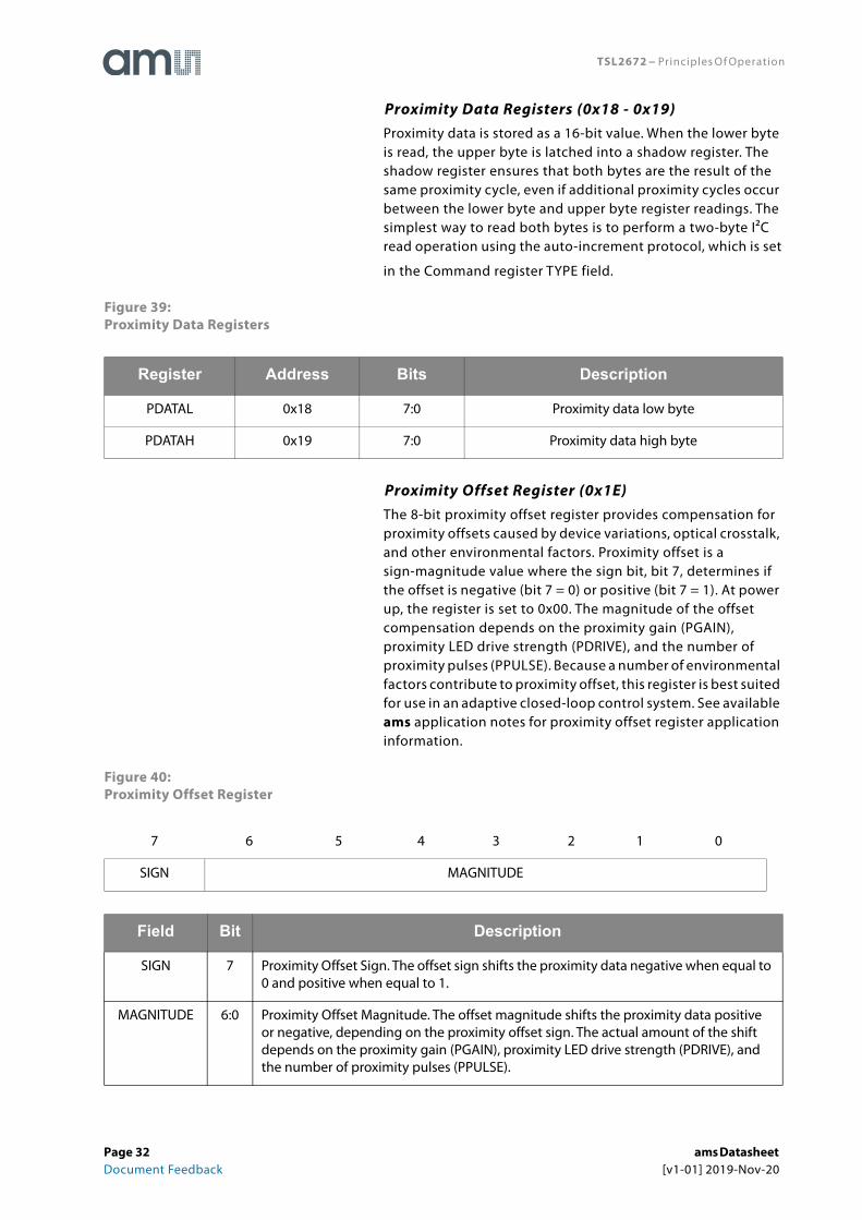
TSL2672 − Principles Of Operation
Proximity Data Registers (0x18 - 0x19)Proximity data is stored as a 16-bit value. When the lower byte is read, the upper byte is latched into a shadow register. The shadow register ensures that both bytes are the result of the same proximity cycle, even if additional proximity cycles occur between the lower byte and upper byte register readings. The simplest way to read both bytes is to perform a two-byte I²C read operation using the auto-increment protocol, which is set
in the Command register TYPE field.
Figure 39:Proximity Data Registers
Proximity Offset Register (0x1E)The 8-bit proximity offset register provides compensation for proximity offsets caused by device variations, optical crosstalk, and other environmental factors. Proximity offset is a sign-magnitude value where the sign bit, bit 7, determines if the offset is negative (bit 7 = 0) or positive (bit 7 = 1). At power up, the register is set to 0x00. The magnitude of the offset compensation depends on the proximity gain (PGAIN), proximity LED drive strength (PDRIVE), and the number of proximity pulses (PPULSE). Because a number of environmental factors contribute to proximity offset, this register is best suited for use in an adaptive closed-loop control system. See available ams application notes for proximity offset register application information.
Figure 40:Proximity Offset Register
Register Address Bits Description
PDATAL 0x18 7:0 Proximity data low byte
PDATAH 0x19 7:0 Proximity data high byte
7 6 5 4 3 2 1 0
SIGN MAGNITUDE
Field Bit Description
SIGN 7 Proximity Offset Sign. The offset sign shifts the proximity data negative when equal to 0 and positive when equal to 1.
MAGNITUDE 6:0 Proximity Offset Magnitude. The offset magnitude shifts the proximity data positive or negative, depending on the proximity offset sign. The actual amount of the shift depends on the proximity gain (PGAIN), proximity LED drive strength (PDRIVE), and the number of proximity pulses (PPULSE).
Page 32 ams Datasheet Document Feedback [v1-01] 2019-Nov-20
TSL2672 − Application Information Hardware
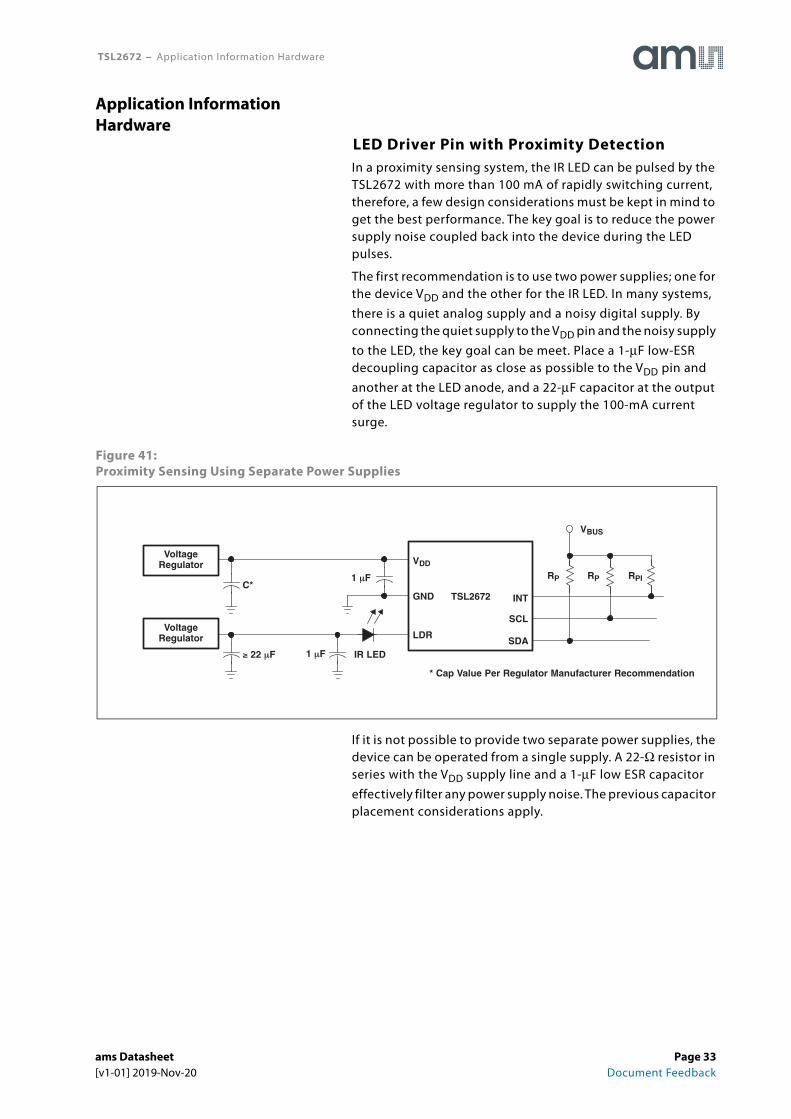
LED Driver Pin with Proximity DetectionIn a proximity sensing system, the IR LED can be pulsed by the TSL2672 with more than 100 mA of rapidly switching current, therefore, a few design considerations must be kept in mind to get the best performance. The key goal is to reduce the power supply noise coupled back into the device during the LED pulses.
The first recommendation is to use two power supplies; one for the device VDD and the other for the IR LED. In many systems, there is a quiet analog supply and a noisy digital supply. By connecting the quiet supply to the VDD pin and the noisy supply to the LED, the key goal can be meet. Place a 1-μF low-ESR decoupling capacitor as close as possible to the VDD pin and another at the LED anode, and a 22-μF capacitor at the output of the LED voltage regulator to supply the 100-mA current surge.
Figure 41:Proximity Sensing Using Separate Power Supplies
If it is not possible to provide two separate power supplies, the device can be operated from a single supply. A 22-Ω resistor in series with the VDD supply line and a 1-μF low ESR capacitor effectively filter any power supply noise. The previous capacitor placement considerations apply.
Application Information Hardware
TSL2672 INT
SDA
SCL
VDD
LDR
1 �F
VoltageRegulator
VoltageRegulator
� 22 �F
* Cap Value Per Regulator Manufacturer Recommendation
IR LED
GND
VBUS
RP RP RPIC*
1 �F
ams Datasheet Page 33[v1-01] 2019-Nov-20 Document Feedback
TSL2672 − Application Information Hardware
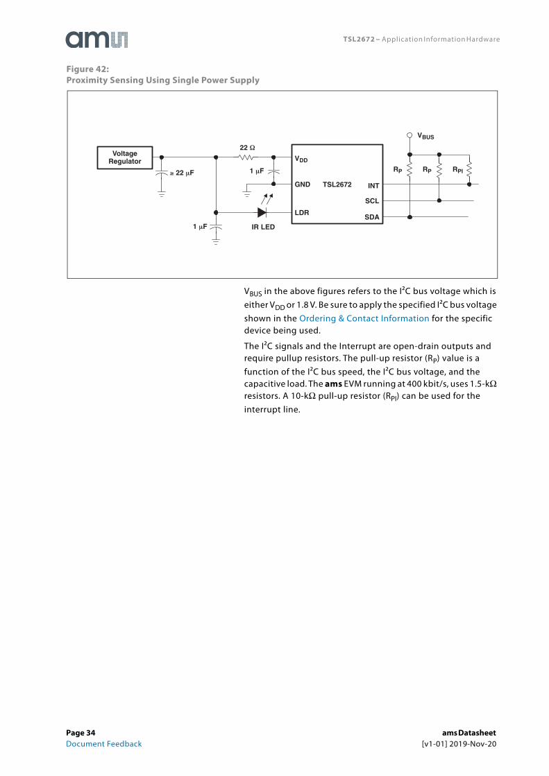
Figure 42:Proximity Sensing Using Single Power Supply
VBUS in the above figures refers to the I²C bus voltage which is either VDD or 1.8 V. Be sure to apply the specified I²C bus voltage shown in the Ordering & Contact Information for the specific device being used.
The I²C signals and the Interrupt are open-drain outputs and require pullup resistors. The pull-up resistor (RP) value is a function of the I²C bus speed, the I²C bus voltage, and the capacitive load. The ams EVM running at 400 kbit/s, uses 1.5-kΩ resistors. A 10-kΩ pull-up resistor (RPI) can be used for the interrupt line.
TSL2672 INT
SDA
SCL
VDD
LDR
1 �F
VoltageRegulator
� 22 �F
IR LED
GND
VBUS
RP RP RPI
1 �F
22 �
Page 34 ams Datasheet Document Feedback [v1-01] 2019-Nov-20
TSL2672 − Application Information Hardware
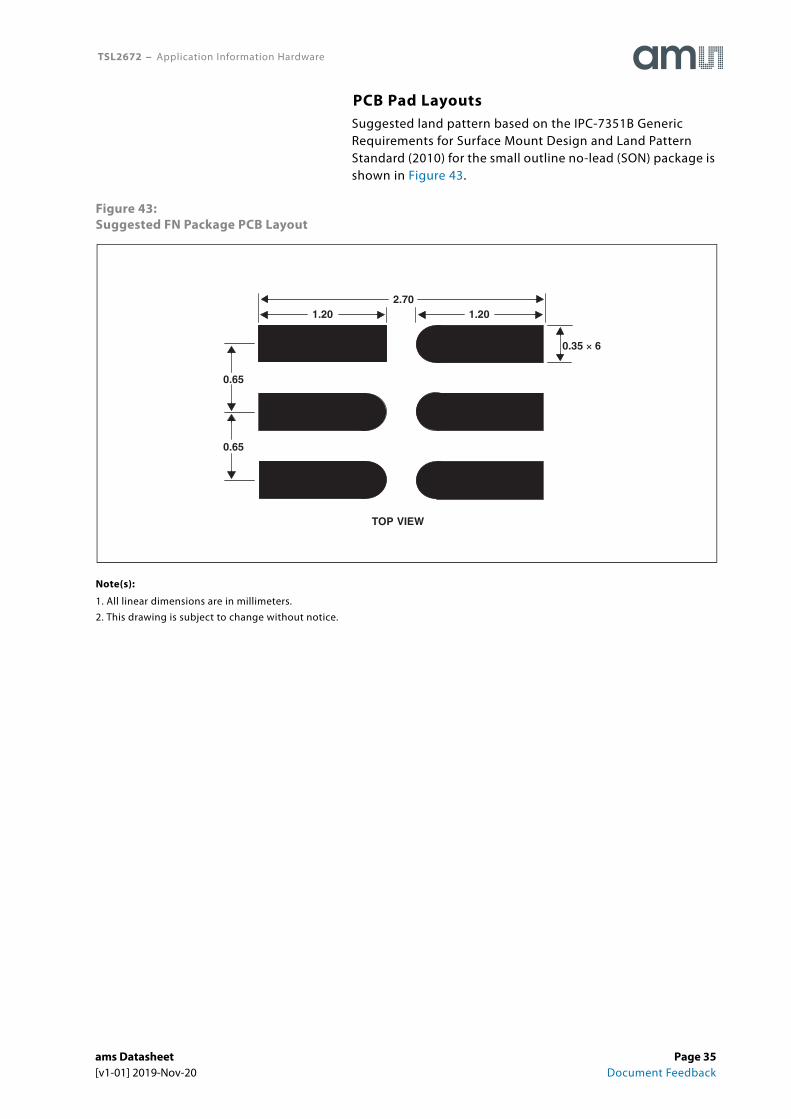
PCB Pad LayoutsSuggested land pattern based on the IPC-7351B Generic Requirements for Surface Mount Design and Land Pattern Standard (2010) for the small outline no-lead (SON) package is shown in Figure 43.
Figure 43:Suggested FN Package PCB Layout
Note(s):
1. All linear dimensions are in millimeters.
2. This drawing is subject to change without notice.
0.35 � 6
2.701.20
0.65
0.65
1.20
TOP VIEW
ams Datasheet Page 35[v1-01] 2019-Nov-20 Document Feedback
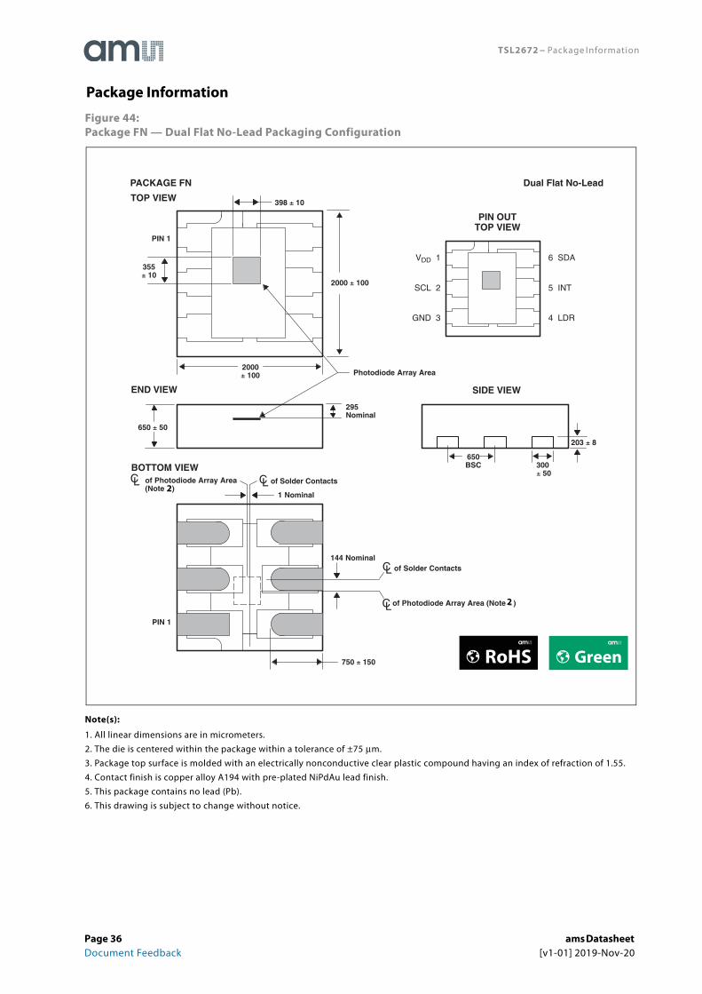
TSL2672 − Package Information
Figure 44:Package FN — Dual Flat No-Lead Packaging Configuration
Note(s):
1. All linear dimensions are in micrometers.
2. The die is centered within the package within a tolerance of ±75 μm.
3. Package top surface is molded with an electrically nonconductive clear plastic compound having an index of refraction of 1.55.
4. Contact finish is copper alloy A194 with pre-plated NiPdAu lead finish.
5. This package contains no lead (Pb).
6. This drawing is subject to change without notice.
Package Information
PACKAGE FN Dual Flat No-Lead
203 � 8
6 SDA
5 INT
4 LDR
VDD 1
SCL 2
GND 3
TOP VIEW
SIDE VIEW
BOTTOM VIEW
Lead Free
Pb
300� 50
650BSC
2000� 100
2000 � 100
PIN 1
PIN 1
END VIEW
650 � 50
PIN OUTTOP VIEW
750 � 150
Photodiode Array Area
295Nominal
355� 10
398 � 10
CL of Solder ContactsCL of Photodiode Array Area(Note B)
1 Nominal
CL of Solder Contacts
of Photodiode Array Area (Note B)CL
144 Nominal
GreenRoHS
2
2
Page 36 ams Datasheet Document Feedback [v1-01] 2019-Nov-20
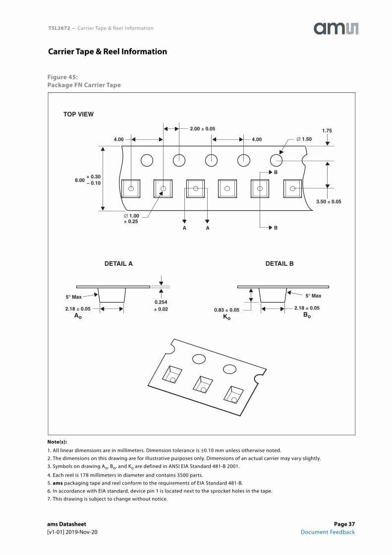
TSL2672 − Carrier Tape & Reel Information
Figure 45:Package FN Carrier Tape
Note(s):
1. All linear dimensions are in millimeters. Dimension tolerance is ±0.10 mm unless otherwise noted.
2. The dimensions on this drawing are for illustrative purposes only. Dimensions of an actual carrier may vary slightly.
3. Symbols on drawing Ao, Bo, and Ko are defined in ANSI EIA Standard 481-B 2001.
4. Each reel is 178 millimeters in diameter and contains 3500 parts.
5. ams packaging tape and reel conform to the requirements of EIA Standard 481-B.
6. In accordance with EIA standard, device pin 1 is located next to the sprocket holes in the tape.
7. This drawing is subject to change without notice.
Carrier Tape & Reel Information
TOP VIEW
DETAIL A
2.18 � 0.05Ao
0.254� 0.02
5� Max
4.00
8.00
3.50 � 0.05
� 1.504.00
2.00 � 0.05
+ 0.30− 0.10
1.75
B
BA A
� 1.00� 0.25
DETAIL B
2.18 � 0.05Bo
5� Max
0.83 � 0.05Ko
ams Datasheet Page 37[v1-01] 2019-Nov-20 Document Feedback
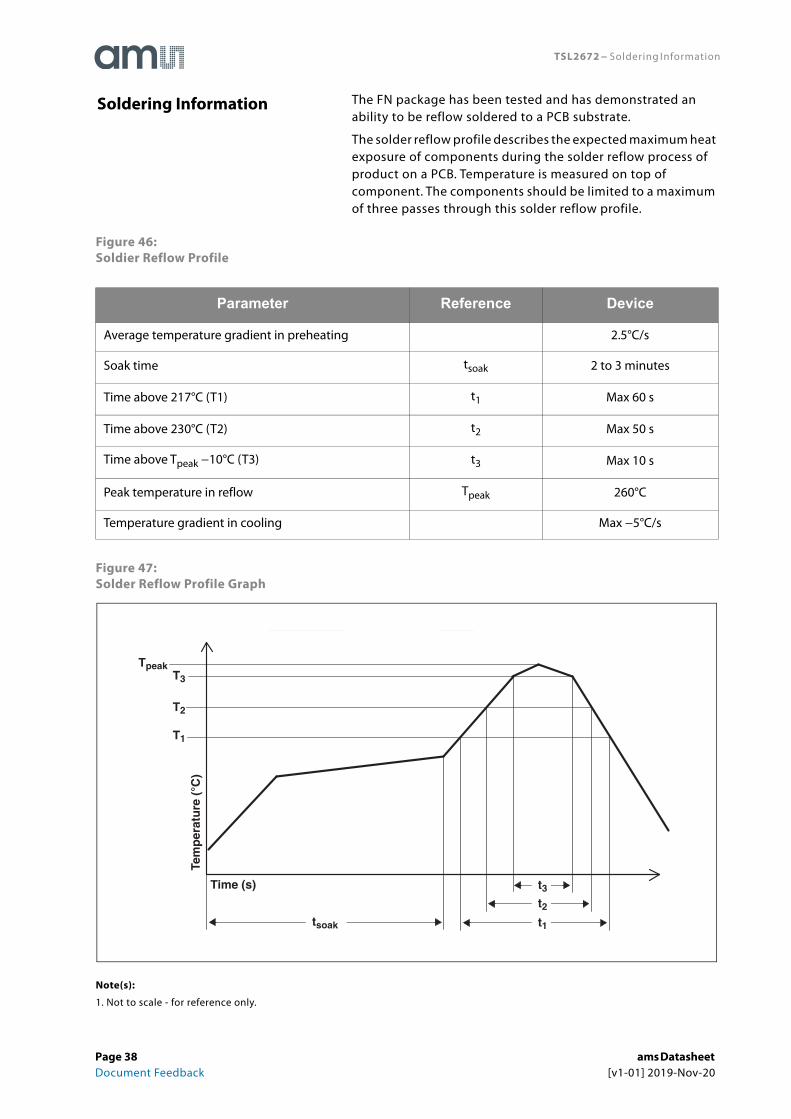
TSL2672 − Soldering Information
The FN package has been tested and has demonstrated an ability to be reflow soldered to a PCB substrate.
The solder reflow profile describes the expected maximum heat exposure of components during the solder reflow process of product on a PCB. Temperature is measured on top of component. The components should be limited to a maximum of three passes through this solder reflow profile.
Figure 46:Soldier Reflow Profile
Figure 47:Solder Reflow Profile Graph
Note(s):
1. Not to scale - for reference only.
Parameter Reference Device
Average temperature gradient in preheating 2.5°C/s
Soak time tsoak 2 to 3 minutes
Time above 217°C (T1) t1 Max 60 s
Time above 230°C (T2) t2 Max 50 s
Time above Tpeak −10°C (T3) t3 Max 10 s
Peak temperature in reflow Tpeak 260°C
Temperature gradient in cooling Max −5°C/s
Soldering Information
t3t2t1tsoak
T3
T2
T1
TpeakNot to scale — for reference o
Time (s)
Tem
per
atu
re (�C
)
Page 38 ams Datasheet Document Feedback [v1-01] 2019-Nov-20
TSL2672 − Storage Information
Moisture SensitivityOptical characteristics of the device can be adversely affected during the soldering process by the release and vaporization of moisture that has been previously absorbed into the package. To ensure the package contains the smallest amount of absorbed moisture possible, each device is dry-baked prior to being packed for shipping. Devices are packed in a sealed aluminized envelope called a moisture barrier bag with silica gel to protect them from ambient moisture during shipping, handling, and storage before use.
Shelf LifeThe calculated shelf life of the device in an unopened moisture barrier bag is 12 months from the date code on the bag when stored under the following conditions:
• Shelf Life: 12 months
• Ambient Temperature: < 40ºC
• Relative Humidity: < 90%
Rebaking of the devices will be required if the devices exceed the 12 month shelf life or the Humidity Indicator Card shows that the devices were exposed to conditions beyond the allowable moisture region.
Floor LifeThe FN package has been assigned a moisture sensitivity level of MSL 3. As a result, the floor life of devices removed from the moisture barrier bag is 168 hours from the time the bag was opened, provided that the devices are stored under the following conditions:
• Floor Life: 168 hours
• Ambient Temperature: < 30ºC
• Relative Humidity: < 60%
If the floor life or the temperature/humidity conditions have been exceeded, the devices must be rebaked prior to solder reflow or dry packing.
Rebaking InstructionsWhen the shelf life or floor life limits have been exceeded, rebake at 50ºC for 12 hours.
Storage Information
ams Datasheet Page 39[v1-01] 2019-Nov-20 Document Feedback
TSL2672 − Ordering & Contact Information
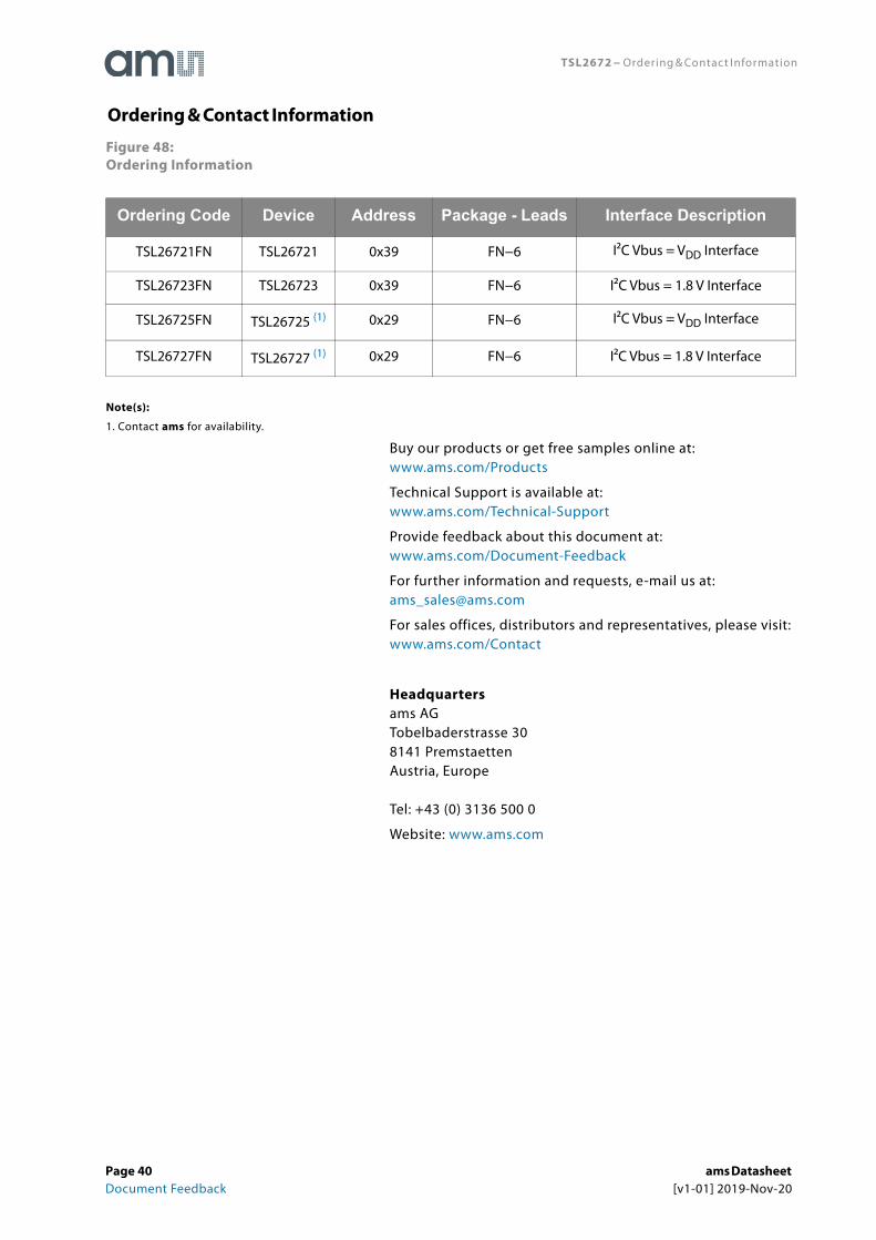
Figure 48:Ordering Information
Note(s):
1. Contact ams for availability.
Buy our products or get free samples online at:www.ams.com/Products
Technical Support is available at: www.ams.com/Technical-Support
Provide feedback about this document at:www.ams.com/Document-Feedback
For further information and requests, e-mail us at:[email protected]
For sales offices, distributors and representatives, please visit: www.ams.com/Contact
Headquartersams AGTobelbaderstrasse 308141 PremstaettenAustria, Europe
Tel: +43 (0) 3136 500 0
Website: www.ams.com
Ordering Code Device Address Package - Leads Interface Description
TSL26721FN TSL26721 0x39 FN−6 I²C Vbus = VDD Interface
TSL26723FN TSL26723 0x39 FN−6 I²C Vbus = 1.8 V Interface
TSL26725FN TSL26725 (1) 0x29 FN−6 I²C Vbus = VDD Interface
TSL26727FN TSL26727 (1) 0x29 FN−6 I²C Vbus = 1.8 V Interface
Ordering & Contact Information
Page 40 ams Datasheet Document Feedback [v1-01] 2019-Nov-20
TSL2672 − RoHS Compliant & ams Green Statement
RoHS: The term RoHS compliant means that ams AG products fully comply with current RoHS directives. Our semiconductor products do not contain any chemicals for all 6 substance categories, including the requirement that lead not exceed 0.1% by weight in homogeneous materials. Where designed to be soldered at high temperatures, RoHS compliant products are suitable for use in specified lead-free processes.
ams Green (RoHS compliant and no Sb/Br): ams Green defines that in addition to RoHS compliance, our products are free of Bromine (Br) and Antimony (Sb) based flame retardants (Br or Sb do not exceed 0.1% by weight in homogeneous material).
Important Information: The information provided in this statement represents ams AG knowledge and belief as of the date that it is provided. ams AG bases its knowledge and belief on information provided by third parties, and makes no representation or warranty as to the accuracy of such information. Efforts are underway to better integrate information from third parties. ams AG has taken and continues to take reasonable steps to provide representative and accurate information but may not have conducted destructive testing or chemical analysis on incoming materials and chemicals. ams AG and ams AG suppliers consider certain information to be proprietary, and thus CAS numbers and other limited information may not be available for release.
RoHS Compliant & ams Green Statement
ams Datasheet Page 41[v1-01] 2019-Nov-20 Document Feedback
TSL2672 − Copyrights & Disclaimer
Copyright ams AG, Tobelbader Strasse 30, 8141 Premstaetten, Austria-Europe. Trademarks Registered. All rights reserved. The material herein may not be reproduced, adapted, merged, translated, stored, or used without the prior written consent of the copyright owner.
Devices sold by ams AG are covered by the warranty and patent indemnification provisions appearing in its General Terms of Trade. ams AG makes no warranty, express, statutory, implied, or by description regarding the information set forth herein. ams AG reserves the right to change specifications and prices at any time and without notice. Therefore, prior to designing this product into a system, it is necessary to check with ams AG for current information. This product is intended for use in commercial applications. Applications requiring extended temperature range, unusual environmental requirements, or high reliability applications, such as military, medical life-support or life-sustaining equipment are specifically not recommended without additional processing by ams AG for each application. This product is provided by ams AG “AS IS” and any express or implied warranties, including, but not limited to the implied warranties of merchantability and fitness for a particular purpose are disclaimed.
ams AG shall not be liable to recipient or any third party for any damages, including but not limited to personal injury, property damage, loss of profits, loss of use, interruption of business or indirect, special, incidental or consequential damages, of any kind, in connection with or arising out of the furnishing, performance or use of the technical data herein. No obligation or liability to recipient or any third party shall arise or flow out of ams AG rendering of technical or other services.
Copyrights & Disclaimer
Page 42 ams Datasheet Document Feedback [v1-01] 2019-Nov-20
TSL2672 − Document Status
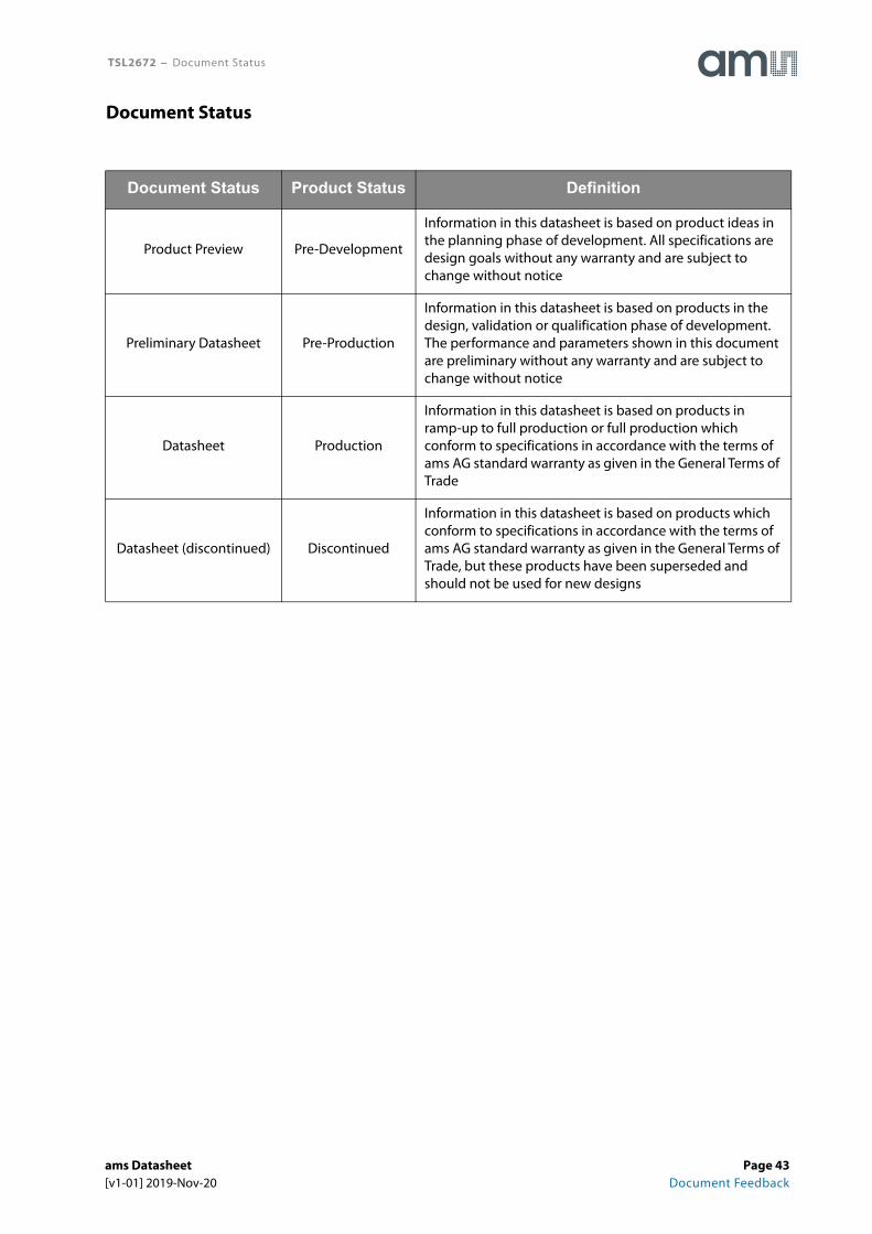
Document Status Product Status Definition
Product Preview Pre-Development
Information in this datasheet is based on product ideas in the planning phase of development. All specifications are design goals without any warranty and are subject to change without notice
Preliminary Datasheet Pre-Production
Information in this datasheet is based on products in the design, validation or qualification phase of development. The performance and parameters shown in this document are preliminary without any warranty and are subject to change without notice
Datasheet Production
Information in this datasheet is based on products in ramp-up to full production or full production which conform to specifications in accordance with the terms of ams AG standard warranty as given in the General Terms of Trade
Datasheet (discontinued) Discontinued
Information in this datasheet is based on products which conform to specifications in accordance with the terms of ams AG standard warranty as given in the General Terms of Trade, but these products have been superseded and should not be used for new designs
Document Status
ams Datasheet Page 43[v1-01] 2019-Nov-20 Document Feedback

TSL2672 − Revision Information
Note(s):
1. Page and figure numbers for the previous version may differ from page and figure numbers in the current revision
2. Correction of typographical errors is not explicitly mentioned.
Changes from 1-00 (2016-Mar-23) to current revision 1-01 (2019-Nov-20) Page
Updated “Key Benefits & Features” (unit mA was replaced with μA) 2
Revision Information
Page 44 ams Datasheet Document Feedback [v1-01] 2019-Nov-20
TSL2672 − Content Guide
1 General Description1 Key Benefits & Features2 Applications2 End Products and Market Segments3 Functional Block Diagram
4 Pin Assignments5 Detailed Description
6 Absolute Maximum Ratings10 Parameter Measurement Information
11 Typical Characteristics
15 Principles Of Operation15 System States16 Proximity Detection19 Interrupts20 System Timing21 Power Management22 I²C Protocol24 Register Set25 Command Register26 Enable Register (0x00)26 Proximity Time Register (0x02)27 Wait Time Register (0x03)27 Proximity Interrupt Threshold Registers (0x08 - 0x0B)28 Interrupt Persistence Filter Register (0x0C)29 Configuration Register (0x0D)29 Proximity Pulse Count Register (0x0E)30 Control Register (0x0F)31 ID Register (0x12)31 Status Register (0x13)32 Proximity Data Registers (0x18 - 0x19)32 Proximity Offset Register (0x1E)
33 Application Information Hardware33 LED Driver Pin with Proximity Detection35 PCB Pad Layouts
36 Package Information37 Carrier Tape & Reel Information38 Soldering Information
39 Storage Information39 Moisture Sensitivity39 Shelf Life39 Floor Life39 Rebaking Instructions
40 Ordering & Contact Information
Content Guide
ams Datasheet Page 45[v1-01] 2019-Nov-20 Document Feedback
TSL2672 − Content Guide
41 RoHS Compliant & ams Green Statement42 Copyrights & Disclaimer43 Document Status44 Revision Information
Page 46 ams Datasheet Document Feedback [v1-01] 2019-Nov-20