Embed Size (px)
Citation preview
AS7265xSmart 18-Channel VIS to NIR Spectral_ID 3-Sensor Chipset with Electronic Shutter
The AS7265x chipset consists of three sensor devices AS72651 with master capability, AS72652 and AS72653. The multispec-tral sensors can be used for spectral identification in a range from visible to NIR. Every of the three sensor devices has 6 in-dependent on-device optical filters whose spectral response is defined in a range from 410nm to 940nm with FWHM of 20nm. The AS72651, combined with the AS72652 (spectral response from 560nm to 940nm) and the AS72653 (spectral response from 410nm to 535nm) form an AS7265x 18-channel multi-spectral sensor chip-set. Using the AS7265x chipset requires the use of firmware. It must be loaded into a serial flash via a UART interface. The list of ams tested serial flash memories can be found in Figure 56. The components AS72651, AS72652 and AS72653 are pre-calibrated with a specific light source. The information about the conditions of the performed calibration (for example light source, gain, integration time) can be found in the table of optical characteristics of the respective compo-nent. Any operation other than these conditions might require a new calibration in the application.
Each AS7265x device has two integrated LED drivers with programmable current and can be timed for electronic shutter applications.
The device family integrates Gaussian filters into standard CMOS silicon via nano-optic deposited interference filter tech-nology in LGA packages that also provide built-in apertures to control the light entering the sensor array.
Ordering Information and Content Guide appear at end of datasheet.
Key Benefits & FeaturesThe benefits and features of AS7265x, Smart 18-Channel VIS to NIR Spectral_ID 3-Sensor Chipset with Electronic Shutter are listed below:
General Description
ams Datasheet Page 1[v1-04] 2018-Jul-09 Document Feedback
AS7265x − General Description
Figure 1:AS7265x Chip-Set Benefits and Features
ApplicationsThe AS7265x applications include:
• Product/Brand authentication
• Anti-counterfeiting
• Portable spectroscopy
• Product safety/adulteration detection
• Horticultural and specialty lighting
• Material analysis
Benefits Features
• Compact 18-channel spectrometry chip-set solution
• 3 chip set including master device delivering 18 visible and NIR channels from 410nm to 940nm each with 20nm FWHM
• UART or I²C slave digital Interface
• Visible filter set realized by silicon interference filters
• No additional signal conditioning required
• 16-bit ADC with digital access
• Programmable LED drivers
• 2.7V to 3.6V with I²C interface
• Small, robust package, with built-in aperture• 20-pin LGA package 4.5mm x 4.7mm x 2.5mm
-40°C to 85°C temperature range
Page 2 ams Datasheet Document Feedback [v1-04] 2018-Jul-09

AS7265x − General Description
Block DiagramThe functional blocks of this device are shown below:
Figure 2:AS7265x Chip-Set Block Diagram
Note(s):
1. Refer to the Application Diagram in Figure 60.
VDD1 VDD2
GND
MISO
SCK
MOSI
CSN
SCL_M
SDA_M
RESN
°C
TX / SDA_S
Current
Control
LED_IND
LED_DRVRX / SCL_S UART or
I2C Slave
I2C Master
SPI
Master
OSC
16MHz
WVU
VDD
VDD
VDD
VDD
Communication
Firmware Interface
LED DriversSpectral_ID
Sensor
I2C_ENB
INT
TSR
VDD1 VDD2
GND
RESN
°C
SDA_S
Current
Control
LED_IND
LED_DRV
SCL_SI2C Slave
OSC
16MHz
LKJ
VDD VDD
Communication LED Drivers
Spectral_ID Sensor
IHG
VDD1 VDD2
GND
RESN
°C
SDA_S
Current
Control
LED_IND
LED_DRV
SCL_SI2C Slave
OSC
16MHz
FED
VDD VDD
Communication LED Drivers
Spectral_ID Sensor
CBA
Micro Controller
Unit (MCU)
AS72651
AS72652 AS72653
Serial Flash MemorySLV2_RESN
SLV1_RESN
ams Datasheet Page 3[v1-04] 2018-Jul-09 Document Feedback
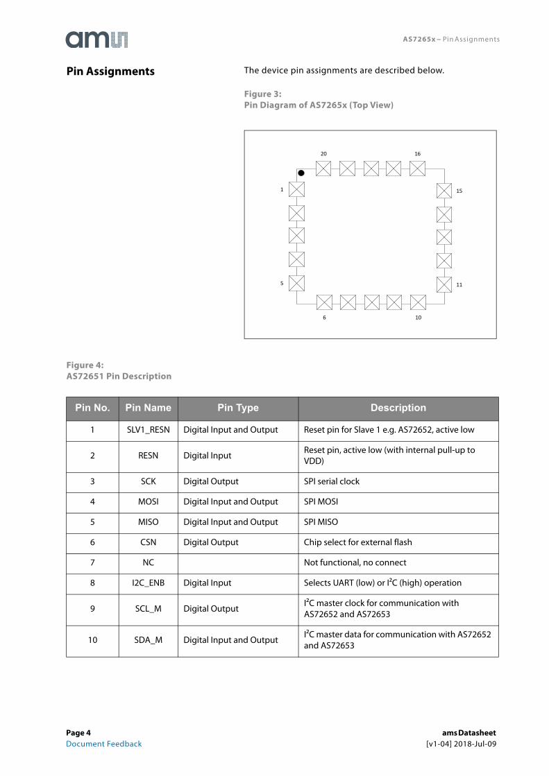
AS7265x − Pin Assignments
The device pin assignments are described below.
Figure 3:Pin Diagram of AS7265x (Top View)
Figure 4:AS72651 Pin Description
Pin No. Pin Name Pin Type Description
1 SLV1_RESN Digital Input and Output Reset pin for Slave 1 e.g. AS72652, active low
2 RESN Digital InputReset pin, active low (with internal pull-up to VDD)
3 SCK Digital Output SPI serial clock
4 MOSI Digital Input and Output SPI MOSI
5 MISO Digital Input and Output SPI MISO
6 CSN Digital Output Chip select for external flash
7 NC Not functional, no connect
8 I2C_ENB Digital Input Selects UART (low) or I²C (high) operation
9 SCL_M Digital OutputI²C master clock for communication with AS72652 and AS72653
10 SDA_M Digital Input and OutputI²C master data for communication with AS72652 and AS72653
Pin Assignments
1
5
6 10
11
15
1620
Page 4 ams Datasheet Document Feedback [v1-04] 2018-Jul-09

AS7265x − Pin Assignments
Note(s):
1. Pin out is valid for firmware versions from 11 and later.
Figure 5:AS72652 and AS72653 Pin Description
11 RX / SCL_S Digital Input and OutputRX (UART) or SCL_S (I²C slave) depending on I2C_ENB setting
12 TX / SDA_S Digital Input and OutputTX (UART) or SDA_S (I²C slave) depending on I2C_ENB setting
13 INT Digital Output INT is active low
14 VDD2 Voltage Supply Voltage supply
15 LED_DRV Analog Output LED driver output for driver LED, current sink
16 GND Supply Ground
17 VDD1 Voltage Supply Voltage supply
18 LED_IND Analog Output LED driver output for indicator LED, current sink
19 NC Not functional, no connect
20 SLV2_RESN Digital Output Reset pin for slave 2 e.g. AS72653, active low
Pin No. Pin Name Pin Type Description
1 NC Not functional, no connect
2 RESN Digital InputReset pin, active low (with internal pull-up to VDD)
3 NC Not functional, no connect
4 NC Not functional, no connect
5 NC Not functional, no connect
6 NC Not functional, no connect
7 NC Not functional, no connect
8 NC Not functional, no connect
9 SCL_S Digital Input and OutputI²C slave clock for communication with master AS72651
10 SDA_S Digital Input and OutputI²C slave data for communication with master AS72651
Pin No. Pin Name Pin Type Description
ams Datasheet Page 5[v1-04] 2018-Jul-09 Document Feedback

AS7265x − Pin Assignments
11 NC Not functional, no connect
12 NC Not functional, no connect
13 INT Digital Output INT is active low
14 VDD2 Voltage Supply Voltage supply
15 LED_DRV Analog Output LED driver output for driver LED, current sink
16 GND Supply Ground
17 VDD1 Voltage Supply Voltage supply
18 LED_IND Analog Output LED driver output for indicator LED, current sink
19 NC Not functional, no connect
20 NC Not functional, no connect
Pin No. Pin Name Pin Type Description
Page 6 ams Datasheet Document Feedback [v1-04] 2018-Jul-09
AS7265x − Absolute Maximum Ratings
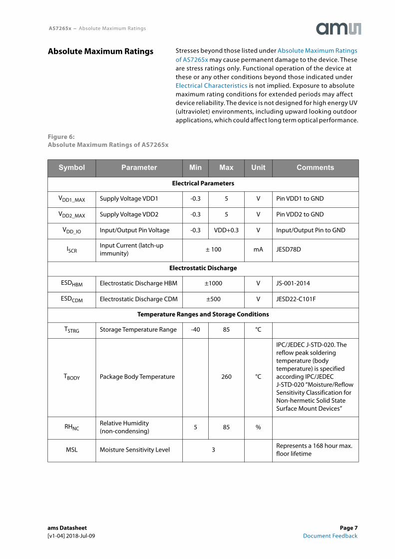
Stresses beyond those listed under Absolute Maximum Ratings of AS7265x may cause permanent damage to the device. These are stress ratings only. Functional operation of the device at these or any other conditions beyond those indicated underElectrical Characteristics is not implied. Exposure to absolute maximum rating conditions for extended periods may affect device reliability. The device is not designed for high energy UV (ultraviolet) environments, including upward looking outdoor applications, which could affect long term optical performance.
Figure 6:Absolute Maximum Ratings of AS7265x
Symbol Parameter Min Max Unit Comments
Electrical Parameters
VDD1_MAX Supply Voltage VDD1 -0.3 5 V Pin VDD1 to GND
VDD2_MAX Supply Voltage VDD2 -0.3 5 V Pin VDD2 to GND
VDD_IO Input/Output Pin Voltage -0.3 VDD+0.3 V Input/Output Pin to GND
ISCRInput Current (latch-up immunity)
± 100 mA JESD78D
Electrostatic Discharge
ESDHBM Electrostatic Discharge HBM ±1000 V JS-001-2014
ESDCDM Electrostatic Discharge CDM ±500 V JESD22-C101F
Temperature Ranges and Storage Conditions
TSTRG Storage Temperature Range -40 85 °C
TBODY Package Body Temperature 260 °C
IPC/JEDEC J-STD-020. The reflow peak soldering temperature (body temperature) is specified according IPC/JEDEC J-STD-020 “Moisture/Reflow Sensitivity Classification for Non-hermetic Solid State Surface Mount Devices”
RHNCRelative Humidity (non-condensing)
5 85 %
MSL Moisture Sensitivity Level 3Represents a 168 hour max. floor lifetime
Absolute Maximum Ratings
ams Datasheet Page 7[v1-04] 2018-Jul-09 Document Feedback
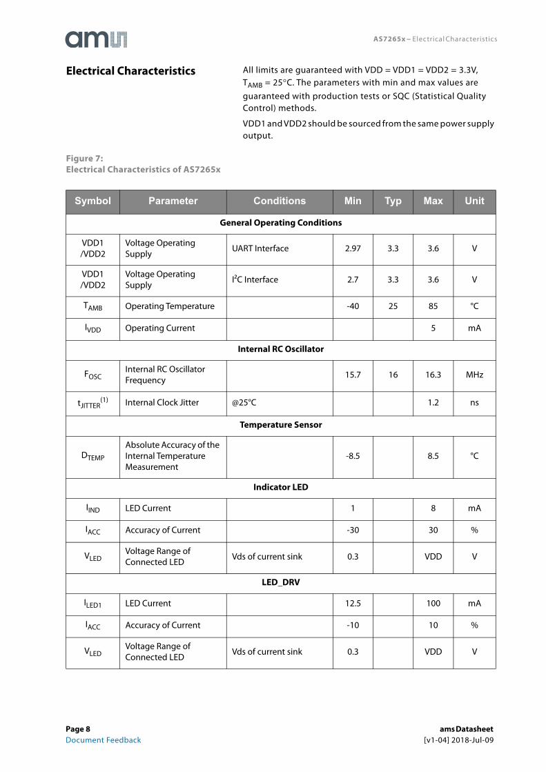
AS7265x − Electrical Characteristics
All limits are guaranteed with VDD = VDD1 = VDD2 = 3.3V, TAMB = 25°C. The parameters with min and max values are guaranteed with production tests or SQC (Statistical Quality Control) methods.
VDD1 and VDD2 should be sourced from the same power supply output.
Figure 7:Electrical Characteristics of AS7265x
Symbol Parameter Conditions Min Typ Max Unit
General Operating Conditions
VDD1 /VDD2
Voltage Operating Supply
UART Interface 2.97 3.3 3.6 V
VDD1 /VDD2
Voltage Operating Supply
I²C Interface 2.7 3.3 3.6 V
TAMB Operating Temperature -40 25 85 °C
IVDD Operating Current 5 mA
Internal RC Oscillator
FOSCInternal RC Oscillator Frequency
15.7 16 16.3 MHz
tJITTER(1) Internal Clock Jitter @25°C 1.2 ns
Temperature Sensor
DTEMP
Absolute Accuracy of the Internal Temperature Measurement
-8.5 8.5 °C
Indicator LED
IIND LED Current 1 8 mA
IACC Accuracy of Current -30 30 %
VLEDVoltage Range of Connected LED
Vds of current sink 0.3 VDD V
LED_DRV
ILED1 LED Current 12.5 100 mA
IACC Accuracy of Current -10 10 %
VLEDVoltage Range of Connected LED
Vds of current sink 0.3 VDD V
Electrical Characteristics
Page 8 ams Datasheet Document Feedback [v1-04] 2018-Jul-09
AS7265x − Electrical Characteristics
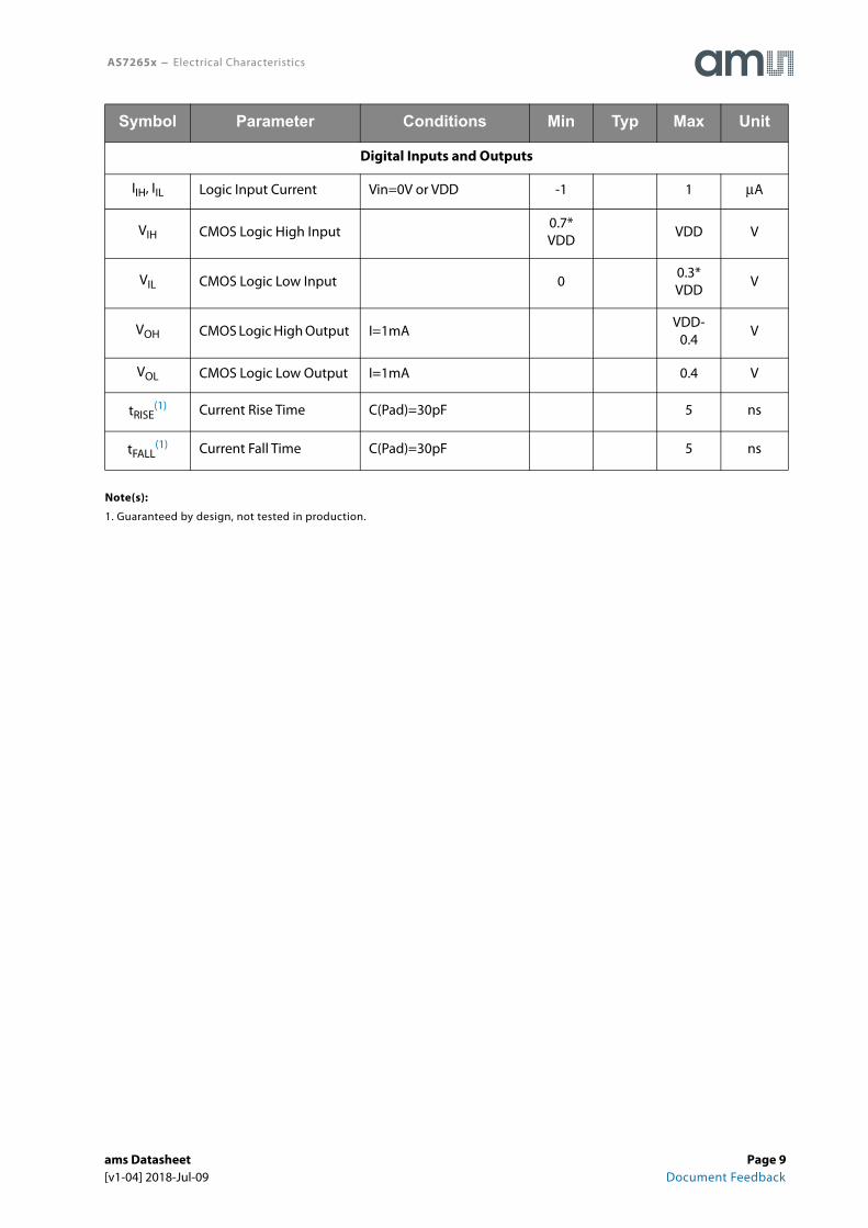
Note(s):
1. Guaranteed by design, not tested in production.
Digital Inputs and Outputs
IIH, IIL Logic Input Current Vin=0V or VDD -1 1 μA
VIH CMOS Logic High Input 0.7* VDD
VDD V
VIL CMOS Logic Low Input 00.3* VDD
V
VOH CMOS Logic High Output I=1mAVDD-
0.4V
VOL CMOS Logic Low Output I=1mA 0.4 V
tRISE(1) Current Rise Time C(Pad)=30pF 5 ns
tFALL(1) Current Fall Time C(Pad)=30pF 5 ns
Symbol Parameter Conditions Min Typ Max Unit
ams Datasheet Page 9[v1-04] 2018-Jul-09 Document Feedback
AS7265x − Electrical Characteristics
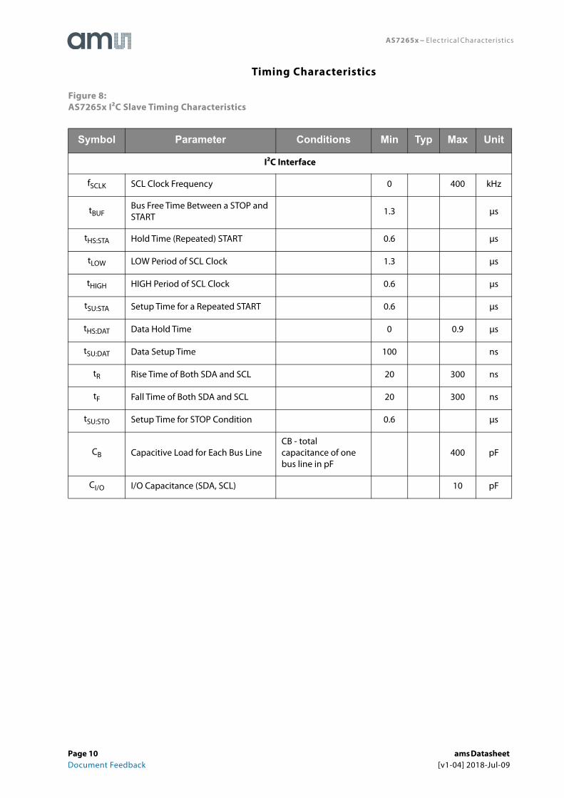
Timing Characteristics
Figure 8:AS7265x I²C Slave Timing Characteristics
Symbol Parameter Conditions Min Typ Max Unit
I²C Interface
fSCLK SCL Clock Frequency 0 400 kHz
tBUFBus Free Time Between a STOP and START
1.3 μs
tHS:STA Hold Time (Repeated) START 0.6 μs
tLOW LOW Period of SCL Clock 1.3 μs
tHIGH HIGH Period of SCL Clock 0.6 μs
tSU:STA Setup Time for a Repeated START 0.6 μs
tHS:DAT Data Hold Time 0 0.9 μs
tSU:DAT Data Setup Time 100 ns
tR Rise Time of Both SDA and SCL 20 300 ns
tF Fall Time of Both SDA and SCL 20 300 ns
tSU:STO Setup Time for STOP Condition 0.6 μs
CB Capacitive Load for Each Bus LineCB - total capacitance of one bus line in pF
400 pF
CI/O I/O Capacitance (SDA, SCL) 10 pF
Page 10 ams Datasheet Document Feedback [v1-04] 2018-Jul-09
AS7265x − Electrical Characteristics
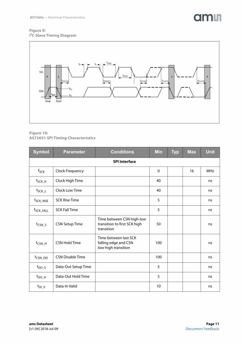
Figure 9:I²C Slave Timing Diagram
Figure 10:AS72651 SPI Timing Characteristics
Symbol Parameter Conditions Min Typ Max Unit
SPI Interface
fSCK Clock Frequency 0 16 MHz
tSCK_H Clock High Time 40 ns
tSCK_L Clock Low Time 40 ns
tSCK_RISE SCK Rise Time 5 ns
tSCK_FALL SCK Fall Time 5 ns
tCSN_S CSN Setup TimeTime between CSN high-low transition to first SCK high transition
50 ns
tCSN_H CSN Hold TimeTime between last SCK falling edge and CSN low-high transition
100 ns
tCSN_DIS CSN Disable Time 100 ns
tDO_S Data-Out Setup Time 5 ns
tDO_H Data-Out Hold Time 5 ns
tDI_V Data-In Valid 10 ns
SCL
SDA
tSU:STA
tLOW
tHIGH
tFtR
tHD:STA tSU:STOtSU:DATtHD:DAT
tBUF
VIH
VIL
P S S P
Stop Start
ams Datasheet Page 11[v1-04] 2018-Jul-09 Document Feedback

AS7265x − Electrical Characteristics
Figure 11:SPI Master Write Timing Diagram
Figure 12:SPI Master Read Timing Diagram
tDO_H
tCSN_H
CSN
MOSI
MISO
SCK
tCSN_S
MSB
tDO_S
LSB
HI-Z HI-Z
tCSN_DIS
tSCK_RISE tSCK_FALL
tDI_V
CSN_xx
MOSI
MISO
SCK
LSB
tSCK_H tSCK_L
Dont care
MSB
Page 12 ams Datasheet Document Feedback [v1-04] 2018-Jul-09

AS7265x − Typical Operating Characteristics
Optical CharacteristicsAll optical characteristics are optimized for diffused light. When using a point light source or collimated light on the sensor, the sensor opening must be covered by a lambertian diffuser with achromatic characteristics. Diffusor of Tsujiden like D121UP have been successfully tested at ams. If in the application diffused light, e.g. used by a reflective surface, no additional diffuser is required.
Figure 13:AS7265x LGA Average Field of View
Figure 14:AS7265x 18-Channel Spectral Responsivity
Typical Operating Characteristics
LGA Package SubstrateDIEEE
α = 12°H=2.5mm Sensor nssoor Lens
Diffused Light
β = 20.5°ββ == 20 520 5°
A=0.75mm
βββ
0
0.1
0.2
0.3
0.4
0.5
0.6
0.7
0.8
0.9
1
350
372
394
416
438
460
482
504
526
548
570
592
614
636
658
680
702
724
746
768
790
812
834
856
878
900
922
944
966
988
Nor
mal
ized
Resp
onsiv
ity
Wavelength (λ, nm)
18 Channel Spectral ResponseAS72651 + AS72652 + AS72653
410nm
435nm
460nm
485nm
510nm
535nm
560nm
585nm
610nm
645nm
680nm
705nm
730nm
760nm
810nm
860nm
900nm
940nm
ABCDEFGHRISJTUVWKL
ams Datasheet Page 13[v1-04] 2018-Jul-09 Document Feedback

AS7265x − Typical Operating Characteristics
Figure 15:AS72651 Spectral Responsivity
Figure 16:Optical Characteristics of AS72651 (Pass Band) (1)
Symbol Parameter Test Conditions Channel (nm) Min Typ Max Unit
R Channel R Incandescent(2),(4) 610 35(3),(4) counts/ (μW/cm2)
S Channel S Incandescent(2),(4) 680 35(3),(4) counts/ (μW/cm2)
T Channel T Incandescent(2),(4) 730 35(3),(4) counts/ (μW/cm2)
U Channel U Incandescent(2),(4) 760 35(3),(4) counts/ (μW/cm2)
V Channel V Incandescent(2),(4) 810 35(3),(4) counts/ (μW/cm2)
W Channel W Incandescent(2),(4) 860 35(3),(4) counts/ (μW/cm2)
FWHMFull Width Half Max
20 nm
WaccWavelength Accuracy
+10 -10 nm
0
0.2
0.4
0.6
0.8
1
1.2
350
370
390
410
430
450
470
490
510
530
550
570
590
610
630
650
670
690
710
730
750
770
790
810
830
850
870
890
910
930
950
970
990
Nor
mal
ized
Resp
onsiv
ity
Wavelength (λ, nm)
AS72651, 6-Channel Spectral Response
R610
S680
T730
U760
V810
W860
Page 14 ams Datasheet Document Feedback [v1-04] 2018-Jul-09

AS7265x − Typical Operating Characteristics
Note(s):
1. Calibration and measurements are made using diffused light.
2. Each channel is tested with GAIN = 16x, Integration Time (INT_T) = 166ms and VDD = VDD1 = VDD2 = 3.3V, TAMB=25°C.
3. The accuracy of the channel counts/μW/cm2 is ±12%.
4. The light source is an incandescent light with an irradiance of ~1500μW/cm2 (300-1000nm).
Figure 17:AS72652 Spectral Responsivity
darkDark Channel Counts
GAIN=64, TAMB=25°Ctint=165ms
5 counts
AFOVAverage Field of View
±20.5 deg
Symbol Parameter Test Conditions Channel (nm) Min Typ Max Unit
0
0.2
0.4
0.6
0.8
1
1.2
350
368
386
404
422
440
458
476
494
512
530
548
566
584
602
620
638
656
674
692
710
728
746
764
782
800
818
836
854
872
890
908
926
944
962
980
998
Nor
mal
ized
Resp
onsiv
ity
Wavelength (λ, nm)
AS72652, 6-Channel Spectral Response(w/AS72651 as Controller)
G560
H585
I645
J705
K900
L940
ams Datasheet Page 15[v1-04] 2018-Jul-09 Document Feedback
AS7265x − Typical Operating Characteristics
Page 16 ams Datasheet
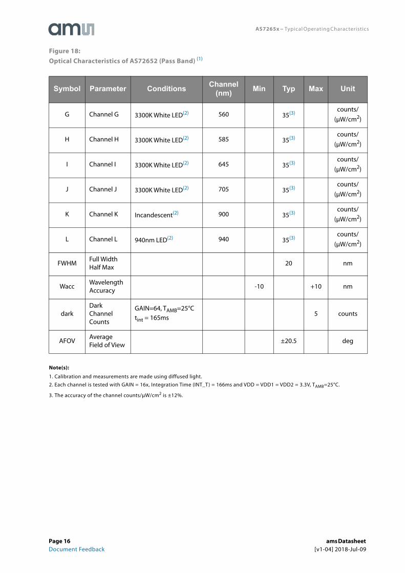
Figure 18:Optical Characteristics of AS72652 (Pass Band) (1)
Note(s):
1. Calibration and measurements are made using diffused light.
2. Each channel is tested with GAIN = 16x, Integration Time (INT_T) = 166ms and VDD = VDD1 = VDD2 = 3.3V, TAMB=25°C.
3. The accuracy of the channel counts/μW/cm2 is ±12%.
Symbol Parameter Conditions Channel (nm) Min Typ Max Unit
G Channel G 3300K White LED(2) 560 35(3) counts/ (μW/cm2)
H Channel H 3300K White LED(2) 585 35(3) counts/ (μW/cm2)
I Channel I 3300K White LED(2) 645 35(3) counts/ (μW/cm2)
J Channel J 3300K White LED(2) 705 35(3) counts/ (μW/cm2)
K Channel K Incandescent(2) 900 35(3) counts/ (μW/cm2)
L Channel L 940nm LED(2) 940 35(3) counts/ (μW/cm2)
FWHMFull Width Half Max
20 nm
WaccWavelength Accuracy
-10 +10 nm
darkDark Channel Counts
GAIN=64, TAMB=25°Ctint = 165ms
5 counts
AFOVAverage Field of View
±20.5 deg
Document Feedback [v1-04] 2018-Jul-09

AS7265x − Typical Operating Characteristics
Figure 19:AS72653 Spectral Responsivity
0
0.2
0.4
0.6
0.8
1
1.235
036
838
640
442
244
045
847
649
451
253
054
856
658
460
262
063
865
667
469
271
072
874
676
478
280
081
883
685
487
289
090
892
694
496
298
099
8
Nor
mal
ized
Resp
onsiv
ity
Wavelength (λ, nm)
AS72653, 6-Channel Spectral Response(w/AS72651 as controller)
A410
B435
C460
D485
E510
F535
ams Datasheet Page 17[v1-04] 2018-Jul-09 Document Feedback
AS7265x − Typical Operating Characteristics
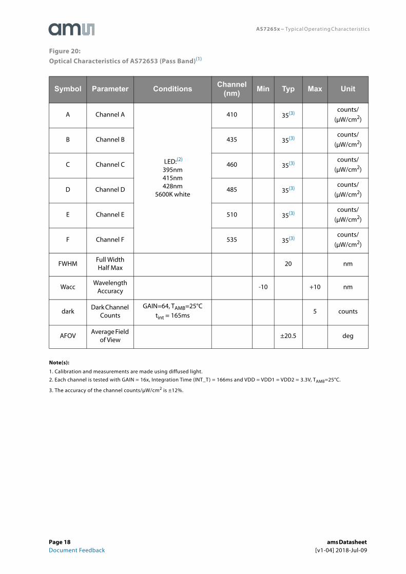
Figure 20:Optical Characteristics of AS72653 (Pass Band)(1)
Note(s):
1. Calibration and measurements are made using diffused light.
2. Each channel is tested with GAIN = 16x, Integration Time (INT_T) = 166ms and VDD = VDD1 = VDD2 = 3.3V, TAMB=25°C.
3. The accuracy of the channel counts/μW/cm2 is ±12%.
Symbol Parameter Conditions Channel (nm) Min Typ Max Unit
A Channel A
LED:(2)
395nm415nm428nm
5600K white
410 35(3) counts/ (μW/cm2)
B Channel B 435 35(3) counts/ (μW/cm2)
C Channel C 460 35(3) counts/ (μW/cm2)
D Channel D 485 35(3) counts/ (μW/cm2)
E Channel E 510 35(3) counts/ (μW/cm2)
F Channel F 535 35(3) counts/ (μW/cm2)
FWHMFull Width Half Max
20 nm
WaccWavelength
Accuracy-10 +10 nm
darkDark Channel
CountsGAIN=64, TAMB=25°C
tint = 165ms5 counts
AFOVAverage Field
of View±20.5 deg
Page 18 ams Datasheet Document Feedback [v1-04] 2018-Jul-09

AS7265x − Detailed Description
AS7265x 18-Channel Spectral_ID Detector OverviewEach of the three AS7265x Spectral_ID devices are next-gener-ation digital 6-channel spectral sensor devices. Each of the 6 channels has a Gaussian filter characteristic with a full width half maximum (FWHM) bandwidth of 20nm. The filters use an interference topology design providing high stability in terms of drift in time and temperature. The drifts are so small that it is undetectable in the measurement. The temperature drift of the device is largely determined by the drift of the sensor and the electronics. To compensate for the temperature drift in the application, every device of the AS7265x chipset includes an integrated temperature sensor.
Filter accuracy will be affected by the angle of incidence which itself is limited by integrated aperture and internal micro-lens structure. The aperture-limited average field of view is ±20.5° to deliver specified accuracy. All optical characteristics are optimized for using diffused light.
Each device contains an analog-to-digital converter (16-bit res-olution ADC) which integrates the current from each channel’s photodiode. Upon completion of the conversion cycle, the in-tegrated result is transferred to the corresponding data regis-ters. The transfers are double-buffered to ensure data integrity is maintained.
The external MCU interface control via I²C registers or AT com-mands, transparently controls the AS72652 and/or AS72653.
A serial flash is a required operating companion for this device and enables factory calibration/normalization of the filters. Supported device types are noted inOrdering & Contact Information at the end of this document. Required operating code can be downloaded at download.ams.com.
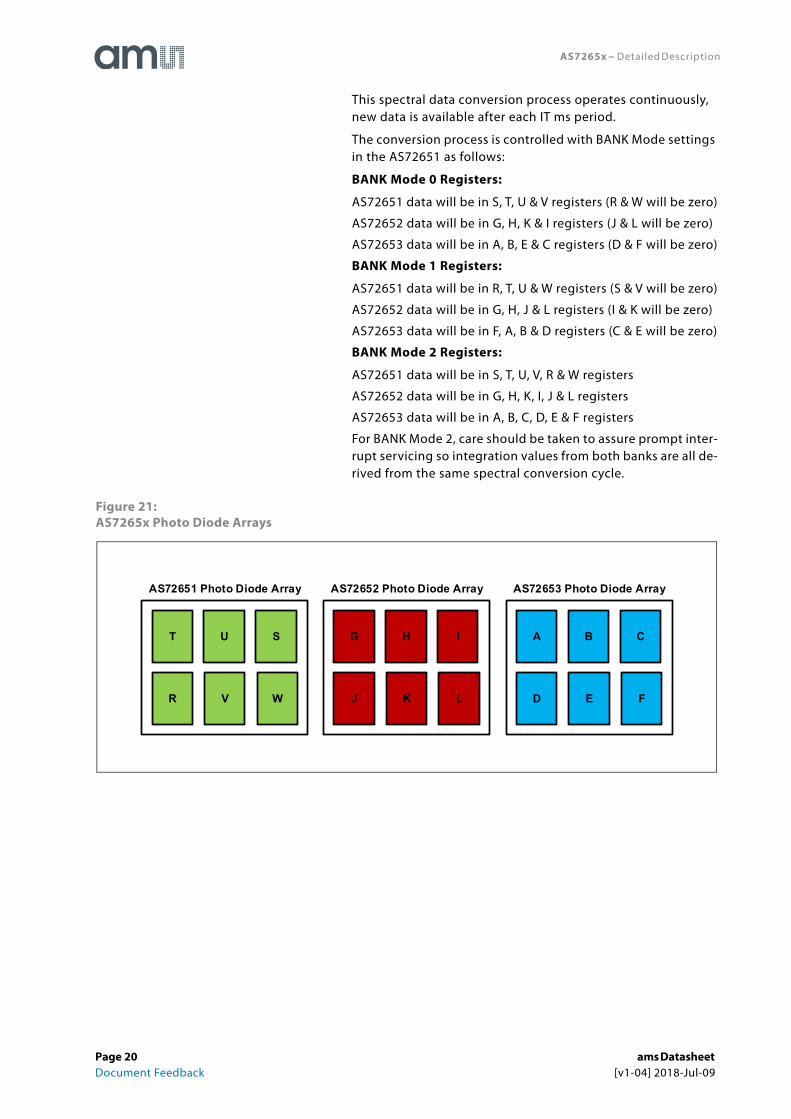
Channel Data Conversion of the AS7265x DevicesAll three of these 6 channel devices use conversion implement-ed via two photodiode banks in each device. Refer to Figure 21and Figure 22. Bank 1 consists of register data from 4 of the 6 photodiodes, with 2 registers zeroed and Bank 2 con-sists of data from a different set of 4 of the 6 photodiodes, with 2 different registers zeroed. Spectral conversion requires the integration time (IT in ms) set to complete. If both photodiode
banks are required to complete the conversion, the 2nd bank requires an additional IT ms. Minimum IT for a single bank con-version is 2.8 ms. If data is required from all 6 photodiodes then the device must perform 2 full conversions (2 x Integration Time).
Detailed Description
ams Datasheet Page 19[v1-04] 2018-Jul-09 Document Feedback
AS7265x − Detailed Description
This spectral data conversion process operates continuously, new data is available after each IT ms period.
The conversion process is controlled with BANK Mode settings in the AS72651 as follows:
BANK Mode 0 Registers:
AS72651 data will be in S, T, U & V registers (R & W will be zero)
AS72652 data will be in G, H, K & I registers (J & L will be zero)
AS72653 data will be in A, B, E & C registers (D & F will be zero)
BANK Mode 1 Registers:
AS72651 data will be in R, T, U & W registers (S & V will be zero)
AS72652 data will be in G, H, J & L registers (I & K will be zero)
AS72653 data will be in F, A, B & D registers (C & E will be zero)
BANK Mode 2 Registers:
AS72651 data will be in S, T, U, V, R & W registers
AS72652 data will be in G, H, K, I, J & L registers
AS72653 data will be in A, B, C, D, E & F registers
For BANK Mode 2, care should be taken to assure prompt inter-rupt servicing so integration values from both banks are all de-rived from the same spectral conversion cycle.
Figure 21:AS7265x Photo Diode Arrays
G H I
J K L
AS72652 Photo Diode Array
A B C
D E F
AS72653 Photo Diode Array
T U S
R V W
AS72651 Photo Diode Array
Page 20 ams Datasheet Document Feedback [v1-04] 2018-Jul-09

AS7265x − Detailed Description
Figure 22:Bank Mode and Data Conversion
RC OscillatorThe timing generation circuit consists of on-chip 16MHz, tem-perature compensated oscillators, which provide the individual master clocks of the AS7625x devices
Temperature SensorThe AS7265x internal temperature sensors are constantly mea-suring on-chip temperature to enable temperature compensa-tion procedures, and can be read via I²C registers or AT com-mands in the AS72651.
BANK Mode 0
One Conversion S, T, U, V, I, G, H, K, C, A, B, E Integration Time
R, T, U, W, L, G, H, J, F, A, B, DOne Conversion
BANK Mode 1
Integration Time
1st Conversion
BANK Mode 2
Integration Time
2nd Conversion
Integration Time
S, T, U, V, I, G, H, K, C, A, B, E
R, T, U, W, L, G, H, J, F, A, B, D
ams Datasheet Page 21[v1-04] 2018-Jul-09 Document Feedback

AS7265x − Detailed Description
ResetPulling down the RESN pin for longer than 100ms resets the AS72651 which proceed to reset the AS72562 and the same RESN signal shown below can be used directly to reset the AS72653.
Figure 23:Reset Circuit
AS7265x LED_IND ControlsThere are LED_IND pins on all AS7265x devices. An LED con-nected to LED_IND can be used as a general power indicator and will automatically be used to indicate a Flash firmware up-date is occurring.
The LED_IND can then be setup as needed. Each AS7265x LED_IND source can be turned on/off via AT commands or I²C register control, and LED_IND sink current is programmable to 1mA, 2mA, 4mA or 8mA. This LED_IND control can also be used in applications just like the LED_DRV control (described below), if the lower current sink of the LED_IND control is appropriate.
Electronic Shutter with AS7265x LED_DRV Driver ControlThere are LED_DRV pins on all AS7265x devices. The LED_DRV pin can be used to control external LED sources as needed for sensor applications. LED_DRV can sink a programmable current of 12.5mA, 25mA, 50mA or 100mA. The control can be turned on/off via I²C registers or AT commands, and as such it provides the AS7265x device with an electronic shutter.
Interrupt OperationInterrupt operation is only needed for AS72651 as it transpar-ently controls data collection from the AS72652 (if used) or AS72653 (if used).
Reset
AS72651
Spectral_ID Engine
RESN
Push > 100ms
VDD
Page 22 ams Datasheet Document Feedback [v1-04] 2018-Jul-09

AS7265x − Detailed Description
ams Datasheet Page 23
If BANK is set in the AS72651 to Mode 0 or Mode 1, data is ready
after the 1st integration time. If BANK is set to Mode 2, data is ready after two integration times.
For interrupt operation using I²C registers, if interrupts are en-abled and data is ready, the INT pin is set low and DATA_RDY is set to 1. Reading the raw or calibration data releases (returns high) the interrupt. For multi-byte sensor data (2 or 4 bytes), after the 1st byte is read the remaining bytes are shadow pro-tected in case an integration cycle completes just after the 1st byte is read. The sensors continue to gather information at the rate of the integration time, hence if the sensor registers are not read when the interrupt line goes low, it will stay low and the next cycle’s sensor data will be available in the registers at the end of the next integration cycle.
For interrupt operation using AT Commands, if interrupts are enabled and data is ready the INT pin is set low and is released (returns high) after any sensor data is read.
Required Flash MemorySerial flash is a required operating companion for this device, and enables the I²C and UART interfaces, as well as enabling calibrated data results. Supported device types are noted in Ordering & Contact Information at the end of this document. Required operating code can be downloaded at download.ams.com.
I²C Slave InterfaceIf selected by the I2C_ENB pin setting, interface and control can be accomplished through an I²C compatible slave interface to a set of registers that provide access to device control functions and output data. These registers on the AS72651 are, in reality, implemented as virtual registers in software. The actual I²C slave hardware registers number only three and are described in the table below. The steps necessary to access the virtual registers defined in the following are explained in pseudocode for exter-nal I²C master writes and reads below.
I²C Feature List
• Fast mode (400kHz).
• 7+1-bit addressing mode.
• Write format: Byte.
• Read format: Byte.
• SDA input delay and SCL spike filtering by integrated RC-components.
[v1-04] 2018-Jul-09 Document Feedback

AS7265x − Detailed Description
Figure 24:I²C Slave Device Address and Physical Registers
I²C Virtual Register Write AccessI²C Virtual Resister Byte Write, detailed below, shows the pseudocode necessary to write virtual registers on the AS72651. Note that, because the actual registers of interest are realized as virtual registers, a means of indicating whether there is a pending read or write operation of a given virtual register is needed. To convey this information, the most significant bit of the virtual register address is used as a marker. If it is 1, then a write is pending, otherwise the slave is expecting a virtual read operation. The pseudocode illustrates the proper tech-nique for polling of the I²C slave status register to ensure the slave is ready for each transaction.
Entity Description Note
Device Slave Address 8-bit slave addressByte = 1001001x (device address = 49 hex)• x= 1 for Master Read (byte = 93 hex)• x= 0 for Master Write (byte = 92 hex)
STATUS RegisterI²C slave interface STATUS register. Read-only.
Register Address = 0x00Bit 1: TX_VALID • 0 - New data may be written to WRITE register• 1 -WRITE register occupied. Do NOT write.
Bit 0: RX_VALID• 0 -No data is ready to be read in READ register.• 1 -Data byte available in READ register.
WRITE RegisterI²C slave interface WRITE register. Write-only.
Register Address = 0x01• 8-Bits of data written by the I²C Master
intended for receipt by the I²C slave. Used for both virtual register addresses and write data.
READ RegisterI²C slave interface READ register. Read-only.
Register Address = 0x02• 8-Bits of data to be read by the I²C Master.
Page 24 ams Datasheet Document Feedback [v1-04] 2018-Jul-09
AS7265x − Detailed Description
I²C Virtual Register Byte WritePseudocode
Poll I²C slave STATUS register;
If TX_VALID bit is 0, a write can be performed on the interface;
Send a virtual register address and set the MSB of the register address to 1 to indicate the pending write;
Poll I²C slave STATUS register;
If TX_VALID bit is 0, the virtual register address for the write has been received and the data may now be written;
Write the data.
Sample Code:
#define I2C_AS72XX_SLAVE_STATUS_REG 0x00
#define I2C_AS72XX_SLAVE_WRITE_REG 0x01
#define I2C_AS72XX_SLAVE_READ_REG 0x02
#define I2C_AS72XX_SLAVE_TX_VALID 0x02
#define I2C_AS72XX_SLAVE_RX_VALID 0x01
void i2cm_AS72xx_write(uint8_t virtualReg, uint8_t d)
{
volatile uint8_tstatus;
while (1)
{
// Read slave I²C status to see if the write buffer is ready.
status = i2cm_read(I2C_AS72XX_SLAVE_STATUS_REG);
if ((status & I2C_AS72XX_SLAVE_TX_VALID) == 0)
// No inbound TX pending at slave. Okay to write now.
break ;
}
// Send the virtual register address (enabling bit 7 to indicate a write).
i2cm_write(I2C_AS72XX_SLAVE_WRITE_REG, (virtualReg | 0x80)) ;
while (1)
{
// Read the slave I²C status to see if the write buffer is ready.
status = i2cm_read(I2C_AS72XX_SLAVE_STATUS_REG) ;
if ((status & I2C_AS72XX_SLAVE_TX_VALID) == 0)
// No inbound TX pending at slave. Okay to write data now.
break ;
}
// Send the data to complete the operation.
i2cm_write(I2C_AS72XX_SLAVE_WRITE_REG, d) ;
}
I²C Virtual Register Read access
ams Datasheet Page 25[v1-04] 2018-Jul-09 Document Feedback

AS7265x − Detailed Description
Page 26 ams Datasheet
I²C Virtual Register Byte Read, detailed below, shows the pseudocode necessary to read virtual registers on the AS72651. Note that in this case, reading a virtual register, the register address is not modified.
I²C Virtual Register Byte ReadPseudocode
Poll I²C slave STATUS register;
If TX_VALID bit is 0, the virtual register address for the read may be written;
Send a virtual register address;
Poll I²C slave STATUS register;
If RX_VALID bit is 1, the read data is ready;
Read the data.
Sample Code
uint8_t i2cm_AS72xx_read(uint8_t virtualReg)
{
volatile uint8_t status, d;
while (1)
{
// Read slave I²C status to see if the read buffer is ready.
status = i2cm_read(I2C_AS72XX_SLAVE_STATUS_REG) ;
if ((status & I2C_AS72XX_SLAVE_TX_VALID) == 0)
// No inbound TX pending at slave. Okay to write now.
break;
}
// Send the virtual register address (disabling bit 7 to indicate a read).
i2cm_write(I2C_AS72XX_SLAVE_WRITE_REG, virtualReg);
while (1)
{
// Read the slave I²C status to see if our read data is available.
status = i2cm_read(I2C_AS72XX_SLAVE_STATUS_REG);
if ((status & I2C_AS72XX_SLAVE_RX_VALID)!= 0)
// Read data is ready.
break;
}
// Read the data to complete the operation.
d = i2cm_read(I2C_AS72XX_SLAVE_READ_REG) ;
return d;s
}
The details of the i2cm_read() and i2cm_write() functions in previous figures are dependent upon the nature and implemen-tation of the external I²C master device.
Document Feedback [v1-04] 2018-Jul-09
AS7265x − Detailed Description
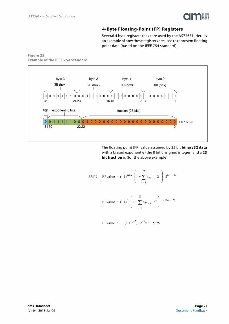
4-Byte Floating-Point (FP) RegistersSeveral 4 byte registers (hex) are used by the AS72651. Here is an example of how these registers are used to represent floating point data (based on the IEEE 754 standard).
Figure 25:Example of the IEEE 754 Standard
The floating point (FP) value assumed by 32 bit binary32 data with a biased exponent e (the 8 bit unsigned integer) and a 23 bit fraction is (for the above example):
0 0 1 1 1 1 1 031
0 0 1 0 0 0 0 0 0 0 0 0 0 0 0 0 0 0 0 0 0 0 0 0
3E (hex) 20 (hex) 00 (hex) 00 (hex)
byte 3 byte 2 byte 1 byte 0
0 0 1 1 1 1 1 0 0 0 1 0 0 0 0 0 0 0 0 0 0 0 0 0 0 0 0 0 0 0 0 0
exponent (8 bits) fraction (23 bits)
24 23 16 15 8 7 0
31 2330 22 0
sign
= 0.15625
(EQ1) FPvalue 1–( )sign 1 b23 i–
i 1–
23
2 i–⋅+
2 e 127–( )⋅ ⋅=
FPvalue 1–( )0 1 b23 i–
i 1–
23
2 i–⋅+
2 124 127–( )⋅ ⋅=
FPvalue 1 1 2 2–+( ) 2 3– 0.15625=⋅ ⋅=
ams Datasheet Page 27[v1-04] 2018-Jul-09 Document Feedback

AS7265x − Detailed Description
I²C Virtual Register SetThe figure below provides a summary of the AS72651 I²C regis-ter set for the AS72651 which serves as the master interface of the 3 device AS7265x set. Figures after that provide additional register details. All register data is hex, and all multi-byte enti-ties are Big Endian (most significant byte is situated at the low-est register address).
Multiple byte registers (2 byte integer, or, 4 byte floating point) must be read in the order of ascending register addresses (low to high) and if capable of being written to, must also be written in the order ascending register addresses.
Figure 26:AS72651 I²C Master Device Virtual Register Set Overview
Addr Name <D7> <D6> <D5> <D4> <D3> <D2> <D1> <D0>
0x00HW Version
HW Version H
0x01 HW Version L
0x02FW Version
FW Version H
0x03 FW Version L
0x04 Configuration SRST INT GAIN BANK DATA_RDY FRST
0x05 Integration Time Integration Time
0x06 Temperature Temperature
0x07LED
ConfigurationREAD_
ERRLED_DRV
ENA-BLELED
_DRVLED_INT
ENABLE LED_
INT
0x08 RAW value R, G, A RAW value H
0x09 RAW value R, G, A RAW value L
0x0A RAW value S, H, B RAW value H
0x0B RAW value S, H, B RAW value L
0x0C RAW value T, I, C RAW value H
0x0D RAW value T, I, C RAW value L
0x0E RAW value U, J, D RAW value H
0x0F RAW value U, J, D RAW value L
0x10 RAW value V, K, E RAW value H
0x11 RAW value V, K, E RAW value L
0x12 RAW value W, L, F RAW value H
0x13 RAW value W, L, F RAW value L
Page 28 ams Datasheet Document Feedback [v1-04] 2018-Jul-09
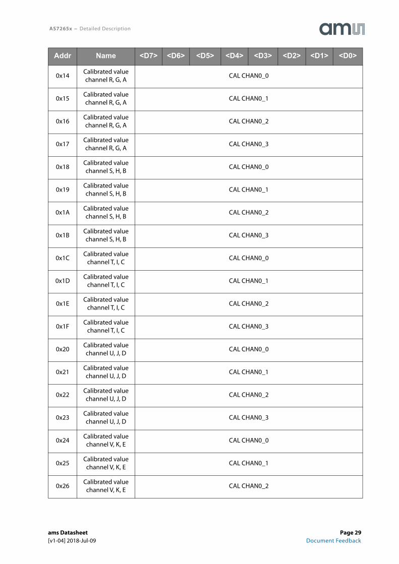
AS7265x − Detailed Description
0x14Calibrated value channel R, G, A
CAL CHAN0_0
0x15Calibrated value channel R, G, A
CAL CHAN0_1
0x16Calibrated value channel R, G, A
CAL CHAN0_2
0x17Calibrated value channel R, G, A
CAL CHAN0_3
0x18Calibrated value channel S, H, B
CAL CHAN0_0
0x19Calibrated value channel S, H, B
CAL CHAN0_1
0x1ACalibrated value channel S, H, B
CAL CHAN0_2
0x1BCalibrated value channel S, H, B
CAL CHAN0_3
0x1CCalibrated value
channel T, I, CCAL CHAN0_0
0x1DCalibrated value
channel T, I, CCAL CHAN0_1
0x1ECalibrated value
channel T, I, CCAL CHAN0_2
0x1FCalibrated value
channel T, I, CCAL CHAN0_3
0x20Calibrated value channel U, J, D
CAL CHAN0_0
0x21Calibrated value channel U, J, D
CAL CHAN0_1
0x22Calibrated value channel U, J, D
CAL CHAN0_2
0x23Calibrated value channel U, J, D
CAL CHAN0_3
0x24Calibrated value channel V, K, E
CAL CHAN0_0
0x25Calibrated value channel V, K, E
CAL CHAN0_1
0x26Calibrated value channel V, K, E
CAL CHAN0_2
Addr Name <D7> <D6> <D5> <D4> <D3> <D2> <D1> <D0>
ams Datasheet Page 29[v1-04] 2018-Jul-09 Document Feedback

AS7265x − Detailed Description
0x27Calibrated value channel V, K, E
CAL CHAN0_3
0x28Calibrated value channel W, L, F
CAL CHAN0_0
0x29Calibrated value channel W, L, F
CAL CHAN0_1
0x2ACalibrated value channel W, L, F
CAL CHAN0_2
0x2BCalibrated value channel W, L, F
CAL CHAN0_3
0x48 FW control START STOPBYTES_TRANSFERRED
LOCKSWITC
HBANK1 ERROR
CHKSUM
0x49 FW byte count FW_BYTE_COUNT_H
0x4A FW byte count FW_BYTE_COUNT_L
0x4B FW payload HW version H
0x4F DEV SELSecond
SlaveFirst Slave
SELECT DATA
0x50 COEF DATA COEF_DATA_0
0x51 COEF DATA COEF_DATA_1
0x52 COEF DATA COEF_DATA_2
0x53 COEF DATA COEF_DATA_3
0x54 COEF READ COEF_READ
0x55 COEF WRITE COEF_WRITE
Addr Name <D7> <D6> <D5> <D4> <D3> <D2> <D1> <D0>
Page 30 ams Datasheet Document Feedback [v1-04] 2018-Jul-09
AS7265x − Detailed Description
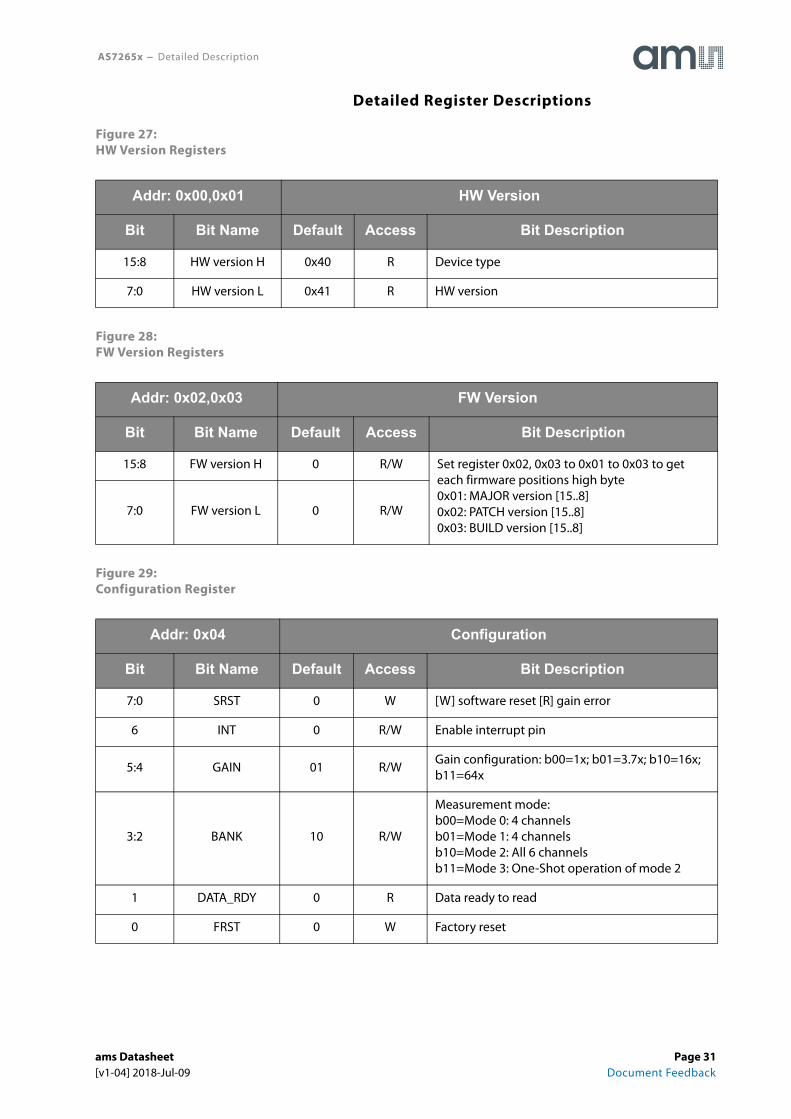
Detailed Register Descriptions
Figure 27:HW Version Registers
Figure 28:FW Version Registers
Figure 29:Configuration Register
Addr: 0x00,0x01 HW Version
Bit Bit Name Default Access Bit Description
15:8 HW version H 0x40 R Device type
7:0 HW version L 0x41 R HW version
Addr: 0x02,0x03 FW Version
Bit Bit Name Default Access Bit Description
15:8 FW version H 0 R/W Set register 0x02, 0x03 to 0x01 to 0x03 to get each firmware positions high byte0x01: MAJOR version [15..8]0x02: PATCH version [15..8]0x03: BUILD version [15..8]
7:0 FW version L 0 R/W
Addr: 0x04 Configuration
Bit Bit Name Default Access Bit Description
7:0 SRST 0 W [W] software reset [R] gain error
6 INT 0 R/W Enable interrupt pin
5:4 GAIN 01 R/WGain configuration: b00=1x; b01=3.7x; b10=16x; b11=64x
3:2 BANK 10 R/W
Measurement mode: b00=Mode 0: 4 channelsb01=Mode 1: 4 channelsb10=Mode 2: All 6 channelsb11=Mode 3: One-Shot operation of mode 2
1 DATA_RDY 0 R Data ready to read
0 FRST 0 W Factory reset
ams Datasheet Page 31[v1-04] 2018-Jul-09 Document Feedback
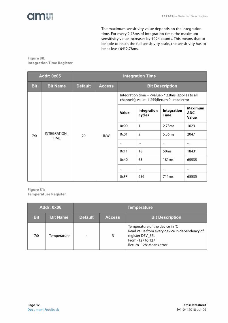
AS7265x − Detailed Description
The maximum sensitivity value depends on the integration time. For every 2.78ms of integration time, the maximum sensitivity value increases by 1024 counts. This means that to be able to reach the full sensitivity scale, the sensitivity has to be at least 64*2.78ms.
Figure 30:Integration Time Register
Figure 31:Temperature Register
Addr: 0x05 Integration Time
Bit Bit Name Default Access Bit Description
7:0INTEGRATION_
TIME20 R/W
Integration time = <value> * 2.8ms (applies to all channels); value: 1-255;Return 0 - read error
Value Integration Cycles
Integration Time
Maximum ADC Value
0x00 1 2.78ms 1023
0x01 2 5.56ms 2047
... ... ... ...
0x11 18 50ms 18431
0x40 65 181ms 65535
... ... ... ...
0xFF 256 711ms 65535
Addr: 0x06 Temperature
Bit Bit Name Default Access Bit Description
7:0 Temperature - R
Temperature of the device in °CRead value from every device in dependency of register DEV_SELFrom -127 to 127Return -128: Means error
Page 32 ams Datasheet Document Feedback [v1-04] 2018-Jul-09

AS7265x − Detailed Description
Figure 32:LED Configuration Register
Figure 33:RAW Value Channel R,G,A Register
Figure 34:RAW Value Channel S,H,B Register
Addr: 0x07 LED Configuration
Bit Bit Name Default Access Bit Description
7 READ_ERR 0 R Error while reading status
5:4 LED_DRV 00 R/WLED_DRV current limit: b00=12.5mA; b01=25mA; b10=50mA; b11=100mADevice depends on register DEV_SEL
3ENABLE LED_
DRV0 R/W
Enable LED DRVDevice depends on register DEV_SEL
2:1 LED_INT 01 R/WCurrent limit: b00=1mA; b01=2mA; b10=4mA; b11=8mADevice depends on register DEV_SEL
0ENABLE LED_
INT0 R/W
Enable LED INDDevice depends on register DEV_SEL
Addr: 0x08,0x09 RAW Value Channel R,G,A
Bit Bit Name Default Access Bit Description
15:8 RAW value H - RChannel R or J or D depends on register DEV_SEL
7:0 Raw value L - R
Addr: 0x0A,0x0B RAW Value Channel S,H,B
Bit Bit Name Default Access Bit Description
15:8 RAW value H - RChannel S or I or C depends on register DEV_SEL
7:0 Raw value L - R
ams Datasheet Page 33[v1-04] 2018-Jul-09 Document Feedback

AS7265x − Detailed Description
Figure 35:RAW Value Channel T,I,C Register
Figure 36:RAW Value Channel U,J,D Register
Figure 37:RAW Value Channel V,K,E Register
Figure 38:RAW Value Channel W,L,F Register
Addr: 0x0C/0x0D RAW Value Channel T,I,C
Bit Bit Name Default Access Bit Description
15:8 RAW value H - R Channel T or G or A depends on register DEV_SEL7:0 Raw value L - R
Addr: 0x0E,0x0F RAW Value Channel U,J,D
Bit Bit Name Default Access Bit Description
15:8 RAW value H - R Channel U or H or B depends on register DEV_SEL7:0 Raw value L - R
Addr: 0x10,0x011 RAW Value Channel V,K,E
Bit Bit Name Default Access Bit Description
15:8 RAW value H - RChannel V or K or E depends on register DEV_SEL
7:0 Raw value L - R
Addr: 0x12,0x013 RAW Value Channel W,L,F
Bit Bit Name Default Access Bit Description
15:8 RAW value H - R Channel W or L or F depends on register DEV_SEL7:0 Raw value L - R
Page 34 ams Datasheet Document Feedback [v1-04] 2018-Jul-09

AS7265x − Detailed Description
Figure 39:Calibrated Value Channel R,G,A Register
Figure 40:Calibrated Value Channel S, H, B Register
Figure 41:Calibrated Value Channel T, I, C Register
Addr: 0x17,0x016,0x15,0x014 Calibrated Value Channel R,G,A
Bit Bit Name Default Access Bit Description
31:24 CAL CHAN0_3 FF R
Channel R or J or D depends on register DEV_SEL
23:16 CAL CHAN0_2 FF R
15:8 CAL CHAN0_1 FF R
7:0 CAL CHAN0_0 FF R
Addr: 0x1B,0x01A,0x19,0x018 Calibrated Value Channel S,H,B
Bit Bit Name Default Access Bit Description
31:24 CAL CHAN1_3 FF R
Channel S or I or C depends on register DEV_SEL
23:16 CAL CHAN1_2 FF R
15:8 CAL CHAN1_1 FF R
7:0 CAL CHAN1_0 FF R
Addr: 0x1F,0x01E,0x1D,0x01C Calibrated Value Channel T,I,C
Bit Bit Name Default Access Bit Description
31:24 CAL CHAN2_3 FF R
Channel T or G or A depends on register DEV_SEL
23:16 CAL CHAN2_2 FF R
15:8 CAL CHAN2_1 FF R
7:0 CAL CHAN2_0 FF R
ams Datasheet Page 35[v1-04] 2018-Jul-09 Document Feedback

AS7265x − Detailed Description
Figure 42:Calibrated Value Channel U, J, D Register
Figure 43:Calibrated Value Channel V, K, E Register
Figure 44:Calibrated Value Channel W, L, F Register
Addr: 0x23,0x022,0x21,0x20 Calibrated Value Channel U,J,D
Bit Bit Name Default Access Bit Description
31:24 CAL CHAN3_3 FF R
Channel U or H or B depends on register DEV_SEL
23:16 CAL CHAN3_2 FF R
15:8 CAL CHAN3_1 FF R
7:0 CAL CHAN3_0 FF R
Addr: 0x27,0x026,0x25,0x24 Calibrated Value Channel V,K,E
Bit Bit Name Default Access Bit Description
31:24 CAL CHAN4_3 FF R
Channel V or K or E depends on register DEV_SEL
23:16 CAL CHAN4_2 FF R
15:8 CAL CHAN4_1 FF R
7:0 CAL CHAN4_0 FF R
Addr: 0x2B,0x02A,0x29,0x28 Calibrated Value Channel W,L,F
Bit Bit Name Default Access Bit Description
31:24 CAL CHAN5_3 FF R
Channel W or L or F depends on register DEV_SEL
23:16 CAL CHAN5_2 FF R
15:8 CAL CHAN5_1 FF R
7:0 CAL CHAN5_0 FF R
Page 36 ams Datasheet Document Feedback [v1-04] 2018-Jul-09

AS7265x − Detailed Description
Figure 45:FW Control Register
Figure 46:FW Byte Count Register
Figure 47:FW Payload Register
Addr: 0x48 FW Control
Bit Bit Name Default Access Bit Description
7 START R/W Set bit once to configure the device update
6 STOP W Reset firmware update state machine
5BYTES_
TRANSFERREDR All 56kbytes are transferred
4 LOCK R/W Lock this firmware for the next start
3 SWITCH W Switch between both firmware
2 BANK1 R Set if bank 1 is active, else bank 2
1 ERROR R Error occurred while firmware update
0 CHKSUM R Checksum of other bank is valid
Addr: 0x49,0x4A FW Byte Count
Bit Bit Name Default Access Bit Description
15:8FW_BYTE_COUNT_H
0 R
Byte counter of transferred image
7:0FW_BYTE_COUNT_L
R
Addr:0x4B FW Payload
Bit Bit Name Default Access Bit Description
7:0 HW version H 0 R/W Transfer of firmware byte
ams Datasheet Page 37[v1-04] 2018-Jul-09 Document Feedback
AS7265x − Detailed Description
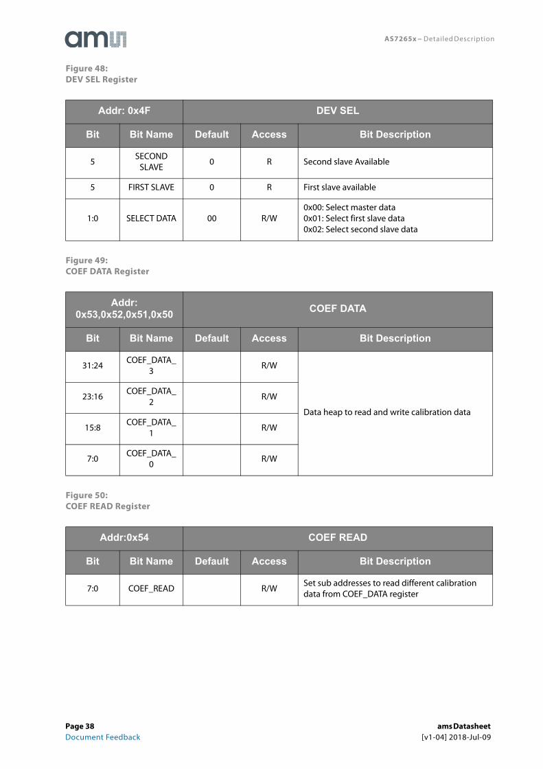
Figure 48:DEV SEL Register
Figure 49:COEF DATA Register
Figure 50:COEF READ Register
Addr: 0x4F DEV SEL
Bit Bit Name Default Access Bit Description
5SECOND
SLAVE0 R Second slave Available
5 FIRST SLAVE 0 R First slave available
1:0 SELECT DATA 00 R/W0x00: Select master data0x01: Select first slave data0x02: Select second slave data
Addr: 0x53,0x52,0x51,0x50 COEF DATA
Bit Bit Name Default Access Bit Description
31:24COEF_DATA_
3R/W
Data heap to read and write calibration data
23:16COEF_DATA_
2R/W
15:8COEF_DATA_
1R/W
7:0COEF_DATA_
0R/W
Addr:0x54 COEF READ
Bit Bit Name Default Access Bit Description
7:0 COEF_READ R/WSet sub addresses to read different calibration data from COEF_DATA register
Page 38 ams Datasheet Document Feedback [v1-04] 2018-Jul-09

AS7265x − Detailed Description
Figure 51:COEF WRITE Register
AS72651 I2C Firmware (FW) Update Procedure
• In the FW Update Control register set the Start_XFR bit to 1.
• Write 56k of data to the FW Download register starting with the first byte in the ams file, then proceed the end of the ams 56k file with consecutive writes.
• If desired read the FW Byte Count registers to see which byte is expected to be written next into the FW Download register.
• When the download file is completely written, confirm the action by using the FW Update Control register bit XFR_56k (should =1 if 56k has been downloaded).
• In the FW Update Control register, set the Toggle bit to 1 which will reboot the AS72651 with the new FW after checking the new FW for correct CRC. If the CRC is incorrect the toggle bit will not change and the new FW will not be used.
Figure 52:Firmware Byte Count High Byte
Addr:0x55 COEF WRITE
Bit Bit Name Default Access Bit Description
7:0 COEF_WRITE R/WSet sub addresses to write different calibration data from COEF_DATA register to persistent memory
Addr: 0x60/0xE0 Control_Setup
Bit Bit Name Default Access Bit Description
7 Start_XFR 0 R/W Set to 1 to start firmware update
6 Kill_XFR 0 R/W Set to 1 to stop firmware update.
5 XFR_56K 0 R Set to 1 when 56k bytes have been downloaded.
4 Reserved Reserved, do not use.
3 Toggle 0 R/W Set to 1 to toggle firmware image partition.
2:0 Reserved Reserved, do not use.
ams Datasheet Page 39[v1-04] 2018-Jul-09 Document Feedback
AS7265x − Detailed Description
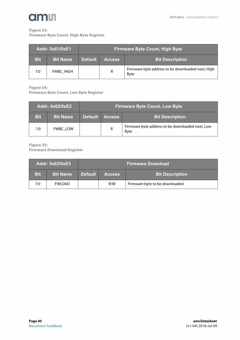
Figure 53:Firmware Byte Count, High Byte Register
Figure 54:Firmware Byte Count, Low Byte Register
Figure 55:Firmware Download Register
Addr: 0x61/0xE1 Firmware Byte Count, High Byte
Bit Bit Name Default Access Bit Description
7:0 FWBC_HIGH RFirmware byte address to be downloaded next, High Byte
Addr: 0x62/0xE2 Firmware Byte Count, Low Byte
Bit Bit Name Default Access Bit Description
7:0 FWBC_LOW RFirmware byte address to be downloaded next, Low Byte
Addr: 0x63/0xE3 Firmware Download
Bit Bit Name Default Access Bit Description
7:0 FWLOAD R/W Firmware byte to be downloaded
Page 40 ams Datasheet Document Feedback [v1-04] 2018-Jul-09
AS7265x − Detailed Description
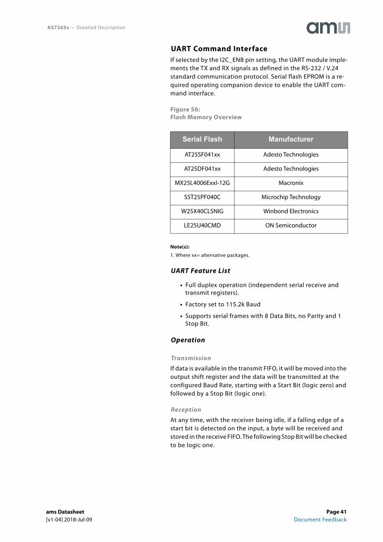
UART Command InterfaceIf selected by the I2C_ENB pin setting, the UART module imple-ments the TX and RX signals as defined in the RS-232 / V.24 standard communication protocol. Serial flash EPROM is a re-quired operating companion device to enable the UART com-mand interface.
Figure 56:Flash Memory Overview
Note(s):
1. Where xx= alternative packages.
UART Feature List
• Full duplex operation (independent serial receive and transmit registers).
• Factory set to 115.2k Baud
• Supports serial frames with 8 Data Bits, no Parity and 1 Stop Bit.
Operation
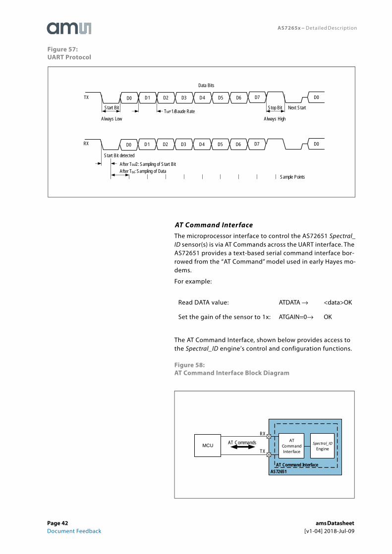
Transmission
If data is available in the transmit FIFO, it will be moved into the output shift register and the data will be transmitted at the configured Baud Rate, starting with a Start Bit (logic zero) and followed by a Stop Bit (logic one).
Reception
At any time, with the receiver being idle, if a falling edge of a start bit is detected on the input, a byte will be received and stored in the receive FIFO. The following Stop Bit will be checked to be logic one.
Serial Flash Manufacturer
AT25SF041xx Adesto Technologies
AT25DF041xx Adesto Technologies
MX25L4006ExxI-12G Macronix
SST25PF040C Microchip Technology
W25X40CLSNIG Winbond Electronics
LE25U40CMD ON Semiconductor
ams Datasheet Page 41[v1-04] 2018-Jul-09 Document Feedback
AS7265x − Detailed Description
Figure 57:UART Protocol
AT Command InterfaceThe microprocessor interface to control the AS72651 Spectral_ID sensor(s) is via AT Commands across the UART interface. The AS72651 provides a text-based serial command interface bor-rowed from the “AT Command” model used in early Hayes mo-dems.
For example:
The AT Command Interface, shown below provides access to the Spectral_ID engine’s control and configuration functions.
Figure 58:AT Command Interface Block Diagram
Read DATA value: ATDATA → <data>OK
Set the gain of the sensor to 1x: ATGAIN=0→ OK
Start Bit
TX D0 D1 D2 D3 D4 D5 D6 D7 D0
D0 D1 D2 D3 D4 D5 D6 D7 D0
Tbit=1/Baude RateStop Bit Next Start
Sample Points
Start Bit detected
After Tbit/2: Sampling of Start BitAfter Tbit: Sampling of Data
RX
Always Low Always High
Data Bits
AT Command Interface
Spectral_ID Engine
AT Command Interface
RX
MCUTX
AS72651
AT Command Interface
AT Commands
Page 42 ams Datasheet Document Feedback [v1-04] 2018-Jul-09
AS7265x − Detailed Description
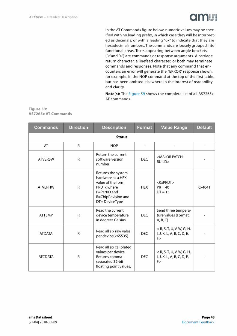
In the AT Commands figure below, numeric values may be spec-ified with no leading prefix, in which case they will be interpret-ed as decimals, or with a leading “0x” to indicate that they are hexadecimal numbers. The commands are loosely grouped into functional areas. Texts appearing between angle brackets (‘<‘and ‘>‘) are commands or response arguments. A carriage return character, a linefeed character, or both may terminate commands and responses. Note that any command that en-counters an error will generate the “ERROR” response shown, for example, in the NOP command at the top of the first table, but has been omitted elsewhere in the interest of readability and clarity.
Note(s): The Figure 59 shows the complete list of all AS7265x AT commands.
Figure 59:AS7265x AT Commands
Commands Direction Description Format Value Range Default
Status
AT R NOP - - -
ATVERSW RReturn the current software version number
DEC<MAJOR.PATCH.BUILD>
-
ATVERHW R
Returns the system hardware as a HEX value of the form PRDTx where P=PartID and R=ChipRevision and DT= DeviceType
HEX<0xPRDT>PR = 40DT = 15
0x4041
ATTEMP RRead the current device temperature in degrees Celsius
DECSend three tempera-ture values (Format: A, B, C)
-
ATDATA RRead all six raw vales per device(<65535)
DEC< R, S, T, U, V, W, G, H, I, J, K, L, A, B, C, D, E, F>
-
ATCDATA R
Read all six calibrated values per device.Returns comma- separated 32-bit floating point values.
DEC< R, S, T, U, V, W, G, H, I, J, K, L, A, B, C, D, E, F>
-
ams Datasheet Page 43[v1-04] 2018-Jul-09 Document Feedback
AS7265x − Detailed Description
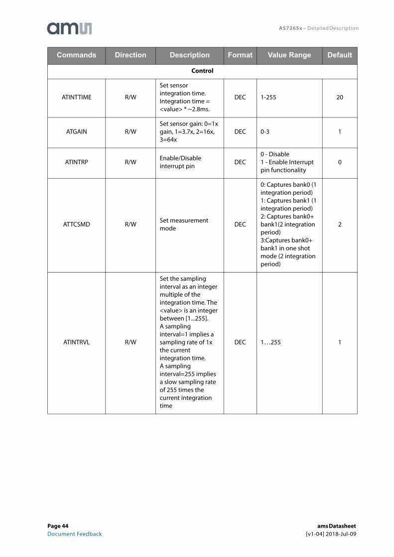
Control
ATINTTIME R/W
Set sensor integration time. Integration time = <value> * ~2.8ms.
DEC 1-255 20
ATGAIN R/WSet sensor gain: 0=1x gain, 1=3.7x, 2=16x, 3=64x
DEC 0-3 1
ATINTRP R/WEnable/Disable interrupt pin
DEC0 - Disable1 - Enable Interrupt pin functionality
0
ATTCSMD R/WSet measurement mode
DEC
0: Captures bank0 (1 integration period)1: Captures bank1 (1 integration period)2: Captures bank0+ bank1(2 integration period)3:Captures bank0+ bank1 in one shot mode (2 integration period)
2
ATINTRVL R/W
Set the sampling interval as an integer multiple of the integration time. The <value> is an integer between [1...255].A sampling interval=1 implies a sampling rate of 1x the current integration time.A sampling interval=255 implies a slow sampling rate of 255 times the current integration time
DEC 1…255 1
Commands Direction Description Format Value Range Default
Page 44 ams Datasheet Document Feedback [v1-04] 2018-Jul-09

AS7265x − Detailed Description
ATBURST R/W
Sends a number of calibrated data without separate requests second parameter for the burst mode is optionally format: Send: ATBURST=10,0 or ATBURST=10Read: ATBURST ≥ 10,0 OK
DEC
BURST NUMBER:0 - Burst mode is deactivated1-254 - Number of burst transfers255 - Send unlimited bursts (stops with ATBURST=0)
BURST MODE:0 - Raw values (default, like ATDATA)1 - Calibrated values (like ATCDATA)
0
ATLED0 R/WEnables or disables the indication LED
DEC0 - LED off 1 - LED on
1
ATLED1 R/WEnables or disables the driver LED
DEC0 - LED off 1 - LED on
0
ATLED2 R/WEnables or disables the indication LED for first I2C slave
DEC0 - LED off 1 - LED on
1
ATLED3 R/WEnables or disables the driver LED for first I2C slave
DEC0 - LED off 1 - LED on
0
ATLED4 R/WEnables or disables the indication LED for second I2C slave
DEC0 - LED off 1 - LED on
1
ATLED5 R/WEnables or disables the driver LED for second I2C slave
DEC0 - LED off 1 - LED on
0
ATLEDC R/WSets LED_IND and LED_DRV current(for master only)
HEX
[1...0] LED_IND: b00=1mA; b01=2mA; b10=4mA; b11=8mA[5...4] LED_DRV: b00=12.5mA; b01=25mA; b10=50mA; b11=100mA
0x00
Commands Direction Description Format Value Range Default
ams Datasheet Page 45[v1-04] 2018-Jul-09 Document Feedback
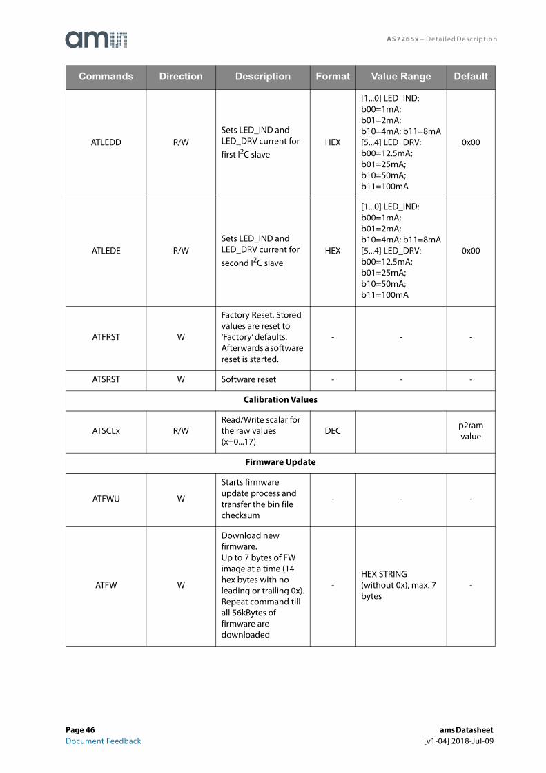
AS7265x − Detailed Description
ATLEDD R/WSets LED_IND and LED_DRV current for first I2C slave
HEX
[1...0] LED_IND: b00=1mA; b01=2mA; b10=4mA; b11=8mA[5...4] LED_DRV: b00=12.5mA; b01=25mA; b10=50mA; b11=100mA
0x00
ATLEDE R/WSets LED_IND and LED_DRV current for second I2C slave
HEX
[1...0] LED_IND: b00=1mA; b01=2mA; b10=4mA; b11=8mA[5...4] LED_DRV: b00=12.5mA; b01=25mA; b10=50mA; b11=100mA
0x00
ATFRST W
Factory Reset. Stored values are reset to ‘Factory’ defaults. Afterwards a software reset is started.
- - -
ATSRST W Software reset - - -
Calibration Values
ATSCLx R/WRead/Write scalar for the raw values (x=0...17)
DECp2ram value
Firmware Update
ATFWU W
Starts firmware update process and transfer the bin file checksum
- - -
ATFW W
Download new firmware.Up to 7 bytes of FW image at a time (14 hex bytes with no leading or trailing 0x).Repeat command till all 56kBytes of firmware are downloaded
-HEX STRING (without 0x), max. 7 bytes
-
Commands Direction Description Format Value Range Default
Page 46 ams Datasheet Document Feedback [v1-04] 2018-Jul-09
AS7265x − Detailed Description
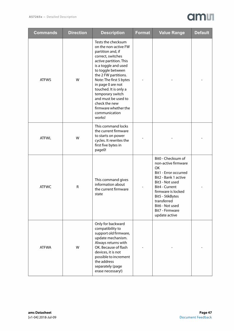
ATFWS W
Tests the checksum on the non-active FW partition and, if correct, switches active partition. This is a toggle and used to toggle between the 2 FW partitions. Note: The first 5 bytes in page 0 are not touched. It is only a temporary switch and must be used to check the new firmware whether the communication works!
- - -
ATFWL W
This command locks the current firmware to starts on power cycles. It rewrites the first five bytes in page0!
- - -
ATFWC R
This command gives information about the current firmware state
-
Bit0 - Checksum of non-active firmware OKBit1 - Error occurredBit2 - Bank 1 activeBit3 - Not usedBit4 - Current firmware is lockedBit5 - 56kBytes transferredBit6 - Not usedBit7 - Firmware update active
-
ATFWA W
Only for backward compatibility to support old firmware, update mechanism. Always returns with OK. Because of flash devices, it is not possible to increment the address separately (page erase necessary!)
- - -
Commands Direction Description Format Value Range Default
ams Datasheet Page 47[v1-04] 2018-Jul-09 Document Feedback
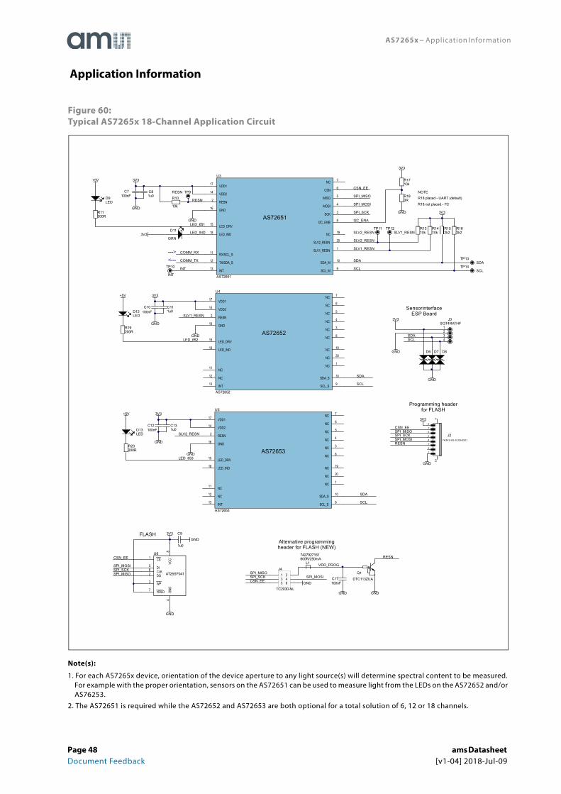
AS7265x − Application Information
Figure 60:Typical AS7265x 18-Channel Application Circuit
Note(s):
1. For each AS7265x device, orientation of the device aperture to any light source(s) will determine spectral content to be measured. For example with the proper orientation, sensors on the AS72651 can be used to measure light from the LEDs on the AS72652 and/or AS76253.
2. The AS72651 is required while the AS72652 and AS72653 are both optional for a total solution of 6, 12 or 18 channels.
Application Information
GND
CSN_EESPI_MISOSPI_SCKSPI_MOSIRESN
3V3
Programming headerfor FLASH
GND
4
HOLD7WP3
VCC
8
DO2 CLK6 DI5CS1
U6
AT25SF041
C9
1u0
GND
3V3
GND
SPI_MOSI
SPI_MISOSPI_SCK
COMM_TX
COMM_RX---><---
SPI_MOSI
SPI_MISO
SPI_SCK
CSN_EE
CSN_EE
R10
10k
C7
100nFC81u0
C10
100nF
C12
100nF
C111u0
C131u0
GND
GND
GND
GND
GND
GND
1234
J3SQT4RATHF
GND
SDA
SDA
SLV1_RESN
SLV2_RESN
SCL
SCL
3V3
3V3
R152k2
R162k2
SDA
SDA
SCL
SCL
3V3
D6 D7 D8
GND
R1710k
3V3
INT
SLV1_RESN
R11200R
+5V
TP9RESN
TP10
INT
TP11SLV2_RESN
TP12SLV1_RESN
TP13SDA
TP14SCL
R180R
GND
D9LED
D12LED
D13LED
R23200R
R19200R
+5V
+5V
D11
GRN
RESN
FH34S-8S-0.5SH(50)
1
2
3
4
5
610
9
7
8
J2SLV2_RESN
AS72652
LED_IND18
VDD117
GND16
LED_DRV15
NC 1NC 20NC 19
VDD214
NC 3
NC 6
RESN2
INT13
NC 4
NC 7
SDA_S 10NC11
NC 5
NC 8
NC12
SCL_S 9
U4
AS72652
AS72653
LED_IND18
VDD117
GND16
LED_DRV15
NC 1NC 20NC 19
VDD214
NC 3
NC 6
RESN2
INT13
NC 4
NC 7
SDA_S 10NC11
NC 5
NC 8
NC12
SCL_S 9
U5
AS72653
AS72651
LED_IND18
VDD117
GND16
LED_DRV15
SLV1_RESN 1SLV2_RESN 20
NC 19
VDD214
SCK 3
CSN 6
RESN2
INT13
MOSI 4
NC 7
SDA_M 10RX/SCL_S11
MISO 5
I2C_ENB 8
TX/SDA_S12
SCL_M 9
U3
AS72651
3V3
3V3
3V3
R1310k
R1410k
I2C_ENA
FLASH
SPI_MOSISPI_SCKSPI_MISO
CSN_EEGND
1 23 45 6
J4
TC2030-NL
VDD_PROG
GND
7427927161
L1600R/250mA
Alternative programmingheader for FLASH (NEW)
SensorinterfaceESP Board
Q1
DTC113ZUA
GND
RESN
C17
100nF
LED_651
LED_652
LED_IND
LED_653
R18 placed - UART (default)
R18 not placed - I²C
NOTE
Page 48 ams Datasheet Document Feedback [v1-04] 2018-Jul-09

AS7265x − Package Drawings & Markings
Figure 61:Package Drawing
Note(s):
1. All dimensions are in millimeters.
2. XXXXX = tracecode.
3. Unless otherwise specified tolerances are: Angular (±.5°), Two Place Decimal (±.1), Three Place Decimal (±.05).
4. Contact finish is Au.
5. This package contains no lead (Pb).
6. This drawing is subject to change without notice.
Package Drawings & Markings
Green
RoHS
ams Datasheet Page 49[v1-04] 2018-Jul-09 Document Feedback

AS7265x − PCB Pad Layout
Suggested PCB pad layout guidelines for the LGA device are shown. Flash Gold is recommended as a surface finish for the landing pads.
Figure 62:Recommended PCB Pad Layout (Top View)
Note(s):
1. Unless otherwise specified, all dimensions are in millimeters.
2. Add 0.05mm all around the nominal lead width and length for the PCB pad land pattern.
3. This drawing is subject to change without notice.
PCB Pad Layout
4.05
3.85
Unit: mm
1
5
0.55
0.400.65
Page 50 ams Datasheet Document Feedback [v1-04] 2018-Jul-09
AS7265x − PCB Pad Layout
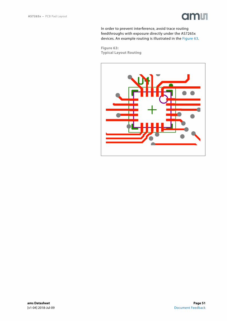
In order to prevent interference, avoid trace routing feedthroughs with exposure directly under the AS7265x devices. An example routing is illustrated in the Figure 63.
Figure 63:Typical Layout Routing
ams Datasheet Page 51[v1-04] 2018-Jul-09 Document Feedback

AS7265x − Mechanical Data
Figure 64:Tape & Reel Information
Note(s):
1. All dimensions in millimeters unless of otherwise stated.
2. Measured from centreline of sprocket hole to centreline of pocket.
3. Cumulative tolerance of 10 sprocket holes is ±0.20.
4. Measured from centreline of sprocket hole to centreline of pocket.
5. Other material available.
Mechanical Data
Page 52 ams Datasheet Document Feedback [v1-04] 2018-Jul-09
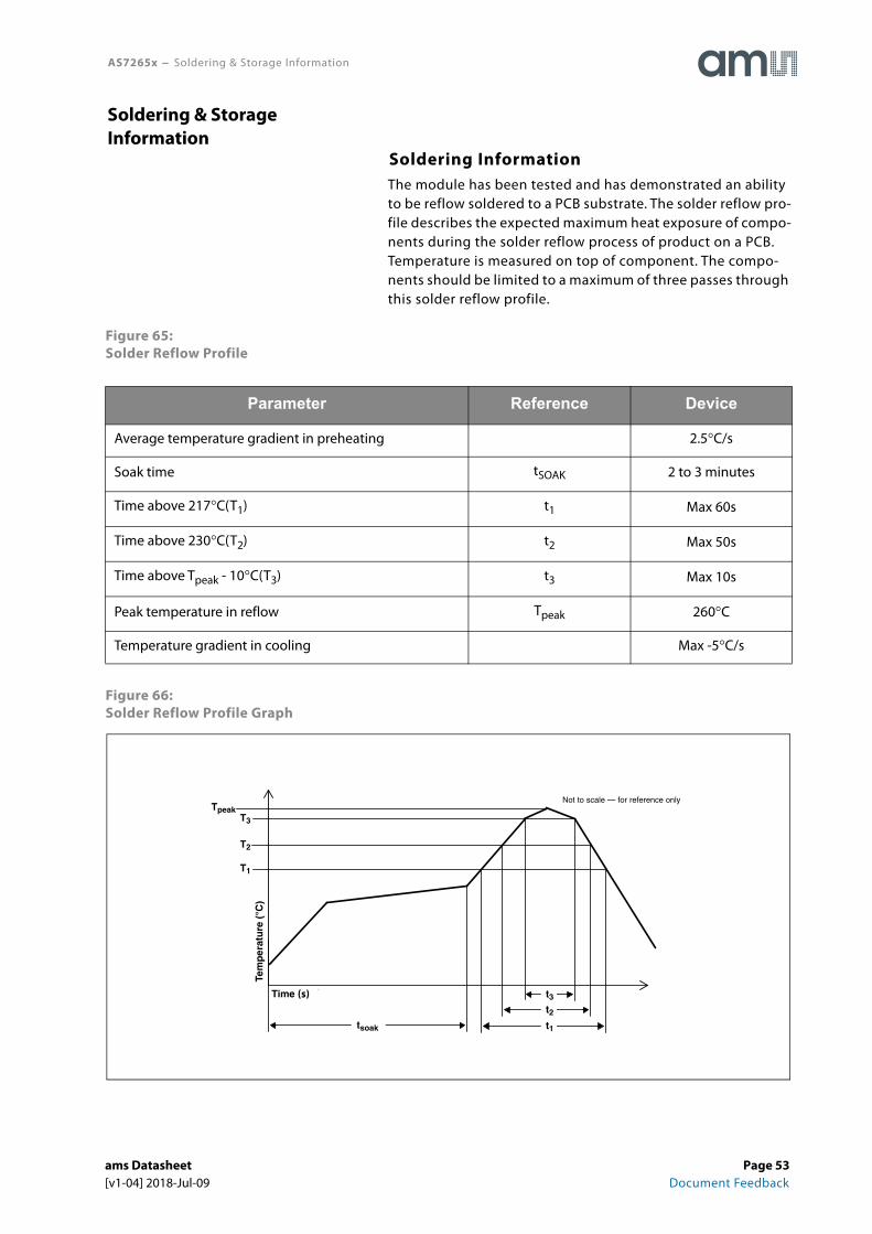
AS7265x − Soldering & Storage Information
Soldering InformationThe module has been tested and has demonstrated an ability to be reflow soldered to a PCB substrate. The solder reflow pro-file describes the expected maximum heat exposure of compo-nents during the solder reflow process of product on a PCB. Temperature is measured on top of component. The compo-nents should be limited to a maximum of three passes through this solder reflow profile.
Figure 65:Solder Reflow Profile
Figure 66:Solder Reflow Profile Graph
Parameter Reference Device
Average temperature gradient in preheating 2.5°C/s
Soak time tSOAK 2 to 3 minutes
Time above 217°C(T1) t1 Max 60s
Time above 230°C(T2) t2 Max 50s
Time above Tpeak - 10°C(T3) t3 Max 10s
Peak temperature in reflow Tpeak 260°C
Temperature gradient in cooling Max -5°C/s
Soldering & Storage Information
ams Datasheet Page 53[v1-04] 2018-Jul-09 Document Feedback

AS7265x − Soldering & Storage Information
Manufacturing Process ConsiderationsThe AS72651,AS72652 and AS72653 packages are compatible with standard reflow no-clean and cleaning processes including aqueous, solvent or ultrasonic techniques. However, as an open-aperture device, precautions must be taken to avoid particulate or solvent contamination as a result of any manufacturing processes, including pick and place, reflow, cleaning, integration assembly and/or testing. Temporary covering of the aperture is allowed. To avoid degradation of accuracy or performance in the end product, care should be taken that any temporary covering and associated sealants/debris are thoroughly removed prior to any optical testing or final packaging.
Storage Information
Moisture SensitivityOptical characteristics of the device can be adversely affected during the soldering process by the release and vaporization of moisture that has been previously absorbed into the package. To ensure the package contains the smallest amount of absorbed moisture possible, each device is baked prior to being dry packed for shipping.
Devices are dry packed in a sealed aluminized envelope called a moisture-barrier bag with silica gel to protect them from ambient moisture during shipping, handling, and storage before use.
Shelf Life
The calculated shelf life of the device in an unopened moisture barrier bag is 12 months from the date code on the bag when stored under the following conditions:
• Shelf Life: 12 months
• Ambient Temperature: <40°C
• Relative Humidity: <90%
Rebaking of the devices will be required if the devices exceed the 12 month shelf life or the Humidity Indicator Card shows that the devices were exposed to conditions beyond the allowable moisture region.
Page 54 ams Datasheet Document Feedback [v1-04] 2018-Jul-09

AS7265x − Soldering & Storage Information
Floor Life
The module has been assigned a moisture sensitivity level of MSL 3. As a result, the floor life of devices removed from the moisture barrier bag is 168 hours from the time the bag was opened, provided that the devices are stored under the following conditions:
Floor Life: 168 hours
Ambient Temperature: <30°C
Relative Humidity: <60%
If the floor life or the temperature/humidity conditions have been exceeded, the devices must be rebaked prior to solder reflow or dry packing.
Rebaking InstructionsWhen the shelf life or floor life limits have been exceeded, rebake at 50°C for 12 hours.
ams Datasheet Page 55[v1-04] 2018-Jul-09 Document Feedback
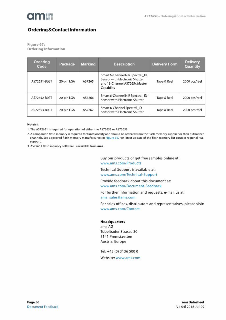
AS7265x − Ordering & Contact Information
Figure 67:Ordering Information
Note(s):
1. The AS72651 is required for operation of either the AS72652 or AS72653.
2. A companion flash memory is required for functionality and should be ordered from the flash memory supplier or their authorized channels. See approved flash memory manufacturers in Figure 56. For latest update of the flash memory list contact regional FAE support.
3. AS72651 flash memory software is available from ams.
Buy our products or get free samples online at:www.ams.com/Products
Technical Support is available at:www.ams.com/Technical-Support
Provide feedback about this document at:www.ams.com/Document-Feedback
For further information and requests, e-mail us at:[email protected]
For sales offices, distributors and representatives, please visit: www.ams.com/Contact
Headquartersams AGTobelbader Strasse 308141 PremstaettenAustria, Europe
Tel: +43 (0) 3136 500 0
Website: www.ams.com
Ordering Code Package Marking Description Delivery Form Delivery
Quantity
AS72651-BLGT 20-pin LGA AS7265
Smart 6-Channel NIR Spectral_ID Sensor with Electronic Shutter and 18-Channel AS7265x Master Capability
Tape & Reel 2000 pcs/reel
AS72652-BLGT 20-pin LGA AS7266Smart 6-Channel NIR Spectral_ID Sensor with Electronic Shutter
Tape & Reel 2000 pcs/reel
AS72653-BLGT 20-pin LGA AS7267Smart 6-Channel Spectral_ID Sensor with Electronic Shutter
Tape & Reel 2000 pcs/reel
Ordering & Contact Information
Page 56 ams Datasheet Document Feedback [v1-04] 2018-Jul-09

AS7265x − RoHS Compliant & ams Green Statement
RoHS: The term RoHS compliant means that ams AG products fully comply with current RoHS directives. Our semiconductor products do not contain any chemicals for all 6 substance categories, including the requirement that lead not exceed 0.1% by weight in homogeneous materials. Where designed to be soldered at high temperatures, RoHS compliant products are suitable for use in specified lead-free processes.
ams Green (RoHS compliant and no Sb/Br): ams Green defines that in addition to RoHS compliance, our products are free of Bromine (Br) and Antimony (Sb) based flame retardants (Br or Sb do not exceed 0.1% by weight in homogeneous material).
Important Information: The information provided in this statement represents ams AG knowledge and belief as of the date that it is provided. ams AG bases its knowledge and belief on information provided by third parties, and makes no representation or warranty as to the accuracy of such information. Efforts are underway to better integrate information from third parties. ams AG has taken and continues to take reasonable steps to provide representative and accurate information but may not have conducted destructive testing or chemical analysis on incoming materials and chemicals. ams AG and ams AG suppliers consider certain information to be proprietary, and thus CAS numbers and other limited information may not be available for release.
RoHS Compliant & ams Green Statement
ams Datasheet Page 57[v1-04] 2018-Jul-09 Document Feedback
AS7265x − Copyrights & Disclaimer
Copyright ams AG, Tobelbader Strasse 30, 8141 Premstaetten, Austria-Europe. Trademarks Registered. All rights reserved. The material herein may not be reproduced, adapted, merged, translated, stored, or used without the prior written consent of the copyright owner.
Devices sold by ams AG are covered by the warranty and patent indemnification provisions appearing in its General Terms of Trade. ams AG makes no warranty, express, statutory, implied, or by description regarding the information set forth herein. ams AG reserves the right to change specifications and prices at any time and without notice. Therefore, prior to designing this product into a system, it is necessary to check with ams AG for current information. This product is intended for use in commercial applications. Applications requiring extended temperature range, unusual environmental requirements, or high reliability applications, such as military, medical life-support or life-sustaining equipment are specifically not recommended without additional processing by ams AG for each application. This product is provided by ams AG “AS IS” and any express or implied warranties, including, but not limited to the implied warranties of merchantability and fitness for a particular purpose are disclaimed.
ams AG shall not be liable to recipient or any third party for any damages, including but not limited to personal injury, property damage, loss of profits, loss of use, interruption of business or indirect, special, incidental or consequential damages, of any kind, in connection with or arising out of the furnishing, performance or use of the technical data herein. No obligation or liability to recipient or any third party shall arise or flow out of ams AG rendering of technical or other services.
Copyrights & Disclaimer
Page 58 ams Datasheet Document Feedback [v1-04] 2018-Jul-09

AS7265x − Document Status
Document Status Product Status Definition
Product Preview Pre-Development
Information in this datasheet is based on product ideas in the planning phase of development. All specifications are design goals without any warranty and are subject to change without notice
Preliminary Datasheet Pre-Production
Information in this datasheet is based on products in the design, validation or qualification phase of development. The performance and parameters shown in this document are preliminary without any warranty and are subject to change without notice
Datasheet Production
Information in this datasheet is based on products in ramp-up to full production or full production which conform to specifications in accordance with the terms of ams AG standard warranty as given in the General Terms of Trade
Datasheet (discontinued) Discontinued
Information in this datasheet is based on products which conform to specifications in accordance with the terms of ams AG standard warranty as given in the General Terms of Trade, but these products have been superseded and should not be used for new designs
Document Status
ams Datasheet Page 59[v1-04] 2018-Jul-09 Document Feedback

AS7265x − Revision Information
Changes from 1-03 (2017-Oct-17) to current revision 1-04 (2018-Jul-09) Page
Updated text under General Description 1
Updated text under Key Benefits & Features 1
Updated Figure 2 (AS7265x Chip- Set Block Diagram) 3
Renamed Figure 3 to “Pin Diagram of AS72651,AS72652 and AS72653 (Top View)” 4
Updated Figure 4 (AS72651 pin description) 4
Added Figure 5 (AS72652 and AS72653 pin description) 5
Updated text under “Absolute Maximum Ratings”(replaced AS72651 with AS7265x)
7
Updated titles names in Figure 6,8 to AS7265x 7,10
Updated title name in Figure 7 and notes under it 8
Updated text under Optical Characteristics 13
Moved Figure “AS7265x LGA Average Field of View” under “Optical Characteristics” 13
Updated Figure 14 13
Updated Figure 16 14
Updated Figure 18 16
Updated Figure 19 18
Updated title name in figure 20 and notes under it 18
Updated text under AS7265x 18-Channel Spectral_ID Detector Overview 19
Updated text under AS7265x LED_IND Controls 22
Updated text under Interrupt Operation 22
Updated text under Required Flash Memory 23
Updated text under I²C Feature List 23
Updated I²C Virtual Register Byte Write 25
Updated I²C Virtual Register Byte Read 26
Updated Figure 26 28
Updated text under Detailed Register Descriptions including Figure 27 to 51 31
Updated text under UART Command Interface 41
Added Figure 56(List of ams approved flash manufacturer) 41
Updated text under Figure 58 43
Revision Information
Page 60 ams Datasheet Document Feedback [v1-04] 2018-Jul-09

AS7265x − Revision Information
Note(s):
1. Page and figure numbers for the previous version may differ from page and figure numbers in the current revision.
2. Correction of typographical errors is not explicitly mentioned.
Updated Figure 59 (AS7265x AT Commands) and text above it 43
Updated Figure 60 (Typical AS7265x 18-Channel Application Circuit) 48
Updated text under Manufacturing Process Considerations(replaced AS72651 with AS72651, AS72652,AS72653)
54
Updated note under Figure 67 56
Changes from 1-03 (2017-Oct-17) to current revision 1-04 (2018-Jul-09) Page
ams Datasheet Page 61[v1-04] 2018-Jul-09 Document Feedback

AS7265x − Content Guide
1 General Description1 Key Benefits & Features2 Applications3 Block Diagram
4 Pin Assignments7 Absolute Maximum Ratings
8 Electrical Characteristics10 Timing Characteristics
13 Typical Operating Characteristics13 Optical Characteristics
19 Detailed Description19 AS7265x 18-Channel Spectral_ID Detector
Overview19 Channel Data Conversion of the AS7265x
Devices21 RC Oscillator21 Temperature Sensor22 Reset22 AS7265x LED_IND Controls22 Electronic Shutter with AS7265x LED_DRV Driver Con-
trol22 Interrupt Operation23 Required Flash Memory23 I²C Slave Interface23 I²C Feature List24 I²C Virtual Register Write Access25 I²C Virtual Register Byte Write26 I²C Virtual Register Byte Read27 4-Byte Floating-Point (FP) Registers28 I²C Virtual Register Set31 Detailed Register Descriptions39 AS72651 I2C Firmware (FW) Update Procedure41 UART Command Interface41 UART Feature List41 Operation41 Transmission41 Reception42 AT Command Interface
48 Application Information49 Package Drawings & Markings50 PCB Pad Layout52 Mechanical Data
53 Soldering & Storage Information53 Soldering Information54 Manufacturing Process Considerations54 Storage Information54 Moisture Sensitivity55 Rebaking Instructions
Content Guide
Page 62 ams Datasheet Document Feedback [v1-04] 2018-Jul-09

AS7265x − Content Guide
56 Ordering & Contact Information57 RoHS Compliant & ams Green Statement58 Copyrights & Disclaimer59 Document Status60 Revision Information
ams Datasheet Page 63[v1-04] 2018-Jul-09 Document Feedback
![AS7265x - Mouser Electronics · 2019. 5. 6. · Page 2 ams Datasheet Document Feedback [v1-04] 2018-Jul-09 AS7265x − General Description Figure 1: AS7265x Chip-Set Benefits and](https://img.pdfslide.us/doc/110x75/60014646c89a48252f59f22d/as7265x-mouser-electronics-2019-5-6-page-2-ams-datasheet-document-feedback.jpg)