Embed Size (px)
Citation preview
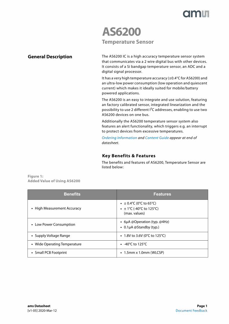
AS6200Temperature Sensor
The AS6200 IC is a high accuracy temperature sensor system that communicates via a 2 wire digital bus with other devices. It consists of a Si bandgap temperature sensor, an ADC and a digital signal processor.
It has a very high temperature accuracy (±0.4°C for AS6200) and an ultra-low power consumption (low operation and quiescent current) which makes it ideally suited for mobile/battery powered applications.
The AS6200 is an easy to integrate and use solution, featuring an factory calibrated sensor, integrated linearization and the possibility to use 2 different I²C addresses, enabling to use two AS6200 devices on one bus.
Additionally the AS6200 temperature sensor system also features an alert functionality, which triggers e.g. an interrupt to protect devices from excessive temperatures.
Ordering Information and Content Guide appear at end of datasheet.
Key Benefits & Features The benefits and features of AS6200, Temperature Sensor are listed below:
Figure 1:Added Value of Using AS6200
Benefits Features
• High Measurement Accuracy• ± 0.4°C (0°C to 65°C)• ± 1°C (-40°C to 125°C)
(max. values)
• Low Power Consumption• 6μA @Operation (typ. @4Hz)• 0.1μA @Standby (typ.)
• Supply Voltage Range • 1.8V to 3.6V (0°C to 125°C)
• Wide Operating Temperature • -40°C to 125°C
• Small PCB Footprint • 1.5mm x 1.0mm (WLCSP)
General Description
ams Datasheet Page 1[v1-05] 2020-Mar-12 Document Feedback
AS6200 − General Description
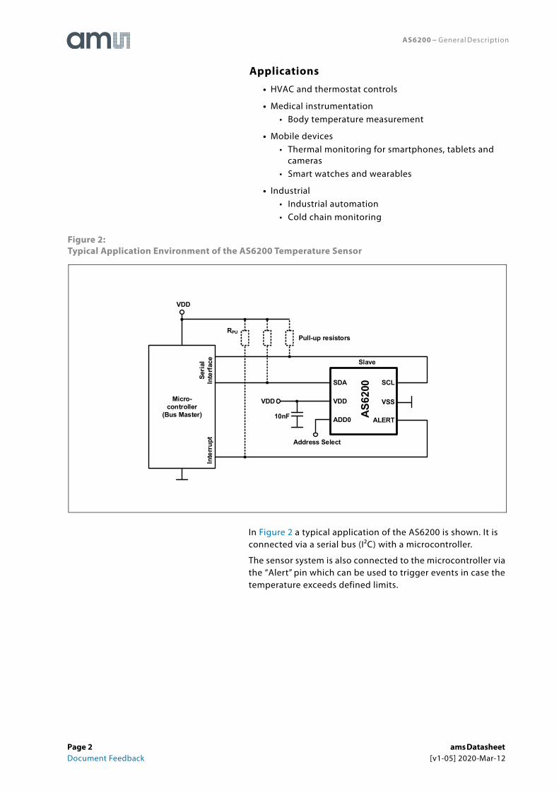
Applications
• HVAC and thermostat controls
• Medical instrumentation• Body temperature measurement
• Mobile devices• Thermal monitoring for smartphones, tablets and
cameras• Smart watches and wearables
• Industrial• Industrial automation• Cold chain monitoring
Figure 2:Typical Application Environment of the AS6200 Temperature Sensor
In Figure 2 a typical application of the AS6200 is shown. It is connected via a serial bus (I²C) with a microcontroller.
The sensor system is also connected to the microcontroller via the “Alert” pin which can be used to trigger events in case the temperature exceeds defined limits.
Micro-controller
(Bus Master)
VDD
10nF
VDD
Address Select
Slave
Seria
lIn
terfa
ceIn
terr
upt
Pull-up resistorsRPU
SDA
VDD
ADD0
SCL
ALERT
VSS
AS62
00
Page 2 ams Datasheet Document Feedback [v1-05] 2020-Mar-12
AS6200 − General Description
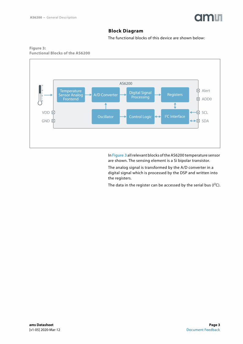
Block DiagramThe functional blocks of this device are shown below:
Figure 3:Functional Blocks of the AS6200
In Figure 3 all relevant blocks of the AS6200 temperature sensor are shown. The sensing element is a Si bipolar transistor.
The analog signal is transformed by the A/D converter in a digital signal which is processed by the DSP and written into the registers.
The data in the register can be accessed by the serial bus (I²C).
A/D Converter
AS6200
TemperatureSensor Analog
Frontend
Digital SignalProcessing
Oscillator Control Logic
Registers
I2C Interface
Alert
ADD0
SCL
SDA
VDD
GND
ams Datasheet Page 3[v1-05] 2020-Mar-12 Document Feedback
AS6200 − Pin Assignments
Figure 4:Pin Assignment WLCSP (Top View)
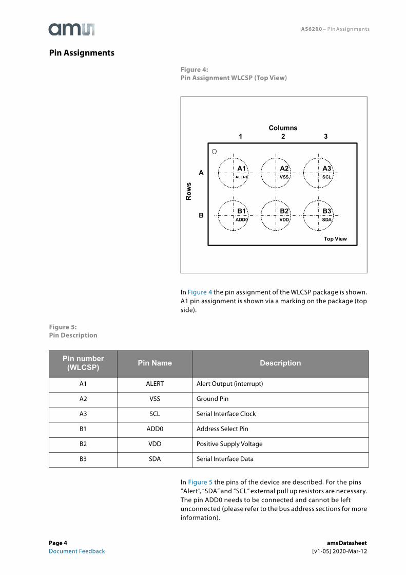
In Figure 4 the pin assignment of the WLCSP package is shown. A1 pin assignment is shown via a marking on the package (top side).
Figure 5:Pin Description
In Figure 5 the pins of the device are described. For the pins “Alert”, “SDA” and “SCL” external pull up resistors are necessary. The pin ADD0 needs to be connected and cannot be left unconnected (please refer to the bus address sections for more information).
Pin number (WLCSP) Pin Name Description
A1 ALERT Alert Output (interrupt)
A2 VSS Ground Pin
A3 SCL Serial Interface Clock
B1 ADD0 Address Select Pin
B2 VDD Positive Supply Voltage
B3 SDA Serial Interface Data
Pin Assignments
A
B
Row
s
1 2 3Columns
A3A2A1
B3B2B1
Top View
SCLVSSALERT
SDAVDDADD0
Page 4 ams Datasheet Document Feedback [v1-05] 2020-Mar-12

AS6200 − Absolute Maximum Ratings
Stresses beyond those listed under Absolute Maximum Ratings may cause permanent damage to the device. These are stress ratings only. Functional operation of the device at these or any other conditions beyond those indicated under Operating Conditions is not implied. Exposure to absolute maximum rating conditions for extended periods may affect device reliability.
Figure 6:Absolute Maximum Ratings
Symbol Parameter Min Max Units Comments
Electrical Parameters
VDD /VSSSupply Voltage to Ground
-0.3 4 V
ISCRInput Current (latch-up immunity)
-100 100 mA JEDEC JESD78D
Electrostatic Discharge
ESDHBMElectrostatic Discharge HBM
±2 kV MIL-STD-833J-3015.9
Temperature Ranges and Storage Conditions
TA Operating Temperature -40 125 °C
TJ Junction Temperature 125 °C
TSTRGStorage Temperature Range
-55 125 °C
TBODYPackage Body Temperature
260 °C
IPC/JEDEC J-STD-020The reflow peak soldering temperature (body temperature) is specified according to IPC/JEDEC J-STD-020 “Moisture/Reflow Sensitivity Classification for Non-hermetic Solid State Surface Mount Devices.”
RHNCRelative Humidity non-condensing
5 85 %
MSLMoisture Sensitivity Level
1 Maximum floor life time is unlimited
Absolute Maximum Ratings
ams Datasheet Page 5[v1-05] 2020-Mar-12 Document Feedback
AS6200 − Electrical Characteristics
Operating Conditions
Figure 7:Operating Conditions
Analog System Parameters
Figure 8:Analog System Parameters
Note(s):
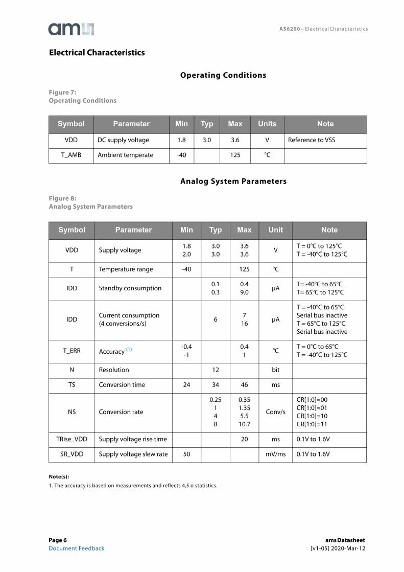
1. The accuracy is based on measurements and reflects 4,5 σ statistics.
Symbol Parameter Min Typ Max Units Note
VDD DC supply voltage 1.8 3.0 3.6 V Reference to VSS
T_AMB Ambient temperate -40 125 °C
Symbol Parameter Min Typ Max Unit Note
VDD Supply voltage1.82.0
3.03.0
3.63.6
VT = 0°C to 125°CT = -40°C to 125°C
T Temperature range -40 125 °C
IDD Standby consumption0.10.3
0.49.0
μAT= -40°C to 65°CT= 65°C to 125°C
IDDCurrent consumption(4 conversions/s)
67
16μA
T = -40°C to 65°C Serial bus inactiveT = 65°C to 125°CSerial bus inactive
T_ERR Accuracy (1) -0.4-1
0.41
°CT = 0°C to 65°CT = -40°C to 125°C
N Resolution 12 bit
TS Conversion time 24 34 46 ms
NS Conversion rate
0.25148
0.351.355.5
10.7
Conv/s
CR[1:0]=00CR[1:0]=01CR[1:0]=10CR[1:0]=11
TRise_VDD Supply voltage rise time 20 ms 0.1V to 1.6V
SR_VDD Supply voltage slew rate 50 mV/ms 0.1V to 1.6V
Electrical Characteristics
Page 6 ams Datasheet Document Feedback [v1-05] 2020-Mar-12
AS6200 − Detailed Descriptions
The AS6200 is a complete sensor system that has an integrated temperature sensing element, the analog frontend, the A/D converter and the digital signal processing part.
The digital signal processing part consists of the signal processor, the registers and the serial bus interface.
For block diagram please refer to Figure 3.
In Figure 8 an overview of the analog system parameters is given.
The current consumption with fewer conversions per second is lower than the values mentioned in Figure 8.
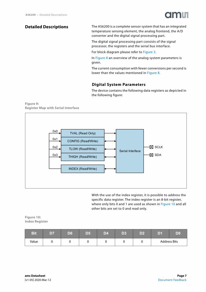
Digital System Parameters The device contains the following data registers as depicted in the following figure:
Figure 9:Register Map with Serial Interface
With the use of the index register, it is possible to address the specific data register. The index register is an 8-bit register, where only bits 0 and 1 are used as shown in Figure 10 and all other bits are set to 0 and read only.
Figure 10:Index Register
Bit D7 D6 D5 D4 D3 D2 D1 D0
Value 0 0 0 0 0 0 Address Bits
Detailed Descriptions
TVAL (Read Only)
CONFIG (Read/Write)
TLOW (Read/Write)
THIGH (Read/Write)
INDEX (Read/Write)
Serial Interface
0x0
0x1
0x2
0x3
SCLK
SDA
ams Datasheet Page 7[v1-05] 2020-Mar-12 Document Feedback

AS6200 − Detailed Descriptions
The two-bit address selects the register to be accessed by the serial interface as shown in the following table.
Figure 11:Register Map
This means that in order to access the different registers, the index register must be set accordingly. With the exception of the TVAL register (which contains the temperature value data), all registers are read/write accessible.
Configuration RegisterThe configuration register is a 16-bit register which defines the operation modes of the device. Any read/write operations processes the MSB byte first.
Figure 12:Configuration Register
In Figure 12 the configuration register is shown. The bits D0-3 and D13-14 are not to be used and are set to read only. The bit D4 is RW and must not be changed from the default value. The explanation of the other bits are detailed in the following sections.
Alert, Bit D5
The alert bit can be used to easily compare the current temperature reading to the thresholds that can be set in the TLOW and THIGH registers.
If the polarity bit is set to 0, the AL bit is read as 1 until the converted temperature value exceeds the defined value in the high temperature threshold register THIGH for the number of defined consecutive faults (bits CF). Such an event causes the
Address Symbol Register Description
0x0 TVAL Temperature Register Contains the temperature value
0x1 CONFIG Configuration Register Configuration settings of the temperature sensor
0x2 TLOW TLOW Register Low temperature threshold value
0x3 THIGH THIGH Register High temperature threshold value
Bit D15 D14 D13 D12 D11 D10 D9 D8 D7 D6 D5 D4 D3 D2 D1 D0
R/W RW RO RW RO RW RO
Bit SS Reserved CF POL IM SM CR AL Reserved
Default 0 1 0 0 0 0 0 0 1 0 1 0 0 0 0 0
MSB Byte LSB Byte
Page 8 ams Datasheet Document Feedback [v1-05] 2020-Mar-12
AS6200 − Detailed Descriptions
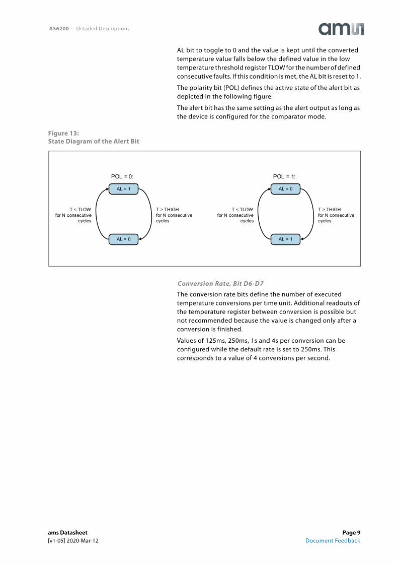
AL bit to toggle to 0 and the value is kept until the converted temperature value falls below the defined value in the low temperature threshold register TLOW for the number of defined consecutive faults. If this condition is met, the AL bit is reset to 1.
The polarity bit (POL) defines the active state of the alert bit as depicted in the following figure.
The alert bit has the same setting as the alert output as long as the device is configured for the comparator mode.
Figure 13:State Diagram of the Alert Bit
Conversion Rate, Bit D6-D7
The conversion rate bits define the number of executed temperature conversions per time unit. Additional readouts of the temperature register between conversion is possible but not recommended because the value is changed only after a conversion is finished.
Values of 125ms, 250ms, 1s and 4s per conversion can be configured while the default rate is set to 250ms. This corresponds to a value of 4 conversions per second.
AL = 1
AL = 0
T > THIGHfor N consecutivecycles
T < TLOWfor N consecutive
cycles
POL = 0:
AL = 0
AL = 1
T > THIGHfor N consecutivecycles
T < TLOWfor N consecutive
cycles
POL = 1:
ams Datasheet Page 9[v1-05] 2020-Mar-12 Document Feedback
AS6200 − Detailed Descriptions
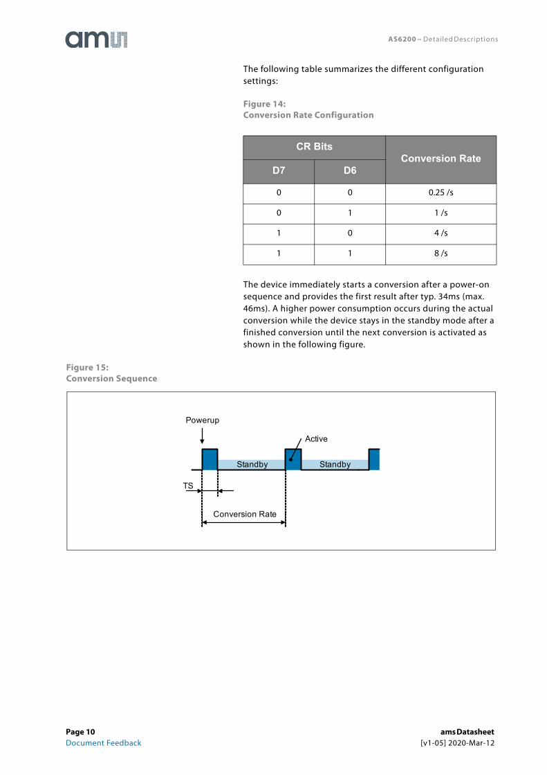
The following table summarizes the different configuration settings:
Figure 14:Conversion Rate Configuration
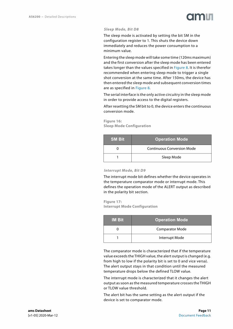
The device immediately starts a conversion after a power-on sequence and provides the first result after typ. 34ms (max. 46ms). A higher power consumption occurs during the actual conversion while the device stays in the standby mode after a finished conversion until the next conversion is activated as shown in the following figure.
Figure 15:Conversion Sequence
CR BitsConversion Rate
D7 D6
0 0 0.25 /s
0 1 1 /s
1 0 4 /s
1 1 8 /s
Powerup
TS
Conversion Rate
Active
Standby Standby
Page 10 ams Datasheet Document Feedback [v1-05] 2020-Mar-12
AS6200 − Detailed Descriptions
Sleep Mode, Bit D8
The sleep mode is activated by setting the bit SM in the configuration register to 1. This shuts the device down immediately and reduces the power consumption to a minimum value.
Entering the sleep mode will take some time (120ms maximum) and the first conversion after the sleep mode has been entered takes longer than the values specified in Figure 8. It is therefor recommended when entering sleep mode to trigger a single shot conversion at the same time. After 150ms, the device has then entered the sleep mode and subsequent conversion times are as specified in Figure 8.
The serial interface is the only active circuitry in the sleep mode in order to provide access to the digital registers.
After resetting the SM bit to 0, the device enters the continuous conversion mode.
Figure 16:Sleep Mode Configuration
Interrupt Mode, Bit D9
The interrupt mode bit defines whether the device operates in the temperature comparator mode or interrupt mode. This defines the operation mode of the ALERT output as described in the polarity bit section.
Figure 17:Interrupt Mode Configuration
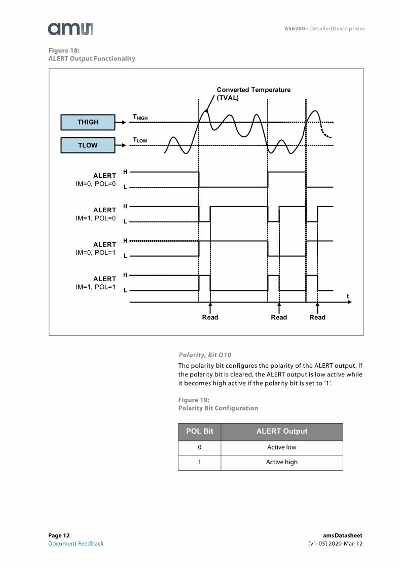
The comparator mode is characterized that if the temperature value exceeds the THIGH value, the alert output is changed (e.g. from high to low if the polarity bit is set to 0 and vice versa). The alert output stays in that condition until the measured temperature drops below the defined TLOW value.
The interrupt mode is characterized that it changes the alert output as soon as the measured temperature crosses the THIGH or TLOW value threshold.
The alert bit has the same setting as the alert output if the device is set to comparator mode.
SM Bit Operation Mode
0 Continuous Conversion Mode
1 Sleep Mode
IM Bit Operation Mode
0 Comparator Mode
1 Interrupt Mode
ams Datasheet Page 11[v1-05] 2020-Mar-12 Document Feedback
AS6200 − Detailed Descriptions
Figure 18:ALERT Output Functionality
Polarity, Bit D10
The polarity bit configures the polarity of the ALERT output. If the polarity bit is cleared, the ALERT output is low active while it becomes high active if the polarity bit is set to ‘1’.
Figure 19:Polarity Bit Configuration
POL Bit ALERT Output
0 Active low
1 Active high
THIGH
TLOW
Converted Temperature(TVAL)
THIGH
TLOW
t
Read Read Read
ALERTIM=0, POL=0
ALERTIM=1, POL=0
H
L
H
L
H
L
H
L
ALERTIM=0, POL=1
ALERTIM=1, POL=1
Page 12 ams Datasheet Document Feedback [v1-05] 2020-Mar-12
AS6200 − Detailed Descriptions
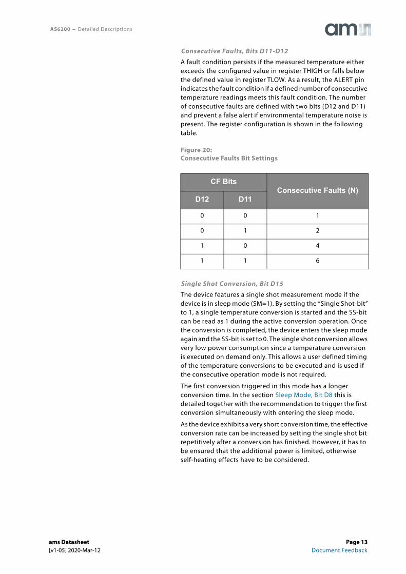
Consecutive Faults, Bits D11-D12
A fault condition persists if the measured temperature either exceeds the configured value in register THIGH or falls below the defined value in register TLOW. As a result, the ALERT pin indicates the fault condition if a defined number of consecutive temperature readings meets this fault condition. The number of consecutive faults are defined with two bits (D12 and D11) and prevent a false alert if environmental temperature noise is present. The register configuration is shown in the following table.
Figure 20:Consecutive Faults Bit Settings
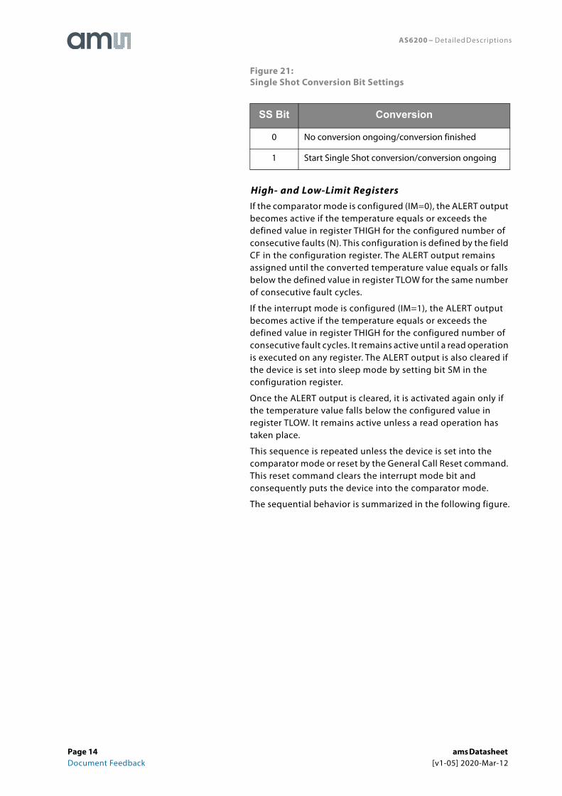
Single Shot Conversion, Bit D15
The device features a single shot measurement mode if the device is in sleep mode (SM=1). By setting the “Single Shot-bit” to 1, a single temperature conversion is started and the SS-bit can be read as 1 during the active conversion operation. Once the conversion is completed, the device enters the sleep mode again and the SS-bit is set to 0. The single shot conversion allows very low power consumption since a temperature conversion is executed on demand only. This allows a user defined timing of the temperature conversions to be executed and is used if the consecutive operation mode is not required.
The first conversion triggered in this mode has a longer conversion time. In the section Sleep Mode, Bit D8 this is detailed together with the recommendation to trigger the first conversion simultaneously with entering the sleep mode.
As the device exhibits a very short conversion time, the effective conversion rate can be increased by setting the single shot bit repetitively after a conversion has finished. However, it has to be ensured that the additional power is limited, otherwise self-heating effects have to be considered.
CF BitsConsecutive Faults (N)
D12 D11
0 0 1
0 1 2
1 0 4
1 1 6
ams Datasheet Page 13[v1-05] 2020-Mar-12 Document Feedback
AS6200 − Detailed Descriptions
Figure 21:Single Shot Conversion Bit Settings
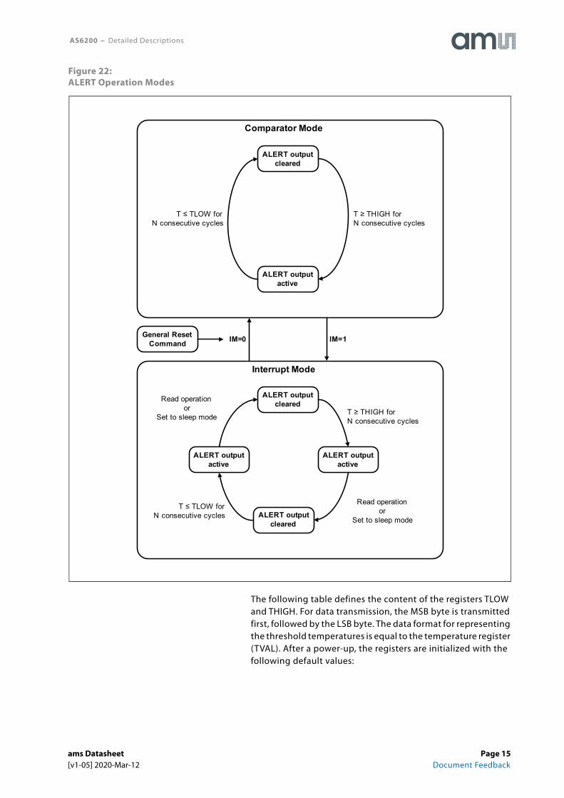
High- and Low-Limit RegistersIf the comparator mode is configured (IM=0), the ALERT output becomes active if the temperature equals or exceeds the defined value in register THIGH for the configured number of consecutive faults (N). This configuration is defined by the field CF in the configuration register. The ALERT output remains assigned until the converted temperature value equals or falls below the defined value in register TLOW for the same number of consecutive fault cycles.
If the interrupt mode is configured (IM=1), the ALERT output becomes active if the temperature equals or exceeds the defined value in register THIGH for the configured number of consecutive fault cycles. It remains active until a read operation is executed on any register. The ALERT output is also cleared if the device is set into sleep mode by setting bit SM in the configuration register.
Once the ALERT output is cleared, it is activated again only if the temperature value falls below the configured value in register TLOW. It remains active unless a read operation has taken place.
This sequence is repeated unless the device is set into the comparator mode or reset by the General Call Reset command. This reset command clears the interrupt mode bit and consequently puts the device into the comparator mode.
The sequential behavior is summarized in the following figure.
SS Bit Conversion
0 No conversion ongoing/conversion finished
1 Start Single Shot conversion/conversion ongoing
Page 14 ams Datasheet Document Feedback [v1-05] 2020-Mar-12
AS6200 − Detailed Descriptions
Figure 22:ALERT Operation Modes
The following table defines the content of the registers TLOW and THIGH. For data transmission, the MSB byte is transmitted first, followed by the LSB byte. The data format for representing the threshold temperatures is equal to the temperature register (TVAL). After a power-up, the registers are initialized with the following default values:
ALERT output cleared
ALERT output active
ALERT output cleared
ALERT output active
T ≥ THIGH for N consecutive cycles
Read operation or
Set to sleep mode
T ≤ TLOW for N consecutive cycles
Read operation or
Set to sleep mode
Interrupt Mode
ALERT output cleared
ALERT output active
Comparator Mode
T ≥ THIGH for N consecutive cycles
T ≤ TLOW for N consecutive cycles
IM=1IM=0General Reset Command
ams Datasheet Page 15[v1-05] 2020-Mar-12 Document Feedback
AS6200 − Detailed Descriptions
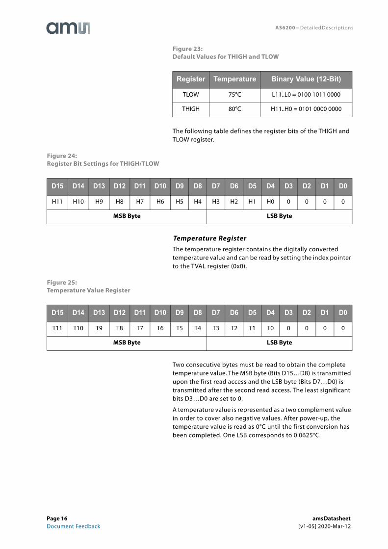
Figure 23:Default Values for THIGH and TLOW
The following table defines the register bits of the THIGH and TLOW register.
Figure 24:Register Bit Settings for THIGH/TLOW
Temperature RegisterThe temperature register contains the digitally converted temperature value and can be read by setting the index pointer to the TVAL register (0x0).
Figure 25:Temperature Value Register
Two consecutive bytes must be read to obtain the complete temperature value. The MSB byte (Bits D15…D8) is transmitted upon the first read access and the LSB byte (Bits D7…D0) is transmitted after the second read access. The least significant bits D3…D0 are set to 0.
A temperature value is represented as a two complement value in order to cover also negative values. After power-up, the temperature value is read as 0°C until the first conversion has been completed. One LSB corresponds to 0.0625°C.
Register Temperature Binary Value (12-Bit)
TLOW 75°C L11..L0 = 0100 1011 0000
THIGH 80°C H11..H0 = 0101 0000 0000
D15 D14 D13 D12 D11 D10 D9 D8 D7 D6 D5 D4 D3 D2 D1 D0
H11 H10 H9 H8 H7 H6 H5 H4 H3 H2 H1 H0 0 0 0 0
MSB Byte LSB Byte
D15 D14 D13 D12 D11 D10 D9 D8 D7 D6 D5 D4 D3 D2 D1 D0
T11 T10 T9 T8 T7 T6 T5 T4 T3 T2 T1 T0 0 0 0 0
MSB Byte LSB Byte
Page 16 ams Datasheet Document Feedback [v1-05] 2020-Mar-12
AS6200 − Detailed Descriptions
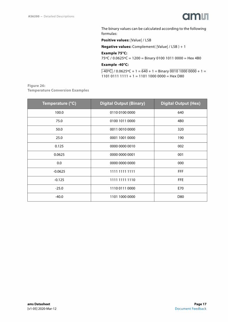
The binary values can be calculated according to the following formulas:
Positive values: |Value| / LSB
Negative values: Complement( |Value| / LSB ) + 1
Example 75°C: 75ºC / 0.0625ºC = 1200 = Binary 0100 1011 0000 = Hex 4B0
Example -40°C:
|-40ºC| / 0.0625ºC + 1 = 640 + 1 = Binary 0010 1000 0000 + 1 = 1101 0111 1111 + 1 = 1101 1000 0000 = Hex D80
Figure 26:Temperature Conversion Examples
Temperature (°C) Digital Output (Binary) Digital Output (Hex)
100.0 0110 0100 0000 640
75.0 0100 1011 0000 4B0
50.0 0011 0010 0000 320
25.0 0001 1001 0000 190
0.125 0000 0000 0010 002
0.0625 0000 0000 0001 001
0.0 0000 0000 0000 000
-0.0625 1111 1111 1111 FFF
-0.125 1111 1111 1110 FFE
-25.0 1110 0111 0000 E70
-40.0 1101 1000 0000 D80
ams Datasheet Page 17[v1-05] 2020-Mar-12 Document Feedback
AS6200 − Detailed Descriptions
Serial InterfaceThe device employs a standard I²C-Interface.
Bus DescriptionA data transfer must be invoked by a master device (e.g. microcontroller) which defines the access to the slave device. The master device defines and generates the serial clock (SCL) and the start/stop conditions.
In order to address a specific device, a START condition has to be generated by the master device by pulling the data line (SDA) from a logic high level to a logic low level while the serial clock signal (SCL) is kept at high level.
After the start condition, the slave address byte is transmitted which is completed with a ninth bit which indicates a read (bit=’1’) or a write operation (bit=’0’) respectively. All slaves read the data on the rising edge of the clock. An acknowledge signal is generated by the addressed slave during the ninth clock pulse. This acknowledge signal is produced by pulling the pin SDA to a low level by the selected slave.
Subsequently, the byte data transfer is started and finished by an acknowledge bit. A change in the data signal (SDA) while the clock signal (SCL) is high causes a START or STOP condition. Hence, it must be ensured such a condition is prevented during a data transfer phase.
After completing the data transfer, the master generates a STOP condition by pulling the data line (SDA) from low level to high level while the clock signal (SCL) is kept at high level.
Data InterfaceA bus connection is created by connecting the open drain input/output lines SDA and SCL to the two wire bus. The inputs of SDA and SCL feature Schmitt-trigger inputs as well as low pass filters in order to suppress noise on the bus line. This improves the robustness against spikes on the two wire interface.
Both fast transmission mode (1kHz to 400kHz) and high-speed transmission mode (1kHz to 3.4MHz) are employed to cover different bus speed settings.
Any data transfer transmits the MSB first and the LSB as last bit.
Page 18 ams Datasheet Document Feedback [v1-05] 2020-Mar-12
AS6200 − Detailed Descriptions
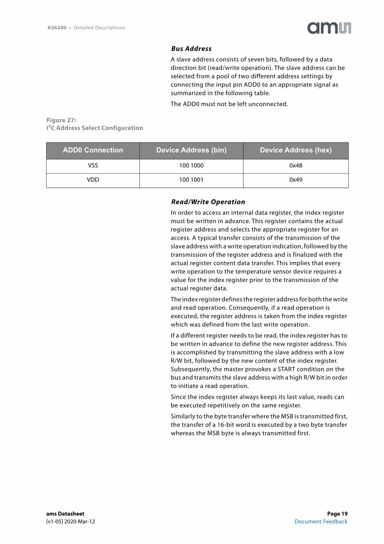
Bus AddressA slave address consists of seven bits, followed by a data direction bit (read/write operation). The slave address can be selected from a pool of two different address settings by connecting the input pin ADD0 to an appropriate signal as summarized in the following table.
The ADD0 must not be left unconnected.
Figure 27:I²C Address Select Configuration
Read/Write OperationIn order to access an internal data register, the index register must be written in advance. This register contains the actual register address and selects the appropriate register for an access. A typical transfer consists of the transmission of the slave address with a write operation indication, followed by the transmission of the register address and is finalized with the actual register content data transfer. This implies that every write operation to the temperature sensor device requires a value for the index register prior to the transmission of the actual register data.
The index register defines the register address for both the write and read operation. Consequently, if a read operation is executed, the register address is taken from the index register which was defined from the last write operation.
If a different register needs to be read, the index register has to be written in advance to define the new register address. This is accomplished by transmitting the slave address with a low R/W bit, followed by the new content of the index register. Subsequently, the master provokes a START condition on the bus and transmits the slave address with a high R/W bit in order to initiate a read operation.
Since the index register always keeps its last value, reads can be executed repetitively on the same register.
Similarly to the byte transfer where the MSB is transmitted first, the transfer of a 16-bit word is executed by a two byte transfer whereas the MSB byte is always transmitted first.
ADD0 Connection Device Address (bin) Device Address (hex)
VSS 100 1000 0x48
VDD 100 1001 0x49
ams Datasheet Page 19[v1-05] 2020-Mar-12 Document Feedback
AS6200 − Detailed Descriptions
Slave OperationThe device employs a slave functionality only (slave transmitter and slave receiver) and cannot be operated as a bus master. Consequently, the device never actively drives the SCL line.
Slave Receiver Mode
Any transmission is invoked by the master device by transmitting the slave address with a low R/W bit. Subsequently, the slave device acknowledges the reception of the valid address by pulling the ninth bit to a low level. Following to acknowledge, the master transmits the content of the index register. This transfer is again acknowledged by the slave device. The next data byte(s) are written to the actual data register which is selected by the index register while each transfer is acknowledged upon a completed transfer by the slave device. A data transfer can be finished if the master transmits a START or a STOP condition on the bus.
Slave Transmitter Mode
The master transmits the slave address with a high R/W bit. In turn, the slave acknowledges a valid slave address. Subsequently, the slave transmits the MSB byte of the actual selected data register by the index register. After the MSB byte transmission, acknowledge is sent by the master. Afterwards, the LSB byte is transmitted by the slave which is also acknowledged by the master after the completed transmission. The data transfer can be terminated by the master by transmitting a Not-Acknowledge after the transmitted slave data or by invoking a START or a STOP condition on the bus.
Alert Function
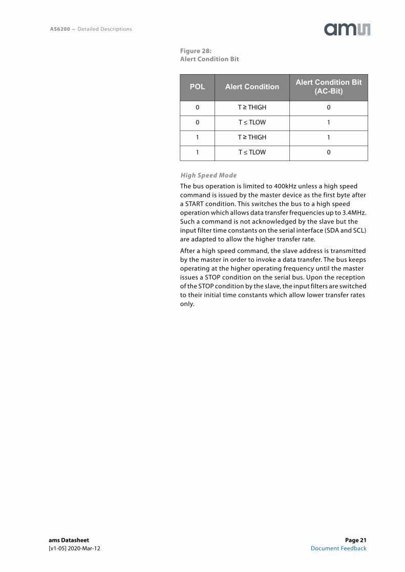
If the device is configured for an interrupt mode operation (IM=1), the ALERT output can be used as an alert signal.
If the polarity bit is set to ‘0’ (POL=’0’), the alert condition bit is set to ‘0’ in case the temperature has exceeded the configured value in register THIGH. Accordingly, the alert condition bit is set to ‘1’ if the temperature has fallen below the configured value in register TLOW.
If the polarity bit is set to ‘1’ (POL=’1’), the alert condition bit is inverted. The following table summarizes the status of the alert condition bit with different alert conditions and polarity configurations.
Page 20 ams Datasheet Document Feedback [v1-05] 2020-Mar-12
AS6200 − Detailed Descriptions
Figure 28:Alert Condition Bit
High Speed Mode
The bus operation is limited to 400kHz unless a high speed command is issued by the master device as the first byte after a START condition. This switches the bus to a high speed operation which allows data transfer frequencies up to 3.4MHz. Such a command is not acknowledged by the slave but the input filter time constants on the serial interface (SDA and SCL) are adapted to allow the higher transfer rate.
After a high speed command, the slave address is transmitted by the master in order to invoke a data transfer. The bus keeps operating at the higher operating frequency until the master issues a STOP condition on the serial bus. Upon the reception of the STOP condition by the slave, the input filters are switched to their initial time constants which allow lower transfer rates only.
POL Alert Condition Alert Condition Bit (AC-Bit)
0 T ≥ THIGH 0
0 T ≤ TLOW 1
1 T ≥ THIGH 1
1 T ≤ TLOW 0
ams Datasheet Page 21[v1-05] 2020-Mar-12 Document Feedback
AS6200 − Detailed Descriptions
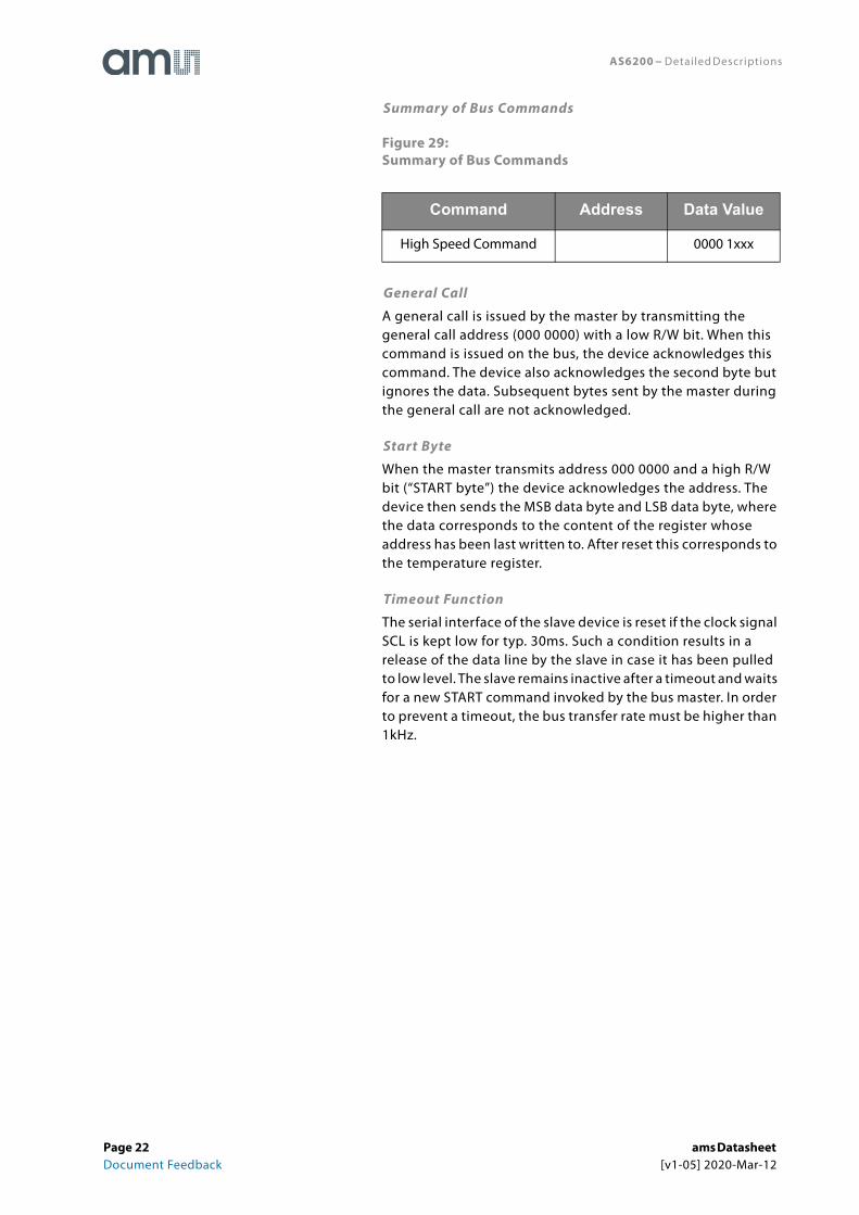
Summary of Bus Commands
Figure 29:Summary of Bus Commands
General Call
A general call is issued by the master by transmitting the general call address (000 0000) with a low R/W bit. When this command is issued on the bus, the device acknowledges this command. The device also acknowledges the second byte but ignores the data. Subsequent bytes sent by the master during the general call are not acknowledged.
Start Byte
When the master transmits address 000 0000 and a high R/W bit (“START byte”) the device acknowledges the address. The device then sends the MSB data byte and LSB data byte, where the data corresponds to the content of the register whose address has been last written to. After reset this corresponds to the temperature register.
Timeout Function
The serial interface of the slave device is reset if the clock signal SCL is kept low for typ. 30ms. Such a condition results in a release of the data line by the slave in case it has been pulled to low level. The slave remains inactive after a timeout and waits for a new START command invoked by the bus master. In order to prevent a timeout, the bus transfer rate must be higher than 1kHz.
Command Address Data Value
High Speed Command 0000 1xxx
Page 22 ams Datasheet Document Feedback [v1-05] 2020-Mar-12
AS6200 − Detailed Descriptions
Bus Conditions
The following conditions occur on the serial bus which is compatible to the I²C-Bus.
• Bus Idle: The signals SDA and SCL are not actively driven and pulled to a high level by an external pull-up resistor.
• Start Data Transfer: A transition of the SDA input from high to low level while the SCL signal is kept at high level results in a START condition. Such a START condition must precede any data transfer.
• Stop Data Transfer: A transition of the SDA input from low to high level while the SCL signal is kept at high level results in a STOP condition. Any data transfer is finished by generating a STOP or START condition.
• Data Transfer: The master device defines the number of data bytes between a START and STOP condition and there is no limitation in the amount of data to be transmitted. If it is desired to read only a single MSB byte without the LSB byte, a termination of the data transfer can be provoked by issuing a START or STOP condition on the bus.
• Acknowledge: It is mandatory for each slave device to respond with acknowledge if the device is addressed by the master. Acknowledge is indicated by pulling down the data line (SDA) while the clock signal (SCL) is high in the acknowledge clock phase. In order to avoid an unwanted START or STOP condition on the bus, setup and hold times must be met. The master can signal an end of data transmission by transmitting a Not-Acknowledge on the last transmitted data byte by keeping the acknowledge bit at high level.
ams Datasheet Page 23[v1-05] 2020-Mar-12 Document Feedback
AS6200 − Detailed Descriptions
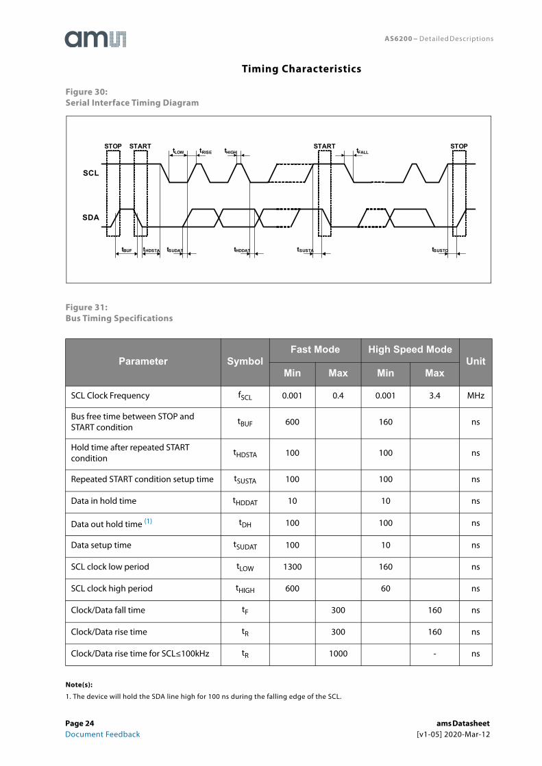
Timing Characteristics
Figure 30:Serial Interface Timing Diagram
Figure 31:Bus Timing Specifications
Note(s):
1. The device will hold the SDA line high for 100 ns during the falling edge of the SCL.
Parameter SymbolFast Mode High Speed Mode
UnitMin Max Min Max
SCL Clock Frequency fSCL 0.001 0.4 0.001 3.4 MHz
Bus free time between STOP and START condition
tBUF 600 160 ns
Hold time after repeated START condition
tHDSTA 100 100 ns
Repeated START condition setup time tSUSTA 100 100 ns
Data in hold time tHDDAT 10 10 ns
Data out hold time (1) tDH 100 100 ns
Data setup time tSUDAT 100 10 ns
SCL clock low period tLOW 1300 160 ns
SCL clock high period tHIGH 600 60 ns
Clock/Data fall time tF 300 160 ns
Clock/Data rise time tR 300 160 ns
Clock/Data rise time for SCL≤100kHz tR 1000 - ns
SCL
SDA
STOP START START STOP
tBUF tHDSTA
tLOW tRISE tHIGH tFALL
tSUSTAtSUDAT tHDDAT tSUSTO
Page 24 ams Datasheet Document Feedback [v1-05] 2020-Mar-12
AS6200 − Detailed Descriptions
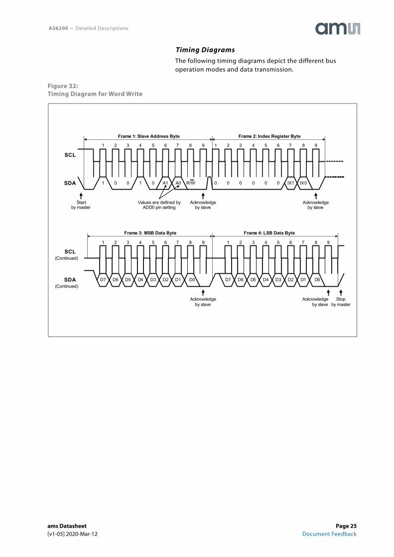
Timing DiagramsThe following timing diagrams depict the different bus operation modes and data transmission.
Figure 32:Timing Diagram for Word Write
1 2 3 4 5 6 7 8 9 1 2 3 4 5 6 7 8 9
SCL
SDA 1 0 0 1 0 A1 A0 R/W 0 0 0 0 0 0 IX1 IX0
Startby master
Values are defined by ADD0 pin setting
Frame 1: Slave Address Byte Frame 2: Index Register Byte
1 2 3 4 5 6 7 8 9 1 2 3 4 5 6 7 8 9
SCL
SDA
Frame 3: MSB Data Byte Frame 4: LSB Data Byte
D7 D6 D5 D4 D3 D2 D1 D0 D6 D5 D4 D3 D2 D1D7 D0
(Continued)
(Continued)
Acknowledgeby slave
Acknowledgeby slave
Acknowledgeby slave
Acknowledgeby slave
Stopby master
ams Datasheet Page 25[v1-05] 2020-Mar-12 Document Feedback
AS6200 − Detailed Descriptions
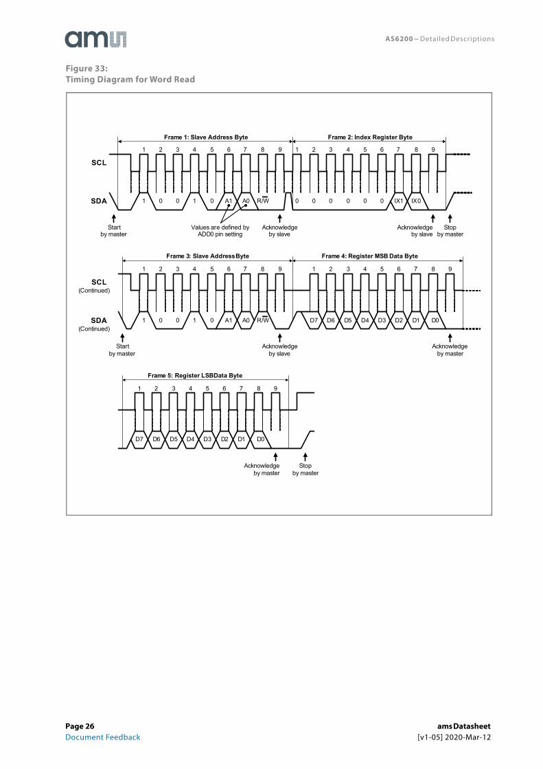
Figure 33:Timing Diagram for Word Read
1 2 3 4 5 6 7 8 9 1 2 3 4 5 6 7 8 9
SCL
SDA 1 0 0 1 0 A1 A0 R/W 0 0 0 0 0 0 IX1 IX0
Startby master
Values are defined by ADD0 pin setting
Frame 1: Slave Address Byte Frame 2: Index Register Byte
1 2 3 4 5 6 7 8 9 1 2 3 4 5 6 7 8 9
SCL
SDA
Frame 3: Slave AddressByte Frame 4: Register MSB Data Byte
D6 D5 D4 D3 D2 D1D7 D0
(Continued)
(Continued)
Acknowledgeby slave
Acknowledgeby slave
Acknowledgeby slave
Stopby master
1 0 0 1 0 A1 R/WA0
Startby master
Acknowledgeby master
1 2 3 4 5 6 7 8 9
Frame 5: Register LSBData Byte
D6 D5 D4 D3 D2 D1D7 D0
Acknowledgeby master
Stopby master
Page 26 ams Datasheet Document Feedback [v1-05] 2020-Mar-12
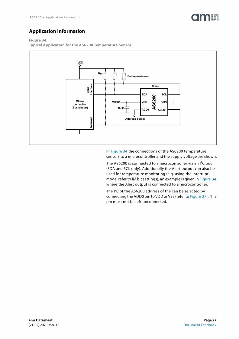
AS6200 − Application Information
Figure 34:Typical Application for the AS6200 Temperature Sensor
In Figure 34 the connections of the AS6200 temperature sensors to a microcontroller and the supply voltage are shown.
The AS6200 is connected to a microcontroller via an I²C bus (SDA and SCL only). Additionally the Alert output can also be used for temperature monitoring (e.g. using the interrupt mode, refer to IM bit settings), an example is given in Figure 34 where the Alert output is connected to a microcontroller.
The I²C of the AS6200 address of the can be selected by connecting the ADD0 pin to VDD or VSS (refer to Figure 27). This pin must not be left unconnected.
Application Information
Micro-controller
(Bus Master)
VDD
10nF
VDD
Address Select
SlaveSe
rial
Inte
rface
Inte
rrup
t
Pull-up resistorsRPU
SDA
VDD
ADD0
SCL
ALERT
VSS
AS62
00
ams Datasheet Page 27[v1-05] 2020-Mar-12 Document Feedback

AS6200 − Application Information
External Components
Figure 35:Schematic with External Components
Figure 36:Values for External Components
In Figure 35 and Figure 36 the schematics for external components are shown.
The decoupling capacitor for the supply should have a value of at least 10 nF.
The pull-up resistors on the serial interface and the interrupt also depend on the bus capacitance and on the clock speed, in Figure 36 recommended values are given.
Parameter Min Max Unit
Decoupling capacitor 10 nF
Pull-up resistors 10 18 kΩ
VDD
Decoupling Cap
VDD
Slave
Pull-up resistorsRPU
SDA
VDD
ADD0
SCL
ALERT
VSS
AS62
00
SCL
ALERT
SDA
Page 28 ams Datasheet Document Feedback [v1-05] 2020-Mar-12
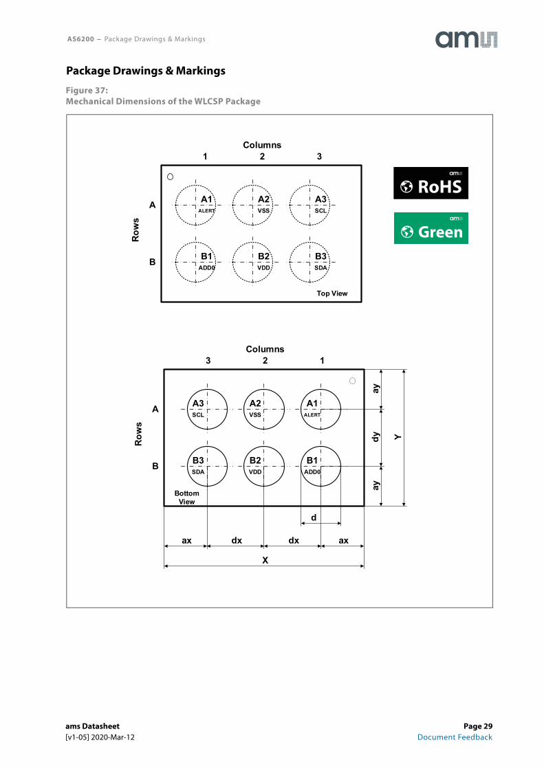
AS6200 − Package Drawings & Markings
Figure 37:Mechanical Dimensions of the WLCSP Package
Package Drawings & Markings
A
B
Row
s
3 2 1Columns
A3 A2 A1
B3 B2 B1
dx
X
Ydy
d
ax
ay
dx ax
ay
Bottom View
SCL VSS ALERT
SDA VDD ADD0
A
B
Row
s
1 2 3Columns
A3A2A1
B3B2B1
Top View
SCLVSSALERT
SDAVDDADD0
Green
RoHS
ams Datasheet Page 29[v1-05] 2020-Mar-12 Document Feedback
AS6200 − Package Drawings & Mark ings
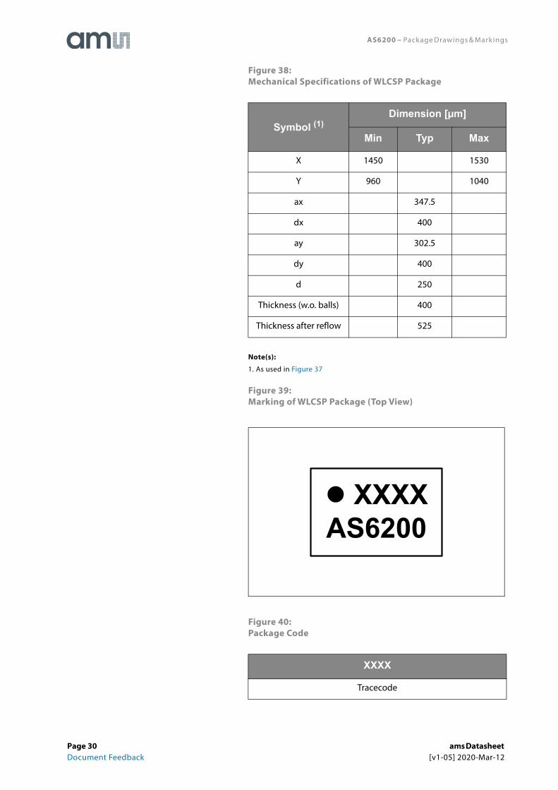
Figure 38:Mechanical Specifications of WLCSP Package
Note(s):
1. As used in Figure 37
Figure 39:Marking of WLCSP Package (Top View)
Figure 40:Package Code
Symbol (1)Dimension [µm]
Min Typ Max
X 1450 1530
Y 960 1040
ax 347.5
dx 400
ay 302.5
dy 400
d 250
Thickness (w.o. balls) 400
Thickness after reflow 525
XXXX
Tracecode
� XXXXAS6200
Page 30 ams Datasheet Document Feedback [v1-05] 2020-Mar-12
AS6200 − Ordering & Contact Information
Figure 41:Ordering Information
Buy our products or get free samples online at:www.ams.com/Products
Technical Support is available at:www.ams.com/Technical-Support
Provide feedback about this document at:www.ams.com/Document-Feedback
For further information and requests, e-mail us at:[email protected]
For sales offices, distributors and representatives, please visit: www.ams.com/Contact
Headquartersams AGTobelbader Strasse 308141 PremstaettenAustria, Europe
Tel: +43 (0) 3136 500 0
Website: www.ams.com
Ordering Code Package Marking Delivery Form Delivery Quantity
AS6200-AWLT-S WLCSP AS6200 7” Tape and Reel in dry pack 500 pcs/reel
AS6200-AWLT-L WLCSP AS6200 13” Tape and Reel in dry pack 5000 pcs/reel
Ordering & Contact Information
ams Datasheet Page 31[v1-05] 2020-Mar-12 Document Feedback
AS6200 − RoHS Compliant & ams Green Statement
RoHS: The term RoHS compliant means that ams AG products fully comply with current RoHS directives. Our semiconductor products do not contain any chemicals for all 6 substance categories plus additional 4 substance categories (per amendment EU 2015/863), including the requirement that lead not exceed 0.1% by weight in homogeneous materials. Where designed to be soldered at high temperatures, RoHS compliant products are suitable for use in specified lead-free processes.
ams Green (RoHS compliant and no Sb/Br/Cl): ams Green defines that in addition to RoHS compliance, our products are free of Bromine (Br) and Antimony (Sb) based flame retardants (Br or Sb do not exceed 0.1% by weight in homogeneous material) and do not contain Chlorine (Cl not exceed 0.1% by weight in homogeneous material).
Important Information: The information provided in this statement represents ams AG knowledge and belief as of the date that it is provided. ams AG bases its knowledge and belief on information provided by third parties, and makes no representation or warranty as to the accuracy of such information. Efforts are underway to better integrate information from third parties. ams AG has taken and continues to take reasonable steps to provide representative and accurate information but may not have conducted destructive testing or chemical analysis on incoming materials and chemicals. ams AG and ams AG suppliers consider certain information to be proprietary, and thus CAS numbers and other limited information may not be available for release.
RoHS Compliant & ams Green Statement
Page 32 ams Datasheet Document Feedback [v1-05] 2020-Mar-12
AS6200 − Copyrights & Disclaimer
Copyright ams AG, Tobelbader Strasse 30, 8141 Premstaetten, Austria-Europe. Trademarks Registered. All rights reserved. The material herein may not be reproduced, adapted, merged, translated, stored, or used without the prior written consent of the copyright owner.
Devices sold by ams AG are covered by the warranty and patent indemnification provisions appearing in its General Terms of Trade. ams AG makes no warranty, express, statutory, implied, or by description regarding the information set forth herein. ams AG reserves the right to change specifications and prices at any time and without notice. Therefore, prior to designing this product into a system, it is necessary to check with ams AG for current information. This product is intended for use in commercial applications. Applications requiring extended temperature range, unusual environmental requirements, or high reliability applications, such as military, medical life-support or life-sustaining equipment are specifically not recommended without additional processing by ams AG for each application. This product is provided by ams AG “AS IS” and any express or implied warranties, including, but not limited to the implied warranties of merchantability and fitness for a particular purpose are disclaimed.
ams AG shall not be liable to recipient or any third party for any damages, including but not limited to personal injury, property damage, loss of profits, loss of use, interruption of business or indirect, special, incidental or consequential damages, of any kind, in connection with or arising out of the furnishing, performance or use of the technical data herein. No obligation or liability to recipient or any third party shall arise or flow out of ams AG rendering of technical or other services.
Copyrights & Disclaimer
ams Datasheet Page 33[v1-05] 2020-Mar-12 Document Feedback
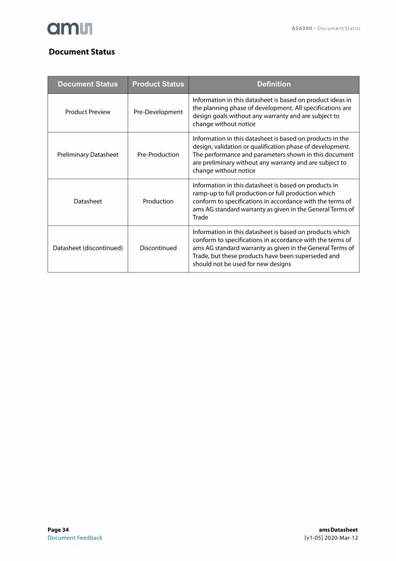
AS6200 − Document Status
Document Status Product Status Definition
Product Preview Pre-Development
Information in this datasheet is based on product ideas in the planning phase of development. All specifications are design goals without any warranty and are subject to change without notice
Preliminary Datasheet Pre-Production
Information in this datasheet is based on products in the design, validation or qualification phase of development. The performance and parameters shown in this document are preliminary without any warranty and are subject to change without notice
Datasheet Production
Information in this datasheet is based on products in ramp-up to full production or full production which conform to specifications in accordance with the terms of ams AG standard warranty as given in the General Terms of Trade
Datasheet (discontinued) Discontinued
Information in this datasheet is based on products which conform to specifications in accordance with the terms of ams AG standard warranty as given in the General Terms of Trade, but these products have been superseded and should not be used for new designs
Document Status
Page 34 ams Datasheet Document Feedback [v1-05] 2020-Mar-12
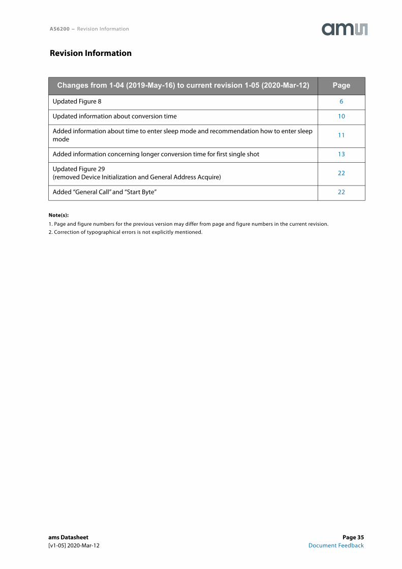
AS6200 − Revision Information
Note(s):
1. Page and figure numbers for the previous version may differ from page and figure numbers in the current revision.
2. Correction of typographical errors is not explicitly mentioned.
Changes from 1-04 (2019-May-16) to current revision 1-05 (2020-Mar-12) Page
Updated Figure 8 6
Updated information about conversion time 10
Added information about time to enter sleep mode and recommendation how to enter sleep mode
11
Added information concerning longer conversion time for first single shot 13
Updated Figure 29(removed Device Initialization and General Address Acquire)
22
Added “General Call” and “Start Byte” 22
Revision Information
ams Datasheet Page 35[v1-05] 2020-Mar-12 Document Feedback
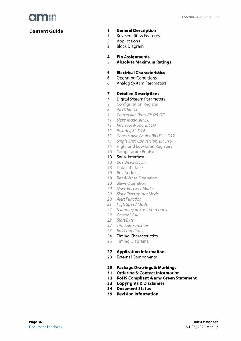
AS6200 − Content Guide
1 General Description1 Key Benefits & Features2 Applications3 Block Diagram
4 Pin Assignments5 Absolute Maximum Ratings
6 Electrical Characteristics6 Operating Conditions6 Analog System Parameters
7 Detailed Descriptions7 Digital System Parameters8 Configuration Register8 Alert, Bit D59 Conversion Rate, Bit D6-D711 Sleep Mode, Bit D811 Interrupt Mode, Bit D912 Polarity, Bit D1013 Consecutive Faults, Bits D11-D1213 Single Shot Conversion, Bit D1514 High- and Low-Limit Registers16 Temperature Register18 Serial Interface18 Bus Description18 Data Interface19 Bus Address19 Read/Write Operation20 Slave Operation20 Slave Receiver Mode20 Slave Transmitter Mode20 Alert Function21 High Speed Mode22 Summary of Bus Commands22 General Call22 Start Byte22 Timeout Function23 Bus Conditions24 Timing Characteristics25 Timing Diagrams
27 Application Information28 External Components
29 Package Drawings & Markings31 Ordering & Contact Information32 RoHS Compliant & ams Green Statement33 Copyrights & Disclaimer34 Document Status35 Revision Information
Content Guide
Page 36 ams Datasheet Document Feedback [v1-05] 2020-Mar-12