Embed Size (px)
Citation preview
AS560012-Bit Programmable Contactless Potentiometer
The AS5600 is an easy to program magnetic rotary position sensor with a high-resolution 12-bit analog or PWM output. This contactless system measures the absolute angle of a diametric magnetized on-axis magnet. This AS5600 is designed for contactless potentiometer applications and its robust design eliminates the influence of any homogenous external stray magnetic fields.
The industry-standard I²C interface supports simple user programming of non-volatile parameters without requiring a dedicated programmer.
By default the output represents a range from 0 to 360 degrees. It is also possible to define a smaller range to the output by programming a zero angle (start position) and a maximum angle (stop position).
The AS5600 is also equipped with a smart low power mode feature to automatically reduce the power consumption.
An input pin (DIR) selects the polarity of the output with regard to rotation direction. If DIR is connected to ground, the output value increases with clockwise rotation. If DIR is connected to VDD, the output value increases with counterclockwise rotation.
Ordering Information and Content Guide appear at end of datasheet.
Key Benefits & FeaturesThe benefits and features of AS5600, 12-bit Programmable Contactless Potentiometer are listed below:
Figure 1:Added Value of Using AS5600
Benefits Features
• Highest reliability and durability • Contactless angle measurement
• Simple programming• Simple user-programmable start and stop positions over the I²C
interface
• Great flexibility on angular excursion • Maximum angle programmable from 18° up to 360°
• High-resolution output signal • 12-bit DAC output resolution
• Selectable output• Analog output ratiometric to VDD or PWM-encoded digital
output
General Description
ams Datasheet Page 1[v1-06] 2018-Jun-20 Document Feedback
AS5600 − General Description
Applications The AS5600 is ideally suited for contactless potentiometers, contactless knobs, pedals, RC servos and other angular position measurement solutions.
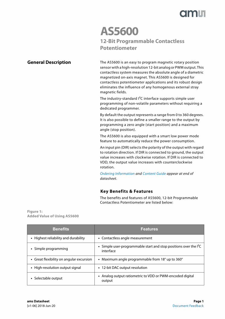
Block Diagram The functional blocks of this device are shown below:
Figure 2:Functional Blocks of AS5600
• Low-power consumption • Automatic entry into low-power mode
• Easy setup • Automatic magnet detection
• Small form factor • SOIC-8 package
• Robust environmental tolerance • Wide temperature range: -40°C to 125°C
Benefits Features
AFE
AGC
12-bit A/D Driver
Register Setting
OTP
I²C
AS5600
OUT
VDD3V3
VDD5V
GND
SCLSDA
PWM
PGO
DIR
Analog Front-EndHall Sensors
12-bit D/A
ATAN(CORDIC)
Digital Processing
and Filtering
LDO 3.3V
Magnetic Core
Page 2 ams Datasheet Document Feedback [v1-06] 2018-Jun-20
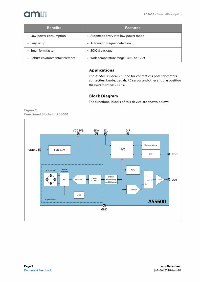
AS5600 − Pin Assignments
Figure 3:SOIC-8 Pin-Out
Figure 4:Pin Description
Pin Number Name Type Description
1 VDD5V SupplyPositive voltage supply in 5V mode (requires 100nF decoupling capacitor)
2 VDD3V3 SupplyPositive voltage supply in 3.3V mode (requires an external 1-μF decoupling capacitor in 5V mode)
3 OUT Analog/digital output Analog/PWM output
4 GND Supply Ground
5 PGO Digital inputProgram option (internal pull-up, connected toGND = Programming Option B)
6 SDA Digital input/output I²C Data (consider external pull-up)
7 SCL Digital input I²C Clock (consider external pull-up)
8 DIR Digital inputDirection polarity (GND = values increase clockwise, VDD = values increase counterclockwise)
Pin Assignments
2
3
4 5
6
7
81
VDD3V3
OUT
GND
VDD5V
PGO
SDA
SCL
DIR
AS5
600
ams Datasheet Page 3[v1-06] 2018-Jun-20 Document Feedback
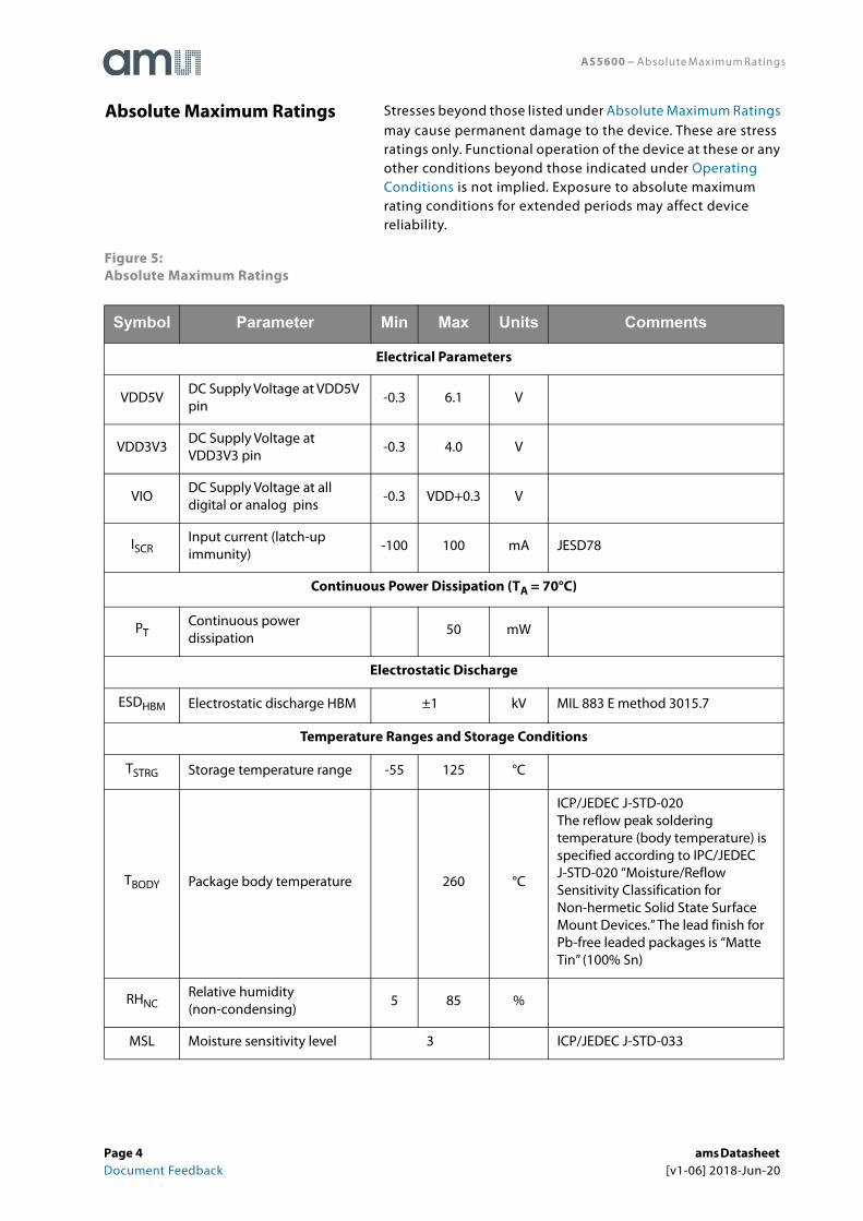
AS5600 − Absolute Maximum Ratings
Stresses beyond those listed under Absolute Maximum Ratings may cause permanent damage to the device. These are stress ratings only. Functional operation of the device at these or any other conditions beyond those indicated under Operating Conditions is not implied. Exposure to absolute maximum rating conditions for extended periods may affect device reliability.
Figure 5:Absolute Maximum Ratings
Symbol Parameter Min Max Units Comments
Electrical Parameters
VDD5VDC Supply Voltage at VDD5V pin
-0.3 6.1 V
VDD3V3DC Supply Voltage at VDD3V3 pin
-0.3 4.0 V
VIODC Supply Voltage at all digital or analog pins
-0.3 VDD+0.3 V
ISCRInput current (latch-up immunity)
-100 100 mA JESD78
Continuous Power Dissipation (TA = 70°C)
PTContinuous power dissipation
50 mW
Electrostatic Discharge
ESDHBM Electrostatic discharge HBM ±1 kV MIL 883 E method 3015.7
Temperature Ranges and Storage Conditions
TSTRG Storage temperature range -55 125 °C
TBODY Package body temperature 260 °C
ICP/JEDEC J-STD-020The reflow peak soldering temperature (body temperature) is specified according to IPC/JEDEC J-STD-020 “Moisture/Reflow Sensitivity Classification for Non-hermetic Solid State Surface Mount Devices.” The lead finish for Pb-free leaded packages is “Matte Tin” (100% Sn)
RHNCRelative humidity (non-condensing)
5 85 %
MSL Moisture sensitivity level 3 ICP/JEDEC J-STD-033
Absolute Maximum Ratings
Page 4 ams Datasheet Document Feedback [v1-06] 2018-Jun-20
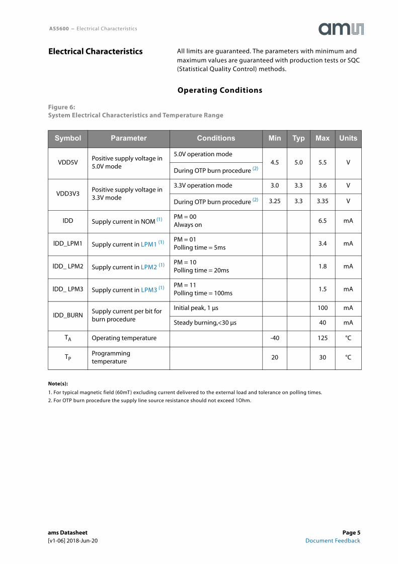
AS5600 − Electrical Characteristics
All limits are guaranteed. The parameters with minimum and maximum values are guaranteed with production tests or SQC (Statistical Quality Control) methods.
Operating Conditions
Figure 6:System Electrical Characteristics and Temperature Range
Note(s):
1. For typical magnetic field (60mT) excluding current delivered to the external load and tolerance on polling times.
2. For OTP burn procedure the supply line source resistance should not exceed 1Ohm.
Symbol Parameter Conditions Min Typ Max Units
VDD5VPositive supply voltage in 5.0V mode
5.0V operation mode4.5 5.0 5.5 V
During OTP burn procedure (2)
VDD3V3Positive supply voltage in 3.3V mode
3.3V operation mode 3.0 3.3 3.6 V
During OTP burn procedure (2) 3.25 3.3 3.35 V
IDD Supply current in NOM (1) PM = 00Always on
6.5 mA
lDD_LPM1 Supply current in LPM1 (1) PM = 01Polling time = 5ms
3.4 mA
lDD_ LPM2 Supply current in LPM2 (1) PM = 10Polling time = 20ms
1.8 mA
lDD_ LPM3 Supply current in LPM3 (1) PM = 11Polling time = 100ms
1.5 mA
IDD_BURNSupply current per bit for burn procedure
Initial peak, 1 μs 100 mA
Steady burning,<30 μs 40 mA
TA Operating temperature -40 125 °C
TPProgramming temperature
20 30 °C
Electrical Characteristics
ams Datasheet Page 5[v1-06] 2018-Jun-20 Document Feedback
AS5600 − Electrical Characteristics
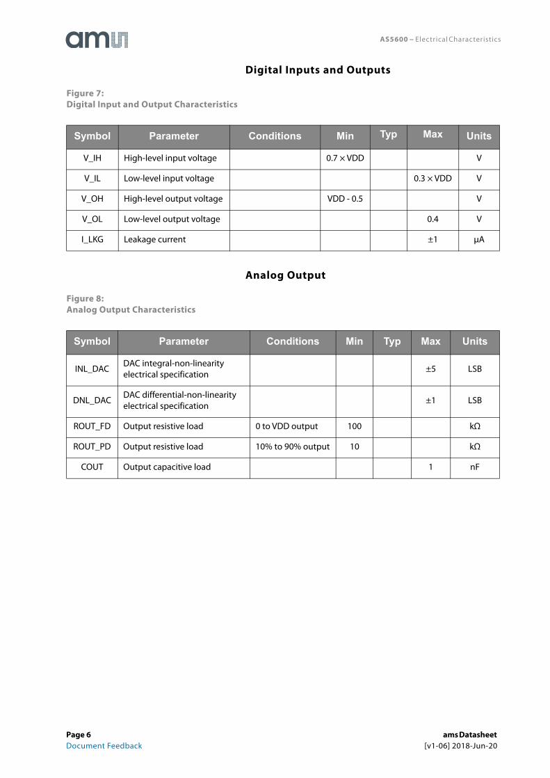
Digital Inputs and Outputs
Figure 7:Digital Input and Output Characteristics
Analog Output
Figure 8:Analog Output Characteristics
Symbol Parameter Conditions Min Typ Max Units
V_IH High-level input voltage 0.7 × VDD V
V_IL Low-level input voltage 0.3 × VDD V
V_OH High-level output voltage VDD - 0.5 V
V_OL Low-level output voltage 0.4 V
I_LKG Leakage current ±1 μA
Symbol Parameter Conditions Min Typ Max Units
INL_DACDAC integral-non-linearity electrical specification
±5 LSB
DNL_DACDAC differential-non-linearity electrical specification
±1 LSB
ROUT_FD Output resistive load 0 to VDD output 100 kΩ
ROUT_PD Output resistive load 10% to 90% output 10 kΩ
COUT Output capacitive load 1 nF
Page 6 ams Datasheet Document Feedback [v1-06] 2018-Jun-20
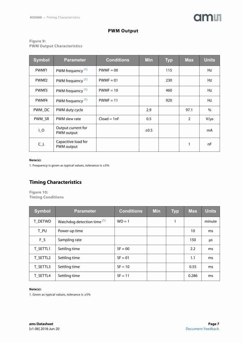
AS5600 − Timing Characteristics
PWM Output
Figure 9:PWM Output Characteristics
Note(s):
1. Frequency is given as typical values, tolerance is ±5%
Figure 10:Timing Conditions
Note(s):
1. Given as typical values, tolerance is ±5%
Symbol Parameter Conditions Min Typ Max Units
PWMf1 PWM frequency (1) PWMF = 00 115 Hz
PWMf2 PWM frequency (1) PWMF = 01 230 Hz
PWMf3 PWM frequency (1) PWMF = 10 460 Hz
PWMf4 PWM frequency (1) PWMF = 11 920 Hz
PWM_DC PWM duty cycle 2.9 97.1 %
PWM_SR PWM slew rate Cload = 1nF 0.5 2 V/μs
I_OOutput current for PWM output
±0.5 mA
C_LCapacitive load for PWM output
1 nF
Symbol Parameter Conditions Min Typ Max Units
T_DETWD Watchdog detection time (1) WD = 1 1 minute
T_PU Power-up time 10 ms
F_S Sampling rate 150 μs
T_SETTL1 Settling time SF = 00 2.2 ms
T_SETTL2 Settling time SF = 01 1.1 ms
T_SETTL3 Settling time SF = 10 0.55 ms
T_SETTL4 Settling time SF = 11 0.286 ms
Timing Characteristics
ams Datasheet Page 7[v1-06] 2018-Jun-20 Document Feedback
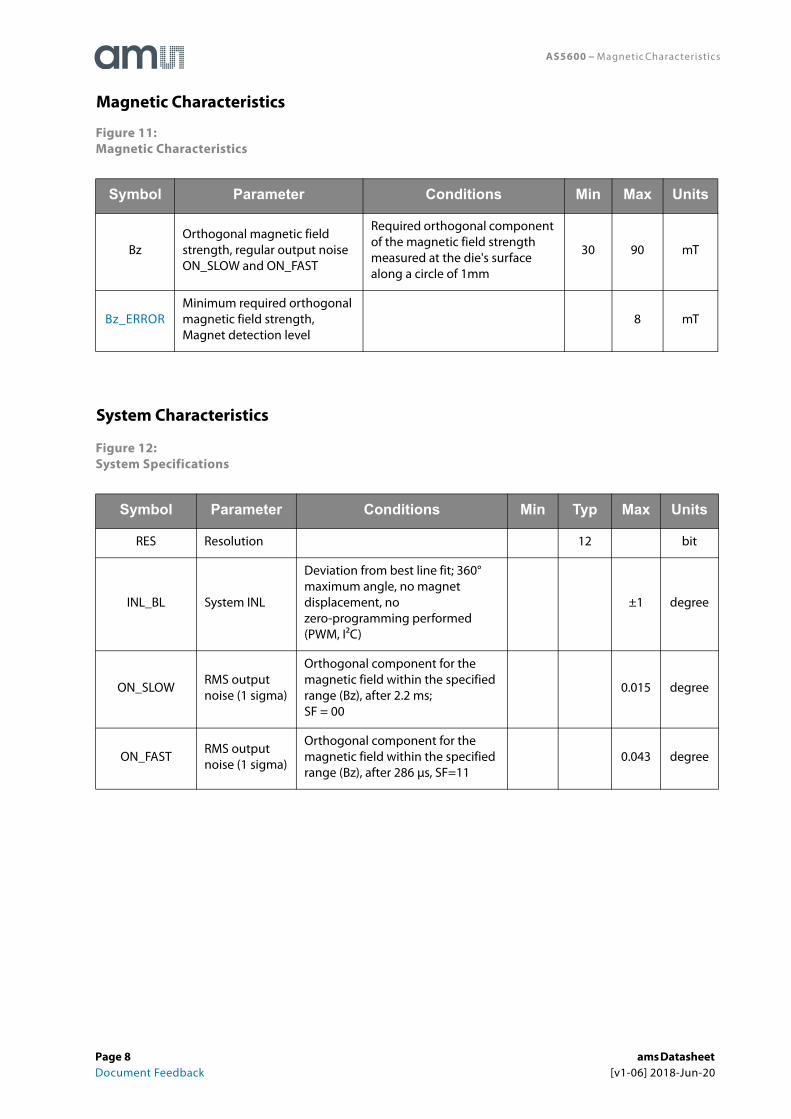
AS5600 − Magnetic Characteristics
Figure 11:Magnetic Characteristics
Figure 12:System Specifications
Symbol Parameter Conditions Min Max Units
BzOrthogonal magnetic field strength, regular output noise ON_SLOW and ON_FAST
Required orthogonal component of the magnetic field strength measured at the die's surface along a circle of 1mm
30 90 mT
Bz_ERRORMinimum required orthogonal magnetic field strength, Magnet detection level
8 mT
Symbol Parameter Conditions Min Typ Max Units
RES Resolution 12 bit
INL_BL System INL
Deviation from best line fit; 360° maximum angle, no magnet displacement, no zero-programming performed (PWM, I²C)
±1 degree
ON_SLOWRMS output noise (1 sigma)
Orthogonal component for the magnetic field within the specified range (Bz), after 2.2 ms;SF = 00
0.015 degree
ON_FASTRMS output noise (1 sigma)
Orthogonal component for the magnetic field within the specified range (Bz), after 286 μs, SF=11
0.043 degree
Magnetic Characteristics
System Characteristics
Page 8 ams Datasheet Document Feedback [v1-06] 2018-Jun-20
AS5600 − Detailed Description
The AS5600 is a Hall-based rotary magnetic position sensor using planar sensors that convert the magnetic field component perpendicular to the surface of the chip into a voltage.
The signals coming from the Hall sensors are first amplified and filtered before being converted by the analog-to-digital converter (ADC). The output of the ADC is processed by the hardwired CORDIC block (Coordinate Rotation Digital Computer) to compute the angle and magnitude of the magnetic field vector. The intensity of the magnetic field is used by the automatic gain control (AGC) to adjust the amplification level to compensate for temperature and magnetic field variations.
The angle value provided by the CORDIC algorithm is used by the output stage. The user can choose between an analog output and a PWM-encoded digital output. The former provides an output voltage which represents the angle as a ratiometric linear absolute value. The latter provides a digital output which represents the angle as the pulse width.
The AS5600 is programmed through an industry-standard I²C interface to write an on-chip non-volatile memory. This interface can be used to program a zero angle (start position) and a maximum angle (stop position) which maps the full resolution of the output to a subset of the entire 0 to 360 degree range.
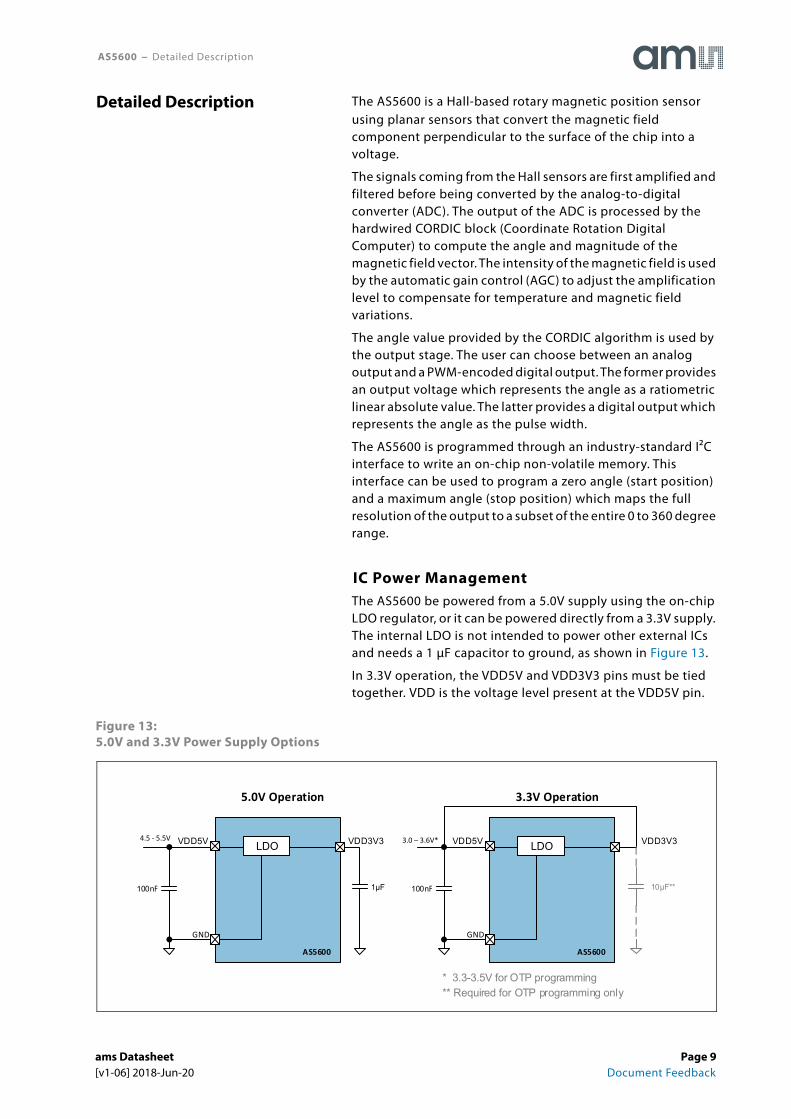
IC Power ManagementThe AS5600 be powered from a 5.0V supply using the on-chip LDO regulator, or it can be powered directly from a 3.3V supply. The internal LDO is not intended to power other external ICs and needs a 1 μF capacitor to ground, as shown in Figure 13.
In 3.3V operation, the VDD5V and VDD3V3 pins must be tied together. VDD is the voltage level present at the VDD5V pin.
Figure 13:5.0V and 3.3V Power Supply Options
Detailed Description
1µF100nF
4.5 - 5.5V VDD3V3
GND
VDD5V
5.0V Operation
LDO
AS5600
100nF
3.0 – 3.6V* VDD3V3
GND
VDD5V
3.3V Operation
LDO
AS5600
10µF**
** Required for OTP programming only* 3.3-3.5V for OTP programming
ams Datasheet Page 9[v1-06] 2018-Jun-20 Document Feedback
AS5600 − Detailed Description
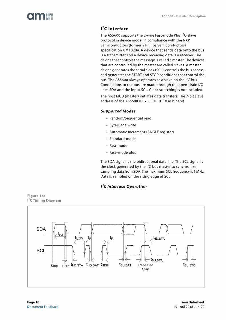
I²C InterfaceThe AS5600 supports the 2-wire Fast-mode Plus I²C-slave protocol in device mode, in compliance with the NXP Semiconductors (formerly Philips Semiconductors) specification UM10204. A device that sends data onto the bus is a transmitter and a device receiving data is a receiver. The device that controls the message is called a master. The devices that are controlled by the master are called slaves. A master device generates the serial clock (SCL), controls the bus access, and generates the START and STOP conditions that control the bus. The AS5600 always operates as a slave on the I²C bus. Connections to the bus are made through the open-drain I/O lines SDA and the input SCL. Clock stretching is not included.
The host MCU (master) initiates data transfers. The 7-bit slave address of the AS5600 is 0x36 (0110110 in binary).
Supported Modes
• Random/Sequential read
• Byte/Page write
• Automatic increment (ANGLE register)
• Standard-mode
• Fast-mode
• Fast–mode plus
The SDA signal is the bidirectional data line. The SCL signal is the clock generated by the I²C bus master to synchronize sampling data from SDA. The maximum SCL frequency is 1 MHz. Data is sampled on the rising edge of SCL.
I²C Interface Operation
Figure 14:I²C Timing Diagram
SDA
SCL
StartStop
tbuftLOW tR
tHD.STA tHIGH
tF
tSU.DAT
tSU.STA
tHD.STA
tSU.STORepeatedStart
tHD.DAT
Page 10 ams Datasheet Document Feedback [v1-06] 2018-Jun-20
AS5600 − Detailed Description
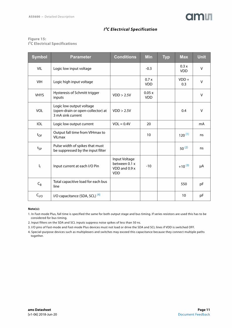
I²C Electrical Specification
Figure 15:I²C Electrical Specifications
Note(s):
1. In Fast-mode Plus, fall time is specified the same for both output stage and bus timing. If series resistors are used this has to be considered for bus timing.
2. Input filters on the SDA and SCL inputs suppress noise spikes of less than 50 ns.
3. I/O pins of Fast-mode and Fast-mode Plus devices must not load or drive the SDA and SCL lines if VDD is switched OFF.
4. Special-purpose devices such as multiplexers and switches may exceed this capacitance because they connect multiple paths together.
Symbol Parameter Conditions Min Typ Max Unit
VIL Logic low input voltage -0.30.3 x VDD
V
VIH Logic high input voltage0.7 x VDD
VDD + 0.3
V
VHYSHysteresis of Schmitt trigger inputs
VDD > 2.5V0.05 x VDD
V
VOLLogic low output voltage (open-drain or open-collector) at 3 mA sink current
VDD > 2.5V 0.4 V
IOL Logic low output current VOL = 0.4V 20 mA
tOFOutput fall time from VIHmax to VILmax
10 120 (1) ns
tSPPulse width of spikes that must be suppressed by the input filter 50 (2) ns
II Input current at each I/O Pin
Input Voltage between 0.1 x VDD and 0.9 x VDD
-10 +10 (3) μA
CBTotal capacitive load for each bus line
550 pF
CI/O I/O capacitance (SDA, SCL) (4) 10 pF
ams Datasheet Page 11[v1-06] 2018-Jun-20 Document Feedback
AS5600 − Detailed Description
I²C Timing
Figure 16:I²C Timing
Note(s):
1. After this time, the first clock is generated.
2. A device must internally provide a minimum hold time of 120 ns (Fast-mode Plus) for the SDA signal (referred to the VIHmin of SCL) to bridge the undefined region of the falling edge of SCL.
3. A Fast-mode device can be used in a standard-mode system, but the requirement tSU;DAT = 250 ns must be met. This is automatically if the device does not stretch the low phase of SCL. If such a device does stretch the low phase of SCL, it must drive the next data bit on SDA (tRmax + tSU;DAT = 1000 + 250 = 1250 ns) before SCL is released.
4. In Fast-mode Plus, fall time is specified the same for both output stage and bus timing. If series resistors are used, this has to be considered for bus timing.
Symbol Parameter Min Max Unit
fSCLK SCL clock frequency 1.0 MHz
tBUFBus free time (time between the STOP and START conditions)
0.5 μs
tHD;STA Hold time; (Repeated) START condition (1) 0.26 μs
tLOW Low phase of SCL clock 0.5 μs
tHIGH High phase of SCL clock 0.26 μs
tSU;STA Setup time for a Repeated START condition 0.26 μs
tHD;DAT Data hold time (2) 0.45 μs
tSU;DAT Data setup time (3) 50 ns
tR Rise time of SDA and SCL signals 120 ns
tF Fall time of SDA and SCL signals 10 120 (4) ns
tSU;STO Setup time for STOP condition 0.26 μs
Page 12 ams Datasheet Document Feedback [v1-06] 2018-Jun-20
AS5600 − Detailed Description
I²C Modes
Invalid Addresses
There are two addresses used to access an AS5600 register. The first is the slave address used to select the AS5600. All I²C bus transactions include a slave address. The slave address of the AS5600 is 0x36 (0110110 in binary) The second address is a word address sent in the first byte transferred in a write transaction. The word address selects a register on the AS5600. The word address is loaded into the address pointer on the AS5600. During subsequent read transactions and subsequent bytes in the write transaction, the address pointer provides the address of the selected register. The address pointer is incremented after each byte is transferred, except for certain read transactions to special registers.
If the user sets the address pointer to an invalid word address, the address byte is not acknowledged (the A bit is high). Nevertheless, a read or write cycle is possible. The address pointer is increased after each byte.
Reading
When reading from an invalid address, the AS5600 returns all zeros in the data bytes. The address pointer is incremented after each byte. Sequential reads over the whole address range are possible including address overflow.
Automatic Increment of the Address Pointer for ANGLE, RAW ANGLE and MAGNITUDE Registers
These are special registers which suppress the automatic increment of the address pointer on reads, so a re-read of these registers requires no I²C write command to reload the address pointer. This special treatment of the pointer is effective only if the address pointer is set to the high byte of the register.
Writing
A write to an invalid address is not acknowledged by the AS5600, although the address pointer is incremented. When the address pointer points to a valid address again, a successful write accessed is acknowledged. Page write over the whole address range is possible including address overflow.
Supported Bus Protocol
Data transfer may be initiated only when the bus is not busy.
During data transfer, the data line must remain stable whenever SCL is high. Changes in the data line while SCL is high are interpreted as START or STOP conditions.
ams Datasheet Page 13[v1-06] 2018-Jun-20 Document Feedback
AS5600 − Detailed Description
Accordingly, the following bus conditions have been defined:
Bus Not Busy
Both SDA and SCL remain high.
Start Data Transfer
A change in the state of SDA from high to low while SCL is high defines the START condition.
Stop Data Transfer
A change in the state of SDA from low to high while SCL is high defines the STOP condition.
Data Valid
The state of the data line represents valid data when, after a START condition, SDA is stable for the duration of the high phase of SCL. The data on SDA must be changed during the low phase of SCL. There is one clock period per bit of data.
Each I²C bus transaction is initiated with a START condition and terminated with a STOP condition. The number of data bytes transferred between START and STOP conditions is not limited, and is determined by the I²C bus master. The information is transferred byte-wise and each receiver acknowledges with a ninth bit.
Acknowledge
Each I²C slave device, when addressed, is obliged to generate an acknowledge after the reception of each byte. The I²C bus master device must generate an extra clock period for this acknowledge bit.
A slave that acknowledges must pull down SDA during the acknowledge clock period in such a way that SDA is stable low during the high phase of the acknowledge clock period. Of course, setup and hold times must be taken into account. A master must signal an end of a read transaction by not generating an acknowledge bit on the last byte that has been clocked out of the slave. In this case, the slave must leave SDA high to enable the master to generate the STOP condition.
Figure 17:Data Read
1 ...19876...2 987
SDA
SCL
StartCondition
Stop Condition or Repeated Start Condition
MSB R/W ACKLSB ACK
Slave Address Repeated if more Bytes are transferred
Page 14 ams Datasheet Document Feedback [v1-06] 2018-Jun-20
AS5600 − Detailed Description
Depending on the state of the R/W bit, two types of data transfer are possible:
Data Transfer from a Master Transmitter to a Slave Receiver
The first byte transmitted by the master is the slave address, followed by R/W = 0. Next follows a number of data bytes. The slave returns an acknowledge bit after each received byte. If the slave does not understand the command or data it sends a not acknowledge (NACK). Data is transferred with the most significant bit (MSB) first.
Data Transfer from a Slave Transmitter to a Master Receiver
The master transmits the first byte (the slave address). The slave then returns an acknowledge bit, followed by the slave transmitting a number of data bytes. The master returns an acknowledge bit after all received bytes other than the last byte. At the end of the last received byte, a NACK is returned. The master generates all of the SCL clock periods and the START and STOP conditions. A transfer is ended with a STOP condition or with a repeated START condition. Because a repeated START condition is also the beginning of the next serial transfer, the bus is not released. Data is transferred with the most significant bit (MSB) first.
AS5600 Slave Modes
Slave Receiver Mode (Write Mode)
Serial data and clock are received through SDA and SCL. Each byte is followed by an acknowledge bit or by a not acknowledge depending on whether the address-pointer selects a valid address. START and STOP conditions are recognized as the beginning and end of a bus transaction. The slave address byte is the first byte received after the START condition. The 7-bit AS5600 address is 0x36 (0110110 in binary).
The 7-bit slave address is followed by the direction bit (R/W), which, for a write, is 0 (low). After receiving and decoding the slave address byte the slave device drives an acknowledge on SDA. After the AS5600 acknowledges the slave address and write bit, the master transmits a register address (word address) to the AS5600. This is loaded into the address pointer on the AS5600. If the address is a valid readable address, the AS5600 answers by sending an acknowledge (A bit low). If the address pointer selects an invalid address, a not acknowledge is sent (A bit high). The master may then transmit zero or more bytes of data. If the address pointer selects an invalid address, the received data are not stored. The address pointer will increment after each byte transferred whether or not the address is valid. If the address-pointer reaches a valid position again, the AS5600 answers with an acknowledge and stores the data. The master generates a STOP condition to terminate the write transaction.
ams Datasheet Page 15[v1-06] 2018-Jun-20 Document Feedback
AS5600 − Detailed Description
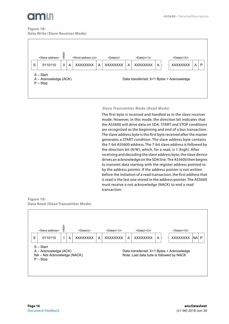
Figure 18:Data Write (Slave Receiver Mode)
Slave Transmitter Mode (Read Mode)
The first byte is received and handled as in the slave receiver mode. However, in this mode, the direction bit indicates that the AS5600 will drive data on SDA. START and STOP conditions are recognized as the beginning and end of a bus transaction. The slave address byte is the first byte received after the master generates a START condition. The slave address byte contains the 7-bit AS5600 address. The 7-bit slave address is followed by the direction bit (R/W), which, for a read, is 1 (high). After receiving and decoding the slave address byte, the slave device drives an acknowledge on the SDA line. The AS5600 then begins to transmit data starting with the register address pointed to by the address pointer. If the address pointer is not written before the initiation of a read transaction, the first address that is read is the last one stored in the address pointer. The AS5600 must receive a not acknowledge (NACK) to end a read transaction.
Figure 19:Data Read (Slave Transmitter Mode)
S 0110110 0 A XXXXXXXX A XXXXXXXX A XXXXXXXX A
S – StartA – Acknowledge (ACK) Data transferred: X+1 Bytes + AcknowledgeP – Stop
P
<Slave address> <Word address (n)> <Data(n)> <Data(n+X)><RW
>XXXXXXXX A
<Data(n+1)>
S 0110110 1 A XXXXXXXX A XXXXXXXX A XXXXXXXX NA
S – StartA – Acknowledge (ACK) Data transferred: X+1 Bytes + AcknowledgeNA – Not Acknowledge (NACK) Note: Last data byte is followed by NACKP – Stop
P
<Slave address> <Data(n)> <Data(n+1)> <Data(n+X)><RW
>
XXXXXXXX A
<Data(n+2)>
Page 16 ams Datasheet Document Feedback [v1-06] 2018-Jun-20
AS5600 − Detailed Description
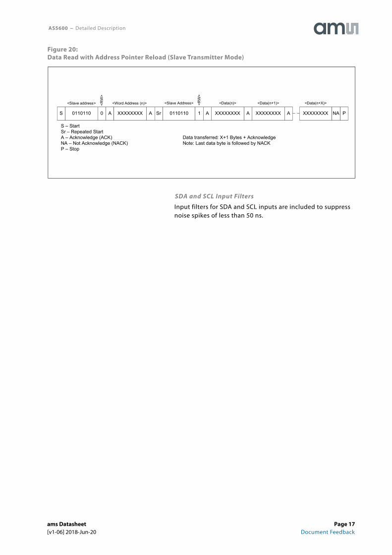
Figure 20:Data Read with Address Pointer Reload (Slave Transmitter Mode)
SDA and SCL Input Filters
Input filters for SDA and SCL inputs are included to suppress noise spikes of less than 50 ns.
S 0110110 0 A XXXXXXXX A 0110110 1 XXXXXXXXA
S – StartSr – Repeated StartA – Acknowledge (ACK) Data transferred: X+1 Bytes + AcknowledgeNA – Not Acknowledge (NACK) Note: Last data byte is followed by NACKP – Stop
P
<Slave address> <Word Address (n)> <Slave Address> <Data(n+1)><RW
>
XXXXXXXXA
<Data(n)>
Sr
<RW
>
A XXXXXXXX NA
<Data(n+X)>
ams Datasheet Page 17[v1-06] 2018-Jun-20 Document Feedback
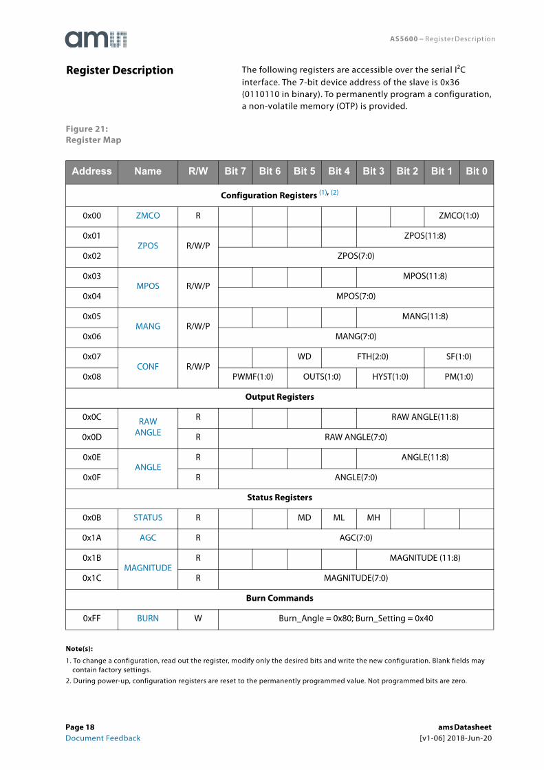
AS5600 − Register Description
The following registers are accessible over the serial I²C interface. The 7-bit device address of the slave is 0x36(0110110 in binary). To permanently program a configuration, a non-volatile memory (OTP) is provided.
Figure 21:Register Map
Note(s):
1. To change a configuration, read out the register, modify only the desired bits and write the new configuration. Blank fields may contain factory settings.
2. During power-up, configuration registers are reset to the permanently programmed value. Not programmed bits are zero.
Address Name R/W Bit 7 Bit 6 Bit 5 Bit 4 Bit 3 Bit 2 Bit 1 Bit 0
Configuration Registers (1), (2)
0x00 ZMCO R ZMCO(1:0)
0x01ZPOS R/W/P
ZPOS(11:8)
0x02 ZPOS(7:0)
0x03MPOS R/W/P
MPOS(11:8)
0x04 MPOS(7:0)
0x05MANG R/W/P
MANG(11:8)
0x06 MANG(7:0)
0x07CONF R/W/P
WD FTH(2:0) SF(1:0)
0x08 PWMF(1:0) OUTS(1:0) HYST(1:0) PM(1:0)
Output Registers
0x0C RAWANGLE
R RAW ANGLE(11:8)
0x0D R RAW ANGLE(7:0)
0x0EANGLE
R ANGLE(11:8)
0x0F R ANGLE(7:0)
Status Registers
0x0B STATUS R MD ML MH
0x1A AGC R AGC(7:0)
0x1BMAGNITUDE
R MAGNITUDE (11:8)
0x1C R MAGNITUDE(7:0)
Burn Commands
0xFF BURN W Burn_Angle = 0x80; Burn_Setting = 0x40
Register Description
Page 18 ams Datasheet Document Feedback [v1-06] 2018-Jun-20
AS5600 − Register Description
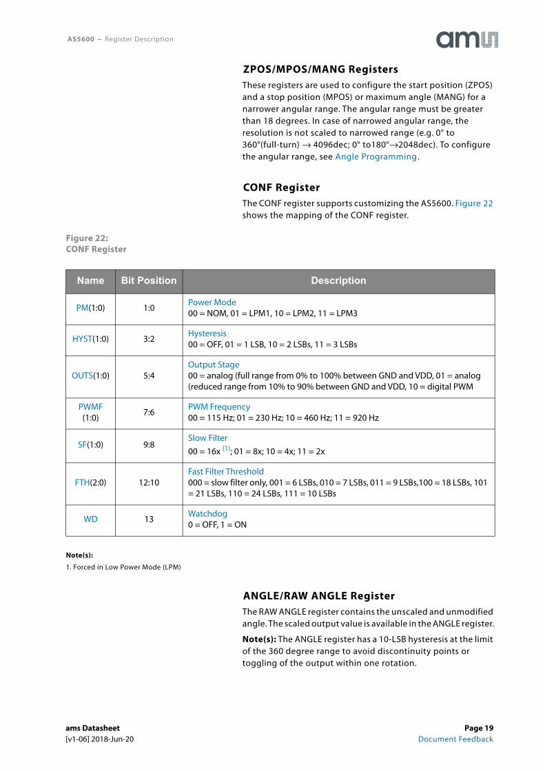
ZPOS/MPOS/MANG RegistersThese registers are used to configure the start position (ZPOS) and a stop position (MPOS) or maximum angle (MANG) for a narrower angular range. The angular range must be greater than 18 degrees. In case of narrowed angular range, the resolution is not scaled to narrowed range (e.g. 0° to 360°(full-turn) → 4096dec; 0° to180°→2048dec). To configure the angular range, see Angle Programming.
CONF RegisterThe CONF register supports customizing the AS5600. Figure 22 shows the mapping of the CONF register.
Figure 22:CONF Register
Note(s):
1. Forced in Low Power Mode (LPM)
ANGLE/RAW ANGLE RegisterThe RAW ANGLE register contains the unscaled and unmodified angle. The scaled output value is available in the ANGLE register.
Note(s): The ANGLE register has a 10-LSB hysteresis at the limit of the 360 degree range to avoid discontinuity points or toggling of the output within one rotation.
Name Bit Position Description
PM(1:0) 1:0Power Mode00 = NOM, 01 = LPM1, 10 = LPM2, 11 = LPM3
HYST(1:0) 3:2Hysteresis00 = OFF, 01 = 1 LSB, 10 = 2 LSBs, 11 = 3 LSBs
OUTS(1:0) 5:4Output Stage00 = analog (full range from 0% to 100% between GND and VDD, 01 = analog (reduced range from 10% to 90% between GND and VDD, 10 = digital PWM
PWMF(1:0)
7:6PWM Frequency00 = 115 Hz; 01 = 230 Hz; 10 = 460 Hz; 11 = 920 Hz
SF(1:0) 9:8Slow Filter00 = 16x (1); 01 = 8x; 10 = 4x; 11 = 2x
FTH(2:0) 12:10Fast Filter Threshold000 = slow filter only, 001 = 6 LSBs, 010 = 7 LSBs, 011 = 9 LSBs,100 = 18 LSBs, 101 = 21 LSBs, 110 = 24 LSBs, 111 = 10 LSBs
WD 13Watchdog0 = OFF, 1 = ON
ams Datasheet Page 19[v1-06] 2018-Jun-20 Document Feedback
AS5600 − Register Description
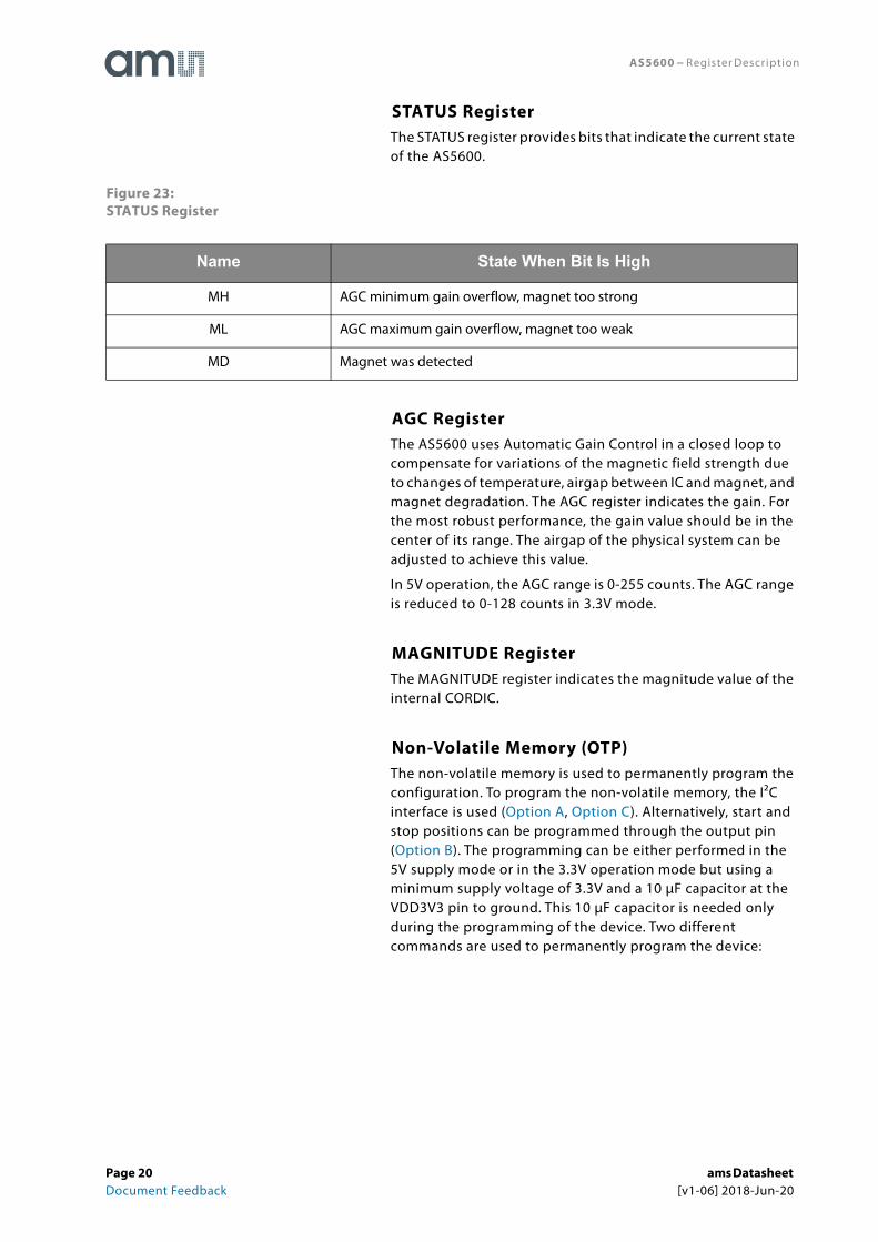
STATUS RegisterThe STATUS register provides bits that indicate the current state of the AS5600.
Figure 23:STATUS Register
AGC RegisterThe AS5600 uses Automatic Gain Control in a closed loop to compensate for variations of the magnetic field strength due to changes of temperature, airgap between IC and magnet, and magnet degradation. The AGC register indicates the gain. For the most robust performance, the gain value should be in the center of its range. The airgap of the physical system can be adjusted to achieve this value.
In 5V operation, the AGC range is 0-255 counts. The AGC range is reduced to 0-128 counts in 3.3V mode.
MAGNITUDE RegisterThe MAGNITUDE register indicates the magnitude value of the internal CORDIC.
Non-Volatile Memory (OTP)The non-volatile memory is used to permanently program the configuration. To program the non-volatile memory, the I²C interface is used (Option A, Option C). Alternatively, start and stop positions can be programmed through the output pin (Option B). The programming can be either performed in the 5V supply mode or in the 3.3V operation mode but using a minimum supply voltage of 3.3V and a 10 μF capacitor at the VDD3V3 pin to ground. This 10 μF capacitor is needed only during the programming of the device. Two different commands are used to permanently program the device:
Name State When Bit Is High
MH AGC minimum gain overflow, magnet too strong
ML AGC maximum gain overflow, magnet too weak
MD Magnet was detected
Page 20 ams Datasheet Document Feedback [v1-06] 2018-Jun-20
AS5600 − Register Description
Burn_Angle Command (ZPOS, MPOS)The host microcontroller can perform a permanent programming of ZPOS and MPOS with a BURN_ANGLE command. To perform a BURN_ANGLE command, write the value 0x80 into register 0xFF. The BURN_ANGLE command can be executed up to 3 times. ZMCO shows how many times ZPOS and MPOS have been permanently written.
This command may only be executed if the presence of the magnet is detected (MD = 1).
Burn_Setting Command (MANG, CONFIG)The host microcontroller can perform a permanent writing of MANG and CONFIG with a BURN_SETTING command. To perform a BURN_SETTING command, write the value 0x40 into register 0xFF.
MANG can be written only if ZPOS and MPOS have never been permanently written (ZMCO = 00). The BURN_ SETTING command can be performed only one time.
Angle ProgrammingFor applications which do not use the full 0 to 360 degree angular range, the output resolution can be enhanced by programming the range which is actually used. In this case, the full resolution of the output is automatically scaled to the programmed angular range. The angular range must be greater than 18 degrees.
The range is specified by programming a start position (ZPOS) and either a stop position (MPOS) or the size of the angular range (MANG).
The BURN_ANGLE command can be executed up to 3 times.
ams Datasheet Page 21[v1-06] 2018-Jun-20 Document Feedback
AS5600 − Register Description
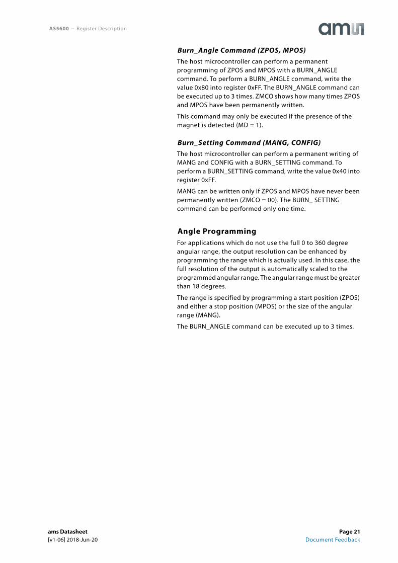
There are three recommended methods for programming the angular range:
• Option A: Angle Programming Through the I²C Interface
• Option B: Angle Programming Through the OUT Pin
• Option C: Programming a Maximum Angular Range Through the I²C Interface
Figure 24:Option A: Angle Programming Through the I²C Interface
Note(s):
1. After each register command, the new setting is effective at the output at least 1 ms later.
2. It is highly recommended to perform a functional test after this procedure.
Use the correct hardware configuration shown in Figure 37 and Figure 38.
Step 1 Power up the AS5600.
Step 2 Turn the magnet to the start position.
Step 3Read the RAW ANGLE register.Write the RAW ANGLE value into the ZPOS register.Wait at least 1 ms.
Step 4Rotate the magnet in the direction defined by the level on the DIR pin (GND for clockwise, VDD for counterclockwise) to the stop position. The amount of rotation must be greater than 18 degrees.
Step 5Read the RAW ANGLE register.Write the RAW ANGLE value into the MPOS register.Wait at least 1 ms.
Proceed with Step 6 to permanently program the configuration.
Step 6Perform a BURN_ANGLE command to permanently program the device.Wait at least 1 ms.
Step 7
Verify the BURN_ANGLE command: Write the commands 0x01, 0x11 and 0x10 sequentially into the register 0xFF to load the actual OTP content. Read the ZPOS and MPOS registers to verify that the BURN_ANGLE command was successful.
Step 8 Read and verify the ZPOS and MPOS registers again after a new power-up cycle.
Page 22 ams Datasheet Document Feedback [v1-06] 2018-Jun-20
AS5600 − Register Description
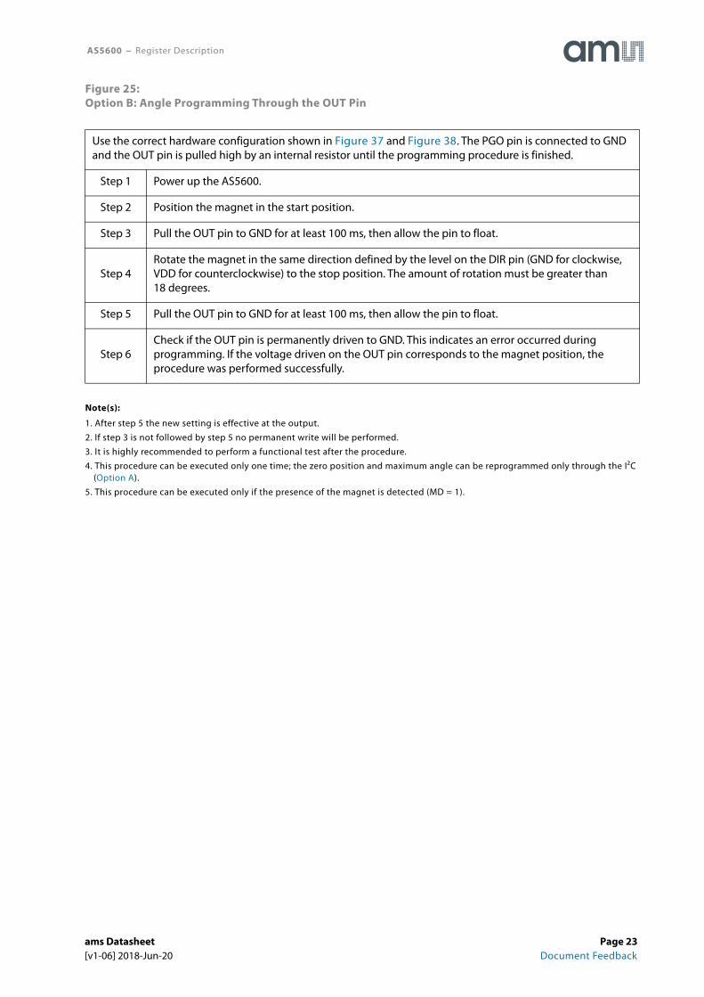
Figure 25:Option B: Angle Programming Through the OUT Pin
Note(s):
1. After step 5 the new setting is effective at the output.
2. If step 3 is not followed by step 5 no permanent write will be performed.
3. It is highly recommended to perform a functional test after the procedure.
4. This procedure can be executed only one time; the zero position and maximum angle can be reprogrammed only through the I²C (Option A).
5. This procedure can be executed only if the presence of the magnet is detected (MD = 1).
Use the correct hardware configuration shown in Figure 37 and Figure 38. The PGO pin is connected to GND and the OUT pin is pulled high by an internal resistor until the programming procedure is finished.
Step 1 Power up the AS5600.
Step 2 Position the magnet in the start position.
Step 3 Pull the OUT pin to GND for at least 100 ms, then allow the pin to float.
Step 4Rotate the magnet in the same direction defined by the level on the DIR pin (GND for clockwise, VDD for counterclockwise) to the stop position. The amount of rotation must be greater than 18 degrees.
Step 5 Pull the OUT pin to GND for at least 100 ms, then allow the pin to float.
Step 6Check if the OUT pin is permanently driven to GND. This indicates an error occurred during programming. If the voltage driven on the OUT pin corresponds to the magnet position, the procedure was performed successfully.
ams Datasheet Page 23[v1-06] 2018-Jun-20 Document Feedback
AS5600 − Register Description
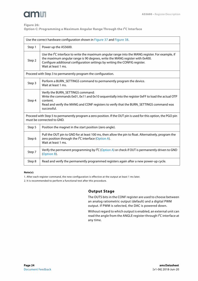
Figure 26:Option C: Programming a Maximum Angular Range Through the I²C Interface
Note(s):
1. After each register command, the new configuration is effective at the output at least 1 ms later.
2. It is recommended to perform a functional test after this procedure.
Output StageThe OUTS bits in the CONF register are used to choose between an analog ratiometric output (default) and a digital PWM output. If PWM is selected, the DAC is powered down.
Without regard to which output is enabled, an external unit can read the angle from the ANGLE register through I²C interface at any time.
Use the correct hardware configuration shown in Figure 37 and Figure 38.
Step 1 Power up the AS5600.
Step 2
Use the I²C interface to write the maximum angular range into the MANG register. For example, if the maximum angular range is 90 degrees, write the MANG register with 0x400.Configure additional configuration settings by writing the CONFIG register.Wait at least 1 ms.
Proceed with Step 3 to permanently program the configuration.
Step 3Perform a BURN_SETTINGS command to permanently program the device.Wait at least 1 ms.
Step 4
Verify the BURN_SETTINGS command: Write the commands 0x01, 0x11 and 0x10 sequentially into the register 0xFF to load the actual OTP content.Read and verify the MANG and CONF registers to verify that the BURN_SETTINGS command was successful.
Proceed with Step 5 to permanently program a zero position. If the OUT pin is used for this option, the PGO pin must be connected to GND.
Step 5 Position the magnet in the start position (zero angle).
Step 6Pull the OUT pin to GND for at least 100 ms, then allow the pin to float. Alternatively, program the zero position through the I²C interface (Option A).Wait at least 1 ms.
Step 7Verify the permanent programming by I²C (Option A) or check if OUT is permanently driven to GND (Option B).
Step 8 Read and verify the permanently programmed registers again after a new power-up cycle.
Page 24 ams Datasheet Document Feedback [v1-06] 2018-Jun-20
AS5600 − Register Description
Analog Output ModeBy default, the AS5600 output stage is configured as analog ratiometric output. The Digital to Analog Converter (DAC) has 12-bit resolution. In default mode, the lower reference voltage for the DAC is GND, while the upper reference voltage is VDD. The output voltage on the OUT pin is ratiometric between GND and VDD.
The maximum angular range can be programmed from 18 degrees to 360 degrees. The default range is 360 degrees.
As shown below, if the range is 360 degrees, to avoid discontinuity points exactly at the limit of the range, a 10-LSB hysteresis is applied. This hysteresis suppresses toggling the OUT pin when the magnet is close to zero or 360 degrees.
Figure 27:Output Characteristic Over a 360° Full-Turn Revolution
The AS5600 supports programming both a zero angle as well as the maximum angular range. As shown in Figure 28, reducing the maximum angular range pushes the non-discontinuity points to the edges, away from the 0 and θmax (where θmax is the maximum angle) by λ, where λ= (360 - θmax)/2.
Outp
ut V
olta
ge A
OUT[
V]
VDD
Angle (DEG)0 DEG 360 DEG
10LSB
10LSB
ams Datasheet Page 25[v1-06] 2018-Jun-20 Document Feedback
AS5600 − Register Description
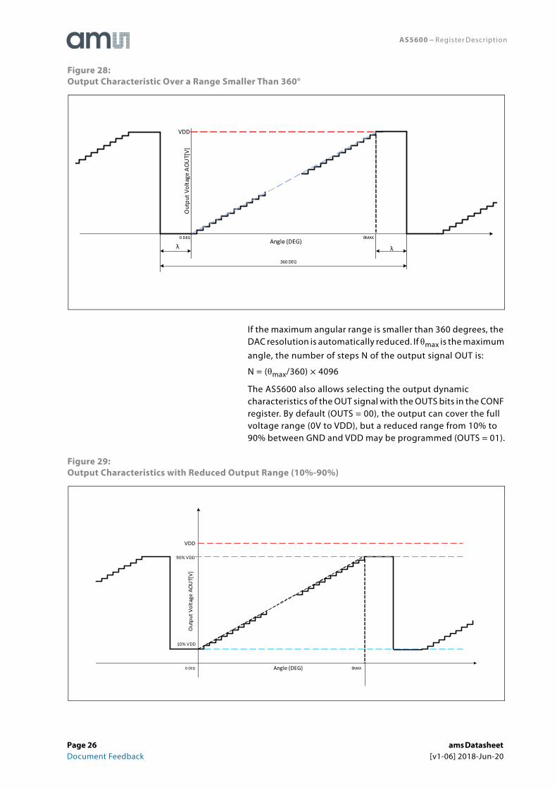
Figure 28:Output Characteristic Over a Range Smaller Than 360°
If the maximum angular range is smaller than 360 degrees, the DAC resolution is automatically reduced. If θmax is the maximum angle, the number of steps N of the output signal OUT is:
N = (θmax/360) × 4096
The AS5600 also allows selecting the output dynamic characteristics of the OUT signal with the OUTS bits in the CONF register. By default (OUTS = 00), the output can cover the full voltage range (0V to VDD), but a reduced range from 10% to 90% between GND and VDD may be programmed (OUTS = 01).
Figure 29:Output Characteristics with Reduced Output Range (10%-90%)
Out
put V
olta
ge A
OUT[
V]
VDD
Angle (DEG)0 DEG θMAX
λ λ
360 DEG
Out
put V
olta
ge A
OUT[
V]
VDD
Angle (DEG)0 DEG θMAX
90% VDD
10% VDD
Page 26 ams Datasheet Document Feedback [v1-06] 2018-Jun-20
AS5600 − Register Description
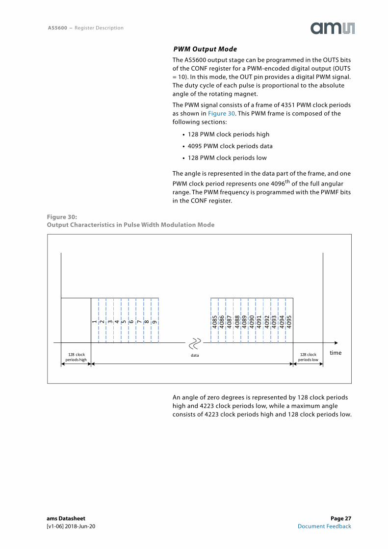
PWM Output ModeThe AS5600 output stage can be programmed in the OUTS bits of the CONF register for a PWM-encoded digital output (OUTS = 10). In this mode, the OUT pin provides a digital PWM signal. The duty cycle of each pulse is proportional to the absolute angle of the rotating magnet.
The PWM signal consists of a frame of 4351 PWM clock periods as shown in Figure 30. This PWM frame is composed of the following sections:
• 128 PWM clock periods high
• 4095 PWM clock periods data
• 128 PWM clock periods low
The angle is represented in the data part of the frame, and one
PWM clock period represents one 4096th of the full angular range. The PWM frequency is programmed with the PWMF bits in the CONF register.
Figure 30:Output Characteristics in Pulse Width Modulation Mode
An angle of zero degrees is represented by 128 clock periods high and 4223 clock periods low, while a maximum angle consists of 4223 clock periods high and 128 clock periods low.
time
1 2 3 4 5 6 7 8
4095
4094
4093
4092
4091
4090
4089
4088
4087
4086
4085
data 128 clock periods low
128 clock periods high
9
ams Datasheet Page 27[v1-06] 2018-Jun-20 Document Feedback
AS5600 − Register Description
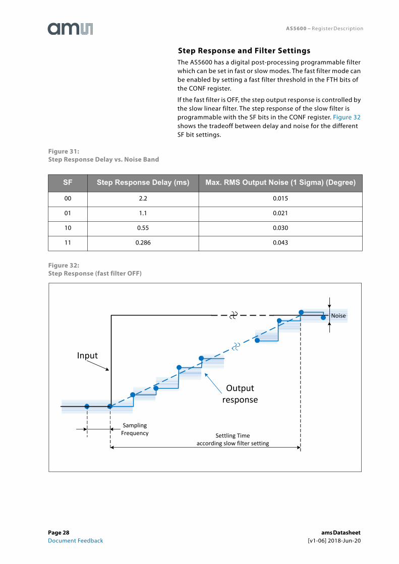
Step Response and Filter SettingsThe AS5600 has a digital post-processing programmable filter which can be set in fast or slow modes. The fast filter mode can be enabled by setting a fast filter threshold in the FTH bits of the CONF register.
If the fast filter is OFF, the step output response is controlled by the slow linear filter. The step response of the slow filter is programmable with the SF bits in the CONF register. Figure 32 shows the tradeoff between delay and noise for the different SF bit settings.
Figure 31:Step Response Delay vs. Noise Band
Figure 32:Step Response (fast filter OFF)
SF Step Response Delay (ms) Max. RMS Output Noise (1 Sigma) (Degree)
00 2.2 0.015
01 1.1 0.021
10 0.55 0.030
11 0.286 0.043
Input
Output response
Sampling Frequency Settling Time
according slow filter setting
Noise
Page 28 ams Datasheet Document Feedback [v1-06] 2018-Jun-20
AS5600 − Register Description
For a fast step response and low noise after settling, the fast filter can be enabled. The fast filter works only if the input variation is greater than the fast filter threshold, otherwise the output response is determined only by the slow filter. The fast filter threshold is programmed with the FTH bits in the CONF Register. As shown in Figure 34, the step response stays within an error band after two full sampling periods to settle to the final value determined by the slow filter.
Figure 33:Fast Filter Threshold
FTH Fast Filter Threshold (LSB)
Slow-to-fast filter Fast-to-slow filter
000 Slow filter only
001 6 1
010 7 1
011 9 1
100 18 2
101 21 2
110 24 2
111 10 4
ams Datasheet Page 29[v1-06] 2018-Jun-20 Document Feedback
AS5600 − Register Description
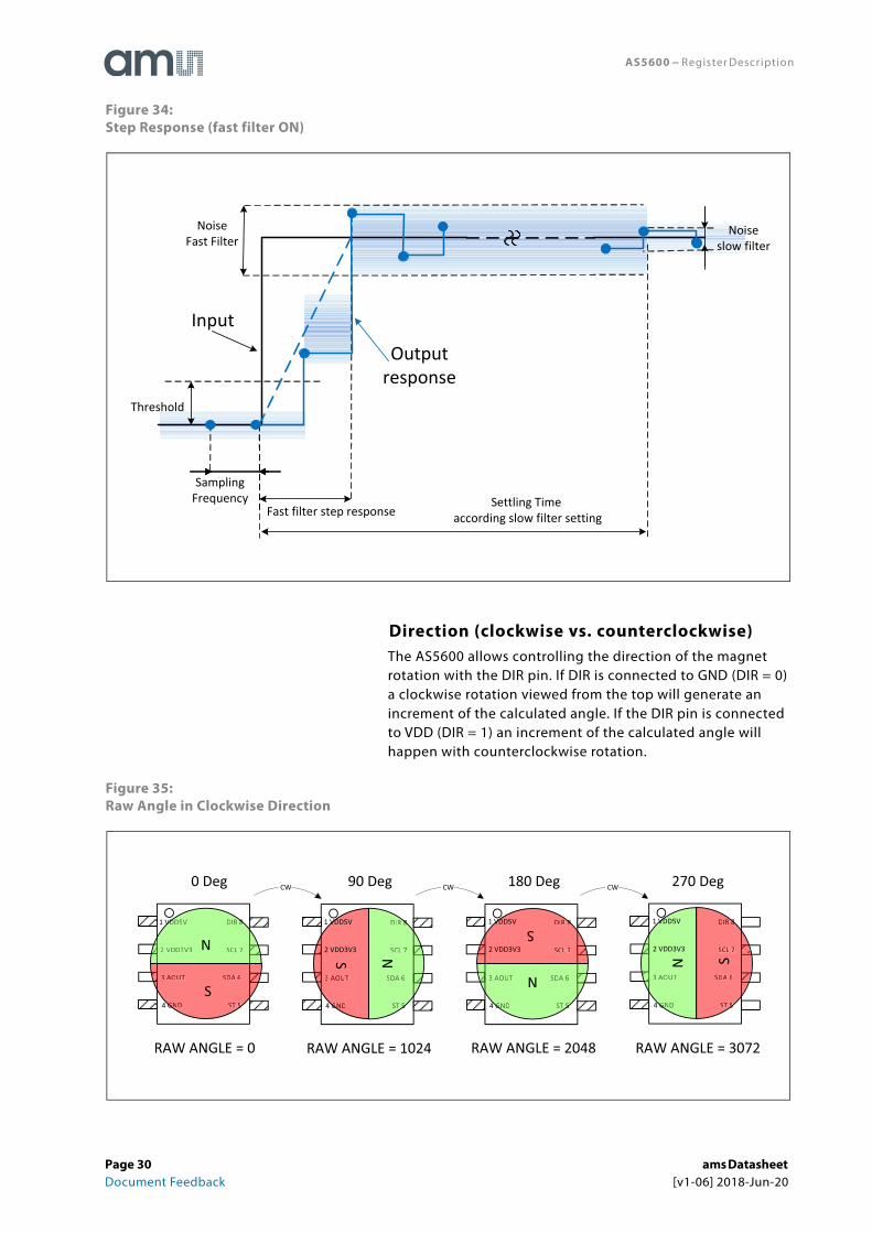
Figure 34:Step Response (fast filter ON)
Direction (clockwise vs. counterclockwise)The AS5600 allows controlling the direction of the magnet rotation with the DIR pin. If DIR is connected to GND (DIR = 0) a clockwise rotation viewed from the top will generate an increment of the calculated angle. If the DIR pin is connected to VDD (DIR = 1) an increment of the calculated angle will happen with counterclockwise rotation.
Figure 35:Raw Angle in Clockwise Direction
Input
Sampling Frequency Settling Time
according slow filter setting
NoiseFast Filter
Noiseslow filter
Output response
Fast filter step response
Threshold
1 VDD5V
2 VDD3V3
3 AOUT
4 GND
DIR 8
SCL 7
SDA 6
ST 5
3 AOUT
4 GND
DIR 8
SCL 7
SDA 6
ST 5
DIR 8
SCL 7
SDA 6
ST 5
3 AOUT
GND
NS
VDD5V
2 VDD3V3
DIR 8
SCL 7
3 AOUT
GND
SDA 6
ST 5
N
S3 AOUT
4 GND
DIR 8
SCL 7
SDA 6
ST 5
3 AOUT
4 GND
DIR 8
SCL 7
SDA 6
ST 5
3 AOUT
GND
DIR 8
SCL 7
SDA 6
ST 5
N S
3 AOUT
GND
SDA 6
ST 5
DIR 8
SCL 7
N
S
0 Deg 180 Deg90 Deg 270 Deg CW CW CW
RAW ANGLE = 0 RAW ANGLE = 1024 RAW ANGLE = 2048 RAW ANGLE = 3072
1 VDD5V
2 VDD3V3
1 VDD5V
2 VDD3V3
1 VDD5V
2 VDD3V3
Page 30 ams Datasheet Document Feedback [v1-06] 2018-Jun-20
AS5600 − Register Description
HysteresisTo avoid any toggling of the output when the magnet is not moving, a 1 to 3 LSB hysteresis of the 12-bit resolution can be enabled with the HYST bits in the CONF register.
Magnet DetectionAs a safety and diagnostic feature, the AS5600 indicates the absence of the magnet. If the measured magnet field strength goes below the minimum specified level (Bz_ERROR), the output is driven low, without regard to which output mode has been selected (analog or PWM) and the MD bit in the STATUS register is 0.
Low Power ModesA digital state machine automatically manages the low power modes to reduce the average current consumption. Three low power modes are available and can be enabled with the PM bits in the CONF register. Current consumption and polling times are shown in Figure 6.
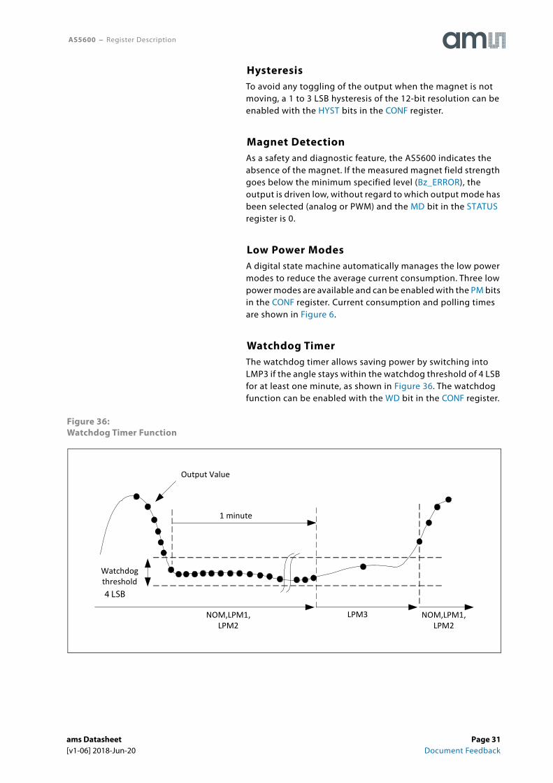
Watchdog TimerThe watchdog timer allows saving power by switching into LMP3 if the angle stays within the watchdog threshold of 4 LSB for at least one minute, as shown in Figure 36. The watchdog function can be enabled with the WD bit in the CONF register.
Figure 36:Watchdog Timer Function
1 minute
Watchdog threshold
LPM3 NOM,LPM1, LPM2
NOM,LPM1, LPM2
Output Value
4 LSB
ams Datasheet Page 31[v1-06] 2018-Jun-20 Document Feedback
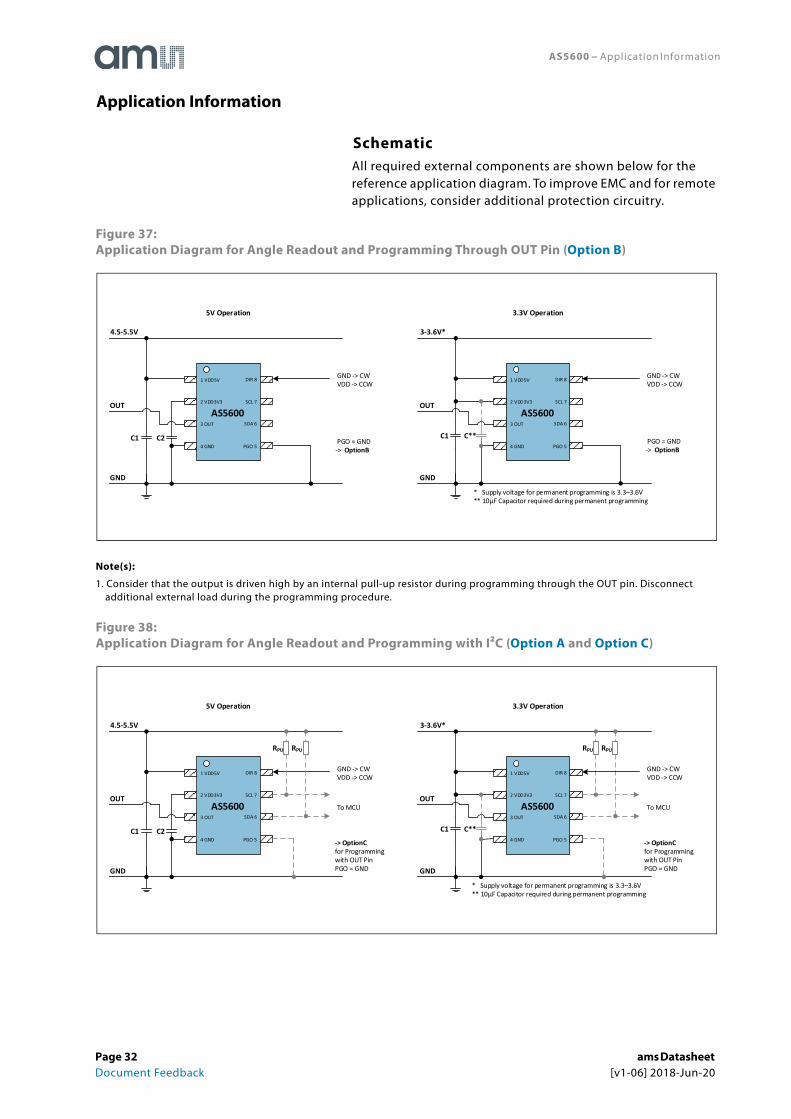
AS5600 − Application Information
SchematicAll required external components are shown below for the reference application diagram. To improve EMC and for remote applications, consider additional protection circuitry.
Figure 37:Application Diagram for Angle Readout and Programming Through OUT Pin (Option B)
Note(s):
1. Consider that the output is driven high by an internal pull-up resistor during programming through the OUT pin. Disconnect additional external load during the programming procedure.
Figure 38:Application Diagram for Angle Readout and Programming with I²C (Option A and Option C)
Application Information
GND -> CWVDD -> CCW
PGO = GND-> OptionB
4.5-5.5V
GND
AS5600
1 VDD5V
2 VDD3V3
3 OUT
4 GND
DIR 8
SCL 7
SDA 6
PGO 5
OUT
C1 C2
5V Operation
3-3.6V*
3.3V Operation
GND -> CWVDD -> CCW
GND
AS5600
1 VDD5V
2 VDD3V3
3 OUT
4 GND
DIR 8
SCL 7
SDA 6
PGO 5
OUT
C1 C**
* Supply voltage for permanent programming is 3.3–3.6V ** 10μF Capacitor required during permanent programming
PGO = GND-> OptionB
GND -> CWVDD -> CCW
To MCU
4.5-5.5V
GND
AS5600
1 VDD5V
2 VDD3V3
3 OUT
4 GND
DIR 8
SCL 7
SDA 6
PGO 5
OUT
RPURPU
C1 C2
5V Operation
3-3.6V*
3.3V Operation
GND -> CWVDD -> CCW
To MCU
GND
AS5600
1 VDD5V
2 VDD3V3
3 OUT
4 GND
DIR 8
SCL 7
SDA 6
PGO 5
OUT
RPURPU
C1 C**
* Supply voltage for permanent programming is 3.3–3.6V ** 10μF Capacitor required during permanent programming
-> OptionCfor Programming with OUT PinPGO = GND
-> OptionCfor Programming with OUT PinPGO = GND
Page 32 ams Datasheet Document Feedback [v1-06] 2018-Jun-20
AS5600 − Application Information
Figure 39:Recommended External Components
Note(s):
1. Given parameter characteristics have to be fulfilled over operation temperature and product lifetime
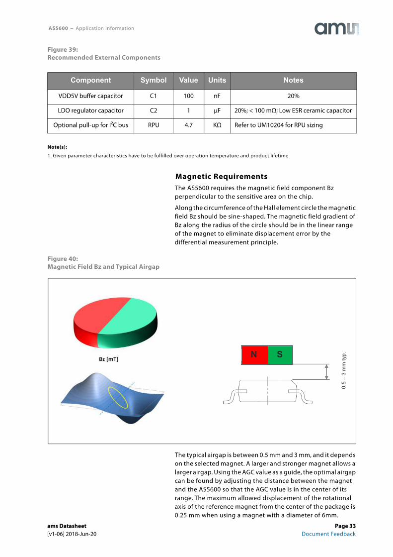
Magnetic RequirementsThe AS5600 requires the magnetic field component Bz perpendicular to the sensitive area on the chip.
Along the circumference of the Hall element circle the magnetic field Bz should be sine-shaped. The magnetic field gradient of Bz along the radius of the circle should be in the linear range of the magnet to eliminate displacement error by the differential measurement principle.
Figure 40:Magnetic Field Bz and Typical Airgap
The typical airgap is between 0.5 mm and 3 mm, and it depends on the selected magnet. A larger and stronger magnet allows a larger airgap. Using the AGC value as a guide, the optimal airgap can be found by adjusting the distance between the magnet and the AS5600 so that the AGC value is in the center of its range. The maximum allowed displacement of the rotational axis of the reference magnet from the center of the package is 0.25 mm when using a magnet with a diameter of 6mm.
Component Symbol Value Units Notes
VDD5V buffer capacitor C1 100 nF 20%
LDO regulator capacitor C2 1 μF 20%; < 100 mΩ; Low ESR ceramic capacitor
Optional pull-up for I²C bus RPU 4.7 KΩ Refer to UM10204 for RPU sizing
0.5 –
3 m
m ty
p. S N
ams Datasheet Page 33[v1-06] 2018-Jun-20 Document Feedback
AS5600 − Application Information
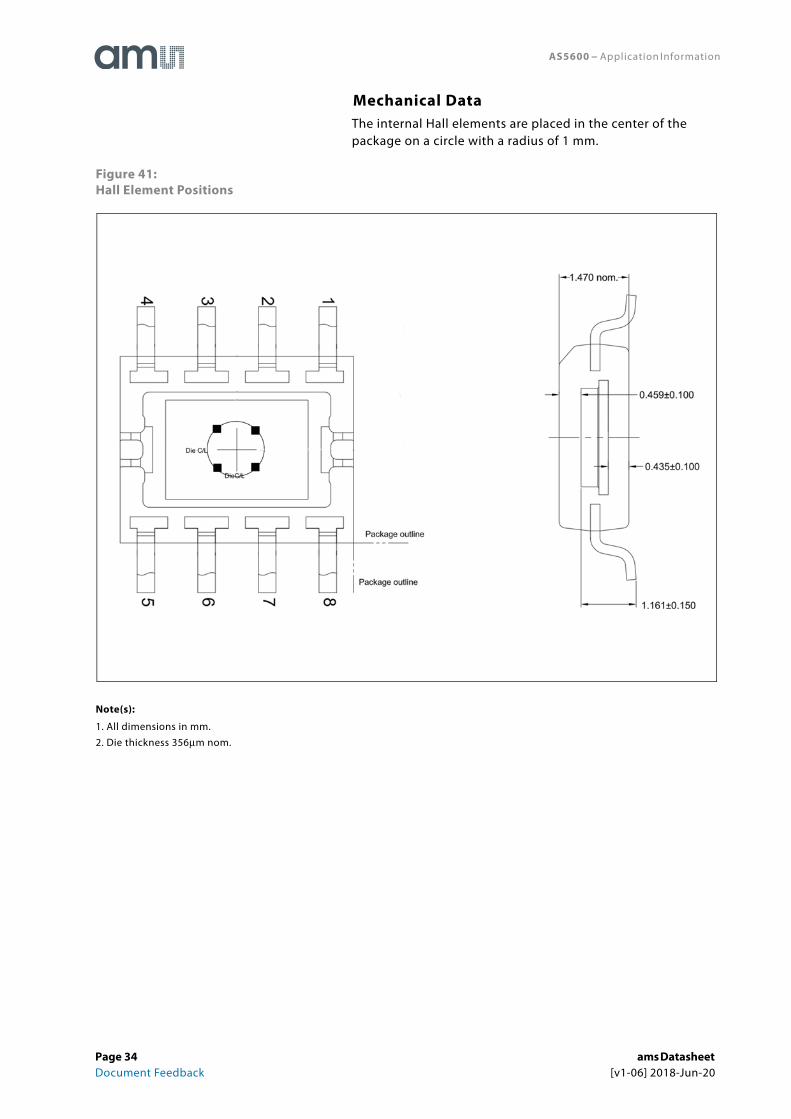
Mechanical DataThe internal Hall elements are placed in the center of the package on a circle with a radius of 1 mm.
Figure 41:Hall Element Positions
Note(s):
1. All dimensions in mm.
2. Die thickness 356μm nom.
Page 34 ams Datasheet Document Feedback [v1-06] 2018-Jun-20
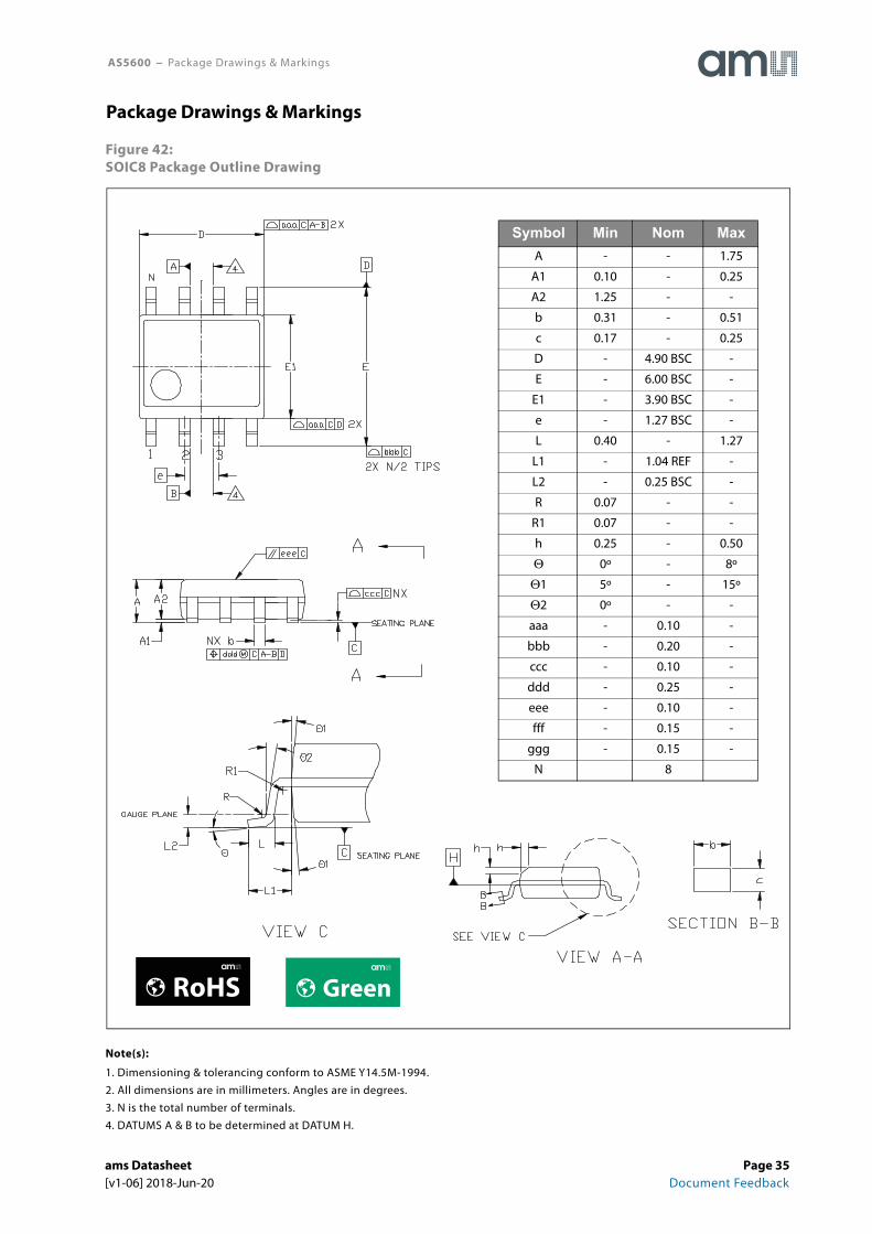
AS5600 − Package Drawings & Markings
Figure 42:SOIC8 Package Outline Drawing
Note(s):
1. Dimensioning & tolerancing conform to ASME Y14.5M-1994.
2. All dimensions are in millimeters. Angles are in degrees.
3. N is the total number of terminals.
4. DATUMS A & B to be determined at DATUM H.
Package Drawings & Markings
Symbol Min Nom MaxA - - 1.75
A1 0.10 - 0.25
A2 1.25 - -
b 0.31 - 0.51
c 0.17 - 0.25
D - 4.90 BSC -
E - 6.00 BSC -
E1 - 3.90 BSC -
e - 1.27 BSC -
L 0.40 - 1.27
L1 - 1.04 REF -
L2 - 0.25 BSC -
R 0.07 - -
R1 0.07 - -
h 0.25 - 0.50
Θ 0º - 8º
Θ1 5º - 15º
Θ2 0º - -
aaa - 0.10 -
bbb - 0.20 -
ccc - 0.10 -
ddd - 0.25 -
eee - 0.10 -
fff - 0.15 -
ggg - 0.15 -
N 8
GreenRoHS
ams Datasheet Page 35[v1-06] 2018-Jun-20 Document Feedback
AS5600 − Package Drawings & Mark ings
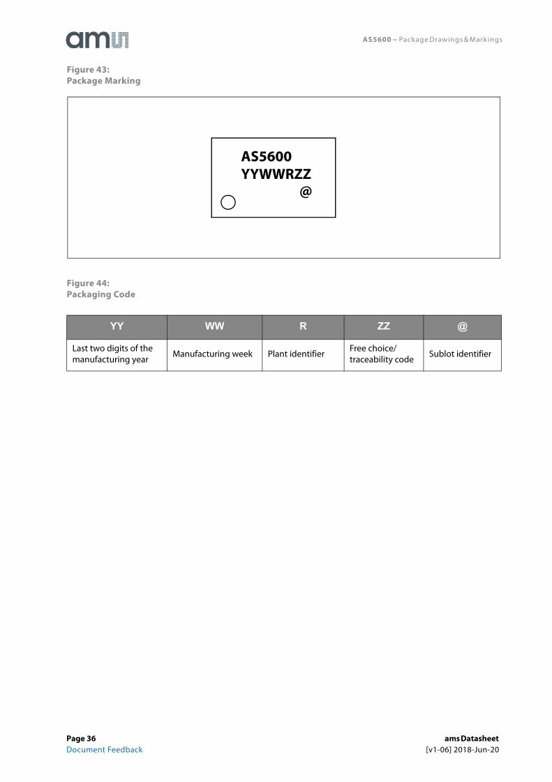
Figure 43:Package Marking
Figure 44:Packaging Code
YY WW R ZZ @
Last two digits of the manufacturing year
Manufacturing week Plant identifierFree choice/traceability code
Sublot identifier
AS5600YYWWRZZ
@
Page 36 ams Datasheet Document Feedback [v1-06] 2018-Jun-20
AS5600 − Ordering & Contact Information
Figure 45:Ordering Information
Buy our products or get free samples online at:www.ams.com/Products
Technical Support is available at:www.ams.com/Technical-Support
Provide feedback about this document at:www.ams.com/Document-Feedback
For further information and requests, e-mail us at:[email protected]
For sales offices, distributors and representatives, please visit: www.ams.com/Contact
Headquartersams AGTobelbader Strasse 308141 PremstaettenAustria, Europe
Tel: +43 (0) 3136 500 0
Website: www.ams.com
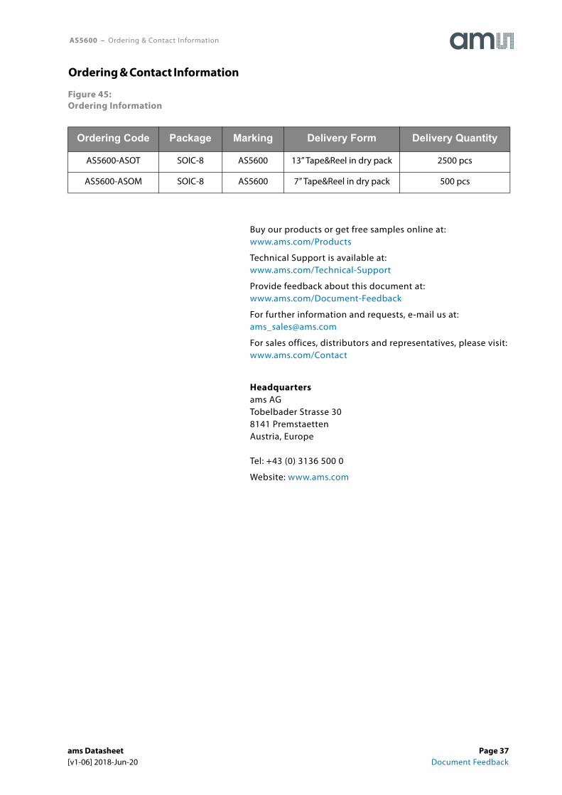
Ordering Code Package Marking Delivery Form Delivery Quantity
AS5600-ASOT SOIC-8 AS5600 13” Tape&Reel in dry pack 2500 pcs
AS5600-ASOM SOIC-8 AS5600 7” Tape&Reel in dry pack 500 pcs
Ordering & Contact Information
ams Datasheet Page 37[v1-06] 2018-Jun-20 Document Feedback
AS5600 − RoHS Compliant & ams Green Statement
RoHS: The term RoHS compliant means that ams AG products fully comply with current RoHS directives. Our semiconductor products do not contain any chemicals for all 6 substance categories, including the requirement that lead not exceed 0.1% by weight in homogeneous materials. Where designed to be soldered at high temperatures, RoHS compliant products are suitable for use in specified lead-free processes.
ams Green (RoHS compliant and no Sb/Br): ams Green defines that in addition to RoHS compliance, our products are free of Bromine (Br) and Antimony (Sb) based flame retardants (Br or Sb do not exceed 0.1% by weight in homogeneous material).
Important Information: The information provided in this statement represents ams AG knowledge and belief as of the date that it is provided. ams AG bases its knowledge and belief on information provided by third parties, and makes no representation or warranty as to the accuracy of such information. Efforts are underway to better integrate information from third parties. ams AG has taken and continues to take reasonable steps to provide representative and accurate information but may not have conducted destructive testing or chemical analysis on incoming materials and chemicals. ams AG and ams AG suppliers consider certain information to be proprietary, and thus CAS numbers and other limited information may not be available for release.
RoHS Compliant & ams Green Statement
Page 38 ams Datasheet Document Feedback [v1-06] 2018-Jun-20
AS5600 − Copyrights & Disclaimer
Copyright ams AG, Tobelbader Strasse 30, 8141 Premstaetten, Austria-Europe. Trademarks Registered. All rights reserved. The material herein may not be reproduced, adapted, merged, translated, stored, or used without the prior written consent of the copyright owner.
Devices sold by ams AG are covered by the warranty and patent indemnification provisions appearing in its General Terms of Trade. ams AG makes no warranty, express, statutory, implied, or by description regarding the information set forth herein. ams AG reserves the right to change specifications and prices at any time and without notice. Therefore, prior to designing this product into a system, it is necessary to check with ams AG for current information. This product is intended for use in commercial applications. Applications requiring extended temperature range, unusual environmental requirements, or high reliability applications, such as military, medical life-support or life-sustaining equipment are specifically not recommended without additional processing by ams AG for each application. This product is provided by ams AG “AS IS” and any express or implied warranties, including, but not limited to the implied warranties of merchantability and fitness for a particular purpose are disclaimed.
ams AG shall not be liable to recipient or any third party for any damages, including but not limited to personal injury, property damage, loss of profits, loss of use, interruption of business or indirect, special, incidental or consequential damages, of any kind, in connection with or arising out of the furnishing, performance or use of the technical data herein. No obligation or liability to recipient or any third party shall arise or flow out of ams AG rendering of technical or other services.
Copyrights & Disclaimer
ams Datasheet Page 39[v1-06] 2018-Jun-20 Document Feedback
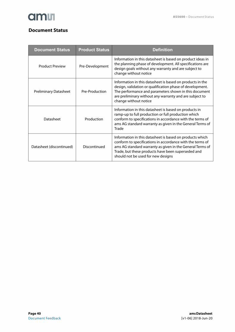
AS5600 − Document Status
Document Status Product Status Definition
Product Preview Pre-Development
Information in this datasheet is based on product ideas in the planning phase of development. All specifications are design goals without any warranty and are subject to change without notice
Preliminary Datasheet Pre-Production
Information in this datasheet is based on products in the design, validation or qualification phase of development. The performance and parameters shown in this document are preliminary without any warranty and are subject to change without notice
Datasheet Production
Information in this datasheet is based on products in ramp-up to full production or full production which conform to specifications in accordance with the terms of ams AG standard warranty as given in the General Terms of Trade
Datasheet (discontinued) Discontinued
Information in this datasheet is based on products which conform to specifications in accordance with the terms of ams AG standard warranty as given in the General Terms of Trade, but these products have been superseded and should not be used for new designs
Document Status
Page 40 ams Datasheet Document Feedback [v1-06] 2018-Jun-20
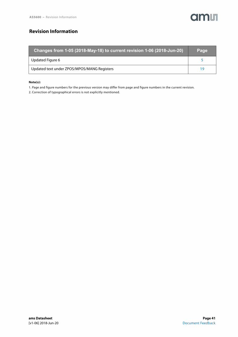
AS5600 − Revision Information
Note(s):
1. Page and figure numbers for the previous version may differ from page and figure numbers in the current revision.
2. Correction of typographical errors is not explicitly mentioned.
Changes from 1-05 (2018-May-18) to current revision 1-06 (2018-Jun-20) Page
Updated Figure 6 5
Updated text under ZPOS/MPOS/MANG Registers 19
Revision Information
ams Datasheet Page 41[v1-06] 2018-Jun-20 Document Feedback
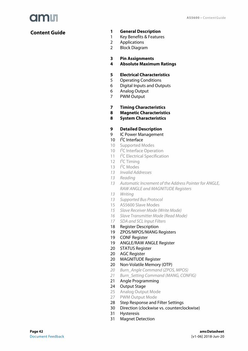
AS5600 − Content Guide
1 General Description1 Key Benefits & Features2 Applications 2 Block Diagram
3 Pin Assignments4 Absolute Maximum Ratings
5 Electrical Characteristics5 Operating Conditions6 Digital Inputs and Outputs6 Analog Output7 PWM Output
7 Timing Characteristics8 Magnetic Characteristics8 System Characteristics
9 Detailed Description9 IC Power Management10 I²C Interface10 Supported Modes10 I²C Interface Operation11 I²C Electrical Specification12 I²C Timing13 I²C Modes13 Invalid Addresses13 Reading13 Automatic Increment of the Address Pointer for ANGLE,
RAW ANGLE and MAGNITUDE Registers13 Writing13 Supported Bus Protocol15 AS5600 Slave Modes15 Slave Receiver Mode (Write Mode)16 Slave Transmitter Mode (Read Mode)17 SDA and SCL Input Filters 18 Register Description19 ZPOS/MPOS/MANG Registers19 CONF Register19 ANGLE/RAW ANGLE Register20 STATUS Register20 AGC Register20 MAGNITUDE Register20 Non-Volatile Memory (OTP)20 Burn_Angle Command (ZPOS, MPOS)21 Burn_Setting Command (MANG, CONFIG)21 Angle Programming24 Output Stage25 Analog Output Mode27 PWM Output Mode28 Step Response and Filter Settings30 Direction (clockwise vs. counterclockwise)31 Hysteresis31 Magnet Detection
Content Guide
Page 42 ams Datasheet Document Feedback [v1-06] 2018-Jun-20
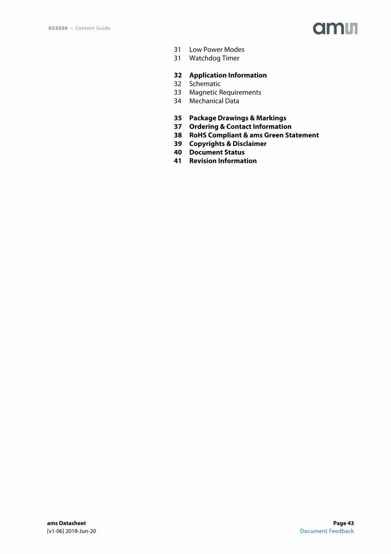
AS5600 − Content Guide
31 Low Power Modes31 Watchdog Timer
32 Application Information32 Schematic33 Magnetic Requirements34 Mechanical Data
35 Package Drawings & Markings37 Ordering & Contact Information38 RoHS Compliant & ams Green Statement39 Copyrights & Disclaimer40 Document Status41 Revision Information
ams Datasheet Page 43[v1-06] 2018-Jun-20 Document Feedback


![New AS5600 · 2020. 5. 21. · Page 2 ams Datasheet Document Feedback [v1-06] 2018-Jun-20 AS5600 − General Description Applications The AS5600 is ideally suited for contactless](https://img.pdfslide.us/doc/110x75/6072ab7b0a3ad342c51e1563/new-as5600-2020-5-21-page-2-ams-datasheet-document-feedback-v1-06-2018-jun-20.jpg)