Embed Size (px)
Citation preview
Product
Folder
Order
Now
Technical
Documents
Tools &
Software
Support &Community
An IMPORTANT NOTICE at the end of this data sheet addresses availability, warranty, changes, use in safety-critical applications,intellectual property matters and other important disclaimers. PRODUCTION DATA.
TPS659121, TPS659122SWCS071C –AUGUST 2012–REVISED AUGUST 2017
TPS65912x PMU for Processor Power
1 Device Overview
1
1.1 Features1
• Four Step-Down Converters:– VIN Range From 2.7 V to 5.5 V– Power Save Mode at Light Load Current– Output Voltage Accuracy in PWM Mode ±2%– Typical 26-μA Quiescent Current per Converter– Dynamic Voltage Scaling– 100% Duty Cycle for Lowest Dropout
• Ten LDOs:– 8 General-Purpose LDOs– Output Voltage Range From 0.8 V to 3.3 V– 2 Low-Noise RF-LDOs– Output Voltage Range From 1.6 V to 3.3 V– 32-μA Quiescent Current– Preregulation Support by Separate Power
Inputs– ECO Mode– VIN Range of LDOs Respective to the Following
Voltage Ranges:– 1.8 V to 3.6 V– 3.0 V to 5.5 V
• Three LED Outputs:
– Internal Dimming Using I2C– Multiplexed With GPIOs– Up to 20 mA per Current Sink
• Thermal Monitoring– High Temperature Warning– Thermal Shutdown
• Bypass Switch– Used With DCDC4 in Applications Powering an
RF-PA– For Example, as Supply Switch for SD Cards
• Interface– I2C Interface– Power I2C Interface for Dynamic Voltage
Scaling– SPI
• 32-kHz RC Oscillator• Undervoltage Lockout and Battery Fault
Comparator• Long Button-Press Detection• Flexible Power-Up and Power-Down Sequencing• 3.6-mm × 3.6-mm DSBGA Package With 0.4-mm
Pitch
1.2 Applications• Data Cards• Smart Phones• Wireless Routers and Switches• Tablets
• Industrial Applications• LTE Modem• GPS
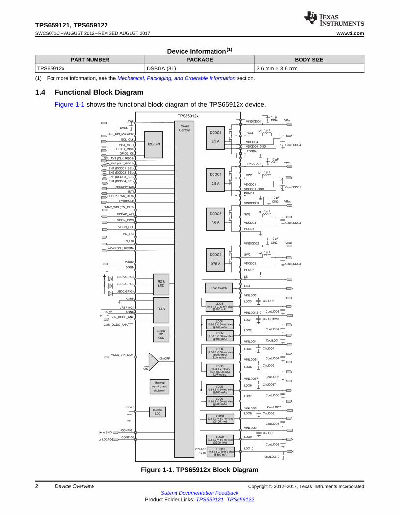
1.3 DescriptionThe TPS65912x device provides four configurable step-down converters with up to 2.5-A output currentfor memory, processor core, I/O, or preregulation of LDOs. The device also contains ten LDO regulatorsfor external use. These LDOs can be supplied from either a battery or a preregulated supply. Power-up orpower-down controller is configurable and can support any power-up or power-down sequences(OTP-based). The TPS65912x device integrates a 32-kHz RC oscillator to sequence all resources duringpower up or power down. All LDOs and DC-DC converters can be controlled by I2C-SPI interface or basicENABLE balls. In addition, an independent automatic voltage-scaling interface allows for transitioningDC-DC to a different voltage by I2C or basic Roof/Floor Control. Three RGB LEDs with an advanceddimming feature are integrated inside the device. GPIO functionality is multiplexed with LED/ENABLE/SPIwhen not used. Each GPIO can be configured as part of the power-up sequence to control externalresources. One SLEEP pin enables power mode control between active mode and preprogrammed sleepmode for power optimization. For system control, the TPS65912x device has one comparator for systemstate management. The TPS65912x device comes in a 9-pin × 9-pin DSBGA package (3.6 mm × 3.6 mm)with a 0.4-mm pitch.
VBat
VBat
VBat
SDA_MOSI
SCL_CLK
VINLDO3
LDO3
VDDIO
SW4DCDC4
2.5 A VDCDC4
VINDCDC4
AGND
VREF1V25
PGND4
SW3
VDCDC3
PGND3
SW2
VINDCDC2
10 µF
PGND2
GPIO2_CE
GPIO1_MISO
I2C/SPI
nPWRON (nRESIN)
nRESPWRON
INT1
SLEEP (PWR_REQ)
PWRHOLD
DGND
VINLDO1210
LDO1LDO1
(0.8-3.3 V, 50 mV step
@100 mA)LDO2
LDO2(0.8-3.3 V, 50 mV step
@100 mA)VINLDO4
LDO4LDO4(1.6-3.3 V, 50 mV step
@250 mA)Low noise
LDO5
LDO6
VINLDO5
LDO7LDO7
(0.8-3.3 V, 50 mV step@200 mA)
LDO8
LDO9LDO9(0.8-3.3 V, 50 mV step
@300 mA)
RGBLED
BIAS
PowerControl
TPS65912x
32 kHzRC
OSC
ON/OFF
Vth
+
-
SDA_AVS (CLK_REQ2)
SCL_AVS (CLK_REQ1)
EN1 (DCDC1_SEL)
EN2 (DCDC2_SEL)
VINLDO67
LDO5(1.6-3.3 V, 50 mV
step @250 mA)Low noise
LDO6(0.8-3.3 V, 50 mV step
@100 mA)
LDO3(0.8-3.3 V, 50 mV step
@100 mA)
LDO8(0.8-3.3 V, 50 mV step
@100 mA)
EN3 (DCDC3_SEL)
EN4 (DCDC4_SEL)
Thermal
warning and
shutdown
LDOAOInternal
LDO
LEDA/GPIO3
LEDB/GPIO4
LEDC/GPIO5
LDO10LDO10(0.8-3.3 V, 50 mV step
@300 mA)
VINLDO
1210
Load Switch
LSI
LSO
L4
L3
L2
CoutDCDC4
CoutDCDC3
CoutDCDC3
CIN4
CIN3
CIN2
VDCDC4_GND
VBat
SW1
VDCDC1
VINDCDC1
PGND1
L1
CoutDCDC1
CIN1
VDCDC1_GND
VINDCDC3
VDCDC2
CoutLDO3
CoutLDO2
CoutLDO1
CoutLDO4
CoutLDO5
CoutLDO6
CoutLDO7
CoutLDO8
CoutLDO9
CoutLDO10
CinLDO67
CinLDO5
CinLDO4
CinLDO1210
CinLDO3
VINLDO8
CinLDO8
VINLDO9
CinLDO9
VCON_PWM
VCON_CLK
OMAP_WDI (32k_OUT)
CONFIG1
CONFIG2
VIN_DCDC_ANA
DEF_SPI_I2C-GPIO
VCC
CPCAP_WDI
AGND
EN_LS0
EN_LS1
CVIN_DCDC_ANA
CVCC
VCCS_VIN_MON
tie to GND
or LDOAO
10 µF
1 µH
1 µH
10 µF
10 µF
1 µH
1 µH
DCDC1
2.5 A
DCDC3
1.6 A
DCDC2
0.75 A
100 nF
2
TPS659121, TPS659122SWCS071C –AUGUST 2012–REVISED AUGUST 2017 www.ti.com
Submit Documentation FeedbackProduct Folder Links: TPS659121 TPS659122
Device Overview Copyright © 2012–2017, Texas Instruments Incorporated
(1) For more information, see the Mechanical, Packaging, and Orderable Information section.
Device Information (1)
PART NUMBER PACKAGE BODY SIZETPS65912x DSBGA (81) 3.6 mm × 3.6 mm
1.4 Functional Block DiagramFigure 1-1 shows the functional block diagram of the TPS65912x device.
Figure 1-1. TPS65912x Block Diagram
3
TPS659121, TPS659122www.ti.com SWCS071C –AUGUST 2012–REVISED AUGUST 2017
Submit Documentation FeedbackProduct Folder Links: TPS659121 TPS659122
Table of ContentsCopyright © 2012–2017, Texas Instruments Incorporated
Table of Contents1 Device Overview ......................................... 1
1.1 Features .............................................. 11.2 Applications........................................... 11.3 Description............................................ 11.4 Functional Block Diagram ............................ 2
2 Revision History ......................................... 43 Default Settings .......................................... 54 Pin Configuration and Functions..................... 6
4.1 Pin Functions ......................................... 75 Specifications ........................................... 10
5.1 Absolute Maximum Ratings ......................... 105.2 ESD Ratings ........................................ 105.3 Recommended Operating Conditions............... 115.4 Thermal Characteristics ............................. 125.5 Electrical Characteristics – DCDC1, DCDC2, and
DCDC3 .............................................. 125.6 Electrical Characteristics – DCDC4 ................. 145.7 Electrical Characteristics – LDOs ................... 155.8 Electrical Characteristics – Digital Inputs, Digital
Outputs ............................................. 175.9 Electrical Characteristics – VMON Voltage Monitor,
VDDIO, Undervoltage Lockout (UVLO), and LDOAO...................................................... 17
5.10 Electrical Characteristics – Load Switch ........... 185.11 Electrical Characteristics – LED Drivers ........... 185.12 Electrical Characteristics – Thermal Monitoring and
Shutdown ........................................... 185.13 Electrical Characteristics – 32-kHz RC Clock ...... 195.14 SPI Interface Timing Requirements................. 195.15 I2C Interface Timing Requirements ................ 195.16 Typical Characteristics .............................. 21
6 Parameter Measurement Information .............. 266.1 I2C Timing Diagrams ................................ 266.2 SPI Timing Diagram................................. 27
7 Detailed Description ................................... 287.1 Overview ........................................... 287.2 Functional Block Diagram........................... 297.3 Linear Regulators ................................... 307.4 Step-Down Converters .............................. 317.5 GPIOs ............................................... 327.6 Power State Machine ............................... 337.7 Transition Conditions................................ 33
7.8 Implementation of Internal Power-Up and Power-Down Sequencing................................... 41
7.9 EN1, EN2, EN3, EN4, Resources Control .......... 437.10 SLEEP State Control................................ 437.11 Registers SET_OFF, KEEP_ON and DEF_VOLT
Used in SLEEP State; CONFIG2 = 1 ............... 437.12 Registers SET_OFF, KEEP_ON and DEF_VOLT
Used for Resources Assigned to an External EnablePin; CONFIG2 = 1 .................................. 44
7.13 Registers SET_OFF, KEEP_ON and DEF_VOLT forResources Assigned to Pins PWR_REQ,CLK_REQ1 and CLK_REQ2; CONFIG2 = 0 ....... 44
7.14 Voltage Scaling Interface Control Using _OP and_AVS Registers with I2C or SPI Interface........... 44
7.15 Voltage Scaling Using the VCON Decoder on PinsVCON_PWM and VCON_CLK...................... 45
7.16 Configuration Pins CONFIG1, CONFIG2 andDEF_SPI_I2C-GPIO................................. 47
7.17 VDDIO Voltage for Push-Pull Output Stages ....... 487.18 Digital Signal Summary ............................. 487.19 TPS659121 On/Off Operation With E450, E500 .... 497.20 TPS659122 On/Off Operation for CONFIG1=HIGH 517.21 TPS659122 On/Off Operation for CONFIG1=LOW . 547.22 Interfaces............................................ 547.23 Serial Peripheral Interface .......................... 557.24 I2C Interface ........................................ 567.25 Thermal Monitoring and Shutdown ................. 597.26 Load Switch ......................................... 597.27 LED Driver .......................................... 617.28 Memory.............................................. 63
8 Applications, Implementation, and Layout ...... 1248.1 Application Information ............................ 1248.2 Typical Application ................................. 1258.3 Power Supply Recommendations ................. 135
9 Device and Documentation Support .............. 1369.1 Device Support..................................... 1369.2 Documentation Support............................ 1369.3 Receiving Notification of Documentation Updates. 1379.4 Community Resources............................. 1379.5 Trademarks ........................................ 1379.6 Electrostatic Discharge Caution ................... 1379.7 Glossary............................................ 137
10 Mechanical, Packaging, and OrderableInformation ............................................. 137
4
TPS659121, TPS659122SWCS071C –AUGUST 2012–REVISED AUGUST 2017 www.ti.com
Submit Documentation FeedbackProduct Folder Links: TPS659121 TPS659122
Revision History Copyright © 2012–2017, Texas Instruments Incorporated
2 Revision HistoryNOTE: Page numbers for previous revisions may differ from page numbers in the current version.
Changes from Revision B (April 2015) to Revision C Page
• Deleted the Ordering Information table ............................................................................................ 5• Changed the TPS659122 default output voltage setting for CONFIG1=LOW for DCDC1_OP / DCDC1_AVS,
DCDC3_OP / DCDC3_AVS, and DCDC4_OP / DCDC4_AVS in the Default Settings for TPS659122 table ............ 5• Changed some bit values for TPS659122 for CONFIG1=LOW and TPS659122 for CONFIG1=HIGH in the
ECEC and LDO register sections ................................................................................................. 63• Added the Application Information, Design Parameters, external component list, and Layout Example ............. 124• Added the Receiving Notification of Documentation Updates section ...................................................... 137
Changes from Revision A (March 2015) to Revision B Page
• Changed Applications section....................................................................................................... 1
Changes from Original (August 2012) to Revision A Page
• Changed format of the data sheet to TI standard ............................................................................... 1• Added TPS659122 part number ................................................................................................... 1
5
TPS659121, TPS659122www.ti.com SWCS071C –AUGUST 2012–REVISED AUGUST 2017
Submit Documentation FeedbackProduct Folder Links: TPS659121 TPS659122
Default SettingsCopyright © 2012–2017, Texas Instruments Incorporated
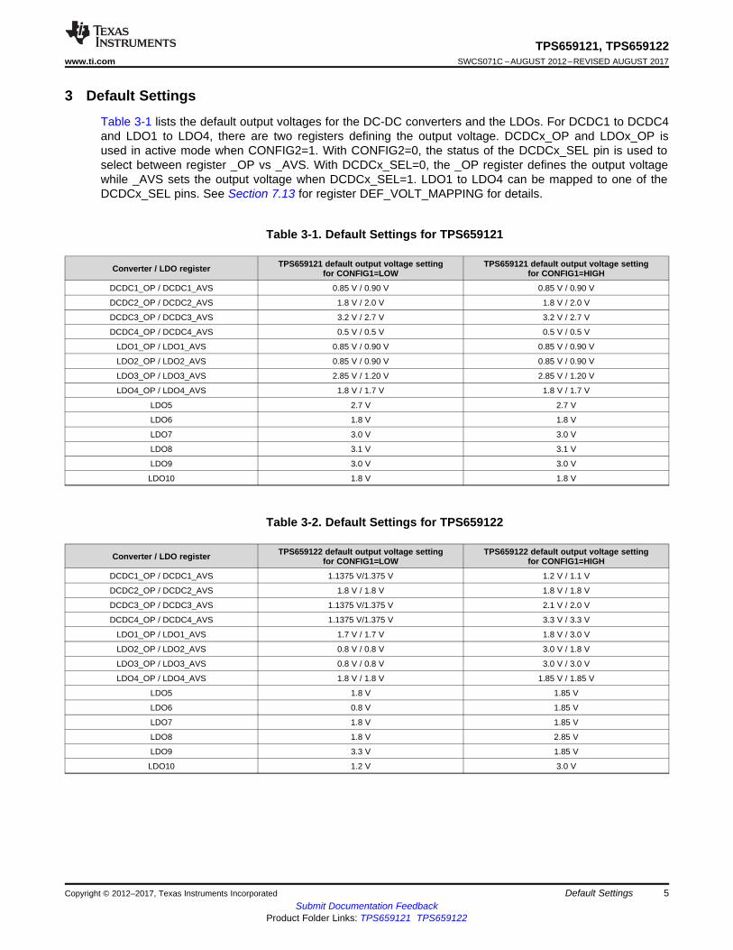
3 Default Settings
Table 3-1 lists the default output voltages for the DC-DC converters and the LDOs. For DCDC1 to DCDC4and LDO1 to LDO4, there are two registers defining the output voltage. DCDCx_OP and LDOx_OP isused in active mode when CONFIG2=1. With CONFIG2=0, the status of the DCDCx_SEL pin is used toselect between register _OP vs _AVS. With DCDCx_SEL=0, the _OP register defines the output voltagewhile _AVS sets the output voltage when DCDCx_SEL=1. LDO1 to LDO4 can be mapped to one of theDCDCx_SEL pins. See Section 7.13 for register DEF_VOLT_MAPPING for details.
Table 3-1. Default Settings for TPS659121
Converter / LDO register TPS659121 default output voltage settingfor CONFIG1=LOW
TPS659121 default output voltage settingfor CONFIG1=HIGH
DCDC1_OP / DCDC1_AVS 0.85 V / 0.90 V 0.85 V / 0.90 V
DCDC2_OP / DCDC2_AVS 1.8 V / 2.0 V 1.8 V / 2.0 V
DCDC3_OP / DCDC3_AVS 3.2 V / 2.7 V 3.2 V / 2.7 V
DCDC4_OP / DCDC4_AVS 0.5 V / 0.5 V 0.5 V / 0.5 V
LDO1_OP / LDO1_AVS 0.85 V / 0.90 V 0.85 V / 0.90 V
LDO2_OP / LDO2_AVS 0.85 V / 0.90 V 0.85 V / 0.90 V
LDO3_OP / LDO3_AVS 2.85 V / 1.20 V 2.85 V / 1.20 V
LDO4_OP / LDO4_AVS 1.8 V / 1.7 V 1.8 V / 1.7 V
LDO5 2.7 V 2.7 V
LDO6 1.8 V 1.8 V
LDO7 3.0 V 3.0 V
LDO8 3.1 V 3.1 V
LDO9 3.0 V 3.0 V
LDO10 1.8 V 1.8 V
Table 3-2. Default Settings for TPS659122
Converter / LDO register TPS659122 default output voltage settingfor CONFIG1=LOW
TPS659122 default output voltage settingfor CONFIG1=HIGH
DCDC1_OP / DCDC1_AVS 1.1375 V/1.375 V 1.2 V / 1.1 V
DCDC2_OP / DCDC2_AVS 1.8 V / 1.8 V 1.8 V / 1.8 V
DCDC3_OP / DCDC3_AVS 1.1375 V/1.375 V 2.1 V / 2.0 V
DCDC4_OP / DCDC4_AVS 1.1375 V/1.375 V 3.3 V / 3.3 V
LDO1_OP / LDO1_AVS 1.7 V / 1.7 V 1.8 V / 3.0 V
LDO2_OP / LDO2_AVS 0.8 V / 0.8 V 3.0 V / 1.8 V
LDO3_OP / LDO3_AVS 0.8 V / 0.8 V 3.0 V / 3.0 V
LDO4_OP / LDO4_AVS 1.8 V / 1.8 V 1.85 V / 1.85 V
LDO5 1.8 V 1.85 V
LDO6 0.8 V 1.85 V
LDO7 1.8 V 1.85 V
LDO8 1.8 V 2.85 V
LDO9 3.3 V 1.85 V
LDO10 1.2 V 3.0 V
VLDO7
A1A2 A3 A4
B1
C1
D1
VINLDO67 VLDO6 VDCDC4
VDCDC4_
GND
LEDC_
GPIO5
VINDCDC3 EN_LS1 EN_LS0 GPIO2_CE
SW3 CONFIG2 PWRONGPIO1
_MISO
PGND4
A5 A6 A7
SW4 VINDCDC4 LSO
LSIVINDCDC4SW4PGND4
EN4/
DCDC4
_SELAGND
VINDCDC
_ANA
SCL_CLKPWRHOLD
_ON VDCDC2
EN2 /
DCDC2
_SEL
VINDCDC2
SW2
LSI
PGND3
E1 E2 E3 E4
F1
G1
H1
CONFIG1 DGND SDA_MOSI
VCON
_PWMAGNDVDCDC3VINLDO4
VLDO4VCCS /
VIN_MON LDOAOSLEEP /
PWR_REQ
VLDO2 VCC VREF1V25VDCDC1
_GND
SCL_AVS
CLKREQ1
E5 E7 E8
SDA_AVS
CLKREQ2
DEF_SPI
_I2C
EN1 /
DCDC1
_SEL
VINLDO3VDDIO
OMAP
_WDI
/32kCLK
VCON
_CLK
INT1
nRES
PWRON/
VSUPOUT
CPCAP
_WDIVINLDO5
PGND1 SW1 VINDCDC1 VINLDO8
PGND2
VLDO5
VLDO8
VLDO3
J1
VLDO10VINLDO
1210VLDO1 VDCDC1 PGND1 SW1 VINDCDC1 VINLDO9 VLDO9
A8 A9
LSO
B2 B3 B4 B5 B6 B7 B8 B9
LEDB_
GPIO4
LEDA_
GPIO3
C2 C3 C4 C5 C6
EN3/
DCDC3
_SELC7 C8 C9
D2 D3 D4 D5 D6 D7 D8 D9
E6 E9
F2 F3 F4 F5 F6 F7 F8 F9
G2 G3 G4 G5 G6 G7 G8 G9
H2 H3 H4 H5 H6 H7 H8 H9
J9J8J7J6J5J4J3J2
6
TPS659121, TPS659122SWCS071C –AUGUST 2012–REVISED AUGUST 2017 www.ti.com
Submit Documentation FeedbackProduct Folder Links: TPS659121 TPS659122
Pin Configuration and Functions Copyright © 2012–2017, Texas Instruments Incorporated
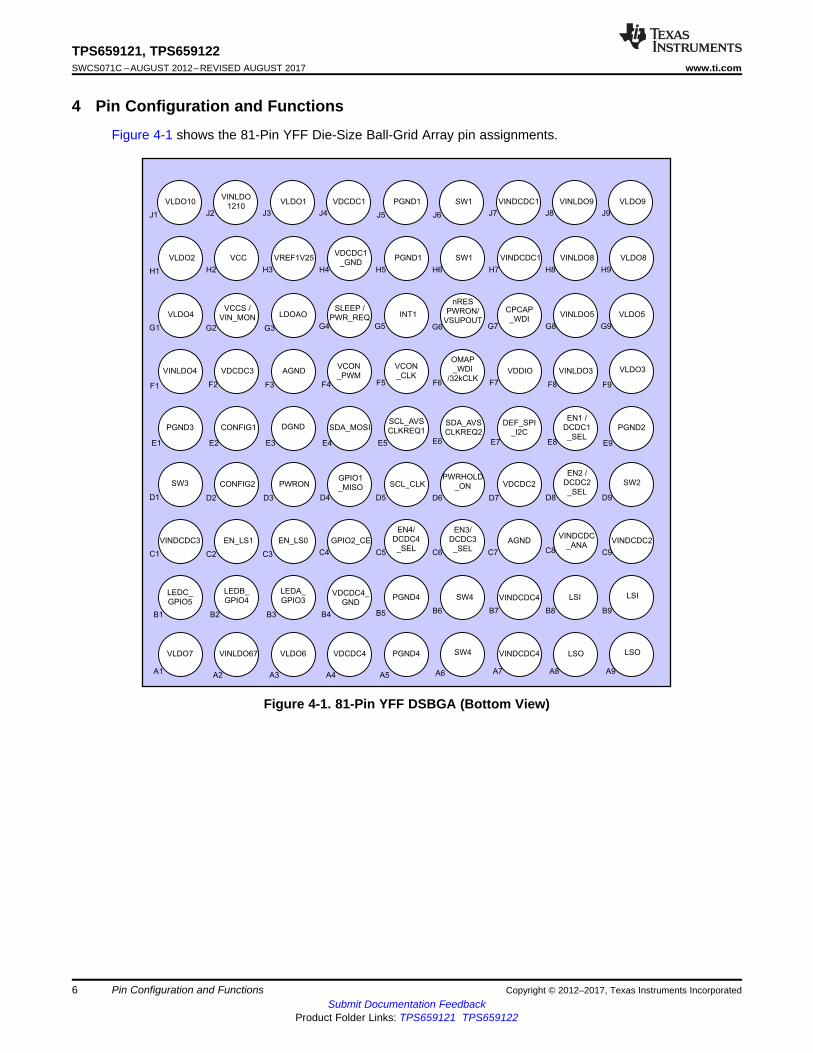
4 Pin Configuration and Functions
Figure 4-1 shows the 81-Pin YFF Die-Size Ball-Grid Array pin assignments.
Figure 4-1. 81-Pin YFF DSBGA (Bottom View)
7
TPS659121, TPS659122www.ti.com SWCS071C –AUGUST 2012–REVISED AUGUST 2017
Submit Documentation FeedbackProduct Folder Links: TPS659121 TPS659122
Pin Configuration and FunctionsCopyright © 2012–2017, Texas Instruments Incorporated
4.1 Pin Functions
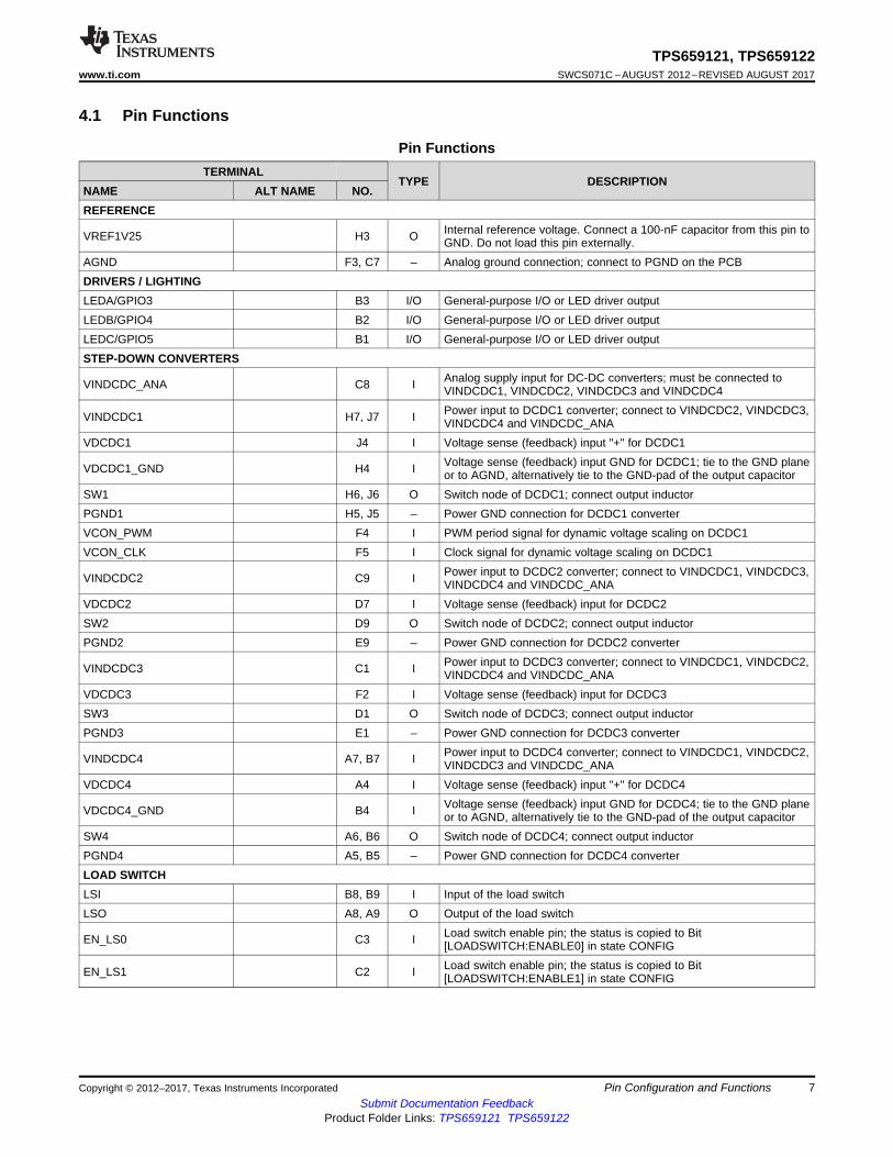
Pin FunctionsTERMINAL
TYPE DESCRIPTIONNAME ALT NAME NO.REFERENCE
VREF1V25 H3 O Internal reference voltage. Connect a 100-nF capacitor from this pin toGND. Do not load this pin externally.
AGND F3, C7 – Analog ground connection; connect to PGND on the PCBDRIVERS / LIGHTINGLEDA/GPIO3 B3 I/O General-purpose I/O or LED driver outputLEDB/GPIO4 B2 I/O General-purpose I/O or LED driver outputLEDC/GPIO5 B1 I/O General-purpose I/O or LED driver outputSTEP-DOWN CONVERTERS
VINDCDC_ANA C8 I Analog supply input for DC-DC converters; must be connected toVINDCDC1, VINDCDC2, VINDCDC3 and VINDCDC4
VINDCDC1 H7, J7 I Power input to DCDC1 converter; connect to VINDCDC2, VINDCDC3,VINDCDC4 and VINDCDC_ANA
VDCDC1 J4 I Voltage sense (feedback) input "+" for DCDC1
VDCDC1_GND H4 I Voltage sense (feedback) input GND for DCDC1; tie to the GND planeor to AGND, alternatively tie to the GND-pad of the output capacitor
SW1 H6, J6 O Switch node of DCDC1; connect output inductorPGND1 H5, J5 – Power GND connection for DCDC1 converterVCON_PWM F4 I PWM period signal for dynamic voltage scaling on DCDC1VCON_CLK F5 I Clock signal for dynamic voltage scaling on DCDC1
VINDCDC2 C9 I Power input to DCDC2 converter; connect to VINDCDC1, VINDCDC3,VINDCDC4 and VINDCDC_ANA
VDCDC2 D7 I Voltage sense (feedback) input for DCDC2SW2 D9 O Switch node of DCDC2; connect output inductorPGND2 E9 – Power GND connection for DCDC2 converter
VINDCDC3 C1 I Power input to DCDC3 converter; connect to VINDCDC1, VINDCDC2,VINDCDC4 and VINDCDC_ANA
VDCDC3 F2 I Voltage sense (feedback) input for DCDC3SW3 D1 O Switch node of DCDC3; connect output inductorPGND3 E1 – Power GND connection for DCDC3 converter
VINDCDC4 A7, B7 I Power input to DCDC4 converter; connect to VINDCDC1, VINDCDC2,VINDCDC3 and VINDCDC_ANA
VDCDC4 A4 I Voltage sense (feedback) input "+" for DCDC4
VDCDC4_GND B4 I Voltage sense (feedback) input GND for DCDC4; tie to the GND planeor to AGND, alternatively tie to the GND-pad of the output capacitor
SW4 A6, B6 O Switch node of DCDC4; connect output inductorPGND4 A5, B5 – Power GND connection for DCDC4 converterLOAD SWITCHLSI B8, B9 I Input of the load switchLSO A8, A9 O Output of the load switch
EN_LS0 C3 I Load switch enable pin; the status is copied to Bit[LOADSWITCH:ENABLE0] in state CONFIG
EN_LS1 C2 I Load switch enable pin; the status is copied to Bit[LOADSWITCH:ENABLE1] in state CONFIG
8
TPS659121, TPS659122SWCS071C –AUGUST 2012–REVISED AUGUST 2017 www.ti.com
Submit Documentation FeedbackProduct Folder Links: TPS659121 TPS659122
Pin Configuration and Functions Copyright © 2012–2017, Texas Instruments Incorporated
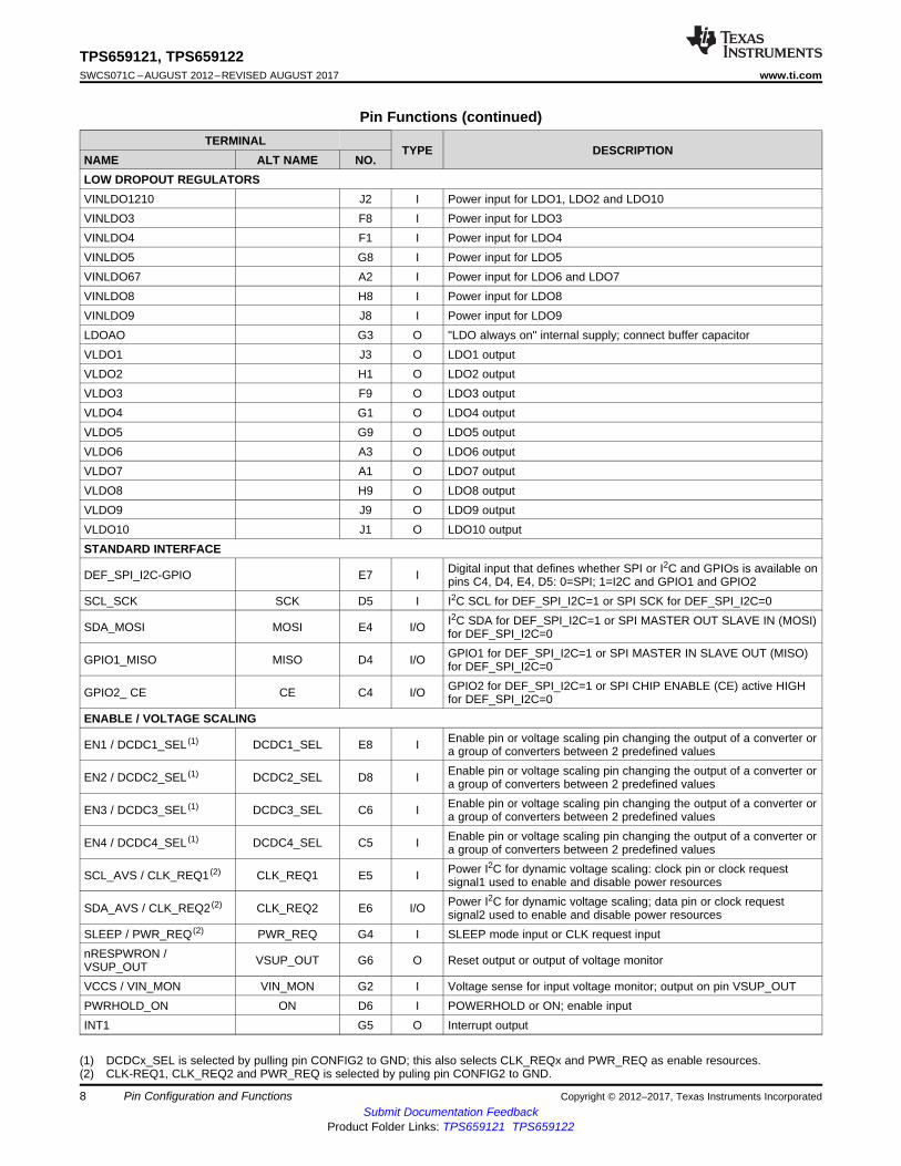
Pin Functions (continued)TERMINAL
TYPE DESCRIPTIONNAME ALT NAME NO.
(1) DCDCx_SEL is selected by pulling pin CONFIG2 to GND; this also selects CLK_REQx and PWR_REQ as enable resources.(2) CLK-REQ1, CLK_REQ2 and PWR_REQ is selected by puling pin CONFIG2 to GND.
LOW DROPOUT REGULATORSVINLDO1210 J2 I Power input for LDO1, LDO2 and LDO10VINLDO3 F8 I Power input for LDO3VINLDO4 F1 I Power input for LDO4VINLDO5 G8 I Power input for LDO5VINLDO67 A2 I Power input for LDO6 and LDO7VINLDO8 H8 I Power input for LDO8VINLDO9 J8 I Power input for LDO9LDOAO G3 O "LDO always on" internal supply; connect buffer capacitorVLDO1 J3 O LDO1 outputVLDO2 H1 O LDO2 outputVLDO3 F9 O LDO3 outputVLDO4 G1 O LDO4 outputVLDO5 G9 O LDO5 outputVLDO6 A3 O LDO6 outputVLDO7 A1 O LDO7 outputVLDO8 H9 O LDO8 outputVLDO9 J9 O LDO9 outputVLDO10 J1 O LDO10 outputSTANDARD INTERFACE
DEF_SPI_I2C-GPIO E7 I Digital input that defines whether SPI or I2C and GPIOs is available onpins C4, D4, E4, D5: 0=SPI; 1=I2C and GPIO1 and GPIO2
SCL_SCK SCK D5 I I2C SCL for DEF_SPI_I2C=1 or SPI SCK for DEF_SPI_I2C=0
SDA_MOSI MOSI E4 I/O I2C SDA for DEF_SPI_I2C=1 or SPI MASTER OUT SLAVE IN (MOSI)for DEF_SPI_I2C=0
GPIO1_MISO MISO D4 I/O GPIO1 for DEF_SPI_I2C=1 or SPI MASTER IN SLAVE OUT (MISO)for DEF_SPI_I2C=0
GPIO2_ CE CE C4 I/O GPIO2 for DEF_SPI_I2C=1 or SPI CHIP ENABLE (CE) active HIGHfor DEF_SPI_I2C=0
ENABLE / VOLTAGE SCALING
EN1 / DCDC1_SEL (1) DCDC1_SEL E8 I Enable pin or voltage scaling pin changing the output of a converter ora group of converters between 2 predefined values
EN2 / DCDC2_SEL (1) DCDC2_SEL D8 I Enable pin or voltage scaling pin changing the output of a converter ora group of converters between 2 predefined values
EN3 / DCDC3_SEL (1) DCDC3_SEL C6 I Enable pin or voltage scaling pin changing the output of a converter ora group of converters between 2 predefined values
EN4 / DCDC4_SEL (1) DCDC4_SEL C5 I Enable pin or voltage scaling pin changing the output of a converter ora group of converters between 2 predefined values
SCL_AVS / CLK_REQ1 (2) CLK_REQ1 E5 I Power I2C for dynamic voltage scaling: clock pin or clock requestsignal1 used to enable and disable power resources
SDA_AVS / CLK_REQ2 (2) CLK_REQ2 E6 I/O Power I2C for dynamic voltage scaling; data pin or clock requestsignal2 used to enable and disable power resources
SLEEP / PWR_REQ (2) PWR_REQ G4 I SLEEP mode input or CLK request inputnRESPWRON /VSUP_OUT VSUP_OUT G6 O Reset output or output of voltage monitor
VCCS / VIN_MON VIN_MON G2 I Voltage sense for input voltage monitor; output on pin VSUP_OUTPWRHOLD_ON ON D6 I POWERHOLD or ON; enable inputINT1 G5 O Interrupt output
9
TPS659121, TPS659122www.ti.com SWCS071C –AUGUST 2012–REVISED AUGUST 2017
Submit Documentation FeedbackProduct Folder Links: TPS659121 TPS659122
Pin Configuration and FunctionsCopyright © 2012–2017, Texas Instruments Incorporated
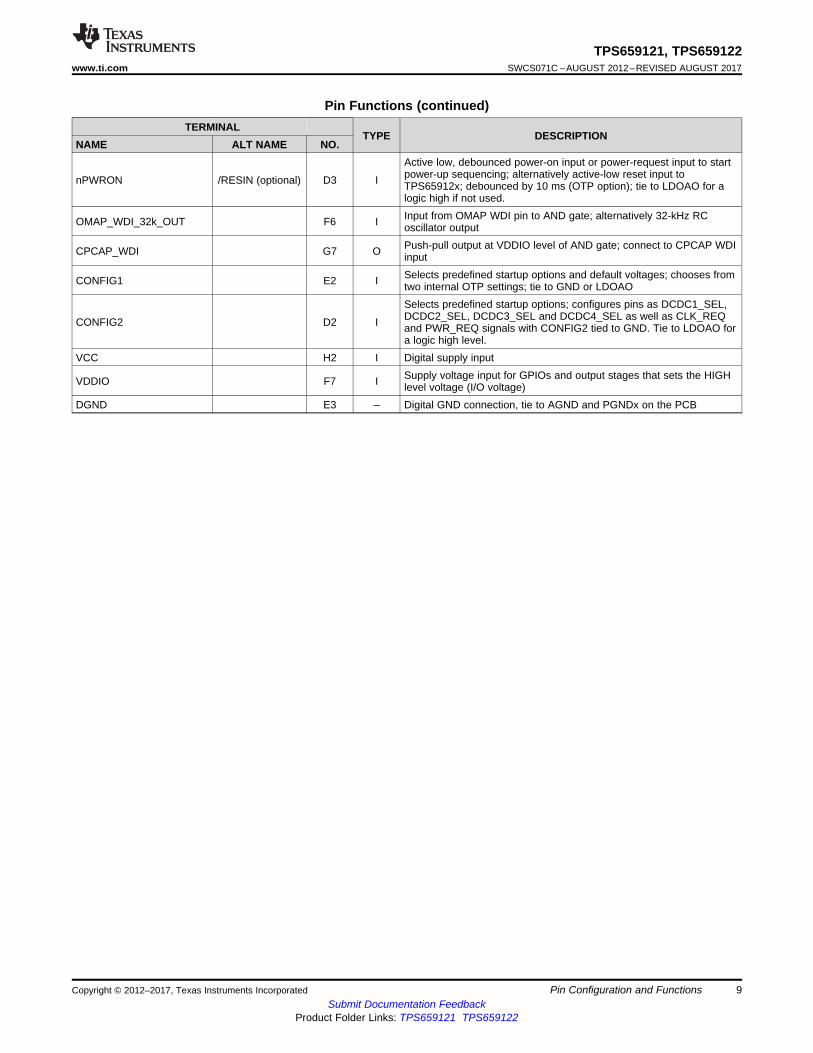
Pin Functions (continued)TERMINAL
TYPE DESCRIPTIONNAME ALT NAME NO.
nPWRON /RESIN (optional) D3 I
Active low, debounced power-on input or power-request input to startpower-up sequencing; alternatively active-low reset input toTPS65912x; debounced by 10 ms (OTP option); tie to LDOAO for alogic high if not used.
OMAP_WDI_32k_OUT F6 I Input from OMAP WDI pin to AND gate; alternatively 32-kHz RCoscillator output
CPCAP_WDI G7 O Push-pull output at VDDIO level of AND gate; connect to CPCAP WDIinput
CONFIG1 E2 I Selects predefined startup options and default voltages; chooses fromtwo internal OTP settings; tie to GND or LDOAO
CONFIG2 D2 I
Selects predefined startup options; configures pins as DCDC1_SEL,DCDC2_SEL, DCDC3_SEL and DCDC4_SEL as well as CLK_REQand PWR_REQ signals with CONFIG2 tied to GND. Tie to LDOAO fora logic high level.
VCC H2 I Digital supply input
VDDIO F7 I Supply voltage input for GPIOs and output stages that sets the HIGHlevel voltage (I/O voltage)
DGND E3 – Digital GND connection, tie to AGND and PGNDx on the PCB
10
TPS659121, TPS659122SWCS071C –AUGUST 2012–REVISED AUGUST 2017 www.ti.com
Submit Documentation FeedbackProduct Folder Links: TPS659121 TPS659122
Specifications Copyright © 2012–2017, Texas Instruments Incorporated
(1) Stresses beyond those listed under Absolute Maximum Ratings may cause permanent damage to the device. These are stress ratingsonly and functional operation of the device at these or any other conditions beyond those indicated under Section 5.3 is not implied.Exposure to absolute-maximum-rated conditions for extended periods may affect device reliability.
5 Specifications
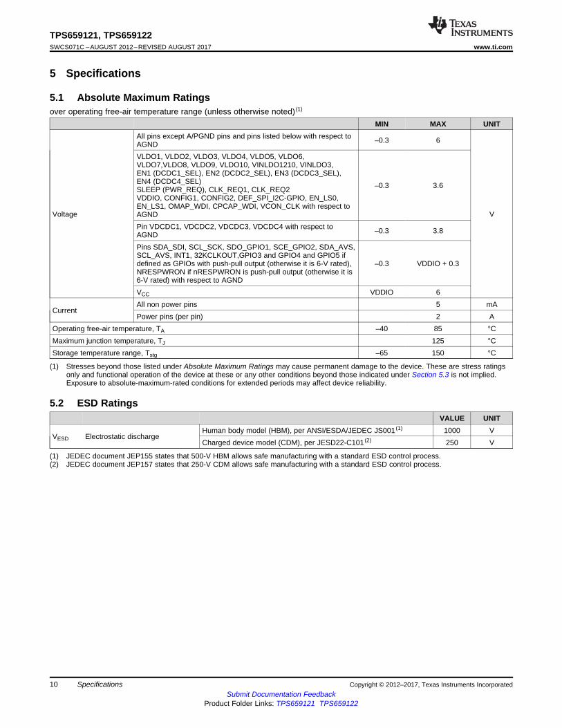
5.1 Absolute Maximum Ratingsover operating free-air temperature range (unless otherwise noted) (1)
MIN MAX UNIT
Voltage
All pins except A/PGND pins and pins listed below with respect toAGND –0.3 6
V
VLDO1, VLDO2, VLDO3, VLDO4, VLDO5, VLDO6,VLDO7,VLDO8, VLDO9, VLDO10, VINLDO1210, VINLDO3,EN1 (DCDC1_SEL), EN2 (DCDC2_SEL), EN3 (DCDC3_SEL),EN4 (DCDC4_SEL)SLEEP (PWR_REQ), CLK_REQ1, CLK_REQ2VDDIO, CONFIG1, CONFIG2, DEF_SPI_I2C-GPIO, EN_LS0,EN_LS1, OMAP_WDI, CPCAP_WDI, VCON_CLK with respect toAGND
–0.3 3.6
Pin VDCDC1, VDCDC2, VDCDC3, VDCDC4 with respect toAGND –0.3 3.8
Pins SDA_SDI, SCL_SCK, SDO_GPIO1, SCE_GPIO2, SDA_AVS,SCL_AVS, INT1, 32KCLKOUT,GPIO3 and GPIO4 and GPIO5 ifdefined as GPIOs with push-pull output (otherwise it is 6-V rated),NRESPWRON if nRESPWRON is push-pull output (otherwise it is6-V rated) with respect to AGND
–0.3 VDDIO + 0.3
VCC VDDIO 6
CurrentAll non power pins 5 mAPower pins (per pin) 2 A
Operating free-air temperature, TA –40 85 °CMaximum junction temperature, TJ 125 °CStorage temperature range, Tstg –65 150 °C
(1) JEDEC document JEP155 states that 500-V HBM allows safe manufacturing with a standard ESD control process.(2) JEDEC document JEP157 states that 250-V CDM allows safe manufacturing with a standard ESD control process.
5.2 ESD RatingsVALUE UNIT
VESD Electrostatic dischargeHuman body model (HBM), per ANSI/ESDA/JEDEC JS001 (1) 1000 VCharged device model (CDM), per JESD22-C101 (2) 250 V
11
TPS659121, TPS659122www.ti.com SWCS071C –AUGUST 2012–REVISED AUGUST 2017
Submit Documentation FeedbackProduct Folder Links: TPS659121 TPS659122
SpecificationsCopyright © 2012–2017, Texas Instruments Incorporated
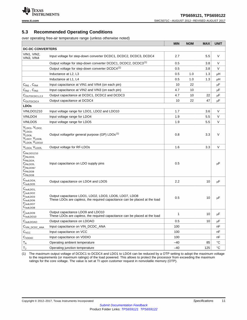
(1) The maximum output voltage of DCDC1 to DCDC4 and LDO1 to LDO4 can be reduced by a OTP setting to adopt the maximum voltageto the requirements (or maximum ratings) of the load powered. This allows to protect the processor from exceeding the maximumratings for the core voltage. The value is set at TI upon customer request in nonvolatile memory (OTP).
5.3 Recommended Operating Conditionsover operating free-air temperature range (unless otherwise noted)
MIN NOM MAX UNITDC-DC CONVERTERSVIN1, VIN2,VIN3, VIN4 Input voltage for step-down converter DCDC1, DCDC2, DCDC3, DCDC4 2.7 5.5 V
Output voltage for step-down converter DCDC1, DCDC2, DCDC3 (1) 0.5 3.8 VOutput voltage for step-down converter DCDC4 (1) 0.5 3.8 VInductance at L2, L3 0.5 1.0 1.3 μHInductance at L1, L4 0.5 1.0 1.3 μH
CIN1 , CIN4 Input capacitance at VIN1 and VIN4 (on each pin) 10 22 μFCIN2 , CIN3 Input capacitance at VIN2 and VIN3 (on each pin) 4.7 10 μFCOUTDCDC1,2,3 Output capacitance at DCDC1, DCDC2 and DCDC3 4.7 10 22 μFCOUTDCDC4 Output capacitance at DCDC4 10 22 47 μFLDOsVINLDO1210 Input voltage range for LDO1, LDO2 and LDO10 1.7 3.6 VVINLDO4 Input voltage range for LDO4 1.9 5.5 VVINLDO5 Input voltage range for LDO5 1.9 5.5 VVLDO1, VLDO2,VLDO3,VLDO6,VLDO7, VLDO8,VLDO9, VLDO10
Output voltagefor general purpose (GP) LDOs (1) 0.8 3.3 V
VLDO4, VLDO5, Output voltage for RF-LDOs 1.6 3.3 VCINLDO1210CINLDO3,CINLDO4,CINLDO5,CINLDO67CINLDO8CINLDO8
Input capacitance on LDO supply pins 0.5 μF
CoutLDO4,CoutLDO5
Output capacitance on LDO4 and LDO5 2.2 10 μF
CoutLDO1,CoutLDO2CoutLDO3CoutLDO6CoutLDO7CoutLDO8
Output capacitance LDO1, LDO2, LDO3, LDO6, LDO7, LDO8These LDOs are capless, the required capacitance can be placed at the load 0.5 10 μF
CoutLDO9CoutLDO10
Output capacitance LDO9 and LDO10These LDOs are capless, the required capacitance can be placed at the load 1 10 μF
CoutLDOAO Output capacitance on LDOAO 0.5 10 μFCVIN_DCDC_ANA Input capacitance on VIN_DCDC_ANA 100 nFCVCC Input capacitance on VCC 100 nFCVDDIO Input capacitance on VDDIO 100 nFTA Operating ambient temperature –40 85 °CTJ Operating junction temperature –40 125 °C
12
TPS659121, TPS659122SWCS071C –AUGUST 2012–REVISED AUGUST 2017 www.ti.com
Submit Documentation FeedbackProduct Folder Links: TPS659121 TPS659122
Specifications Copyright © 2012–2017, Texas Instruments Incorporated
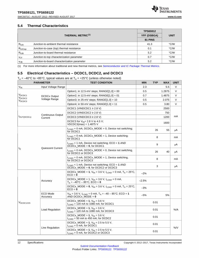
(1) For more information about traditional and new thermal metrics, see Semiconductor and IC Package Thermal Metrics.
5.4 Thermal Characteristics
THERMAL METRIC (1)TPS65912
UNITYFF (DSBGA)81 PINS
RθJA Junction-to-ambient thermal resistance 41.3 °C/WRθJCtop Junction-to-case (top) thermal resistance 0.1 °C/WRθJB Junction-to-board thermal resistance 5.2 °C/WψJT Junction-to-top characterization parameter 0.7 °C/WψJB Junction-to-board characterization parameter 5.2 °C/W
5.5 Electrical Characteristics – DCDC1, DCDC2, and DCDC3TA = –40°C to +85°C, typical values are at TA = +25°C (unless otherwise noted)
PARAMETER TEST CONDITION MIN TYP MAX UNITVIN Input Voltage Range 2.3 5.5 V
VDCDC1VDCDC2VDCDC3
DCDCx OutputVoltage Range
Option1; in 12.5-mV steps; RANGE[1,0] = 00 0.5 1.2875 VOption2; in 12.5-mV steps; RANGE[1,0] = 01 0.7 1.4875 VOption3; in 25-mV steps; RANGE[1,0] = 10 0.5 2.075 VOption4; in 50-mV steps; RANGE[1,0] = 11 0.5 3.80 V
IOUT(DCDCx)Continuous OutputCurrent
DCDC1 (VINDCDC1 ≥ 2.8 V) 2500
mADCDC2 (VINDCDC2 ≥ 2.8 V) 750DCDC3 (VINDCDC3 ≥ 2.8 V) 1200DCDC3 for VIN= 2.8 V to 4.5 V;VDCDC3(max) = 1.4875 V 1600
IQ Quiescent Current
ILOAD = 0 mA, DCDCx_MODE = 0, Device not switching;for DCDC1 26 55 μA
ILOAD = 0 mA, DCDCx_MODE = 1, Device switching;for DCDC1 8 mA
ILOAD < 1 mA, Device not switching; ECO = 1 ANDDCDCx_MODE = 0, for DCDC1 9 μA
ILOAD = 0 mA, DCDCx_MODE = 0, Device not switching,for DCDC2 or DCDC3 26 40 μA
ILOAD = 0 mA, DCDCx_MODE = 1, Device switching,for DCDC2 or DCDC3 8 mA
ILOAD < 1 mA, Device not switching; ECO = 1 ANDDCDCx_MODE = 0, for DCDC2 or DCDC3 3 μA
VDCDC1/2/3
Accuracy
DCDCx_MODE = 1, VIN = 3.6 V, ILOAD = 0 mA, TA = 25°C,ECO = 0 –2%
DCDCx_MODE = 1, VIN = 3.6 V, ILOAD = 0 mA,TA = –40°C – 85°C, ECO = 0 –2.5%
DCDCx_MODE = 0, VIN = 3.6 V, ILOAD = 0 mA, TA = 25°C,ECO = 0 –3%
ECO ModeAccuracy
VIN = 3.6 V, ILOAD = 0 mA, TA = –40 – 85°C; ECO = 1AND DCDCx_MODE = 0 –5% 5%
Load Regulation
DCDCx_MODE = 1, VIN = 3.6 V;ILOAD = 120 mA to 1080 mA; for DCDC1 0.01
%/ADCDCx_MODE = 1, VIN = 3.6 V;ILOAD = 120 mA to 1080 mA; for DCDC3 0.01
DCDCx_MODE = 1, VIN = 3.6 V;ILOAD = 50 mA to 450 mA; for DCDC2 0.01
Line Regulation
DCDCx_MODE = 1, VIN = 2.5 to 5.5 V,ILOAD = 0 mA, for DCDC1 0.01
%/VDCDCx_MODE = 1, VIN = 2.5 to 5.5 V,ILOAD = 0 mA, for DCDC2 or DCDC3 0.01
13
TPS659121, TPS659122www.ti.com SWCS071C –AUGUST 2012–REVISED AUGUST 2017
Submit Documentation FeedbackProduct Folder Links: TPS659121 TPS659122
SpecificationsCopyright © 2012–2017, Texas Instruments Incorporated
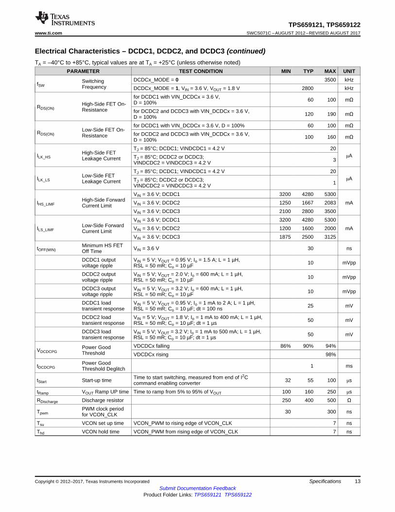
Electrical Characteristics – DCDC1, DCDC2, and DCDC3 (continued)TA = –40°C to +85°C, typical values are at TA = +25°C (unless otherwise noted)
PARAMETER TEST CONDITION MIN TYP MAX UNIT
fSWSwitchingFrequency
DCDCx_MODE = 0 3500 kHzDCDCx_MODE = 1, VIN = 3.6 V, VOUT = 1.8 V 2800 kHz
RDS(ON)High-Side FET On-Resistance
for DCDC1 with VIN_DCDCx = 3.6 V,D = 100% 60 100 mΩ
for DCDC2 and DCDC3 with VIN_DCDCx = 3.6 V,D = 100% 120 190 mΩ
RDS(ON)Low-Side FET On-Resistance
for DCDC1 with VIN_DCDCx = 3.6 V, D = 100% 60 100 mΩfor DCDC2 and DCDC3 with VIN_DCDCx = 3.6 V,D = 100% 100 160 mΩ
ILK_HSHigh-Side FETLeakage Current
TJ = 85°C; DCDC1; VINDCDC1 = 4.2 V 20μATJ = 85°C; DCDC2 or DCDC3;
VINDCDC2 = VINDCDC3 = 4.2 V 3
ILK_LSLow-Side FETLeakage Current
TJ = 85°C; DCDC1; VINDCDC1 = 4.2 V 20μATJ = 85°C; DCDC2 or DCDC3;
VINDCDC2 = VINDCDC3 = 4.2 V 1
IHS_LIMFHigh-Side ForwardCurrent Limit
VIN = 3.6 V; DCDC1 3200 4280 5300mAVIN = 3.6 V; DCDC2 1250 1667 2083
VIN = 3.6 V; DCDC3 2100 2800 3500
ILS_LIMFLow-Side ForwardCurrent Limit
VIN = 3.6 V; DCDC1 3200 4280 5300mAVIN = 3.6 V; DCDC2 1200 1600 2000
VIN = 3.6 V; DCDC3 1875 2500 3125
tOFF(MIN)Minimum HS FETOff Time VIN = 3.6 V 30 ns
DCDC1 outputvoltage ripple
VIN = 5 V; VOUT = 0.95 V; Io = 1.5 A; L = 1 µH,RSL = 50 mR; Co = 10 µF 10 mVpp
DCDC2 outputvoltage ripple
VIN = 5 V; VOUT = 2.0 V; Io = 600 mA; L = 1 µH,RSL = 50 mR; Co = 10 µF 10 mVpp
DCDC3 outputvoltage ripple
VIN = 5 V; VOUT = 3.2 V; Io = 600 mA; L = 1 µH,RSL = 50 mR; Co = 10 µF 10 mVpp
DCDC1 loadtransient response
VIN = 5 V; VOUT = 0.95 V; Io = 1 mA to 2 A; L = 1 µH,RSL = 50 mR; Co = 10 µF; dt = 100 ns 25 mV
DCDC2 loadtransient response
VIN = 5 V; VOUT = 1.8 V; Io = 1 mA to 400 mA; L = 1 µH,RSL = 50 mR; Co = 10 µF; dt = 1 µs 50 mV
DCDC3 loadtransient response
VIN = 5 V; VOUT = 3.2 V; Io = 1 mA to 500 mA; L = 1 µH,RSL = 50 mR; Co = 10 µF; dt = 1 µs 50 mV
VDCDCPGPower GoodThreshold
VDCDCx falling 86% 90% 94%VDCDCx rising 98%
tDCDCPGPower GoodThreshold Deglitch 1 ms
tStart Start-up time Time to start switching, measured from end of I2Ccommand enabling converter 32 55 100 μs
tRamp VOUT Ramp UP time Time to ramp from 5% to 95% of VOUT 100 160 250 μsRDischarge Discharge resistor 250 400 500 Ω
TpwmPWM clock periodfor VCON_CLK 30 300 ns
Tsu VCON set up time VCON_PWM to rising edge of VCON_CLK 7 nsThd VCON hold time VCON_PWM from rising edge of VCON_CLK 7 ns
14
TPS659121, TPS659122SWCS071C –AUGUST 2012–REVISED AUGUST 2017 www.ti.com
Submit Documentation FeedbackProduct Folder Links: TPS659121 TPS659122
Specifications Copyright © 2012–2017, Texas Instruments Incorporated
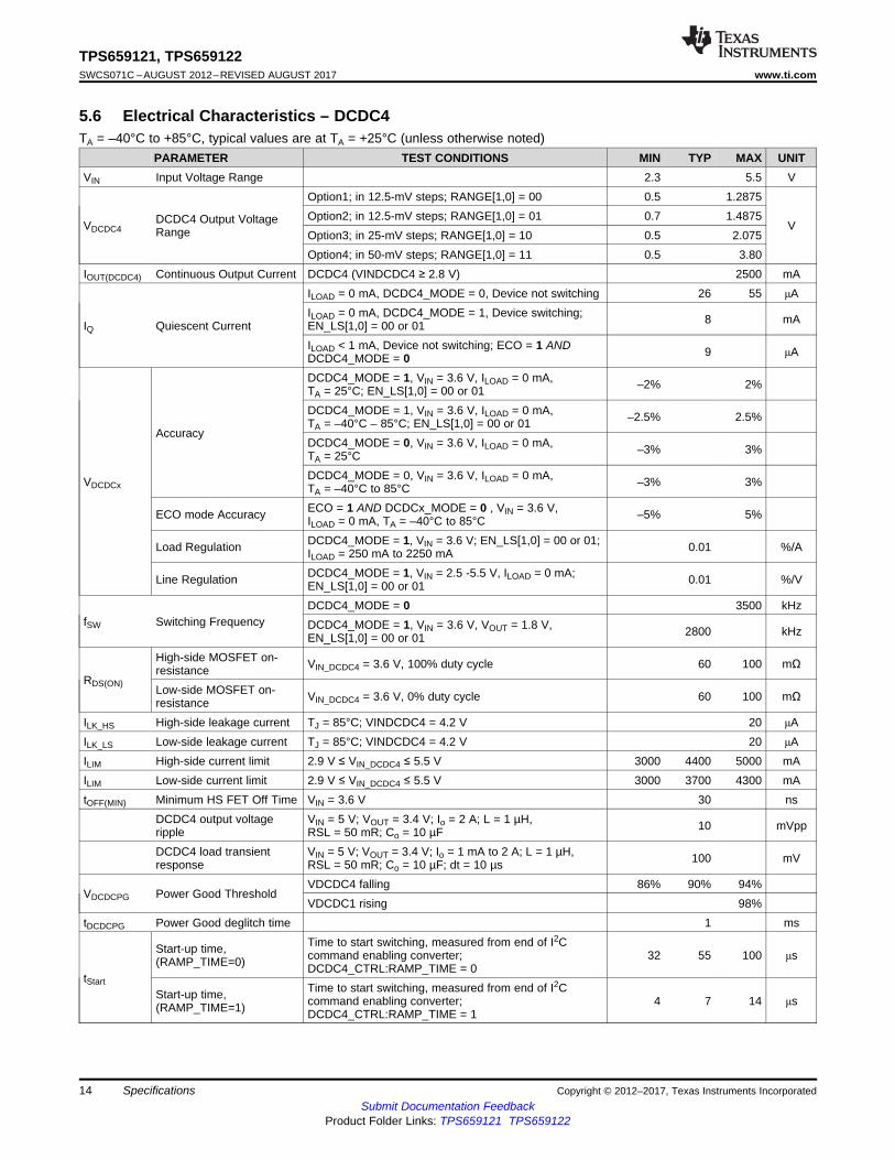
5.6 Electrical Characteristics – DCDC4TA = –40°C to +85°C, typical values are at TA = +25°C (unless otherwise noted)
PARAMETER TEST CONDITIONS MIN TYP MAX UNITVIN Input Voltage Range 2.3 5.5 V
VDCDC4DCDC4 Output VoltageRange
Option1; in 12.5-mV steps; RANGE[1,0] = 00 0.5 1.2875
VOption2; in 12.5-mV steps; RANGE[1,0] = 01 0.7 1.4875Option3; in 25-mV steps; RANGE[1,0] = 10 0.5 2.075Option4; in 50-mV steps; RANGE[1,0] = 11 0.5 3.80
IOUT(DCDC4) Continuous Output Current DCDC4 (VINDCDC4 ≥ 2.8 V) 2500 mA
IQ Quiescent Current
ILOAD = 0 mA, DCDC4_MODE = 0, Device not switching 26 55 μAILOAD = 0 mA, DCDC4_MODE = 1, Device switching;EN_LS[1,0] = 00 or 01 8 mA
ILOAD < 1 mA, Device not switching; ECO = 1 ANDDCDC4_MODE = 0 9 μA
VDCDCx
Accuracy
DCDC4_MODE = 1, VIN = 3.6 V, ILOAD = 0 mA,TA = 25°C; EN_LS[1,0] = 00 or 01 –2% 2%
DCDC4_MODE = 1, VIN = 3.6 V, ILOAD = 0 mA,TA = –40°C – 85°C; EN_LS[1,0] = 00 or 01 –2.5% 2.5%
DCDC4_MODE = 0, VIN = 3.6 V, ILOAD = 0 mA,TA = 25°C –3% 3%
DCDC4_MODE = 0, VIN = 3.6 V, ILOAD = 0 mA,TA = –40°C to 85°C –3% 3%
ECO mode Accuracy ECO = 1 AND DCDCx_MODE = 0 , VIN = 3.6 V,ILOAD = 0 mA, TA = –40°C to 85°C –5% 5%
Load Regulation DCDC4_MODE = 1, VIN = 3.6 V; EN_LS[1,0] = 00 or 01;ILOAD = 250 mA to 2250 mA 0.01 %/A
Line Regulation DCDC4_MODE = 1, VIN = 2.5 -5.5 V, ILOAD = 0 mA;EN_LS[1,0] = 00 or 01 0.01 %/V
fSW Switching FrequencyDCDC4_MODE = 0 3500 kHzDCDC4_MODE = 1, VIN = 3.6 V, VOUT = 1.8 V,EN_LS[1,0] = 00 or 01 2800 kHz
RDS(ON)
High-side MOSFET on-resistance VIN_DCDC4 = 3.6 V, 100% duty cycle 60 100 mΩ
Low-side MOSFET on-resistance VIN_DCDC4 = 3.6 V, 0% duty cycle 60 100 mΩ
ILK_HS High-side leakage current TJ = 85°C; VINDCDC4 = 4.2 V 20 μAILK_LS Low-side leakage current TJ = 85°C; VINDCDC4 = 4.2 V 20 μAILIM High-side current limit 2.9 V ≤ VIN_DCDC4 ≤ 5.5 V 3000 4400 5000 mAILIM Low-side current limit 2.9 V ≤ VIN_DCDC4 ≤ 5.5 V 3000 3700 4300 mAtOFF(MIN) Minimum HS FET Off Time VIN = 3.6 V 30 ns
DCDC4 output voltageripple
VIN = 5 V; VOUT = 3.4 V; Io = 2 A; L = 1 µH,RSL = 50 mR; Co = 10 µF 10 mVpp
DCDC4 load transientresponse
VIN = 5 V; VOUT = 3.4 V; Io = 1 mA to 2 A; L = 1 µH,RSL = 50 mR; Co = 10 µF; dt = 10 µs 100 mV
VDCDCPG Power Good ThresholdVDCDC4 falling 86% 90% 94%VDCDC1 rising 98%
tDCDCPG Power Good deglitch time 1 ms
tStart
Start-up time,(RAMP_TIME=0)
Time to start switching, measured from end of I2Ccommand enabling converter;DCDC4_CTRL:RAMP_TIME = 0
32 55 100 μs
Start-up time,(RAMP_TIME=1)
Time to start switching, measured from end of I2Ccommand enabling converter;DCDC4_CTRL:RAMP_TIME = 1
4 7 14 μs
15
TPS659121, TPS659122www.ti.com SWCS071C –AUGUST 2012–REVISED AUGUST 2017
Submit Documentation FeedbackProduct Folder Links: TPS659121 TPS659122
SpecificationsCopyright © 2012–2017, Texas Instruments Incorporated
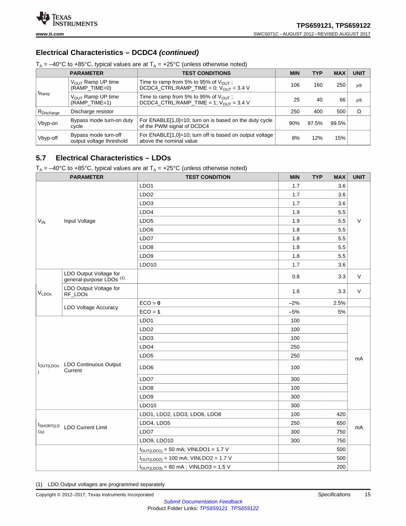
Electrical Characteristics – DCDC4 (continued)TA = –40°C to +85°C, typical values are at TA = +25°C (unless otherwise noted)
PARAMETER TEST CONDITIONS MIN TYP MAX UNIT
tRamp
VOUT Ramp UP time(RAMP_TIME=0)
Time to ramp from 5% to 95% of VOUT ;DCDC4_CTRL:RAMP_TIME = 0; VOUT = 3.4 V 106 160 250 μs
VOUT Ramp UP time(RAMP_TIME=1)
Time to ramp from 5% to 95% of VOUT ;DCDC4_CTRL:RAMP_TIME = 1; VOUT = 3.4 V 25 40 66 μs
RDischarge Discharge resistor 250 400 500 Ω
Vbyp-on Bypass mode turn-on dutycycle
For ENABLE[1,0]=10; turn on is based on the duty cycleof the PWM signal of DCDC4 90% 97.5% 99.5%
Vbyp-off Bypass mode turn-offoutput voltage threshold
For ENABLE[1,0]=10; turn off is based on output voltageabove the nominal value 8% 12% 15%
(1) LDO Output voltages are programmed separately
5.7 Electrical Characteristics – LDOsTA = –40°C to +85°C, typical values are at TA = +25°C (unless otherwise noted)
PARAMETER TEST CONDITION MIN TYP MAX UNITLDO1 1.7 3.6LDO2 1.7 3.6LDO3 1.7 3.6LDO4 1.9 5.5
VIN Input Voltage LDO5 1.9 5.5 VLDO6 1.8 5.5LDO7 1.8 5.5LDO8 1.8 5.5LDO9 1.8 5.5LDO10 1.7 3.6
VLDOx
LDO Output Voltage forgeneral-purpose LDOs (1) 0.8 3.3 V
LDO Output Voltage forRF_LDOs 1.6 3.3 V
LDO Voltage AccuracyECO = 0 –2% 2.5%ECO = 1 –5% 5%LDO1 100LDO2 100LDO3 100LDO4 250
mALDO5 250IOUT(LDOx)
LDO Continuous OutputCurrent LDO6 100
LDO7 300LDO8 100LDO9 300LDO10 300
ISHORT(LDOx)
LDO Current Limit
LDO1, LDO2, LDO3, LDO6, LDO8 100 420
mALDO4, LDO5 250 650LDO7 300 750LDO9, LDO10 300 750IOUT(LDO1) = 50 mA; VINLDO1 = 1.7 V 500IOUT(LDO2) = 100 mA; VINLDO2 = 1.7 V 500IOUT(LDO3) = 80 mA ; VINLDO3 = 1.5 V 200
16
TPS659121, TPS659122SWCS071C –AUGUST 2012–REVISED AUGUST 2017 www.ti.com
Submit Documentation FeedbackProduct Folder Links: TPS659121 TPS659122
Specifications Copyright © 2012–2017, Texas Instruments Incorporated
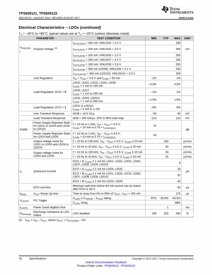
Electrical Characteristics – LDOs (continued)TA = –40°C to +85°C, typical values are at TA = +25°C (unless otherwise noted)
PARAMETER TEST CONDITION MIN TYP MAX UNIT
(2) VDO = VIN – VOUT, where VOUT = VOUT(NOM) – 2%
IOUT(LDO4) = 200 mA; VINLDO4 = 2.0 V 200VDO(LDOx)
Dropout Voltage (2) IOUT(LDO5) = 200 mA; VINLDO5 = 3.0 V 300 mV
IOUT(LDO6) = 100 mA; VINLDO6 = 3.2 V 200IOUT(LDO7) = 200 mA; VINLDO7 = 3.2 V 200IOUT(LDO8) = 100 mA; VINLDO8 = 2.9 V 200IOUT(LDO9) = 300 mA (LDO9); VINLDO9 = 3.1 V 200IOUT(LDO10) = 300 mA (LDO10); VINLDO10 = 2.0 V 200
Line Regulation VIN = VLDO + 0.5 V and ILOAD = 50 mA –1% 1%
Load Regulation; ECO = 0
LDO1, LDO2, LDO3, LDO6, LDO8:ILOAD = 1 mA to 100 mA –0.5% 0.5%
LDO5, LDO7:ILOAD = 1 mA to 200 mA –1% 1%
LDO4, LDO9, LDO10:ILOAD = 1 mA to 300 mA –1.5% 1.5%
Load Regulation; ECO = 1 LDO1 to LDO10:ILOAD = 0 mA to 1 mA –5% 5%
Line Transient Response dV/dt = ±0.5 V/μs –50 50 mVLoad Transient Response dI/dt = 100 mA/μs; 10% to 90% load step –110 110 mV
PSRR
Power Supply Rejection Ratiofor LDO1 to LDO3 and LDO6to LDO10
f = 10 Hz to 1 kHz, VIN – VOUT ≥ 0.5 V,ILOAD = 10 mA to 0.75 × ILOAD(MAX)
47dB
Power Supply Rejection Ratiofor LDO4 and LDO5
f = 10 Hz to 1 kHz, VIN – VOUT ≥ 0.5 V,ILOAD = 10 mA to 0.75 × ILOAD(MAX)
63
Output voltage noise forLDO1 to LDO3 and LDO6 toLDO10
f = 10 Hz to 100 kHz, VIN – VOUT ≥ 0.5 V, ILOAD ≥ 10 mA 150 µVrms
f = 10 Hz to 10 kHz, VIN – VOUT ≥ 0.5 V, ILOAD ≥ 10 mA 50 µVrms
Output voltage noise forLDO4 and LDO5
f = 10 Hz to 100 kHz, VIN – VOUT ≥ 0.5 V, ILOAD ≥ 10 mA 30 µVrmsf = 10 Hz to 10 kHz, VIN – VOUT ≥ 0.5 V, ILOAD ≥ 10 mA 15 µVrms
Iq Quiescent Current
ECO = 1; ILOAD ≤ 1 mA for LDO1, LDO2, LDO3, LDO6,LDO7, LDO8, LDO9, LDO10 8
µAECO = 1; ILOAD ≤ 1 mA for LDO4, LDO5 16ECO = 0; ILOAD ≤ 1 mA for LDO1, LDO2, LDO3, LDO6,LDO7, LDO8, LDO9, LDO10 32
ECO = 0; ILOAD ≤ 1 mA for LDO4, LDO5 40
ECO exit time Minimum wait time before the full current can be drawnafter ECO is set 0 50 µs
tRamp VOUT Ramp Up time Time to ramp from 5% to 95% of VOUT ; IOUT = 100 mA 170 µs
VLDOPG PG TriggerVLDOx ≤ VTARGET ; VLDOx falling 87% 90.6% 94.5%VLDOx rising 98%
tLDOPG Power Good deglitch time 1 ms
RDischargeDischarge resistance at LDOoutput LDO disabled 200 325 450 Ω
17
TPS659121, TPS659122www.ti.com SWCS071C –AUGUST 2012–REVISED AUGUST 2017
Submit Documentation FeedbackProduct Folder Links: TPS659121 TPS659122
SpecificationsCopyright © 2012–2017, Texas Instruments Incorporated
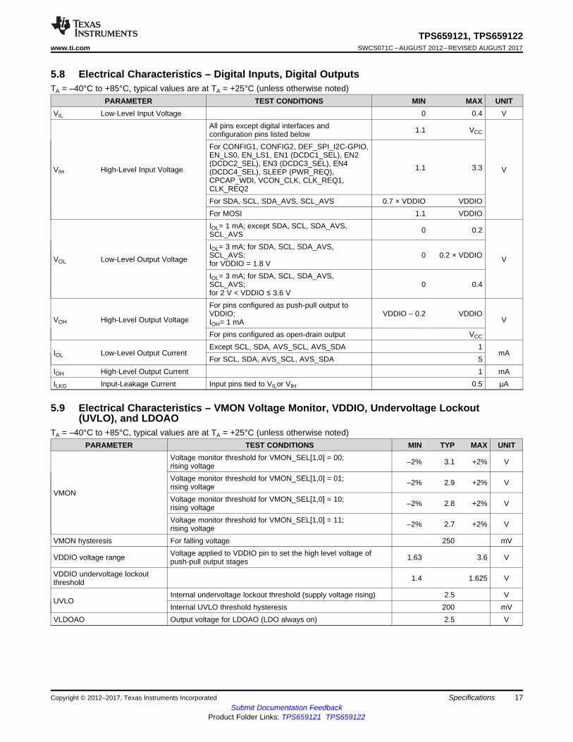
5.8 Electrical Characteristics – Digital Inputs, Digital OutputsTA = –40°C to +85°C, typical values are at TA = +25°C (unless otherwise noted)
PARAMETER TEST CONDITIONS MIN MAX UNITVIL Low-Level Input Voltage 0 0.4 V
VIH High-Level Input Voltage
All pins except digital interfaces andconfiguration pins listed below 1.1 VCC
V
For CONFIG1, CONFIG2, DEF_SPI_I2C-GPIO,EN_LS0, EN_LS1, EN1 (DCDC1_SEL), EN2(DCDC2_SEL), EN3 (DCDC3_SEL), EN4(DCDC4_SEL), SLEEP (PWR_REQ),CPCAP_WDI, VCON_CLK, CLK_REQ1,CLK_REQ2
1.1 3.3
For SDA, SCL, SDA_AVS, SCL_AVS 0.7 × VDDIO VDDIOFor MOSI 1.1 VDDIO
VOL Low-Level Output Voltage
IOL= 1 mA; except SDA, SCL, SDA_AVS,SCL_AVS 0 0.2
V
IOL= 3 mA; for SDA, SCL, SDA_AVS,SCL_AVS;for VDDIO = 1.8 V
0 0.2 × VDDIO
IOL= 3 mA; for SDA, SCL, SDA_AVS,SCL_AVS;for 2 V < VDDIO ≤ 3.6 V
0 0.4
VOH High-Level Output Voltage
For pins configured as push-pull output toVDDIO;IOH= 1 mA
VDDIO – 0.2 VDDIOV
For pins configured as open-drain output VCC
IOL Low-Level Output CurrentExcept SCL, SDA, AVS_SCL, AVS_SDA 1
mAFor SCL, SDA, AVS_SCL, AVS_SDA 5
IOH High-Level Output Current 1 mAILKG Input-Leakage Current Input pins tied to VILor VIH 0.5 µA
5.9 Electrical Characteristics – VMON Voltage Monitor, VDDIO, Undervoltage Lockout(UVLO), and LDOAO
TA = –40°C to +85°C, typical values are at TA = +25°C (unless otherwise noted)PARAMETER TEST CONDITIONS MIN TYP MAX UNIT
VMON
Voltage monitor threshold for VMON_SEL[1,0] = 00;rising voltage –2% 3.1 +2% V
Voltage monitor threshold for VMON_SEL[1,0] = 01;rising voltage –2% 2.9 +2% V
Voltage monitor threshold for VMON_SEL[1,0] = 10;rising voltage –2% 2.8 +2% V
Voltage monitor threshold for VMON_SEL[1,0] = 11;rising voltage –2% 2.7 +2% V
VMON hysteresis For falling voltage 250 mV
VDDIO voltage range Voltage applied to VDDIO pin to set the high level voltage ofpush-pull output stages 1.63 3.6 V
VDDIO undervoltage lockoutthreshold 1.4 1.625 V
UVLOInternal undervoltage lockout threshold (supply voltage rising) 2.5 VInternal UVLO threshold hysteresis 200 mV
VLDOAO Output voltage for LDOAO (LDO always on) 2.5 V
18
TPS659121, TPS659122SWCS071C –AUGUST 2012–REVISED AUGUST 2017 www.ti.com
Submit Documentation FeedbackProduct Folder Links: TPS659121 TPS659122
Specifications Copyright © 2012–2017, Texas Instruments Incorporated
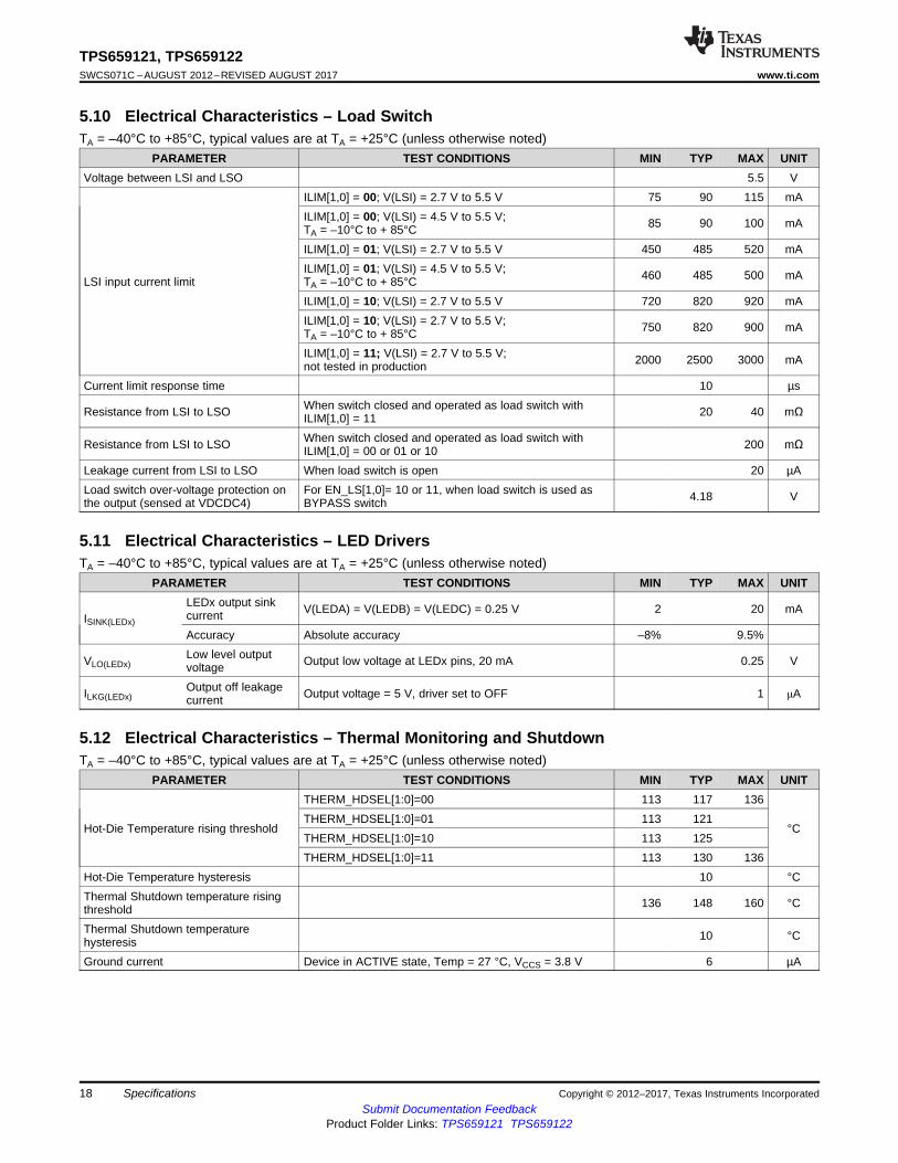
5.10 Electrical Characteristics – Load SwitchTA = –40°C to +85°C, typical values are at TA = +25°C (unless otherwise noted)
PARAMETER TEST CONDITIONS MIN TYP MAX UNITVoltage between LSI and LSO 5.5 V
LSI input current limit
ILIM[1,0] = 00; V(LSI) = 2.7 V to 5.5 V 75 90 115 mAILIM[1,0] = 00; V(LSI) = 4.5 V to 5.5 V;TA = –10°C to + 85°C 85 90 100 mA
ILIM[1,0] = 01; V(LSI) = 2.7 V to 5.5 V 450 485 520 mAILIM[1,0] = 01; V(LSI) = 4.5 V to 5.5 V;TA = –10°C to + 85°C 460 485 500 mA
ILIM[1,0] = 10; V(LSI) = 2.7 V to 5.5 V 720 820 920 mAILIM[1,0] = 10; V(LSI) = 2.7 V to 5.5 V;TA = –10°C to + 85°C 750 820 900 mA
ILIM[1,0] = 11; V(LSI) = 2.7 V to 5.5 V;not tested in production 2000 2500 3000 mA
Current limit response time 10 µs
Resistance from LSI to LSO When switch closed and operated as load switch withILIM[1,0] = 11 20 40 mΩ
Resistance from LSI to LSO When switch closed and operated as load switch withILIM[1,0] = 00 or 01 or 10 200 mΩ
Leakage current from LSI to LSO When load switch is open 20 µALoad switch over-voltage protection onthe output (sensed at VDCDC4)
For EN_LS[1,0]= 10 or 11, when load switch is used asBYPASS switch 4.18 V
5.11 Electrical Characteristics – LED DriversTA = –40°C to +85°C, typical values are at TA = +25°C (unless otherwise noted)
PARAMETER TEST CONDITIONS MIN TYP MAX UNIT
ISINK(LEDx)
LEDx output sinkcurrent V(LEDA) = V(LEDB) = V(LEDC) = 0.25 V 2 20 mA
Accuracy Absolute accuracy –8% 9.5%
VLO(LEDx)Low level outputvoltage Output low voltage at LEDx pins, 20 mA 0.25 V
ILKG(LEDx)Output off leakagecurrent Output voltage = 5 V, driver set to OFF 1 μA
5.12 Electrical Characteristics – Thermal Monitoring and ShutdownTA = –40°C to +85°C, typical values are at TA = +25°C (unless otherwise noted)
PARAMETER TEST CONDITIONS MIN TYP MAX UNIT
Hot-Die Temperature rising threshold
THERM_HDSEL[1:0]=00 113 117 136
°CTHERM_HDSEL[1:0]=01 113 121THERM_HDSEL[1:0]=10 113 125THERM_HDSEL[1:0]=11 113 130 136
Hot-Die Temperature hysteresis 10 °CThermal Shutdown temperature risingthreshold 136 148 160 °C
Thermal Shutdown temperaturehysteresis 10 °C
Ground current Device in ACTIVE state, Temp = 27 °C, VCCS = 3.8 V 6 µA
19
TPS659121, TPS659122www.ti.com SWCS071C –AUGUST 2012–REVISED AUGUST 2017
Submit Documentation FeedbackProduct Folder Links: TPS659121 TPS659122
SpecificationsCopyright © 2012–2017, Texas Instruments Incorporated
5.13 Electrical Characteristics – 32-kHz RC ClockTA = –40°C to +85°C, typical values are at TA = +25°C (unless otherwise noted)
PARAMETER TEST CONDITIONS MIN TYP MAX UNITCLK32KOUT rise and fall time CL = 35 pF 10 nsOutput-frequency low level outputvoltage CK32KOUT output 32 kHz
Output-frequency accuracy at 25°C –20% 0% +15%Output duty cycle 40% 50% 60%Settling time 150 µs
5.14 SPI Interface Timing RequirementsMIN MAX UNIT
tcesu Chip select set up time 30 nstcehld Chip select hold time 30 nstckper Clock cycle time 65 nstckhigh Clock high typical pulse duration 20 nstcklow Clock low typical pulse duration 20 nstsisu Input data set up time, before clock active edge 5 nstsihld Input data hold time, after clock active edge 5 nstdr Data retention time 15 nstCE Time from CE going low to CE going high 65 ns
Capacitive load on pin GPIO1_MISO 30 pF
(1) Specified by design. Not tested in production.
5.15 I2C Interface Timing Requirements (1)
MIN MAX UNIT
f(SCL) SCL Clock Frequency
Standard mode 100 kHzFast mode 400 kHzHigh-speed mode (write operation),CB – 100 pF max 3.4 MHz
High-speed mode (read operation),CB – 100 pF max 3.4 MHz
High-speed mode (write operation),CB – 400 pF max 1.7 MHz
High-speed mode (read operation),CB – 400 pF max 1.7 MHz
tBUFBus Free Time Between a STOPand START Condition
Standard mode 4.7 μsFast mode 1.3 μs
tHD, tSTAHold Time (Repeated) STARTCondition
Standard mode 4 μsFast mode 600 nsHigh-speed mode 160 ns
tLOW LOW Period of the SCL Clock
Standard mode 4.7 μsFast mode 1.3 μsHigh-speed mode, CB – 100 pF max 160 nsHigh-speed mode, CB – 400 pF max 320 ns
tHIGH HIGH Period of the SCL Clock
Standard mode 4 μsFast mode 600 nsHigh-speed mode, CB – 100 pF max 60 nsHigh-speed mode, CB – 400 pF max 120 ns
20
TPS659121, TPS659122SWCS071C –AUGUST 2012–REVISED AUGUST 2017 www.ti.com
Submit Documentation FeedbackProduct Folder Links: TPS659121 TPS659122
Specifications Copyright © 2012–2017, Texas Instruments Incorporated
I2C Interface Timing Requirements(1) (continued)MIN MAX UNIT
tSU, tSTASetup Time for a RepeatedSTART Condition
Standard mode 4.7 μsFast mode 600 nsHigh-speed mode 160 ns
tSU, tDAT Data Setup TimeStandard mode 250 nsFast mode 100 nsHigh-speed mode 10 ns
tHD, tDAT Data Hold Time
Standard mode 0 3.45 μsFast mode 0 0.9 μsHigh-speed mode, CB – 100 pF max 0 70 nsHigh-speed mode, CB – 400 pF max 0 150 ns
tRCL Rise Time of SCL Signal
Standard mode 20 + 0.1 CB 1000 nsFast mode 20 + 0.1 CB 300 nsHigh-speed mode, CB – 100 pF max 10 40 nsHigh-speed mode, CB – 400 pF max 20 80 ns
tRCL1
Rise Time of SCL Signal After aRepeated START Condition andAfter an Acknowledge BIT
Standard mode 20 + 0.1 CB 1000 nsFast mode 20 + 0.1 CB 300 nsHigh-speed mode, CB – 100 pF max 10 80 nsHigh-speed mode, CB – 400 pF max 20 160 ns
tFCL Fall Time of SCL Signal
Standard mode 20 + 0.1 CB 300 nsFast mode 20 + 0.1 CB 300 nsHigh-speed mode, CB – 100 pF max 10 40 nsHigh-speed mode, CB – 400 pF max 20 80 ns
tRDA Rise Time of SDA Signal
Standard mode 20 + 0.1 CB 1000 nsFast mode 20 + 0.1 CB 300 nsHigh-speed mode, CB – 100 pF max 10 80 nsHigh-speed mode, CB – 400 pF max 20 160 ns
tFDA Fall Time of SDA Signal
Standard mode 20 + 0.1 CB 300 nsFast mode 20 + 0.1 CB 300 nsHigh-speed mode, CB – 100 pF max 10 80 nsHigh-speed mode, CB – 400 pF max 20 160 ns
tSU, tSTO Setup Time for STOP ConditionStandard mode 4 µsFast mode 600 nsHigh-speed mode 160 ns
CBCapacitive Load for SDA andSCL 400 pF
0
10
20
30
40
50
60
70
80
90
100
Effic
iency (
%)
0.0001 0.001 0.01 0.1 1 10
Output Current (A)
V = 3 VI
V = 3.6 VIV = 4.2 VI
V = 5 VI
0.0001 0.001 0.01 0.1 1 10
Output Current (A)
V = 3 VI
V = 3.6 VI
V = 4.2 VI
V = 5 VI
0
10
20
30
40
50
60
70
80
90
100
Effic
iency (
%)
0.0001 0.001 0.01 0.1 1 10
Output Current (A)
0
10
20
30
40
50
60
70
80
90
100
Effic
iency (
%)
V = 3 VI
V = 3.6 VI
V = 4.2 VIV = 5 VI
0
10
20
30
40
50
60
70
80
90
100
Effic
ien
cy (
%)
0.0001 0.001 0.01 0.1 1 10
Output Current (A)
V = 3 VI
V = 3.6 VI
V = 4.2 VI
V = 5 VI
0
10
20
30
40
50
60
70
80
90
100
0.0001 0.001 0.01 0.1 1 10
Output Current (A)
V = 3 VI
Effic
iency (
%)
V = 3.6 VI
V = 4.2 VI
V = 5 VI
0
10
20
30
40
50
60
70
80
90
100
Effic
iency (
%)
0.0001 0.001 0.01 0.1 1 10
Output Current (A)
V = 3 VI
V = 3.6 VI
V = 4.2 VI
V = 5 VI
21
TPS659121, TPS659122www.ti.com SWCS071C –AUGUST 2012–REVISED AUGUST 2017
Submit Documentation FeedbackProduct Folder Links: TPS659121 TPS659122
SpecificationsCopyright © 2012–2017, Texas Instruments Incorporated
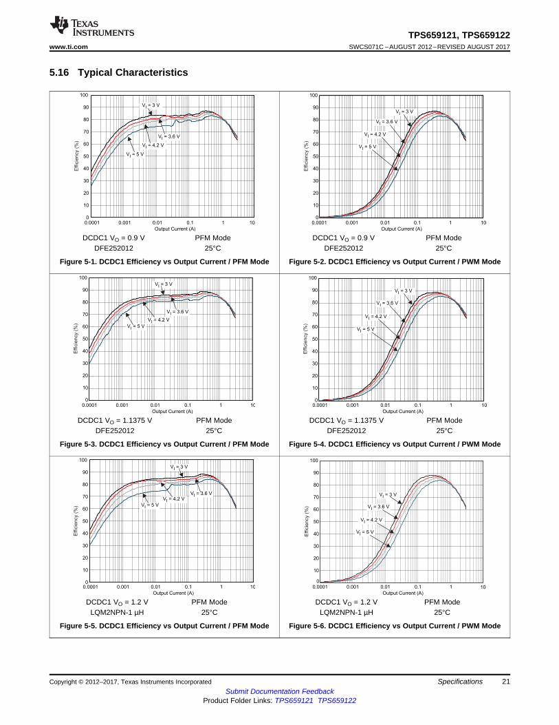
5.16 Typical Characteristics
DCDC1 VO = 0.9 V PFM ModeDFE252012 25°C
Figure 5-1. DCDC1 Efficiency vs Output Current / PFM Mode
DCDC1 VO = 0.9 V PFM ModeDFE252012 25°C
Figure 5-2. DCDC1 Efficiency vs Output Current / PWM Mode
DCDC1 VO = 1.1375 V PFM ModeDFE252012 25°C
Figure 5-3. DCDC1 Efficiency vs Output Current / PFM Mode
DCDC1 VO = 1.1375 V PFM ModeDFE252012 25°C
Figure 5-4. DCDC1 Efficiency vs Output Current / PWM Mode
DCDC1 VO = 1.2 V PFM ModeLQM2NPN-1 µH 25°C
Figure 5-5. DCDC1 Efficiency vs Output Current / PFM Mode
DCDC1 VO = 1.2 V PFM ModeLQM2NPN-1 µH 25°C
Figure 5-6. DCDC1 Efficiency vs Output Current / PWM Mode
0
10
20
30
40
50
60
70
80
90
100
Effic
iency (
%)
0.0001 0.001 0.01 0.1 1 10
Output Current (A)
V = 3 VI
V = 3.6 VIV = 4.2 VI
V = 5 VI
0
10
20
30
40
50
60
70
80
90
100
Effic
iency (
%)
0.0001 0.001 0.01 0.1 1 10
Output Current (A)
V = 3 VI
V = 3.6 VI
V = 4.2 VI
V = 5 VI
0
10
20
30
40
50
60
70
80
90
100
Effic
iency (
%)
0.0001 0.001 0.01 0.1 1 10
Output Current (A)
V = 3 VI
V = 3.6 VI
V = 4.2 VI
V = 5 VI
0
10
20
30
40
50
60
70
80
90
100
Effic
iency (
%)
0.0001 0.001 0.01 0.1 1 10
Output Current (A)
V = 3 VIV = 3.6 VIV = 4.2 VI
V = 5 VI
0.0001 0.001 0.01 0.1 1 10
Output Current (A
0
10
20
30
40
50
60
70
80
90
100
Effic
iency (
%)
V = 3 VIV = 3.6 VI
V = 4.2 VI
V = 5 VI
0.0001 0.001 0.01 0.1 1 10
Output Current (A)
0
10
20
30
40
50
60
70
80
90
100
Effic
iency (%
)
V = 3 VI
V = 3.6 VI
V = 4.2 VI
V = 5 VI
22
TPS659121, TPS659122SWCS071C –AUGUST 2012–REVISED AUGUST 2017 www.ti.com
Submit Documentation FeedbackProduct Folder Links: TPS659121 TPS659122
Specifications Copyright © 2012–2017, Texas Instruments Incorporated
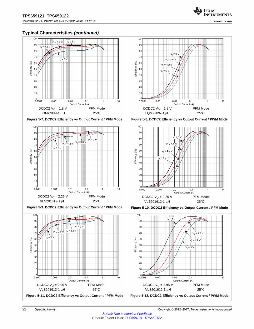
Typical Characteristics (continued)
DCDC2 VO = 1.8 V PFM ModeLQM2NPN-1 µH 25°C
Figure 5-7. DCDC2 Efficiency vs Output Current / PFM Mode
DCDC2 VO = 1.8 V PFM ModeLQM2NPN-1 µH 25°C
Figure 5-8. DCDC2 Efficiency vs Output Current / PWM Mode
DCDC2 VO = 2.25 V PFM ModeVLS201612-1 µH 25°C
Figure 5-9. DCDC2 Efficiency vs Output Current / PFM Mode
DCDC2 VO = 2.25 V PFM ModeVLS201612-1 µH 25°C
Figure 5-10. DCDC2 Efficiency vs Output Current / PFM Mode
DCDC2 VO = 2.95 V PFM ModeVLS201612-1 µH 25°C
Figure 5-11. DCDC2 Efficiency vs Output Current / PFM Mode
DCDC2 VO = 2.95 V PFM ModeVLS201612-1 µH 25°C
Figure 5-12. DCDC2 Efficiency vs Output Current / PWM Mode
0.0001 0.001 0.01 0.1 1 10
Output Current (A)
0
10
20
30
40
50
60
70
80
90
100
Effic
iency (
%)
V = 4.2 VI
V = 5 VI
0.0001 0.001 0.01 0.1 1 10
Output Current (A)
0
10
20
30
40
50
60
70
80
90
100
Effic
iency (
%)
V = 4.2 VI
V = 5 VI
0.0001 0.001 0.01 0.1 1 10
Output Current (A)
0
10
20
30
40
50
60
70
80
90
100
Effic
ien
cy (
%)
V = 3 VI
V = 3.6 VIV = 4.2 VIV = 5 VI
0.0001 0.001 0.01 0.1 1 10
Output Current (A)
0
10
20
30
40
50
60
70
80
90
100
Effic
iency (
%)
V = 3 VI
V = 3.6 VI
V = 4.2 VI
V = 5 VI
0.0001 0.001 0.01 0.1 1 10
Output Current (A)
0
10
20
30
40
50
60
70
80
90
100
Effic
iency (
%)
V = 3 VI
V = 3.6 VI
V = 4.2 VI
V = 5 VI
0.0001 0.001 0.01 0.1 1 10
Output Current (A)
0
10
20
30
40
50
60
70
80
90
100
Effic
ien
cy (
%)
V = 3 VIV = 3.6 VIV = 4.2 VI
V = 5 VI
23
TPS659121, TPS659122www.ti.com SWCS071C –AUGUST 2012–REVISED AUGUST 2017
Submit Documentation FeedbackProduct Folder Links: TPS659121 TPS659122
SpecificationsCopyright © 2012–2017, Texas Instruments Incorporated
Typical Characteristics (continued)
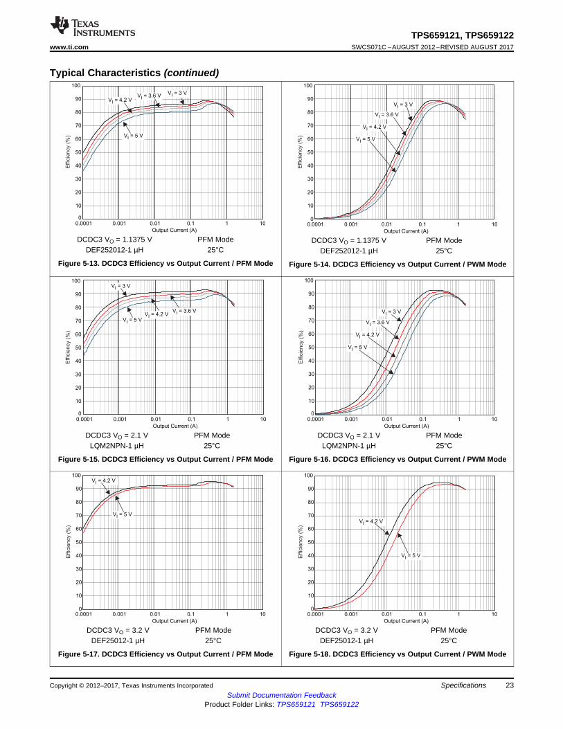
DCDC3 VO = 1.1375 V PFM ModeDEF252012-1 µH 25°C
Figure 5-13. DCDC3 Efficiency vs Output Current / PFM Mode
DCDC3 VO = 1.1375 V PFM ModeDEF252012-1 µH 25°C
Figure 5-14. DCDC3 Efficiency vs Output Current / PWM Mode
DCDC3 VO = 2.1 V PFM ModeLQM2NPN-1 µH 25°C
Figure 5-15. DCDC3 Efficiency vs Output Current / PFM Mode
DCDC3 VO = 2.1 V PFM ModeLQM2NPN-1 µH 25°C
Figure 5-16. DCDC3 Efficiency vs Output Current / PWM Mode
DCDC3 VO = 3.2 V PFM ModeDEF25012-1 µH 25°C
Figure 5-17. DCDC3 Efficiency vs Output Current / PFM Mode
DCDC3 VO = 3.2 V PFM ModeDEF25012-1 µH 25°C
Figure 5-18. DCDC3 Efficiency vs Output Current / PWM Mode
0
10
20
30
40
50
60
70
80
90
100
10 100 1k 10k 100k 1M 10M
Frequency (Hz)
Po
we
r S
up
ply
Re
jectio
n R
atio
(d
B)
10 100 1k 10k 100k 1M 10M
Frequency (Hz)
0
10
20
30
40
50
60
70
80
90
100
Po
we
r S
up
ply
Re
jectio
n R
atio
(d
B)
V _LDO = 1.8 V, V = 1.2 V, I = 10 mAIN OUT OUT
V _LDO = 1.8 V, V = 1.2 V, I = 100 mAIN OUT OUT
0.0001 0.001 0.01 0.1 1 10
Output Current (A)
0
10
20
30
40
50
60
70
80
90
100
Effic
iency (
%)
V = 3.8 VIV = 4.2 VI
V = 5 VI
0.0001 0.001 0.01 0.1 1 10
Output Current (A)
0
10
20
30
40
50
60
70
80
90
100
Effic
ien
cy (
%)
V = 3.8 VI
V = 4.2 VI
V = 5 VI
V = 3 VI
V = 3.6 VI
V = 4.2 VI
V = 5 VI
0.0001 0.001 0.01 0.1 1 10
Output Current (A)
0
10
20
30
40
50
60
70
80
90
100
Effic
iency (
%)
V = 3 VI
V = 3.6 VI
V = 4.2 VI
V = 5 VI
0.0001 0.001 0.01 0.1 1 10
Output Current (A)
0
10
20
30
40
50
60
70
80
90
100
Effic
iency (
%)
24
TPS659121, TPS659122SWCS071C –AUGUST 2012–REVISED AUGUST 2017 www.ti.com
Submit Documentation FeedbackProduct Folder Links: TPS659121 TPS659122
Specifications Copyright © 2012–2017, Texas Instruments Incorporated
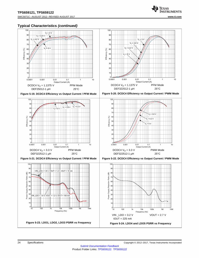
Typical Characteristics (continued)
DCDC4 VO = 1.1375 V PFM ModeDEF25012-1 µH 25°C
Figure 5-19. DCDC4 Efficiency vs Output Current / PFM Mode
DCDC4 VO = 1.1375 V PFM ModeDEF322512-1 µH 25°C
Figure 5-20. DCDC4 Efficiency vs Output Current / PWM Mode
DCDC4 VO = 3.3 V PFM ModeDEF322512-1 µH 25°C
Figure 5-21. DCDC4 Efficiency vs Output Current / PFM Mode
DCDC4 VO = 3.3 V PWM ModeDEF322512-1 µH 25°C
Figure 5-22. DCDC4 Efficiency vs Output Current / PWM Mode
Figure 5-23. LDO1, LDO2, LDO3 PSRR vs Frequency
VIN _LDO = 3.2 V VOUT = 2.7 VIOUT = 225 mA
Figure 5-24. LDO4 and LDO5 PSRR vs Frequency
10 100 1k 10k 100k 1M 10M
Frequency (Hz)
0
10
20
30
40
50
60
70
80
90
100
Po
we
r S
up
ply
Re
jectio
n R
atio
(d
B)
V _LDO9 = 3.3 V, V = 2.85 V, I = 10 mAIN OUT OUT
V _LDO9 = 3.3 V, V = 2.85 V, I = 300 mAIN OUT OUT
10 100 1k 10k 100k 1M 10M
Frequency (Hz
0
10
20
30
40
50
60
70
80
90
100
Po
we
r S
up
ply
Re
jectio
n R
atio
(d
B)
V _LDO = 5 V, V = 3.3 V, I = 10 mAIN OUT OUT
V _LDO = 5 V, V = 3.3 V, I = 100 mAIN OUT OUT
0
10
20
30
40
50
60
70
80
90
100
10 100 1k 10k 100k 1M 10M
Frequency (Hz)
V _LDO = 3.3 V, V = 1.8 V, I = 10 mAIN OUT OUT
VIN_LDO = 3.3 V, VOUT = 1.8 V, IOUT = 100 mA
VIN_LDO = 3.3 V, VOUT = 2.85 V, IOUT = 10 mA
VIN_LDO = 3.3 V, VOUT = 2.85 V, IOUT = 100 mA
Pow
er
Supply
Reje
ction R
atio (
dB
)
25
TPS659121, TPS659122www.ti.com SWCS071C –AUGUST 2012–REVISED AUGUST 2017
Submit Documentation FeedbackProduct Folder Links: TPS659121 TPS659122
SpecificationsCopyright © 2012–2017, Texas Instruments Incorporated
Typical Characteristics (continued)
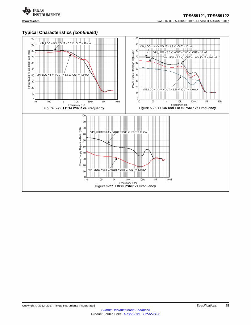
Figure 5-25. LDO4 PSRR vs Frequency Figure 5-26. LDO6 and LDO8 PSRR vs Frequency
Figure 5-27. LDO9 PSRR vs Frequency
Sr PSr
tfDA trDA
thd;DAT
tsu;STA thd;STA tsu;DAT
tsu;STO
trCL1
tfCL
tHIGH tLOW tLOW tHIGH
trCLtrCL1
= MCS Current Source Pull-Up
= R(P) Resistor Pull-Up
SDAH
SCLH
See Note ASee Note A
SDA
SCL
tftf
trtr
tLOW
thd;STA
thd;DAT HIGH
tsu;DAT
tsu;STA
thd;STA
tsu;STO
tBUF
S Sr P S
26
TPS659121, TPS659122SWCS071C –AUGUST 2012–REVISED AUGUST 2017 www.ti.com
Submit Documentation FeedbackProduct Folder Links: TPS659121 TPS659122
Parameter Measurement Information Copyright © 2012–2017, Texas Instruments Incorporated
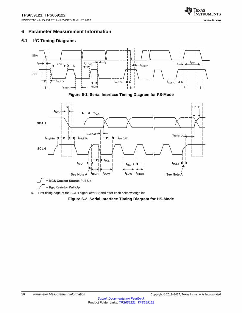
6 Parameter Measurement Information
6.1 I2C Timing Diagrams
Figure 6-1. Serial Interface Timing Diagram for FS-Mode
A. First rising edge of the SCLH signal after Sr and after each acknowledge bit.
Figure 6-2. Serial Interface Timing Diagram for HS-Mode
R/W Address 8 bits unused bits (7 bits) Data (8 bits)
ERROR (15 bits)
SPI C h ip S e lect
SPI C lock E nab le
SPI D ata I nput
SP I D ata O utput
tckper
t cklowtcesu
t sisu
t sihld
tcehld
t dr
tckhigh
27
TPS659121, TPS659122www.ti.com SWCS071C –AUGUST 2012–REVISED AUGUST 2017
Submit Documentation FeedbackProduct Folder Links: TPS659121 TPS659122
Parameter Measurement InformationCopyright © 2012–2017, Texas Instruments Incorporated
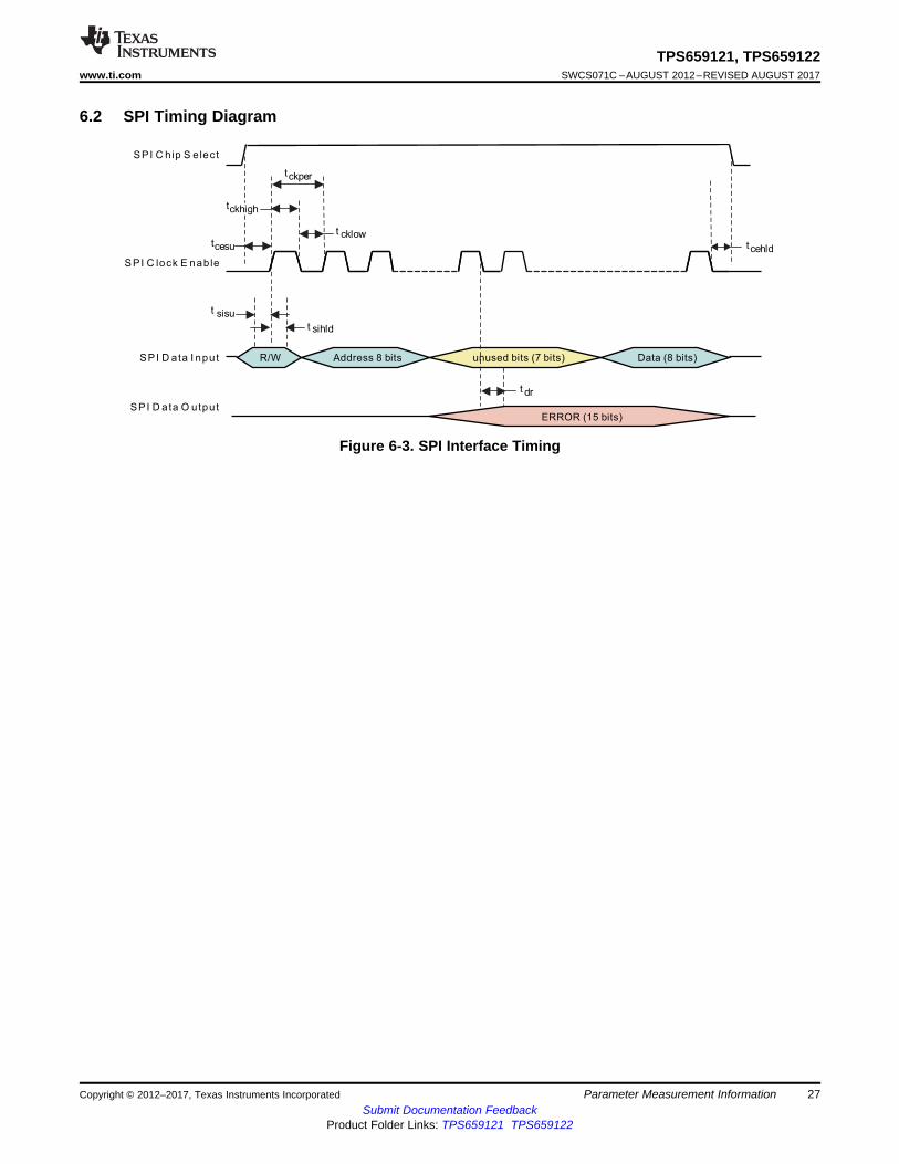
6.2 SPI Timing Diagram
Figure 6-3. SPI Interface Timing
28
TPS659121, TPS659122SWCS071C –AUGUST 2012–REVISED AUGUST 2017 www.ti.com
Submit Documentation FeedbackProduct Folder Links: TPS659121 TPS659122
Detailed Description Copyright © 2012–2017, Texas Instruments Incorporated
7 Detailed Description
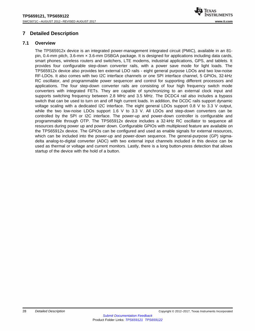
7.1 OverviewThe TPS65912x device is an integrated power-management integrated circuit (PMIC), available in an 81-pin, 0.4-mm pitch, 3.6-mm × 3.6-mm DSBGA package. It is designed for applications including data cards,smart phones, wireless routers and switchers, LTE modems, industrial applications, GPS, and tablets. Itprovides four configurable step-down converter rails, with a power save mode for light loads. TheTPS65912x device also provides ten external LDO rails - eight general purpose LDOs and two low-noiseRF-LDOs. It also comes with two I2C interface channels or one SPI interface channel, 5 GPIOs, 32-kHzRC oscillator, and programmable power sequencer and control for supporting different processors andapplications. The four step-down converter rails are consisting of four high frequency switch modeconverters with integrated FETs. They are capable of synchronizing to an external clock input andsupports switching frequency between 2.8 MHz and 3.5 MHz. The DCDC4 rail also includes a bypassswitch that can be used to turn on and off high current loads. In addition, the DCDC rails support dynamicvoltage scaling with a dedicated I2C interface. The eight general LDOs support 0.8 V to 3.3 V output,while the two low-noise LDOs support 1.6 V to 3.3 V. All LDOs and step-down converters can becontrolled by the SPI or I2C interface. The power-up and power-down controller is configurable andprogrammable through OTP. The TPS65912x device includes a 32-kHz RC oscillator to sequence allresources during power up and power down. Configurable GPIOs with multiplexed feature are available onthe TPS65912x device. The GPIOs can be configured and used as enable signals for external resources,which can be included into the power-up and power-down sequence. The general-purpose (GP) sigma-delta analog-to-digital converter (ADC) with two external input channels included in this device can beused as thermal or voltage and current monitors. Lastly, there is a long button-press detection that allowsstartup of the device with the hold of a button.
VBat
VBat
VBat
SDA_MOSI
SCL_CLK
VINLDO3
LDO3
VDDIO
SW4DCDC4
2.5 A VDCDC4
VINDCDC4
AGND
VREF1V25
PGND4
SW3
VDCDC3
PGND3
SW2
VINDCDC2
10 µF
PGND2
GPIO2_CE
GPIO1_MISO
I2C/SPI
nPWRON (nRESIN)
nRESPWRON
INT1
SLEEP (PWR_REQ)
PWRHOLD
DGND
VINLDO1210
LDO1LDO1
(0.8-3.3 V, 50 mV step
@100 mA)LDO2
LDO2(0.8-3.3 V, 50 mV step
@100 mA)VINLDO4
LDO4LDO4(1.6-3.3 V, 50 mV step
@250 mA)Low noise
LDO5
LDO6
VINLDO5
LDO7LDO7
(0.8-3.3 V, 50 mV step@200 mA)
LDO8
LDO9LDO9(0.8-3.3 V, 50 mV step
@300 mA)
RGBLED
BIAS
PowerControl
TPS65912x
32 kHzRC
OSC
ON/OFF
Vth
+
-
SDA_AVS (CLK_REQ2)
SCL_AVS (CLK_REQ1)
EN1 (DCDC1_SEL)
EN2 (DCDC2_SEL)
VINLDO67
LDO5(1.6-3.3 V, 50 mV
step @250 mA)Low noise
LDO6(0.8-3.3 V, 50 mV step
@100 mA)
LDO3(0.8-3.3 V, 50 mV step
@100 mA)
LDO8(0.8-3.3 V, 50 mV step
@100 mA)
EN3 (DCDC3_SEL)
EN4 (DCDC4_SEL)
Thermal
warning and
shutdown
LDOAOInternal
LDO
LEDA/GPIO3
LEDB/GPIO4
LEDC/GPIO5
LDO10LDO10(0.8-3.3 V, 50 mV step
@300 mA)
VINLDO
1210
Load Switch
LSI
LSO
L4
L3
L2
CoutDCDC4
CoutDCDC3
CoutDCDC3
CIN4
CIN3
CIN2
VDCDC4_GND
VBat
SW1
VDCDC1
VINDCDC1
PGND1
L1
CoutDCDC1
CIN1
VDCDC1_GND
VINDCDC3
VDCDC2
CoutLDO3
CoutLDO2
CoutLDO1
CoutLDO4
CoutLDO5
CoutLDO6
CoutLDO7
CoutLDO8
CoutLDO9
CoutLDO10
CinLDO67
CinLDO5
CinLDO4
CinLDO1210
CinLDO3
VINLDO8
CinLDO8
VINLDO9
CinLDO9
VCON_PWM
VCON_CLK
OMAP_WDI (32k_OUT)
CONFIG1
CONFIG2
VIN_DCDC_ANA
DEF_SPI_I2C-GPIO
VCC
CPCAP_WDI
AGND
EN_LS0
EN_LS1
CVIN_DCDC_ANA
CVCC
VCCS_VIN_MON
tie to GND
or LDOAO
10 µF
1 µH
1 µH
10 µF
10 µF
1 µH
1 µH
DCDC1
2.5 A
DCDC3
1.6 A
DCDC2
0.75 A
100 nF
29
TPS659121, TPS659122www.ti.com SWCS071C –AUGUST 2012–REVISED AUGUST 2017
Submit Documentation FeedbackProduct Folder Links: TPS659121 TPS659122
Detailed DescriptionCopyright © 2012–2017, Texas Instruments Incorporated
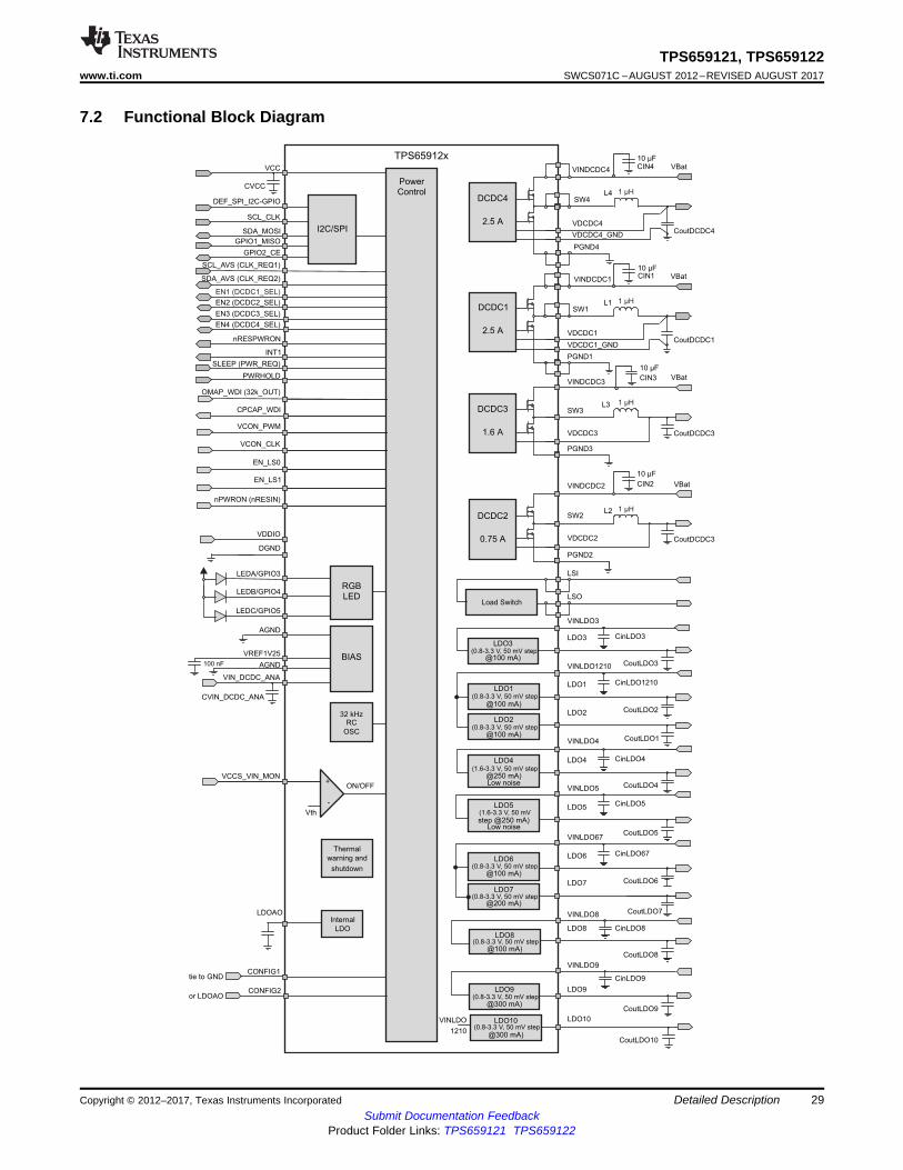
7.2 Functional Block Diagram
30
TPS659121, TPS659122SWCS071C –AUGUST 2012–REVISED AUGUST 2017 www.ti.com
Submit Documentation FeedbackProduct Folder Links: TPS659121 TPS659122
Detailed Description Copyright © 2012–2017, Texas Instruments Incorporated
7.3 Linear RegulatorsThe power management core has 10 LDOs with various output voltage/current capabilities. Each LDOoutput voltage can be set independently through the communication bus (see LDO Voltage Settings tablein Section 7.28.2) and the transition occurs immediately if the LDO is enabled.
7.3.1 Low Quiescent Current Mode (Eco-mode™)Each LDO is equipped with a low quiescent current mode that can enabled or disabled separately. Whenthe ECO bit is 1, the LDOx Eco-mode™ control scheme is enabled.
7.3.2 Output DischargeEach LDO is equipped with an output discharge bit. When the bit is set to 1, the output of the LDO will bedischarged to ground with the equivalent of a 300-Ω resistor. If the LDO is enabled, the discharge bit isignored.
7.3.3 Thermal ShutdownThere is a global thermal shutdown protection for all step-down converters and LDOs. The thermal sensorwill generate an early warning depending on the setting of register THRM_REG. If the temperature risesabove the thermal shutdown threshold, the complete device is powered down to OFF state.
7.3.4 LDO EnableThe LDOs enable/disable is part of the flexible power-up and power-down state machine. Each LDO canbe programmed such that it is powered up automatically in one of the 15 time slots after a power-oncondition occurs or is controlled by a dedicated pin. Pins EN_1, EN_2, EN_3 and EN_4 as well as pinsCLK_REQ1, CLK_REQ2 and PWR_REQ (SLEEP) can be mapped to any resource (LDOs, DC-DCconverter, 32-kHz clock output or GPIO) to enable or disable it.
7.3.5 LDO Voltage RangeThe output voltage range for the standard LDOs is 0.8 V to 3.3 V. For the RF-LDOs, LDO4 and LDO5, theoutput voltage range is 1.6 V to 3.3 V. The most significant bit for the voltage settings SEL[5] on LDO4and LDO5 is ignored and is internally set to 1.
7.3.6 LDO Power Good ComparatorThe output voltage of each LDO is supervised by an internal power good comparator. Its output is settingand clearing the PGOOD bits in registers PGOOD and PGOOD2. The power good bits are not valid if theLDO is enabled but the input voltage to the LDO is below 1 V.
31
TPS659121, TPS659122www.ti.com SWCS071C –AUGUST 2012–REVISED AUGUST 2017
Submit Documentation FeedbackProduct Folder Links: TPS659121 TPS659122
Detailed DescriptionCopyright © 2012–2017, Texas Instruments Incorporated
7.4 Step-Down ConvertersThe synchronous step-down converter used in the power management core includes a unique hystericPWM controller scheme which enables switch frequencies over 3 MHz, excellent transient and AC loadregulation as well as operation with tiny and cost competitive external components.
The controller topology supports forced PWM Mode as well as Power Save Mode operation. Power SaveMode operation reduces the quiescent current consumption and ensures high conversion efficiency at lightloads by skipping switch pulses.
A significant advantage of this architecture compared to other hysteretic PWM controller topologies is itsexcellent DC and AC load regulation capability in combination with low output voltage ripple over theentire load range which makes this part well suited for audio and RF applications.
Once the output voltage falls below the threshold of the error comparator a switch pulse is initiated andthe high side switch is turned on. It remains turned on until a minimum on time of TONmin expires and theoutput voltage trips the threshold of the error comparator or the inductor current reaches the high sideswitch current limit. Once the high side switch turns off, the low side switch rectifier is turned on and theinductor current ramps down until the high side switch turns on again or the inductor current reaches zero.
7.4.1 PWM/PFM ModeIn forced PWM Mode, the device avoids pulse skipping and allows easy filtering of the switch noise byexternal filter components. PWM mode is forced by setting bit DCDCx_MODE = 1. If this bit is not set, theDCDC outputs will switch to a low current PFM mode when there is light load and sufficient headroombetween the DCDCx input and output rails.
7.4.2 Low Quiescent Current ModeEach step-down converter may be individually controlled to enter a low quiescent current mode. Thismode is entered when the ECO bit is 1. In ECO mode, the quiescent current is reduced and the outputvoltage is supervised by a comparator while most part of the control is disabled to save power. ECO modeshould only be enabled when a converter has less than 2 mA of load current. In addition, the ECO modeshould be disabled prior to a load transient step to allow the converter to respond in a timely manner tothe excess current draw. Setting the step-down converter into PWM mode by DCDCx_MODE = 1 disablesECO mode independently from the setting of bit ECO.
7.4.3 Output Voltage MonitoringInternal power good comparators monitors the switching regulator outputs and detect when the outputvoltage is below 90% of the programmed value. This information is used by the power management coreto generate interrupts depending on specific I2C register settings. See the Interrupt Controller section foradditional details. An individual power good comparator of the switching regulator will be blanked whenthe regulator is disabled or when the voltage of the regulator is transitioning from one set point to another.
7.4.4 Output DischargeEach switching regulator is equipped with an output discharge enable bit. When the bit is set to 1, theoutput of the regulator will be discharged to ground with the equivalent of a 400-Ω resistor. If the enablebit of the regulator is set, the discharge bit is ignored.
7.4.5 Thermal ShutdownThere is a global thermal shutdown protection for all step-down converters and LDOs. The thermal sensorwill generate an early warning depending on the setting of register THRM_REG. If the temperature risesabove the thermal shutdown threshold, the complete device is powered down to OFF state.
EN
95%
5%
VOUT
tStart
tRAMP
32
TPS659121, TPS659122SWCS071C –AUGUST 2012–REVISED AUGUST 2017 www.ti.com
Submit Documentation FeedbackProduct Folder Links: TPS659121 TPS659122
Detailed Description Copyright © 2012–2017, Texas Instruments Incorporated
7.4.6 Step-Down Converter ENABLEThe step-down converter enable/disable is part of the flexible power-up and power-down state machine.Each converter can be programmed such that it is powered up automatically in one of the 15 time slotsafter a power-on condition occurs or is controlled by a dedicated pin. Pins EN_1, EN_2, EN_3 and EN_4as well as pins CLK_REQ1, CLK_REQ2 and PWR_REQ (SLEEP) can be mapped to any resource (LDOs,DC-DC converter, 32 kHz clock output or GPIO) to enable or disable it.
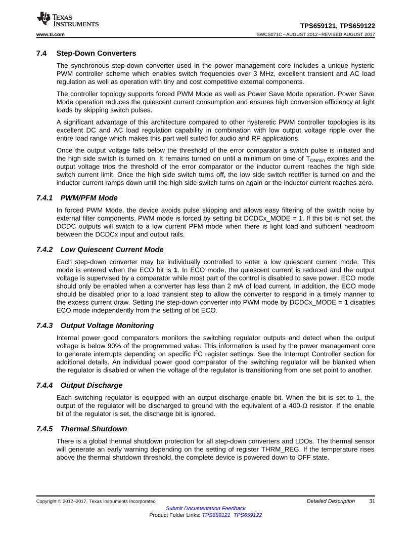
7.4.7 Step-Down converter SOFT STARTThe step-down converters in TPS65912x have an internal soft-start circuit that controls the ramp up of theoutput voltage. The output voltage ramps up from 5% to 95% of its nominal value within a time defined inSection 5. This limits the inrush current in the converter during start up and prevents possible input voltagedrops when a battery or high impedance power source is used. The soft-start circuit is enabled after thestart-up time tStart has expired. For DCDC4, there is an option to set two different values for the start upand ramp time. For applications that require a fast response, set DCDC4_CTRL:RAMP_TIME = 1.
During soft start, the output voltage ramp up is controlled as shown in Figure 7-1.
Figure 7-1. Soft Start
The step-down converter enable/disable is part of the flexible power-up and power-down state machine.Each converter can be programmed such that it is powered up automatically in one of the 15 time slotsafter a power-on condition occurs or is controlled by a dedicated pin. Pins EN_1, EN_2, EN_3 and EN_4as well as pins CLK_REQ1, CLK_REQ2 and PWR_REQ (SLEEP) can be mapped to any resource (LDOs,DC-DC converter, 32 kHz clock output or GPIO) to enable or disable it.
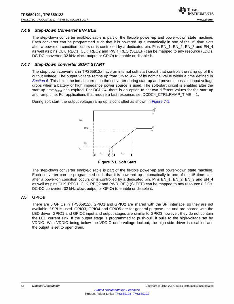
7.5 GPIOsThere are 5 GPIOs in TPS65912x. GPIO1 and GPIO2 are shared with the SPI interface, so they are notavailable if SPI is used. GPIO3, GPIO4 and GPIO5 are for general purpose use and are shared with theLED driver. GPIO1 and GPIO2 input and output stages are similar to GPIO3 however, they do not containthe LED current sink. If the output stage is programmed to push-pull, it pulls to the high-voltage set byVDDIO. With VDDIO being below the VDDIO undervoltage lockout, the high-side driver is disabled andthe output is set to open drain.
open drain enableGPIO_ODEN
output enableGPIO_CFG
DATA OUT
VDDIO
LED_PWM
DATA IN
GPIOx /LEDx
LEDcurrent
sink
backgate
switch
pull-down enableGPIO_PDEN
4.7 k
33
TPS659121, TPS659122www.ti.com SWCS071C –AUGUST 2012–REVISED AUGUST 2017
Submit Documentation FeedbackProduct Folder Links: TPS659121 TPS659122
Detailed DescriptionCopyright © 2012–2017, Texas Instruments Incorporated
Figure 7-2. GPIO Block for GPIO3, GPIO4, and GPIO5
7.6 Power State MachineThe embedded power controller (EPC) manages the state of the device and controls the power upsequence.
The EPC will support the following states:
The transitions for the state machine are shown figure belowNO SUPPLY The main battery supply voltage is not high enough to power the LDOAO (LDO always ON)
regulator. A global reset is asserted in this case. Everything on the device is off.CONFIG This state is entered either from NO SUPPLY state automatically or from ACTIVE or SLEEP
when TPS65912x is configured accordingly by Bit LOAD-OTP in [DEVCTRL:Bit6]. WhenCONFIG is entered, all registers are set to their default value; nRESPWRON is asserted.
OFF LDOAO is on and internal logic is active. All power supplies are in off-state. Device candetect and execute power-up sequence. nRESPWRON is asserted.
ACTIVE Device POWER ON enable conditions are met and regulated power supplies are ON or canbe enabled with full current capability. Reset is released; interfaces are active.
SLEEP Device SLEEP enable conditions are met and selected regulated power supplies are in low-power/OFF mode.
7.7 Transition Conditions• Device POWER ON enable conditions:
– nPWRON signal low level– Or PWRHOLD signal high level– Or Pwr_hold_reg control bit set to 1 (default inactive)– Or interrupt flag active (default INT1 low) will generate a POWER ON enable condition during a
fixed delay (During this delay it is expected processor to main acknowledge power by writing inPwr_Hold reg or setting Power Hold pin to 1). Interrupt sources Generate wake up only if they arenot Mask (OTP/Register dependant)
• Device POWER ON disable conditions:– nPWRON signal low level during more than the Long Press delay: PWON_LP_DELAY (can be
disable though register programming). The interrupt corresponding to this condition is thePWRON_LP_IT in INT_STS_REG register.
– Or Die temperature has reached the thermal shutdown threshold (THERM_TS=1)– Or DEV_OFF_RST control bit set to 1
34
TPS659121, TPS659122SWCS071C –AUGUST 2012–REVISED AUGUST 2017 www.ti.com
Submit Documentation FeedbackProduct Folder Links: TPS659121 TPS659122
Detailed Description Copyright © 2012–2017, Texas Instruments Incorporated
• Device SLEEP enable condition:– SLEEP signal low level (Default, or high level depending of the programmed polarity)– AND DEV_SLP control bit set to 1– AND interrupt flag inactive (default INT1 high): no none masked interrupt pending
• Device has three different reset scenarios:– Full reset: all digital of device is reset
• Caused by POR (Power On Reset) when VCCS < UVLO– General reset:
• Caused by turn-off event with LOAD-OTP=1• Turn-off event by PWON_LP_OFF_RST bit set to 1• Optionally for TPS65912x1 by pin PWRON pulled low for longer than 100 ms
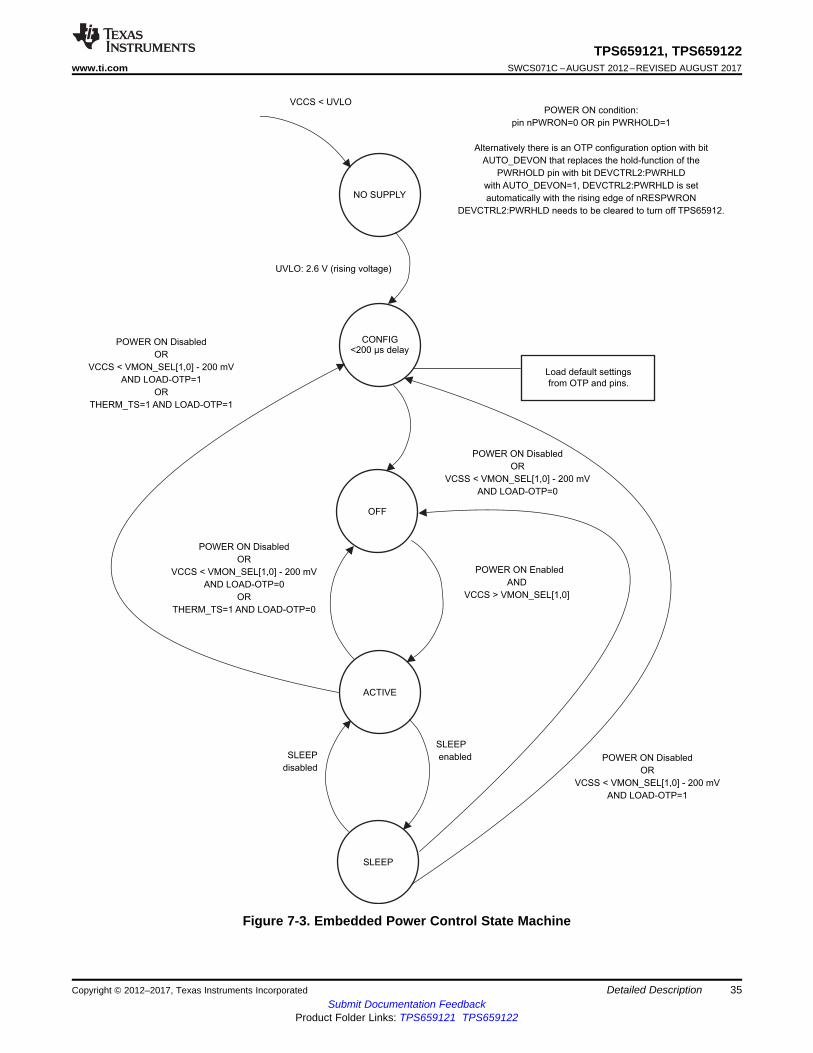
POWER ON Enabled
AND
VCCS > VMON_SEL[1,0]
SLEEP
enabledSLEEP
disabledPOWER ON Disabled
OR
VCSS < VMON_SEL[1,0] - 200 mV
AND LOAD-OTP=1
POWER ON Disabled
OR
VCCS <
AND LOAD-OTP=1
OR
THERM_TS=1 AND LOAD-OTP=1
VMON_SEL[1,0] - 200 mV
VCCS < UVLO
NO SUPPLY
OFF
ACTIVE
SLEEP
UVLO: 2.6 V (rising voltage)
Load default settings
from OTP and pins.
POWER ON Disabled
OR
VCCS <
AND LOAD-OTP=0
OR
VMON_SEL[1,0] - 200 mV
THERM_TS=1 AND LOAD-OTP=0
POWER ON Disabled
OR
VCSS < VMON_SEL[1,0] - 200 mV
AND LOAD-OTP=0
CONFIG<200 µs delay
POWER ON condition:
pin nPWRON=0 OR pin PWRHOLD=1
Alternatively there is an OTP configuration option with bit
AUTO_DEVON that replaces the hold-function of the
PWRHOLD pin with bit DEVCTRL2:PWRHLD
with AUTO_DEVON=1, DEVCTRL2:PWRHLD is set
automatically with the rising edge of nRESPWRON
DEVCTRL2:PWRHLD needs to be cleared to turn off TPS65912.
35
TPS659121, TPS659122www.ti.com SWCS071C –AUGUST 2012–REVISED AUGUST 2017
Submit Documentation FeedbackProduct Folder Links: TPS659121 TPS659122
Detailed DescriptionCopyright © 2012–2017, Texas Instruments Incorporated
Figure 7-3. Embedded Power Control State Machine
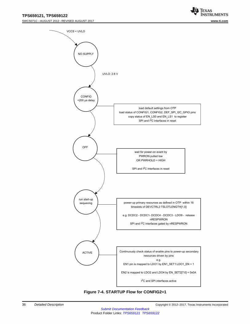
VCCS < UVLO
NO SUPPLY
OFF
ACTIVE
CONFIG
<200 µs delay
UVLO: 2.6 V
load default settings from OTP
load status of CONFIG1, CONFIG2, DEF_SPI_I2C_GPIO pins
copy status of EN_LS0 and EN_LS1 to register
SPI and I C interfaces in reset2
wait for power-on event by
PWRON pulled low
OR PWRHOLD = HIGH
SPI and interfaces in resetI C2
run start-up
sequecing power-up primary resources as defined in OTP within 16
timeslots of DEVCTRL2:TSLOTLENGTH[1,0]
e.g. DCDC2 - DCDC1- DCDC4 - DCDC3 - LDO9 - release
nRESPWRON
SPI and interfaces gated by nRESPWRONI C2
Continuously check status of enable pins to power-up secondary
resources driven by pins
e.g.
EN1 pin is mapped to LDO1 by EN1_SET1:LDO1_EN = 1
EN2 is mapped to LDO2 and LDO4 by EN_SET2[7:0] = 0x0A
and SPI interfaces activeI C2
36
TPS659121, TPS659122SWCS071C –AUGUST 2012–REVISED AUGUST 2017 www.ti.com
Submit Documentation FeedbackProduct Folder Links: TPS659121 TPS659122
Detailed Description Copyright © 2012–2017, Texas Instruments Incorporated
Figure 7-4. STARTUP Flow for CONFIG2=1
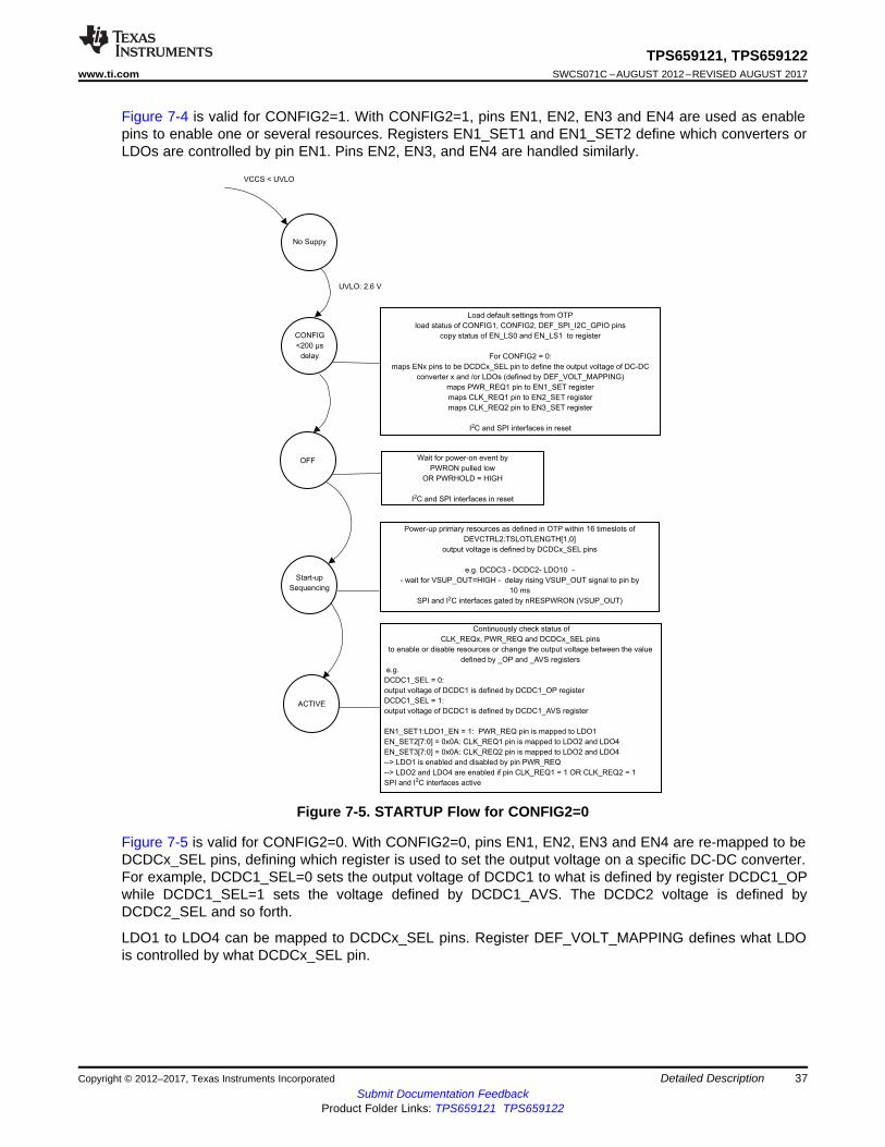
VCCS < UVLO
No Suppy
OFF
ACTIVE
CONFIG
<200 µs
delay
UVLO: 2.6 V
Load default settings from OTP
load status of CONFIG1, CONFIG2, DEF_SPI_I2C_GPIO pins
copy status of EN_LS0 and EN_LS1 to register
For CONFIG2 = 0:
maps ENx pins to be DCDCx_SEL pin to define the output voltage of DC-DC
converter x and /or LDOs (defined by DEF_VOLT_MAPPING)
maps PWR_REQ1 pin to EN1_SET register
maps CLK_REQ1 pin to EN2_SET register
maps CLK_REQ2 pin to EN3_SET register
I C and SPI interfaces in reset2
Wait for power-on event by
PWRON pulled low
OR PWRHOLD = HIGH
I C and SPI interfaces in reset2
Start-up
Sequencing
Power-up primary resources as defined in OTP within 16 timeslots of
DEVCTRL2:TSLOTLENGTH[1,0]
output voltage is defined by DCDCx_SEL pins
e.g. DCDC3 - DCDC2- LDO10 -
- wait for VSUP_OUT=HIGH - delay rising VSUP_OUT signal to pin by
10 ms
SPI and I C interfaces gated by nRESPWRON (VSUP_OUT)2
Continuously check status of
CLK_REQx, PWR_REQ and DCDCx_SEL pins
to enable or disable resources or change the output voltage between the value
defined by _OP and _AVS registers
e.g.
DCDC1_SEL = 0:
output voltage of DCDC1 is defined by DCDC1_OP register
DCDC1_SEL = 1:
output voltage of DCDC1 is defined by DCDC1_AVS register
EN1_SET1:LDO1_EN = 1: PWR_REQ pin is mapped to LDO1
EN_SET2[7:0] = 0x0A: CLK_REQ1 pin is mapped to LDO2 and LDO4
EN_SET3[7:0] = 0x0A: CLK_REQ2 pin is mapped to LDO2 and LDO4
--> LDO1 is enabled and disabled by pin PWR_REQ
--> LDO2 and LDO4 are enabled if pin CLK_REQ1 = 1 OR CLK_REQ2 = 1
SPI and I C interfaces active2
37
TPS659121, TPS659122www.ti.com SWCS071C –AUGUST 2012–REVISED AUGUST 2017
Submit Documentation FeedbackProduct Folder Links: TPS659121 TPS659122
Detailed DescriptionCopyright © 2012–2017, Texas Instruments Incorporated
Figure 7-4 is valid for CONFIG2=1. With CONFIG2=1, pins EN1, EN2, EN3 and EN4 are used as enablepins to enable one or several resources. Registers EN1_SET1 and EN1_SET2 define which converters orLDOs are controlled by pin EN1. Pins EN2, EN3, and EN4 are handled similarly.
Figure 7-5. STARTUP Flow for CONFIG2=0
Figure 7-5 is valid for CONFIG2=0. With CONFIG2=0, pins EN1, EN2, EN3 and EN4 are re-mapped to beDCDCx_SEL pins, defining which register is used to set the output voltage on a specific DC-DC converter.For example, DCDC1_SEL=0 sets the output voltage of DCDC1 to what is defined by register DCDC1_OPwhile DCDC1_SEL=1 sets the voltage defined by DCDC1_AVS. The DCDC2 voltage is defined byDCDC2_SEL and so forth.
LDO1 to LDO4 can be mapped to DCDCx_SEL pins. Register DEF_VOLT_MAPPING defines what LDOis controlled by what DCDCx_SEL pin.
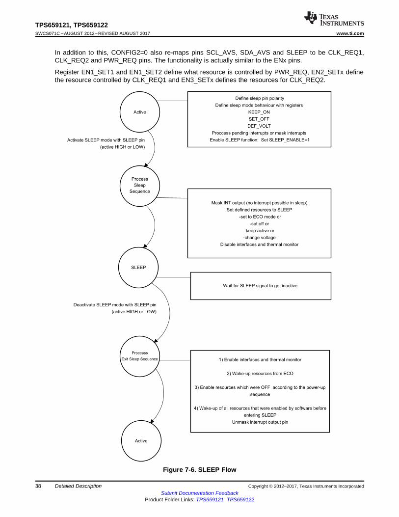
SLEEP
Active
Mask INT output (no interrupt possible in sleep)
Set defined resources to SLEEP
-set to ECO mode or
-set off or
-keep active or
-change voltage
Disable interfaces and thermal monitor
Wait for SLEEP signal to get inactive.
Proccess
Exit Sleep Sequence 1) Enable interfaces and thermal monitor
2) Wake-up resources from ECO
3) Enable resources which were OFF according to the power-up
sequence
4) Wake-up of all resources that were enabled by software before
entering SLEEP
Unmask interrupt output pin
Define sleep pin polarity
Define sleep mode behaviour with registers
KEEP_ON
SET_OFF
DEF_VOLT
Proccess pending interrupts or mask interrupts
Enable SLEEP function: Set SLEEP_ENABLE=1
Process
Sleep
Sequence
Activate SLEEP mode with SLEEP pin
(active HIGH or LOW)
Deactivate SLEEP mode with SLEEP pin
(active HIGH or LOW)
Active
38
TPS659121, TPS659122SWCS071C –AUGUST 2012–REVISED AUGUST 2017 www.ti.com
Submit Documentation FeedbackProduct Folder Links: TPS659121 TPS659122
Detailed Description Copyright © 2012–2017, Texas Instruments Incorporated
In addition to this, CONFIG2=0 also re-maps pins SCL_AVS, SDA_AVS and SLEEP to be CLK_REQ1,CLK_REQ2 and PWR_REQ pins. The functionality is actually similar to the ENx pins.
Register EN1_SET1 and EN1_SET2 define what resource is controlled by PWR_REQ, EN2_SETx definethe resource controlled by CLK_REQ1 and EN3_SETx defines the resources for CLK_REQ2.
Figure 7-6. SLEEP Flow
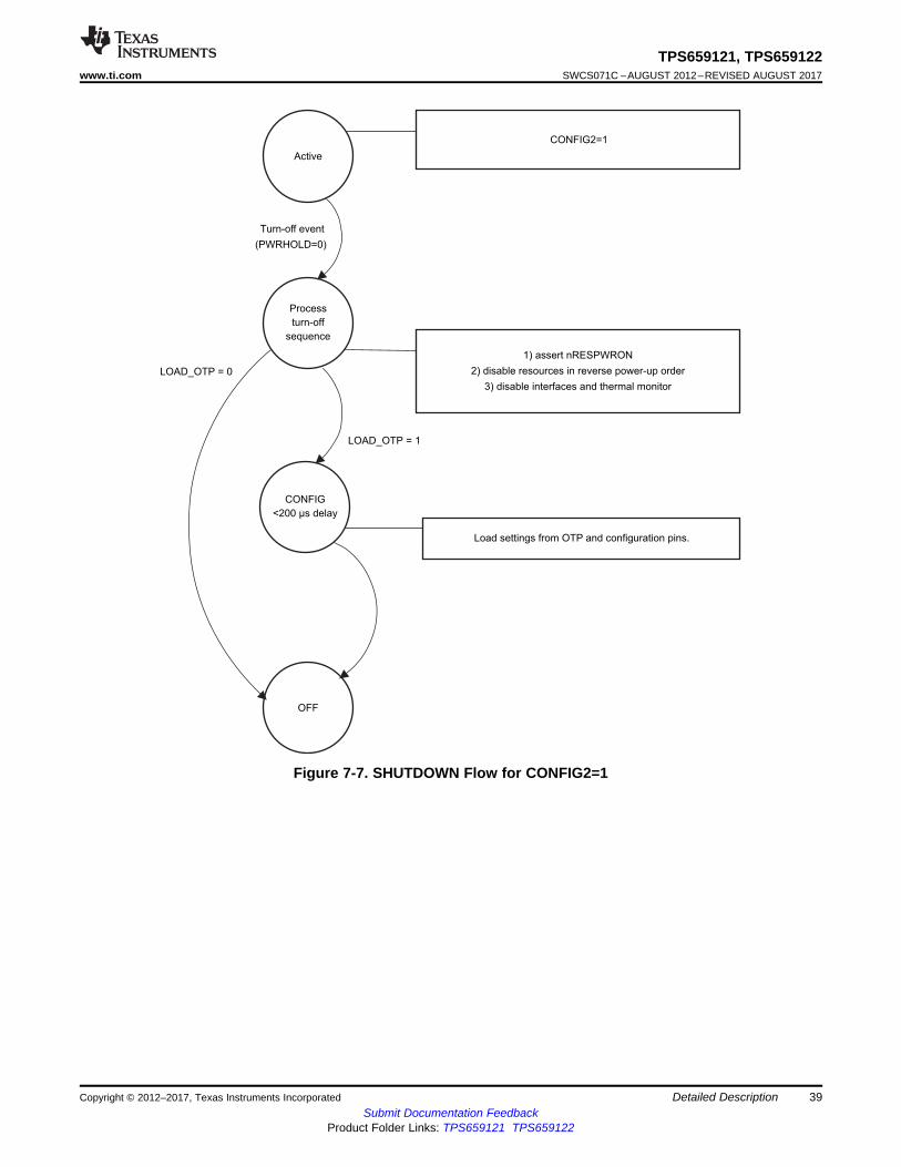
CONFIG
<200 µs delay
Active
1) assert nRESPWRON
2) disable resources in reverse power-up order
3) disable interfaces and thermal monitor
Load settings from OTP and configuration pins.
OFF
CONFIG2=1
Process
turn-off
sequence
Turn-off event
(PWRHOLD=0)
LOAD_OTP = 1
LOAD_OTP = 0
39
TPS659121, TPS659122www.ti.com SWCS071C –AUGUST 2012–REVISED AUGUST 2017
Submit Documentation FeedbackProduct Folder Links: TPS659121 TPS659122
Detailed DescriptionCopyright © 2012–2017, Texas Instruments Incorporated
Figure 7-7. SHUTDOWN Flow for CONFIG2=1
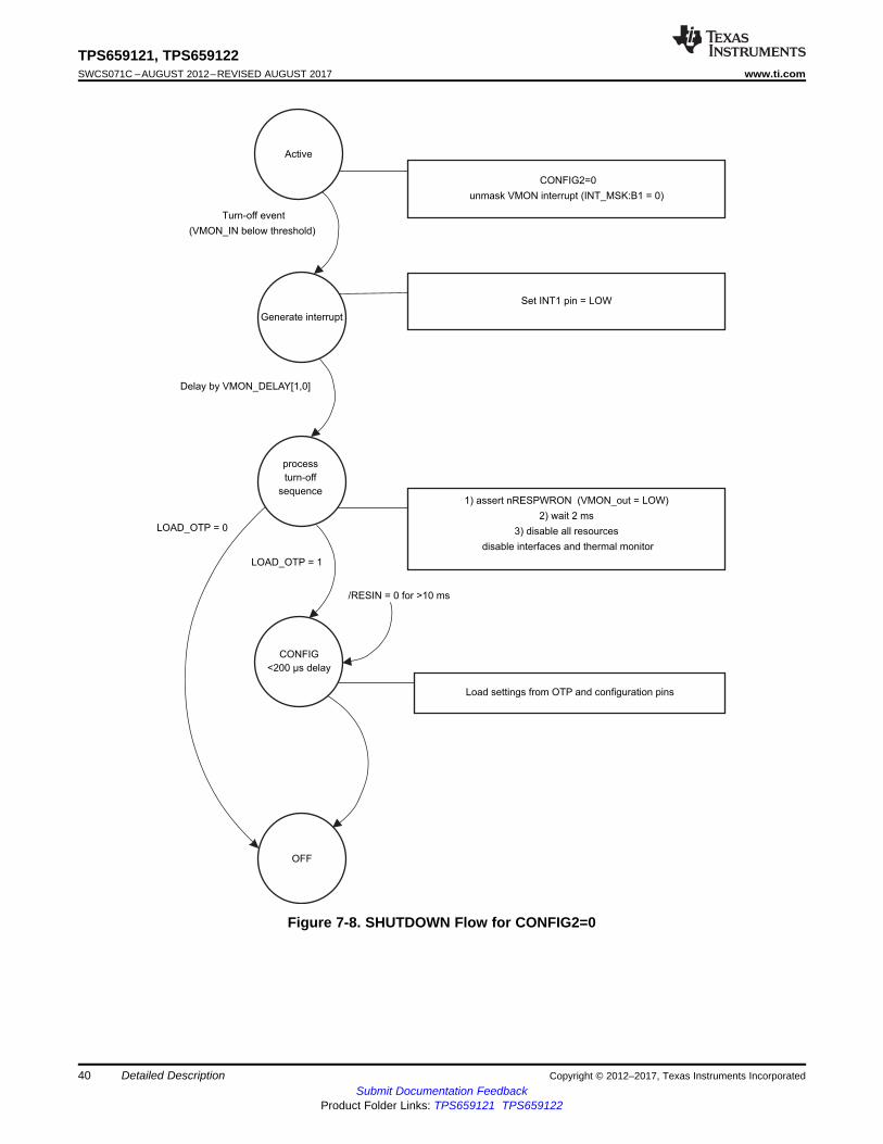
CONFIG
<200 µs delay
Generate interrupt
1) assert nRESPWRON (VMON_out = LOW)
2) wait 2 ms
3) disable all resources
disable interfaces and thermal monitor
Load settings from OTP and configuration pins
OFF
Set INT1 pin = LOW
process
turn-off
sequence
Turn-off event
(VMON_IN below threshold)
LOAD_OTP = 1
LOAD_OTP = 0
Active
CONFIG2=0
unmask VMON interrupt (INT_MSK:B1 = 0)
Delay by VMON_DELAY[1,0]
/RESIN = 0 for >10 ms
40
TPS659121, TPS659122SWCS071C –AUGUST 2012–REVISED AUGUST 2017 www.ti.com
Submit Documentation FeedbackProduct Folder Links: TPS659121 TPS659122
Detailed Description Copyright © 2012–2017, Texas Instruments Incorporated
Figure 7-8. SHUTDOWN Flow for CONFIG2=0
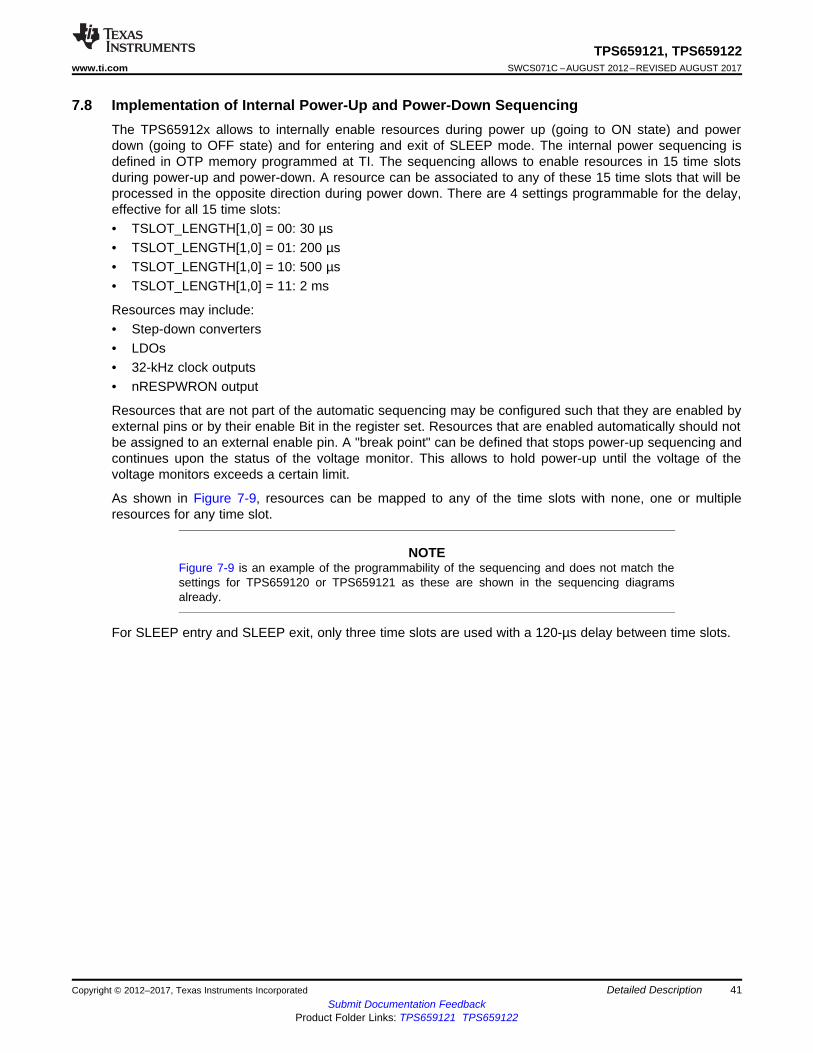
41
TPS659121, TPS659122www.ti.com SWCS071C –AUGUST 2012–REVISED AUGUST 2017
Submit Documentation FeedbackProduct Folder Links: TPS659121 TPS659122
Detailed DescriptionCopyright © 2012–2017, Texas Instruments Incorporated
7.8 Implementation of Internal Power-Up and Power-Down SequencingThe TPS65912x allows to internally enable resources during power up (going to ON state) and powerdown (going to OFF state) and for entering and exit of SLEEP mode. The internal power sequencing isdefined in OTP memory programmed at TI. The sequencing allows to enable resources in 15 time slotsduring power-up and power-down. A resource can be associated to any of these 15 time slots that will beprocessed in the opposite direction during power down. There are 4 settings programmable for the delay,effective for all 15 time slots:• TSLOT_LENGTH[1,0] = 00: 30 µs• TSLOT_LENGTH[1,0] = 01: 200 µs• TSLOT_LENGTH[1,0] = 10: 500 µs• TSLOT_LENGTH[1,0] = 11: 2 ms
Resources may include:• Step-down converters• LDOs• 32-kHz clock outputs• nRESPWRON output
Resources that are not part of the automatic sequencing may be configured such that they are enabled byexternal pins or by their enable Bit in the register set. Resources that are enabled automatically should notbe assigned to an external enable pin. A "break point" can be defined that stops power-up sequencing andcontinues upon the status of the voltage monitor. This allows to hold power-up until the voltage of thevoltage monitors exceeds a certain limit.
As shown in Figure 7-9, resources can be mapped to any of the time slots with none, one or multipleresources for any time slot.
NOTEFigure 7-9 is an example of the programmability of the sequencing and does not match thesettings for TPS659120 or TPS659121 as these are shown in the sequencing diagramsalready.
For SLEEP entry and SLEEP exit, only three time slots are used with a 120-µs delay between time slots.
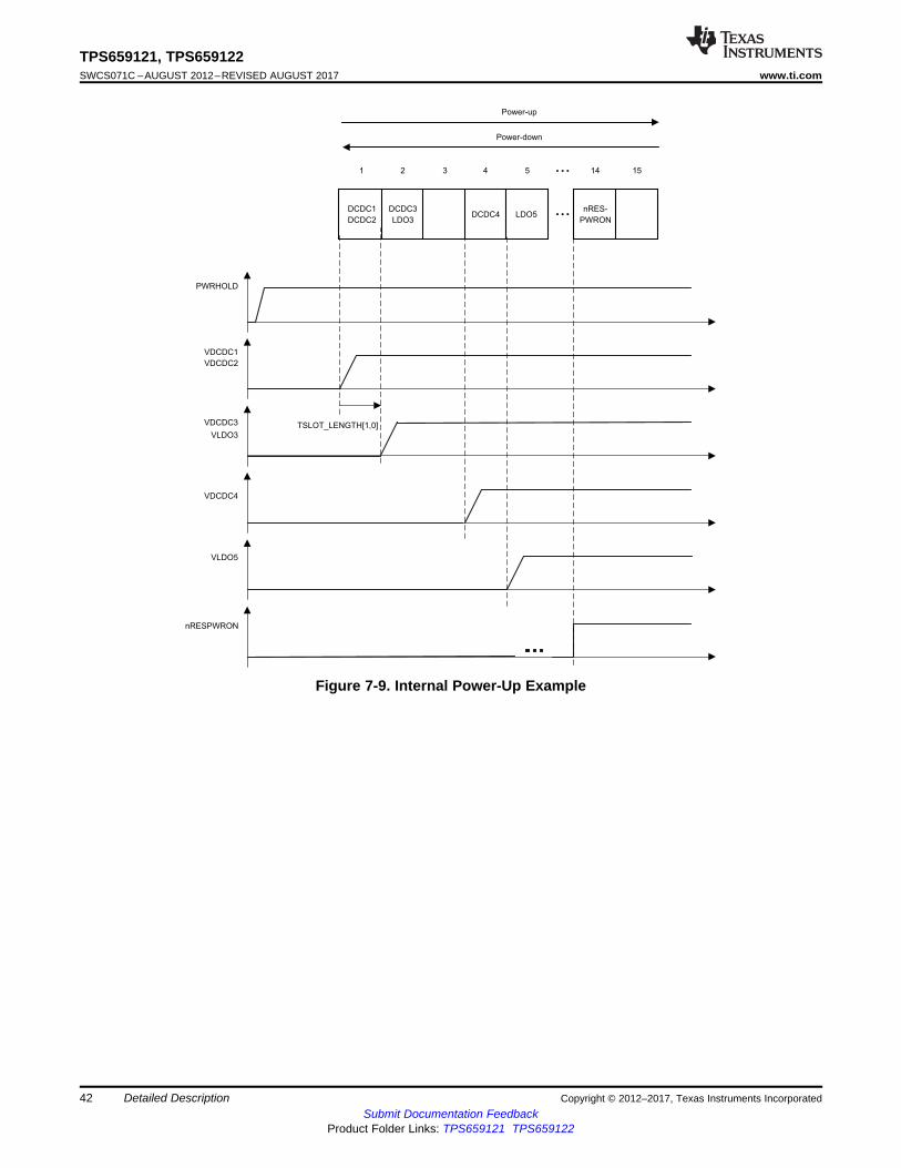
1 2 3 4 5 1514...
DCDC1
DCDC2
DCDC3
LDO3DCDC4 LDO5
nRES-
PWRON
TSLOT_LENGTH[1,0]
PWRHOLD
VDCDC1
VDCDC2
VDCDC3
VLDO3
Power-up
Power-down
VDCDC4
VLDO5
nRESPWRON
...
...
42
TPS659121, TPS659122SWCS071C –AUGUST 2012–REVISED AUGUST 2017 www.ti.com
Submit Documentation FeedbackProduct Folder Links: TPS659121 TPS659122
Detailed Description Copyright © 2012–2017, Texas Instruments Incorporated
Figure 7-9. Internal Power-Up Example
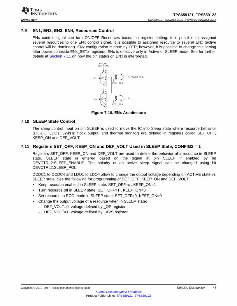
ENABLE RESx
Enx_SET(EEPROM)
EN1
ENx
RESx_REG
RESx_REG
43
TPS659121, TPS659122www.ti.com SWCS071C –AUGUST 2012–REVISED AUGUST 2017
Submit Documentation FeedbackProduct Folder Links: TPS659121 TPS659122
Detailed DescriptionCopyright © 2012–2017, Texas Instruments Incorporated
7.9 EN1, EN2, EN3, EN4, Resources ControlENx control signal can turn ON/OFF Resources based on register setting. It is possible to assignedseveral resources to one ENx control signal. It is possible to assigned resource to several ENx (activecontrol will be dominant). ENx configuration is done by OTP; however, it is possible to change this settingafter power up inside ENx_SETx registers. ENx is effective only in Active or SLEEP mode. See for furtherdetails at Section 7.11 on how the pin status on ENx is interpreted.
Figure 7-10. ENx Architecture
7.10 SLEEP State ControlThe sleep control input on pin SLEEP is used to move the IC into Sleep state where resource behavior(DC-DC, LDOs, 32-kHz clock output, and thermal monitor) are defined in registers called SET_OFF,KEEP_ON and DEF_VOLT.
7.11 Registers SET_OFF, KEEP_ON and DEF_VOLT Used in SLEEP State; CONFIG2 = 1Registers SET_OFF; KEEP_ON and DEF_VOLT are used to define the behavior of a resource in SLEEPstate. SLEEP state is entered based on the signal at pin SLEEP if enabled by bitDEVCTRL2:SLEEP_ENABLE. The polarity of an active sleep signal can be changed using bitDEVCTRL2:SLEEP_POL.
DCDC1 to DCDC4 and LDO1 to LDO4 allow to change the output voltage depending on ACTIVE state vsSLEEP state. See the following for programming of SET_OFF, KEEP_ON and DEF_VOLT:• Keep resource enabled in SLEEP state: SET_OFF=x , KEEP_ON=1• Turn resource off in SLEEP state: SET_OFF=1 , KEEP_ON=0• Set resource to ECO mode in SLEEP state: SET_OFF=0, KEEP_ON=0• Change the output voltage of a resource when in SLEEP state:
– DEF_VOLT=0: voltage defined by _OP register– DEF_VOLT=1: voltage defined by _AVS register
44
TPS659121, TPS659122SWCS071C –AUGUST 2012–REVISED AUGUST 2017 www.ti.com
Submit Documentation FeedbackProduct Folder Links: TPS659121 TPS659122
Detailed Description Copyright © 2012–2017, Texas Instruments Incorporated
7.12 Registers SET_OFF, KEEP_ON and DEF_VOLT Used for Resources Assigned to anExternal Enable Pin; CONFIG2 = 1As described in Section 7.8, a resource can be assigned to an enable pin. In this case SLEEP state hasno effect on such a resource but its behavior is defined by the state of the enable pin. RegistersSET_OFF, KEEP_ON and DEF_VOLT are re-mapped and used to define how a resource is acting whenthe enable pin is set low or is set high. The definition for an high signal on ENx is similar to an ACTIVEstate while a low signal on ENx equals the behavior in SLEEP state. See the following for a detaileddescription:• Enable resource when ENx pin is set high: SET_OFF=x , KEEP_ON=x• Disable resource when ENx pin is set low: SET_OFF=1 , KEEP_ON=0• Set resource to ECO when ENx pin is set low: SET_OFF=0, KEEP_ON=0• Change the output voltage of a resource when pin ENx is set low:
– DEF_VOLT=0: voltage defined by _OP register– DEF_VOLT=1: voltage defined by _AVS register
7.13 Registers SET_OFF, KEEP_ON and DEF_VOLT for Resources Assigned to PinsPWR_REQ, CLK_REQ1 and CLK_REQ2; CONFIG2 = 0With the CONFIG2 pin tied to GND, pins ENx are used as voltage select pins DCDCx_SEL for the DC-DCconverters and for LDOs assigned to these pins by register DEF_VOLT_MAPPING. There pins are onlyused to switch the output voltage between two values as defined in registers _OP and _AVS.• DCDCx_SEL=0: _OP registers are used to define the output voltage• DCDCx_SEL=1: _AVS registers are used to define the output voltage
The basic function of enabling or disabling resources is re-mapped to pins PWR_REQ, CLK_REQ1 andCLK_REQ2. The pin function is managed by registers ENx_SETx in the following list. Register EN4_SETxis not used and should be set 0x00.• PWR_REQ: EN1_SETx• CLK_REQ1: EN2_SETx• CLK_REQ2: EN3_SETx
7.14 Voltage Scaling Interface Control Using _OP and _AVS Registers with I2C or SPI InterfaceA dedicated I2C_AVS interface is available for voltage scaling functionality. It works in three differentmodes.• I2C voltage scaling interface where voltage target can be setup in DCDCx_OP registers.• AVSx pin called DCDCx_SEL can be used as roof or floor configuration where the DC-DC voltage
switches between the value defined in the DCDCx_OP register and the DCDCx_AVS register.
The slew rate of VDDX voltage supply reaching a new programmed value is programmable though theVDDx_REG register.
Both I2C interfaces are compliant with HS-I2C specification (100 kbits/s, 400 kbits/s, or 3.4 Mbits/s)
CONFIG1=0: OTP option A is selected
CONFIG1=1: OTP option B is selected
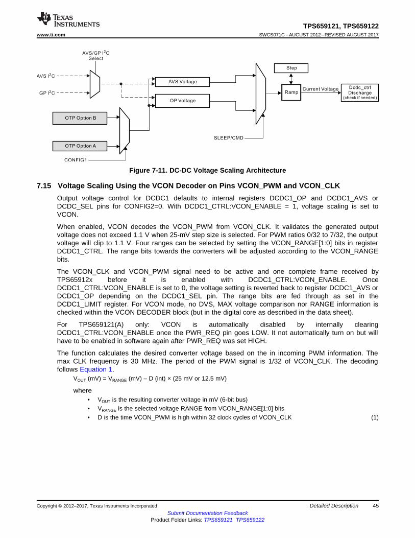
RampCurrent Voltage
Ramp
AVS Voltage
OTP Option B
OP Voltage
OTP Option A
Step
Dcdc_ctrlDischarge
(check if needed)
SLEEP/CMD
CONFIG1
AVS/GP I CSelect
2
AVS I C2
GP I C2
45
TPS659121, TPS659122www.ti.com SWCS071C –AUGUST 2012–REVISED AUGUST 2017
Submit Documentation FeedbackProduct Folder Links: TPS659121 TPS659122
Detailed DescriptionCopyright © 2012–2017, Texas Instruments Incorporated
Figure 7-11. DC-DC Voltage Scaling Architecture
7.15 Voltage Scaling Using the VCON Decoder on Pins VCON_PWM and VCON_CLKOutput voltage control for DCDC1 defaults to internal registers DCDC1_OP and DCDC1_AVS orDCDC_SEL pins for CONFIG2=0. With DCDC1_CTRL:VCON_ENABLE = 1, voltage scaling is set toVCON.
When enabled, VCON decodes the VCON_PWM from VCON_CLK. It validates the generated outputvoltage does not exceed 1.1 V when 25-mV step size is selected. For PWM ratios 0/32 to 7/32, the outputvoltage will clip to 1.1 V. Four ranges can be selected by setting the VCON_RANGE[1:0] bits in registerDCDC1_CTRL. The range bits towards the converters will be adjusted according to the VCON_RANGEbits.
The VCON_CLK and VCON_PWM signal need to be active and one complete frame received byTPS65912x before it is enabled with DCDC1_CTRL:VCON_ENABLE. OnceDCDC1_CTRL:VCON_ENABLE is set to 0, the voltage setting is reverted back to register DCDC1_AVS orDCDC1_OP depending on the DCDC1_SEL pin. The range bits are fed through as set in theDCDC1_LIMIT register. For VCON mode, no DVS, MAX voltage comparison nor RANGE information ischecked within the VCON DECODER block (but in the digital core as described in the data sheet).
For TPS659121(A) only: VCON is automatically disabled by internally clearingDCDC1_CTRL:VCON_ENABLE once the PWR_REQ pin goes LOW. It not automatically turn on but willhave to be enabled in software again after PWR_REQ was set HIGH.
The function calculates the desired converter voltage based on the in incoming PWM information. Themax CLK frequency is 30 MHz. The period of the PWM signal is 1/32 of VCON_CLK. The decodingfollows Equation 1.
VOUT (mV) = VRANGE (mV) – D (int) × (25 mV or 12.5 mV)
where• VOUT is the resulting converter voltage in mV (6-bit bus)• VRANGE is the selected voltage RANGE from VCON_RANGE[1:0] bits• D is the time VCON_PWM is high within 32 clock cycles of VCON_CLK (1)
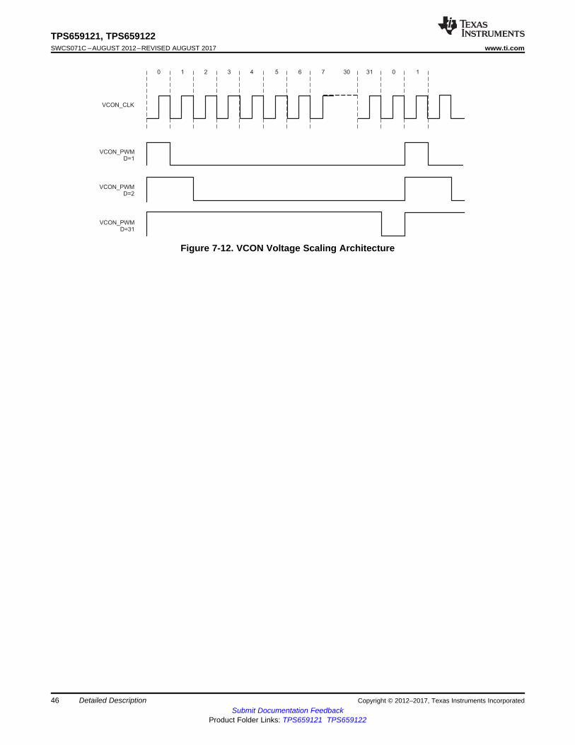
VCON_CLK
VCON_PWMD=1
VCON_PWMD=2
VCON_PWMD=31
0 1 2 3 4 5 6 7 30 31 0 1
46
TPS659121, TPS659122SWCS071C –AUGUST 2012–REVISED AUGUST 2017 www.ti.com
Submit Documentation FeedbackProduct Folder Links: TPS659121 TPS659122
Detailed Description Copyright © 2012–2017, Texas Instruments Incorporated
Figure 7-12. VCON Voltage Scaling Architecture
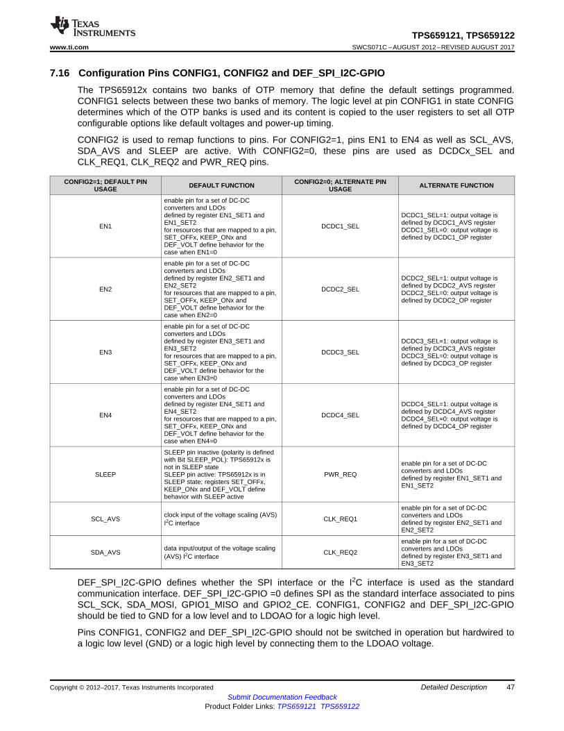
47
TPS659121, TPS659122www.ti.com SWCS071C –AUGUST 2012–REVISED AUGUST 2017
Submit Documentation FeedbackProduct Folder Links: TPS659121 TPS659122
Detailed DescriptionCopyright © 2012–2017, Texas Instruments Incorporated
7.16 Configuration Pins CONFIG1, CONFIG2 and DEF_SPI_I2C-GPIOThe TPS65912x contains two banks of OTP memory that define the default settings programmed.CONFIG1 selects between these two banks of memory. The logic level at pin CONFIG1 in state CONFIGdetermines which of the OTP banks is used and its content is copied to the user registers to set all OTPconfigurable options like default voltages and power-up timing.
CONFIG2 is used to remap functions to pins. For CONFIG2=1, pins EN1 to EN4 as well as SCL_AVS,SDA_AVS and SLEEP are active. With CONFIG2=0, these pins are used as DCDCx_SEL andCLK_REQ1, CLK_REQ2 and PWR_REQ pins.
CONFIG2=1; DEFAULT PINUSAGE DEFAULT FUNCTION CONFIG2=0; ALTERNATE PIN
USAGE ALTERNATE FUNCTION
EN1
enable pin for a set of DC-DCconverters and LDOsdefined by register EN1_SET1 andEN1_SET2for resources that are mapped to a pin,SET_OFFx, KEEP_ONx andDEF_VOLT define behavior for thecase when EN1=0
DCDC1_SEL
DCDC1_SEL=1: output voltage isdefined by DCDC1_AVS registerDCDC1_SEL=0: output voltage isdefined by DCDC1_OP register
EN2
enable pin for a set of DC-DCconverters and LDOsdefined by register EN2_SET1 andEN2_SET2for resources that are mapped to a pin,SET_OFFx, KEEP_ONx andDEF_VOLT define behavior for thecase when EN2=0
DCDC2_SEL
DCDC2_SEL=1: output voltage isdefined by DCDC2_AVS registerDCDC2_SEL=0: output voltage isdefined by DCDC2_OP register
EN3
enable pin for a set of DC-DCconverters and LDOsdefined by register EN3_SET1 andEN3_SET2for resources that are mapped to a pin,SET_OFFx, KEEP_ONx andDEF_VOLT define behavior for thecase when EN3=0
DCDC3_SEL
DCDC3_SEL=1: output voltage isdefined by DCDC3_AVS registerDCDC3_SEL=0: output voltage isdefined by DCDC3_OP register
EN4
enable pin for a set of DC-DCconverters and LDOsdefined by register EN4_SET1 andEN4_SET2for resources that are mapped to a pin,SET_OFFx, KEEP_ONx andDEF_VOLT define behavior for thecase when EN4=0
DCDC4_SEL
DCDC4_SEL=1: output voltage isdefined by DCDC4_AVS registerDCDC4_SEL=0: output voltage isdefined by DCDC4_OP register
SLEEP
SLEEP pin inactive (polarity is definedwith Bit SLEEP_POL): TPS65912x isnot in SLEEP stateSLEEP pin active: TPS65912x is inSLEEP state; registers SET_OFFx,KEEP_ONx and DEF_VOLT definebehavior with SLEEP active
PWR_REQ
enable pin for a set of DC-DCconverters and LDOsdefined by register EN1_SET1 andEN1_SET2
SCL_AVS clock input of the voltage scaling (AVS)I2C interface CLK_REQ1
enable pin for a set of DC-DCconverters and LDOsdefined by register EN2_SET1 andEN2_SET2
SDA_AVS data input/output of the voltage scaling(AVS) I2C interface CLK_REQ2
enable pin for a set of DC-DCconverters and LDOsdefined by register EN3_SET1 andEN3_SET2
DEF_SPI_I2C-GPIO defines whether the SPI interface or the I2C interface is used as the standardcommunication interface. DEF_SPI_I2C-GPIO =0 defines SPI as the standard interface associated to pinsSCL_SCK, SDA_MOSI, GPIO1_MISO and GPIO2_CE. CONFIG1, CONFIG2 and DEF_SPI_I2C-GPIOshould be tied to GND for a low level and to LDOAO for a logic high level.
Pins CONFIG1, CONFIG2 and DEF_SPI_I2C-GPIO should not be switched in operation but hardwired toa logic low level (GND) or a logic high level by connecting them to the LDOAO voltage.
48
TPS659121, TPS659122SWCS071C –AUGUST 2012–REVISED AUGUST 2017 www.ti.com
Submit Documentation FeedbackProduct Folder Links: TPS659121 TPS659122
Detailed Description Copyright © 2012–2017, Texas Instruments Incorporated
7.17 VDDIO Voltage for Push-Pull Output StagesThere is a number of outputs that can either be configured as a push-pull output or are push-pull outputsonly. Any pin with a push-pull output stage will generate its output high level by the voltage applied to pinVDDIO. The input voltage range on VDDIO is 1.6 V to 3.3 V with an undervoltage lockout below 1.6 V.With a VDDIO voltage below the undervoltage lockout threshold, the high side driver of the push-pulloutput stages are disabled and the output default back to open drain. Pins affected are listed below:• nRESPWRON push-pull or open drain defined by DEVCTRL:Bit3• INT1 push-pull or open drain defined by DEVCTRL2:Bit6• VSUP_OUT same pin with nRESPWRON, definition by DEVCTRL:Bit3• GPIO1, GPIO2: push-pull only• GPIO3, GPIO4, GPIO5: push-pull or open drain managed by GPIOx registers• 32-kHz CLKOUT: alternative function to OMAP_WDI (input); switched to output by CONFIG2=0,
switched to input with CONFIG2=1; push-pull only if output with CONFIG2=0: CPCAP_WDI is set to 0with CONFIG2=1: CPCAP_WDI is the output of the AND gate
7.18 Digital Signal Summary• SLEEP:
– When all SLEEP condition are met (no pending interrupt, Sleep Ball low, Sleep register set to 1),The IC is transitioning to SLEEP which impact LDO/DC-DC behavior based on settings defined inregisters SET_OFF, KEEP_ON and DEF_VOLT. An interrupt or a SLEEP pin level change willcause a transition back to ACTIVE state. This input signal is level sensitive and no debouncing isapplied. SLEEP is configurable and is disabled by default, so at power up its status will be ignored.In a user register it can be enabled and its active level changed between active HIGH or activeLOW using bits SLEEP_POL and SLEEP_ENABLE in register DEVCTRL2.
• PWRHOLD:– PWRHOLD pin can be used as ON/OFF signal input (when nPWRON and Interrupt not used). It
can also be used as acknowledge (Maintain Power) of power-up sequence trigger by interrupt orpress of nPWRON. This input signal is level sensitive and no debouncing is applied. Rising and/orfalling edge of PWRHOLD is highlighted through an associated interrupt if interrupt is unmasked.
• NRESPWRON/VSUP_OUT:– NRESPWRON signal is used as the reset to the processor and is in VDDIO domain. It is held low
until the ACTIVE state is reached. See Section 7.19, Section 7.20 to get detailed timing.– VSUP_OUT is the output of the voltage monitor that can alternatively be used as a reset to a
processor or included in the power-up sequencing such that it hold power up until its output is HIGHor the device power down when LOW.
• 32KCLKOUT:– This signal is the output of the 32K RC oscillator, which can be enabled or not during the power-on
sequence. It can be enabled and disabled by register bit, during ACTIVE state of the device.• nPWRON:
– The nPWRON input is connected to an external button. A debounced falling edge on this signalcauses a OFF to ACTIVE state transition of the device. If the device is in ACTIVE/SLEEP modethen a low level on this signal generates an interrupt. If the nPWRON signal is low for more thanthe PWON_TO_OFF_DELAY delay and the corresponding interrupt is not acknowledged by theexternal processor in TBDs then the device will go to OFF state.
49
TPS659121, TPS659122www.ti.com SWCS071C –AUGUST 2012–REVISED AUGUST 2017
Submit Documentation FeedbackProduct Folder Links: TPS659121 TPS659122
Detailed DescriptionCopyright © 2012–2017, Texas Instruments Incorporated
• INT1:– INT1 signal (active low) warns the host processor of any event that occurred on the TPS65912x
device. The host processor can then poll the interrupt from the interrupt status register via I2C toidentify the interrupt source. A low level indicates an active interrupt, highlighted in the INT_STSxregisters. Interrupt flag active will generate a POWER ON enable condition pulse of lengthTDOINT1 only when the device is in OFF state (when NRESPWRON signal is low). The POWERON enable condition pulse will occur only if the interrupt status bit is initially low (no previousinterrupt pending in the status register). Interrupt status register must be cleared first to allowdevice POWER OFF during the TDOINT1 pulse duration. Any of the interrupt sources can bemasked programming INT_MSKx registers. The default setting is masking all interrupts. When aninterrupt is masked, its corresponding interrupt status bit is still updated, but the INT1 flag is notactivated. Interrupt source masking can be used to mask a device switch-on event. The INT outputcan be programmed as push-pull or open drain output stage with either active LOW or active HIGHoutput defined by two OTP settings.
• GPIO1, GPIO2, GPIO3, GPIO4, GPIO5:– GPIO functionality are muxed with LED and SPI interface. It can be used for event detection or
control of external resources during power up.• VCCS_VIN_MON:
– This is the input for the internal undervoltage lockout monitor. The block provides a selectable lowbattery warning as well as a undervoltage shutdown.
• VCON_CLK; VCON_PWM:– Clock and data input for voltage scaling of DCDC1. The feature is enabled by TBD Bit. When
enabled, voltage scaling through DCDC1_OP and DCDC1_AVS registers is blocked.• CLK, MOSI, MISO,CE:
– Clock chip enable and master in slave out (MISO) and master out slave in MOSI pins for the SPIinterface. The pins are shared with the standard I2C interface SCL and SDA and GPIO1 and GPIO2
• DEF_SPI_I2C-GPIO:– Defines whether multifunction pins are used for the SPI interface or for the I2C interface and
GPIOs. For DEF_SPI_I2C-GPIO = 0, the function is assigned to the SPI interface on pins CLK,MOSI, MISO, CE. For DEF_SPI_I2C-GPIO = 1, the function is assigned to the I2C interface andGPIOs on pins SCL, SDA, GPIO1 and GPIO2.
• SCL_AVS, SDA_AVS:– Power I2C interface, typically used for DVS on the step-down converters. There is a Bit on each
step-down converter to switch the voltage scaling registers from the standard I2C interface or SPIinterface to the power-I2C interface. When switched to power-I2C, the register is blocked for accessthrough the standard interface.
7.19 TPS659121 On/Off Operation With E450, E500
7.19.1 TPS659121 Power Up From Battery or 5-V USB Supply; CONFIG1=LOWPWRHOLD is tied to the supply voltage so TPS65912x starts its power-up sequencing once the inputvoltage is above the UVLO threshold. After DCDC2, DCDC3 and LDO10 are powered, further power up ispending the status of the voltage monitor based on the VIN_MON voltage. Once the voltage is above thethreshold, VSUP_OUT goes high and power-up sequencing continues. DCDC1 and LDO1 are controlledby the status of their enable pin PWR_REQ. CLK_REQ1 and CLK_REQ2 are logically OR´d to enableLDO4 and LDO5.
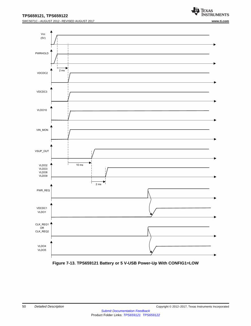
VIN_MON
VLDO2
VLDO3
VLDO8
VLDO9
VDCDC2
PWRHOLD
2 ms
Vcc
(5V)
VSUP_OUT
VLDO10
VDCDC3
VDCDC1
VLDO1
10 ms
2 ms
PWR_REQ
VLDO4
VLDO5
CLK_REQ1
OR
CLK_REQ2
50
TPS659121, TPS659122SWCS071C –AUGUST 2012–REVISED AUGUST 2017 www.ti.com
Submit Documentation FeedbackProduct Folder Links: TPS659121 TPS659122
Detailed Description Copyright © 2012–2017, Texas Instruments Incorporated
Figure 7-13. TPS659121 Battery or 5 V-USB Power-Up With CONFIG1=LOW
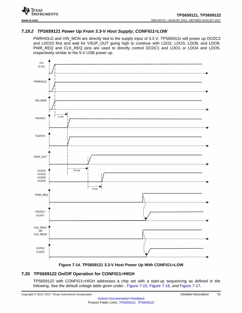
VLDO2
VLDO3
VLDO8
VLDO9
VIN_MON
PWRHOLD
2 ms
Vcc
(3.3V)
VSUP_OUT
VLDO10
VDCDC2
VDCDC1
VLDO1
10 ms
PWR_REQ
VLDO4
VLDO5
CLK_REQ1
OR
CLK_REQ2
2 ms
51
TPS659121, TPS659122www.ti.com SWCS071C –AUGUST 2012–REVISED AUGUST 2017
Submit Documentation FeedbackProduct Folder Links: TPS659121 TPS659122
Detailed DescriptionCopyright © 2012–2017, Texas Instruments Incorporated
7.19.2 TPS659121 Power Up From 3.3-V Host Supply; CONFIG1=LOWPWRHOLD and VIN_MON are directly tied to the supply input of 3.3 V. TPS65912x will power up DCDC2and LDO10 first and wait for VSUP_OUT going high to continue with LDO2, LDO3, LDO8, and LDO9.PWR_REQ and CLK_REQ pins are used to directly control DCDC1 and LDO1 or LDO4 and LDO5,respectively similar to the 5-V USB power up.
Figure 7-14. TPS659121 3.3-V Host Power Up With CONFIG1=LOW
7.20 TPS659122 On/Off Operation for CONFIG1=HIGHTPS659122 with CONFIG1=HIGH addresses a chip set with a start-up sequencing as defined in thefollowing. See the default voltage table given under , Figure 7-15, Figure 7-16, and Figure 7-17.
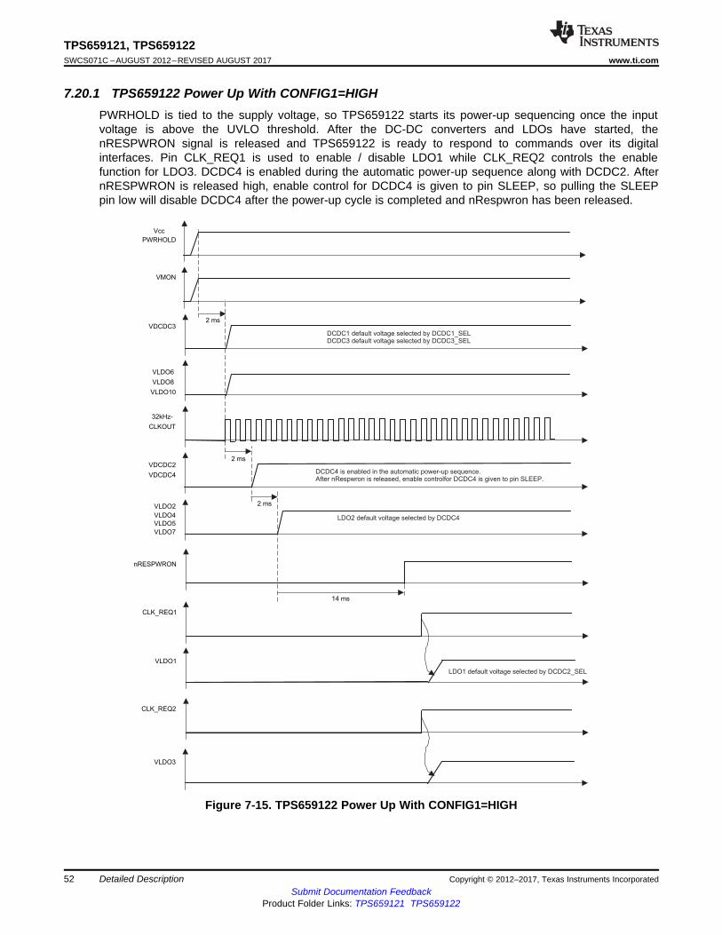
VDCDC2
VDCDC4
VLDO2
VLDO4
VLDO5
VLDO7
VDCDC3
Vcc
PWRHOLD
2 ms
32kHz-
CLKOUT
VLDO6
VLDO8
VLDO10
nRESPWRON
VLDO1
CLK_REQ1
2 ms
2 ms
14 ms
VMON
DCDC1 default voltage selected by DCDC1_SELDCDC3 default voltage selected by DCDC3_SEL
DCDC4 is enabled in the automatic power-up sequence.After nRespwron is released, enable controlfor DCDC4 is given to pin SLEEP.
LDO2 default voltage selected by DCDC4
LDO1 default voltage selected by DCDC2_SEL
CLK_REQ2
VLDO3
52
TPS659121, TPS659122SWCS071C –AUGUST 2012–REVISED AUGUST 2017 www.ti.com
Submit Documentation FeedbackProduct Folder Links: TPS659121 TPS659122
Detailed Description Copyright © 2012–2017, Texas Instruments Incorporated
7.20.1 TPS659122 Power Up With CONFIG1=HIGHPWRHOLD is tied to the supply voltage, so TPS659122 starts its power-up sequencing once the inputvoltage is above the UVLO threshold. After the DC-DC converters and LDOs have started, thenRESPWRON signal is released and TPS659122 is ready to respond to commands over its digitalinterfaces. Pin CLK_REQ1 is used to enable / disable LDO1 while CLK_REQ2 controls the enablefunction for LDO3. DCDC4 is enabled during the automatic power-up sequence along with DCDC2. AfternRESPWRON is released high, enable control for DCDC4 is given to pin SLEEP, so pulling the SLEEPpin low will disable DCDC4 after the power-up cycle is completed and nRespwron has been released.
Figure 7-15. TPS659122 Power Up With CONFIG1=HIGH
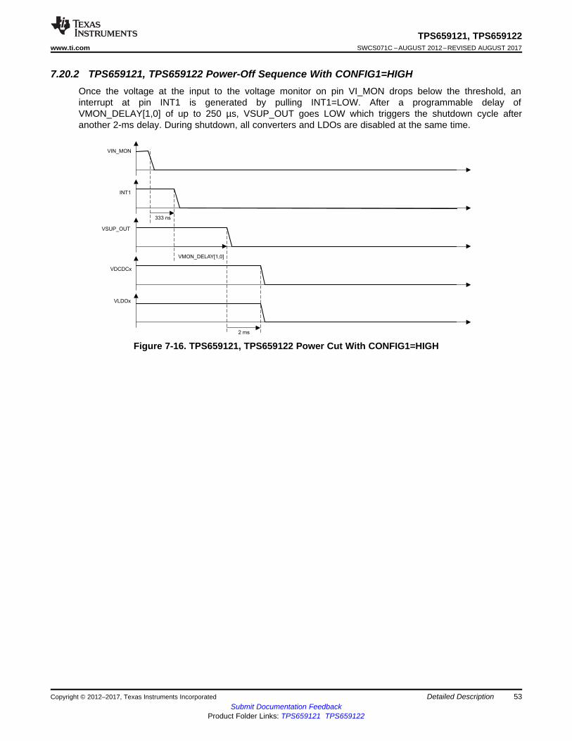
VLDOx
VIN_MON
333 ns
VSUP_OUT
INT1
VMON_DELAY[1,0]
2 ms
VDCDCx
53
TPS659121, TPS659122www.ti.com SWCS071C –AUGUST 2012–REVISED AUGUST 2017
Submit Documentation FeedbackProduct Folder Links: TPS659121 TPS659122
Detailed DescriptionCopyright © 2012–2017, Texas Instruments Incorporated
7.20.2 TPS659121, TPS659122 Power-Off Sequence With CONFIG1=HIGHOnce the voltage at the input to the voltage monitor on pin VI_MON drops below the threshold, aninterrupt at pin INT1 is generated by pulling INT1=LOW. After a programmable delay ofVMON_DELAY[1,0] of up to 250 µs, VSUP_OUT goes LOW which triggers the shutdown cycle afteranother 2-ms delay. During shutdown, all converters and LDOs are disabled at the same time.
Figure 7-16. TPS659121, TPS659122 Power Cut With CONFIG1=HIGH
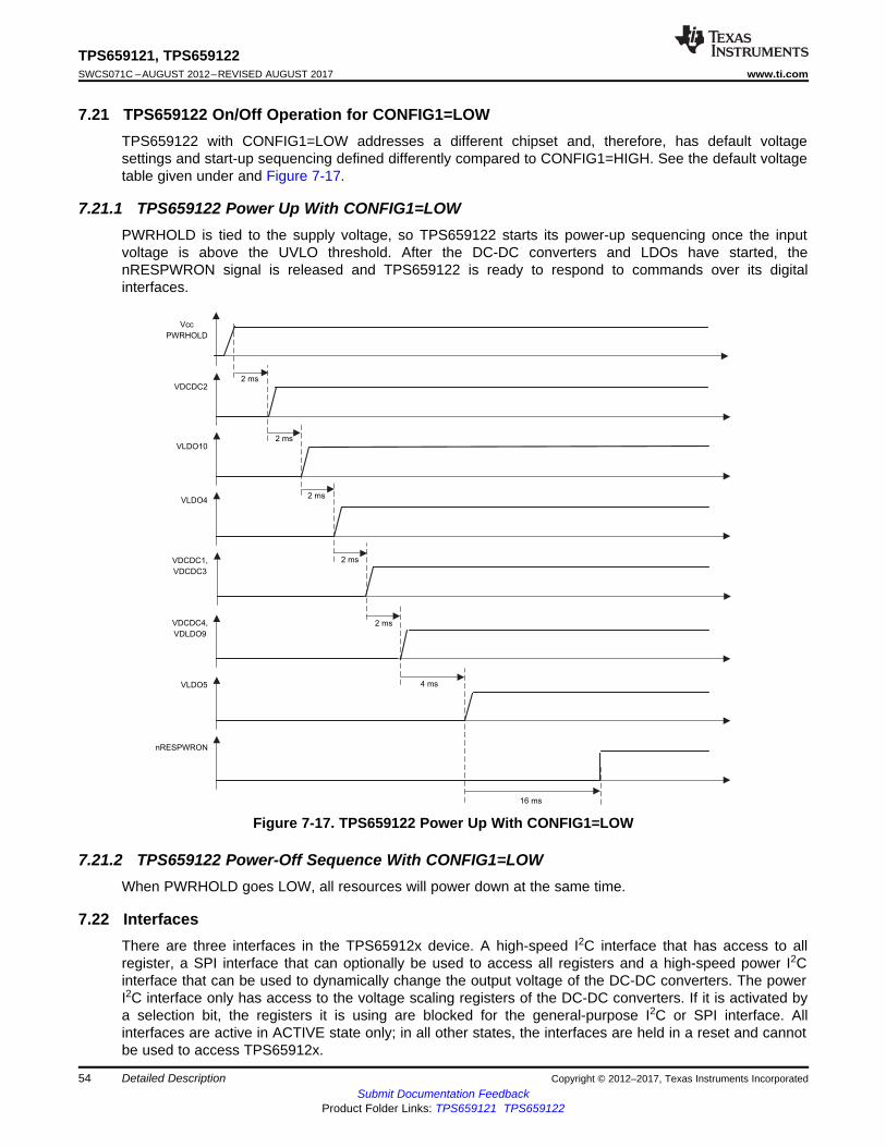
VLDO10
VLDO4
VDCDC2
Vcc
PWRHOLD
2 ms
2 ms
nRESPWRON
2 ms
2 ms
16 ms
VDCDC1,
VDCDC3
VDCDC4,
VDLDO9
2 ms
VLDO5 4 ms
54
TPS659121, TPS659122SWCS071C –AUGUST 2012–REVISED AUGUST 2017 www.ti.com
Submit Documentation FeedbackProduct Folder Links: TPS659121 TPS659122
Detailed Description Copyright © 2012–2017, Texas Instruments Incorporated
7.21 TPS659122 On/Off Operation for CONFIG1=LOWTPS659122 with CONFIG1=LOW addresses a different chipset and, therefore, has default voltagesettings and start-up sequencing defined differently compared to CONFIG1=HIGH. See the default voltagetable given under and Figure 7-17.
7.21.1 TPS659122 Power Up With CONFIG1=LOWPWRHOLD is tied to the supply voltage, so TPS659122 starts its power-up sequencing once the inputvoltage is above the UVLO threshold. After the DC-DC converters and LDOs have started, thenRESPWRON signal is released and TPS659122 is ready to respond to commands over its digitalinterfaces.
Figure 7-17. TPS659122 Power Up With CONFIG1=LOW
7.21.2 TPS659122 Power-Off Sequence With CONFIG1=LOWWhen PWRHOLD goes LOW, all resources will power down at the same time.
7.22 InterfacesThere are three interfaces in the TPS65912x device. A high-speed I2C interface that has access to allregister, a SPI interface that can optionally be used to access all registers and a high-speed power I2Cinterface that can be used to dynamically change the output voltage of the DC-DC converters. The powerI2C interface only has access to the voltage scaling registers of the DC-DC converters. If it is activated bya selection bit, the registers it is using are blocked for the general-purpose I2C or SPI interface. Allinterfaces are active in ACTIVE state only; in all other states, the interfaces are held in a reset and cannotbe used to access TPS65912x.
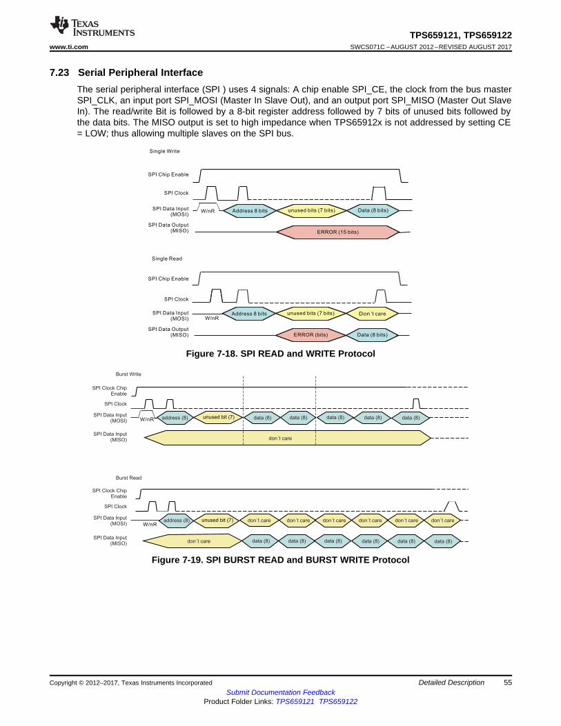
unused bit (7)
unused bit (7) data (8) data (8) data (8) data (8) data (8)W/nR
don´t careW/nR
address (8)
address (8)
data (8)data (8)data (8)data (8)data (8)data (8)
don´t care don´t care don´t care don´t care don´t care
don´t care
don´t care
Burst Write
Burst Read
SPI Clock ChipEnable
SPI Clock
SPI Data Input(MOSI)
SPI Data Input(MISO)
SPI Clock ChipEnable
SPI Clock
SPI Data Input(MOSI)
SPI Data Input(MISO)
W/nR Address 8 bits unused bits (7 bits) Data (8 bits)
ERROR (15 bits)
Single Write
Address 8 bits unused bits (7 bits) Don ’t care
Data (8 bits)ERROR (bits)
Single Read
SPI Chip Enable
SPI Clock
SPI Data Input(MOSI)
SPI Data Output(MISO)
SPI Chip Enable
SPI Clock
SPI Data Input(MOSI)
SPI Data Output(MISO)
W/nR
55
TPS659121, TPS659122www.ti.com SWCS071C –AUGUST 2012–REVISED AUGUST 2017
Submit Documentation FeedbackProduct Folder Links: TPS659121 TPS659122
Detailed DescriptionCopyright © 2012–2017, Texas Instruments Incorporated
7.23 Serial Peripheral InterfaceThe serial peripheral interface (SPI ) uses 4 signals: A chip enable SPI_CE, the clock from the bus masterSPI_CLK, an input port SPI_MOSI (Master In Slave Out), and an output port SPI_MISO (Master Out SlaveIn). The read/write Bit is followed by a 8-bit register address followed by 7 bits of unused bits followed bythe data bits. The MISO output is set to high impedance when TPS65912x is not addressed by setting CE= LOW; thus allowing multiple slaves on the SPI bus.
Figure 7-18. SPI READ and WRITE Protocol
Figure 7-19. SPI BURST READ and BURST WRITE Protocol
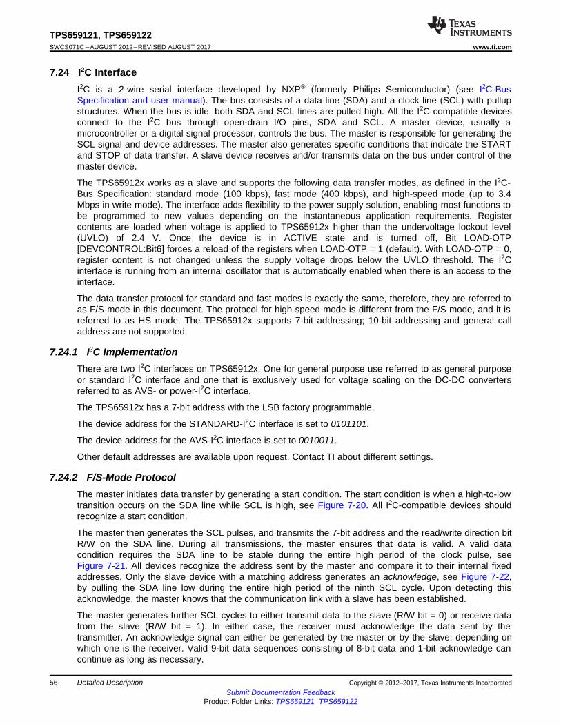
56
TPS659121, TPS659122SWCS071C –AUGUST 2012–REVISED AUGUST 2017 www.ti.com
Submit Documentation FeedbackProduct Folder Links: TPS659121 TPS659122
Detailed Description Copyright © 2012–2017, Texas Instruments Incorporated
7.24 I2C InterfaceI2C is a 2-wire serial interface developed by NXP® (formerly Philips Semiconductor) (see I2C-BusSpecification and user manual). The bus consists of a data line (SDA) and a clock line (SCL) with pullupstructures. When the bus is idle, both SDA and SCL lines are pulled high. All the I2C compatible devicesconnect to the I2C bus through open-drain I/O pins, SDA and SCL. A master device, usually amicrocontroller or a digital signal processor, controls the bus. The master is responsible for generating theSCL signal and device addresses. The master also generates specific conditions that indicate the STARTand STOP of data transfer. A slave device receives and/or transmits data on the bus under control of themaster device.
The TPS65912x works as a slave and supports the following data transfer modes, as defined in the I2C-Bus Specification: standard mode (100 kbps), fast mode (400 kbps), and high-speed mode (up to 3.4Mbps in write mode). The interface adds flexibility to the power supply solution, enabling most functions tobe programmed to new values depending on the instantaneous application requirements. Registercontents are loaded when voltage is applied to TPS65912x higher than the undervoltage lockout level(UVLO) of 2.4 V. Once the device is in ACTIVE state and is turned off, Bit LOAD-OTP[DEVCONTROL:Bit6] forces a reload of the registers when LOAD-OTP = 1 (default). With LOAD-OTP = 0,register content is not changed unless the supply voltage drops below the UVLO threshold. The I2Cinterface is running from an internal oscillator that is automatically enabled when there is an access to theinterface.
The data transfer protocol for standard and fast modes is exactly the same, therefore, they are referred toas F/S-mode in this document. The protocol for high-speed mode is different from the F/S mode, and it isreferred to as HS mode. The TPS65912x supports 7-bit addressing; 10-bit addressing and general calladdress are not supported.
7.24.1 I2C ImplementationThere are two I2C interfaces on TPS65912x. One for general purpose use referred to as general purposeor standard I2C interface and one that is exclusively used for voltage scaling on the DC-DC convertersreferred to as AVS- or power-I2C interface.
The TPS65912x has a 7-bit address with the LSB factory programmable.
The device address for the STANDARD-I2C interface is set to 0101101.
The device address for the AVS-I2C interface is set to 0010011.
Other default addresses are available upon request. Contact TI about different settings.
7.24.2 F/S-Mode ProtocolThe master initiates data transfer by generating a start condition. The start condition is when a high-to-lowtransition occurs on the SDA line while SCL is high, see Figure 7-20. All I2C-compatible devices shouldrecognize a start condition.
The master then generates the SCL pulses, and transmits the 7-bit address and the read/write direction bitR/W on the SDA line. During all transmissions, the master ensures that data is valid. A valid datacondition requires the SDA line to be stable during the entire high period of the clock pulse, seeFigure 7-21. All devices recognize the address sent by the master and compare it to their internal fixedaddresses. Only the slave device with a matching address generates an acknowledge, see Figure 7-22,by pulling the SDA line low during the entire high period of the ninth SCL cycle. Upon detecting thisacknowledge, the master knows that the communication link with a slave has been established.
The master generates further SCL cycles to either transmit data to the slave (R/W bit = 0) or receive datafrom the slave (R/W bit = 1). In either case, the receiver must acknowledge the data sent by thetransmitter. An acknowledge signal can either be generated by the master or by the slave, depending onwhich one is the receiver. Valid 9-bit data sequences consisting of 8-bit data and 1-bit acknowledge cancontinue as long as necessary.
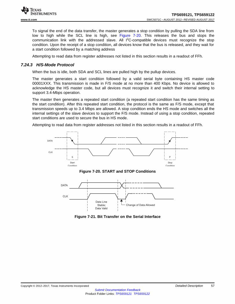
Change of Data Allowed
Data Line
Stable;
Data Valid
DATA
CLK
Start
Condition
DATA
Stop
Condition
CLK
S P
57
TPS659121, TPS659122www.ti.com SWCS071C –AUGUST 2012–REVISED AUGUST 2017
Submit Documentation FeedbackProduct Folder Links: TPS659121 TPS659122
Detailed DescriptionCopyright © 2012–2017, Texas Instruments Incorporated
To signal the end of the data transfer, the master generates a stop condition by pulling the SDA line fromlow to high while the SCL line is high, see Figure 7-20. This releases the bus and stops thecommunication link with the addressed slave. All I2C-compatible devices must recognize the stopcondition. Upon the receipt of a stop condition, all devices know that the bus is released, and they wait fora start condition followed by a matching address
Attempting to read data from register addresses not listed in this section results in a readout of FFh.
7.24.3 H/S-Mode ProtocolWhen the bus is idle, both SDA and SCL lines are pulled high by the pullup devices.
The master generates a start condition followed by a valid serial byte containing HS master code00001XXX. This transmission is made in F/S mode at no more than 400 Kbps. No device is allowed toacknowledge the HS master code, but all devices must recognize it and switch their internal setting tosupport 3.4-Mbps operation.
The master then generates a repeated start condition (a repeated start condition has the same timing asthe start condition). After this repeated start condition, the protocol is the same as F/S mode, except thattransmission speeds up to 3.4 Mbps are allowed. A stop condition ends the HS mode and switches all theinternal settings of the slave devices to support the F/S mode. Instead of using a stop condition, repeatedstart conditions are used to secure the bus in HS mode.
Attempting to read data from register addresses not listed in this section results in a readout of FFh.
Figure 7-20. START and STOP Conditions
Figure 7-21. Bit Transfer on the Serial Interface
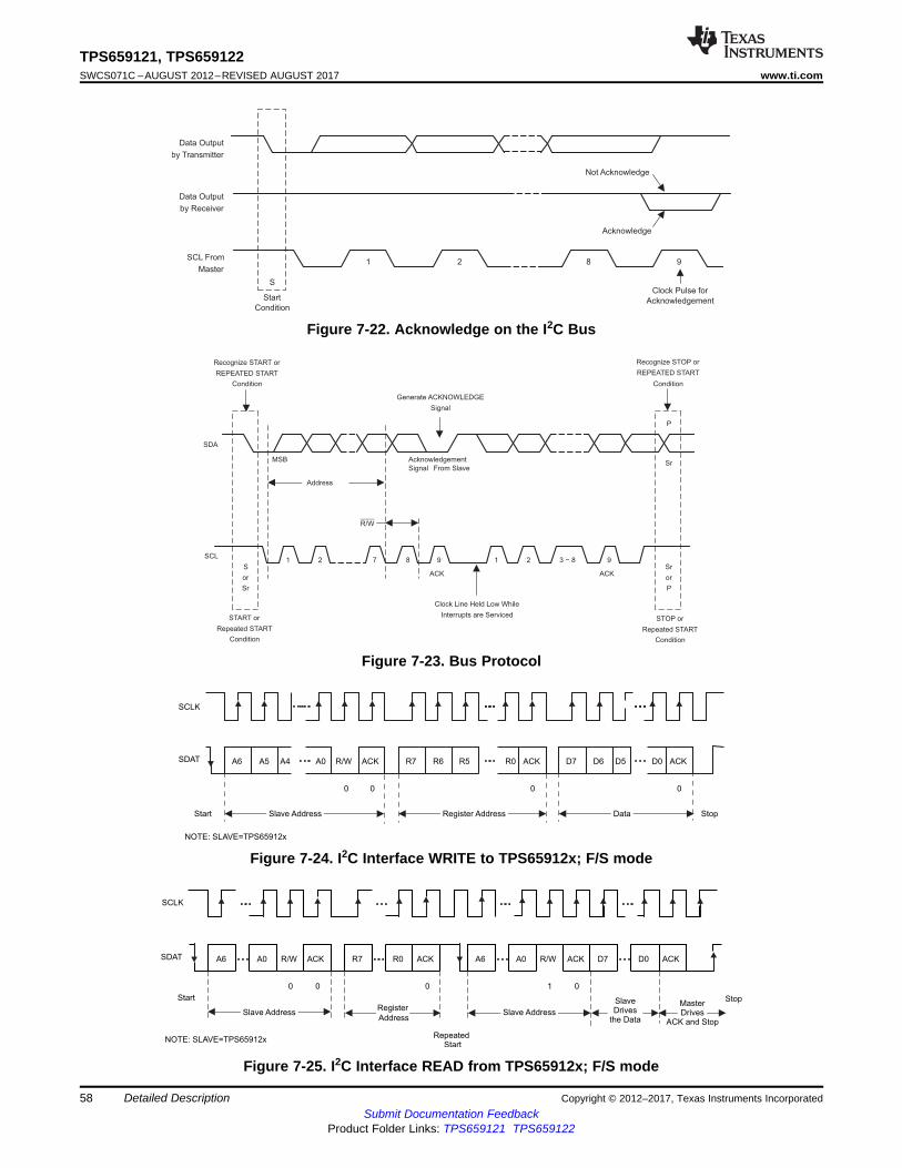
SCLK
SDAT A6 R0 ACKR7ACKR/WA0
0 0 0 0
StopStart
NOTE: SLAVE=TPS65912x
ACKD0D7ACKR/WA0A6
1
RepeatedStart
Slave AddressRegister
AddressSlave Address
SlaveDrives
the Data
MasterDrives
ACK and Stop
SCLK
SDAT A6 R6 R5 R0 ACK D7 D6 D5 D0 ACKR7ACKR/WA0A4A5
0 0 0 0
StopStart
NOTE: SLAVE=TPS65912x
DataSlave Address Register Address
Recognize START or
REPEATED START
Condition
Recognize STOP or
REPEATED START
Condition
Generate ACKNOWLEDGE
Signal
Acknowledgement
Signal From Slave
SDA
SCL
MSB
P
Sr
Sr
or
P
S
or
Sr
START or
Repeated START
Condition
STOP or
Repeated START
Condition
Clock Line Held Low While
Interrupts are Serviced
1 2 7 8 9
ACK
1 2 3 − 8 9
ACK
Address
R/W
Not Acknowledge
Acknowledge
1 2 8 9
Clock Pulse for
Acknowledgement
S
Start
Condition
Data Output
by Transmitter
Data Output
by Receiver
SCL From
Master
58
TPS659121, TPS659122SWCS071C –AUGUST 2012–REVISED AUGUST 2017 www.ti.com
Submit Documentation FeedbackProduct Folder Links: TPS659121 TPS659122
Detailed Description Copyright © 2012–2017, Texas Instruments Incorporated
Figure 7-22. Acknowledge on the I2C Bus
Figure 7-23. Bus Protocol
Figure 7-24. I2C Interface WRITE to TPS65912x; F/S mode
Figure 7-25. I2C Interface READ from TPS65912x; F/S mode
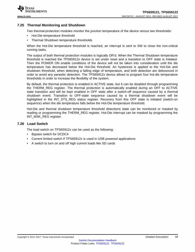
59
TPS659121, TPS659122www.ti.com SWCS071C –AUGUST 2012–REVISED AUGUST 2017
Submit Documentation FeedbackProduct Folder Links: TPS659121 TPS659122
Detailed DescriptionCopyright © 2012–2017, Texas Instruments Incorporated
7.25 Thermal Monitoring and ShutdownTwo thermal-protection modules monitor the junction temperature of the device versus two thresholds:• Hot-Die temperature threshold• Thermal Shutdown temperature thresholds
When the Hot-Die temperature threshold is reached, an interrupt is sent to SW to close the non-criticalrunning tasks.
The output of both thermal protection modules is logically OR’d. When the Thermal Shutdown temperaturethreshold is reached the TPS65912x device is set under reset and a transition to OFF state is initiated.Then the POWER ON enable conditions of the device will not be taken into consideration until the dietemperature has decreased below the Hot-Die threshold. An hysteresis is applied to the Hot-Die andshutdown threshold, when detecting a falling edge of temperature, and both detection are debounced inorder to avoid any parasitic detection. The TPS65912x device allows to program four hot-die temperaturethresholds in order to increase the flexibility of the system.
By default, the thermal protection is enabled in ACTIVE state, but It can be disabled through programmingthe THERM_REG register. The thermal protection is automatically enabled during an OFF to ACTIVEstate transition and will be kept enabled in OFF state after a switch-off sequence caused by a thermalshutdown event. Transition to OFF-state sequence caused by a thermal shutdown event will behighlighted in the INT_STS_REG status register. Recovery from this OFF state is initiated (switch-onsequence) when the die temperature falls below the Hot-Die temperature threshold.
Hot-Die and thermal shutdown temperature threshold detections state can be monitored or masked byreading or programming the THERM_REG register. Hot-Die interrupt can be masked by programming theINT_MSK_REG register.
7.26 Load SwitchThe load switch on TPS65912x can be used as the following:• Bypass switch for DCDC4• Current limited switch if TPS65912x is used in USB powered applications• A switch to turn on and off high current loads like SD cards
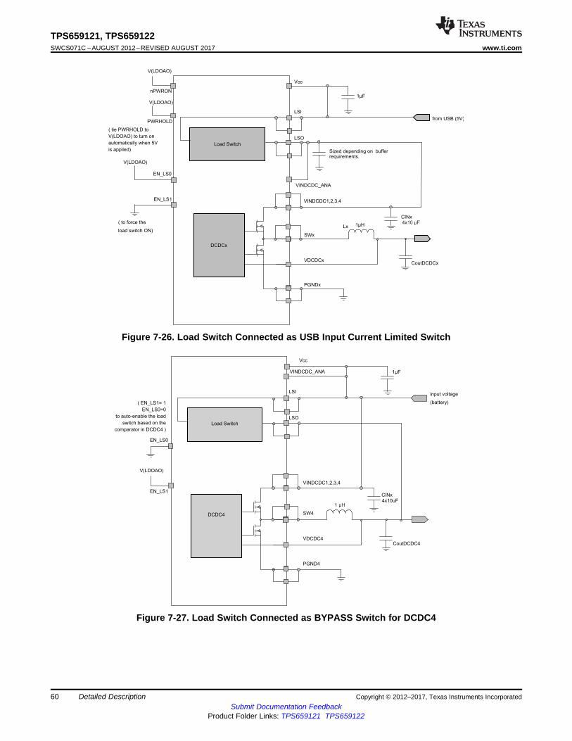
DCDC4
VDCDC4
VINDCDC1,2,3,4
4x10uF
PGND4
CoutDCDC4
CINx
Load Switch
input voltage
(battery)
LSI
LSO
Vcc
1µFVINDCDC_ANA
EN_LS0
EN_LS1
V(LDOAO)
( EN_LS1= 1
EN_LS0=0
to auto-enable the load
switch based on the
comparator in DCDC4 )
1 µH
SW4
SWx
DCDCx
VDCDCx
VINDCDC1,2,3,4
PGNDx
Lx
CoutDCDCx
CINx
Load Switch
from USB (5V)
LSI
LSO
Vcc
1µF
Sized depending on bufferrequirements.
VINDCDC_ANA
EN_LS0
EN_LS1
V(LDOAO)
( to force the
load switch ON)
V(LDOAO)
nPWRON
V(LDOAO)
PWRHOLD
( tie PWRHOLD to
V(LDOAO) to turn on
automatically when 5V
is applied)
4x10 µF1µH
60
TPS659121, TPS659122SWCS071C –AUGUST 2012–REVISED AUGUST 2017 www.ti.com
Submit Documentation FeedbackProduct Folder Links: TPS659121 TPS659122
Detailed Description Copyright © 2012–2017, Texas Instruments Incorporated
Figure 7-26. Load Switch Connected as USB Input Current Limited Switch
Figure 7-27. Load Switch Connected as BYPASS Switch for DCDC4
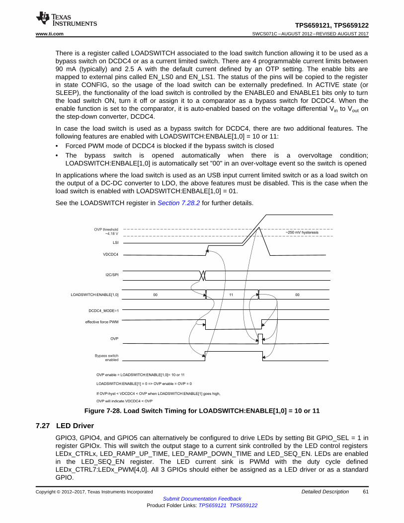
VDCDC4
I2C/SPI
LOADSWITCH:ENABLE[1,0]
DCDC4_MODE=1
effective force PWM
OVP
LSI
00 11 00
OVP enable = LOADSWITCH:ENABLE[1,0]= 10 or 11
LOADSWITCH:ENABLE[1] = 0 => OVP enable = OVP = 0
~250 mV hysteresis
If OVP-hyst < VDCDC4 < OVP when LOADSWITCH:ENABLE[1] goes high,
OVP will indicate VDCDC4 < OVP
OVP threshold~4.18 V
Bypass switchenabled
61
TPS659121, TPS659122www.ti.com SWCS071C –AUGUST 2012–REVISED AUGUST 2017
Submit Documentation FeedbackProduct Folder Links: TPS659121 TPS659122
Detailed DescriptionCopyright © 2012–2017, Texas Instruments Incorporated
There is a register called LOADSWITCH associated to the load switch function allowing it to be used as abypass switch on DCDC4 or as a current limited switch. There are 4 programmable current limits between90 mA (typically) and 2.5 A with the default current defined by an OTP setting. The enable bits aremapped to external pins called EN_LS0 and EN_LS1. The status of the pins will be copied to the registerin state CONFIG, so the usage of the load switch can be externally predefined. In ACTIVE state (orSLEEP), the functionality of the load switch is controlled by the ENABLE0 and ENABLE1 bits only to turnthe load switch ON, turn it off or assign it to a comparator as a bypass switch for DCDC4. When theenable function is set to the comparator, it is auto-enabled based on the voltage differential Vin to Vout onthe step-down converter, DCDC4.
In case the load switch is used as a bypass switch for DCDC4, there are two additional features. Thefollowing features are enabled with LOADSWITCH:ENBALE[1,0] = 10 or 11:• Forced PWM mode of DCDC4 is blocked if the bypass switch is closed• The bypass switch is opened automatically when there is a overvoltage condition;
LOADSWITCH:ENBALE[1,0] is automatically set "00" in an over-voltage event so the switch is opened
In applications where the load switch is used as an USB input current limited switch or as a load switch onthe output of a DC-DC converter to LDO, the above features must be disabled. This is the case when theload switch is enabled with LOADSWITCH:ENBALE[1,0] = 01.
See the LOADSWITCH register in Section 7.28.2 for further details.
Figure 7-28. Load Switch Timing for LOADSWITCH:ENABLE[1,0] = 10 or 11
7.27 LED DriverGPIO3, GPIO4, and GPIO5 can alternatively be configured to drive LEDs by setting Bit GPIO_SEL = 1 inregister GPIOx. This will switch the output stage to a current sink controlled by the LED control registersLEDx_CTRLx, LED_RAMP_UP_TIME, LED_RAMP_DOWN_TIME and LED_SEQ_EN. LEDs are enabledin the LED_SEQ_EN register. The LED current sink is PWMd with the duty cycle definedLEDx_CTRL7:LEDx_PWM[4,0]. All 3 GPIOs should either be assigned as a LED driver or as a standardGPIO.
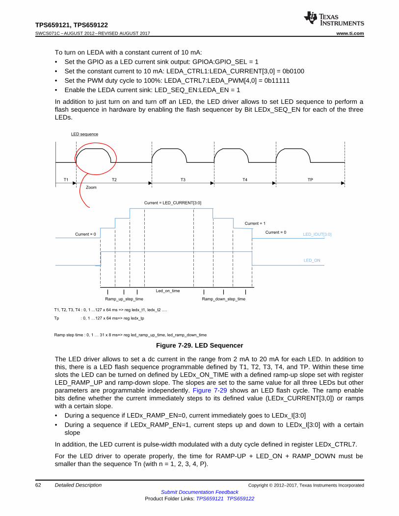
LED sequence
Ramp_up_step_time Ramp_down_step_time
Led_on_time
Current = 0
Zoom
T1, T2, T3, T4 : 0, 1 ...127 x 64 ms => reg ledx_t1, ledx_t2 ….
Tp : 0, 1 …127 x 64 ms=> reg ledx_tp
Ramp step time : 0, 1 … 31 x 8 ms=> reg led_ramp_up_time, led_ramp_down_time
T1 T2 T3 T4 TP
Current = 1
Current = LED_CURRENT[3:0]
Current = 0LED_IOUT[3:0]
LED_ON
62
TPS659121, TPS659122SWCS071C –AUGUST 2012–REVISED AUGUST 2017 www.ti.com
Submit Documentation FeedbackProduct Folder Links: TPS659121 TPS659122
Detailed Description Copyright © 2012–2017, Texas Instruments Incorporated
To turn on LEDA with a constant current of 10 mA:• Set the GPIO as a LED current sink output: GPIOA:GPIO_SEL = 1• Set the constant current to 10 mA: LEDA_CTRL1:LEDA_CURRENT[3,0] = 0b0100• Set the PWM duty cycle to 100%: LEDA_CTRL7:LEDA_PWM[4,0] = 0b11111• Enable the LEDA current sink: LED_SEQ_EN:LEDA_EN = 1
In addition to just turn on and turn off an LED, the LED driver allows to set LED sequence to perform aflash sequence in hardware by enabling the flash sequencer by Bit LEDx_SEQ_EN for each of the threeLEDs.
Figure 7-29. LED Sequencer
The LED driver allows to set a dc current in the range from 2 mA to 20 mA for each LED. In addition tothis, there is a LED flash sequence programmable defined by T1, T2, T3, T4, and TP. Within these timeslots the LED can be turned on defined by LEDx_ON_TIME with a defined ramp-up slope set with registerLED_RAMP_UP and ramp-down slope. The slopes are set to the same value for all three LEDs but otherparameters are programmable independently. Figure 7-29 shows an LED flash cycle. The ramp enablebits define whether the current immediately steps to its defined value (LEDx_CURRENT[3,0]) or rampswith a certain slope.• During a sequence if LEDx_RAMP_EN=0, current immediately goes to LEDx_I[3:0]• During a sequence if LEDx_RAMP_EN=1, current steps up and down to LEDx_I[3:0] with a certain
slope
In addition, the LED current is pulse-width modulated with a duty cycle defined in register LEDx_CTRL7.
For the LED driver to operate properly, the time for RAMP-UP + LED_ON + RAMP_DOWN must besmaller than the sequence Tn (with n = 1, 2, 3, 4, P).
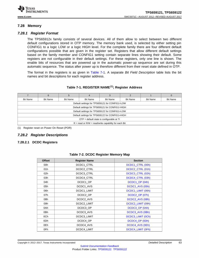
63
TPS659121, TPS659122www.ti.com SWCS071C –AUGUST 2012–REVISED AUGUST 2017
Submit Documentation FeedbackProduct Folder Links: TPS659121 TPS659122
Detailed DescriptionCopyright © 2012–2017, Texas Instruments Incorporated
7.28 Memory
7.28.1 Register FormatThe TPS65912x family consists of several devices. All of them allow to select between two differentdefault configurations stored in OTP memory. The memory bank used, is selected by either setting pinCONFIG1 to a logic LOW or a logic HIGH level. For the complete family there are four different defaultconfigurations possible that are given in the register set. Registers that allow different default settingsbased on the family member and CONFIG1 setting contain separate lines showing their default. Someregisters are not configurable in their default settings. For these registers, only one line is shown. Theenable bits of resources that are powered up in the automatic power-up sequence are set during thisautomatic sequence. The status after power up is therefore different from their reset state defined in OTP.
The format in the registers is as given in Table 7-1. A separate Bit Field Description table lists the bitnames and bit descriptions for each register address.
(1) Register reset on Power On Reset (POR)
Table 7-1. REGISTER NAME (1); Register Address
7 6 5 4 3 2 1 0
Bit Name Bit Name Bit Name Bit Name Bit Name Bit Name Bit Name Bit Name
Default settings for TPS659121 for CONFIG1=LOW
Default settings for TPS659121 for CONFIG1=HIGH
Default settings for TPS659122 for CONFIG1=LOW
Default settings for TPS659122 for CONFIG1=HIGH
OTP = default state is configurable at TI
R = read or R/W = read/write capability for each Bit
7.28.2 Register Descriptions
7.28.2.1 DCDC Registers
Table 7-2. DCDC Register Memory Map
Offset Register Name Section00h DCDC1_CTRL DCDC1_CTRL (00h)01h DCDC2_CTRL DCDC2_CTRL (01h)02h DCDC3_CTRL DCDC3_CTRL (02h)03h DCDC4_CTRL DCDC4_CTRL (03h)04h DCDC1_OP DCDC1_OP (04h)05h DCDC1_AVS DCDC1_AVS (05h)06h DCDC1_LIMIT DCDC1_LIMIT (06h)07h DCDC2_OP DCDC2_OP (07h)08h DCDC2_AVS DCDC2_AVS (08h)09h DCDC2_LIMIT DCDC2_LIMIT (09h)0Ah DCDC3_OP DCDC3_OP (0Ah)0Bh DCDC3_AVS DCDC3_AVS (0Bh)0Ch DCDC3_LIMIT DCDC3_LIMIT (0Ch)0Dh DCDC4_OP DCDC4_OP (0Dh)0Eh DCDC4_AVS DCDC4_AVS (0Eh)0Fh DCDC4_LIMIT DCDC4_LIMIT (0Fh)
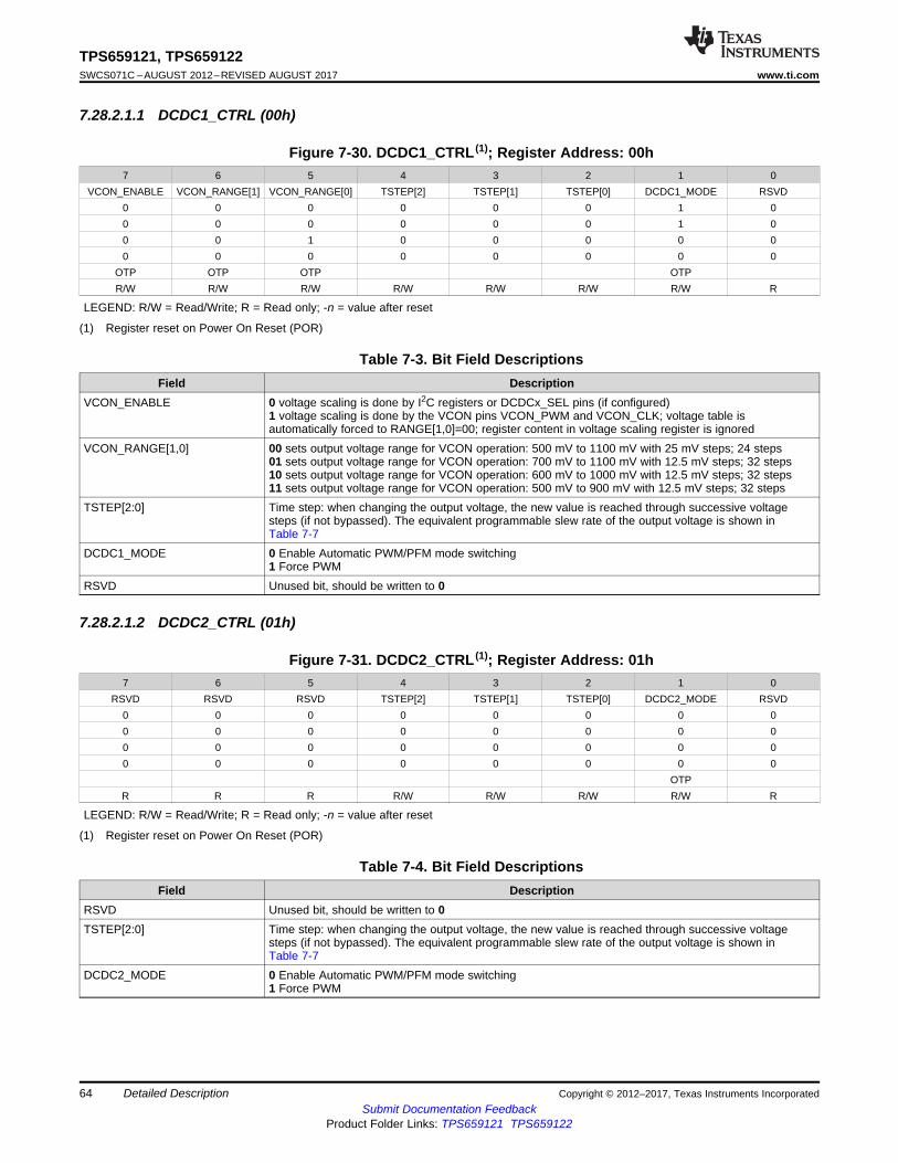
64
TPS659121, TPS659122SWCS071C –AUGUST 2012–REVISED AUGUST 2017 www.ti.com
Submit Documentation FeedbackProduct Folder Links: TPS659121 TPS659122
Detailed Description Copyright © 2012–2017, Texas Instruments Incorporated
7.28.2.1.1 DCDC1_CTRL (00h)
(1) Register reset on Power On Reset (POR)
Figure 7-30. DCDC1_CTRL (1); Register Address: 00h7 6 5 4 3 2 1 0
VCON_ENABLE VCON_RANGE[1] VCON_RANGE[0] TSTEP[2] TSTEP[1] TSTEP[0] DCDC1_MODE RSVD0 0 0 0 0 0 1 00 0 0 0 0 0 1 00 0 1 0 0 0 0 00 0 0 0 0 0 0 0
OTP OTP OTP OTPR/W R/W R/W R/W R/W R/W R/W R
LEGEND: R/W = Read/Write; R = Read only; -n = value after reset
Table 7-3. Bit Field DescriptionsField Description
VCON_ENABLE 0 voltage scaling is done by I2C registers or DCDCx_SEL pins (if configured)1 voltage scaling is done by the VCON pins VCON_PWM and VCON_CLK; voltage table isautomatically forced to RANGE[1,0]=00; register content in voltage scaling register is ignored
VCON_RANGE[1,0] 00 sets output voltage range for VCON operation: 500 mV to 1100 mV with 25 mV steps; 24 steps01 sets output voltage range for VCON operation: 700 mV to 1100 mV with 12.5 mV steps; 32 steps10 sets output voltage range for VCON operation: 600 mV to 1000 mV with 12.5 mV steps; 32 steps11 sets output voltage range for VCON operation: 500 mV to 900 mV with 12.5 mV steps; 32 steps
TSTEP[2:0] Time step: when changing the output voltage, the new value is reached through successive voltagesteps (if not bypassed). The equivalent programmable slew rate of the output voltage is shown inTable 7-7
DCDC1_MODE 0 Enable Automatic PWM/PFM mode switching1 Force PWM
RSVD Unused bit, should be written to 0
7.28.2.1.2 DCDC2_CTRL (01h)
(1) Register reset on Power On Reset (POR)
Figure 7-31. DCDC2_CTRL (1); Register Address: 01h7 6 5 4 3 2 1 0
RSVD RSVD RSVD TSTEP[2] TSTEP[1] TSTEP[0] DCDC2_MODE RSVD0 0 0 0 0 0 0 00 0 0 0 0 0 0 00 0 0 0 0 0 0 00 0 0 0 0 0 0 0
OTPR R R R/W R/W R/W R/W R
LEGEND: R/W = Read/Write; R = Read only; -n = value after reset
Table 7-4. Bit Field DescriptionsField Description
RSVD Unused bit, should be written to 0TSTEP[2:0] Time step: when changing the output voltage, the new value is reached through successive voltage
steps (if not bypassed). The equivalent programmable slew rate of the output voltage is shown inTable 7-7
DCDC2_MODE 0 Enable Automatic PWM/PFM mode switching1 Force PWM
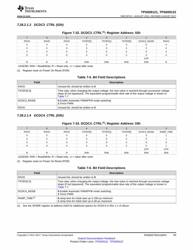
65
TPS659121, TPS659122www.ti.com SWCS071C –AUGUST 2012–REVISED AUGUST 2017
Submit Documentation FeedbackProduct Folder Links: TPS659121 TPS659122
Detailed DescriptionCopyright © 2012–2017, Texas Instruments Incorporated
7.28.2.1.3 DCDC3_CTRL (02h)
(1) Register reset on Power On Reset (POR)
Figure 7-32. DCDC3_CTRL (1); Register Address: 02h7 6 5 4 3 2 1 0
RSVD RSVD RSVD TSTEP[2] TSTEP[1] TSTEP[0] DCDC3_MODE RSVD0 0 0 0 0 0 0 00 0 0 0 0 0 0 00 0 0 0 0 0 0 00 0 0 0 0 0 0 0
OTPR R R R/W R/W R/W R/W R
LEGEND: R/W = Read/Write; R = Read only; -n = value after reset
Table 7-5. Bit Field DescriptionsField Description
RSVD Unused bit, should be written to 0TSTEP[2:0] Time step: when changing the output voltage, the new value is reached through successive voltage
steps (if not bypassed). The equivalent programmable slew rate of the output voltage is shown inTable 7-7
DCDC3_MODE 0 Enable Automatic PWM/PFM mode switching1 Force PWM
RSVD Unused bit, should be written to 0
7.28.2.1.4 DCDC4_CTRL (03h)
(1) Register reset on Power On Reset (POR)
Figure 7-33. DCDC4_CTRL (1); Register Address: 03h7 6 5 4 3 2 1 0
RSVD RSVD RSVD TSTEP[2] TSTEP[1] TSTEP[0] DCDC4_MODE RAMP_TIME0 0 0 0 0 0 0 10 0 0 0 0 0 0 10 0 0 0 0 0 0 00 0 0 0 0 0 0 1
OTP OTPR R R R/W R/W R/W R/W R/W
LEGEND: R/W = Read/Write; R = Read only; -n = value after reset
(1) See the SPARE register at address 0x63 for additional options for DCDC4 in Rev 1.1 of silicon
Table 7-6. Bit Field DescriptionsField Description
RSVD Unused bit, should be written to 0TSTEP[2:0] Time step: when changing the output voltage, the new value is reached through successive voltage
steps (if not bypassed). The equivalent programmable slew rate of the output voltage is shown inTable 7-7
DCDC4_MODE 0 Enable Automatic PWM/PFM mode switching1 Force PWM
RAMP_TIME (1) 0 ramp time for initial start up is 200-µs minimum1 ramp time for initial start up is 60-µs maximum
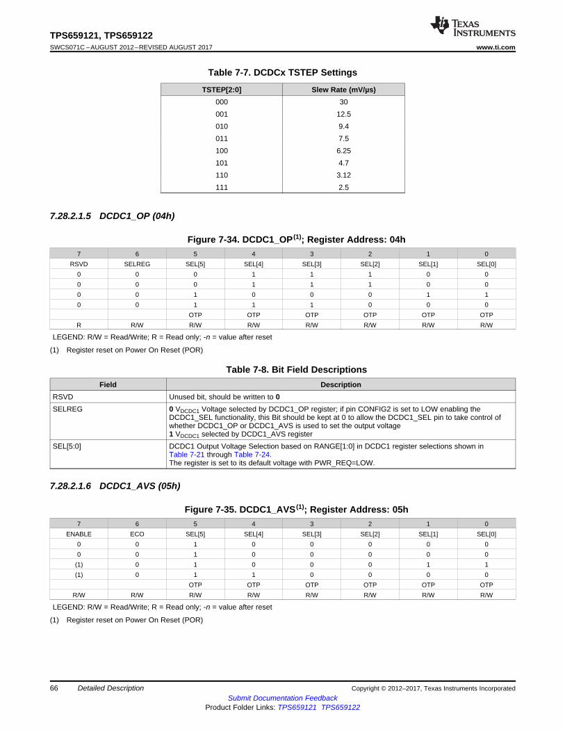
66
TPS659121, TPS659122SWCS071C –AUGUST 2012–REVISED AUGUST 2017 www.ti.com
Submit Documentation FeedbackProduct Folder Links: TPS659121 TPS659122
Detailed Description Copyright © 2012–2017, Texas Instruments Incorporated
Table 7-7. DCDCx TSTEP Settings
TSTEP[2:0] Slew Rate (mV/µs)000 30001 12.5010 9.4011 7.5100 6.25101 4.7110 3.12111 2.5
7.28.2.1.5 DCDC1_OP (04h)
(1) Register reset on Power On Reset (POR)
Figure 7-34. DCDC1_OP (1); Register Address: 04h7 6 5 4 3 2 1 0
RSVD SELREG SEL[5] SEL[4] SEL[3] SEL[2] SEL[1] SEL[0]0 0 0 1 1 1 0 00 0 0 1 1 1 0 00 0 1 0 0 0 1 10 0 1 1 1 0 0 0
OTP OTP OTP OTP OTP OTPR R/W R/W R/W R/W R/W R/W R/W
LEGEND: R/W = Read/Write; R = Read only; -n = value after reset
Table 7-8. Bit Field DescriptionsField Description
RSVD Unused bit, should be written to 0SELREG 0 VDCDC1 Voltage selected by DCDC1_OP register; if pin CONFIG2 is set to LOW enabling the
DCDC1_SEL functionality, this Bit should be kept at 0 to allow the DCDC1_SEL pin to take control ofwhether DCDC1_OP or DCDC1_AVS is used to set the output voltage1 VDCDC1 selected by DCDC1_AVS register
SEL[5:0] DCDC1 Output Voltage Selection based on RANGE[1:0] in DCDC1 register selections shown inTable 7-21 through Table 7-24.The register is set to its default voltage with PWR_REQ=LOW.
7.28.2.1.6 DCDC1_AVS (05h)
(1) Register reset on Power On Reset (POR)
Figure 7-35. DCDC1_AVS (1); Register Address: 05h7 6 5 4 3 2 1 0
ENABLE ECO SEL[5] SEL[4] SEL[3] SEL[2] SEL[1] SEL[0]0 0 1 0 0 0 0 00 0 1 0 0 0 0 0
(1) 0 1 0 0 0 1 1(1) 0 1 1 0 0 0 0
OTP OTP OTP OTP OTP OTPR/W R/W R/W R/W R/W R/W R/W R/W
LEGEND: R/W = Read/Write; R = Read only; -n = value after reset
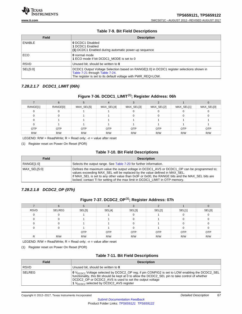
67
TPS659121, TPS659122www.ti.com SWCS071C –AUGUST 2012–REVISED AUGUST 2017
Submit Documentation FeedbackProduct Folder Links: TPS659121 TPS659122
Detailed DescriptionCopyright © 2012–2017, Texas Instruments Incorporated
Table 7-9. Bit Field DescriptionsField Description
ENABLE 0 DCDC1 Disabled1 DCDC1 Enabled(1) DCDC1 Enabled during automatic power-up sequence
ECO 0 normal mode1 ECO mode if bit DCDC1_MODE is set to 0
RSVD Unused bit, should be written to 0SEL[5:0] DCDC1 Output Voltage Selection based on RANGE[1:0] in DCDC1 register selections shown in
Table 7-21 through Table 7-24.The register is set to its default voltage with PWR_REQ=LOW.
7.28.2.1.7 DCDC1_LIMIT (06h)
(1) Register reset on Power On Reset (POR)
Figure 7-36. DCDC1_LIMIT (1); Register Address: 06h7 6 5 4 3 2 1 0
RANGE[1] RANGE[0] MAX_SEL[5] MAX_SEL[4] MAX_SEL[3] MAX_SEL[2] MAX_SEL[1] MAX_SEL[0]0 0 1 1 0 0 0 00 0 1 1 0 0 0 00 1 1 1 1 1 1 10 1 1 1 1 1 1 1
OTP OTP OTP OTP OTP OTP OTP OTPR/W R/W R/W R/W R/W R/W R/W R/W
LEGEND: R/W = Read/Write; R = Read only; -n = value after reset
Table 7-10. Bit Field DescriptionsField Description
RANGE[1:0] Selects the output range. See Table 7-20 for further information.MAX_SEL[5:0] Defines the maximum value the output voltage in DCDC1_AVS or DCDC1_OP can be programmed to;
values exceeding MAX_SEL will be replaced by the value defined in MAX_SEL.If MAX_SEL is set to any other value than 0x3F or 0x00, the RANGE bits and the MAX_SEL bits arelocked; contact TI for setting of the max limit in DCDC1_LIMIT in OTP memory.
7.28.2.1.8 DCDC2_OP (07h)
(1) Register reset on Power On Reset (POR)
Figure 7-37. DCDC2_OP (1); Register Address: 07h7 6 5 4 3 2 1 0
RSVD SELREG SEL[5] SEL[4] SEL[3] SEL[2] SEL[1] SEL[0]0 0 1 1 0 1 0 00 0 1 1 0 1 0 00 0 1 1 0 1 0 00 0 1 1 0 1 0 0
OTP OTP OTP OTP OTP OTPR R/W R/W R/W R/W R/W R/W R/W
LEGEND: R/W = Read/Write; R = Read only; -n = value after reset
Table 7-11. Bit Field DescriptionsField Description
RSVD Unused bit, should be written to 0SELREG 0 VDCDC2 Voltage selected by DCDC2_OP reg; if pin CONFIG2 is set to LOW enabling the DCDC2_SEL
functionality, this Bit should be kept at 0 to allow the DCDC2_SEL pin to take control of whetherDCDC2_OP or DCDC2_AVS is used to set the output voltage1 VDCDC2 selected by DCDC2_AVS register
68
TPS659121, TPS659122SWCS071C –AUGUST 2012–REVISED AUGUST 2017 www.ti.com
Submit Documentation FeedbackProduct Folder Links: TPS659121 TPS659122
Detailed Description Copyright © 2012–2017, Texas Instruments Incorporated
Table 7-11. Bit Field Descriptions (continued)Field Description
SEL[5:0] DCDC2 Output Voltage Selection based on RANGE[1:0] in DCDC2 register selections shown inTable 7-21 through Table 7-24.
7.28.2.1.9 DCDC2_AVS (08h)
(1) Register reset on Power On Reset (POR)
Figure 7-38. DCDC2_AVS (1); Register Address: 08h7 6 5 4 3 2 1 0
ENABLE ECO SEL[5] SEL[4] SEL[3] SEL[2] SEL[1] SEL[0](1) 0 1 1 1 1 0 0(1) 0 1 1 1 1 0 0(1) 0 1 1 0 1 0 0(1) 0 1 1 0 1 0 0
OTP OTP OTP OTP OTP OTPR/W R/W R/W R/W R/W R/W R/W R/W
LEGEND: R/W = Read/Write; R = Read only; -n = value after reset
Table 7-12. Bit Field DescriptionsField Description
ENABLE 0 DCDC2 Disabled1 DCDC2 Enabled(1) DCDC2 Enabled during automatic power-up sequence
ECO 0 normal mode1 ECO mode if bit DCDC2_MODE is set to 0
RSVD Unused bit, should be written to 0SEL[5:0] DCDC2 Output Voltage Selection based on RANGE[1:0] in DCDC2 register selections shown in
Table 7-21 through Table 7-24.
7.28.2.1.10 DCDC2_LIMIT (09h)
(1) Register reset on Power On Reset (POR)
Figure 7-39. DCDC2_LIMIT (1); Register Address: 09h7 6 5 4 3 2 1 0
RANGE[1] RANGE[0] MAX_SEL[5] MAX_SEL[4] MAX_SEL[3] MAX_SEL[2] MAX_SEL[1] MAX_SEL[0]1 0 1 1 1 1 1 11 0 1 1 1 1 1 11 1 1 1 1 1 1 11 1 1 1 1 1 1 1
OTP OTP OTP OTP OTP OTP OTP OTPR/W R/W R/W R/W R/W R/W R/W R/W
LEGEND: R/W = Read/Write; R = Read only; -n = value after reset
Table 7-13. Bit Field DescriptionsField Description
RANGE[1:0] Selects the output range. See Table 7-20 for further information.MAX_SEL[5:0] Defines the maximum value the output voltage in DCDC2_AVS or DCDC2_OP can be programmed to;
values exceeding MAX_SEL will be replaced by the value defined in MAX_SEL.If MAX_SEL is set to any other value than 0x3F or 0x00, the RANGE bits and the MAX_SEL bits arelocked; contact TI for setting of the max limit in DCDC2_LIMIT in OTP memory.
69
TPS659121, TPS659122www.ti.com SWCS071C –AUGUST 2012–REVISED AUGUST 2017
Submit Documentation FeedbackProduct Folder Links: TPS659121 TPS659122
Detailed DescriptionCopyright © 2012–2017, Texas Instruments Incorporated
7.28.2.1.11 DCDC3_OP (0Ah)
(1) Register reset on Power On Reset (POR)
Figure 7-40. DCDC3_OP (1); Register Address: 0Ah7 6 5 4 3 2 1 0
RSVD SELREG SEL[5] SEL[4] SEL[3] SEL[2] SEL[1] SEL[0]0 0 1 1 0 1 1 00 0 1 1 0 1 1 00 0 1 0 0 0 1 10 0 1 0 0 0 0 0
OTP OTP OTP OTP OTP OTPR R/W R/W R/W R/W R/W R/W R/W
LEGEND: R/W = Read/Write; R = Read only; -n = value after reset
Table 7-14. Bit Field DescriptionsField Description
RSVD Unused bit, should be written to 0SELREG 0 VDCDC3 Voltage selected by DCDC3_OP reg; if pin CONFIG2 is set to LOW enabling the DCDC3_SEL
functionality, this Bit should be kept at 0 to allow the DCDC3_SEL pin to take control of whetherDCDC3_OP or DCDC3_AVS is used to set the output voltage1 VDCDC3 selected by DCDC3_AVS register
SEL[5:0] DCDC3 Output Voltage Selection based on RANGE[1:0] in DCDC3 register selections shown inTable 7-21 through Table 7-24.
7.28.2.1.12 DCDC3_AVS (0Bh)
(1) Register reset on Power On Reset (POR)
Figure 7-41. DCDC3_AVS (1); Register Address: 0Bh7 6 5 4 3 2 1 0
ENABLE ECO SEL[5] SEL[4] SEL[3] SEL[2] SEL[1] SEL[0](1) 0 1 0 1 1 0 0(1) 0 1 0 1 1 0 0(1) 0 1 0 0 0 1 1(1) 0 0 1 1 1 1 0
OTP OTP OTP OTP OTP OTPR/W R/W R/W R/W R/W R/W R/W R/W
LEGEND: R/W = Read/Write; R = Read only; -n = value after reset
Table 7-15. Bit Field DescriptionsField Description
ENABLE 0 DCDC3 Disabled1 DCDC3 Enabled(1) DCDC3 Enabled during automatic power-up sequence
ECO 0 normal mode1 ECO mode if bit DCDC3_MODE is set to 0
RSVD Unused bit, should be written to 0SEL[5:0] DCDC3 Output Voltage Selection based on RANGE[1:0] in DCDC3 register selections shown in
Table 7-21 through Table 7-24.
7.28.2.1.13 DCDC3_LIMIT (0Ch)
70
TPS659121, TPS659122SWCS071C –AUGUST 2012–REVISED AUGUST 2017 www.ti.com
Submit Documentation FeedbackProduct Folder Links: TPS659121 TPS659122
Detailed Description Copyright © 2012–2017, Texas Instruments Incorporated
(1) Register reset on Power On Reset (POR)
Figure 7-42. DCDC3_LIMIT (1); Register Address: 0Ch7 6 5 4 3 2 1 0
RANGE[1] RANGE[0] MAX_SEL[5] MAX_SEL[4] MAX_SEL[3] MAX_SEL[2] MAX_SEL[1] MAX_SEL[0]1 1 1 1 1 1 1 11 1 1 1 1 1 1 10 1 1 1 1 1 1 11 1 1 1 1 1 1 1
OTP OTP OTP OTP OTP OTP OTP OTPR/W R/W R/W R/W R/W R/W R/W R/W
LEGEND: R/W = Read/Write; R = Read only; -n = value after reset
Table 7-16. Bit Field DescriptionsField Description
RANGE[1:0] Selects the output range. See Table 7-20 for further information.MAX_SEL[5:0] Defines the maximum value the output voltage in DCDC3_AVS or DCDC3_OP can be programmed to;
values exceeding MAX_SEL will be replaced by the value defined in MAX_SEL.If MAX_SEL is set to any other value than 0x3F or 0x00, the RANGE bits and the MAX_SEL bits arelocked; contact TI for setting of the max limit in DCDC3_LIMIT.
7.28.2.1.14 DCDC4_OP (0Dh)
(1) Register reset on Power On Reset (POR)
Figure 7-43. DCDC4_OP (1); Register Address: 0Dh7 6 5 4 3 2 1 0
RSVD SELREG SEL[5] SEL[4] SEL[3] SEL[2] SEL[1] SEL[0]0 0 0 0 0 0 0 00 0 0 0 0 0 0 00 0 1 0 0 0 1 10 0 1 1 1 0 0 0
OTP OTP OTP OTP OTP OTPR R/W R/W R/W R/W R/W R/W R/W
LEGEND: R/W = Read/Write; R = Read only; -n = value after reset
Table 7-17. Bit Field DescriptionsField Description
RSVD Unused bit, should be written to 0SELREG 0 VDCDC4 Voltage selected by DCDC4_OP reg; if pin CONFIG2 is set to LOW enabling the DCDC4_SEL
functionality, this Bit should be kept at 0 to allow the DCDC4_SEL pin to take control of whetherDCDC4_OP or DCDC4_AVS is used to set the output voltage1 VDCDC4 selected by DCDC4_AVS register
SEL[5:0] DCDC4 Output Voltage Selection based on RANGE[1:0] in DCDC4 register selections shown inTable 7-21 through Table 7-24.
7.28.2.1.15 DCDC4_AVS (0Eh)
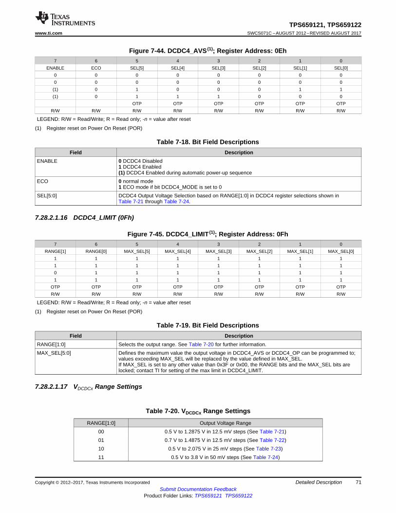
71
TPS659121, TPS659122www.ti.com SWCS071C –AUGUST 2012–REVISED AUGUST 2017
Submit Documentation FeedbackProduct Folder Links: TPS659121 TPS659122
Detailed DescriptionCopyright © 2012–2017, Texas Instruments Incorporated
(1) Register reset on Power On Reset (POR)
Figure 7-44. DCDC4_AVS (1); Register Address: 0Eh7 6 5 4 3 2 1 0
ENABLE ECO SEL[5] SEL[4] SEL[3] SEL[2] SEL[1] SEL[0]0 0 0 0 0 0 0 00 0 0 0 0 0 0 0
(1) 0 1 0 0 0 1 1(1) 0 1 1 1 0 0 0
OTP OTP OTP OTP OTP OTPR/W R/W R/W R/W R/W R/W R/W R/W
LEGEND: R/W = Read/Write; R = Read only; -n = value after reset
Table 7-18. Bit Field DescriptionsField Description
ENABLE 0 DCDC4 Disabled1 DCDC4 Enabled(1) DCDC4 Enabled during automatic power-up sequence
ECO 0 normal mode1 ECO mode if bit DCDC4_MODE is set to 0
SEL[5:0] DCDC4 Output Voltage Selection based on RANGE[1:0] in DCDC4 register selections shown inTable 7-21 through Table 7-24.
7.28.2.1.16 DCDC4_LIMIT (0Fh)
(1) Register reset on Power On Reset (POR)
Figure 7-45. DCDC4_LIMIT (1); Register Address: 0Fh7 6 5 4 3 2 1 0
RANGE[1] RANGE[0] MAX_SEL[5] MAX_SEL[4] MAX_SEL[3] MAX_SEL[2] MAX_SEL[1] MAX_SEL[0]1 1 1 1 1 1 1 11 1 1 1 1 1 1 10 1 1 1 1 1 1 11 1 1 1 1 1 1 1
OTP OTP OTP OTP OTP OTP OTP OTPR/W R/W R/W R/W R/W R/W R/W R/W
LEGEND: R/W = Read/Write; R = Read only; -n = value after reset
Table 7-19. Bit Field DescriptionsField Description
RANGE[1:0] Selects the output range. See Table 7-20 for further information.MAX_SEL[5:0] Defines the maximum value the output voltage in DCDC4_AVS or DCDC4_OP can be programmed to;
values exceeding MAX_SEL will be replaced by the value defined in MAX_SEL.If MAX_SEL is set to any other value than 0x3F or 0x00, the RANGE bits and the MAX_SEL bits arelocked; contact TI for setting of the max limit in DCDC4_LIMIT.
7.28.2.1.17 VDCDCx Range Settings
Table 7-20. VDCDCx Range Settings
RANGE[1:0] Output Voltage Range00 0.5 V to 1.2875 V in 12.5 mV steps (See Table 7-21)01 0.7 V to 1.4875 V in 12.5 mV steps (See Table 7-22)10 0.5 V to 2.075 V in 25 mV steps (See Table 7-23)11 0.5 V to 3.8 V in 50 mV steps (See Table 7-24)
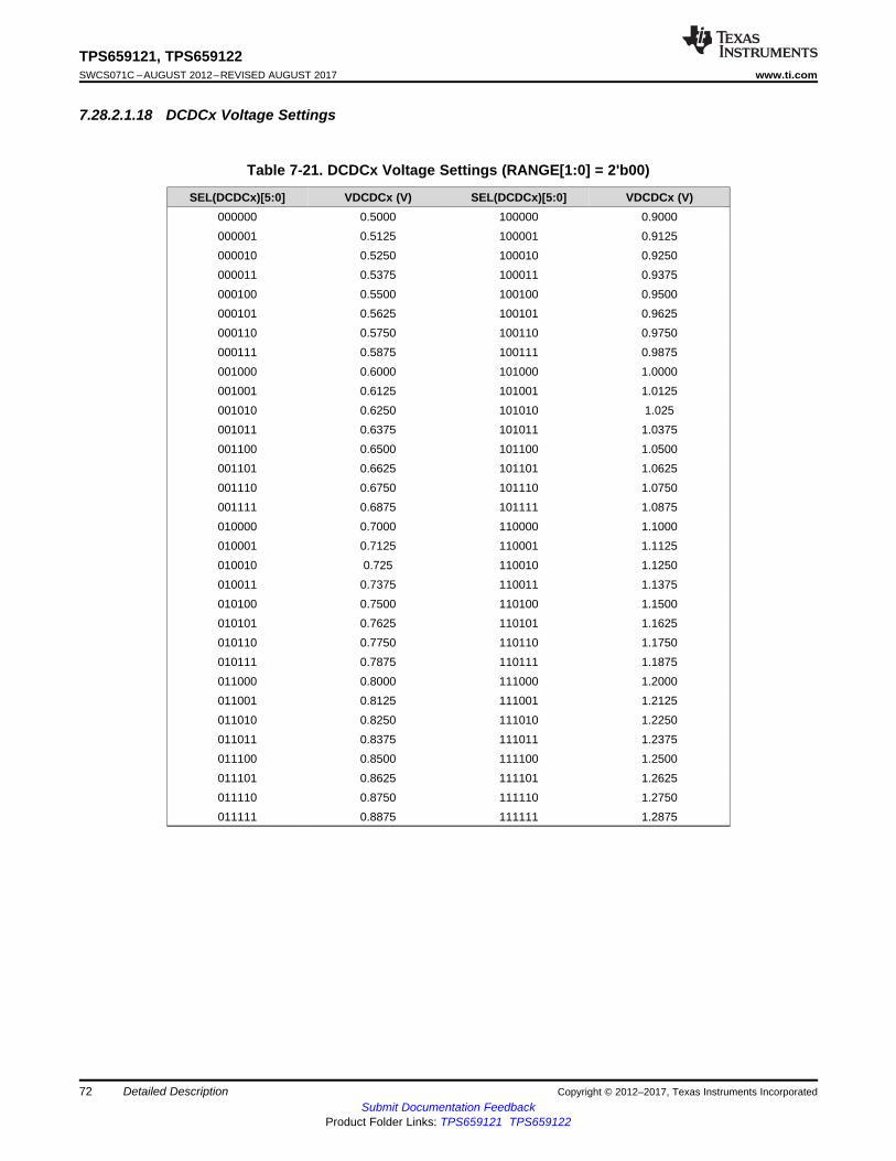
72
TPS659121, TPS659122SWCS071C –AUGUST 2012–REVISED AUGUST 2017 www.ti.com
Submit Documentation FeedbackProduct Folder Links: TPS659121 TPS659122
Detailed Description Copyright © 2012–2017, Texas Instruments Incorporated
7.28.2.1.18 DCDCx Voltage Settings
Table 7-21. DCDCx Voltage Settings (RANGE[1:0] = 2'b00)
SEL(DCDCx)[5:0] VDCDCx (V) SEL(DCDCx)[5:0] VDCDCx (V)000000 0.5000 100000 0.9000000001 0.5125 100001 0.9125000010 0.5250 100010 0.9250000011 0.5375 100011 0.9375000100 0.5500 100100 0.9500000101 0.5625 100101 0.9625000110 0.5750 100110 0.9750000111 0.5875 100111 0.9875001000 0.6000 101000 1.0000001001 0.6125 101001 1.0125001010 0.6250 101010 1.025001011 0.6375 101011 1.0375001100 0.6500 101100 1.0500001101 0.6625 101101 1.0625001110 0.6750 101110 1.0750001111 0.6875 101111 1.0875010000 0.7000 110000 1.1000010001 0.7125 110001 1.1125010010 0.725 110010 1.1250010011 0.7375 110011 1.1375010100 0.7500 110100 1.1500010101 0.7625 110101 1.1625010110 0.7750 110110 1.1750010111 0.7875 110111 1.1875011000 0.8000 111000 1.2000011001 0.8125 111001 1.2125011010 0.8250 111010 1.2250011011 0.8375 111011 1.2375011100 0.8500 111100 1.2500011101 0.8625 111101 1.2625011110 0.8750 111110 1.2750011111 0.8875 111111 1.2875
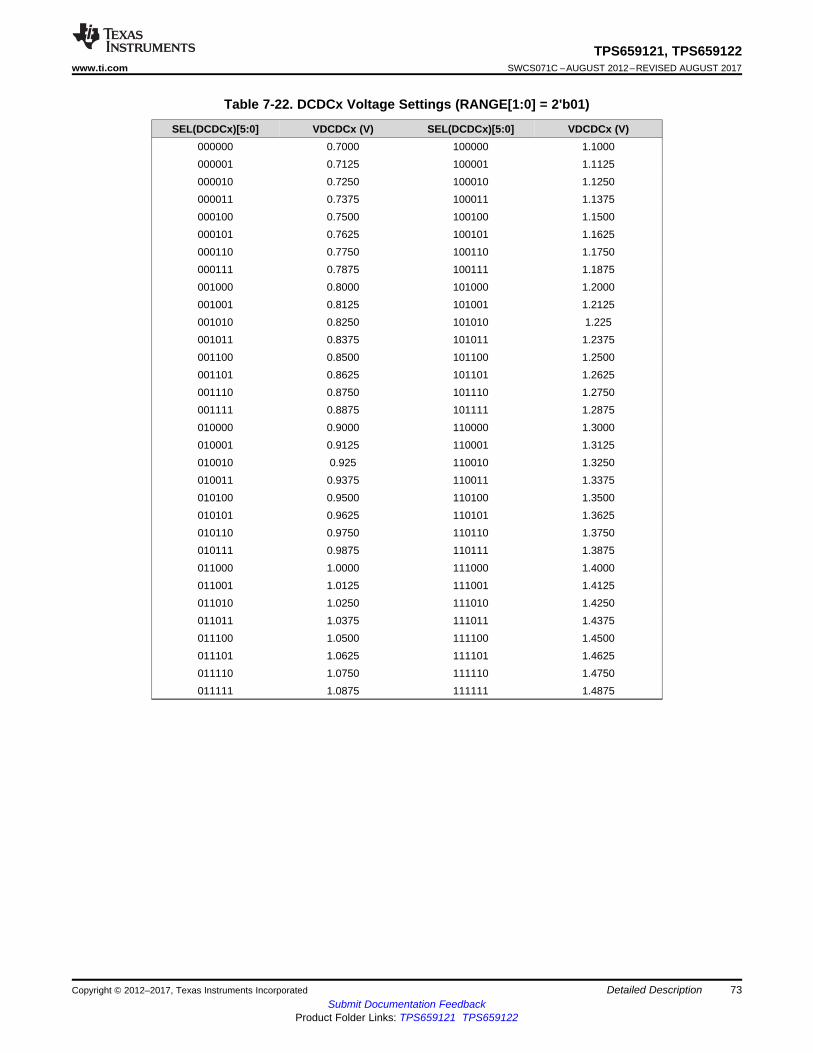
73
TPS659121, TPS659122www.ti.com SWCS071C –AUGUST 2012–REVISED AUGUST 2017
Submit Documentation FeedbackProduct Folder Links: TPS659121 TPS659122
Detailed DescriptionCopyright © 2012–2017, Texas Instruments Incorporated
Table 7-22. DCDCx Voltage Settings (RANGE[1:0] = 2'b01)
SEL(DCDCx)[5:0] VDCDCx (V) SEL(DCDCx)[5:0] VDCDCx (V)000000 0.7000 100000 1.1000000001 0.7125 100001 1.1125000010 0.7250 100010 1.1250000011 0.7375 100011 1.1375000100 0.7500 100100 1.1500000101 0.7625 100101 1.1625000110 0.7750 100110 1.1750000111 0.7875 100111 1.1875001000 0.8000 101000 1.2000001001 0.8125 101001 1.2125001010 0.8250 101010 1.225001011 0.8375 101011 1.2375001100 0.8500 101100 1.2500001101 0.8625 101101 1.2625001110 0.8750 101110 1.2750001111 0.8875 101111 1.2875010000 0.9000 110000 1.3000010001 0.9125 110001 1.3125010010 0.925 110010 1.3250010011 0.9375 110011 1.3375010100 0.9500 110100 1.3500010101 0.9625 110101 1.3625010110 0.9750 110110 1.3750010111 0.9875 110111 1.3875011000 1.0000 111000 1.4000011001 1.0125 111001 1.4125011010 1.0250 111010 1.4250011011 1.0375 111011 1.4375011100 1.0500 111100 1.4500011101 1.0625 111101 1.4625011110 1.0750 111110 1.4750011111 1.0875 111111 1.4875
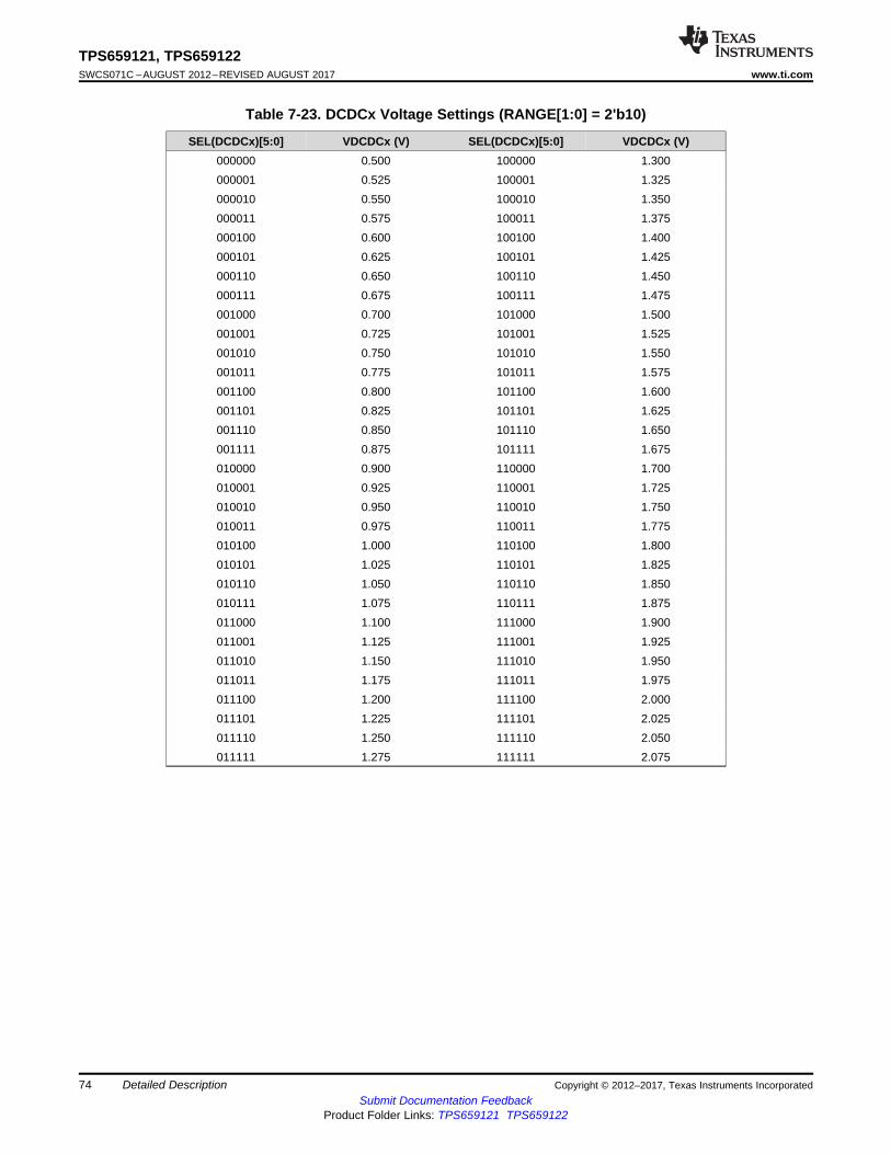
74
TPS659121, TPS659122SWCS071C –AUGUST 2012–REVISED AUGUST 2017 www.ti.com
Submit Documentation FeedbackProduct Folder Links: TPS659121 TPS659122
Detailed Description Copyright © 2012–2017, Texas Instruments Incorporated
Table 7-23. DCDCx Voltage Settings (RANGE[1:0] = 2'b10)
SEL(DCDCx)[5:0] VDCDCx (V) SEL(DCDCx)[5:0] VDCDCx (V)000000 0.500 100000 1.300000001 0.525 100001 1.325000010 0.550 100010 1.350000011 0.575 100011 1.375000100 0.600 100100 1.400000101 0.625 100101 1.425000110 0.650 100110 1.450000111 0.675 100111 1.475001000 0.700 101000 1.500001001 0.725 101001 1.525001010 0.750 101010 1.550001011 0.775 101011 1.575001100 0.800 101100 1.600001101 0.825 101101 1.625001110 0.850 101110 1.650001111 0.875 101111 1.675010000 0.900 110000 1.700010001 0.925 110001 1.725010010 0.950 110010 1.750010011 0.975 110011 1.775010100 1.000 110100 1.800010101 1.025 110101 1.825010110 1.050 110110 1.850010111 1.075 110111 1.875011000 1.100 111000 1.900011001 1.125 111001 1.925011010 1.150 111010 1.950011011 1.175 111011 1.975011100 1.200 111100 2.000011101 1.225 111101 2.025011110 1.250 111110 2.050011111 1.275 111111 2.075
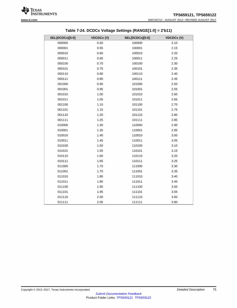
75
TPS659121, TPS659122www.ti.com SWCS071C –AUGUST 2012–REVISED AUGUST 2017
Submit Documentation FeedbackProduct Folder Links: TPS659121 TPS659122
Detailed DescriptionCopyright © 2012–2017, Texas Instruments Incorporated
Table 7-24. DCDCx Voltage Settings (RANGE[1:0] = 2'b11)
SEL(DCDCx)[5:0] VDCDCx (V) SEL(DCDCx)[5:0] VDCDCx (V)000000 0.50 100000 2.10000001 0.55 100001 2.15000010 0.60 100010 2.20000011 0.65 100011 2.25000100 0.70 100100 2.30000101 0.75 100101 2.35000110 0.80 100110 2.40000111 0.85 100111 2.45001000 0.90 101000 2.50001001 0.95 101001 2.55001010 1.00 101010 2.60001011 1.05 101011 2.65001100 1.10 101100 2.70001101 1.15 101101 2.75001110 1.20 101110 2.80001111 1.25 101111 2.85010000 1.30 110000 2.90010001 1.35 110001 2.95010010 1.40 110010 3.00010011 1.45 110011 3.05010100 1.50 110100 3.10010101 1.55 110101 3.15010110 1.60 110110 3.20010111 1.65 110111 3.25011000 1.70 111000 3.30011001 1.75 111001 3.35011010 1.80 111010 3.40011011 1.85 111011 3.45011100 1.90 111100 3.50011101 1.95 111101 3.55011110 2.00 111110 3.60011111 2.05 111111 3.80
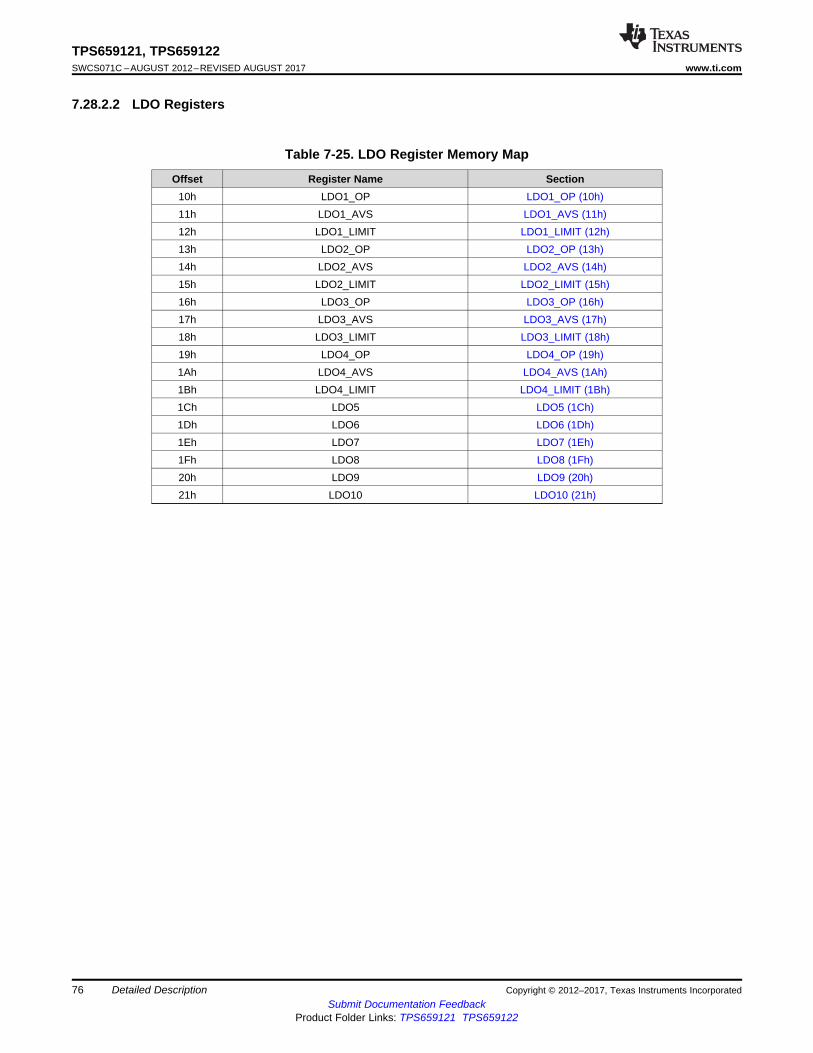
76
TPS659121, TPS659122SWCS071C –AUGUST 2012–REVISED AUGUST 2017 www.ti.com
Submit Documentation FeedbackProduct Folder Links: TPS659121 TPS659122
Detailed Description Copyright © 2012–2017, Texas Instruments Incorporated
7.28.2.2 LDO Registers
Table 7-25. LDO Register Memory Map
Offset Register Name Section10h LDO1_OP LDO1_OP (10h)11h LDO1_AVS LDO1_AVS (11h)12h LDO1_LIMIT LDO1_LIMIT (12h)13h LDO2_OP LDO2_OP (13h)14h LDO2_AVS LDO2_AVS (14h)15h LDO2_LIMIT LDO2_LIMIT (15h)16h LDO3_OP LDO3_OP (16h)17h LDO3_AVS LDO3_AVS (17h)18h LDO3_LIMIT LDO3_LIMIT (18h)19h LDO4_OP LDO4_OP (19h)1Ah LDO4_AVS LDO4_AVS (1Ah)1Bh LDO4_LIMIT LDO4_LIMIT (1Bh)1Ch LDO5 LDO5 (1Ch)1Dh LDO6 LDO6 (1Dh)1Eh LDO7 LDO7 (1Eh)1Fh LDO8 LDO8 (1Fh)20h LDO9 LDO9 (20h)21h LDO10 LDO10 (21h)
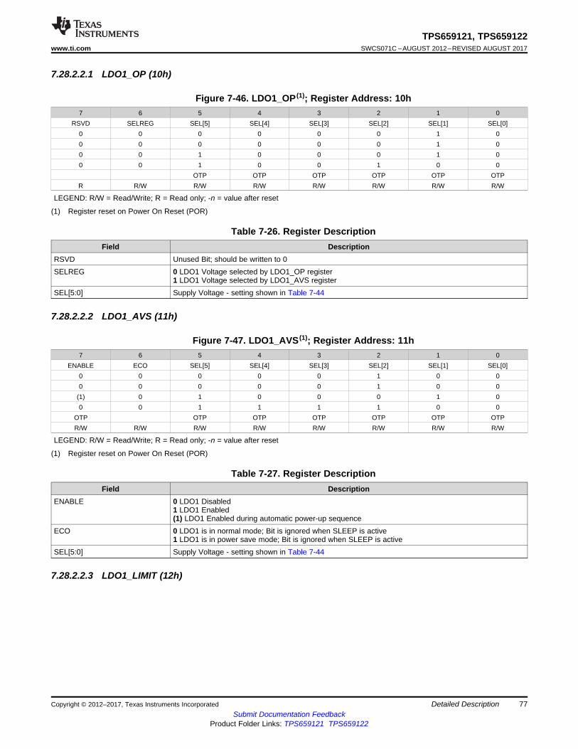
77
TPS659121, TPS659122www.ti.com SWCS071C –AUGUST 2012–REVISED AUGUST 2017
Submit Documentation FeedbackProduct Folder Links: TPS659121 TPS659122
Detailed DescriptionCopyright © 2012–2017, Texas Instruments Incorporated
7.28.2.2.1 LDO1_OP (10h)
(1) Register reset on Power On Reset (POR)
Figure 7-46. LDO1_OP (1); Register Address: 10h7 6 5 4 3 2 1 0
RSVD SELREG SEL[5] SEL[4] SEL[3] SEL[2] SEL[1] SEL[0]0 0 0 0 0 0 1 00 0 0 0 0 0 1 00 0 1 0 0 0 1 00 0 1 0 0 1 0 0
OTP OTP OTP OTP OTP OTPR R/W R/W R/W R/W R/W R/W R/W
LEGEND: R/W = Read/Write; R = Read only; -n = value after reset
Table 7-26. Register DescriptionField Description
RSVD Unused Bit; should be written to 0SELREG 0 LDO1 Voltage selected by LDO1_OP register
1 LDO1 Voltage selected by LDO1_AVS registerSEL[5:0] Supply Voltage - setting shown in Table 7-44
7.28.2.2.2 LDO1_AVS (11h)
(1) Register reset on Power On Reset (POR)
Figure 7-47. LDO1_AVS (1); Register Address: 11h7 6 5 4 3 2 1 0
ENABLE ECO SEL[5] SEL[4] SEL[3] SEL[2] SEL[1] SEL[0]0 0 0 0 0 1 0 00 0 0 0 0 1 0 0
(1) 0 1 0 0 0 1 00 0 1 1 1 1 0 0
OTP OTP OTP OTP OTP OTP OTPR/W R/W R/W R/W R/W R/W R/W R/W
LEGEND: R/W = Read/Write; R = Read only; -n = value after reset
Table 7-27. Register DescriptionField Description
ENABLE 0 LDO1 Disabled1 LDO1 Enabled(1) LDO1 Enabled during automatic power-up sequence
ECO 0 LDO1 is in normal mode; Bit is ignored when SLEEP is active1 LDO1 is in power save mode; Bit is ignored when SLEEP is active
SEL[5:0] Supply Voltage - setting shown in Table 7-44
7.28.2.2.3 LDO1_LIMIT (12h)
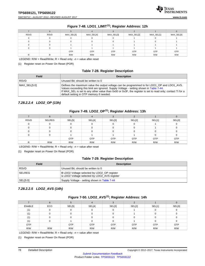
78
TPS659121, TPS659122SWCS071C –AUGUST 2012–REVISED AUGUST 2017 www.ti.com
Submit Documentation FeedbackProduct Folder Links: TPS659121 TPS659122
Detailed Description Copyright © 2012–2017, Texas Instruments Incorporated
(1) Register reset on Power On Reset (POR)
Figure 7-48. LDO1_LIMIT (1); Register Address: 12h7 6 5 4 3 2 1 0
RSVD RSVD MAX_SEL[5] MAX_SEL[4] MAX_SEL[3] MAX_SEL[2] MAX_SEL[1] MAX_SEL[0]
0 0 0 0 0 1 0 1
0 0 0 0 0 1 0 1
0 0 1 1 1 1 1 1
0 0 1 1 1 1 1 1
OTP OTP OTP OTP OTP OTP
R R R/W R/W R/W R/W R/W R/W
LEGEND: R/W = Read/Write; R = Read only; -n = value after reset
Table 7-28. Register DescriptionField Description
RSVD Unused Bit; should be written to 0MAX_SEL[5:0] Defines the maximum value the output voltage can be programmed to for LDO1_OP and LDO1_AVS.
Values exceeding this limit are ignored. Supply Voltage - setting shown in Table 7-44.If MAX_SEL is set to any other value than 0x00 or 0x3F, the register is set to read only; contact Ti for adefault setting in OTP memory if needed.
7.28.2.2.4 LDO2_OP (13h)
(1) Register reset on Power On Reset (POR)
Figure 7-49. LDO2_OP (1); Register Address: 13h7 6 5 4 3 2 1 0
RSVD SELREG SEL[5] SEL[4] SEL[3] SEL[2] SEL[1] SEL[0]0 0 0 0 0 0 1 00 0 0 0 0 0 1 00 0 0 0 0 0 0 00 0 1 1 1 1 0 0
OTP OTP OTP OTP OTP OTPR R/W R/W R/W R/W R/W R/W R/W
LEGEND: R/W = Read/Write; R = Read only; -n = value after reset
Table 7-29. Register DescriptionField Description
RSVD Unused Bit; should be written to 0SELREG 0 LDO2 Voltage selected by LDO2_OP register
1 LDO2 Voltage selected by LDO2_AVS registerSEL[5:0] Supply Voltage - setting shown in Table 7-44
7.28.2.2.5 LDO2_AVS (14h)
(1) Register reset on Power On Reset (POR)
Figure 7-50. LDO2_AVS (1); Register Address: 14h7 6 5 4 3 2 1 0
ENABLE ECO SEL[5] SEL[4] SEL[3] SEL[2] SEL[1] SEL[0](1) 0 0 0 0 1 0 0(1) 0 0 0 0 1 0 0(1) 0 0 0 0 0 0 0(1) 0 1 0 0 1 0 0
OTP OTP OTP OTP OTP OTP OTPR/W R/W R/W R/W R/W R/W R/W R/W
LEGEND: R/W = Read/Write; R = Read only; -n = value after reset
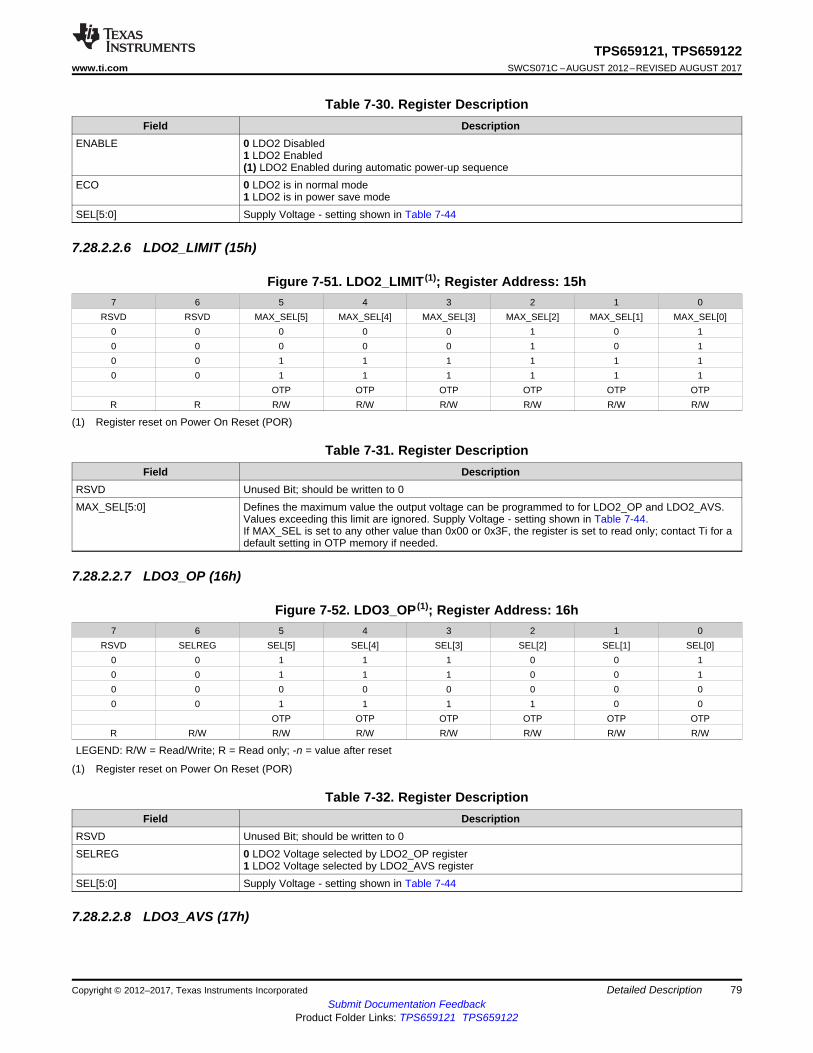
79
TPS659121, TPS659122www.ti.com SWCS071C –AUGUST 2012–REVISED AUGUST 2017
Submit Documentation FeedbackProduct Folder Links: TPS659121 TPS659122
Detailed DescriptionCopyright © 2012–2017, Texas Instruments Incorporated
Table 7-30. Register DescriptionField Description
ENABLE 0 LDO2 Disabled1 LDO2 Enabled(1) LDO2 Enabled during automatic power-up sequence
ECO 0 LDO2 is in normal mode1 LDO2 is in power save mode
SEL[5:0] Supply Voltage - setting shown in Table 7-44
7.28.2.2.6 LDO2_LIMIT (15h)
(1) Register reset on Power On Reset (POR)
Figure 7-51. LDO2_LIMIT (1); Register Address: 15h7 6 5 4 3 2 1 0
RSVD RSVD MAX_SEL[5] MAX_SEL[4] MAX_SEL[3] MAX_SEL[2] MAX_SEL[1] MAX_SEL[0]0 0 0 0 0 1 0 10 0 0 0 0 1 0 10 0 1 1 1 1 1 10 0 1 1 1 1 1 1
OTP OTP OTP OTP OTP OTPR R R/W R/W R/W R/W R/W R/W
Table 7-31. Register DescriptionField Description
RSVD Unused Bit; should be written to 0MAX_SEL[5:0] Defines the maximum value the output voltage can be programmed to for LDO2_OP and LDO2_AVS.
Values exceeding this limit are ignored. Supply Voltage - setting shown in Table 7-44.If MAX_SEL is set to any other value than 0x00 or 0x3F, the register is set to read only; contact Ti for adefault setting in OTP memory if needed.
7.28.2.2.7 LDO3_OP (16h)
(1) Register reset on Power On Reset (POR)
Figure 7-52. LDO3_OP (1); Register Address: 16h7 6 5 4 3 2 1 0
RSVD SELREG SEL[5] SEL[4] SEL[3] SEL[2] SEL[1] SEL[0]0 0 1 1 1 0 0 10 0 1 1 1 0 0 10 0 0 0 0 0 0 00 0 1 1 1 1 0 0
OTP OTP OTP OTP OTP OTPR R/W R/W R/W R/W R/W R/W R/W
LEGEND: R/W = Read/Write; R = Read only; -n = value after reset
Table 7-32. Register DescriptionField Description
RSVD Unused Bit; should be written to 0SELREG 0 LDO2 Voltage selected by LDO2_OP register
1 LDO2 Voltage selected by LDO2_AVS registerSEL[5:0] Supply Voltage - setting shown in Table 7-44
7.28.2.2.8 LDO3_AVS (17h)
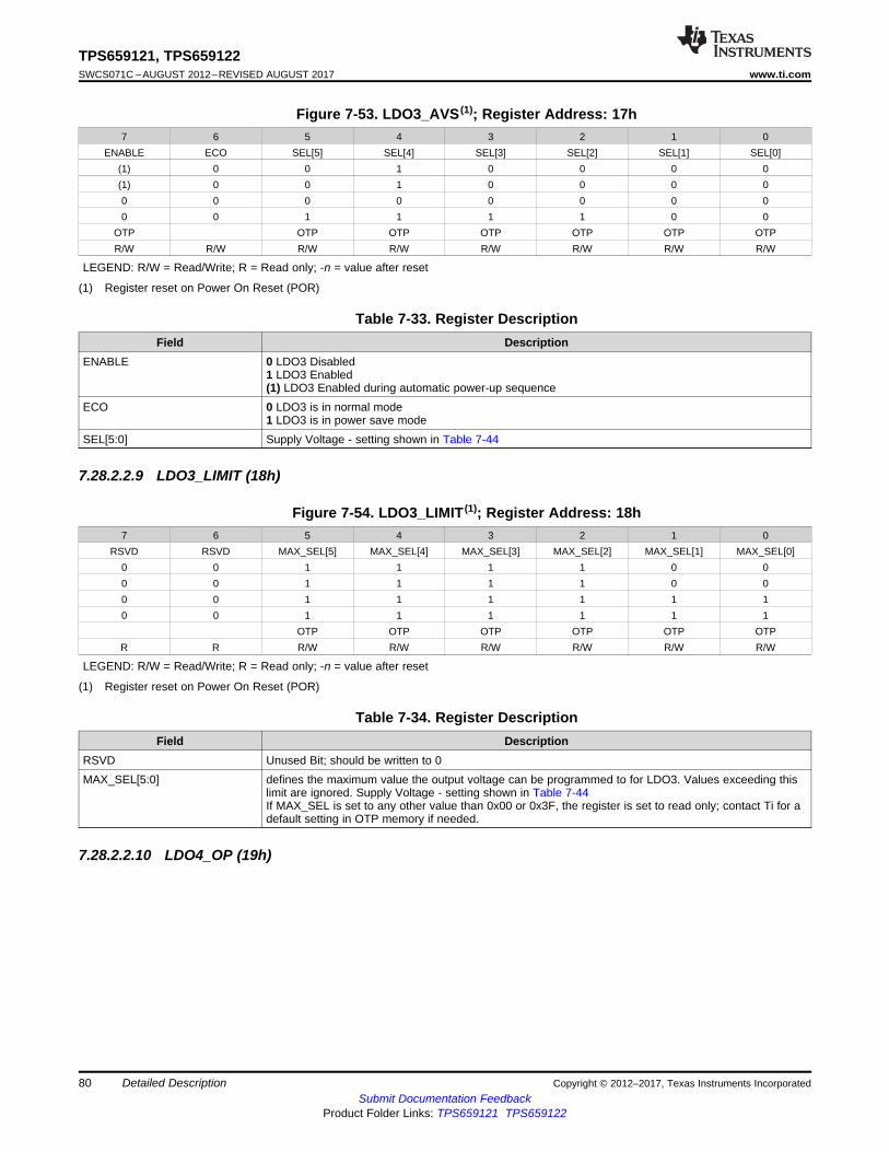
80
TPS659121, TPS659122SWCS071C –AUGUST 2012–REVISED AUGUST 2017 www.ti.com
Submit Documentation FeedbackProduct Folder Links: TPS659121 TPS659122
Detailed Description Copyright © 2012–2017, Texas Instruments Incorporated
(1) Register reset on Power On Reset (POR)
Figure 7-53. LDO3_AVS (1); Register Address: 17h7 6 5 4 3 2 1 0
ENABLE ECO SEL[5] SEL[4] SEL[3] SEL[2] SEL[1] SEL[0](1) 0 0 1 0 0 0 0(1) 0 0 1 0 0 0 00 0 0 0 0 0 0 00 0 1 1 1 1 0 0
OTP OTP OTP OTP OTP OTP OTPR/W R/W R/W R/W R/W R/W R/W R/W
LEGEND: R/W = Read/Write; R = Read only; -n = value after reset
Table 7-33. Register DescriptionField Description
ENABLE 0 LDO3 Disabled1 LDO3 Enabled(1) LDO3 Enabled during automatic power-up sequence
ECO 0 LDO3 is in normal mode1 LDO3 is in power save mode
SEL[5:0] Supply Voltage - setting shown in Table 7-44
7.28.2.2.9 LDO3_LIMIT (18h)
(1) Register reset on Power On Reset (POR)
Figure 7-54. LDO3_LIMIT (1); Register Address: 18h7 6 5 4 3 2 1 0
RSVD RSVD MAX_SEL[5] MAX_SEL[4] MAX_SEL[3] MAX_SEL[2] MAX_SEL[1] MAX_SEL[0]0 0 1 1 1 1 0 00 0 1 1 1 1 0 00 0 1 1 1 1 1 10 0 1 1 1 1 1 1
OTP OTP OTP OTP OTP OTPR R R/W R/W R/W R/W R/W R/W
LEGEND: R/W = Read/Write; R = Read only; -n = value after reset
Table 7-34. Register DescriptionField Description
RSVD Unused Bit; should be written to 0MAX_SEL[5:0] defines the maximum value the output voltage can be programmed to for LDO3. Values exceeding this
limit are ignored. Supply Voltage - setting shown in Table 7-44If MAX_SEL is set to any other value than 0x00 or 0x3F, the register is set to read only; contact Ti for adefault setting in OTP memory if needed.
7.28.2.2.10 LDO4_OP (19h)
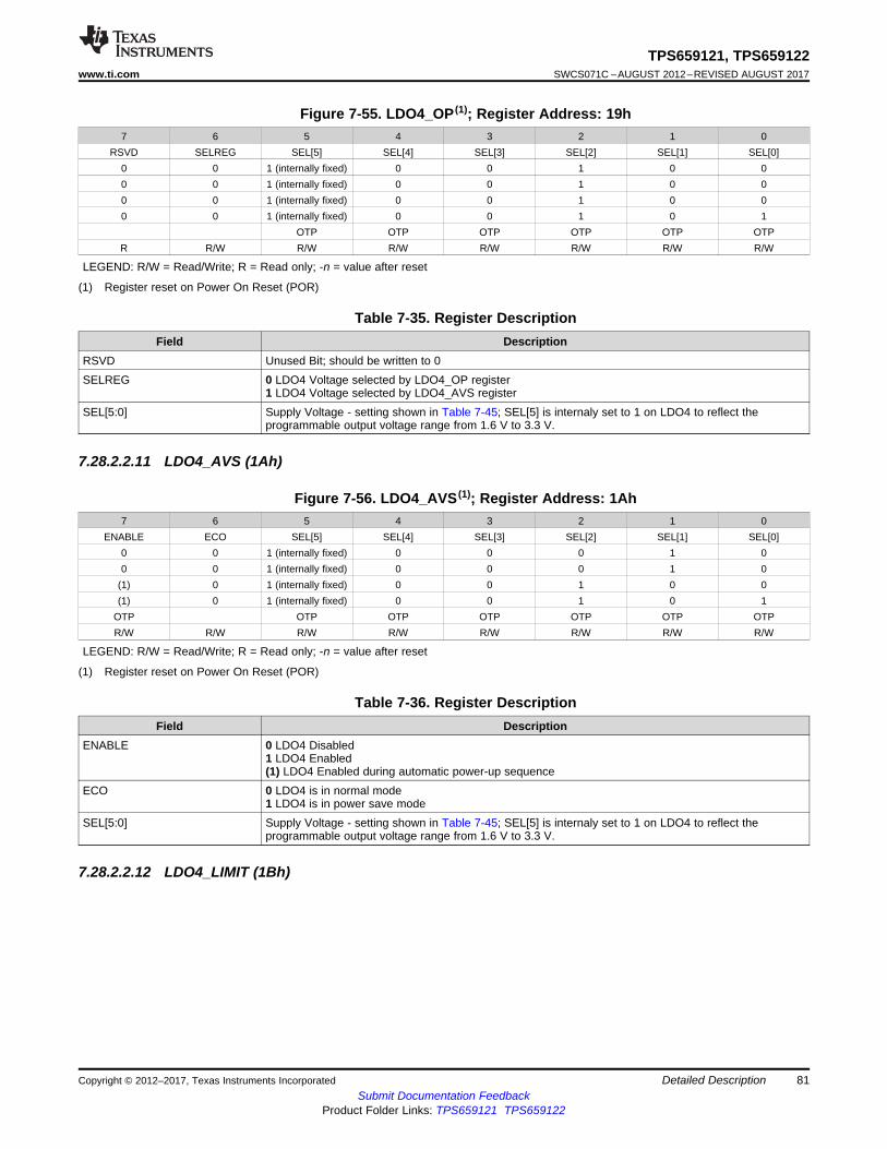
81
TPS659121, TPS659122www.ti.com SWCS071C –AUGUST 2012–REVISED AUGUST 2017
Submit Documentation FeedbackProduct Folder Links: TPS659121 TPS659122
Detailed DescriptionCopyright © 2012–2017, Texas Instruments Incorporated
(1) Register reset on Power On Reset (POR)
Figure 7-55. LDO4_OP (1); Register Address: 19h7 6 5 4 3 2 1 0
RSVD SELREG SEL[5] SEL[4] SEL[3] SEL[2] SEL[1] SEL[0]0 0 1 (internally fixed) 0 0 1 0 00 0 1 (internally fixed) 0 0 1 0 00 0 1 (internally fixed) 0 0 1 0 00 0 1 (internally fixed) 0 0 1 0 1
OTP OTP OTP OTP OTP OTPR R/W R/W R/W R/W R/W R/W R/W
LEGEND: R/W = Read/Write; R = Read only; -n = value after reset
Table 7-35. Register DescriptionField Description
RSVD Unused Bit; should be written to 0SELREG 0 LDO4 Voltage selected by LDO4_OP register
1 LDO4 Voltage selected by LDO4_AVS registerSEL[5:0] Supply Voltage - setting shown in Table 7-45; SEL[5] is internaly set to 1 on LDO4 to reflect the
programmable output voltage range from 1.6 V to 3.3 V.
7.28.2.2.11 LDO4_AVS (1Ah)
(1) Register reset on Power On Reset (POR)
Figure 7-56. LDO4_AVS (1); Register Address: 1Ah7 6 5 4 3 2 1 0
ENABLE ECO SEL[5] SEL[4] SEL[3] SEL[2] SEL[1] SEL[0]0 0 1 (internally fixed) 0 0 0 1 00 0 1 (internally fixed) 0 0 0 1 0
(1) 0 1 (internally fixed) 0 0 1 0 0(1) 0 1 (internally fixed) 0 0 1 0 1
OTP OTP OTP OTP OTP OTP OTPR/W R/W R/W R/W R/W R/W R/W R/W
LEGEND: R/W = Read/Write; R = Read only; -n = value after reset
Table 7-36. Register DescriptionField Description
ENABLE 0 LDO4 Disabled1 LDO4 Enabled(1) LDO4 Enabled during automatic power-up sequence
ECO 0 LDO4 is in normal mode1 LDO4 is in power save mode
SEL[5:0] Supply Voltage - setting shown in Table 7-45; SEL[5] is internaly set to 1 on LDO4 to reflect theprogrammable output voltage range from 1.6 V to 3.3 V.
7.28.2.2.12 LDO4_LIMIT (1Bh)
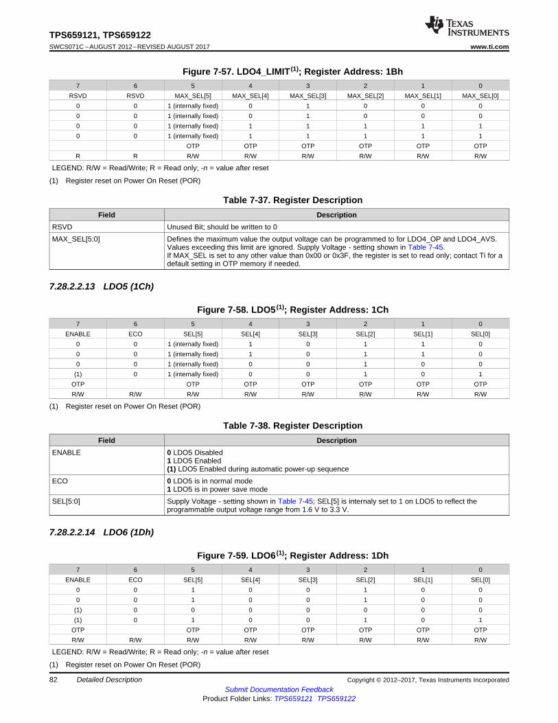
82
TPS659121, TPS659122SWCS071C –AUGUST 2012–REVISED AUGUST 2017 www.ti.com
Submit Documentation FeedbackProduct Folder Links: TPS659121 TPS659122
Detailed Description Copyright © 2012–2017, Texas Instruments Incorporated
(1) Register reset on Power On Reset (POR)
Figure 7-57. LDO4_LIMIT (1); Register Address: 1Bh7 6 5 4 3 2 1 0
RSVD RSVD MAX_SEL[5] MAX_SEL[4] MAX_SEL[3] MAX_SEL[2] MAX_SEL[1] MAX_SEL[0]0 0 1 (internally fixed) 0 1 0 0 00 0 1 (internally fixed) 0 1 0 0 00 0 1 (internally fixed) 1 1 1 1 10 0 1 (internally fixed) 1 1 1 1 1
OTP OTP OTP OTP OTP OTPR R R/W R/W R/W R/W R/W R/W
LEGEND: R/W = Read/Write; R = Read only; -n = value after reset
Table 7-37. Register DescriptionField Description
RSVD Unused Bit; should be written to 0MAX_SEL[5:0] Defines the maximum value the output voltage can be programmed to for LDO4_OP and LDO4_AVS.
Values exceeding this limit are ignored. Supply Voltage - setting shown in Table 7-45.If MAX_SEL is set to any other value than 0x00 or 0x3F, the register is set to read only; contact Ti for adefault setting in OTP memory if needed.
7.28.2.2.13 LDO5 (1Ch)
(1) Register reset on Power On Reset (POR)
Figure 7-58. LDO5 (1); Register Address: 1Ch7 6 5 4 3 2 1 0
ENABLE ECO SEL[5] SEL[4] SEL[3] SEL[2] SEL[1] SEL[0]0 0 1 (internally fixed) 1 0 1 1 00 0 1 (internally fixed) 1 0 1 1 00 0 1 (internally fixed) 0 0 1 0 0
(1) 0 1 (internally fixed) 0 0 1 0 1OTP OTP OTP OTP OTP OTP OTPR/W R/W R/W R/W R/W R/W R/W R/W
Table 7-38. Register DescriptionField Description
ENABLE 0 LDO5 Disabled1 LDO5 Enabled(1) LDO5 Enabled during automatic power-up sequence
ECO 0 LDO5 is in normal mode1 LDO5 is in power save mode
SEL[5:0] Supply Voltage - setting shown in Table 7-45; SEL[5] is internaly set to 1 on LDO5 to reflect theprogrammable output voltage range from 1.6 V to 3.3 V.
7.28.2.2.14 LDO6 (1Dh)
(1) Register reset on Power On Reset (POR)
Figure 7-59. LDO6 (1); Register Address: 1Dh7 6 5 4 3 2 1 0
ENABLE ECO SEL[5] SEL[4] SEL[3] SEL[2] SEL[1] SEL[0]0 0 1 0 0 1 0 00 0 1 0 0 1 0 0
(1) 0 0 0 0 0 0 0(1) 0 1 0 0 1 0 1
OTP OTP OTP OTP OTP OTP OTPR/W R/W R/W R/W R/W R/W R/W R/W
LEGEND: R/W = Read/Write; R = Read only; -n = value after reset
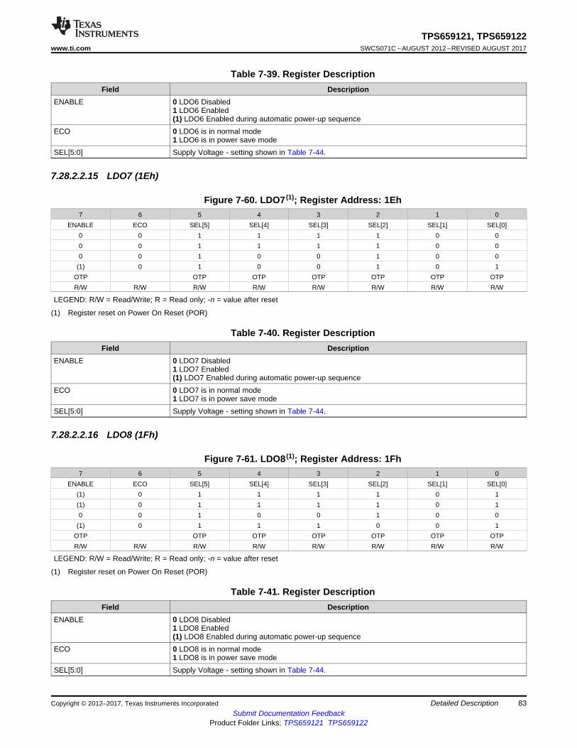
83
TPS659121, TPS659122www.ti.com SWCS071C –AUGUST 2012–REVISED AUGUST 2017
Submit Documentation FeedbackProduct Folder Links: TPS659121 TPS659122
Detailed DescriptionCopyright © 2012–2017, Texas Instruments Incorporated
Table 7-39. Register DescriptionField Description
ENABLE 0 LDO6 Disabled1 LDO6 Enabled(1) LDO6 Enabled during automatic power-up sequence
ECO 0 LDO6 is in normal mode1 LDO6 is in power save mode
SEL[5:0] Supply Voltage - setting shown in Table 7-44.
7.28.2.2.15 LDO7 (1Eh)
(1) Register reset on Power On Reset (POR)
Figure 7-60. LDO7 (1); Register Address: 1Eh7 6 5 4 3 2 1 0
ENABLE ECO SEL[5] SEL[4] SEL[3] SEL[2] SEL[1] SEL[0]0 0 1 1 1 1 0 00 0 1 1 1 1 0 00 0 1 0 0 1 0 0
(1) 0 1 0 0 1 0 1OTP OTP OTP OTP OTP OTP OTPR/W R/W R/W R/W R/W R/W R/W R/W
LEGEND: R/W = Read/Write; R = Read only; -n = value after reset
Table 7-40. Register DescriptionField Description
ENABLE 0 LDO7 Disabled1 LDO7 Enabled(1) LDO7 Enabled during automatic power-up sequence
ECO 0 LDO7 is in normal mode1 LDO7 is in power save mode
SEL[5:0] Supply Voltage - setting shown in Table 7-44.
7.28.2.2.16 LDO8 (1Fh)
(1) Register reset on Power On Reset (POR)
Figure 7-61. LDO8 (1); Register Address: 1Fh7 6 5 4 3 2 1 0
ENABLE ECO SEL[5] SEL[4] SEL[3] SEL[2] SEL[1] SEL[0](1) 0 1 1 1 1 0 1(1) 0 1 1 1 1 0 10 0 1 0 0 1 0 0
(1) 0 1 1 1 0 0 1OTP OTP OTP OTP OTP OTP OTPR/W R/W R/W R/W R/W R/W R/W R/W
LEGEND: R/W = Read/Write; R = Read only; -n = value after reset
Table 7-41. Register DescriptionField Description
ENABLE 0 LDO8 Disabled1 LDO8 Enabled(1) LDO8 Enabled during automatic power-up sequence
ECO 0 LDO8 is in normal mode1 LDO8 is in power save mode
SEL[5:0] Supply Voltage - setting shown in Table 7-44.
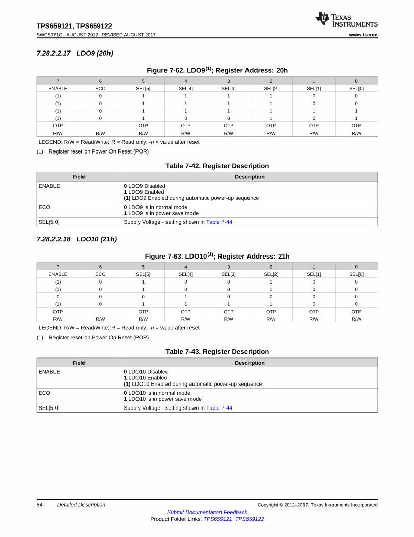
84
TPS659121, TPS659122SWCS071C –AUGUST 2012–REVISED AUGUST 2017 www.ti.com
Submit Documentation FeedbackProduct Folder Links: TPS659121 TPS659122
Detailed Description Copyright © 2012–2017, Texas Instruments Incorporated
7.28.2.2.17 LDO9 (20h)
(1) Register reset on Power On Reset (POR)
Figure 7-62. LDO9 (1); Register Address: 20h7 6 5 4 3 2 1 0
ENABLE ECO SEL[5] SEL[4] SEL[3] SEL[2] SEL[1] SEL[0](1) 0 1 1 1 1 0 0(1) 0 1 1 1 1 0 0(1) 0 1 1 1 1 1 1(1) 0 1 0 0 1 0 1
OTP OTP OTP OTP OTP OTP OTPR/W R/W R/W R/W R/W R/W R/W R/W
LEGEND: R/W = Read/Write; R = Read only; -n = value after reset
Table 7-42. Register DescriptionField Description
ENABLE 0 LDO9 Disabled1 LDO9 Enabled(1) LDO9 Enabled during automatic power-up sequence
ECO 0 LDO9 is in normal mode1 LDO9 is in power save mode
SEL[5:0] Supply Voltage - setting shown in Table 7-44.
7.28.2.2.18 LDO10 (21h)
(1) Register reset on Power On Reset (POR)
Figure 7-63. LDO10 (1); Register Address: 21h7 6 5 4 3 2 1 0
ENABLE ECO SEL[5] SEL[4] SEL[3] SEL[2] SEL[1] SEL[0](1) 0 1 0 0 1 0 0(1) 0 1 0 0 1 0 00 0 0 1 0 0 0 0
(1) 0 1 1 1 1 0 0OTP OTP OTP OTP OTP OTP OTPR/W R/W R/W R/W R/W R/W R/W R/W
LEGEND: R/W = Read/Write; R = Read only; -n = value after reset
Table 7-43. Register DescriptionField Description
ENABLE 0 LDO10 Disabled1 LDO10 Enabled(1) LDO10 Enabled during automatic power-up sequence
ECO 0 LDO10 is in normal mode1 LDO10 is in power save mode
SEL[5:0] Supply Voltage - setting shown in Table 7-44.
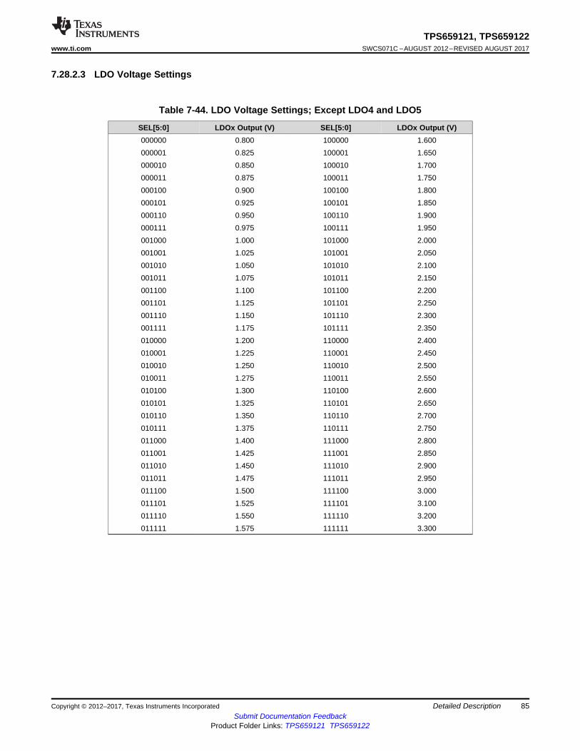
85
TPS659121, TPS659122www.ti.com SWCS071C –AUGUST 2012–REVISED AUGUST 2017
Submit Documentation FeedbackProduct Folder Links: TPS659121 TPS659122
Detailed DescriptionCopyright © 2012–2017, Texas Instruments Incorporated
7.28.2.3 LDO Voltage Settings
Table 7-44. LDO Voltage Settings; Except LDO4 and LDO5
SEL[5:0] LDOx Output (V) SEL[5:0] LDOx Output (V)000000 0.800 100000 1.600000001 0.825 100001 1.650000010 0.850 100010 1.700000011 0.875 100011 1.750000100 0.900 100100 1.800000101 0.925 100101 1.850000110 0.950 100110 1.900000111 0.975 100111 1.950001000 1.000 101000 2.000001001 1.025 101001 2.050001010 1.050 101010 2.100001011 1.075 101011 2.150001100 1.100 101100 2.200001101 1.125 101101 2.250001110 1.150 101110 2.300001111 1.175 101111 2.350010000 1.200 110000 2.400010001 1.225 110001 2.450010010 1.250 110010 2.500010011 1.275 110011 2.550010100 1.300 110100 2.600010101 1.325 110101 2.650010110 1.350 110110 2.700010111 1.375 110111 2.750011000 1.400 111000 2.800011001 1.425 111001 2.850011010 1.450 111010 2.900011011 1.475 111011 2.950011100 1.500 111100 3.000011101 1.525 111101 3.100011110 1.550 111110 3.200011111 1.575 111111 3.300
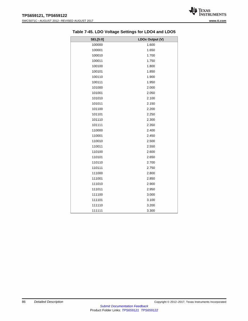
86
TPS659121, TPS659122SWCS071C –AUGUST 2012–REVISED AUGUST 2017 www.ti.com
Submit Documentation FeedbackProduct Folder Links: TPS659121 TPS659122
Detailed Description Copyright © 2012–2017, Texas Instruments Incorporated
Table 7-45. LDO Voltage Settings for LDO4 and LDO5
SEL[5:0] LDOx Output (V)100000 1.600100001 1.650100010 1.700100011 1.750100100 1.800100101 1.850100110 1.900100111 1.950101000 2.000101001 2.050101010 2.100101011 2.150101100 2.200101101 2.250101110 2.300101111 2.350110000 2.400110001 2.450110010 2.500110011 2.550110100 2.600110101 2.650110110 2.700110111 2.750111000 2.800111001 2.850111010 2.900111011 2.950111100 3.000111101 3.100111110 3.200111111 3.300
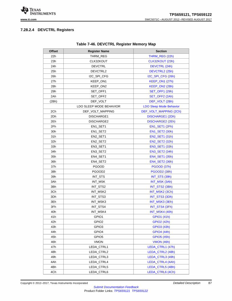
87
TPS659121, TPS659122www.ti.com SWCS071C –AUGUST 2012–REVISED AUGUST 2017
Submit Documentation FeedbackProduct Folder Links: TPS659121 TPS659122
Detailed DescriptionCopyright © 2012–2017, Texas Instruments Incorporated
7.28.2.4 DEVCTRL Registers
Table 7-46. DEVCTRL Register Memory Map
Offset Register Name Section22h THRM_REG THRM_REG (22h)23h CLK32KOUT CLK32KOUT (23h)24h DEVCTRL DEVCTRL (24h)25h DEVCTRL2 DEVCTRL2 (25h)26h I2C_SPI_CFG I2C_SPI_CFG (26h)27h KEEP_ON1 KEEP_ON1 (27h)28h KEEP_ON2 KEEP_ON2 (28h)29h SET_OFF1 SET_OFF1 (29h)2Ah SET_OFF2 SET_OFF2 (2Ah)
(2Bh) DEF_VOLT DEF_VOLT (2Bh)LDO SLEEP MODE BEHAVIOR LDO Sleep Mode Behavior
2Ch DEF_VOLT_MAPPING DEF_VOLT_MAPPING (2Ch)2Dh DISCHARGE1 DISCHARGE1 (2Dh)2Eh DISCHARGE2 DISCHARGE2 (2Eh)2Fh EN1_SET1 EN1_SET1 (2Fh)30h EN1_SET2 EN1_SET2 (30h)31h EN2_SET1 EN2_SET1 (31h)32h EN2_SET2 EN2_SET2 (32h)33h EN3_SET1 EN3_SET1 (33h)34h EN3_SET2 EN3_SET2 (34h)35h EN4_SET1 EN4_SET1 (35h)36h EN4_SET2 EN4_SET2 (36h)37h PGOOD PGOOD (37h)38h PGOOD2 PGOOD2 (38h)39h INT_STS INT_STS (39h)3Ah INT_MSK INT_MSK (3Ah)3Bh INT_STS2 INT_STS2 (3Bh)3Ch INT_MSK2 INT_MSK2 (3Ch)3Dh INT_STS3 INT_STS3 (3Dh)3Eh INT_MSK3 INT_MSK3 (3Eh)3Fh INT_STS4 INT_STS4 (3Fh)40h INT_MSK4 INT_MSK4 (40h)41h GPIO1 GPIO1 (41h)42h GPIO2 GPIO2 (42h)43h GPIO3 GPIO3 (43h)44h GPIO4 GPIO4 (44h)45h GPIO5 GPIO5 (45h)46h VMON VMON (46h)47h LEDA_CTRL1 LEDA_CTRL1 (47h)48h LEDA_CTRL2 LEDA_CTRL2 (48h)49h LEDA_CTRL3 LEDA_CTRL3 (49h)4Ah LEDA_CTRL4 LEDA_CTRL4 (4Ah)4Bh LEDA_CTRL5 LEDA_CTRL5 (4Bh)4Ch LEDA_CTRL6 LEDA_CTRL6 (4Ch)
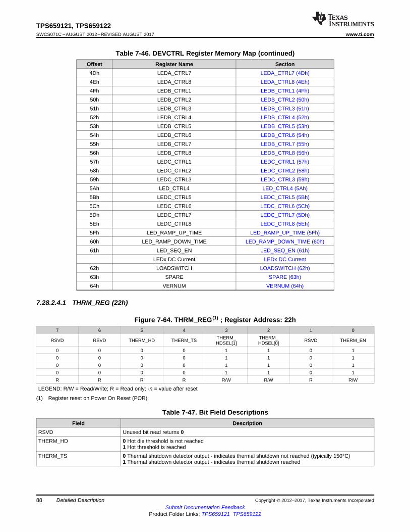
88
TPS659121, TPS659122SWCS071C –AUGUST 2012–REVISED AUGUST 2017 www.ti.com
Submit Documentation FeedbackProduct Folder Links: TPS659121 TPS659122
Detailed Description Copyright © 2012–2017, Texas Instruments Incorporated
Table 7-46. DEVCTRL Register Memory Map (continued)Offset Register Name Section4Dh LEDA_CTRL7 LEDA_CTRL7 (4Dh)4Eh LEDA_CTRL8 LEDA_CTRL8 (4Eh)4Fh LEDB_CTRL1 LEDB_CTRL1 (4Fh)50h LEDB_CTRL2 LEDB_CTRL2 (50h)51h LEDB_CTRL3 LEDB_CTRL3 (51h)52h LEDB_CTRL4 LEDB_CTRL4 (52h)53h LEDB_CTRL5 LEDB_CTRL5 (53h)54h LEDB_CTRL6 LEDB_CTRL6 (54h)55h LEDB_CTRL7 LEDB_CTRL7 (55h)56h LEDB_CTRL8 LEDB_CTRL8 (56h)57h LEDC_CTRL1 LEDC_CTRL1 (57h)58h LEDC_CTRL2 LEDC_CTRL2 (58h)59h LEDC_CTRL3 LEDC_CTRL3 (59h)5Ah LED_CTRL4 LED_CTRL4 (5Ah)5Bh LEDC_CTRL5 LEDC_CTRL5 (5Bh)5Ch LEDC_CTRL6 LEDC_CTRL6 (5Ch)5Dh LEDC_CTRL7 LEDC_CTRL7 (5Dh)5Eh LEDC_CTRL8 LEDC_CTRL8 (5Eh)5Fh LED_RAMP_UP_TIME LED_RAMP_UP_TIME (5Fh)60h LED_RAMP_DOWN_TIME LED_RAMP_DOWN_TIME (60h)61h LED_SEQ_EN LED_SEQ_EN (61h)
LEDx DC Current LEDx DC Current62h LOADSWITCH LOADSWITCH (62h)63h SPARE SPARE (63h)64h VERNUM VERNUM (64h)
7.28.2.4.1 THRM_REG (22h)
(1) Register reset on Power On Reset (POR)
Figure 7-64. THRM_REG (1) ; Register Address: 22h7 6 5 4 3 2 1 0
RSVD RSVD THERM_HD THERM_TS THERM_HDSEL[1]
THERM_HDSEL[0] RSVD THERM_EN
0 0 0 0 1 1 0 10 0 0 0 1 1 0 10 0 0 0 1 1 0 10 0 0 0 1 1 0 1R R R R R/W R/W R R/W
LEGEND: R/W = Read/Write; R = Read only; -n = value after reset
Table 7-47. Bit Field DescriptionsField Description
RSVD Unused bit read returns 0THERM_HD 0 Hot die threshold is not reached
1 Hot threshold is reachedTHERM_TS 0 Thermal shutdown detector output - indicates thermal shutdown not reached (typically 150°C)
1 Thermal shutdown detector output - indicates thermal shutdown reached
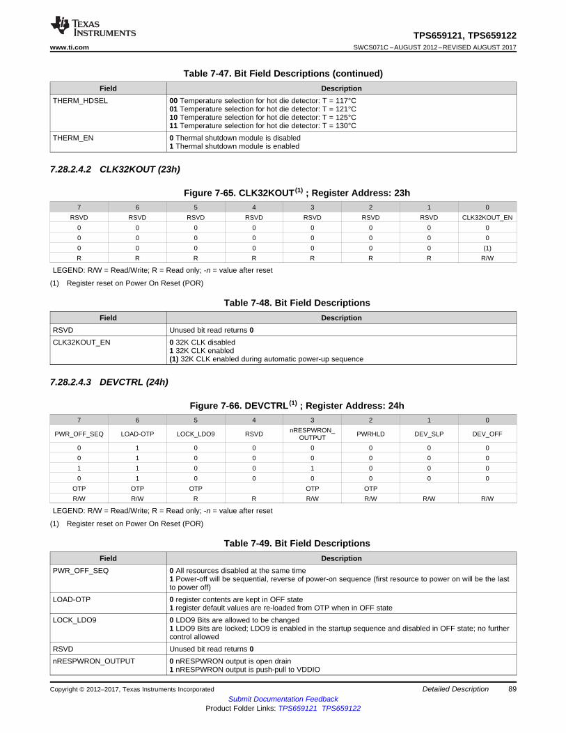
89
TPS659121, TPS659122www.ti.com SWCS071C –AUGUST 2012–REVISED AUGUST 2017
Submit Documentation FeedbackProduct Folder Links: TPS659121 TPS659122
Detailed DescriptionCopyright © 2012–2017, Texas Instruments Incorporated
Table 7-47. Bit Field Descriptions (continued)Field Description
THERM_HDSEL 00 Temperature selection for hot die detector: T = 117°C01 Temperature selection for hot die detector: T = 121°C10 Temperature selection for hot die detector: T = 125°C11 Temperature selection for hot die detector: T = 130°C
THERM_EN 0 Thermal shutdown module is disabled1 Thermal shutdown module is enabled
7.28.2.4.2 CLK32KOUT (23h)
(1) Register reset on Power On Reset (POR)
Figure 7-65. CLK32KOUT (1) ; Register Address: 23h7 6 5 4 3 2 1 0
RSVD RSVD RSVD RSVD RSVD RSVD RSVD CLK32KOUT_EN0 0 0 0 0 0 0 00 0 0 0 0 0 0 00 0 0 0 0 0 0 (1)R R R R R R R R/W
LEGEND: R/W = Read/Write; R = Read only; -n = value after reset
Table 7-48. Bit Field DescriptionsField Description
RSVD Unused bit read returns 0CLK32KOUT_EN 0 32K CLK disabled
1 32K CLK enabled(1) 32K CLK enabled during automatic power-up sequence
7.28.2.4.3 DEVCTRL (24h)
(1) Register reset on Power On Reset (POR)
Figure 7-66. DEVCTRL (1) ; Register Address: 24h7 6 5 4 3 2 1 0
PWR_OFF_SEQ LOAD-OTP LOCK_LDO9 RSVD nRESPWRON_OUTPUT PWRHLD DEV_SLP DEV_OFF
0 1 0 0 0 0 0 00 1 0 0 0 0 0 01 1 0 0 1 0 0 00 1 0 0 0 0 0 0
OTP OTP OTP OTP OTPR/W R/W R R R/W R/W R/W R/W
LEGEND: R/W = Read/Write; R = Read only; -n = value after reset
Table 7-49. Bit Field DescriptionsField Description
PWR_OFF_SEQ 0 All resources disabled at the same time1 Power-off will be sequential, reverse of power-on sequence (first resource to power on will be the lastto power off)
LOAD-OTP 0 register contents are kept in OFF state1 register default values are re-loaded from OTP when in OFF state
LOCK_LDO9 0 LDO9 Bits are allowed to be changed1 LDO9 Bits are locked; LDO9 is enabled in the startup sequence and disabled in OFF state; no furthercontrol allowed
RSVD Unused bit read returns 0nRESPWRON_OUTPUT 0 nRESPWRON output is open drain
1 nRESPWRON output is push-pull to VDDIO
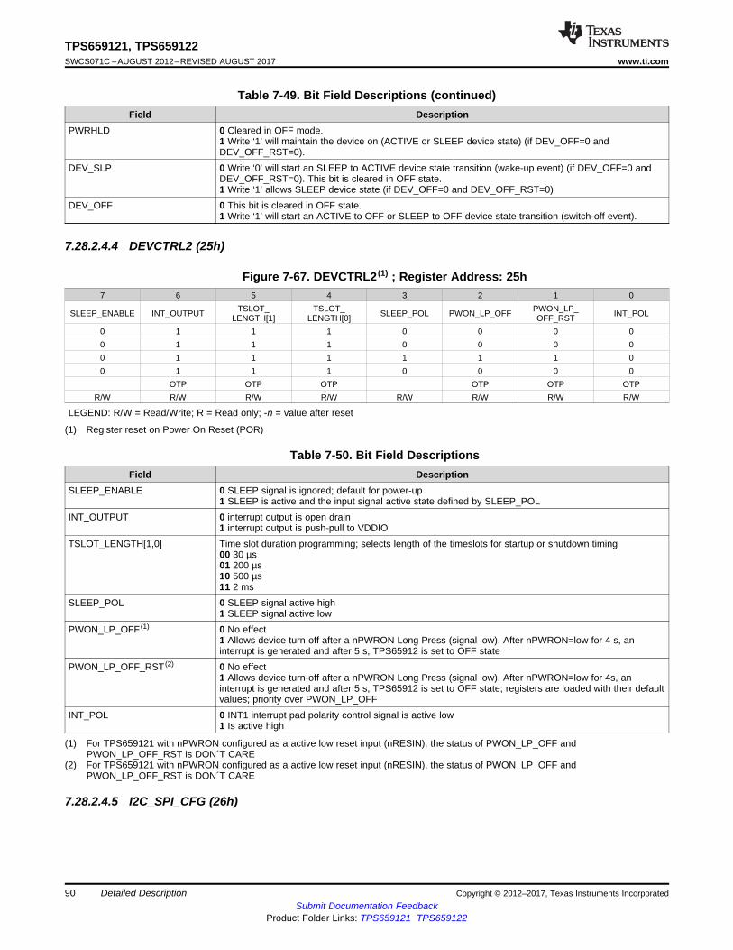
90
TPS659121, TPS659122SWCS071C –AUGUST 2012–REVISED AUGUST 2017 www.ti.com
Submit Documentation FeedbackProduct Folder Links: TPS659121 TPS659122
Detailed Description Copyright © 2012–2017, Texas Instruments Incorporated
Table 7-49. Bit Field Descriptions (continued)Field Description
PWRHLD 0 Cleared in OFF mode.1 Write ‘1’ will maintain the device on (ACTIVE or SLEEP device state) (if DEV_OFF=0 andDEV_OFF_RST=0).
DEV_SLP 0 Write ‘0’ will start an SLEEP to ACTIVE device state transition (wake-up event) (if DEV_OFF=0 andDEV_OFF_RST=0). This bit is cleared in OFF state.1 Write ‘1’ allows SLEEP device state (if DEV_OFF=0 and DEV_OFF_RST=0)
DEV_OFF 0 This bit is cleared in OFF state.1 Write ‘1’ will start an ACTIVE to OFF or SLEEP to OFF device state transition (switch-off event).
7.28.2.4.4 DEVCTRL2 (25h)
(1) Register reset on Power On Reset (POR)
Figure 7-67. DEVCTRL2 (1) ; Register Address: 25h7 6 5 4 3 2 1 0
SLEEP_ENABLE INT_OUTPUT TSLOT_LENGTH[1]
TSLOT_LENGTH[0] SLEEP_POL PWON_LP_OFF PWON_LP_
OFF_RST INT_POL
0 1 1 1 0 0 0 00 1 1 1 0 0 0 00 1 1 1 1 1 1 00 1 1 1 0 0 0 0
OTP OTP OTP OTP OTP OTPR/W R/W R/W R/W R/W R/W R/W R/W
LEGEND: R/W = Read/Write; R = Read only; -n = value after reset
(1) For TPS659121 with nPWRON configured as a active low reset input (nRESIN), the status of PWON_LP_OFF andPWON_LP_OFF_RST is DON´T CARE
(2) For TPS659121 with nPWRON configured as a active low reset input (nRESIN), the status of PWON_LP_OFF andPWON_LP_OFF_RST is DON´T CARE
Table 7-50. Bit Field DescriptionsField Description
SLEEP_ENABLE 0 SLEEP signal is ignored; default for power-up1 SLEEP is active and the input signal active state defined by SLEEP_POL
INT_OUTPUT 0 interrupt output is open drain1 interrupt output is push-pull to VDDIO
TSLOT_LENGTH[1,0] Time slot duration programming; selects length of the timeslots for startup or shutdown timing00 30 µs01 200 µs10 500 µs11 2 ms
SLEEP_POL 0 SLEEP signal active high1 SLEEP signal active low
PWON_LP_OFF (1) 0 No effect1 Allows device turn-off after a nPWRON Long Press (signal low). After nPWRON=low for 4 s, aninterrupt is generated and after 5 s, TPS65912 is set to OFF state
PWON_LP_OFF_RST (2) 0 No effect1 Allows device turn-off after a nPWRON Long Press (signal low). After nPWRON=low for 4s, aninterrupt is generated and after 5 s, TPS65912 is set to OFF state; registers are loaded with their defaultvalues; priority over PWON_LP_OFF
INT_POL 0 INT1 interrupt pad polarity control signal is active low1 Is active high
7.28.2.4.5 I2C_SPI_CFG (26h)
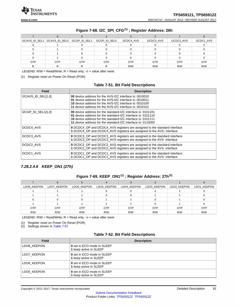
91
TPS659121, TPS659122www.ti.com SWCS071C –AUGUST 2012–REVISED AUGUST 2017
Submit Documentation FeedbackProduct Folder Links: TPS659121 TPS659122
Detailed DescriptionCopyright © 2012–2017, Texas Instruments Incorporated
(1) Register reset on Power On Reset (POR)
Figure 7-68. I2C_SPI_CFG (1) ; Register Address: 26h7 6 5 4 3 2 1 0
I2CAVS_ID_SEL1 I2CAVS_ID_SEL0 I2CGP_ID_SEL1 I2CGP_ID_SEL0 DCDC4_AVS DCDC3_AVS DCDC2_AVS DCDC1_AVS0 1 0 0 0 0 0 00 1 0 0 0 0 0 00 1 0 0 0 0 0 00 1 0 0 0 0 0 0
OTP OTP OTP OTP OTP OTP OTP OTPR R R R R/W R/W R/W R/W
LEGEND: R/W = Read/Write; R = Read only; -n = value after reset
Table 7-51. Bit Field DescriptionsField Description
I2CAVS_ID_SEL[1,0] 00 device address for the AVS-I2C interface is: 001001001 device address for the AVS-I2C interface is: 001001110 device address for the AVS-I2C interface is: 001010011 device address for the AVS-I2C interface is: 0010101
I2CGP_ID_SEL1[1,0] 00 device address for the standard-I2C interface is: 010110101 device address for the standard-I2C interface is: 010111010 device address for the standard-I2C interface is: 010111111 device address for the standard-I2C interface is: 0110000
DCDC4_AVS 0 DCDC4_OP and DCDC4_AVS registers are assigned to the standard interface1 DCDC4_OP and DCDC4_AVS registera are assigned to the AVS- interface
DCDC3_AVS 0 DCDC3_OP and DCDC3_AVS registers are assigned to the standard interface1 DCDC3_OP and DCDC3_AVS registers are assigned to the AVS- interface
DCDC2_AVS 0 DCDC2_OP and DCDC2_AVS registers are assigned to the standard interface1 DCDC2_OP and DCDC2_AVS registers are assigned to the AVS- interface
DCDC1_AVS 0 DCDC1_OP and DCDC1_AVS registers are assigned to the standard interface1 DCDC1_OP and DCDC1_AVS registers are assigned to the AVS- interface
7.28.2.4.6 KEEP_ON1 (27h)
(1) Register reset on Power On Reset (POR)(2) Settings shown in Table 7-57
Figure 7-69. KEEP_ON1 (1) ; Register Address: 27h (2)
7 6 5 4 3 2 1 0LDO8_KEEPON LDO7_KEEPON LDO6_KEEPON LDO5_KEEPON LDO4_KEEPON LDO3_KEEPON LDO2_KEEPON LDO1_KEEPON
1 1 1 0 0 1 1 01 1 1 0 0 1 1 00 0 0 1 1 0 1 01 1 1 1 1 0 1 0
OTP OTP OTP OTP OTP OTP OTP OTPR/W R/W R/W R/W R/W R/W R/W R/W
LEGEND: R/W = Read/Write; R = Read only; -n = value after reset
Table 7-52. Bit Field DescriptionsField Description
LDO8_KEEPON 0 set in ECO mode in SLEEP1 keep active in SLEEP
LDO7_KEEPON 0 set in ECO mode in SLEEP1 keep active in SLEEP
LDO6_KEEPON 0 set in ECO mode in SLEEP1 keep active in SLEEP
LDO5_KEEPON 0 set in ECO mode in SLEEP1 keep active in SLEEP
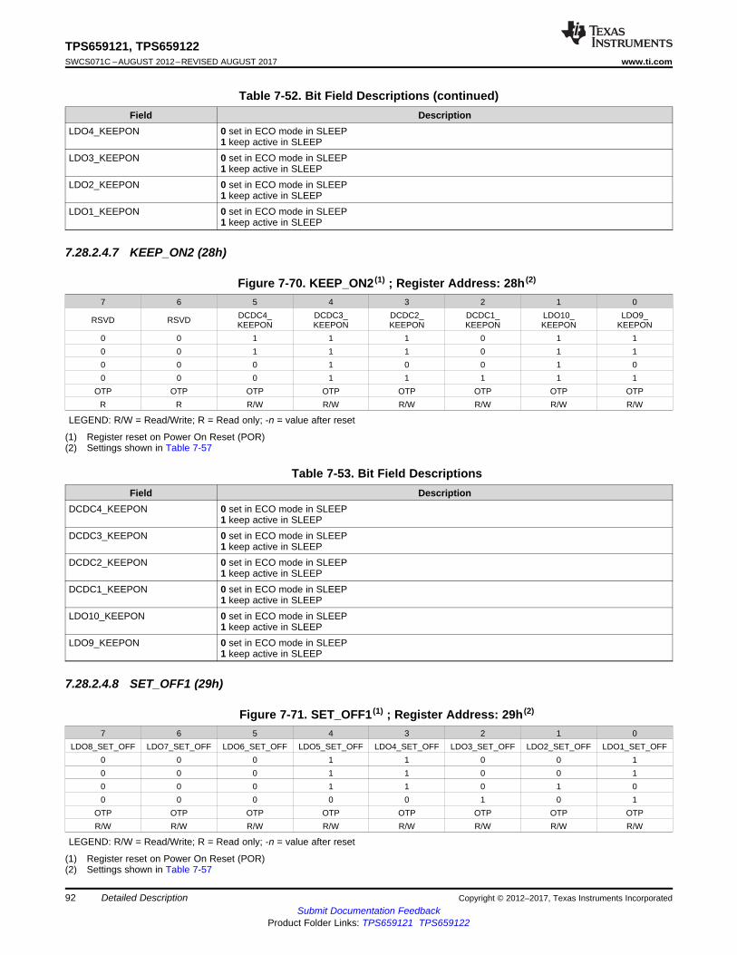
92
TPS659121, TPS659122SWCS071C –AUGUST 2012–REVISED AUGUST 2017 www.ti.com
Submit Documentation FeedbackProduct Folder Links: TPS659121 TPS659122
Detailed Description Copyright © 2012–2017, Texas Instruments Incorporated
Table 7-52. Bit Field Descriptions (continued)Field Description
LDO4_KEEPON 0 set in ECO mode in SLEEP1 keep active in SLEEP
LDO3_KEEPON 0 set in ECO mode in SLEEP1 keep active in SLEEP
LDO2_KEEPON 0 set in ECO mode in SLEEP1 keep active in SLEEP
LDO1_KEEPON 0 set in ECO mode in SLEEP1 keep active in SLEEP
7.28.2.4.7 KEEP_ON2 (28h)
(1) Register reset on Power On Reset (POR)(2) Settings shown in Table 7-57
Figure 7-70. KEEP_ON2 (1) ; Register Address: 28h (2)
7 6 5 4 3 2 1 0
RSVD RSVD DCDC4_KEEPON
DCDC3_KEEPON
DCDC2_KEEPON
DCDC1_KEEPON
LDO10_KEEPON
LDO9_KEEPON
0 0 1 1 1 0 1 10 0 1 1 1 0 1 10 0 0 1 0 0 1 00 0 0 1 1 1 1 1
OTP OTP OTP OTP OTP OTP OTP OTPR R R/W R/W R/W R/W R/W R/W
LEGEND: R/W = Read/Write; R = Read only; -n = value after reset
Table 7-53. Bit Field DescriptionsField Description
DCDC4_KEEPON 0 set in ECO mode in SLEEP1 keep active in SLEEP
DCDC3_KEEPON 0 set in ECO mode in SLEEP1 keep active in SLEEP
DCDC2_KEEPON 0 set in ECO mode in SLEEP1 keep active in SLEEP
DCDC1_KEEPON 0 set in ECO mode in SLEEP1 keep active in SLEEP
LDO10_KEEPON 0 set in ECO mode in SLEEP1 keep active in SLEEP
LDO9_KEEPON 0 set in ECO mode in SLEEP1 keep active in SLEEP
7.28.2.4.8 SET_OFF1 (29h)
(1) Register reset on Power On Reset (POR)(2) Settings shown in Table 7-57
Figure 7-71. SET_OFF1 (1) ; Register Address: 29h (2)
7 6 5 4 3 2 1 0LDO8_SET_OFF LDO7_SET_OFF LDO6_SET_OFF LDO5_SET_OFF LDO4_SET_OFF LDO3_SET_OFF LDO2_SET_OFF LDO1_SET_OFF
0 0 0 1 1 0 0 10 0 0 1 1 0 0 10 0 0 1 1 0 1 00 0 0 0 0 1 0 1
OTP OTP OTP OTP OTP OTP OTP OTPR/W R/W R/W R/W R/W R/W R/W R/W
LEGEND: R/W = Read/Write; R = Read only; -n = value after reset
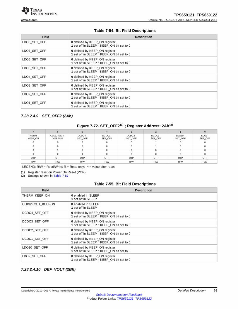
93
TPS659121, TPS659122www.ti.com SWCS071C –AUGUST 2012–REVISED AUGUST 2017
Submit Documentation FeedbackProduct Folder Links: TPS659121 TPS659122
Detailed DescriptionCopyright © 2012–2017, Texas Instruments Incorporated
Table 7-54. Bit Field DescriptionsField Description
LDO8_SET_OFF 0 defined by KEEP_ON register1 set off in SLEEP if KEEP_ON bit set to 0
LDO7_SET_OFF 0 defined by KEEP_ON register1 set off in SLEEP if KEEP_ON bit set to 0
LDO6_SET_OFF 0 defined by KEEP_ON register1 set off in SLEEP if KEEP_ON bit set to 0
LDO5_SET_OFF 0 defined by KEEP_ON register1 set off in SLEEP if KEEP_ON bit set to 0
LDO4_SET_OFF 0 defined by KEEP_ON register1 set off in SLEEP if KEEP_ON bit set to 0
LDO3_SET_OFF 0 defined by KEEP_ON register1 set off in SLEEP if KEEP_ON bit set to 0
LDO2_SET_OFF 0 defined by KEEP_ON register1 set off in SLEEP if KEEP_ON bit set to 0
LDO1_SET_OFF 0 defined by KEEP_ON register1 set off in SLEEP if KEEP_ON bit set to 0
7.28.2.4.9 SET_OFF2 (2Ah)
(1) Register reset on Power On Reset (POR)(2) Settings shown in Table 7-57
Figure 7-72. SET_OFF2 (1) ; Register Address: 2Ah (2)
7 6 5 4 3 2 1 0
THERM_KEEP_ON
CLK32KOUT_KEEPON
DCDC4_SET_OFF
DCDC3_SET_OFF
DCDC2_SET_OFF
DCDC1_SET_OFF
LDO10_SET_OFF
LDO9_SET_OFF
0 0 0 0 0 1 0 0
0 0 0 0 0 1 0 0
0 1 0 0 0 0 0 0
0 0 1 0 0 0 0 0
OTP OTP OTP OTP OTP OTP OTP OTP
R/W R/W R/W R/W R/W R/W R/W R/W
LEGEND: R/W = Read/Write; R = Read only; -n = value after reset
Table 7-55. Bit Field DescriptionsField Description
THERM_KEEP_ON 0 enabled in SLEEP1 set off in SLEEP
CLK32KOUT_KEEPON 0 enabled in SLEEP1 set off in SLEEP
DCDC4_SET_OFF 0 defined by KEEP_ON register1 set off in SLEEP if KEEP_ON bit set to 0
DCDC3_SET_OFF 0 defined by KEEP_ON register1 set off in SLEEP if KEEP_ON bit set to 0
DCDC2_SET_OFF 0 defined by KEEP_ON register1 set off in SLEEP if KEEP_ON bit set to 0
DCDC1_SET_OFF 0 defined by KEEP_ON register1 set off in SLEEP if KEEP_ON bit set to 0
LDO10_SET_OFF 0 defined by KEEP_ON register1 set off in SLEEP if KEEP_ON bit set to 0
LDO9_SET_OFF 0 defined by KEEP_ON register1 set off in SLEEP if KEEP_ON bit set to 0
7.28.2.4.10 DEF_VOLT (2Bh)
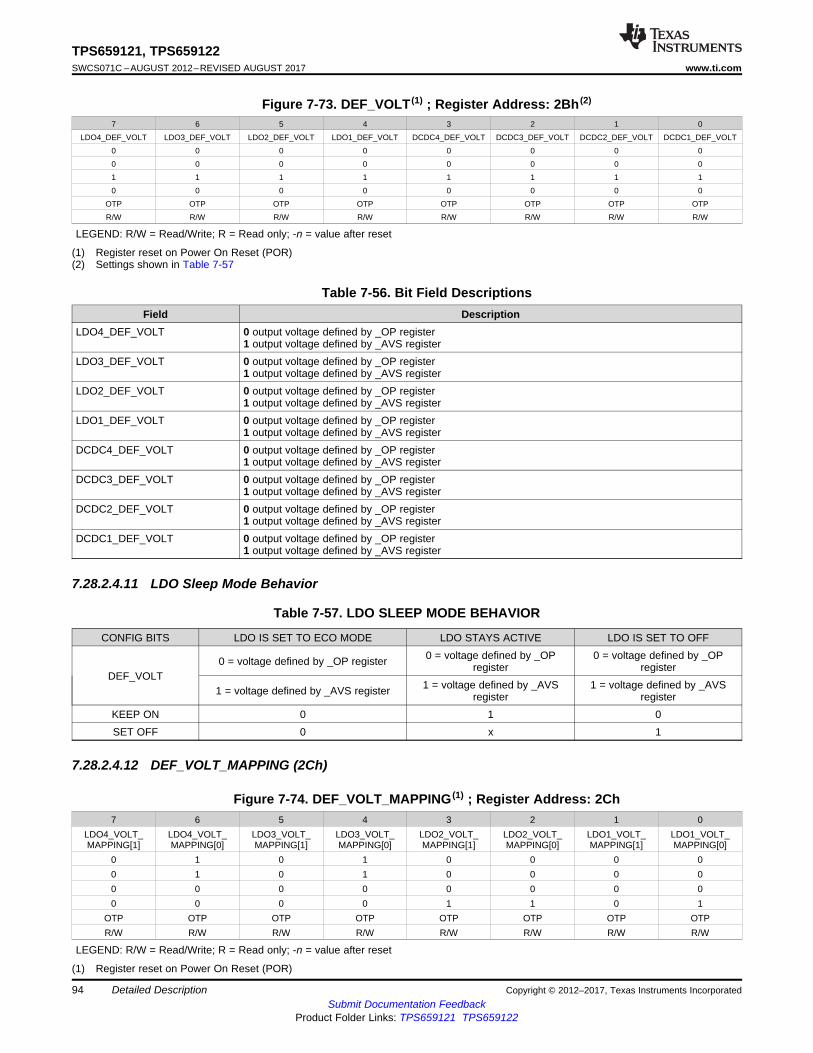
94
TPS659121, TPS659122SWCS071C –AUGUST 2012–REVISED AUGUST 2017 www.ti.com
Submit Documentation FeedbackProduct Folder Links: TPS659121 TPS659122
Detailed Description Copyright © 2012–2017, Texas Instruments Incorporated
(1) Register reset on Power On Reset (POR)(2) Settings shown in Table 7-57
Figure 7-73. DEF_VOLT (1) ; Register Address: 2Bh (2)
7 6 5 4 3 2 1 0
LDO4_DEF_VOLT LDO3_DEF_VOLT LDO2_DEF_VOLT LDO1_DEF_VOLT DCDC4_DEF_VOLT DCDC3_DEF_VOLT DCDC2_DEF_VOLT DCDC1_DEF_VOLT
0 0 0 0 0 0 0 0
0 0 0 0 0 0 0 0
1 1 1 1 1 1 1 1
0 0 0 0 0 0 0 0
OTP OTP OTP OTP OTP OTP OTP OTP
R/W R/W R/W R/W R/W R/W R/W R/W
LEGEND: R/W = Read/Write; R = Read only; -n = value after reset
Table 7-56. Bit Field DescriptionsField Description
LDO4_DEF_VOLT 0 output voltage defined by _OP register1 output voltage defined by _AVS register
LDO3_DEF_VOLT 0 output voltage defined by _OP register1 output voltage defined by _AVS register
LDO2_DEF_VOLT 0 output voltage defined by _OP register1 output voltage defined by _AVS register
LDO1_DEF_VOLT 0 output voltage defined by _OP register1 output voltage defined by _AVS register
DCDC4_DEF_VOLT 0 output voltage defined by _OP register1 output voltage defined by _AVS register
DCDC3_DEF_VOLT 0 output voltage defined by _OP register1 output voltage defined by _AVS register
DCDC2_DEF_VOLT 0 output voltage defined by _OP register1 output voltage defined by _AVS register
DCDC1_DEF_VOLT 0 output voltage defined by _OP register1 output voltage defined by _AVS register
7.28.2.4.11 LDO Sleep Mode Behavior
Table 7-57. LDO SLEEP MODE BEHAVIOR
CONFIG BITS LDO IS SET TO ECO MODE LDO STAYS ACTIVE LDO IS SET TO OFF
DEF_VOLT0 = voltage defined by _OP register 0 = voltage defined by _OP
register0 = voltage defined by _OP
register
1 = voltage defined by _AVS register 1 = voltage defined by _AVSregister
1 = voltage defined by _AVSregister
KEEP ON 0 1 0SET OFF 0 x 1
7.28.2.4.12 DEF_VOLT_MAPPING (2Ch)
(1) Register reset on Power On Reset (POR)
Figure 7-74. DEF_VOLT_MAPPING (1) ; Register Address: 2Ch7 6 5 4 3 2 1 0
LDO4_VOLT_MAPPING[1]
LDO4_VOLT_MAPPING[0]
LDO3_VOLT_MAPPING[1]
LDO3_VOLT_MAPPING[0]
LDO2_VOLT_MAPPING[1]
LDO2_VOLT_MAPPING[0]
LDO1_VOLT_MAPPING[1]
LDO1_VOLT_MAPPING[0]
0 1 0 1 0 0 0 00 1 0 1 0 0 0 00 0 0 0 0 0 0 00 0 0 0 1 1 0 1
OTP OTP OTP OTP OTP OTP OTP OTPR/W R/W R/W R/W R/W R/W R/W R/W
LEGEND: R/W = Read/Write; R = Read only; -n = value after reset
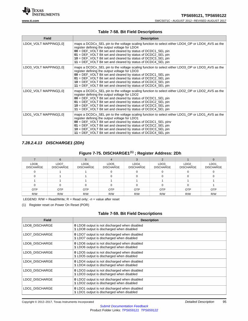
95
TPS659121, TPS659122www.ti.com SWCS071C –AUGUST 2012–REVISED AUGUST 2017
Submit Documentation FeedbackProduct Folder Links: TPS659121 TPS659122
Detailed DescriptionCopyright © 2012–2017, Texas Instruments Incorporated
Table 7-58. Bit Field DescriptionsField Description
LDO4_VOLT MAPPING[1,0] maps a DCDCx_SEL pin to the voltage scaling function to select either LDO4_OP or LDO4_AVS as theregister defining the output voltage for LDO400 = DEF_VOLT Bit set and cleared by status of DCDC1_SEL pin01 = DEF_VOLT Bit set and cleared by status of DCDC2_SEL pin10 = DEF_VOLT Bit set and cleared by status of DCDC3_SEL pin11 = DEF_VOLT Bit set and cleared by status of DCDC4_SEL pin
LDO3_VOLT MAPPING[1,0] maps a DCDCx_SEL pin to the voltage scaling function to select either LDO3_OP or LDO3_AVS as theregister defining the output voltage for LDO300 = DEF_VOLT Bit set and cleared by status of DCDC1_SEL pin01 = DEF_VOLT Bit set and cleared by status of DCDC2_SEL pin10 = DEF_VOLT Bit set and cleared by status of DCDC3_SEL pin11 = DEF_VOLT Bit set and cleared by status of DCDC4_SEL pin
LDO2_VOLT MAPPING[1,0] maps a DCDCx_SEL pin to the voltage scaling function to select either LDO2_OP or LDO2_AVS as theregister defining the output voltage for LDO200 = DEF_VOLT Bit set and cleared by status of DCDC1_SEL pin01 = DEF_VOLT Bit set and cleared by status of DCDC2_SEL pin10 = DEF_VOLT Bit set and cleared by status of DCDC3_SEL pin11 = DEF_VOLT Bit set and cleared by status of DCDC4_SEL pin
LDO1_VOLT MAPPING[1,0] maps a DCDCx_SEL pin to the voltage scaling function to select either LDO1_OP or LDO1_AVS as theregister defining the output voltage for LDO100 = DEF_VOLT Bit set and cleared by status of DCDC1_SEL pinv01 = DEF_VOLT Bit set and cleared by status of DCDC2_SEL pin10 = DEF_VOLT Bit set and cleared by status of DCDC3_SEL pin11 = DEF_VOLT Bit set and cleared by status of DCDC4_SEL pin
7.28.2.4.13 DISCHARGE1 (2Dh)
(1) Register reset on Power On Reset (POR)
Figure 7-75. DISCHARGE1 (1) ; Register Address: 2Dh7 6 5 4 3 2 1 0
LDO8_DISCHARGE
LDO7_DISCHARGE
LDO6_DISCHARGE
LDO5_DISCHARGE
LDO4_DISCHARGE
LDO3_DISCHARGE
LDO2_DISCHARGE
LDO1_DISCHARGE
0 1 1 0 0 0 0 00 1 1 0 0 0 0 01 1 1 1 1 1 1 10 0 0 0 0 0 0 1
OTP OTP OTP OTP OTP OTP OTP OTPR/W R/W R/W R/W R/W R/W R/W R/W
LEGEND: R/W = Read/Write; R = Read only; -n = value after reset
Table 7-59. Bit Field DescriptionsField Description
LDO8_DISCHARGE 0 LDO8 output is not discharged when disabled1 LDO8 output is discharged when disabled
LDO7_DISCHARGE 0 LDO7 output is not discharged when disabled1 LDO7 output is discharged when disabled
LDO6_DISCHARGE 0 LDO6 output is not discharged when disabled1 LDO6 output is discharged when disabled
LDO5_DISCHARGE 0 LDO5 output is not discharged when disabled1 LDO5 output is discharged when disabled
LDO4_DISCHARGE 0 LDO4 output is not discharged when disabled1 LDO4 output is discharged when disabled
LDO3_DISCHARGE 0 LDO3 output is not discharged when disabled1 LDO3 output is discharged when disabled
LDO2_DISCHARGE 0 LDO2 output is not discharged when disabled1 LDO2 output is discharged when disabled
LDO1_DISCHARGE 0 LDO1 output is not discharged when disabled1 LDO1 output is discharged when disabled
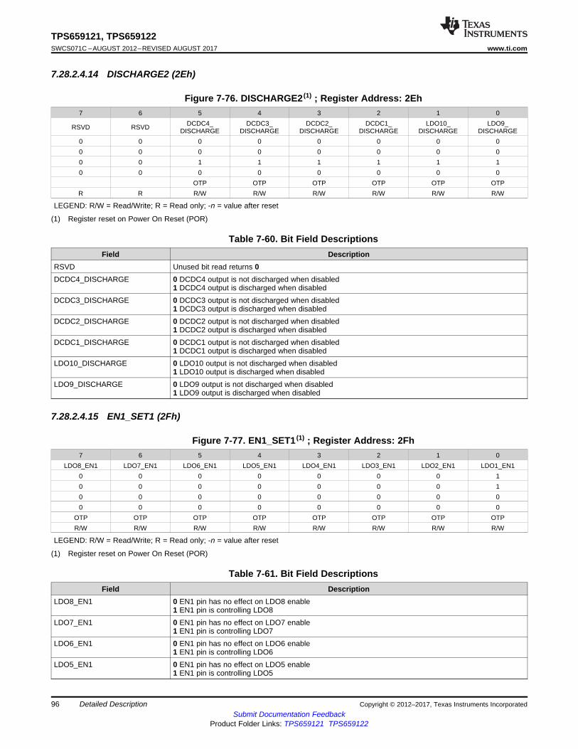
96
TPS659121, TPS659122SWCS071C –AUGUST 2012–REVISED AUGUST 2017 www.ti.com
Submit Documentation FeedbackProduct Folder Links: TPS659121 TPS659122
Detailed Description Copyright © 2012–2017, Texas Instruments Incorporated
7.28.2.4.14 DISCHARGE2 (2Eh)
(1) Register reset on Power On Reset (POR)
Figure 7-76. DISCHARGE2 (1) ; Register Address: 2Eh7 6 5 4 3 2 1 0
RSVD RSVD DCDC4_DISCHARGE
DCDC3_DISCHARGE
DCDC2_DISCHARGE
DCDC1_DISCHARGE
LDO10_DISCHARGE
LDO9_DISCHARGE
0 0 0 0 0 0 0 00 0 0 0 0 0 0 00 0 1 1 1 1 1 10 0 0 0 0 0 0 0
OTP OTP OTP OTP OTP OTPR R R/W R/W R/W R/W R/W R/W
LEGEND: R/W = Read/Write; R = Read only; -n = value after reset
Table 7-60. Bit Field DescriptionsField Description
RSVD Unused bit read returns 0DCDC4_DISCHARGE 0 DCDC4 output is not discharged when disabled
1 DCDC4 output is discharged when disabledDCDC3_DISCHARGE 0 DCDC3 output is not discharged when disabled
1 DCDC3 output is discharged when disabledDCDC2_DISCHARGE 0 DCDC2 output is not discharged when disabled
1 DCDC2 output is discharged when disabledDCDC1_DISCHARGE 0 DCDC1 output is not discharged when disabled
1 DCDC1 output is discharged when disabledLDO10_DISCHARGE 0 LDO10 output is not discharged when disabled
1 LDO10 output is discharged when disabledLDO9_DISCHARGE 0 LDO9 output is not discharged when disabled
1 LDO9 output is discharged when disabled
7.28.2.4.15 EN1_SET1 (2Fh)
(1) Register reset on Power On Reset (POR)
Figure 7-77. EN1_SET1 (1) ; Register Address: 2Fh7 6 5 4 3 2 1 0
LDO8_EN1 LDO7_EN1 LDO6_EN1 LDO5_EN1 LDO4_EN1 LDO3_EN1 LDO2_EN1 LDO1_EN10 0 0 0 0 0 0 10 0 0 0 0 0 0 10 0 0 0 0 0 0 00 0 0 0 0 0 0 0
OTP OTP OTP OTP OTP OTP OTP OTPR/W R/W R/W R/W R/W R/W R/W R/W
LEGEND: R/W = Read/Write; R = Read only; -n = value after reset
Table 7-61. Bit Field DescriptionsField Description
LDO8_EN1 0 EN1 pin has no effect on LDO8 enable1 EN1 pin is controlling LDO8
LDO7_EN1 0 EN1 pin has no effect on LDO7 enable1 EN1 pin is controlling LDO7
LDO6_EN1 0 EN1 pin has no effect on LDO6 enable1 EN1 pin is controlling LDO6
LDO5_EN1 0 EN1 pin has no effect on LDO5 enable1 EN1 pin is controlling LDO5
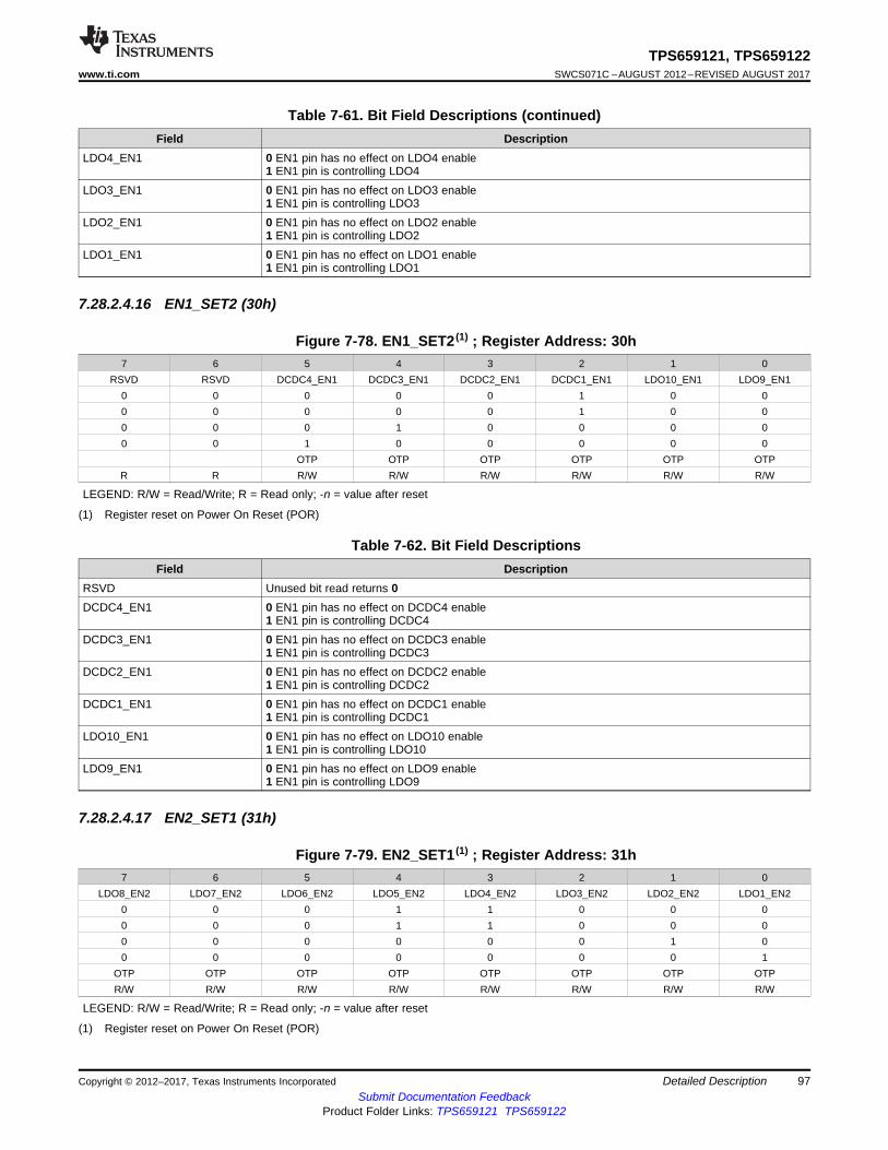
97
TPS659121, TPS659122www.ti.com SWCS071C –AUGUST 2012–REVISED AUGUST 2017
Submit Documentation FeedbackProduct Folder Links: TPS659121 TPS659122
Detailed DescriptionCopyright © 2012–2017, Texas Instruments Incorporated
Table 7-61. Bit Field Descriptions (continued)Field Description
LDO4_EN1 0 EN1 pin has no effect on LDO4 enable1 EN1 pin is controlling LDO4
LDO3_EN1 0 EN1 pin has no effect on LDO3 enable1 EN1 pin is controlling LDO3
LDO2_EN1 0 EN1 pin has no effect on LDO2 enable1 EN1 pin is controlling LDO2
LDO1_EN1 0 EN1 pin has no effect on LDO1 enable1 EN1 pin is controlling LDO1
7.28.2.4.16 EN1_SET2 (30h)
(1) Register reset on Power On Reset (POR)
Figure 7-78. EN1_SET2 (1) ; Register Address: 30h7 6 5 4 3 2 1 0
RSVD RSVD DCDC4_EN1 DCDC3_EN1 DCDC2_EN1 DCDC1_EN1 LDO10_EN1 LDO9_EN10 0 0 0 0 1 0 00 0 0 0 0 1 0 00 0 0 1 0 0 0 00 0 1 0 0 0 0 0
OTP OTP OTP OTP OTP OTPR R R/W R/W R/W R/W R/W R/W
LEGEND: R/W = Read/Write; R = Read only; -n = value after reset
Table 7-62. Bit Field DescriptionsField Description
RSVD Unused bit read returns 0DCDC4_EN1 0 EN1 pin has no effect on DCDC4 enable
1 EN1 pin is controlling DCDC4DCDC3_EN1 0 EN1 pin has no effect on DCDC3 enable
1 EN1 pin is controlling DCDC3DCDC2_EN1 0 EN1 pin has no effect on DCDC2 enable
1 EN1 pin is controlling DCDC2DCDC1_EN1 0 EN1 pin has no effect on DCDC1 enable
1 EN1 pin is controlling DCDC1LDO10_EN1 0 EN1 pin has no effect on LDO10 enable
1 EN1 pin is controlling LDO10LDO9_EN1 0 EN1 pin has no effect on LDO9 enable
1 EN1 pin is controlling LDO9
7.28.2.4.17 EN2_SET1 (31h)
(1) Register reset on Power On Reset (POR)
Figure 7-79. EN2_SET1 (1) ; Register Address: 31h7 6 5 4 3 2 1 0
LDO8_EN2 LDO7_EN2 LDO6_EN2 LDO5_EN2 LDO4_EN2 LDO3_EN2 LDO2_EN2 LDO1_EN20 0 0 1 1 0 0 00 0 0 1 1 0 0 00 0 0 0 0 0 1 00 0 0 0 0 0 0 1
OTP OTP OTP OTP OTP OTP OTP OTPR/W R/W R/W R/W R/W R/W R/W R/W
LEGEND: R/W = Read/Write; R = Read only; -n = value after reset
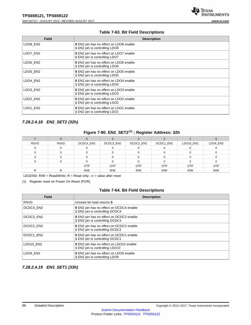
98
TPS659121, TPS659122SWCS071C –AUGUST 2012–REVISED AUGUST 2017 www.ti.com
Submit Documentation FeedbackProduct Folder Links: TPS659121 TPS659122
Detailed Description Copyright © 2012–2017, Texas Instruments Incorporated
Table 7-63. Bit Field DescriptionsField Description
LDO8_EN2 0 EN2 pin has no effect on LDO8 enable1 EN2 pin is controlling LDO8
LDO7_EN2 0 EN2 pin has no effect on LDO7 enable1 EN2 pin is controlling LDO7
LDO6_EN2 0 EN2 pin has no effect on LDO6 enable1 EN2 pin is controlling LDO6
LDO5_EN2 0 EN2 pin has no effect on LDO5 enable1 EN2 pin is controlling LDO5
LDO4_EN2 0 EN2 pin has no effect on LDO4 enable1 EN2 pin is controlling LDO4
LDO3_EN2 0 EN2 pin has no effect on LDO3 enable1 EN2 pin is controlling LDO3
LDO2_EN2 0 EN2 pin has no effect on LDO2 enable1 EN2 pin is controlling LDO2
LDO1_EN2 0 EN2 pin has no effect on LDO1 enable1 EN2 pin is controlling LDO1
7.28.2.4.18 EN2_SET2 (32h)
(1) Register reset on Power On Reset (POR)
Figure 7-80. EN2_SET2 (1) ; Register Address: 32h7 6 5 4 3 2 1 0
RSVD RSVD DCDC4_EN2 DCDC3_EN2 DCDC2_EN2 DCDC1_EN2 LDO10_EN2 LDO9_EN20 0 0 0 0 0 0 00 0 0 0 0 0 0 00 0 0 0 0 0 0 00 0 0 0 0 0 0 0
OTP OTP OTP OTP OTP OTPR R R/W R/W R/W R/W R/W R/W
LEGEND: R/W = Read/Write; R = Read only; -n = value after reset
Table 7-64. Bit Field DescriptionsField Description
RSVD Unused bit read returns 0DCDC4_EN2 0 EN2 pin has no effect on DCDC4 enable
1 EN2 pin is controlling DCDC4DCDC3_EN2 0 EN2 pin has no effect on DCDC3 enable
1 EN2 pin is controlling DCDC3DCDC2_EN2 0 EN2 pin has no effect on DCDC2 enable
1 EN2 pin is controlling DCDC2DCDC1_EN2 0 EN2 pin has no effect on DCDC1 enable
1 EN2 pin is controlling DCDC1LDO10_EN2 0 EN2 pin has no effect on LDO10 enable
1 EN2 pin is controlling LDO10LDO9_EN2 0 EN2 pin has no effect on LDO9 enable
1 EN2 pin is controlling LDO9
7.28.2.4.19 EN3_SET1 (33h)
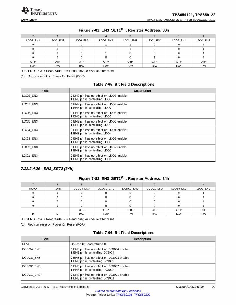
99
TPS659121, TPS659122www.ti.com SWCS071C –AUGUST 2012–REVISED AUGUST 2017
Submit Documentation FeedbackProduct Folder Links: TPS659121 TPS659122
Detailed DescriptionCopyright © 2012–2017, Texas Instruments Incorporated
(1) Register reset on Power On Reset (POR)
Figure 7-81. EN3_SET1 (1) ; Register Address: 33h7 6 5 4 3 2 1 0
LDO8_EN3 LDO7_EN3 LDO6_EN3 LDO5_EN3 LDO4_EN3 LDO3_EN3 LDO2_EN3 LDO1_EN30 0 0 1 1 0 0 00 0 0 1 1 0 0 00 0 0 1 0 0 0 00 0 0 0 0 1 0 0
OTP OTP OTP OTP OTP OTP OTP OTPR/W R/W R/W R/W R/W R/W R/W R/W
LEGEND: R/W = Read/Write; R = Read only; -n = value after reset
Table 7-65. Bit Field DescriptionsField Description
LDO8_EN3 0 EN3 pin has no effect on LDO8 enable1 EN3 pin is controlling LDO8
LDO7_EN3 0 EN3 pin has no effect on LDO7 enable1 EN3 pin is controlling LDO7
LDO6_EN3 0 EN3 pin has no effect on LDO6 enable1 EN3 pin is controlling LDO6
LDO5_EN3 0 EN3 pin has no effect on LDO5 enable1 EN3 pin is controlling LDO5
LDO4_EN3 0 EN3 pin has no effect on LDO4 enable1 EN3 pin is controlling LDO4
LDO3_EN3 0 EN3 pin has no effect on LDO3 enable1 EN3 pin is controlling LDO3
LDO2_EN3 0 EN3 pin has no effect on LDO2 enable1 EN3 pin is controlling LDO2
LDO1_EN3 0 EN3 pin has no effect on LDO1 enable1 EN3 pin is controlling LDO1
7.28.2.4.20 EN3_SET2 (34h)
(1) Register reset on Power On Reset (POR)
Figure 7-82. EN3_SET2 (1) ; Register Address: 34h7 6 5 4 3 2 1 0
RSVD RSVD DCDC4_EN3 DCDC3_EN3 DCDC2_EN3 DCDC1_EN3 LDO10_EN3 LDO9_EN30 0 0 0 0 0 0 00 0 0 0 0 0 0 00 0 0 0 0 0 0 00 0 0 0 0 0 0 0
OTP OTP OTP OTP OTP OTPR R R/W R/W R/W R/W R/W R/W
LEGEND: R/W = Read/Write; R = Read only; -n = value after reset
Table 7-66. Bit Field DescriptionsField Description
RSVD Unused bit read returns 0DCDC4_EN3 0 EN3 pin has no effect on DCDC4 enable
1 EN3 pin is controlling DCDC4DCDC3_EN3 0 EN3 pin has no effect on DCDC3 enable
1 EN3 pin is controlling DCDC3DCDC2_EN3 0 EN3 pin has no effect on DCDC2 enable
1 EN3 pin is controlling DCDC2DCDC1_EN3 0 EN3 pin has no effect on DCDC1 enable
1 EN3 pin is controlling DCDC1
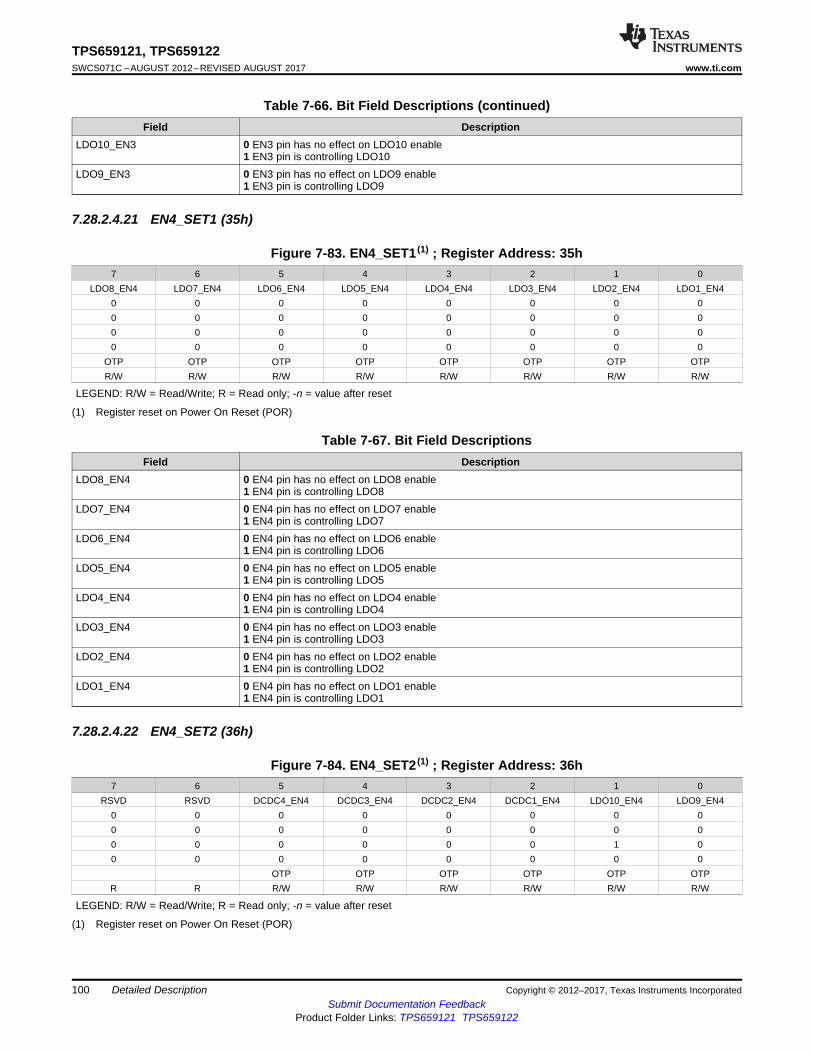
100
TPS659121, TPS659122SWCS071C –AUGUST 2012–REVISED AUGUST 2017 www.ti.com
Submit Documentation FeedbackProduct Folder Links: TPS659121 TPS659122
Detailed Description Copyright © 2012–2017, Texas Instruments Incorporated
Table 7-66. Bit Field Descriptions (continued)Field Description
LDO10_EN3 0 EN3 pin has no effect on LDO10 enable1 EN3 pin is controlling LDO10
LDO9_EN3 0 EN3 pin has no effect on LDO9 enable1 EN3 pin is controlling LDO9
7.28.2.4.21 EN4_SET1 (35h)
(1) Register reset on Power On Reset (POR)
Figure 7-83. EN4_SET1 (1) ; Register Address: 35h7 6 5 4 3 2 1 0
LDO8_EN4 LDO7_EN4 LDO6_EN4 LDO5_EN4 LDO4_EN4 LDO3_EN4 LDO2_EN4 LDO1_EN40 0 0 0 0 0 0 00 0 0 0 0 0 0 00 0 0 0 0 0 0 00 0 0 0 0 0 0 0
OTP OTP OTP OTP OTP OTP OTP OTPR/W R/W R/W R/W R/W R/W R/W R/W
LEGEND: R/W = Read/Write; R = Read only; -n = value after reset
Table 7-67. Bit Field DescriptionsField Description
LDO8_EN4 0 EN4 pin has no effect on LDO8 enable1 EN4 pin is controlling LDO8
LDO7_EN4 0 EN4 pin has no effect on LDO7 enable1 EN4 pin is controlling LDO7
LDO6_EN4 0 EN4 pin has no effect on LDO6 enable1 EN4 pin is controlling LDO6
LDO5_EN4 0 EN4 pin has no effect on LDO5 enable1 EN4 pin is controlling LDO5
LDO4_EN4 0 EN4 pin has no effect on LDO4 enable1 EN4 pin is controlling LDO4
LDO3_EN4 0 EN4 pin has no effect on LDO3 enable1 EN4 pin is controlling LDO3
LDO2_EN4 0 EN4 pin has no effect on LDO2 enable1 EN4 pin is controlling LDO2
LDO1_EN4 0 EN4 pin has no effect on LDO1 enable1 EN4 pin is controlling LDO1
7.28.2.4.22 EN4_SET2 (36h)
(1) Register reset on Power On Reset (POR)
Figure 7-84. EN4_SET2 (1) ; Register Address: 36h7 6 5 4 3 2 1 0
RSVD RSVD DCDC4_EN4 DCDC3_EN4 DCDC2_EN4 DCDC1_EN4 LDO10_EN4 LDO9_EN40 0 0 0 0 0 0 00 0 0 0 0 0 0 00 0 0 0 0 0 1 00 0 0 0 0 0 0 0
OTP OTP OTP OTP OTP OTPR R R/W R/W R/W R/W R/W R/W
LEGEND: R/W = Read/Write; R = Read only; -n = value after reset
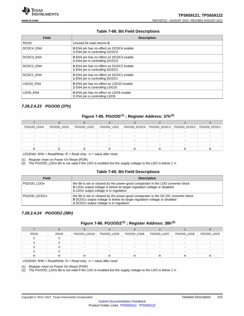
101
TPS659121, TPS659122www.ti.com SWCS071C –AUGUST 2012–REVISED AUGUST 2017
Submit Documentation FeedbackProduct Folder Links: TPS659121 TPS659122
Detailed DescriptionCopyright © 2012–2017, Texas Instruments Incorporated
Table 7-68. Bit Field DescriptionsField Description
RSVD Unused bit read returns 0DCDC4_EN4 0 EN4 pin has no effect on DCDC4 enable
1 EN4 pin is controlling DCDC4DCDC3_EN4 0 EN4 pin has no effect on DCDC3 enable
1 EN4 pin is controlling DCDC3DCDC2_EN4 0 EN4 pin has no effect on DCDC2 enable
1 EN4 pin is controlling DCDC2DCDC1_EN4 0 EN4 pin has no effect on DCDC1 enable
1 EN4 pin is controlling DCDC1LDO10_EN4 0 EN4 pin has no effect on LDO10 enable
1 EN4 pin is controlling LDO10LDO9_EN4 0 EN4 pin has no effect on LDO9 enable
1 EN4 pin is controlling LDO9
7.28.2.4.23 PGOOD (37h)
(1) Register reset on Power On Reset (POR)(2) The PGOOD_LDOx Bit is not valid if the LDO is enabled but the supply voltage to the LDO is below 1 V.
Figure 7-85. PGOOD (1) ; Register Address: 37h (2)
7 6 5 4 3 2 1 0PGOOD_LDO4 PGOOD_LDO3 PGOOD_LDO2 PGOOD_LDO1 PGOOD_DCDC4 PGOOD_DCDC3 PGOOD_DCDC2 PGOOD_DCDC1
- - - - - - - -- - - - - - - -- - - - - - - -- - - - - - - -R R R R R R R R
LEGEND: R/W = Read/Write; R = Read only; -n = value after reset
Table 7-69. Bit Field DescriptionsField Description
PGOOD_LDOx the Bit is set or cleared by the power-good comparator in the LDO converter block0 LDOx output voltage is below its target regulation voltage or disabled1 LDOx output voltage is in regulation
PGOOD_DCDCx the Bit is set or cleared by the power-good comparator in the DC-DC converter block0 DCDCx output voltage is below its target regulation voltage or disabled1 DCDCx output voltage is in regulation
7.28.2.4.24 PGOOD2 (38h)
(1) Register reset on Power On Reset (POR)(2) The PGOOD_LDOx Bit is not valid if the LDO is enabled but the supply voltage to the LDO is below 1 V.
Figure 7-86. PGOOD2 (1) ; Register Address: 38h (2)
7 6 5 4 3 2 1 0RSVD RSVD PGOOD_LDO10 PGOOD_LDO9 PGOOD_LDO8 PGOOD_LDO7 PGOOD_LDO6 PGOOD_LDO5
0 0 - - - - - -0 0 - - - - - -0 0 - - - - - -0 0 - - - - - -R R R R R R R R
LEGEND: R/W = Read/Write; R = Read only; -n = value after reset
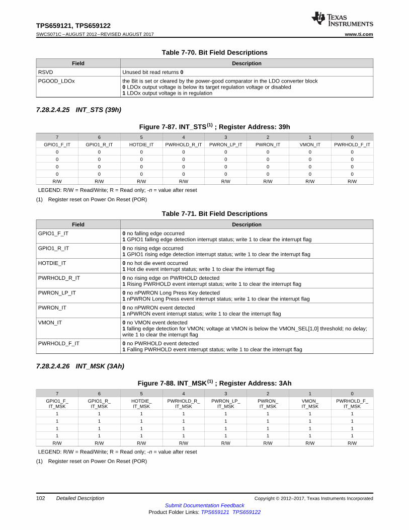
102
TPS659121, TPS659122SWCS071C –AUGUST 2012–REVISED AUGUST 2017 www.ti.com
Submit Documentation FeedbackProduct Folder Links: TPS659121 TPS659122
Detailed Description Copyright © 2012–2017, Texas Instruments Incorporated
Table 7-70. Bit Field DescriptionsField Description
RSVD Unused bit read returns 0PGOOD_LDOx the Bit is set or cleared by the power-good comparator in the LDO converter block
0 LDOx output voltage is below its target regulation voltage or disabled1 LDOx output voltage is in regulation
7.28.2.4.25 INT_STS (39h)
(1) Register reset on Power On Reset (POR)
Figure 7-87. INT_STS (1) ; Register Address: 39h7 6 5 4 3 2 1 0
GPIO1_F_IT GPIO1_R_IT HOTDIE_IT PWRHOLD_R_IT PWRON_LP_IT PWRON_IT VMON_IT PWRHOLD_F_IT0 0 0 0 0 0 0 00 0 0 0 0 0 0 00 0 0 0 0 0 0 00 0 0 0 0 0 0 0
R/W R/W R/W R/W R/W R/W R/W R/W
LEGEND: R/W = Read/Write; R = Read only; -n = value after reset
Table 7-71. Bit Field DescriptionsField Description
GPIO1_F_IT 0 no falling edge occurred1 GPIO1 falling edge detection interrupt status; write 1 to clear the interrupt flag
GPIO1_R_IT 0 no rising edge occurred1 GPIO1 rising edge detection interrupt status; write 1 to clear the interrupt flag
HOTDIE_IT 0 no hot die event occurred1 Hot die event interrupt status; write 1 to clear the interrupt flag
PWRHOLD_R_IT 0 no rising edge on PWRHOLD detected1 Rising PWRHOLD event interrupt status; write 1 to clear the interrupt flag
PWRON_LP_IT 0 no nPWRON Long Press Key detected1 nPWRON Long Press event interrupt status; write 1 to clear the interrupt flag
PWRON_IT 0 no nPWRON event detected1 nPWRON event interrupt status; write 1 to clear the interrupt flag
VMON_IT 0 no VMON event detected1 falling edge detection for VMON; voltage at VMON is below the VMON_SEL[1,0] threshold; no delay;write 1 to clear the interrupt flag
PWRHOLD_F_IT 0 no PWRHOLD event detected1 Falling PWRHOLD event interrupt status; write 1 to clear the interrupt flag
7.28.2.4.26 INT_MSK (3Ah)
(1) Register reset on Power On Reset (POR)
Figure 7-88. INT_MSK (1) ; Register Address: 3Ah7 6 5 4 3 2 1 0
GPIO1_F_IT_MSK
GPIO1_R_IT_MSK
HOTDIE_IT_MSK
PWRHOLD_R_IT_MSK
PWRON_LP_IT_MSK
PWRON_IT_MSK
VMON_IT_MSK
PWRHOLD_F_IT_MSK
1 1 1 1 1 1 1 11 1 1 1 1 1 1 11 1 1 1 1 1 1 11 1 1 1 1 1 1 1
R/W R/W R/W R/W R/W R/W R/W R/W
LEGEND: R/W = Read/Write; R = Read only; -n = value after reset
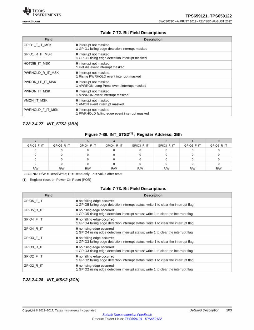
103
TPS659121, TPS659122www.ti.com SWCS071C –AUGUST 2012–REVISED AUGUST 2017
Submit Documentation FeedbackProduct Folder Links: TPS659121 TPS659122
Detailed DescriptionCopyright © 2012–2017, Texas Instruments Incorporated
Table 7-72. Bit Field DescriptionsField Description
GPIO1_F_IT_MSK 0 interrupt not masked1 GPIO1 falling edge detection interrupt masked
GPIO1_R_IT_MSK 0 interrupt not masked1 GPIO1 rising edge detection interrupt masked
HOTDIE_IT_MSK 0 interrupt not masked1 Hot die event interrupt masked
PWRHOLD_R_IT_MSK 0 interrupt not masked1 Rising PWRHOLD event interrupt masked
PWRON_LP_IT_MSK 0 interrupt not masked1 nPWRON Long Press event interrupt masked
PWRON_IT_MSK 0 interrupt not masked1 nPWRON event interrupt masked
VMON_IT_MSK 0 interrupt not masked1 VMON event interrupt masked.
PWRHOLD_F_IT_MSK 0 interrupt not masked1 PWRHOLD falling edge event interrupt masked
7.28.2.4.27 INT_STS2 (3Bh)
(1) Register reset on Power On Reset (POR)
Figure 7-89. INT_STS2 (1) ; Register Address: 3Bh7 6 5 4 3 2 1 0
GPIO5_F_IT GPIO5_R_IT GPIO4_F_IT GPIO4_R_IT GPIO3_F_IT GPIO3_R_IT GPIO2_F_IT GPIO2_R_IT0 0 0 0 0 0 0 00 0 0 0 0 0 0 00 0 0 0 0 0 0 00 0 0 0 0 0 0 0
R/W R/W R/W R/W R/W R/W R/W R/W
LEGEND: R/W = Read/Write; R = Read only; -n = value after reset
Table 7-73. Bit Field DescriptionsField Description
GPIO5_F_IT 0 no falling edge occurred1 GPIO5 falling edge detection interrupt status; write 1 to clear the interrupt flag
GPIO5_R_IT 0 no rising edge occurred1 GPIO5 rising edge detection interrupt status; write 1 to clear the interrupt flag
GPIO4_F_IT 0 no falling edge occurred1 GPIO4 falling edge detection interrupt status; write 1 to clear the interrupt flag
GPIO4_R_IT 0 no rising edge occurred1 GPIO4 rising edge detection interrupt status; write 1 to clear the interrupt flag
GPIO3_F_IT 0 no falling edge occurred1 GPIO3 falling edge detection interrupt status; write 1 to clear the interrupt flag
GPIO3_R_IT 0 no rising edge occurred1 GPIO3 rising edge detection interrupt status; write 1 to clear the interrupt flag
GPIO2_F_IT 0 no falling edge occurred1 GPIO2 falling edge detection interrupt status; write 1 to clear the interrupt flag
GPIO2_R_IT 0 no rising edge occurred1 GPIO2 rising edge detection interrupt status; write 1 to clear the interrupt flag
7.28.2.4.28 INT_MSK2 (3Ch)
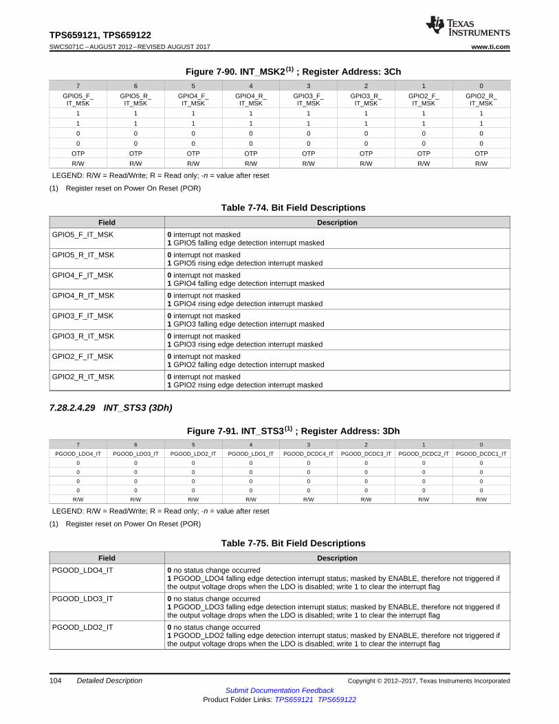
104
TPS659121, TPS659122SWCS071C –AUGUST 2012–REVISED AUGUST 2017 www.ti.com
Submit Documentation FeedbackProduct Folder Links: TPS659121 TPS659122
Detailed Description Copyright © 2012–2017, Texas Instruments Incorporated
(1) Register reset on Power On Reset (POR)
Figure 7-90. INT_MSK2 (1) ; Register Address: 3Ch7 6 5 4 3 2 1 0
GPIO5_F_IT_MSK
GPIO5_R_IT_MSK
GPIO4_F_IT_MSK
GPIO4_R_IT_MSK
GPIO3_F_IT_MSK
GPIO3_R_IT_MSK
GPIO2_F_IT_MSK
GPIO2_R_IT_MSK
1 1 1 1 1 1 1 11 1 1 1 1 1 1 10 0 0 0 0 0 0 00 0 0 0 0 0 0 0
OTP OTP OTP OTP OTP OTP OTP OTPR/W R/W R/W R/W R/W R/W R/W R/W
LEGEND: R/W = Read/Write; R = Read only; -n = value after reset
Table 7-74. Bit Field DescriptionsField Description
GPIO5_F_IT_MSK 0 interrupt not masked1 GPIO5 falling edge detection interrupt masked
GPIO5_R_IT_MSK 0 interrupt not masked1 GPIO5 rising edge detection interrupt masked
GPIO4_F_IT_MSK 0 interrupt not masked1 GPIO4 falling edge detection interrupt masked
GPIO4_R_IT_MSK 0 interrupt not masked1 GPIO4 rising edge detection interrupt masked
GPIO3_F_IT_MSK 0 interrupt not masked1 GPIO3 falling edge detection interrupt masked
GPIO3_R_IT_MSK 0 interrupt not masked1 GPIO3 rising edge detection interrupt masked
GPIO2_F_IT_MSK 0 interrupt not masked1 GPIO2 falling edge detection interrupt masked
GPIO2_R_IT_MSK 0 interrupt not masked1 GPIO2 rising edge detection interrupt masked
7.28.2.4.29 INT_STS3 (3Dh)
(1) Register reset on Power On Reset (POR)
Figure 7-91. INT_STS3 (1) ; Register Address: 3Dh7 6 5 4 3 2 1 0
PGOOD_LDO4_IT PGOOD_LDO3_IT PGOOD_LDO2_IT PGOOD_LDO1_IT PGOOD_DCDC4_IT PGOOD_DCDC3_IT PGOOD_DCDC2_IT PGOOD_DCDC1_IT
0 0 0 0 0 0 0 0
0 0 0 0 0 0 0 0
0 0 0 0 0 0 0 0
0 0 0 0 0 0 0 0
R/W R/W R/W R/W R/W R/W R/W R/W
LEGEND: R/W = Read/Write; R = Read only; -n = value after reset
Table 7-75. Bit Field DescriptionsField Description
PGOOD_LDO4_IT 0 no status change occurred1 PGOOD_LDO4 falling edge detection interrupt status; masked by ENABLE, therefore not triggered ifthe output voltage drops when the LDO is disabled; write 1 to clear the interrupt flag
PGOOD_LDO3_IT 0 no status change occurred1 PGOOD_LDO3 falling edge detection interrupt status; masked by ENABLE, therefore not triggered ifthe output voltage drops when the LDO is disabled; write 1 to clear the interrupt flag
PGOOD_LDO2_IT 0 no status change occurred1 PGOOD_LDO2 falling edge detection interrupt status; masked by ENABLE, therefore not triggered ifthe output voltage drops when the LDO is disabled; write 1 to clear the interrupt flag
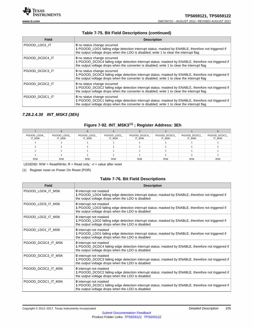
105
TPS659121, TPS659122www.ti.com SWCS071C –AUGUST 2012–REVISED AUGUST 2017
Submit Documentation FeedbackProduct Folder Links: TPS659121 TPS659122
Detailed DescriptionCopyright © 2012–2017, Texas Instruments Incorporated
Table 7-75. Bit Field Descriptions (continued)Field Description
PGOOD_LDO1_IT 0 no status change occurred1 PGOOD_LDO1 falling edge detection interrupt status; masked by ENABLE, therefore not triggered ifthe output voltage drops when the LDO is disabled; write 1 to clear the interrupt flag
PGOOD_DCDC4_IT 0 no status change occurred1 PGOOD_DCDC4 falling edge detection interrupt status; masked by ENABLE, therefore not triggered ifthe output voltage drops when the converter is disabled; write 1 to clear the interrupt flag
PGOOD_DCDC3_IT 0 no status change occurred1 PGOOD_DCDC3 falling edge detection interrupt status; masked by ENABLE, therefore not triggered ifthe output voltage drops when the converter is disabled; write 1 to clear the interrupt flag
PGOOD_DCDC2_IT 0 no status change occurred1 PGOOD_DCDC2 falling edge detection interrupt status; masked by ENABLE, therefore not triggered ifthe output voltage drops when the converter is disabled; write 1 to clear the interrupt flag
PGOOD_DCDC1_IT 0 no status change occurred1 PGOOD_DCDC1 falling edge detection interrupt status; masked by ENABLE, therefore not triggered ifthe output voltage drops when the converter is disabled; write 1 to clear the interrupt flag
7.28.2.4.30 INT_MSK3 (3Eh)
(1) Register reset on Power On Reset (POR)
Figure 7-92. INT_MSK3 (1) ; Register Address: 3Eh7 6 5 4 3 2 1 0
PGOOD_LDO4_IT_MSK
PGOOD_LDO3_IT_MSK
PGOOD_LDO2_IT_MSK
PGOOD_LDO1_IT_MSK
PGOOD_DCDC4_IT_MSK
PGOOD_DCDC3_IT_MSK
PGOOD_DCDC2_IT_MSK
PGOOD_DCDC1_IT_MSK
1 1 1 1 1 1 1 1
1 1 1 1 1 1 1 1
1 1 1 1 1 1 1 1
1 1 1 1 1 1 1 1
R/W R/W R/W R/W R/W R/W R/W R/W
LEGEND: R/W = Read/Write; R = Read only; -n = value after reset
Table 7-76. Bit Field DescriptionsField Description
PGOOD_LDO4_IT_MSK 0 interrupt not masked1 PGOOD_LDO4 falling edge detection interrupt status; masked by ENABLE, therefore not triggered ifthe output voltage drops when the LDO is disabled
PGOOD_LDO3_IT_MSK 0 interrupt not masked1 PGOOD_LDO3 falling edge detection interrupt status; masked by ENABLE, therefore not triggered ifthe output voltage drops when the LDO is disabled
PGOOD_LDO2_IT_MSK 0 interrupt not masked1 PGOOD_LDO2 falling edge detection interrupt status; masked by ENABLE, therefore not triggered ifthe output voltage drops when the LDO is disabled
PGOOD_LDO1_IT_MSK 0 interrupt not masked1 PGOOD_LDO1 falling edge detection interrupt status; masked by ENABLE, therefore not triggered ifthe output voltage drops when the LDO is disabled
PGOOD_DCDC4_IT_MSK 0 interrupt not masked1 PGOOD_DCDC4 falling edge detection interrupt status; masked by ENABLE, therefore not triggered ifthe output voltage drops when the LDO is disabled
PGOOD_DCDC3_IT_MSK 0 interrupt not masked1 PGOOD_DCDC3 falling edge detection interrupt status; masked by ENABLE, therefore not triggered ifthe output voltage drops when the LDO is disabled
PGOOD_DCDC2_IT_MSK 0 interrupt not masked1 PGOOD_DCDC2 falling edge detection interrupt status; masked by ENABLE, therefore not triggered ifthe output voltage drops when the LDO is disabled
PGOOD_DCDC1_IT_MSK 0 interrupt not masked1 PGOOD_DCDC1 falling edge detection interrupt status; masked by ENABLE, therefore not triggered ifthe output voltage drops when the LDO is disabled
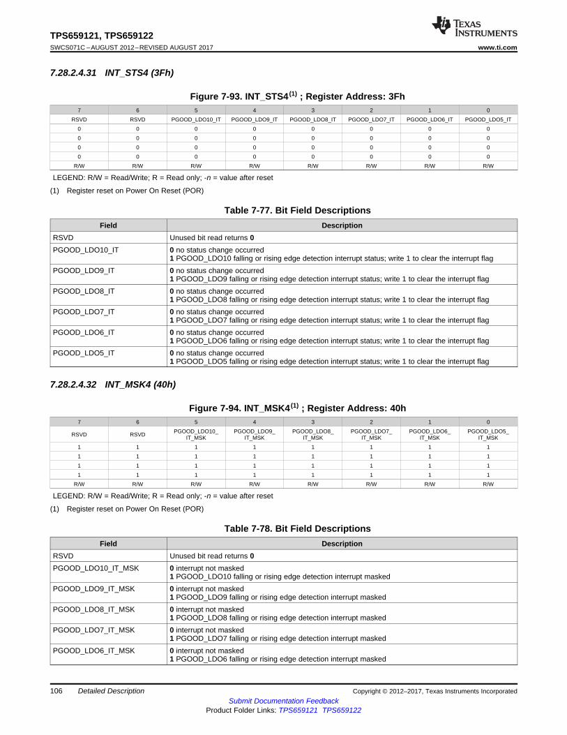
106
TPS659121, TPS659122SWCS071C –AUGUST 2012–REVISED AUGUST 2017 www.ti.com
Submit Documentation FeedbackProduct Folder Links: TPS659121 TPS659122
Detailed Description Copyright © 2012–2017, Texas Instruments Incorporated
7.28.2.4.31 INT_STS4 (3Fh)
(1) Register reset on Power On Reset (POR)
Figure 7-93. INT_STS4 (1) ; Register Address: 3Fh7 6 5 4 3 2 1 0
RSVD RSVD PGOOD_LDO10_IT PGOOD_LDO9_IT PGOOD_LDO8_IT PGOOD_LDO7_IT PGOOD_LDO6_IT PGOOD_LDO5_IT
0 0 0 0 0 0 0 0
0 0 0 0 0 0 0 0
0 0 0 0 0 0 0 0
0 0 0 0 0 0 0 0
R/W R/W R/W R/W R/W R/W R/W R/W
LEGEND: R/W = Read/Write; R = Read only; -n = value after reset
Table 7-77. Bit Field DescriptionsField Description
RSVD Unused bit read returns 0PGOOD_LDO10_IT 0 no status change occurred
1 PGOOD_LDO10 falling or rising edge detection interrupt status; write 1 to clear the interrupt flagPGOOD_LDO9_IT 0 no status change occurred
1 PGOOD_LDO9 falling or rising edge detection interrupt status; write 1 to clear the interrupt flagPGOOD_LDO8_IT 0 no status change occurred
1 PGOOD_LDO8 falling or rising edge detection interrupt status; write 1 to clear the interrupt flagPGOOD_LDO7_IT 0 no status change occurred
1 PGOOD_LDO7 falling or rising edge detection interrupt status; write 1 to clear the interrupt flagPGOOD_LDO6_IT 0 no status change occurred
1 PGOOD_LDO6 falling or rising edge detection interrupt status; write 1 to clear the interrupt flagPGOOD_LDO5_IT 0 no status change occurred
1 PGOOD_LDO5 falling or rising edge detection interrupt status; write 1 to clear the interrupt flag
7.28.2.4.32 INT_MSK4 (40h)
(1) Register reset on Power On Reset (POR)
Figure 7-94. INT_MSK4 (1) ; Register Address: 40h7 6 5 4 3 2 1 0
RSVD RSVD PGOOD_LDO10_IT_MSK
PGOOD_LDO9_IT_MSK
PGOOD_LDO8_IT_MSK
PGOOD_LDO7_IT_MSK
PGOOD_LDO6_IT_MSK
PGOOD_LDO5_IT_MSK
1 1 1 1 1 1 1 1
1 1 1 1 1 1 1 1
1 1 1 1 1 1 1 1
1 1 1 1 1 1 1 1
R/W R/W R/W R/W R/W R/W R/W R/W
LEGEND: R/W = Read/Write; R = Read only; -n = value after reset
Table 7-78. Bit Field DescriptionsField Description
RSVD Unused bit read returns 0PGOOD_LDO10_IT_MSK 0 interrupt not masked
1 PGOOD_LDO10 falling or rising edge detection interrupt maskedPGOOD_LDO9_IT_MSK 0 interrupt not masked
1 PGOOD_LDO9 falling or rising edge detection interrupt maskedPGOOD_LDO8_IT_MSK 0 interrupt not masked
1 PGOOD_LDO8 falling or rising edge detection interrupt maskedPGOOD_LDO7_IT_MSK 0 interrupt not masked
1 PGOOD_LDO7 falling or rising edge detection interrupt maskedPGOOD_LDO6_IT_MSK 0 interrupt not masked
1 PGOOD_LDO6 falling or rising edge detection interrupt masked
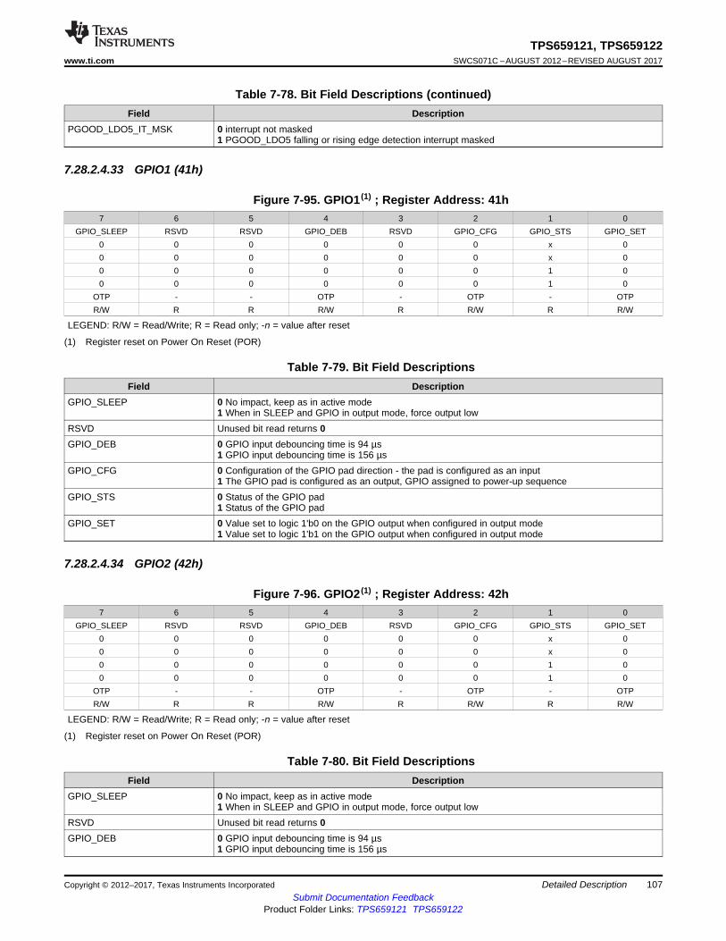
107
TPS659121, TPS659122www.ti.com SWCS071C –AUGUST 2012–REVISED AUGUST 2017
Submit Documentation FeedbackProduct Folder Links: TPS659121 TPS659122
Detailed DescriptionCopyright © 2012–2017, Texas Instruments Incorporated
Table 7-78. Bit Field Descriptions (continued)Field Description
PGOOD_LDO5_IT_MSK 0 interrupt not masked1 PGOOD_LDO5 falling or rising edge detection interrupt masked
7.28.2.4.33 GPIO1 (41h)
(1) Register reset on Power On Reset (POR)
Figure 7-95. GPIO1 (1) ; Register Address: 41h7 6 5 4 3 2 1 0
GPIO_SLEEP RSVD RSVD GPIO_DEB RSVD GPIO_CFG GPIO_STS GPIO_SET0 0 0 0 0 0 x 00 0 0 0 0 0 x 00 0 0 0 0 0 1 00 0 0 0 0 0 1 0
OTP - - OTP - OTP - OTPR/W R R R/W R R/W R R/W
LEGEND: R/W = Read/Write; R = Read only; -n = value after reset
Table 7-79. Bit Field DescriptionsField Description
GPIO_SLEEP 0 No impact, keep as in active mode1 When in SLEEP and GPIO in output mode, force output low
RSVD Unused bit read returns 0GPIO_DEB 0 GPIO input debouncing time is 94 µs
1 GPIO input debouncing time is 156 µsGPIO_CFG 0 Configuration of the GPIO pad direction - the pad is configured as an input
1 The GPIO pad is configured as an output, GPIO assigned to power-up sequenceGPIO_STS 0 Status of the GPIO pad
1 Status of the GPIO padGPIO_SET 0 Value set to logic 1'b0 on the GPIO output when configured in output mode
1 Value set to logic 1'b1 on the GPIO output when configured in output mode
7.28.2.4.34 GPIO2 (42h)
(1) Register reset on Power On Reset (POR)
Figure 7-96. GPIO2 (1) ; Register Address: 42h7 6 5 4 3 2 1 0
GPIO_SLEEP RSVD RSVD GPIO_DEB RSVD GPIO_CFG GPIO_STS GPIO_SET0 0 0 0 0 0 x 00 0 0 0 0 0 x 00 0 0 0 0 0 1 00 0 0 0 0 0 1 0
OTP - - OTP - OTP - OTPR/W R R R/W R R/W R R/W
LEGEND: R/W = Read/Write; R = Read only; -n = value after reset
Table 7-80. Bit Field DescriptionsField Description
GPIO_SLEEP 0 No impact, keep as in active mode1 When in SLEEP and GPIO in output mode, force output low
RSVD Unused bit read returns 0GPIO_DEB 0 GPIO input debouncing time is 94 µs
1 GPIO input debouncing time is 156 µs
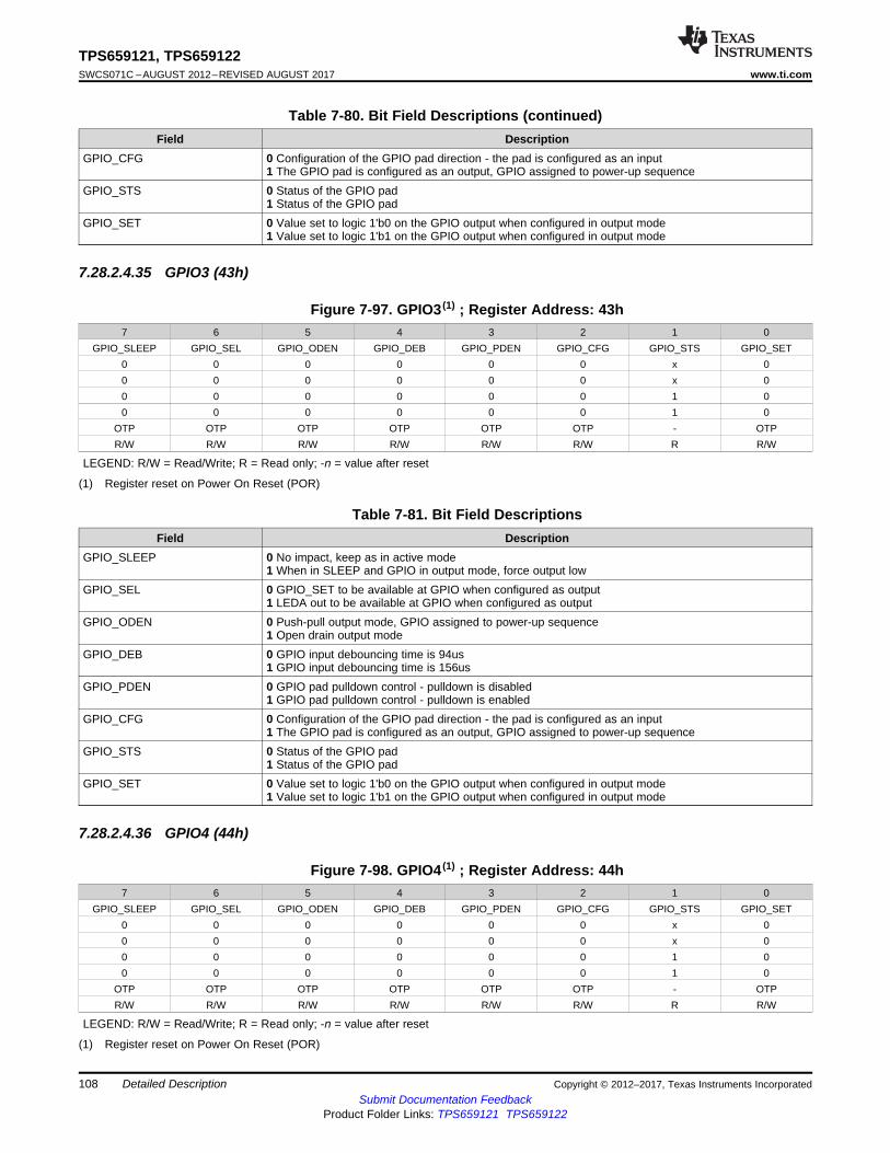
108
TPS659121, TPS659122SWCS071C –AUGUST 2012–REVISED AUGUST 2017 www.ti.com
Submit Documentation FeedbackProduct Folder Links: TPS659121 TPS659122
Detailed Description Copyright © 2012–2017, Texas Instruments Incorporated
Table 7-80. Bit Field Descriptions (continued)Field Description
GPIO_CFG 0 Configuration of the GPIO pad direction - the pad is configured as an input1 The GPIO pad is configured as an output, GPIO assigned to power-up sequence
GPIO_STS 0 Status of the GPIO pad1 Status of the GPIO pad
GPIO_SET 0 Value set to logic 1'b0 on the GPIO output when configured in output mode1 Value set to logic 1'b1 on the GPIO output when configured in output mode
7.28.2.4.35 GPIO3 (43h)
(1) Register reset on Power On Reset (POR)
Figure 7-97. GPIO3 (1) ; Register Address: 43h7 6 5 4 3 2 1 0
GPIO_SLEEP GPIO_SEL GPIO_ODEN GPIO_DEB GPIO_PDEN GPIO_CFG GPIO_STS GPIO_SET0 0 0 0 0 0 x 00 0 0 0 0 0 x 00 0 0 0 0 0 1 00 0 0 0 0 0 1 0
OTP OTP OTP OTP OTP OTP - OTPR/W R/W R/W R/W R/W R/W R R/W
LEGEND: R/W = Read/Write; R = Read only; -n = value after reset
Table 7-81. Bit Field DescriptionsField Description
GPIO_SLEEP 0 No impact, keep as in active mode1 When in SLEEP and GPIO in output mode, force output low
GPIO_SEL 0 GPIO_SET to be available at GPIO when configured as output1 LEDA out to be available at GPIO when configured as output
GPIO_ODEN 0 Push-pull output mode, GPIO assigned to power-up sequence1 Open drain output mode
GPIO_DEB 0 GPIO input debouncing time is 94us1 GPIO input debouncing time is 156us
GPIO_PDEN 0 GPIO pad pulldown control - pulldown is disabled1 GPIO pad pulldown control - pulldown is enabled
GPIO_CFG 0 Configuration of the GPIO pad direction - the pad is configured as an input1 The GPIO pad is configured as an output, GPIO assigned to power-up sequence
GPIO_STS 0 Status of the GPIO pad1 Status of the GPIO pad
GPIO_SET 0 Value set to logic 1'b0 on the GPIO output when configured in output mode1 Value set to logic 1'b1 on the GPIO output when configured in output mode
7.28.2.4.36 GPIO4 (44h)
(1) Register reset on Power On Reset (POR)
Figure 7-98. GPIO4 (1) ; Register Address: 44h7 6 5 4 3 2 1 0
GPIO_SLEEP GPIO_SEL GPIO_ODEN GPIO_DEB GPIO_PDEN GPIO_CFG GPIO_STS GPIO_SET0 0 0 0 0 0 x 00 0 0 0 0 0 x 00 0 0 0 0 0 1 00 0 0 0 0 0 1 0
OTP OTP OTP OTP OTP OTP - OTPR/W R/W R/W R/W R/W R/W R R/W
LEGEND: R/W = Read/Write; R = Read only; -n = value after reset
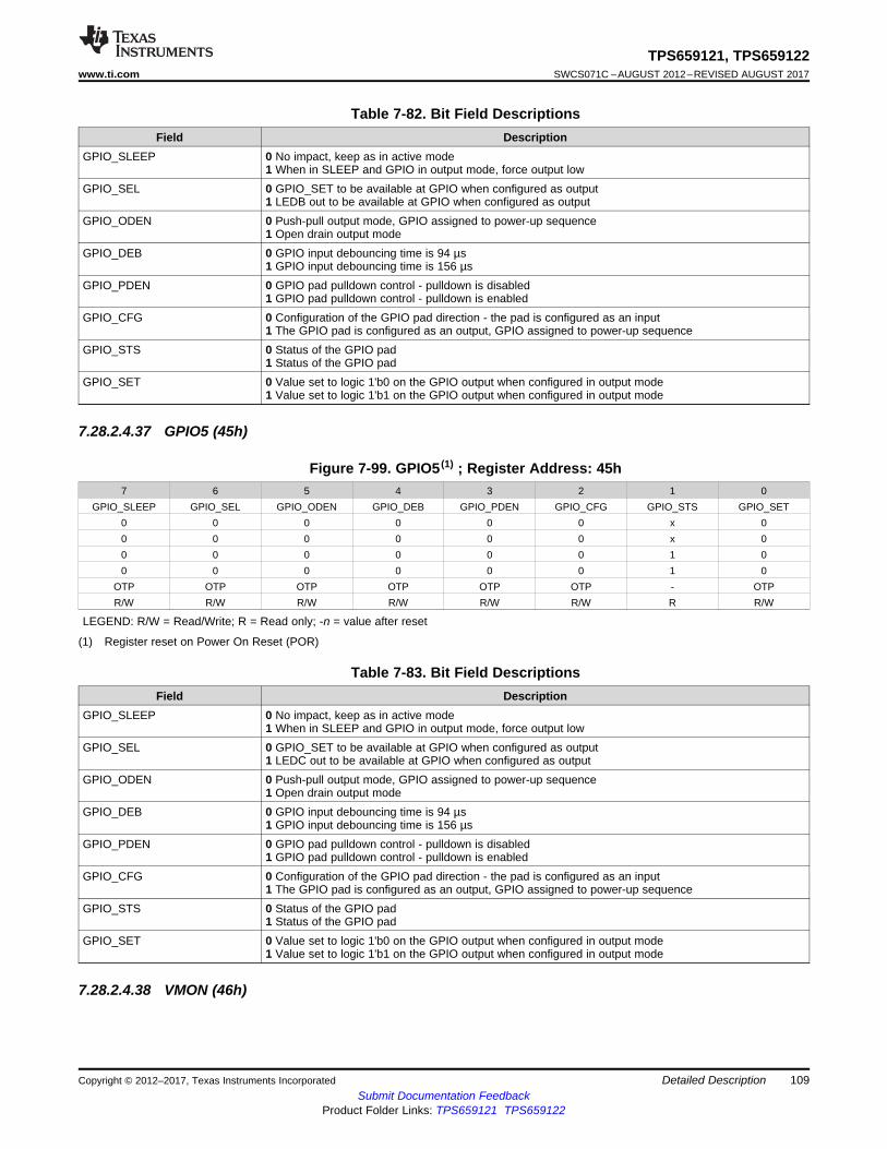
109
TPS659121, TPS659122www.ti.com SWCS071C –AUGUST 2012–REVISED AUGUST 2017
Submit Documentation FeedbackProduct Folder Links: TPS659121 TPS659122
Detailed DescriptionCopyright © 2012–2017, Texas Instruments Incorporated
Table 7-82. Bit Field DescriptionsField Description
GPIO_SLEEP 0 No impact, keep as in active mode1 When in SLEEP and GPIO in output mode, force output low
GPIO_SEL 0 GPIO_SET to be available at GPIO when configured as output1 LEDB out to be available at GPIO when configured as output
GPIO_ODEN 0 Push-pull output mode, GPIO assigned to power-up sequence1 Open drain output mode
GPIO_DEB 0 GPIO input debouncing time is 94 µs1 GPIO input debouncing time is 156 µs
GPIO_PDEN 0 GPIO pad pulldown control - pulldown is disabled1 GPIO pad pulldown control - pulldown is enabled
GPIO_CFG 0 Configuration of the GPIO pad direction - the pad is configured as an input1 The GPIO pad is configured as an output, GPIO assigned to power-up sequence
GPIO_STS 0 Status of the GPIO pad1 Status of the GPIO pad
GPIO_SET 0 Value set to logic 1'b0 on the GPIO output when configured in output mode1 Value set to logic 1'b1 on the GPIO output when configured in output mode
7.28.2.4.37 GPIO5 (45h)
(1) Register reset on Power On Reset (POR)
Figure 7-99. GPIO5 (1) ; Register Address: 45h7 6 5 4 3 2 1 0
GPIO_SLEEP GPIO_SEL GPIO_ODEN GPIO_DEB GPIO_PDEN GPIO_CFG GPIO_STS GPIO_SET0 0 0 0 0 0 x 00 0 0 0 0 0 x 00 0 0 0 0 0 1 00 0 0 0 0 0 1 0
OTP OTP OTP OTP OTP OTP - OTPR/W R/W R/W R/W R/W R/W R R/W
LEGEND: R/W = Read/Write; R = Read only; -n = value after reset
Table 7-83. Bit Field DescriptionsField Description
GPIO_SLEEP 0 No impact, keep as in active mode1 When in SLEEP and GPIO in output mode, force output low
GPIO_SEL 0 GPIO_SET to be available at GPIO when configured as output1 LEDC out to be available at GPIO when configured as output
GPIO_ODEN 0 Push-pull output mode, GPIO assigned to power-up sequence1 Open drain output mode
GPIO_DEB 0 GPIO input debouncing time is 94 µs1 GPIO input debouncing time is 156 µs
GPIO_PDEN 0 GPIO pad pulldown control - pulldown is disabled1 GPIO pad pulldown control - pulldown is enabled
GPIO_CFG 0 Configuration of the GPIO pad direction - the pad is configured as an input1 The GPIO pad is configured as an output, GPIO assigned to power-up sequence
GPIO_STS 0 Status of the GPIO pad1 Status of the GPIO pad
GPIO_SET 0 Value set to logic 1'b0 on the GPIO output when configured in output mode1 Value set to logic 1'b1 on the GPIO output when configured in output mode
7.28.2.4.38 VMON (46h)
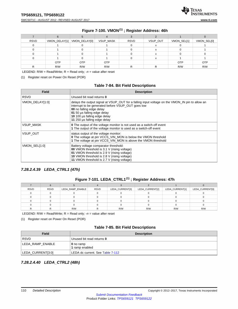
110
TPS659121, TPS659122SWCS071C –AUGUST 2012–REVISED AUGUST 2017 www.ti.com
Submit Documentation FeedbackProduct Folder Links: TPS659121 TPS659122
Detailed Description Copyright © 2012–2017, Texas Instruments Incorporated
(1) Register reset on Power On Reset (POR)
Figure 7-100. VMON (1) ; Register Address: 46h7 6 5 4 3 2 1 0
RSVD VMON_DELAY[1] VMON_DELAY[0] VSUP_MASK RSVD VSUP_OUT VMON_SEL[1] VMON_SEL[0]0 1 0 1 0 x 0 10 1 0 1 0 x 0 10 1 0 1 0 x 0 00 1 0 1 0 x 1 1
OTP OTP OTP OTP OTPR R/W R/W R/W R R R/W R/W
LEGEND: R/W = Read/Write; R = Read only; -n = value after reset
Table 7-84. Bit Field DescriptionsField Description
RSVD Unused bit read returns 0VMON_DELAY[1:0] delays the output signal at VSUP_OUT for a falling input voltage on the VMON_IN pin to allow an
interrupt to be generated before VSUP_OUT goes low00 no falling edge delay01 50 µs falling edge delay10 100 µs falling edge delay11 250 µs falling edge delay
VSUP_MASK 0 The output of the voltage monitor is not used as a switch-off event1 The output of the voltage monitor is used as a switch-off event
VSUP_OUT status output of the voltage monitor:0 The voltage at pin VCCS_VIN_MON is below the VMON threshold1 The voltage at pin VCCS_VIN_MON is above the VMON threshold
VMON_SEL[1:0] Battery voltage comparator threshold:00 VMON threshold is 3.1 V (rising voltage)01 VMON threshold is 2.9 V (rising voltage)10 VMON threshold is 2.8 V (rising voltage)11 VMON threshold is 2.7 V (rising voltage)
7.28.2.4.39 LEDA_CTRL1 (47h)
(1) Register reset on Power On Reset (POR)
Figure 7-101. LEDA_CTRL1 (1) ; Register Address: 47h7 6 5 4 3 2 1 0
RSVD RSVD LEDA_RAMP_ENABLE RSVD LEDA_CURRENT[3] LEDA_CURRENT[2] LEDA_CURRENT[1] LEDA_CURRENT[0]
0 0 0 0 0 0 0 0
0 0 0 0 0 0 0 0
0 0 0 0 0 0 0 0
0 0 0 0 0 0 0 0
R R R/W R R/W R/W R/W R/W
LEGEND: R/W = Read/Write; R = Read only; -n = value after reset
Table 7-85. Bit Field DescriptionsField Description
RSVD Unused bit read returns 0LEDA_RAMP_ENABLE 0 no ramp
1 ramp enabledLEDA_CURRENT[3:0] LEDA dc current. See Table 7-112
7.28.2.4.40 LEDA_CTRL2 (48h)

111
TPS659121, TPS659122www.ti.com SWCS071C –AUGUST 2012–REVISED AUGUST 2017
Submit Documentation FeedbackProduct Folder Links: TPS659121 TPS659122
Detailed DescriptionCopyright © 2012–2017, Texas Instruments Incorporated
(1) Register reset on Power On Reset (POR)
Figure 7-102. LEDA_CTRL2 (1) ; Register Address: 48h7 6 5 4 3 2 1 0
RSVD LEDA_T1[6] LEDA_T1[5] LEDA_T1[4] LEDA_T1[3] LEDA_T1[2] LEDA_T1[1] LEDA_T1[0]0 0 0 0 0 0 0 00 0 0 0 0 0 0 00 0 0 0 0 0 0 00 0 0 0 0 0 0 0R R/W R/W R/W R/W R/W R/W R/W
LEGEND: R/W = Read/Write; R = Read only; -n = value after reset
Table 7-86. Bit Field DescriptionsField Description
RSVD Unused bit read returns 0LEDA_T1[6:0] LEDA T1 sequence length = LEDA_T1[6:0] x 64 ms
0000000 = 0 x 64 ms1111111 = 127 x 64 ms
7.28.2.4.41 LEDA_CTRL3 (49h)
(1) Register reset on Power On Reset (POR)
Figure 7-103. LEDA_CTRL3 (1) ; Register Address: 49h7 6 5 4 3 2 1 0
RSVD LEDA_T2[6] LEDA_T2[5] LEDA_T2[4] LEDA_T2[3] LEDA_T2[2] LEDA_T2[1] LEDA_T2[0]0 0 0 0 0 0 0 00 0 0 0 0 0 0 00 0 0 0 0 0 0 00 0 0 0 0 0 0 0R R/W R/W R/W R/W R/W R/W R/W
LEGEND: R/W = Read/Write; R = Read only; -n = value after reset
Table 7-87. Bit Field DescriptionsField Description
RSVD Unused bit read returns 0LEDA_T2[6:0] LEDA T2 sequence length = LEDA_T2[6:0] x 64 ms
0000000 = 0 x 64 ms1111111 = 127 x 64 ms
7.28.2.4.42 LEDA_CTRL4 (4Ah)
(1) Register reset on Power On Reset (POR)
Figure 7-104. LEDA_CTRL4 (1); Register Address: 4Ah7 6 5 4 3 2 1 0
RSVD LEDA_T3[6] LEDA_T3[5] LEDA_T3[4] LEDA_T3[3] LEDA_T3[2] LEDA_T3[1] LEDA_T3[0]0 0 0 0 0 0 0 00 0 0 0 0 0 0 00 0 0 0 0 0 0 00 0 0 0 0 0 0 0R R/W R/W R/W R/W R/W R/W R/W
LEGEND: R/W = Read/Write; R = Read only; -n = value after reset
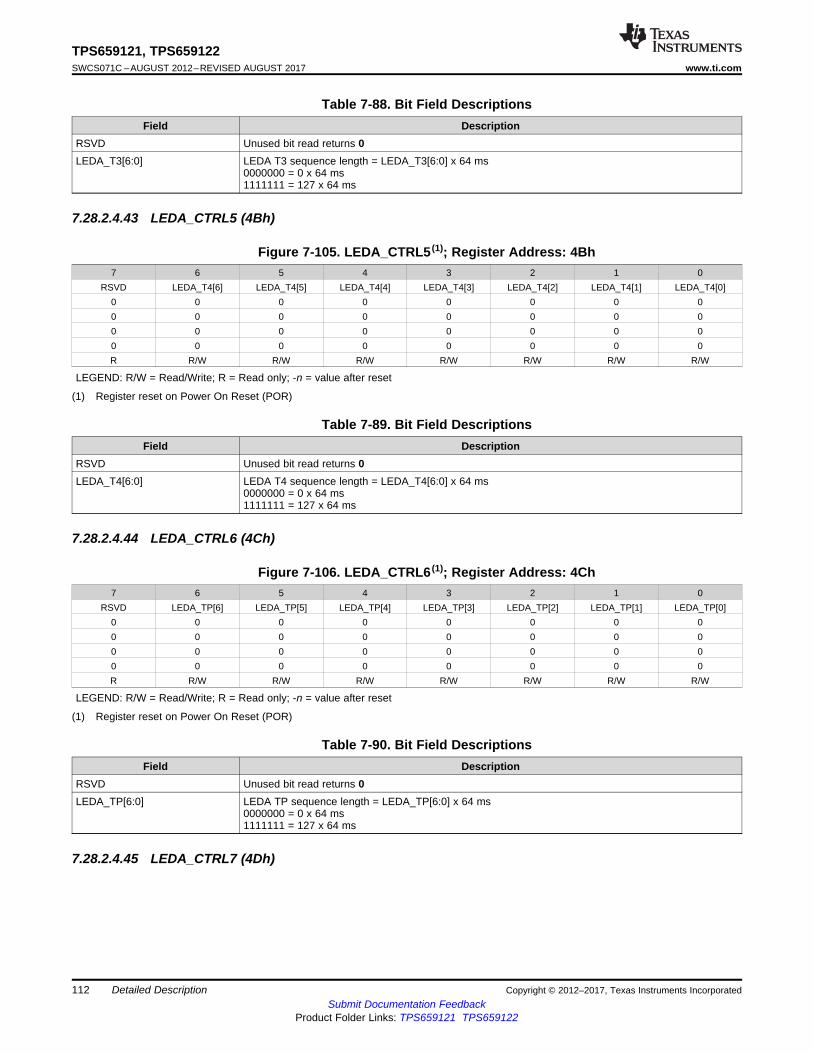
112
TPS659121, TPS659122SWCS071C –AUGUST 2012–REVISED AUGUST 2017 www.ti.com
Submit Documentation FeedbackProduct Folder Links: TPS659121 TPS659122
Detailed Description Copyright © 2012–2017, Texas Instruments Incorporated
Table 7-88. Bit Field DescriptionsField Description
RSVD Unused bit read returns 0LEDA_T3[6:0] LEDA T3 sequence length = LEDA_T3[6:0] x 64 ms
0000000 = 0 x 64 ms1111111 = 127 x 64 ms
7.28.2.4.43 LEDA_CTRL5 (4Bh)
(1) Register reset on Power On Reset (POR)
Figure 7-105. LEDA_CTRL5 (1); Register Address: 4Bh7 6 5 4 3 2 1 0
RSVD LEDA_T4[6] LEDA_T4[5] LEDA_T4[4] LEDA_T4[3] LEDA_T4[2] LEDA_T4[1] LEDA_T4[0]0 0 0 0 0 0 0 00 0 0 0 0 0 0 00 0 0 0 0 0 0 00 0 0 0 0 0 0 0R R/W R/W R/W R/W R/W R/W R/W
LEGEND: R/W = Read/Write; R = Read only; -n = value after reset
Table 7-89. Bit Field DescriptionsField Description
RSVD Unused bit read returns 0LEDA_T4[6:0] LEDA T4 sequence length = LEDA_T4[6:0] x 64 ms
0000000 = 0 x 64 ms1111111 = 127 x 64 ms
7.28.2.4.44 LEDA_CTRL6 (4Ch)
(1) Register reset on Power On Reset (POR)
Figure 7-106. LEDA_CTRL6 (1); Register Address: 4Ch7 6 5 4 3 2 1 0
RSVD LEDA_TP[6] LEDA_TP[5] LEDA_TP[4] LEDA_TP[3] LEDA_TP[2] LEDA_TP[1] LEDA_TP[0]0 0 0 0 0 0 0 00 0 0 0 0 0 0 00 0 0 0 0 0 0 00 0 0 0 0 0 0 0R R/W R/W R/W R/W R/W R/W R/W
LEGEND: R/W = Read/Write; R = Read only; -n = value after reset
Table 7-90. Bit Field DescriptionsField Description
RSVD Unused bit read returns 0LEDA_TP[6:0] LEDA TP sequence length = LEDA_TP[6:0] x 64 ms
0000000 = 0 x 64 ms1111111 = 127 x 64 ms
7.28.2.4.45 LEDA_CTRL7 (4Dh)
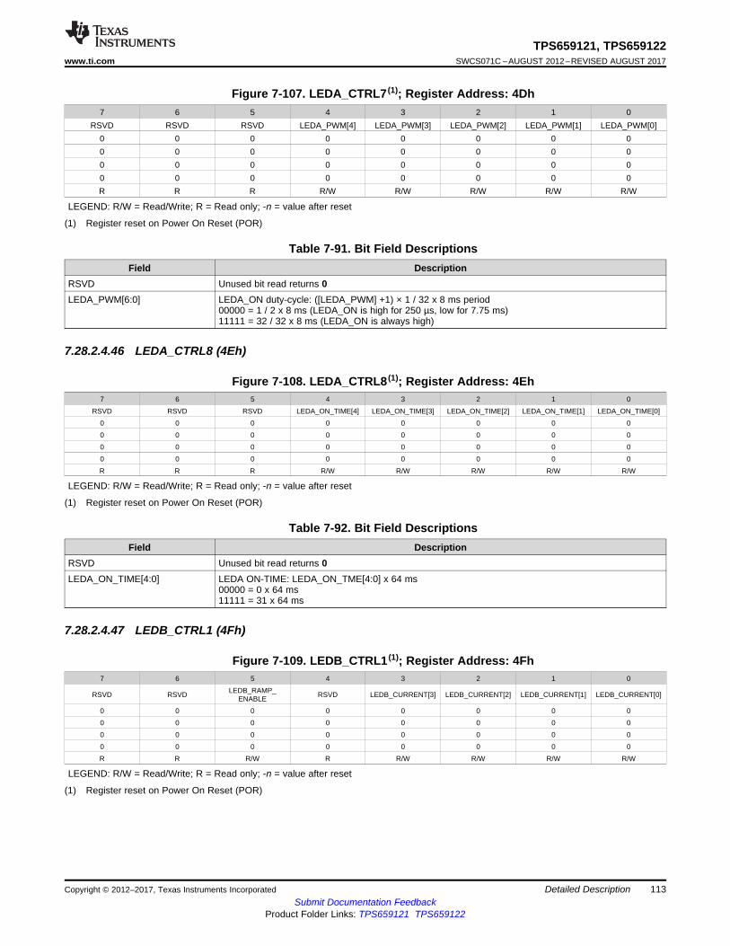
113
TPS659121, TPS659122www.ti.com SWCS071C –AUGUST 2012–REVISED AUGUST 2017
Submit Documentation FeedbackProduct Folder Links: TPS659121 TPS659122
Detailed DescriptionCopyright © 2012–2017, Texas Instruments Incorporated
(1) Register reset on Power On Reset (POR)
Figure 7-107. LEDA_CTRL7 (1); Register Address: 4Dh7 6 5 4 3 2 1 0
RSVD RSVD RSVD LEDA_PWM[4] LEDA_PWM[3] LEDA_PWM[2] LEDA_PWM[1] LEDA_PWM[0]0 0 0 0 0 0 0 00 0 0 0 0 0 0 00 0 0 0 0 0 0 00 0 0 0 0 0 0 0R R R R/W R/W R/W R/W R/W
LEGEND: R/W = Read/Write; R = Read only; -n = value after reset
Table 7-91. Bit Field DescriptionsField Description
RSVD Unused bit read returns 0LEDA_PWM[6:0] LEDA_ON duty-cycle: ([LEDA_PWM] +1) × 1 / 32 x 8 ms period
00000 = 1 / 2 x 8 ms (LEDA_ON is high for 250 µs, low for 7.75 ms)11111 = 32 / 32 x 8 ms (LEDA_ON is always high)
7.28.2.4.46 LEDA_CTRL8 (4Eh)
(1) Register reset on Power On Reset (POR)
Figure 7-108. LEDA_CTRL8 (1); Register Address: 4Eh7 6 5 4 3 2 1 0
RSVD RSVD RSVD LEDA_ON_TIME[4] LEDA_ON_TIME[3] LEDA_ON_TIME[2] LEDA_ON_TIME[1] LEDA_ON_TIME[0]
0 0 0 0 0 0 0 0
0 0 0 0 0 0 0 0
0 0 0 0 0 0 0 0
0 0 0 0 0 0 0 0
R R R R/W R/W R/W R/W R/W
LEGEND: R/W = Read/Write; R = Read only; -n = value after reset
Table 7-92. Bit Field DescriptionsField Description
RSVD Unused bit read returns 0LEDA_ON_TIME[4:0] LEDA ON-TIME: LEDA_ON_TME[4:0] x 64 ms
00000 = 0 x 64 ms11111 = 31 x 64 ms
7.28.2.4.47 LEDB_CTRL1 (4Fh)
(1) Register reset on Power On Reset (POR)
Figure 7-109. LEDB_CTRL1 (1); Register Address: 4Fh7 6 5 4 3 2 1 0
RSVD RSVD LEDB_RAMP_ENABLE RSVD LEDB_CURRENT[3] LEDB_CURRENT[2] LEDB_CURRENT[1] LEDB_CURRENT[0]
0 0 0 0 0 0 0 0
0 0 0 0 0 0 0 0
0 0 0 0 0 0 0 0
0 0 0 0 0 0 0 0
R R R/W R R/W R/W R/W R/W
LEGEND: R/W = Read/Write; R = Read only; -n = value after reset
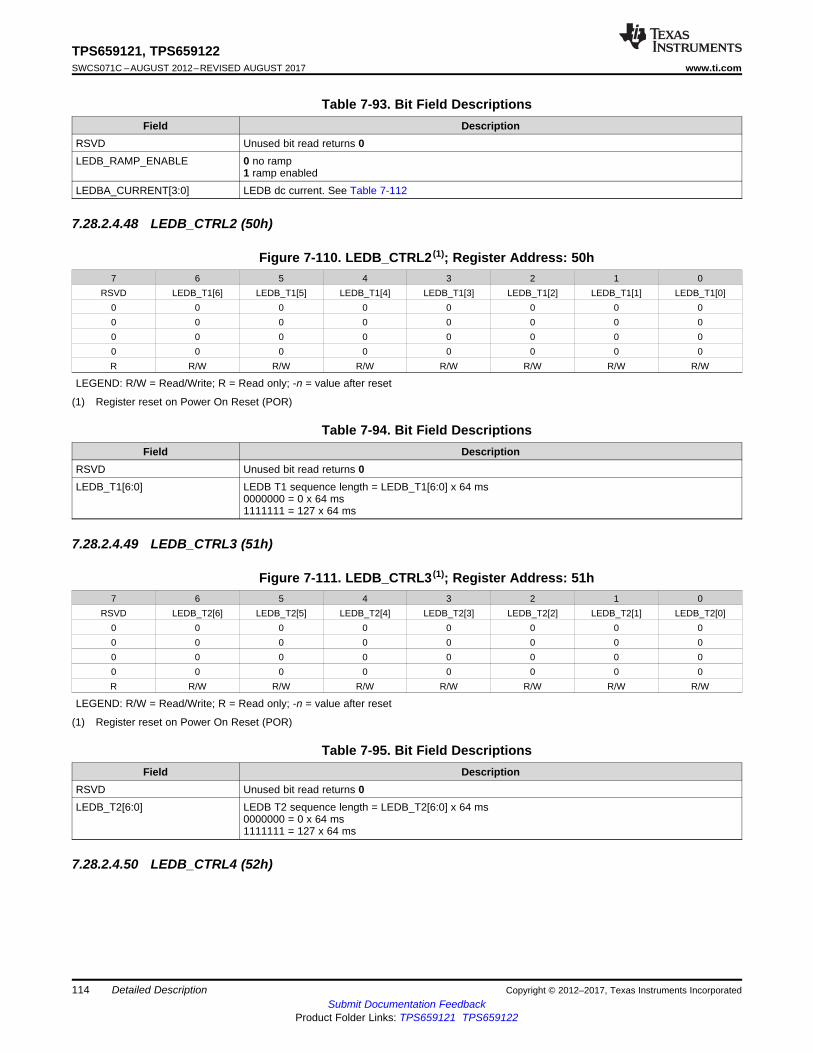
114
TPS659121, TPS659122SWCS071C –AUGUST 2012–REVISED AUGUST 2017 www.ti.com
Submit Documentation FeedbackProduct Folder Links: TPS659121 TPS659122
Detailed Description Copyright © 2012–2017, Texas Instruments Incorporated
Table 7-93. Bit Field DescriptionsField Description
RSVD Unused bit read returns 0LEDB_RAMP_ENABLE 0 no ramp
1 ramp enabledLEDBA_CURRENT[3:0] LEDB dc current. See Table 7-112
7.28.2.4.48 LEDB_CTRL2 (50h)
(1) Register reset on Power On Reset (POR)
Figure 7-110. LEDB_CTRL2 (1); Register Address: 50h7 6 5 4 3 2 1 0
RSVD LEDB_T1[6] LEDB_T1[5] LEDB_T1[4] LEDB_T1[3] LEDB_T1[2] LEDB_T1[1] LEDB_T1[0]0 0 0 0 0 0 0 00 0 0 0 0 0 0 00 0 0 0 0 0 0 00 0 0 0 0 0 0 0R R/W R/W R/W R/W R/W R/W R/W
LEGEND: R/W = Read/Write; R = Read only; -n = value after reset
Table 7-94. Bit Field DescriptionsField Description
RSVD Unused bit read returns 0LEDB_T1[6:0] LEDB T1 sequence length = LEDB_T1[6:0] x 64 ms
0000000 = 0 x 64 ms1111111 = 127 x 64 ms
7.28.2.4.49 LEDB_CTRL3 (51h)
(1) Register reset on Power On Reset (POR)
Figure 7-111. LEDB_CTRL3 (1); Register Address: 51h7 6 5 4 3 2 1 0
RSVD LEDB_T2[6] LEDB_T2[5] LEDB_T2[4] LEDB_T2[3] LEDB_T2[2] LEDB_T2[1] LEDB_T2[0]0 0 0 0 0 0 0 00 0 0 0 0 0 0 00 0 0 0 0 0 0 00 0 0 0 0 0 0 0R R/W R/W R/W R/W R/W R/W R/W
LEGEND: R/W = Read/Write; R = Read only; -n = value after reset
Table 7-95. Bit Field DescriptionsField Description
RSVD Unused bit read returns 0LEDB_T2[6:0] LEDB T2 sequence length = LEDB_T2[6:0] x 64 ms
0000000 = 0 x 64 ms1111111 = 127 x 64 ms
7.28.2.4.50 LEDB_CTRL4 (52h)
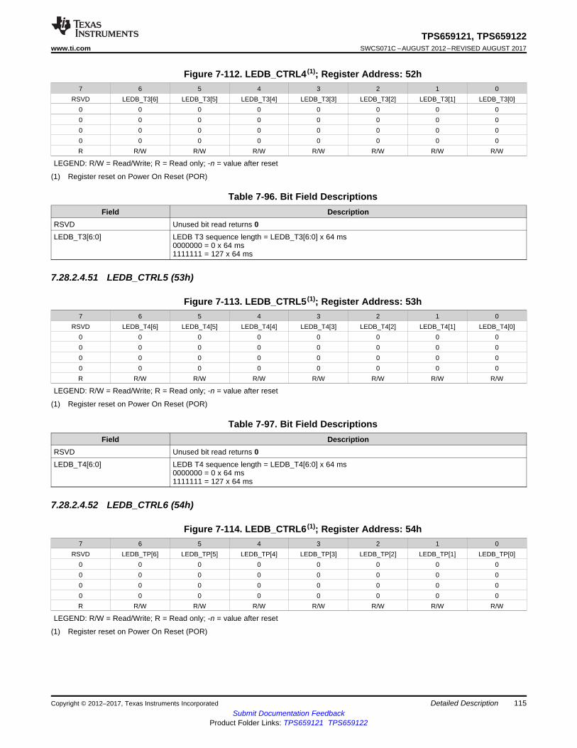
115
TPS659121, TPS659122www.ti.com SWCS071C –AUGUST 2012–REVISED AUGUST 2017
Submit Documentation FeedbackProduct Folder Links: TPS659121 TPS659122
Detailed DescriptionCopyright © 2012–2017, Texas Instruments Incorporated
(1) Register reset on Power On Reset (POR)
Figure 7-112. LEDB_CTRL4 (1); Register Address: 52h7 6 5 4 3 2 1 0
RSVD LEDB_T3[6] LEDB_T3[5] LEDB_T3[4] LEDB_T3[3] LEDB_T3[2] LEDB_T3[1] LEDB_T3[0]0 0 0 0 0 0 0 00 0 0 0 0 0 0 00 0 0 0 0 0 0 00 0 0 0 0 0 0 0R R/W R/W R/W R/W R/W R/W R/W
LEGEND: R/W = Read/Write; R = Read only; -n = value after reset
Table 7-96. Bit Field DescriptionsField Description
RSVD Unused bit read returns 0LEDB_T3[6:0] LEDB T3 sequence length = LEDB_T3[6:0] x 64 ms
0000000 = 0 x 64 ms1111111 = 127 x 64 ms
7.28.2.4.51 LEDB_CTRL5 (53h)
(1) Register reset on Power On Reset (POR)
Figure 7-113. LEDB_CTRL5 (1); Register Address: 53h7 6 5 4 3 2 1 0
RSVD LEDB_T4[6] LEDB_T4[5] LEDB_T4[4] LEDB_T4[3] LEDB_T4[2] LEDB_T4[1] LEDB_T4[0]0 0 0 0 0 0 0 00 0 0 0 0 0 0 00 0 0 0 0 0 0 00 0 0 0 0 0 0 0R R/W R/W R/W R/W R/W R/W R/W
LEGEND: R/W = Read/Write; R = Read only; -n = value after reset
Table 7-97. Bit Field DescriptionsField Description
RSVD Unused bit read returns 0LEDB_T4[6:0] LEDB T4 sequence length = LEDB_T4[6:0] x 64 ms
0000000 = 0 x 64 ms1111111 = 127 x 64 ms
7.28.2.4.52 LEDB_CTRL6 (54h)
(1) Register reset on Power On Reset (POR)
Figure 7-114. LEDB_CTRL6 (1); Register Address: 54h7 6 5 4 3 2 1 0
RSVD LEDB_TP[6] LEDB_TP[5] LEDB_TP[4] LEDB_TP[3] LEDB_TP[2] LEDB_TP[1] LEDB_TP[0]0 0 0 0 0 0 0 00 0 0 0 0 0 0 00 0 0 0 0 0 0 00 0 0 0 0 0 0 0R R/W R/W R/W R/W R/W R/W R/W
LEGEND: R/W = Read/Write; R = Read only; -n = value after reset
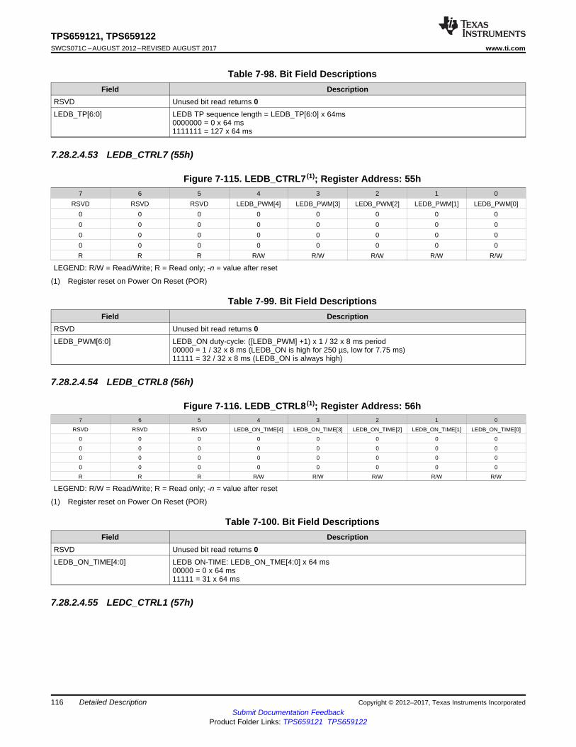
116
TPS659121, TPS659122SWCS071C –AUGUST 2012–REVISED AUGUST 2017 www.ti.com
Submit Documentation FeedbackProduct Folder Links: TPS659121 TPS659122
Detailed Description Copyright © 2012–2017, Texas Instruments Incorporated
Table 7-98. Bit Field DescriptionsField Description
RSVD Unused bit read returns 0LEDB_TP[6:0] LEDB TP sequence length = LEDB_TP[6:0] x 64ms
0000000 = 0 x 64 ms1111111 = 127 x 64 ms
7.28.2.4.53 LEDB_CTRL7 (55h)
(1) Register reset on Power On Reset (POR)
Figure 7-115. LEDB_CTRL7 (1); Register Address: 55h7 6 5 4 3 2 1 0
RSVD RSVD RSVD LEDB_PWM[4] LEDB_PWM[3] LEDB_PWM[2] LEDB_PWM[1] LEDB_PWM[0]0 0 0 0 0 0 0 00 0 0 0 0 0 0 00 0 0 0 0 0 0 00 0 0 0 0 0 0 0R R R R/W R/W R/W R/W R/W
LEGEND: R/W = Read/Write; R = Read only; -n = value after reset
Table 7-99. Bit Field DescriptionsField Description
RSVD Unused bit read returns 0LEDB_PWM[6:0] LEDB_ON duty-cycle: ([LEDB_PWM] +1) x 1 / 32 x 8 ms period
00000 = 1 / 32 x 8 ms (LEDB_ON is high for 250 µs, low for 7.75 ms)11111 = 32 / 32 x 8 ms (LEDB_ON is always high)
7.28.2.4.54 LEDB_CTRL8 (56h)
(1) Register reset on Power On Reset (POR)
Figure 7-116. LEDB_CTRL8 (1); Register Address: 56h7 6 5 4 3 2 1 0
RSVD RSVD RSVD LEDB_ON_TIME[4] LEDB_ON_TIME[3] LEDB_ON_TIME[2] LEDB_ON_TIME[1] LEDB_ON_TIME[0]
0 0 0 0 0 0 0 0
0 0 0 0 0 0 0 0
0 0 0 0 0 0 0 0
0 0 0 0 0 0 0 0
R R R R/W R/W R/W R/W R/W
LEGEND: R/W = Read/Write; R = Read only; -n = value after reset
Table 7-100. Bit Field DescriptionsField Description
RSVD Unused bit read returns 0LEDB_ON_TIME[4:0] LEDB ON-TIME: LEDB_ON_TME[4:0] x 64 ms
00000 = 0 x 64 ms11111 = 31 x 64 ms
7.28.2.4.55 LEDC_CTRL1 (57h)
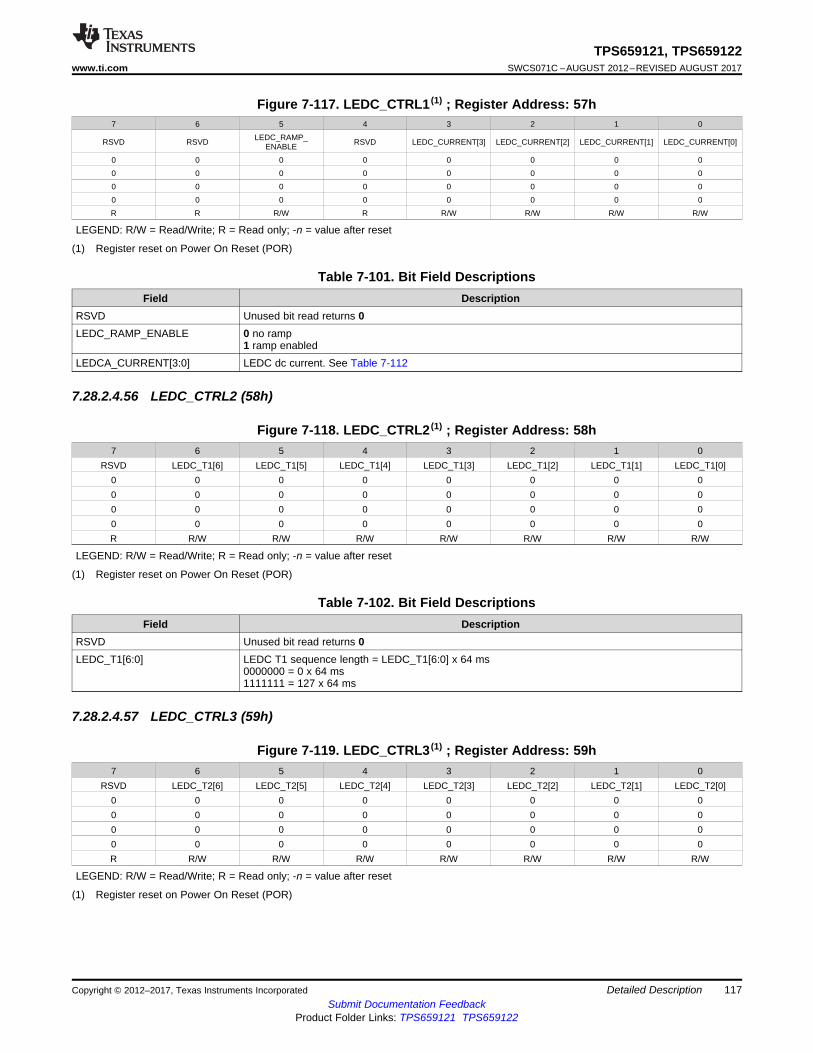
117
TPS659121, TPS659122www.ti.com SWCS071C –AUGUST 2012–REVISED AUGUST 2017
Submit Documentation FeedbackProduct Folder Links: TPS659121 TPS659122
Detailed DescriptionCopyright © 2012–2017, Texas Instruments Incorporated
(1) Register reset on Power On Reset (POR)
Figure 7-117. LEDC_CTRL1 (1) ; Register Address: 57h7 6 5 4 3 2 1 0
RSVD RSVD LEDC_RAMP_ENABLE RSVD LEDC_CURRENT[3] LEDC_CURRENT[2] LEDC_CURRENT[1] LEDC_CURRENT[0]
0 0 0 0 0 0 0 0
0 0 0 0 0 0 0 0
0 0 0 0 0 0 0 0
0 0 0 0 0 0 0 0
R R R/W R R/W R/W R/W R/W
LEGEND: R/W = Read/Write; R = Read only; -n = value after reset
Table 7-101. Bit Field DescriptionsField Description
RSVD Unused bit read returns 0LEDC_RAMP_ENABLE 0 no ramp
1 ramp enabledLEDCA_CURRENT[3:0] LEDC dc current. See Table 7-112
7.28.2.4.56 LEDC_CTRL2 (58h)
(1) Register reset on Power On Reset (POR)
Figure 7-118. LEDC_CTRL2 (1) ; Register Address: 58h7 6 5 4 3 2 1 0
RSVD LEDC_T1[6] LEDC_T1[5] LEDC_T1[4] LEDC_T1[3] LEDC_T1[2] LEDC_T1[1] LEDC_T1[0]0 0 0 0 0 0 0 00 0 0 0 0 0 0 00 0 0 0 0 0 0 00 0 0 0 0 0 0 0R R/W R/W R/W R/W R/W R/W R/W
LEGEND: R/W = Read/Write; R = Read only; -n = value after reset
Table 7-102. Bit Field DescriptionsField Description
RSVD Unused bit read returns 0LEDC_T1[6:0] LEDC T1 sequence length = LEDC_T1[6:0] x 64 ms
0000000 = 0 x 64 ms1111111 = 127 x 64 ms
7.28.2.4.57 LEDC_CTRL3 (59h)
(1) Register reset on Power On Reset (POR)
Figure 7-119. LEDC_CTRL3 (1) ; Register Address: 59h7 6 5 4 3 2 1 0
RSVD LEDC_T2[6] LEDC_T2[5] LEDC_T2[4] LEDC_T2[3] LEDC_T2[2] LEDC_T2[1] LEDC_T2[0]0 0 0 0 0 0 0 00 0 0 0 0 0 0 00 0 0 0 0 0 0 00 0 0 0 0 0 0 0R R/W R/W R/W R/W R/W R/W R/W
LEGEND: R/W = Read/Write; R = Read only; -n = value after reset
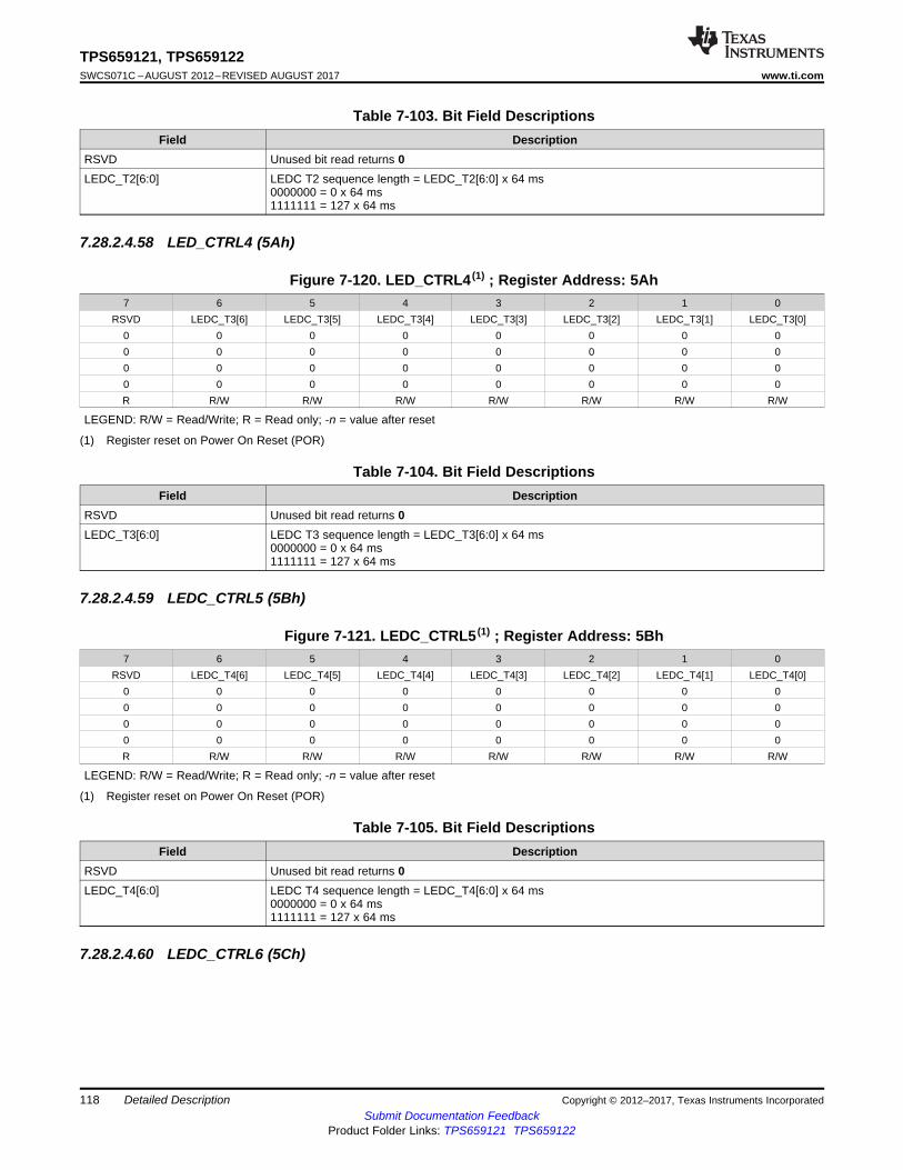
118
TPS659121, TPS659122SWCS071C –AUGUST 2012–REVISED AUGUST 2017 www.ti.com
Submit Documentation FeedbackProduct Folder Links: TPS659121 TPS659122
Detailed Description Copyright © 2012–2017, Texas Instruments Incorporated
Table 7-103. Bit Field DescriptionsField Description
RSVD Unused bit read returns 0LEDC_T2[6:0] LEDC T2 sequence length = LEDC_T2[6:0] x 64 ms
0000000 = 0 x 64 ms1111111 = 127 x 64 ms
7.28.2.4.58 LED_CTRL4 (5Ah)
(1) Register reset on Power On Reset (POR)
Figure 7-120. LED_CTRL4 (1) ; Register Address: 5Ah7 6 5 4 3 2 1 0
RSVD LEDC_T3[6] LEDC_T3[5] LEDC_T3[4] LEDC_T3[3] LEDC_T3[2] LEDC_T3[1] LEDC_T3[0]0 0 0 0 0 0 0 00 0 0 0 0 0 0 00 0 0 0 0 0 0 00 0 0 0 0 0 0 0R R/W R/W R/W R/W R/W R/W R/W
LEGEND: R/W = Read/Write; R = Read only; -n = value after reset
Table 7-104. Bit Field DescriptionsField Description
RSVD Unused bit read returns 0LEDC_T3[6:0] LEDC T3 sequence length = LEDC_T3[6:0] x 64 ms
0000000 = 0 x 64 ms1111111 = 127 x 64 ms
7.28.2.4.59 LEDC_CTRL5 (5Bh)
(1) Register reset on Power On Reset (POR)
Figure 7-121. LEDC_CTRL5 (1) ; Register Address: 5Bh7 6 5 4 3 2 1 0
RSVD LEDC_T4[6] LEDC_T4[5] LEDC_T4[4] LEDC_T4[3] LEDC_T4[2] LEDC_T4[1] LEDC_T4[0]0 0 0 0 0 0 0 00 0 0 0 0 0 0 00 0 0 0 0 0 0 00 0 0 0 0 0 0 0R R/W R/W R/W R/W R/W R/W R/W
LEGEND: R/W = Read/Write; R = Read only; -n = value after reset
Table 7-105. Bit Field DescriptionsField Description
RSVD Unused bit read returns 0LEDC_T4[6:0] LEDC T4 sequence length = LEDC_T4[6:0] x 64 ms
0000000 = 0 x 64 ms1111111 = 127 x 64 ms
7.28.2.4.60 LEDC_CTRL6 (5Ch)
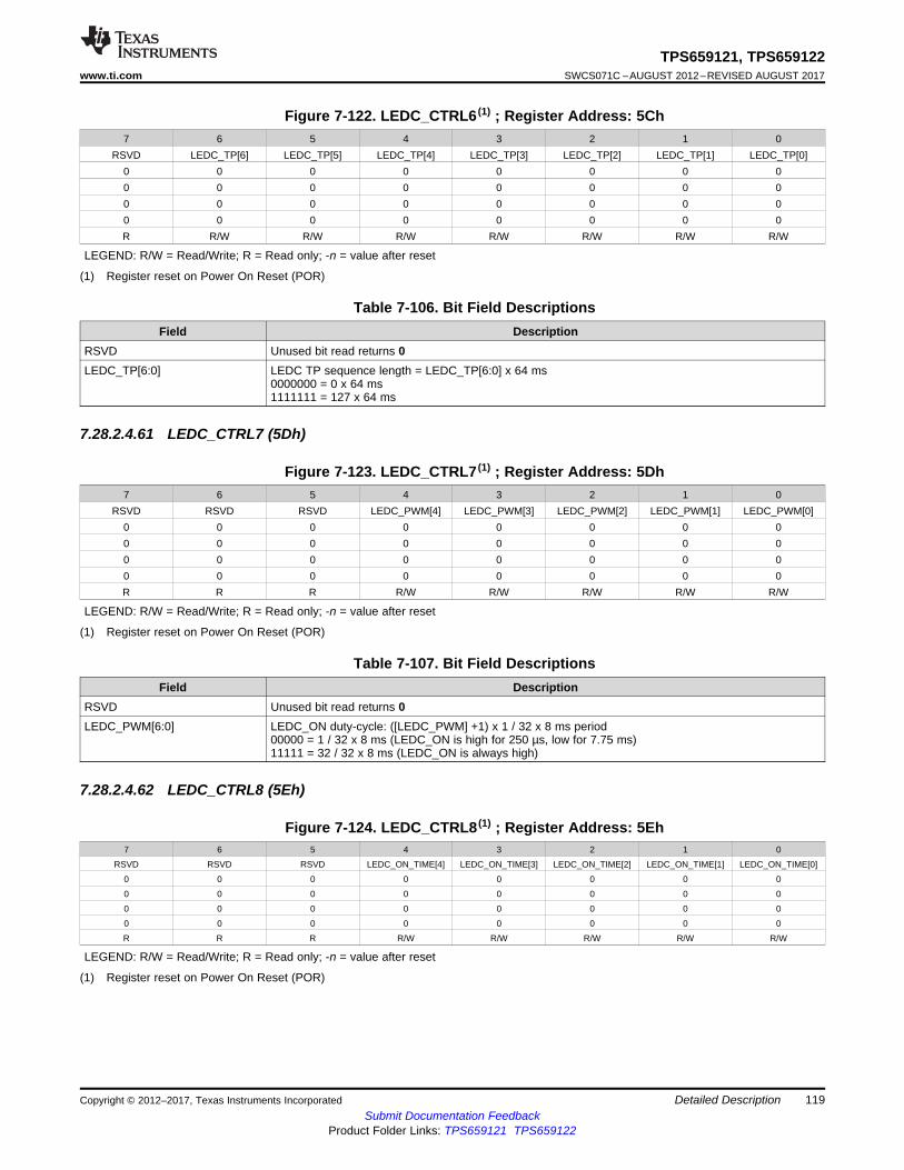
119
TPS659121, TPS659122www.ti.com SWCS071C –AUGUST 2012–REVISED AUGUST 2017
Submit Documentation FeedbackProduct Folder Links: TPS659121 TPS659122
Detailed DescriptionCopyright © 2012–2017, Texas Instruments Incorporated
(1) Register reset on Power On Reset (POR)
Figure 7-122. LEDC_CTRL6 (1) ; Register Address: 5Ch7 6 5 4 3 2 1 0
RSVD LEDC_TP[6] LEDC_TP[5] LEDC_TP[4] LEDC_TP[3] LEDC_TP[2] LEDC_TP[1] LEDC_TP[0]0 0 0 0 0 0 0 00 0 0 0 0 0 0 00 0 0 0 0 0 0 00 0 0 0 0 0 0 0R R/W R/W R/W R/W R/W R/W R/W
LEGEND: R/W = Read/Write; R = Read only; -n = value after reset
Table 7-106. Bit Field DescriptionsField Description
RSVD Unused bit read returns 0LEDC_TP[6:0] LEDC TP sequence length = LEDC_TP[6:0] x 64 ms
0000000 = 0 x 64 ms1111111 = 127 x 64 ms
7.28.2.4.61 LEDC_CTRL7 (5Dh)
(1) Register reset on Power On Reset (POR)
Figure 7-123. LEDC_CTRL7 (1) ; Register Address: 5Dh7 6 5 4 3 2 1 0
RSVD RSVD RSVD LEDC_PWM[4] LEDC_PWM[3] LEDC_PWM[2] LEDC_PWM[1] LEDC_PWM[0]0 0 0 0 0 0 0 00 0 0 0 0 0 0 00 0 0 0 0 0 0 00 0 0 0 0 0 0 0R R R R/W R/W R/W R/W R/W
LEGEND: R/W = Read/Write; R = Read only; -n = value after reset
Table 7-107. Bit Field DescriptionsField Description
RSVD Unused bit read returns 0LEDC_PWM[6:0] LEDC_ON duty-cycle: ([LEDC_PWM] +1) x 1 / 32 x 8 ms period
00000 = 1 / 32 x 8 ms (LEDC_ON is high for 250 µs, low for 7.75 ms)11111 = 32 / 32 x 8 ms (LEDC_ON is always high)
7.28.2.4.62 LEDC_CTRL8 (5Eh)
(1) Register reset on Power On Reset (POR)
Figure 7-124. LEDC_CTRL8 (1) ; Register Address: 5Eh7 6 5 4 3 2 1 0
RSVD RSVD RSVD LEDC_ON_TIME[4] LEDC_ON_TIME[3] LEDC_ON_TIME[2] LEDC_ON_TIME[1] LEDC_ON_TIME[0]
0 0 0 0 0 0 0 0
0 0 0 0 0 0 0 0
0 0 0 0 0 0 0 0
0 0 0 0 0 0 0 0
R R R R/W R/W R/W R/W R/W
LEGEND: R/W = Read/Write; R = Read only; -n = value after reset
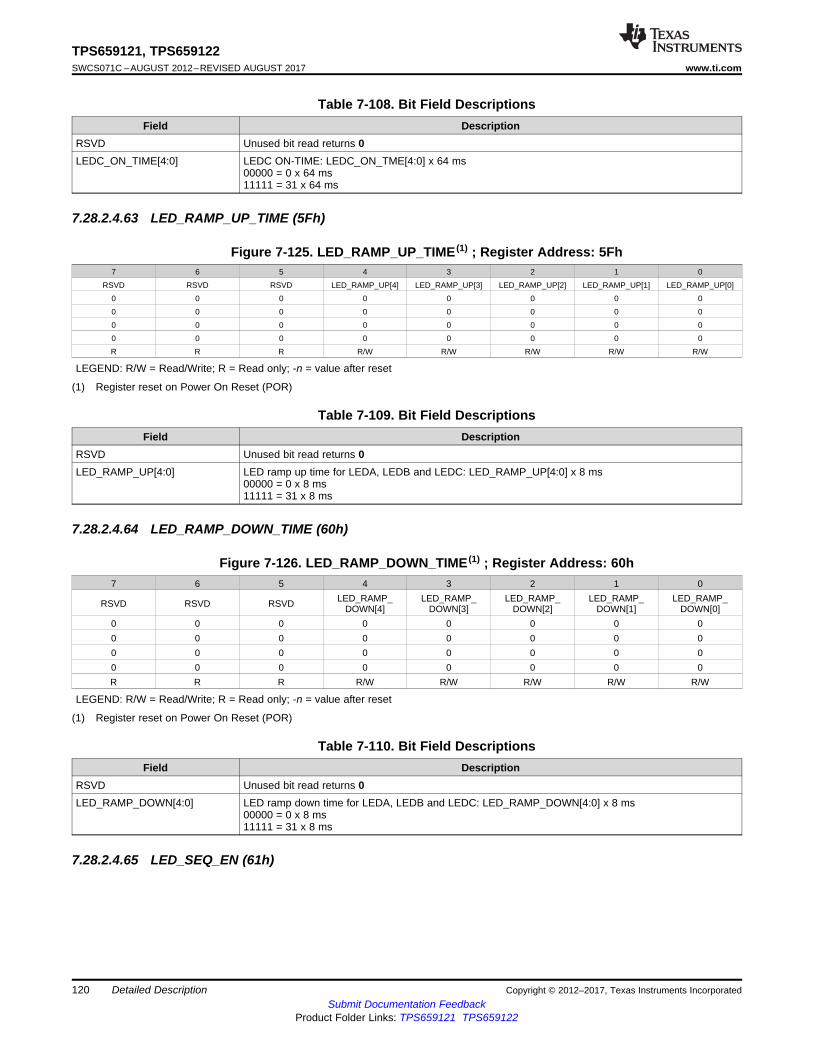
120
TPS659121, TPS659122SWCS071C –AUGUST 2012–REVISED AUGUST 2017 www.ti.com
Submit Documentation FeedbackProduct Folder Links: TPS659121 TPS659122
Detailed Description Copyright © 2012–2017, Texas Instruments Incorporated
Table 7-108. Bit Field DescriptionsField Description
RSVD Unused bit read returns 0LEDC_ON_TIME[4:0] LEDC ON-TIME: LEDC_ON_TME[4:0] x 64 ms
00000 = 0 x 64 ms11111 = 31 x 64 ms
7.28.2.4.63 LED_RAMP_UP_TIME (5Fh)
(1) Register reset on Power On Reset (POR)
Figure 7-125. LED_RAMP_UP_TIME (1) ; Register Address: 5Fh7 6 5 4 3 2 1 0
RSVD RSVD RSVD LED_RAMP_UP[4] LED_RAMP_UP[3] LED_RAMP_UP[2] LED_RAMP_UP[1] LED_RAMP_UP[0]
0 0 0 0 0 0 0 0
0 0 0 0 0 0 0 0
0 0 0 0 0 0 0 0
0 0 0 0 0 0 0 0
R R R R/W R/W R/W R/W R/W
LEGEND: R/W = Read/Write; R = Read only; -n = value after reset
Table 7-109. Bit Field DescriptionsField Description
RSVD Unused bit read returns 0LED_RAMP_UP[4:0] LED ramp up time for LEDA, LEDB and LEDC: LED_RAMP_UP[4:0] x 8 ms
00000 = 0 x 8 ms11111 = 31 x 8 ms
7.28.2.4.64 LED_RAMP_DOWN_TIME (60h)
(1) Register reset on Power On Reset (POR)
Figure 7-126. LED_RAMP_DOWN_TIME (1) ; Register Address: 60h7 6 5 4 3 2 1 0
RSVD RSVD RSVD LED_RAMP_DOWN[4]
LED_RAMP_DOWN[3]
LED_RAMP_DOWN[2]
LED_RAMP_DOWN[1]
LED_RAMP_DOWN[0]
0 0 0 0 0 0 0 00 0 0 0 0 0 0 00 0 0 0 0 0 0 00 0 0 0 0 0 0 0R R R R/W R/W R/W R/W R/W
LEGEND: R/W = Read/Write; R = Read only; -n = value after reset
Table 7-110. Bit Field DescriptionsField Description
RSVD Unused bit read returns 0LED_RAMP_DOWN[4:0] LED ramp down time for LEDA, LEDB and LEDC: LED_RAMP_DOWN[4:0] x 8 ms
00000 = 0 x 8 ms11111 = 31 x 8 ms
7.28.2.4.65 LED_SEQ_EN (61h)
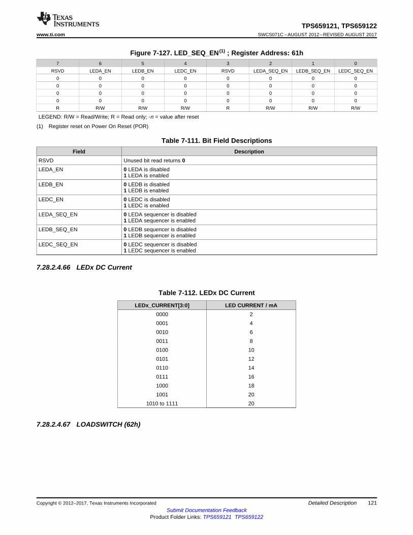
121
TPS659121, TPS659122www.ti.com SWCS071C –AUGUST 2012–REVISED AUGUST 2017
Submit Documentation FeedbackProduct Folder Links: TPS659121 TPS659122
Detailed DescriptionCopyright © 2012–2017, Texas Instruments Incorporated
(1) Register reset on Power On Reset (POR)
Figure 7-127. LED_SEQ_EN (1) ; Register Address: 61h7 6 5 4 3 2 1 0
RSVD LEDA_EN LEDB_EN LEDC_EN RSVD LEDA_SEQ_EN LEDB_SEQ_EN LEDC_SEQ_EN0 0 0 0 0 0 0 00 0 0 0 0 0 0 00 0 0 0 0 0 0 00 0 0 0 0 0 0 0R R/W R/W R/W R R/W R/W R/W
LEGEND: R/W = Read/Write; R = Read only; -n = value after reset
Table 7-111. Bit Field DescriptionsField Description
RSVD Unused bit read returns 0LEDA_EN 0 LEDA is disabled
1 LEDA is enabledLEDB_EN 0 LEDB is disabled
1 LEDB is enabledLEDC_EN 0 LEDC is disabled
1 LEDC is enabledLEDA_SEQ_EN 0 LEDA sequencer is disabled
1 LEDA sequencer is enabledLEDB_SEQ_EN 0 LEDB sequencer is disabled
1 LEDB sequencer is enabledLEDC_SEQ_EN 0 LEDC sequencer is disabled
1 LEDC sequencer is enabled
7.28.2.4.66 LEDx DC Current
Table 7-112. LEDx DC Current
LEDx_CURRENT[3:0] LED CURRENT / mA0000 20001 40010 60011 80100 100101 120110 140111 161000 181001 20
1010 to 1111 20
7.28.2.4.67 LOADSWITCH (62h)
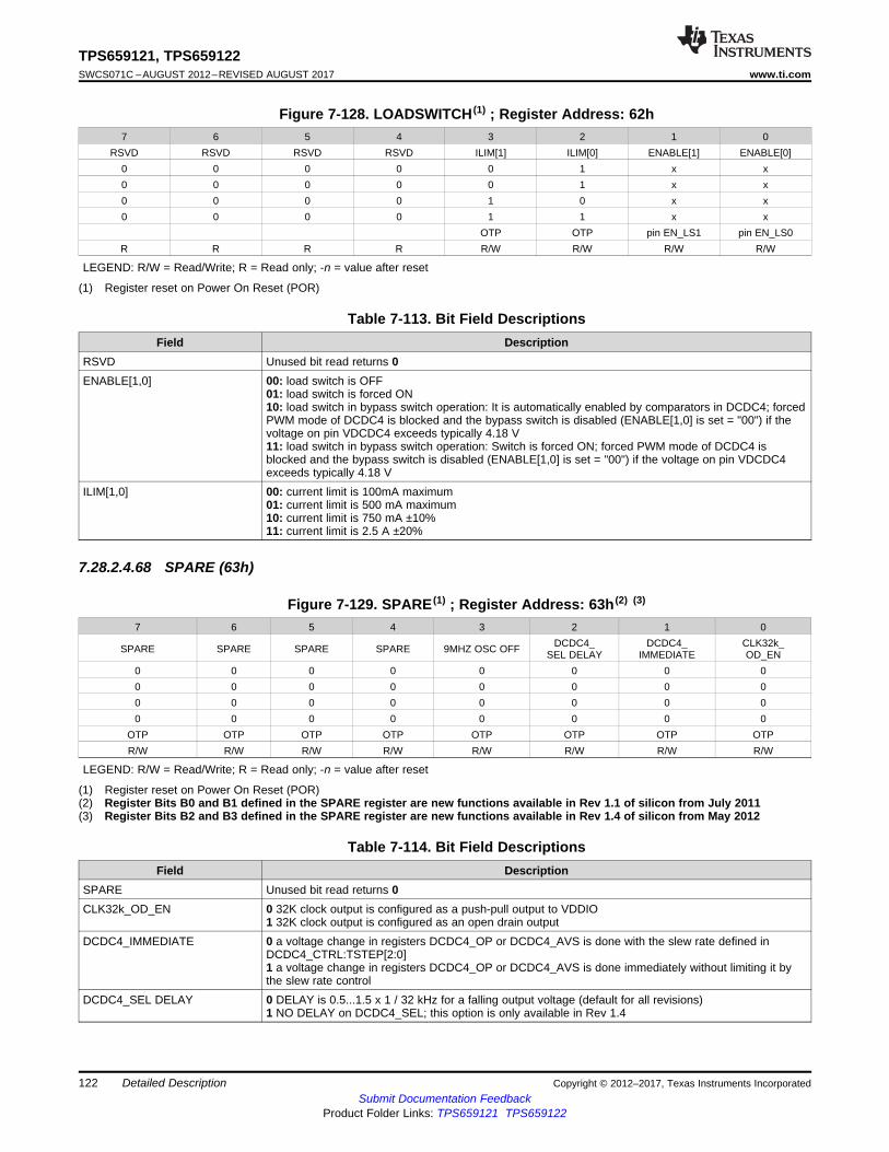
122
TPS659121, TPS659122SWCS071C –AUGUST 2012–REVISED AUGUST 2017 www.ti.com
Submit Documentation FeedbackProduct Folder Links: TPS659121 TPS659122
Detailed Description Copyright © 2012–2017, Texas Instruments Incorporated
(1) Register reset on Power On Reset (POR)
Figure 7-128. LOADSWITCH (1) ; Register Address: 62h7 6 5 4 3 2 1 0
RSVD RSVD RSVD RSVD ILIM[1] ILIM[0] ENABLE[1] ENABLE[0]0 0 0 0 0 1 x x0 0 0 0 0 1 x x0 0 0 0 1 0 x x0 0 0 0 1 1 x x
OTP OTP pin EN_LS1 pin EN_LS0R R R R R/W R/W R/W R/W
LEGEND: R/W = Read/Write; R = Read only; -n = value after reset
Table 7-113. Bit Field DescriptionsField Description
RSVD Unused bit read returns 0ENABLE[1,0] 00: load switch is OFF
01: load switch is forced ON10: load switch in bypass switch operation: It is automatically enabled by comparators in DCDC4; forcedPWM mode of DCDC4 is blocked and the bypass switch is disabled (ENABLE[1,0] is set = "00") if thevoltage on pin VDCDC4 exceeds typically 4.18 V11: load switch in bypass switch operation: Switch is forced ON; forced PWM mode of DCDC4 isblocked and the bypass switch is disabled (ENABLE[1,0] is set = "00") if the voltage on pin VDCDC4exceeds typically 4.18 V
ILIM[1,0] 00: current limit is 100mA maximum01: current limit is 500 mA maximum10: current limit is 750 mA ±10%11: current limit is 2.5 A ±20%
7.28.2.4.68 SPARE (63h)
(1) Register reset on Power On Reset (POR)(2) Register Bits B0 and B1 defined in the SPARE register are new functions available in Rev 1.1 of silicon from July 2011(3) Register Bits B2 and B3 defined in the SPARE register are new functions available in Rev 1.4 of silicon from May 2012
Figure 7-129. SPARE (1) ; Register Address: 63h (2) (3)
7 6 5 4 3 2 1 0
SPARE SPARE SPARE SPARE 9MHZ OSC OFF DCDC4_SEL DELAY
DCDC4_IMMEDIATE
CLK32k_OD_EN
0 0 0 0 0 0 0 00 0 0 0 0 0 0 00 0 0 0 0 0 0 00 0 0 0 0 0 0 0
OTP OTP OTP OTP OTP OTP OTP OTPR/W R/W R/W R/W R/W R/W R/W R/W
LEGEND: R/W = Read/Write; R = Read only; -n = value after reset
Table 7-114. Bit Field DescriptionsField Description
SPARE Unused bit read returns 0CLK32k_OD_EN 0 32K clock output is configured as a push-pull output to VDDIO
1 32K clock output is configured as an open drain outputDCDC4_IMMEDIATE 0 a voltage change in registers DCDC4_OP or DCDC4_AVS is done with the slew rate defined in
DCDC4_CTRL:TSTEP[2:0]1 a voltage change in registers DCDC4_OP or DCDC4_AVS is done immediately without limiting it bythe slew rate control
DCDC4_SEL DELAY 0 DELAY is 0.5...1.5 x 1 / 32 kHz for a falling output voltage (default for all revisions)1 NO DELAY on DCDC4_SEL; this option is only available in Rev 1.4
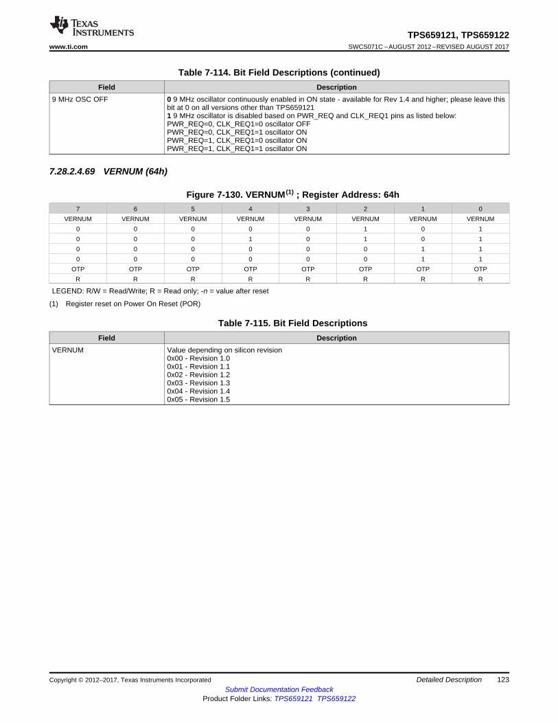
123
TPS659121, TPS659122www.ti.com SWCS071C –AUGUST 2012–REVISED AUGUST 2017
Submit Documentation FeedbackProduct Folder Links: TPS659121 TPS659122
Detailed DescriptionCopyright © 2012–2017, Texas Instruments Incorporated
Table 7-114. Bit Field Descriptions (continued)Field Description
9 MHz OSC OFF 0 9 MHz oscillator continuously enabled in ON state - available for Rev 1.4 and higher; please leave thisbit at 0 on all versions other than TPS6591211 9 MHz oscillator is disabled based on PWR_REQ and CLK_REQ1 pins as listed below:PWR_REQ=0, CLK_REQ1=0 oscillator OFFPWR_REQ=0, CLK_REQ1=1 oscillator ONPWR_REQ=1, CLK_REQ1=0 oscillator ONPWR_REQ=1, CLK_REQ1=1 oscillator ON
7.28.2.4.69 VERNUM (64h)
(1) Register reset on Power On Reset (POR)
Figure 7-130. VERNUM (1) ; Register Address: 64h7 6 5 4 3 2 1 0
VERNUM VERNUM VERNUM VERNUM VERNUM VERNUM VERNUM VERNUM0 0 0 0 0 1 0 10 0 0 1 0 1 0 10 0 0 0 0 0 1 10 0 0 0 0 0 1 1
OTP OTP OTP OTP OTP OTP OTP OTPR R R R R R R R
LEGEND: R/W = Read/Write; R = Read only; -n = value after reset
Table 7-115. Bit Field DescriptionsField Description
VERNUM Value depending on silicon revision0x00 - Revision 1.00x01 - Revision 1.10x02 - Revision 1.20x03 - Revision 1.30x04 - Revision 1.40x05 - Revision 1.5
124
TPS659121, TPS659122SWCS071C –AUGUST 2012–REVISED AUGUST 2017 www.ti.com
Submit Documentation FeedbackProduct Folder Links: TPS659121 TPS659122
Applications, Implementation, and Layout Copyright © 2012–2017, Texas Instruments Incorporated
8 Applications, Implementation, and Layout
NOTEInformation in the following applications sections is not part of the TI componentspecification, and TI does not warrant its accuracy or completeness. TI’s customers areresponsible for determining suitability of components for their purposes. Customers shouldvalidate and test their design implementation to confirm system functionality.
8.1 Application InformationThe TPS65912 device is an integrated power-management integrated circuit (PMIC) that comes in an 81-pin, 0.4-mm pitch, DSBGA package. This device was designed for personal electronic, industrial, andcommunication applications and is dedicated to designs powered from a 5-V input supply that requiremultiple power rails. The device provides four step-down converters along with an interface to control tenexternal LDO regulators. The device can support a variety of different processors and applications. Thestep-down converters can also support dynamic voltage scaling through a dedicated I2C interface toprovide optimum power savings. In addition to the power resources, the device contains an embeddedpower controller (EPC) to manage the power sequencing requirements of systems. The power sequencingis programmable through OTP. The device also contains five configurable GPIOs, a real-time clockmodule, and three LED outputs. The following sections provide the typical application use-case with therecommended external components and layout guidelines.
8.2 Typical Application
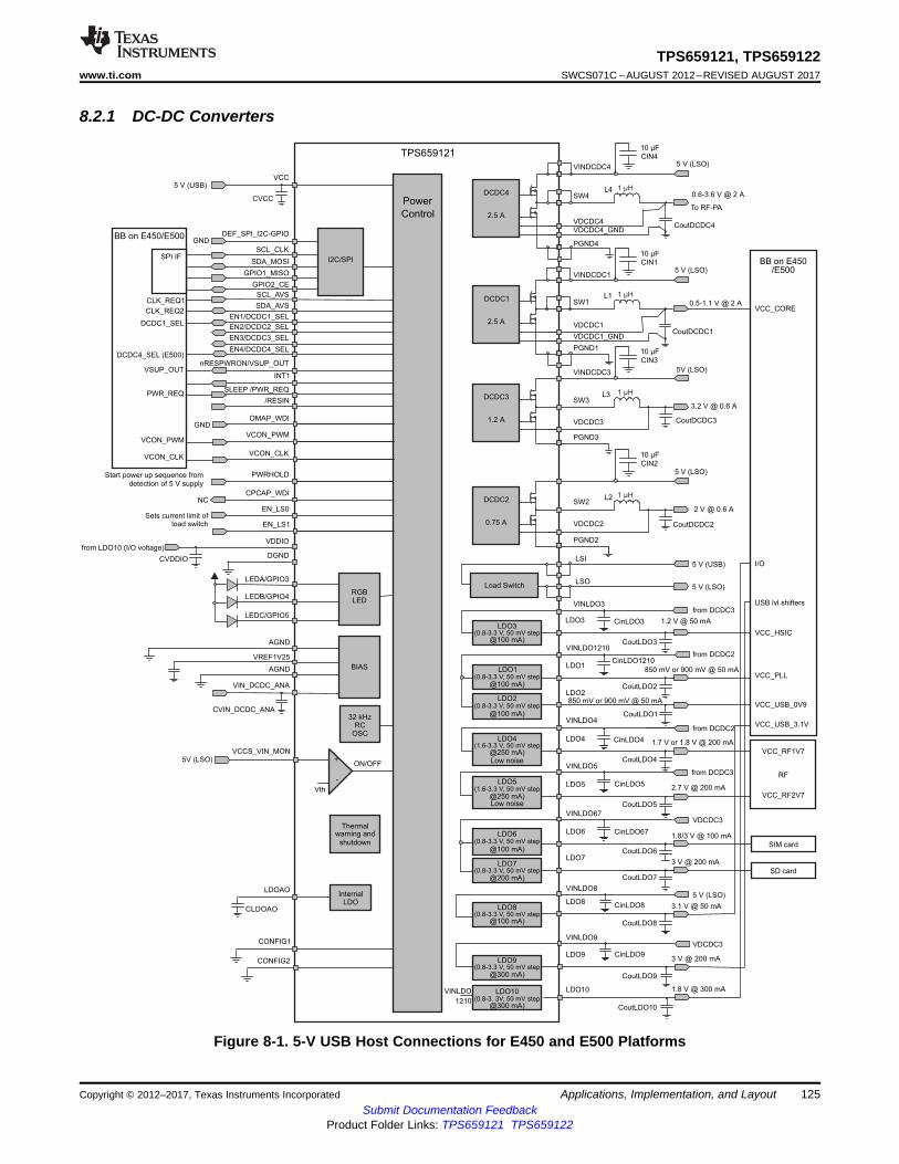
0.6-3.6 V @ 2 A
0.5-1.1 V @ 2 A
3.2 V @ 0.6 A
2 V @ 0.6 A
BB on E450/E500
VCC_CORE
VCC_PLL
VCC_USB_0V9850 mV or 900 mV @ 50 mA
I/O
To RF-PA
3.1 V @ 50 mA
RF
1.7 V or 1.8 V @ 200 mA
3 V @ 200 mA
1.2 V @ 50 mA
VCC_HSIC
1.8 V @ 300 mA
Start power up sequence from
detection of 5 V supply
VCC_USB_3.1V
1.8/3 V @ 100 mA
BB on E450/E500
SPI IF
DCDC1_SEL
CLK_REQ1
PWR_REQ
DCDC4_SEL (E500)
3 V @ 200 mA
USB lvl shifters
2.7 V @ 200 mA
VDCDC3
SDA_MOSI
SCL_CLK
VINLDO3
LDO3
VDDIO
SW4DCDC4
2.5 AVDCDC4
VINDCDC4
AGND
VREF1V25
PGND4
SW3DCDC3
1.2 A VDCDC3
PGND3
SW2DCDC2
0.75 A
PGND2
GPIO2_CE
GPIO1_MISO
I2C/SPI
/RESIN
nRESPWRON/VSUP_OUT
INT1
SLEEP /PWR_REQ
PWRHOLD
DGND
VINLDO1210
LDO1LDO1
(0.8-3.3 V, 50 mV step@100 mA)
LDO2
VINLDO4
LDO4LDO4(1.6-3.3 V, 50 mV step
@250 mA)Low noise
LDO5
LDO6
VINLDO5
LDO7
LDO8
LDO9LDO9
(0.8-3.3 V, 50 mV step@300 mA)
RGBLED
BIAS
Power
Control
TPS659121
32 kHzRC
OSC
VCCS_VIN_MON
ON/OFF
Vth
+
-
SDA_AVS
SCL_AVS
EN1/DCDC1_SEL
EN2/DCDC2_SEL
VINLDO67
LDO6(0.8-3.3 V, 50 mV step
@100 mA)
LDO3(0.8-3.3 V, 50 mV step
@100 mA)
LDO8(0.8-3.3 V, 50 mV step
@100 mA)
EN3/DCDC3_SEL
Thermalwarning and
shutdown
LDOAOInternal
LDO
LEDA/GPIO3
LEDB/GPIO4
LEDC/GPIO5
LDO10LDO10(0.8-3. 3V, 50 mV step
@300 mA)
VINLDO
1210
Load Switch
from DCDC3
LSI
LSO
L4
L3
L2
CoutDCDC4
CoutDCDC3
CoutDCDC2
VDCDC4_GND
SW1DCDC1
2.5 AVDCDC1
VINDCDC1
PGND1
L1
CoutDCDC1VDCDC1_GND
VINDCDC3
VDCDC2
CoutLDO3
CoutLDO2
CoutLDO1
CoutLDO4
CoutLDO5
CoutLDO6
CoutLDO7
CoutLDO8
CoutLDO9
CoutLDO10
CinLDO67
CinLDO5
CinLDO4
CinLDO1210
CinLDO3
VINLDO8
CinLDO8
VINLDO9
CinLDO9
VDCDC3
VCON_PWM
VCON_CLK
OMAP_WDI
CONFIG1
CONFIG2
VIN_DCDC_ANA
850 mV or 900 mV @ 50 mA
from DCDC2
5 V (USB)
5 V (LSO)
5 V (LSO)
5 V (LSO)
5V (LSO)
5 V (LSO)
VCC_RF1V7
VCC_RF2V7
from DCDC2
from DCDC3
5 V (LSO)
5V (LSO)
EN4/DCDC4_SEL
VCON_CLK
VCON_PWM
from LDO10 (I/O voltage)
CLK_REQ2
VSUP_OUT
DEF_SPI_I2C-GPIO
AGND
VCC5 V (USB)
CPCAP_WDINC
EN_LS1
EN_LS0Sets current limit of
load switch
GND
GND
CVIN_DCDC_ANA
CVCC
CLDOAO
CVDDIO
1 µH
CIN4
10 µF
CIN1
10 µF
CIN3
10 µF
CIN2
10 µF
1 µH
1 µH
1 µH
SD card
SIM card
LDO2(0.8-3.3 V, 50 mV step
@100 mA)
LDO5(1.6-3.3 V, 50 mV step
@250 mA)Low noise
LDO7(0.8-3.3 V, 50 mV step
@200 mA)
125
TPS659121, TPS659122www.ti.com SWCS071C –AUGUST 2012–REVISED AUGUST 2017
Submit Documentation FeedbackProduct Folder Links: TPS659121 TPS659122
Applications, Implementation, and LayoutCopyright © 2012–2017, Texas Instruments Incorporated
8.2.1 DC-DC Converters
Figure 8-1. 5-V USB Host Connections for E450 and E500 Platforms
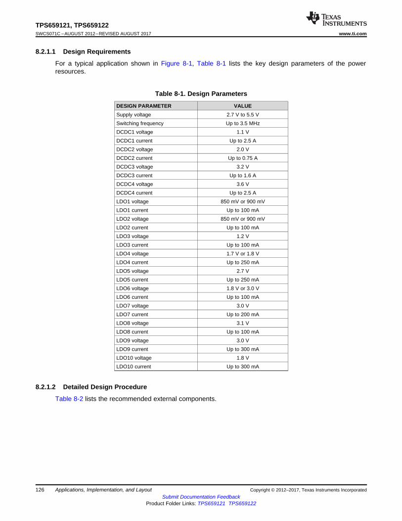
126
TPS659121, TPS659122SWCS071C –AUGUST 2012–REVISED AUGUST 2017 www.ti.com
Submit Documentation FeedbackProduct Folder Links: TPS659121 TPS659122
Applications, Implementation, and Layout Copyright © 2012–2017, Texas Instruments Incorporated
8.2.1.1 Design Requirements
For a typical application shown in Figure 8-1, Table 8-1 lists the key design parameters of the powerresources.
Table 8-1. Design Parameters
DESIGN PARAMETER VALUESupply voltage 2.7 V to 5.5 VSwitching frequency Up to 3.5 MHzDCDC1 voltage 1.1 VDCDC1 current Up to 2.5 ADCDC2 voltage 2.0 VDCDC2 current Up to 0.75 ADCDC3 voltage 3.2 VDCDC3 current Up to 1.6 ADCDC4 voltage 3.6 VDCDC4 current Up to 2.5 ALDO1 voltage 850 mV or 900 mVLDO1 current Up to 100 mALDO2 voltage 850 mV or 900 mVLDO2 current Up to 100 mALDO3 voltage 1.2 VLDO3 current Up to 100 mALDO4 voltage 1.7 V or 1.8 VLDO4 current Up to 250 mALDO5 voltage 2.7 VLDO5 current Up to 250 mALDO6 voltage 1.8 V or 3.0 VLDO6 current Up to 100 mALDO7 voltage 3.0 VLDO7 current Up to 200 mALDO8 voltage 3.1 VLDO8 current Up to 100 mALDO9 voltage 3.0 VLDO9 current Up to 300 mALDO10 voltage 1.8 VLDO10 current Up to 300 mA
8.2.1.2 Detailed Design Procedure
Table 8-2 lists the recommended external components.
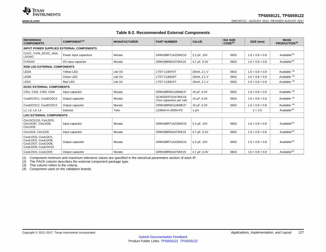
Copyright © 2012–2017, Texas Instruments Incorporated Applications, Implementation, and LayoutSubmit Documentation Feedback
Product Folder Links: TPS659121 TPS659122
127
TPS659121, TPS659122www.ti.com SWCS071C –AUGUST 2012–REVISED AUGUST 2017
(1) Component minimum and maximum tolerance values are specified in the electrical parameters section of each IP.(2) The PACK column describes the external component package type.(3) This column refers to the criteria.(4) Component used on the validation boards.
Table 8-2. Recommended External ComponentsREFERENCECOMPONENTS COMPONENT (1) MANUFACTURER PART NUMBER VALUE EIA SIZE
CODE (2) SIZE (mm) MASSPRODUCTION (3)
INPUT POWER SUPPLIES EXTERNAL COMPONENTS
CVCC, CVIN_DCDC_ANA,LDOAO Power input capacitors Murata GRM188R71A225KE15 2.2 µF, 10V 0603 1.6 × 0.8 × 0.8 Available (4)
CVDDIO I/O input capacitor Murata GRM188R60J475KE19 4.7 µF, 6.3V 0603 1.6 × 0.8 × 0.8 Available (4)
RGB LED EXTERNAL COMPONENTS
LEDA Yellow LED Lite On LTST-C190YKT 20mA, 2.1 V 0603 1.6 × 0.8 × 0.8 Available (4)
LEDB Green LED Lite On LTST-C190GKT 20mA, 2.1 V 0603 1.6 × 0.8 × 0.8 Available (4)
LEDC Red LED Lite On LTST-C190CKT 20mA, 2.1 V 0603 1.6 × 0.8 × 0.8 Available (4)
DCDC EXTERNAL COMPONENTS
CIN1, CIN2, CIN3, CIN4 Input capacitor Murata GRM188R60J106ME47 10 µF, 6.3V 0603 1.6 × 0.8 × 0.8 Available (4)
CoutDCDC1, CoutDCDC4 Output capacitor Murata GCM32ER70J476KE19(Two capacitors per rail) 10 µF, 6.3V 0603 1.6 × 0.8 × 0.8 Available (4)
CoutDCDC2, CoutDCDC3 Output capacitor Murata GRM188R60J106ME47 10 µF, 6.3V 0603 1.6 × 0.8 × 0.8 Available (4)
L1, L2, L3, L4 Inductor Toko 1239AS-H-1R0N=P2 1 µH 2 × 2.5 Available (4)
LDO EXTERNAL COMPONENTS
CinLDO1210, CinLDO3,CinLDO67, CinLDO8,CinLDO9
Input capacitor Murata GRM188R71A225KE15 2.2 µF, 10V 0603 1.6 × 0.8 × 0.8 Available (4)
CinLDO4, CinLDO5 Input capacitor Murata GRM188R60J475KE19 4.7 µF, 6.3V 0603 1.6 × 0.8 × 0.8 Available (4)
CoutLDO3, CoutLDO1,CoutLDO2, CoutLDO6,CoutLDO7, CoutLDO8,CoutLDO9, CoutLDO10
Output capacitor Murata GRM188R71A225KE15 2.2 µF, 10V 0603 1.6 × 0.8 × 0.8 Available (4)
CoutLDO4, CoutLDO5 Output capacitor Murata GRM188R60J475KE19 4.7 µF, 6.3V 0603 1.6 × 0.8 × 0.8 Available (4)
LLmax outmax
II = I +
2
D
L
Vout1
VinI = Vout
L
-
D ´´ ¦
128
TPS659121, TPS659122SWCS071C –AUGUST 2012–REVISED AUGUST 2017 www.ti.com
Submit Documentation FeedbackProduct Folder Links: TPS659121 TPS659122
Applications, Implementation, and Layout Copyright © 2012–2017, Texas Instruments Incorporated
8.2.1.2.1 Output Filter Design (Inductor and Output Capacitor)
8.2.1.2.1.1 Inductor Selection
The step-down converters are designed to operate with small external components such as 1-μH outputinductors. The values given under the recommended operating conditions include tolerances andsaturation effects and must not be violated for stable operation. The selected inductor must be rated for itsDC resistance and saturation current. The DC resistance of the inductance will influence directly theefficiency of the converter. Therefore an inductor with lowest DC resistance should be selected for highestefficiency.
Equation 2 can be used to calculate the maximum inductor current under static load conditions. Thesaturation current of the inductor should be rated higher than the maximum inductor current as calculatedwith Equation 2. This is recommended because during heavy load transient the inductor current will riseabove the calculated value.
where• ΔIL = Peak-to-peak inductor ripple current• L = Inductor value• f = Switching frequency (2)
where• ILmax = Maximum inductor current (3)
The highest inductor current will occur at maximum Vin.
Open core inductors have a soft saturation characteristic and they can usually handle higher inductorcurrents versus a comparable shielded inductor.
A more conservative approach is to select the inductor current rating just for the maximum switch currentof the corresponding converter. It must be considered, that the core material from inductor to inductordiffers and will have an impact on the efficiency especially at high switching frequencies.
Refer to Table 8-3 and the typical applications for possible inductors.
Table 8-3. Tested Inductors
INDUCTOR TYPE NOMINAL INDUCTANCE SUPPLIERDFE252012 1 μH TokoDFE322510 1 μH TokoDFE322512 1 μH Toko
VLS201612ET-1R0 1 μH TDKSPM3012T-1R0 1 μH TDK
8.2.1.2.1.2 Output Capacitor Selection
The control scheme of the DC-DC converters allow the use of small ceramic capacitors with a typicalvalue as given in the recommended operating conditions, without having large output voltage under andovershoots during heavy load transients. Ceramic capacitors having low ESR values result in lowestoutput voltage ripple and are therefore recommended.
Vout1
1VinVout = Vout + ESR
L 8 Cout
- æ öD ´ ´ ç ÷´ ¦ ´ ´ ¦è ø
RMSCout
Vout1
1VinI = Vout
L 2 3
-
´ ´´ ¦ ´
129
TPS659121, TPS659122www.ti.com SWCS071C –AUGUST 2012–REVISED AUGUST 2017
Submit Documentation FeedbackProduct Folder Links: TPS659121 TPS659122
Applications, Implementation, and LayoutCopyright © 2012–2017, Texas Instruments Incorporated
If ceramic output capacitors are used, the capacitor RMS ripple current rating will always meet theapplication requirements. Just for completeness the RMS ripple current is calculated as shown inEquation 4.
(4)
At nominal load current, the inductive converters operate in PWM mode and the overall output-voltageripple is the sum of the voltage spike caused by the output capacitor ESR plus the voltage ripple causedby charging and discharging the output capacitor. See Equation 5.
(5)
Where the highest output voltage ripple occurs at the highest input voltage, Vin.
At light load currents, the converters operate in Power Save Mode and the output voltage ripple isdependent on the value of the output capacitor. The output voltage ripple is set by the internal comparatordelay and the external capacitor. The typical output voltage ripple is less than 1% of the nominal outputvoltage.
8.2.1.2.1.3 Input Capacitor Selection / Input Voltage
Because of the nature of the buck converter having a pulsating input current, a low ESR input capacitor isrequired for best input voltage filtering and minimizing the interference with other circuits caused by highinput-voltage spikes. The converters need a ceramic input capacitor of 10 μF. The input capacitor can beincreased without any limit for better input voltage filtering. Ceramic capacitors suffer from the so-called dcbias effect. A dc voltage applied at a ceramic capacitor will change the effective capacitance to a valuelower than the nominal value. Curves about that behavior are available at the capacitor manufacturers andneed to be considered when using the capacitors in applications where a dc voltage is applied and aminimum capacitance must be maintained for proper functionality of the circuit. The values given in theRecommended operating Conditions for TPS65912x are for the capacitance. The actual capacitor usedmay have a larger nominal value that drops with the voltage applied to what is recommended. Thecapacitance drop depends on the voltage applied, so for a higher voltage; for example, the output voltageof a DC-DC converter or LDO, this must be considered when choosing a proper capacitor.
The input voltage for the step-down converters must be connected to pin VINDCDC1, VINDCDC2,VINDCDC3 and VINDCDC4. These pins need to be tied together with VIN_DCDC_ANA to the powersource. VCC must be tied to the highest voltage in the system. If the load switch is used as switch on theoutput, VCC must be tied to the input voltage of VINDCDx and VIN_DCDC_ANA. If the load switch isused as a current limited switch on the input, VCC must be connected to pin LSI while LSO is connectedto VINDCDCx and VINDCDC_ANA. The four step-down converters must not be supplied from differentinput voltages.
8.2.1.2.1.4 Output Capacitor Table
The DC-DC converters are designed for an output capacitance as listed under the RecommendedOperating Conditions. A ceramic capacitor, such as X5R or X7R type, is required at the output. Table 8-4lists capacitors used for TPS65912x.
Table 8-4. Possible Capacitors
Value Size Vendor Material and Rating47 µF / 6.3 V 0805 Murata GRM21BR60J476ME15 Ceramic X5R22 µF / 6.3 V 0805 Murata GRM21BR60J226M Ceramic X5R10 µF / 10 V 0603 Murata GRM188R61A106ME69 Ceramic X5R
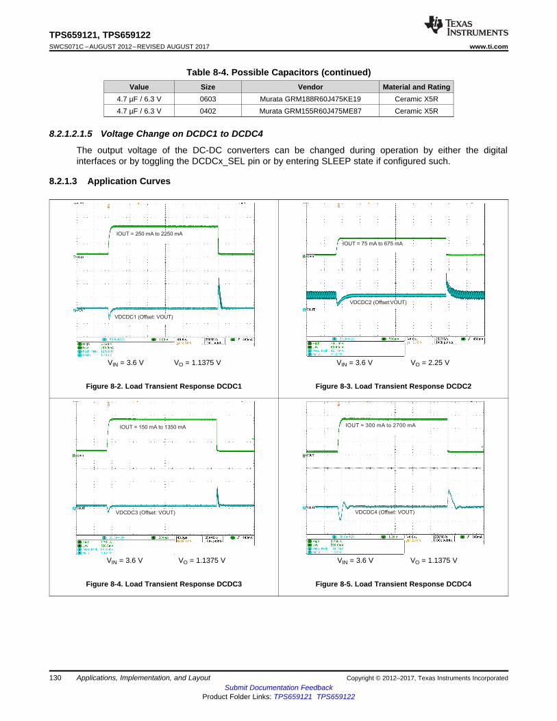
IOUT = 150 mA to 1350 mA
VDCDC3 (Offset: VOUT) VDCDC4 (Offset: VOUT)
IOUT = 300 mA to 2700 mA
VDCDC1 (Offset: VOUT)
IOUT = 250 mA to 2250 mA
VDCDC2 (Offset:VOUT)
IOUT = 75 mA to 675 mA
130
TPS659121, TPS659122SWCS071C –AUGUST 2012–REVISED AUGUST 2017 www.ti.com
Submit Documentation FeedbackProduct Folder Links: TPS659121 TPS659122
Applications, Implementation, and Layout Copyright © 2012–2017, Texas Instruments Incorporated
Table 8-4. Possible Capacitors (continued)Value Size Vendor Material and Rating
4.7 µF / 6.3 V 0603 Murata GRM188R60J475KE19 Ceramic X5R4.7 µF / 6.3 V 0402 Murata GRM155R60J475ME87 Ceramic X5R
8.2.1.2.1.5 Voltage Change on DCDC1 to DCDC4
The output voltage of the DC-DC converters can be changed during operation by either the digitalinterfaces or by toggling the DCDCx_SEL pin or by entering SLEEP state if configured such.
8.2.1.3 Application Curves
VIN = 3.6 V VO = 1.1375 V
Figure 8-2. Load Transient Response DCDC1
VIN = 3.6 V VO = 2.25 V
Figure 8-3. Load Transient Response DCDC2
VIN = 3.6 V VO = 1.1375 V
Figure 8-4. Load Transient Response DCDC3
VIN = 3.6 V VO = 1.1375 V
Figure 8-5. Load Transient Response DCDC4
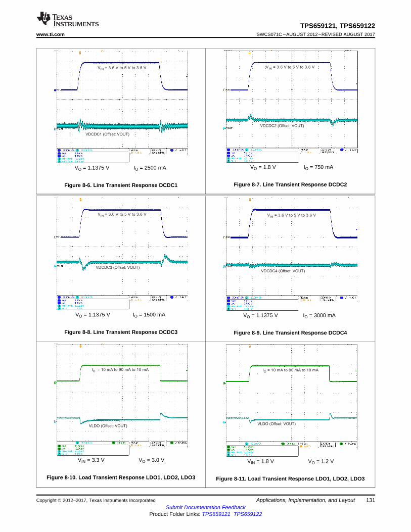
I = 10 mA to 90 mA to 10 mAO
VLDO (Offset: VOUT)VLDO (Offset: VOUT)
I = 10 mA to 90 mA to 10 mAO
VDCDC4 (Offset: VOUT)
VIN = 3.6 V to 5 V to 3.6 V
VDCDC3 (Offset: VOUT)
V = 3.6 V to 5 V to 3.6 VIN
VDCDC1 (Offset: VOUT)
V = 3.6 V to 5 V to 3.6 VIN
VDCDC2 (Offset: VOUT)
V = 3.6 V to 5 V to 3.6 VIN
131
TPS659121, TPS659122www.ti.com SWCS071C –AUGUST 2012–REVISED AUGUST 2017
Submit Documentation FeedbackProduct Folder Links: TPS659121 TPS659122
Applications, Implementation, and LayoutCopyright © 2012–2017, Texas Instruments Incorporated
VO = 1.1375 V IO = 2500 mA
Figure 8-6. Line Transient Response DCDC1
VO = 1.8 V IO = 750 mA
Figure 8-7. Line Transient Response DCDC2
VO = 1.1375 V IO = 1500 mA
Figure 8-8. Line Transient Response DCDC3
VO = 1.1375 V IO = 3000 mA
Figure 8-9. Line Transient Response DCDC4
VIN = 3.3 V VO = 3.0 V
Figure 8-10. Load Transient Response LDO1, LDO2, LDO3
VIN = 1.8 V VO = 1.2 V
Figure 8-11. Load Transient Response LDO1, LDO2, LDO3
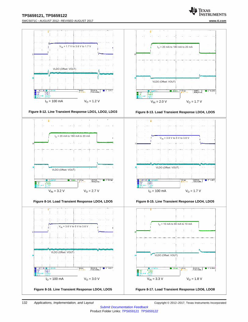
VLDO (Offset: VOUT)
V = 3.6 V to 5 V to 3.6 VIN
VLDO (Offset: VOUT)
I = 10 mA to 90 mA to 10 mAO
I = 20 mA to 180 mA to 20 mAO
VLDO (Offset: VOUT)
V = 3.6 V to 5 V to 3.6 VIN
VLDO (Offset: VOUT)
VLDO (Offset: VOUT)
I = 20 mA to 180 mA to 20 mAO
VLDO (Offset: VOUT)
V = 1.7 V to 3.6 V to 1.7 VIN
132
TPS659121, TPS659122SWCS071C –AUGUST 2012–REVISED AUGUST 2017 www.ti.com
Submit Documentation FeedbackProduct Folder Links: TPS659121 TPS659122
Applications, Implementation, and Layout Copyright © 2012–2017, Texas Instruments Incorporated
IO = 100 mA VO = 1.2 V
Figure 8-12. Line Transient Response LDO1, LDO2, LDO3
VIN = 2.0 V VO = 1.7 V
Figure 8-13. Load Transient Response LDO4, LDO5
VIN = 3.2 V VO = 2.7 V
Figure 8-14. Load Transient Response LDO4, LDO5
IO = 100 mA VO = 1.7 V
Figure 8-15. Line Transient Response LDO4, LDO5
IO = 100 mA VO = 3.0 V
Figure 8-16. Line Transient Response LDO4, LDO5
VIN = 3.3 V VO = 1.8 V
Figure 8-17. Load Transient Response LDO6, LDO8
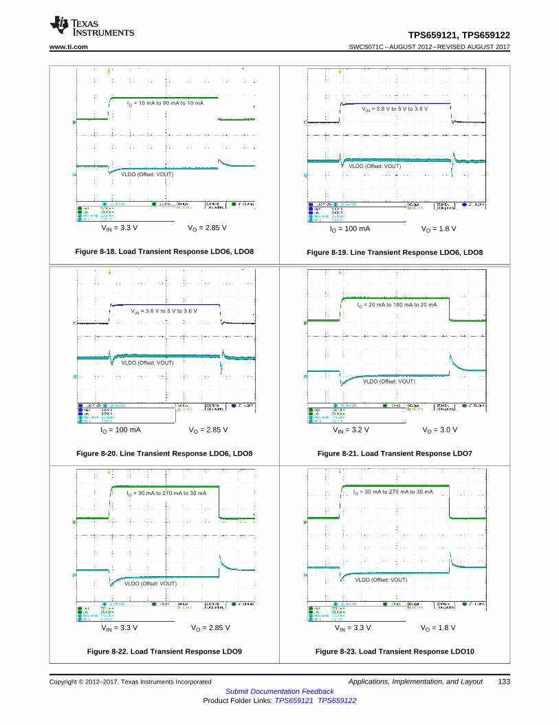
I = 30 mA to 270 mA to 30 mAO
VLDO (Offset: VOUT)VLDO (Offset: VOUT)
I = 30 mA to 270 mA to 30 mAO
VLDO (Offset: VOUT)
V = 3.6 V to 5 V to 3.6 VIN
VLDO (Offset: VOUT)
I = 20 mA to 180 mA to 20 mAO
V = 3.6 V to 5 V to 3.6 VIN
VLDO (Offset: VOUT)
I = 10 mA to 90 mA to 10 mAO
VLDO (Offset: VOUT)
133
TPS659121, TPS659122www.ti.com SWCS071C –AUGUST 2012–REVISED AUGUST 2017
Submit Documentation FeedbackProduct Folder Links: TPS659121 TPS659122
Applications, Implementation, and LayoutCopyright © 2012–2017, Texas Instruments Incorporated
VIN = 3.3 V VO = 2.85 V
Figure 8-18. Load Transient Response LDO6, LDO8
IO = 100 mA VO = 1.8 V
Figure 8-19. Line Transient Response LDO6, LDO8
IO = 100 mA VO = 2.85 V
Figure 8-20. Line Transient Response LDO6, LDO8
VIN = 3.2 V VO = 3.0 V
Figure 8-21. Load Transient Response LDO7
VIN = 3.3 V VO = 2.85 V
Figure 8-22. Load Transient Response LDO9
VIN = 3.3 V VO = 1.8 V
Figure 8-23. Load Transient Response LDO10
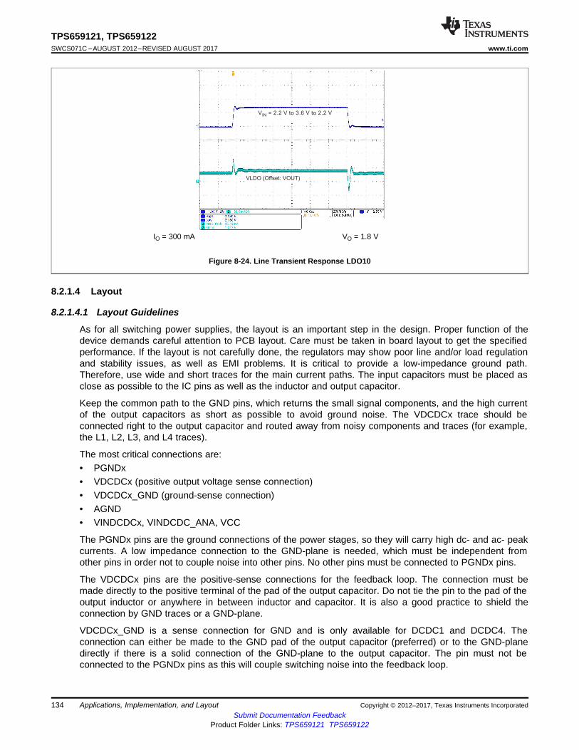
VLDO (Offset: VOUT)
V = 2.2 V to 3.6 V to 2.2 VIN
134
TPS659121, TPS659122SWCS071C –AUGUST 2012–REVISED AUGUST 2017 www.ti.com
Submit Documentation FeedbackProduct Folder Links: TPS659121 TPS659122
Applications, Implementation, and Layout Copyright © 2012–2017, Texas Instruments Incorporated
IO = 300 mA VO = 1.8 V
Figure 8-24. Line Transient Response LDO10
8.2.1.4 Layout
8.2.1.4.1 Layout Guidelines
As for all switching power supplies, the layout is an important step in the design. Proper function of thedevice demands careful attention to PCB layout. Care must be taken in board layout to get the specifiedperformance. If the layout is not carefully done, the regulators may show poor line and/or load regulationand stability issues, as well as EMI problems. It is critical to provide a low-impedance ground path.Therefore, use wide and short traces for the main current paths. The input capacitors must be placed asclose as possible to the IC pins as well as the inductor and output capacitor.
Keep the common path to the GND pins, which returns the small signal components, and the high currentof the output capacitors as short as possible to avoid ground noise. The VDCDCx trace should beconnected right to the output capacitor and routed away from noisy components and traces (for example,the L1, L2, L3, and L4 traces).
The most critical connections are:• PGNDx• VDCDCx (positive output voltage sense connection)• VDCDCx_GND (ground-sense connection)• AGND• VINDCDCx, VINDCDC_ANA, VCC
The PGNDx pins are the ground connections of the power stages, so they will carry high dc- and ac- peakcurrents. A low impedance connection to the GND-plane is needed, which must be independent fromother pins in order not to couple noise into other pins. No other pins must be connected to PGNDx pins.
The VDCDCx pins are the positive-sense connections for the feedback loop. The connection must bemade directly to the positive terminal of the pad of the output capacitor. Do not tie the pin to the pad of theoutput inductor or anywhere in between inductor and capacitor. It is also a good practice to shield theconnection by GND traces or a GND-plane.
VDCDCx_GND is a sense connection for GND and is only available for DCDC1 and DCDC4. Theconnection can either be made to the GND pad of the output capacitor (preferred) or to the GND-planedirectly if there is a solid connection of the GND-plane to the output capacitor. The pin must not beconnected to the PGNDx pins as this will couple switching noise into the feedback loop.
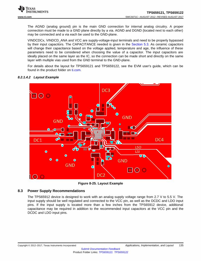
135
TPS659121, TPS659122www.ti.com SWCS071C –AUGUST 2012–REVISED AUGUST 2017
Submit Documentation FeedbackProduct Folder Links: TPS659121 TPS659122
Applications, Implementation, and LayoutCopyright © 2012–2017, Texas Instruments Incorporated
The AGND (analog ground) pin is the main GND connection for internal analog circuitry. A properconnection must be made to a GND plane directly by a via. AGND and DGND (located next to each other)may be connected and a via each be used to the GND-plane.
VINDCDCx, VINDCD_ANA and VCC are supply-voltage-input terminals and need to be properly bypassedby their input capacitors. The CAPACITANCE needed is given in the Section 5.3. As ceramic capacitorswill change their capacitance based on the voltage applied, temperature and age, the influence of theseparameters need to be considered when choosing the value of a capacitor. The input capacitors areideally placed on the same layer as the IC, so the connection can be made short and directly on the samelayer with multiple vias used from the GND terminal to the GND-plane.
For details about the layout for TPS659121 and TPS659122, see the EVM user's guide, which can befound in the product folder on ti.com.
8.2.1.4.2 Layout Example
Figure 8-25. Layout Example
8.3 Power Supply RecommendationsThe TPS65912 device is designed to work with an analog supply voltage range from 2.7 V to 5.5 V. Theinput supply should be well regulated and connected to the VCC pin, as well as the DCDC and LDO inputpins. If the input supply is located more than a few inches from the TPS65912 device, additionalcapacitance may be required in addition to the recommended input capacitors at the VCC pin and theDCDC and LDO input pins.
136
TPS659121, TPS659122SWCS071C –AUGUST 2012–REVISED AUGUST 2017 www.ti.com
Submit Documentation FeedbackProduct Folder Links: TPS659121 TPS659122
Device and Documentation Support Copyright © 2012–2017, Texas Instruments Incorporated
9 Device and Documentation Support
9.1 Device Support
9.1.1 Development SupportTI offers an extensive line of development tools, including tools to evaluate the performance of theprocessors, generate code, develop algorithm implementations, and fully integrate and debug softwareand hardware modules. The tool's support documentation is electronically available within the CodeComposer Studio™ Integrated Development Environment (IDE).
The following products support development of the TPS659121 and TPS659122 device applications:
Software Development Tools: Code Composer Studio™ Integrated Development Environment (IDE):including Editor C/C++/Assembly Code Generation, and Debug plus additional development toolsScalable, Real-Time Foundation Software ( DSP/BIOS™), which provides the basic run-time targetsoftware needed to support any TPS659121 and TPS659122 device application.
Hardware Development Tools: Extended Development System ( XDS™) Emulator
For a complete listing of development-support tools for the TPS659121 and TPS659122 platform, visit theTexas Instruments website at www.ti.com. For information on pricing and availability, contact the nearestTI field sales office or authorized distributor.
9.1.2 Device NomenclatureTo designate the stages in the product development cycle, TI assigns prefixes to the part numbers of allmicroprocessors (MPUs) and support tools. Each device has one of three prefixes: X, P, or null (no prefix)(for example, TPS659121 and TPS659122).
Device development evolutionary flow:X Experimental device that is not necessarily representative of the final device's electrical
specifications and may not use production assembly flow.P Prototype device that is not necessarily the final silicon die and may not necessarily meet
final electrical specifications.null Production version of the silicon die that is fully qualified.
X and P devices are shipped against the following disclaimer:
"Developmental product is intended for internal evaluation purposes."
Production devices have been characterized fully, and the quality and reliability of the device have beendemonstrated fully. TI's standard warranty applies.
Predictions show that prototype devices (X or P) have a greater failure rate than the standard productiondevices. Texas Instruments recommends that these devices not be used in any production systembecause their expected end-use failure rate still is undefined. Only qualified production devices are to beused.
For orderable part numbers of TPS659121 and TPS659122 devices in the YFF package types, see thePackage Option Addendum of this document, the TI website (www.ti.com), or contact your TI salesrepresentative.
9.2 Documentation Support
9.2.1 Related DocumentationFor related documentation see the following:Texas Instruments, TPS65912xEVM-081 User's Guide
9.3 Receiving Notification of Documentation Updates
137
TPS659121, TPS659122www.ti.com SWCS071C –AUGUST 2012–REVISED AUGUST 2017
Submit Documentation FeedbackProduct Folder Links: TPS659121 TPS659122
Mechanical, Packaging, and Orderable InformationCopyright © 2012–2017, Texas Instruments Incorporated
To receive notification of documentation updates, navigate to the device product folder on ti.com. In theupper right corner, click on Alert me to register and receive a weekly digest of any product information thathas changed. For change details, review the revision history included in any revised document.
9.4 Community ResourcesThe following links connect to TI community resources. Linked contents are provided "AS IS" by therespective contributors. They do not constitute TI specifications and do not necessarily reflect TI's views;see TI's Terms of Use.TI E2E™ Online Community The TI engineer-to-engineer (E2E) community was created to foster
collaboration among engineers. At e2e.ti.com, you can ask questions, share knowledge,explore ideas and help solve problems with fellow engineers.
Design Support TI's Design Support Quickly find helpful E2E forums along with design support toolsand contact information for technical support.
9.5 TrademarksEco-mode, Code Composer Studio, DSP/BIOS, XDS, E2E are trademarks of Texas Instruments.NXP is a registered trademark of NXP Semiconductors.All other trademarks are the property of their respective owners.
9.6 Electrostatic Discharge CautionThis integrated circuit can be damaged by ESD. Texas Instruments recommends that all integrated circuits be handled withappropriate precautions. Failure to observe proper handling and installation procedures can cause damage.
ESD damage can range from subtle performance degradation to complete device failure. Precision integrated circuits may be moresusceptible to damage because very small parametric changes could cause the device not to meet its published specifications.
9.7 GlossaryTI Glossary This glossary lists and explains terms, acronyms, and definitions.
10 Mechanical, Packaging, and Orderable Information
The following pages include mechanical, packaging, and orderable information. This information is themost current data available for the designated devices. This data is subject to change without notice andrevision of this document. For browser-based versions of this data sheet, refer to the left-hand navigation.
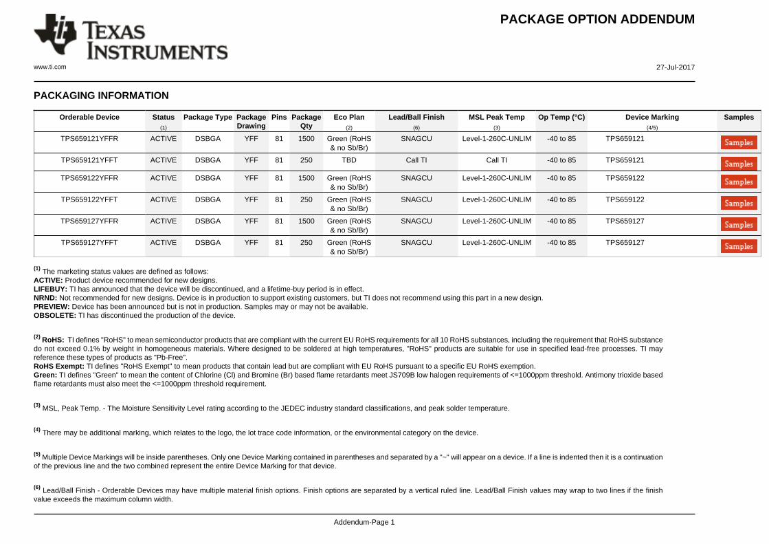
PACKAGE OPTION ADDENDUM
www.ti.com 27-Jul-2017
Addendum-Page 1
PACKAGING INFORMATION
Orderable Device Status(1)
Package Type PackageDrawing
Pins PackageQty
Eco Plan(2)
Lead/Ball Finish(6)
MSL Peak Temp(3)
Op Temp (°C) Device Marking(4/5)
Samples
TPS659121YFFR ACTIVE DSBGA YFF 81 1500 Green (RoHS& no Sb/Br)
SNAGCU Level-1-260C-UNLIM -40 to 85 TPS659121
TPS659121YFFT ACTIVE DSBGA YFF 81 250 TBD Call TI Call TI -40 to 85 TPS659121
TPS659122YFFR ACTIVE DSBGA YFF 81 1500 Green (RoHS& no Sb/Br)
SNAGCU Level-1-260C-UNLIM -40 to 85 TPS659122
TPS659122YFFT ACTIVE DSBGA YFF 81 250 Green (RoHS& no Sb/Br)
SNAGCU Level-1-260C-UNLIM -40 to 85 TPS659122
TPS659127YFFR ACTIVE DSBGA YFF 81 1500 Green (RoHS& no Sb/Br)
SNAGCU Level-1-260C-UNLIM -40 to 85 TPS659127
TPS659127YFFT ACTIVE DSBGA YFF 81 250 Green (RoHS& no Sb/Br)
SNAGCU Level-1-260C-UNLIM -40 to 85 TPS659127
(1) The marketing status values are defined as follows:ACTIVE: Product device recommended for new designs.LIFEBUY: TI has announced that the device will be discontinued, and a lifetime-buy period is in effect.NRND: Not recommended for new designs. Device is in production to support existing customers, but TI does not recommend using this part in a new design.PREVIEW: Device has been announced but is not in production. Samples may or may not be available.OBSOLETE: TI has discontinued the production of the device.
(2) RoHS: TI defines "RoHS" to mean semiconductor products that are compliant with the current EU RoHS requirements for all 10 RoHS substances, including the requirement that RoHS substancedo not exceed 0.1% by weight in homogeneous materials. Where designed to be soldered at high temperatures, "RoHS" products are suitable for use in specified lead-free processes. TI mayreference these types of products as "Pb-Free".RoHS Exempt: TI defines "RoHS Exempt" to mean products that contain lead but are compliant with EU RoHS pursuant to a specific EU RoHS exemption.Green: TI defines "Green" to mean the content of Chlorine (Cl) and Bromine (Br) based flame retardants meet JS709B low halogen requirements of <=1000ppm threshold. Antimony trioxide basedflame retardants must also meet the <=1000ppm threshold requirement.
(3) MSL, Peak Temp. - The Moisture Sensitivity Level rating according to the JEDEC industry standard classifications, and peak solder temperature.
(4) There may be additional marking, which relates to the logo, the lot trace code information, or the environmental category on the device.
(5) Multiple Device Markings will be inside parentheses. Only one Device Marking contained in parentheses and separated by a "~" will appear on a device. If a line is indented then it is a continuationof the previous line and the two combined represent the entire Device Marking for that device.
(6) Lead/Ball Finish - Orderable Devices may have multiple material finish options. Finish options are separated by a vertical ruled line. Lead/Ball Finish values may wrap to two lines if the finishvalue exceeds the maximum column width.
PACKAGE OPTION ADDENDUM
www.ti.com 27-Jul-2017
Addendum-Page 2
Important Information and Disclaimer:The information provided on this page represents TI's knowledge and belief as of the date that it is provided. TI bases its knowledge and belief on informationprovided by third parties, and makes no representation or warranty as to the accuracy of such information. Efforts are underway to better integrate information from third parties. TI has taken andcontinues to take reasonable steps to provide representative and accurate information but may not have conducted destructive testing or chemical analysis on incoming materials and chemicals.TI and TI suppliers consider certain information to be proprietary, and thus CAS numbers and other limited information may not be available for release.
In no event shall TI's liability arising out of such information exceed the total purchase price of the TI part(s) at issue in this document sold by TI to Customer on an annual basis.
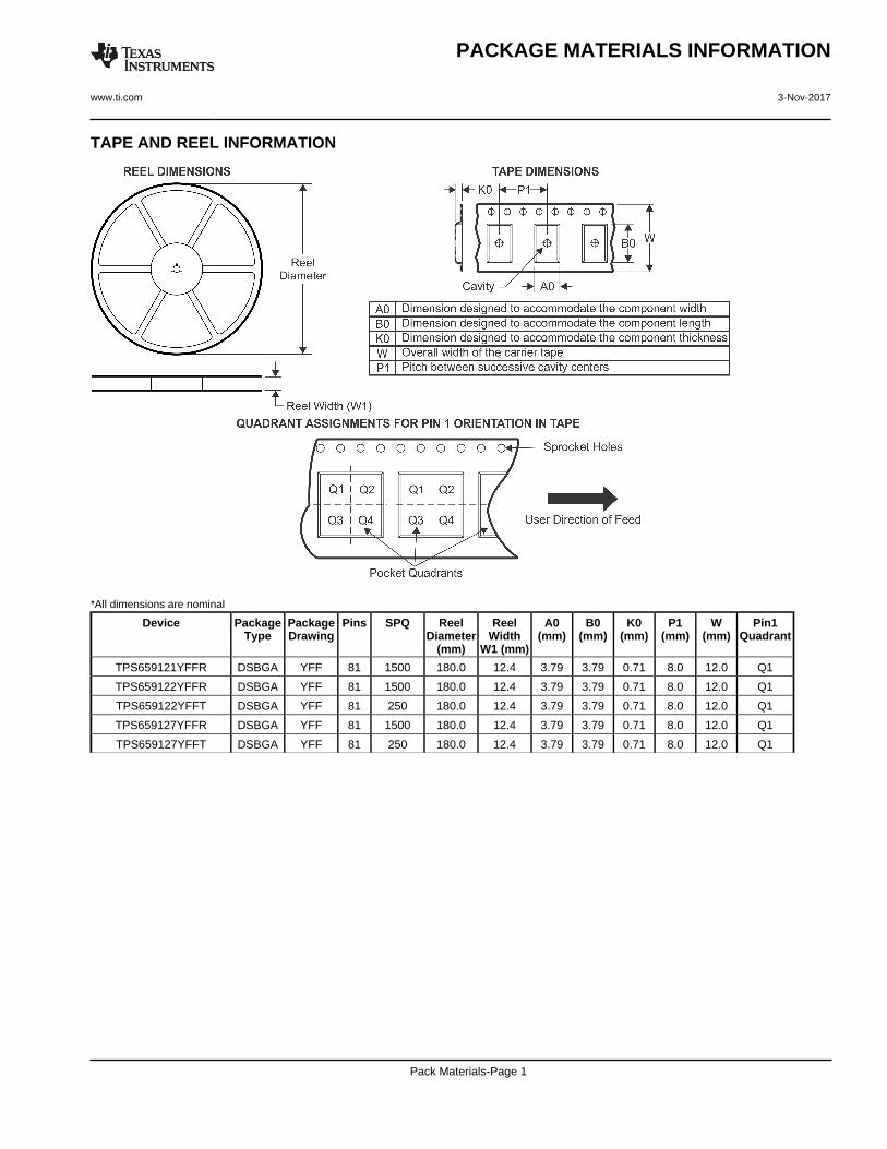
TAPE AND REEL INFORMATION
*All dimensions are nominal
Device PackageType
PackageDrawing
Pins SPQ ReelDiameter
(mm)
ReelWidth
W1 (mm)
A0(mm)
B0(mm)
K0(mm)
P1(mm)
W(mm)
Pin1Quadrant
TPS659121YFFR DSBGA YFF 81 1500 180.0 12.4 3.79 3.79 0.71 8.0 12.0 Q1
TPS659122YFFR DSBGA YFF 81 1500 180.0 12.4 3.79 3.79 0.71 8.0 12.0 Q1
TPS659122YFFT DSBGA YFF 81 250 180.0 12.4 3.79 3.79 0.71 8.0 12.0 Q1
TPS659127YFFR DSBGA YFF 81 1500 180.0 12.4 3.79 3.79 0.71 8.0 12.0 Q1
TPS659127YFFT DSBGA YFF 81 250 180.0 12.4 3.79 3.79 0.71 8.0 12.0 Q1
PACKAGE MATERIALS INFORMATION
www.ti.com 3-Nov-2017
Pack Materials-Page 1
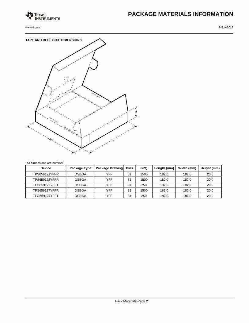
*All dimensions are nominal
Device Package Type Package Drawing Pins SPQ Length (mm) Width (mm) Height (mm)
TPS659121YFFR DSBGA YFF 81 1500 182.0 182.0 20.0
TPS659122YFFR DSBGA YFF 81 1500 182.0 182.0 20.0
TPS659122YFFT DSBGA YFF 81 250 182.0 182.0 20.0
TPS659127YFFR DSBGA YFF 81 1500 182.0 182.0 20.0
TPS659127YFFT DSBGA YFF 81 250 182.0 182.0 20.0
PACKAGE MATERIALS INFORMATION
www.ti.com 3-Nov-2017
Pack Materials-Page 2
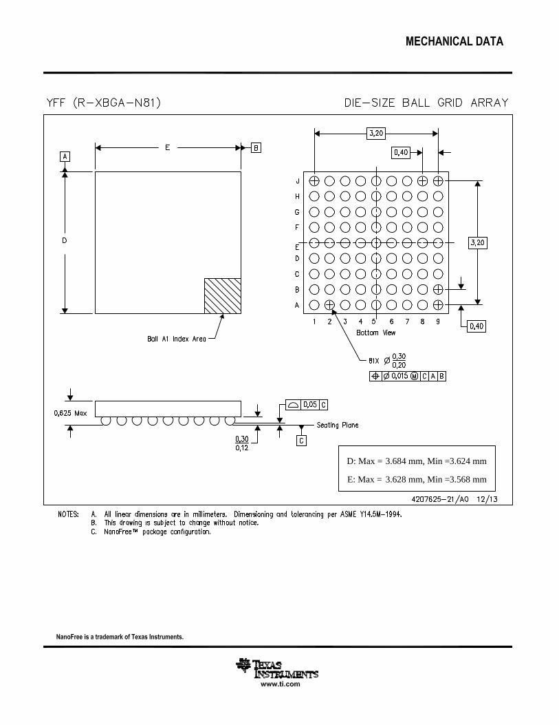
D: Max =
E: Max =
3.684 mm, Min =
3.628 mm, Min =
3.624 mm
3.568 mm
IMPORTANT NOTICE
Texas Instruments Incorporated (TI) reserves the right to make corrections, enhancements, improvements and other changes to itssemiconductor products and services per JESD46, latest issue, and to discontinue any product or service per JESD48, latest issue. Buyersshould obtain the latest relevant information before placing orders and should verify that such information is current and complete.TI’s published terms of sale for semiconductor products (http://www.ti.com/sc/docs/stdterms.htm) apply to the sale of packaged integratedcircuit products that TI has qualified and released to market. Additional terms may apply to the use or sale of other types of TI products andservices.Reproduction of significant portions of TI information in TI data sheets is permissible only if reproduction is without alteration and isaccompanied by all associated warranties, conditions, limitations, and notices. TI is not responsible or liable for such reproduceddocumentation. Information of third parties may be subject to additional restrictions. Resale of TI products or services with statementsdifferent from or beyond the parameters stated by TI for that product or service voids all express and any implied warranties for theassociated TI product or service and is an unfair and deceptive business practice. TI is not responsible or liable for any such statements.Buyers and others who are developing systems that incorporate TI products (collectively, “Designers”) understand and agree that Designersremain responsible for using their independent analysis, evaluation and judgment in designing their applications and that Designers havefull and exclusive responsibility to assure the safety of Designers' applications and compliance of their applications (and of all TI productsused in or for Designers’ applications) with all applicable regulations, laws and other applicable requirements. Designer represents that, withrespect to their applications, Designer has all the necessary expertise to create and implement safeguards that (1) anticipate dangerousconsequences of failures, (2) monitor failures and their consequences, and (3) lessen the likelihood of failures that might cause harm andtake appropriate actions. Designer agrees that prior to using or distributing any applications that include TI products, Designer willthoroughly test such applications and the functionality of such TI products as used in such applications.TI’s provision of technical, application or other design advice, quality characterization, reliability data or other services or information,including, but not limited to, reference designs and materials relating to evaluation modules, (collectively, “TI Resources”) are intended toassist designers who are developing applications that incorporate TI products; by downloading, accessing or using TI Resources in anyway, Designer (individually or, if Designer is acting on behalf of a company, Designer’s company) agrees to use any particular TI Resourcesolely for this purpose and subject to the terms of this Notice.TI’s provision of TI Resources does not expand or otherwise alter TI’s applicable published warranties or warranty disclaimers for TIproducts, and no additional obligations or liabilities arise from TI providing such TI Resources. TI reserves the right to make corrections,enhancements, improvements and other changes to its TI Resources. TI has not conducted any testing other than that specificallydescribed in the published documentation for a particular TI Resource.Designer is authorized to use, copy and modify any individual TI Resource only in connection with the development of applications thatinclude the TI product(s) identified in such TI Resource. NO OTHER LICENSE, EXPRESS OR IMPLIED, BY ESTOPPEL OR OTHERWISETO ANY OTHER TI INTELLECTUAL PROPERTY RIGHT, AND NO LICENSE TO ANY TECHNOLOGY OR INTELLECTUAL PROPERTYRIGHT OF TI OR ANY THIRD PARTY IS GRANTED HEREIN, including but not limited to any patent right, copyright, mask work right, orother intellectual property right relating to any combination, machine, or process in which TI products or services are used. Informationregarding or referencing third-party products or services does not constitute a license to use such products or services, or a warranty orendorsement thereof. Use of TI Resources may require a license from a third party under the patents or other intellectual property of thethird party, or a license from TI under the patents or other intellectual property of TI.TI RESOURCES ARE PROVIDED “AS IS” AND WITH ALL FAULTS. TI DISCLAIMS ALL OTHER WARRANTIES ORREPRESENTATIONS, EXPRESS OR IMPLIED, REGARDING RESOURCES OR USE THEREOF, INCLUDING BUT NOT LIMITED TOACCURACY OR COMPLETENESS, TITLE, ANY EPIDEMIC FAILURE WARRANTY AND ANY IMPLIED WARRANTIES OFMERCHANTABILITY, FITNESS FOR A PARTICULAR PURPOSE, AND NON-INFRINGEMENT OF ANY THIRD PARTY INTELLECTUALPROPERTY RIGHTS. TI SHALL NOT BE LIABLE FOR AND SHALL NOT DEFEND OR INDEMNIFY DESIGNER AGAINST ANY CLAIM,INCLUDING BUT NOT LIMITED TO ANY INFRINGEMENT CLAIM THAT RELATES TO OR IS BASED ON ANY COMBINATION OFPRODUCTS EVEN IF DESCRIBED IN TI RESOURCES OR OTHERWISE. IN NO EVENT SHALL TI BE LIABLE FOR ANY ACTUAL,DIRECT, SPECIAL, COLLATERAL, INDIRECT, PUNITIVE, INCIDENTAL, CONSEQUENTIAL OR EXEMPLARY DAMAGES INCONNECTION WITH OR ARISING OUT OF TI RESOURCES OR USE THEREOF, AND REGARDLESS OF WHETHER TI HAS BEENADVISED OF THE POSSIBILITY OF SUCH DAMAGES.Unless TI has explicitly designated an individual product as meeting the requirements of a particular industry standard (e.g., ISO/TS 16949and ISO 26262), TI is not responsible for any failure to meet such industry standard requirements.Where TI specifically promotes products as facilitating functional safety or as compliant with industry functional safety standards, suchproducts are intended to help enable customers to design and create their own applications that meet applicable functional safety standardsand requirements. Using products in an application does not by itself establish any safety features in the application. Designers mustensure compliance with safety-related requirements and standards applicable to their applications. Designer may not use any TI products inlife-critical medical equipment unless authorized officers of the parties have executed a special contract specifically governing such use.Life-critical medical equipment is medical equipment where failure of such equipment would cause serious bodily injury or death (e.g., lifesupport, pacemakers, defibrillators, heart pumps, neurostimulators, and implantables). Such equipment includes, without limitation, allmedical devices identified by the U.S. Food and Drug Administration as Class III devices and equivalent classifications outside the U.S.TI may expressly designate certain products as completing a particular qualification (e.g., Q100, Military Grade, or Enhanced Product).Designers agree that it has the necessary expertise to select the product with the appropriate qualification designation for their applicationsand that proper product selection is at Designers’ own risk. Designers are solely responsible for compliance with all legal and regulatoryrequirements in connection with such selection.Designer will fully indemnify TI and its representatives against any damages, costs, losses, and/or liabilities arising out of Designer’s non-compliance with the terms and provisions of this Notice.
Mailing Address: Texas Instruments, Post Office Box 655303, Dallas, Texas 75265Copyright © 2017, Texas Instruments Incorporated