Embed Size (px)
Citation preview

Nextreme Thermal Solutions Phone 919 541 6237 3040 Cornwallis Rd Fax 919 485 2600 Research Triangle Park NC 27709
Thin Film Thermoelectric Power Generation
Enabling Waste Heat Recovery in High Heat Flux Environments
Executive Summary
Thermoelectric materials can convert thermal energy directly into electricity, making
them attractive for waste heat conversion applications. Thin film thermoelectric
devices developed at Nextreme are 100 times thinner than their bulk material
counterpart and deliver power generation densities in excess of those achieved from
conventional devices.
Nextreme has demonstrated the maturity of its thin film thermoelectric technology; the
ability to design and fabricate thermoelectric generators that consistently meet or
exceed predicted performance.
In a thermal environment where heat rejection was well matched to the heat flux
specification of the TEG design, fabricated device performance was consistent with
analytical and FEA model predictions. Output power levels >100 mW at ΔT =70 K and
>300 mW at ΔT=120 K were achieved with modules that measured 3.5 mm x 3.5 mm in
size, corresponding to output power densities of ~1-3 W/cm2.
Tom Schneider, Randy Alley, David Koester, Seri Lee Nextreme Thermal Solutions May 3, 2007

NEXTREME THIN FILM TEG_04-24-07_FOR APPROVAL ii
Table of Contents
Executive Summary..................................................................................................................................... i
Table of Contents........................................................................................................................................ ii
Introduction to Thermoelectrics ............................................................................................................... 1
Thin Film Thermoelectric Technology Overview................................................................................... 2 The Nextreme Technology Advantage: Qmax............................................................................................................. 2 Power Generation....................................................................................................................................................... 3 The Importance of System Thermal Performance Optimization .............................................................................. 3 Nextreme Power Generation Advantage ................................................................................................................... 5
A Case Study in Thin Film TEG Design – Nx2......................................................................................... 6 Nx2 Specifications........................................................................................................................................................ 6 Nx2 Design Considerations......................................................................................................................................... 7 Nx2 Device Structure................................................................................................................................................... 8 Nx2 Design................................................................................................................................................................... 9 Numerical Modeling ................................................................................................................................................... 9
Thin Film TEG Results – Nx2 ................................................................................................................... 10 Power Test Method ...................................................................................................................................................10 Nx2 Power Test Results.............................................................................................................................................13
Nx2 Device Characterization................................................................................................................................13 Nx2 Test Data Comparison to Specification (Table 1) .......................................................................................16
Conclusion ................................................................................................................................................. 16
Appendix: Thin Film Thermoelectric Design Considerations ............................................................. I Basic Equations Governing TEG Performance .........................................................................................................I Power Output ..............................................................................................................................................................II Optimizing Performance and Ruggedness .............................................................................................................. III Maximizing Performance – Efficiency.......................................................................................................................V
Nextreme Thermal Solutions...................................................................................................................VII

NEXTREME THIN FILM TEG_04-24-07_FOR APPROVAL 1/16
Introduction to Thermoelectrics
Solid-state thermoelectric devices have long been sought after as a solution for challenging thermal management and energy harvesting problems. The core component of a thermoelectric module is a thermocouple. A thermocouple consists of two dissimilar semiconductors (referred to as p-type and n-type to describe dissimilar electrical conduction mechanisms in the two materials) connected together by a metal plate. Electrical connections at the top complete an electric circuit. Thermoelectric cooling (TEC) occurs when current passes through this thermocouple, in which case the thermocouple cools on one side and heats on the other by a phenomenon known as the Peltier effect. Conversely thermoelectric generation (TEG) occurs when the couple is put in a thermal gradient (i.e., the top is hotter than the bottom), in which case the device generates a current, thereby converting heat into electrical power by a phenomenon referred to as the Seebeck effect. Schematic representations of these effects are shown in Figure 1.
• Figure 1: Schematic representations of a PN-couple used as TEC (left) based on the Peltier effect or TEG (right) based on the Seebeck effect.
A thermoelectric module is made up of a number (n) of thermocouples connected together electrically in series and thermally in parallel (Figure 2).
• Figure 2: A thermoelectric module is made up of a number of thermocouples connected in series. In this representation a unified header combines all the thermocouples together.

NEXTREME THIN FILM TEG_04-24-07_FOR APPROVAL 2/16
Thin Film Thermoelectric Technology Overview
The most basic representation of thermoelectric device performance is its load line. A load line represents the Qpumped and ΔT conditions possible for a given TEC drive current. At the maximum drive current for the module, the load line is generated from two key parameters: 1) the maximum power the device can pump, Qmax and 2) the maximum temperature difference that the device can sustain between its top and bottom plates, ΔTmax.
ΔTmax is measured when no heat is flowing through the device (zero Q condition) and can be theoretically obtained from:
Equation 1 KRT
kT
T cc
22
2222
maxα
ρα
==Δ
In equation 1: α is the Seebeck coefficient, k is the thermal conductivity, ρ is the electrical resistivity, Tc is the cold junction temperature, K is the thermal conductance and R is the resistance.
On the other hand, Qmax represents the maximum amount of heat that can be pumped as the temperature difference between the top and bottom plates goes to zero and is shown in equation 2.
Equation 2 RT
LTA
Q cc
22
2222
maxα
ρα
==
Here A is the area of the device and L is the length (or thickness) of the thermoelectric material. The two parameters are graphed on a chart (ΔTmax at Q=0; Qmax at ΔT=0) to provide the load line (Figure 3).
The Nextreme Technology Advantage: Qmax
Whereas ΔTmax is not theoretically expected to change as material thickness changes (although it does somewhat because of other losses incurred by making the device thinner), Qmax is inversely proportional to the thickness (L), and therefore increases substantially as the material is made thinner.
Nextreme has a unique advantage over other thermoelectric device manufacturers in that its devices use very thin (5-15 μm) thermoelectric material. This small value for L allows exceptionally high heat fluxes and low thermal resistances. As a result, Nextreme thin film TECs can support much higher power densities than conventional thermoelectric modules (Figure 3).

NEXTREME THIN FILM TEG_04-24-07_FOR APPROVAL 3/16
25ºC Load Line Comparisons
0
10
20
30
40
50
60
70
0 50 100 150 200
Q/A (W/cm ²)
ΔT
(ºC
)
Conventional (Bulk) TEC
Standard Nextreme Thin FilmMaterial
Recent Nextreme MaterialImprovements
• Figure 3: The load line Nextreme’s thin film devices are compared to a conventional TEC built with bulk thermoelectric pellets.
Power Generation
A thermoelectric device is an energy conversion system that converts thermal energy to electrical energy. A device of this type is commonly referred to as a thermoelectric generator (TEG). The fundamental physics of this type of energy conversion can be found in the literature from multiple sources. To summarize the literature in one sentence, the temperature difference (ΔT) between the hot (Th) and cold (Tc) sources leads to a difference in the Fermi energy (ΔEF) across the thermoelectric material yielding a potential difference, which drives a current. This paper addresses the unique performance and design aspects of using thin film thermoelectric materials to produce high performance TEGs.
A thermoelectric generator converts heat (Q) into electrical power (P) with efficiency η.
Equation 3 QP η=
Larger devices that utilize more heat Q will produce more power P. Similarly, the use of twice as many power converters will naturally produce twice the power given they can capture twice the heat. Without a specific constraint on heat flux and system geometry, it is convenient to focus on power per unit area (P/A) produced and heat flux density (Q/A) rather than absolute power and heat consumed (see Equation 4). This is particularly convenient for thermoelectric power generation because the systems are so easily scalable: a large system can simply be an array of smaller systems.
Equation 4 AQ
AP η=
The Importance of System Thermal Performance Optimization
The maximum efficiency of a thermoelectric converter depends heavily on the temperature difference ΔT across the device. The efficiency of a thermoelectric generator, like all heat engines, cannot be greater than the Carnot efficiency defined as ηC = ΔT/Th. Or,

NEXTREME THIN FILM TEG_04-24-07_FOR APPROVAL 4/16
Equation 5 TTh
rCr Δ==
ηηηη
Here ηr is known as the reduced efficiency, which is less than unity and related to the thermoelectric figure of merit, ZT (see Equation 21 in Appendix: Thin Film Thermoelectric Design Considerations). Because ηr/Th is fairly constant with respect to temperature variations, particularly at small ΔT, the efficiency of a TEG will increase linearly with temperature difference. For maximum power/area for a given TEG, the following three conditions should be maximized: input heat/area, Q/A; temperature difference, ΔT ; and thermoelectric figure of merit, ZT.
As a consequence, a very important design parameter is the module packing fraction, f, which is a ratio of the total active area of the thermoelectric material (A) in the module relative to the total module area (Amodule) – see Figure 2.
Equation 6 moduleAAf =
The heat/area, heat flux, absorbed into the thermoelectric generator by means of conduction heat transfer due to the temperature difference can be expressed using the material thickness, L and thermoelectric material packing fraction f as:
Equation 7 LfTk
AQ
eff Δ=module
Here keff, is the effective thermal conductivity of the thermoelectric material.
Thus, if ΔT and f are kept constant, then the heat flux Q/A (and therefore the output power density P/A) can in principle be made arbitrarily large by decreasing the thermoelectric material thickness, L. Of course, in practice, ΔT is difficult to maintain as L decreases and for maximum power the thermal resistances of the heat source and sink must be carefully considered. If either the heat source or heat sink has a large thermal resistance, the heat flux supplied to the thermoelectric generator will be reduced. Heat exchangers used as sinks and sources are often characterized by a thermal resistance Θ which is defined as the temperature difference divided by the amount of heat flow (ΔT/Q). Or, the temperature drop across the heat exchanger (Hx) is proportional to the heat supplied:
Equation 8 QT HxHx Θ=Δ
Consider the following thermal circuit:

NEXTREME THIN FILM TEG_04-24-07_FOR APPROVAL 5/16
Where ΔTsupply is the temperature difference between a source and a sink (for example: a hot and cold bath), ΘTE is the thermal resistance of the thermoelectric device and ΘHx is the combined thermal resistance of the hot and cold side heat exchangers. From this thermal circuit, one can show1 that the temperature difference across the thermoelectric device and heat flow in the circuit are given by
Equation 9 TEHx
TETE TT
Θ+ΘΘ
Δ=Δ supply
Equation 10 TEHx
TQ
Θ+ΘΔ
= supply
From this analysis the highest power is achieved when the thermal resistance of the heat exchanger is minimized and the combined resistance is optimized.
Heat exchangers also scale with size: larger heat exchangers carry more heat and have lower thermal resistance. Thus the product of thermal resistance times the area, ΘA, is relatively independent of the size of a heat exchanger. A typical ΘA value for well-designed air-cooled heat sinks is 5 K·cm2/W. For liquid-cooled heat exchangers a typical value is 0.5 K·cm2/W.
The ΘA value, sometimes called the thermal impedance, for a thermoelectric is derived by rearranging Equation 7 as:
Equation 11 fk
LAQ
TAeff
TETE =
Δ=Θ
Nextreme Power Generation Advantage
In power generation applications, the thermal resistance matching requirement for maximum power output sets the optimal value for the heat flux. Thus the optimal geometry (as defined by thickness, L, and packing fraction, f) of the TEG is set by the thermal resistance of the hot and cold supply thermal resistance.
Nextreme devices have thermal impedance ΘA values ranging from less than 0.2 K·cm2/W up to about 15 K·cm2/W. The thermal impedance is largely due to the packing fraction and thermoelectric material thickness as shown in equation 11 above. The region of Nextreme advantage occurs when the heat exchanger thermal impedance is optimized to the TEG. For Nextreme TEG’s the best match occurs with forced water cooling.
1 STEVENS, J. IN 34TH INTERSOCIETY ENERGY CONVERSION ENGINEERING CONFERENCE (SOCIETY OF AUTOMOTIVE ENGINEERS, VANCOUVER, 1999).

NEXTREME THIN FILM TEG_04-24-07_FOR APPROVAL 6/16
• Figure 4: Optimum power generation performance space for various TEG types.
A Case Study in Thin Film TEG Design – Nx2
Nx2 Specifications
The starting point for the device design is the performance specification for a given set of operating conditions. Shown below in Table 1 are the specifications for the physical dimensions, operating conditions and performance criteria for a TEG referred to as Nx2.
The Nx2 overall physical dimensions and thermoelectric active area are different. Table 1 includes the X and Y dimensions of the thermoelectric active area of the device. This gives a thermoelectric area of 0.2 cm2. The necessary spacing between the Nx2 bond pads and the dicing line is 0.5 mm. This leads to a substrate size of 6 mm x 5 mm. The distinction between the thermoelectric active area and the substrate size is important for matching heat flux to the Nx2 device in applications.
The Nx2 operating conditions are specified for ΔT = 70 K and 120 K with Tc maintained at room temperature (303 K). The corresponding input heat flux is also specified. It is to be noted that, in actual applications, Q is more commonly known before the resultant ΔT is determined. In other words, ΔT is a function of Q, and the operating conditions in Table 1 for the Nx2 device are over specified since actual operating conditions in this case are unknown.
The Nx2 performance specifications are also given in Table 1 as minimum values with the exception of the electrical resistances, which are intended maximums. The parameters Voc and Isc are measured, while the remaining parameters are calculated. The load circuit values (Iload and Vload) are computed assuming a matched electrical resistance load (Rload) of 315 mΩ to the Nx2 device. The matched electrical resistance is the ideal case since this maximizes output power.

NEXTREME THIN FILM TEG_04-24-07_FOR APPROVAL 7/16
• Table 1: Nx2 device specifications. Characteristic Units
X (width) mmY (length) mmH (height) mmArea cm2
Weight gΔT = 70°C ΔT = 120°C
Thot K 373 423Tcold K 303 303ΔT K 70 120Qin W 7.6 13.5Qin' W/cm2 37.84 67.36
ΔT = 70°C ΔT = 120°CPower W 0.058 0.174P’ W/cm2 0.29 0.87Efficiency % 0.77 1.29Rload Ohm 0.315 0.315Iload A 0.43 0.74Vload V 0.135 0.235Resistance Ohm 0.315 0.315Voc V 0.27 0.47Isc A 0.86 1.48
0.7
TBD
Performance Specifications
Operating Conditions
0.200
TargetsPhysical Dimension Specifications
5.04.0
Nx2 Design Considerations
The Nx2 device design includes 16 individual thermoelectric die, or PN couples, arranged in a 4x4 matrix. In this design the boundary conditions for input heat flux and heat rejection capability were not specified apriori; instead, an input heat flux of 150 W/cm2 was assumed as a maximum operating condition. Referring to the section Thin Film Thermoelectric Technology Overview above, the following equation applies:
Equation 12 QT ⋅Θ=Δ
Here Q is the heat due to conduction, ΔT is the temperature difference between the “hot” and “cold” sources (supply), and Θ is the Nx2 thermal resistance. Equation 12 can be used to determine the thermal resistance of Nx2 for various operating conditions. This information will be necessary for thermal matching, leading to optimized Nx2 device performance in specific applications.
The temperature across the device, ΔT, is defined as ΔText ≡ Th – Tc, where ΔText refers to the externally measured applied temperature difference between the top and the bottom header of the device. The actual temperature difference across the thermoelectric material embedded within the Nx2 device is referred to the internal ΔT (ΔTint). ΔTint is less than ΔText in all cases due to thermal parasitic losses. For the purpose of design, we use only the measured ΔText but which is used interchangeably with ΔT below.
NEXTREME THIN FILM TEG_04-24-07_FOR APPROVAL 8/16
GNDPWR
Cu Leads
GNDPWR
0.25 mm
AlN Base
5 mm
6 mm
GNDPWR
Cu Leads
GNDPWR
0.25 mm
AlN Base
5 mm
6 mm
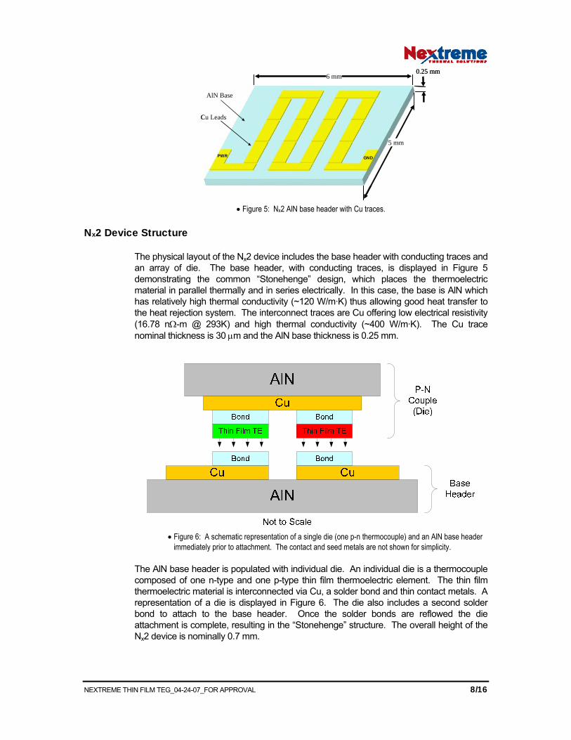
• Figure 5: Nx2 AlN base header with Cu traces.
Nx2 Device Structure
The physical layout of the Nx2 device includes the base header with conducting traces and an array of die. The base header, with conducting traces, is displayed in Figure 5 demonstrating the common “Stonehenge” design, which places the thermoelectric material in parallel thermally and in series electrically. In this case, the base is AlN which has relatively high thermal conductivity (~120 W/m·K) thus allowing good heat transfer to the heat rejection system. The interconnect traces are Cu offering low electrical resistivity (16.78 nΩ-m @ 293K) and high thermal conductivity (~400 W/m·K). The Cu trace nominal thickness is 30 μm and the AlN base thickness is 0.25 mm.
• Figure 6: A schematic representation of a single die (one p-n thermocouple) and an AlN base header
immediately prior to attachment. The contact and seed metals are not shown for simplicity.
The AlN base header is populated with individual die. An individual die is a thermocouple composed of one n-type and one p-type thin film thermoelectric element. The thin film thermoelectric material is interconnected via Cu, a solder bond and thin contact metals. A representation of a die is displayed in Figure 6. The die also includes a second solder bond to attach to the base header. Once the solder bonds are reflowed the die attachment is complete, resulting in the “Stonehenge” structure. The overall height of the Nx2 device is nominally 0.7 mm.

NEXTREME THIN FILM TEG_04-24-07_FOR APPROVAL 9/16
Nx2 Design
The Nx2 design is illustrated in Figure 7. Individual die each consist of a single p-n thermocouple (see Figure 1) with dimensions of 0.45 mm x 0.45 mm. The top surface of the die is AlN, which is the Nx2 interface to a heat source. The AlN base header is the Nx2 interface to a heat rejection system. Following the die attachment process, wires are attached to the bond pads. A picture of an actual, completed Nx2 device is shown in Figure 8.
GNDPWR GNDPWR
• Figure 7: An illustration of an AlN base header populated with individual die.
• Figure 8: A picture of a completed Nx2 device.
Numerical Modeling
FEA modeling can be conducted to analyze the performance of a proposed design for conditions specified. For example, for an application with a 120 K temperature difference, the FEA model showed that 502 mW are generated by the Nx2 device at 0.51 volts. The voltage profile of this case can be seen in Figure 9 below. The negative values shown in the figure simply reflect the polarity of the measurement. The power output results from this simulation are higher than those specified for the proposed Nx2-Alpha design discussed below. This can be attributed to the use of more idealized thermal interface assumptions in the model. A similar approach to the cooling device modeling resulted in strong agreement between experimental and FEA modeled results.

NEXTREME THIN FILM TEG_04-24-07_FOR APPROVAL 10/16
• Figure 9: FEA voltage plot from underfilled 4x4 generator.
Thin Film TEG Results – Nx2
Power Test Method
To test the ability of the Nx2 device to convert thermal energy to electrical energy, an (electrical) power test system was used. The power test system (Q-meter), displayed in Figure 10, includes a heat source and a heat rejection system. A brief description of the thermal column through which heat flows is provided here, as well as the detail involved in preparing the device under test (Figure 11).
Water Cooled Heat Sink
Nx2 Device
Q-Meter Thermocouples
Heater
Water Cooled Heat Sink
Nx2 Device
Q-Meter Thermocouples
HeaterHeaterHeater
• Figure 10: Illustration of the power test system used to characterize the Nx2 device.
The heat source is comprised of an electrical heater with the temperature controlled through an applied voltage (Variac). The source makes contact with the AlN on the top side of the die in the Nx2 device. A unified AlN header is used inorder to establish good uniform thermal contact between the heater and the top of the 4x4 die array. The unified AlN header is dressed with thermal interface material (TIM). The heater, also dressed with

NEXTREME THIN FILM TEG_04-24-07_FOR APPROVAL 11/16
TIM, is placed into contact with the unified AlN header. A thermocouple (T/C) is placed in contact with the AlN unified header to measure the “hot side” temperature (Th). The presence of the unified AlN header adds to interfacial heat flow losses which negatively impact the energy conversion efficiency.
TIM
TIM
Solder
• Figure 11: A cross-sectional representation of an Nx2 device prepared for power testing. Not drawn to scale.
The AlN base header of the Nx2 device is soldered to the top of the Q-meter (see Figure 10 and description below). The base of the header is dressed with TIM prior to soldering. A T/C is placed in contact with the AlN base header to measure the “cold side” temperature (Tc).
The heat rejection system is comprised of a Q-meter (Figure 10) mounted on a liquid cooled cold plate. The Q-meter has five T/C’s attached at specific locations along its length. This T/C arrangement provides a measurement of the temperature gradient along the Q-meter from which an accurate temperature at the tip of the Q-meter can be extrapolated. The tip of the Q-meter is the location of the AlN base header for the Nx2 device. Collectively, the heater and heat rejection systems constitute the operating conditions to which Nx2 device performance can be tested. The difference between Th and Tc is the external ΔT (ΔText) discussed previously. Careful attention to detail is exercised while preparing the test system and the Nx2 device to minimize heat flow losses.
The electrical power output testing is accomplished in two steps: 1) Measurement of the open circuit voltage (Voc); 2) Measurement of the short circuit current (Isc). Once the operating conditions reach thermal equilibrium (i.e., stable Th and Tc), a dc voltage measurement unit is used to collect Voc. The estimated error in Voc is ±5 mV. This is followed by a switch in metrology instrumentation, where a curve tracer is used to generate a load-line from the Nx2 device. An example of a load line is displayed in Figure 12 where the horizontal axis is “Voltage” and the vertical axis is “Current”. At I = 0, a verification of Voc can be obtained. The point where the Nx2 load line intersects the “Current” axis (V = 0) is Isc. The estimated error in Isc is ±5 mA. The process of collecting Voc and Isc occurs for each ΔT. The electrical output power is then calculated using the following expression for the maximum power:
Equation 13 SCOC IVP ⋅=41

NEXTREME THIN FILM TEG_04-24-07_FOR APPROVAL 12/16
To obtain the efficiency of energy conversion at each ΔT, the Nx2 device was driven at ½ Isc and ΔT was increased slightly until the potential generated by the Nx2 device reached ½ Voc. Using this approach to determine η, the basic assumption is the heat flow through the Q-meter (i.e., K·ΔT) matches the heat input to the Nx2 device when Voc and Isc were initially measured. The efficiency (η) is then given by
Equation 14 inQ
P=η
where P is determined from The heat rejection system is comprised of a Q-meter (Figure 10) mounted on a liquid cooled cold plate. The Q-meter has five T/C’s attached at specific locations along its length. This T/C arrangement provides a measurement of the temperature gradient along the Q-meter from which an accurate temperature at the tip of the Q-meter can be extrapolated. The tip of the Q-meter is the location of the AlN base header for the Nx2 device. Collectively, the heater and heat rejection systems constitute the operating conditions to which Nx2 device performance can be tested. The difference between Th and Tc is the external ΔT (ΔText) discussed previously. Careful attention to detail is exercised while preparing the test system and the Nx2 device to minimize heat flow losses.
The electrical power output testing is accomplished in two steps: 1) Measurement of the open circuit voltage (Voc); 2) Measurement of the short circuit current (Isc). Once the operating conditions reach thermal equilibrium (i.e., stable Th and Tc), a dc voltage measurement unit is used to collect Voc. The estimated error in Voc is ±5 mV. This is followed by a switch in metrology instrumentation, where a curve tracer is used to generate a load-line from the Nx2 device. An example of a load line is displayed in Figure 12 where the horizontal axis is “Voltage” and the vertical axis is “Current”. At I = 0, a verification of Voc can be obtained. The point where the Nx2 load line intersects the “Current” axis (V = 0) is Isc. The estimated error in Isc is ±5 mA. The process of collecting Voc and Isc occurs for each ΔT. The electrical output power is then calculated using the following expression for the maximum power:
Equation 13 and Qout, which is approximated to be equal to Qin , is determined from the Q-meter.
Employing the power test system, the Nx2 device performance can be compared to the specifications given in Table 1. In addition, device characterization data can be collected to provide insight to the available application space.

NEXTREME THIN FILM TEG_04-24-07_FOR APPROVAL 13/16
V
I
Isc
Voc
Load Line
V
I
Isc
Voc
Load Line
• Figure 12: An example of a load line collected from the Nx2 device that is used to determine Isc.
Nx2 Power Test Results
The Nx2 power testing was carried out in two steps. The first step consisted of Nx2 device characterization. The characterization data includes measured parameters and module characteristics calculated over a range of ΔText’s. The second step consisted of measurement and calculation of device parameters specified in Table 1 – in this case for ΔText = 70 K and 120 K, respectively.
Nx2 Device Characterization
Numerous Nx2 devices were assembled for device characterization and tested over the range ΔT = 1 – 153 K. The measured parameters were: heater temperature, Thtr; top header temperature, Th; bottom header temperature, Tc; output heat, Q; open circuit voltage, Voc; and short circuit current, Isc.
Thtr is measured from a T/C embedded in the heater, Th from a T/C resting on the unified AlN header, and Tc from a T/C resting on the AlN base header. To improve thermal contact between the T/C to AlN headers, thermocouple paste was used at the tip of the T/C’s resting on the respective AlN headers (Figure 11).
Typically the output power as a function of ΔText is used to judge power device capability. A representative plot for the Nx2 device is displayed in Figure 13, where Tc < 41°C. The data points in Figure 13 are measured and line is a parabolic fit to Equation 15.
Equation 15 RTS
RVIV
P OCSCOC
⋅Δ⋅
=⋅
=⋅
=4
)(44
22
where,
Equation 16 TSRIV SCOC Δ⋅=⋅=
In Equation 15 and Equation 16, R is the device electrical resistance and S is the device Seebeck coefficient. The correlation coefficient (R2) in the lower right hand side of Figure

NEXTREME THIN FILM TEG_04-24-07_FOR APPROVAL 14/16
13 indicates that 99.94% of the variation in the data is accounted for in the parabolic fit as expected from Equation 15.
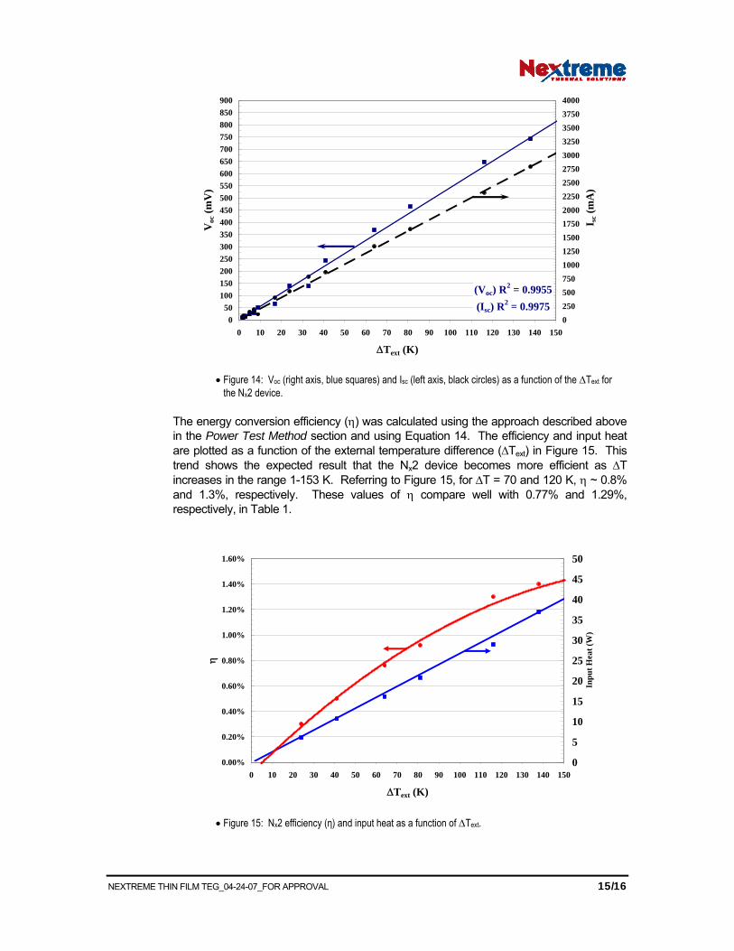
The parameters used to calculate the output power are, as indicated in Equation 15, Voc and Isc. Voc and Isc are shown in Figure 14 as a function of ΔText. Voc measurements are represented by blue squares and the solid blue line. Isc measurements are denoted by the black circles and the dashed black line. Linear behavior is expected from Equation 16 and the R2 values is > 0.99. Applying Equation 16, the slope of Voc versus ΔT is the device Seebeck coefficient (S). The Nx2 device has a Seebeck coefficient, S ≈ 5087 μV/K.
R2 = 0.99940
50
100
150
200
250
300
350
400
450
500
550
600
0 10 20 30 40 50 60 70 80 90 100 110 120 130 140 150
ΔText (K)
Pow
er (m
W)
• Figure 13: Nx2 output power as a function of external temperature difference (ΔT) across the device.
NEXTREME THIN FILM TEG_04-24-07_FOR APPROVAL 15/16
(Voc) R2 = 0.9955
(Isc) R2 = 0.9975
050
100150200250300350400450500550600650700750800850900
0 10 20 30 40 50 60 70 80 90 100 110 120 130 140 150
ΔText (K)
Voc
(mV
)
02505007501000125015001750200022502500275030003250350037504000
I sc (m
A)
• Figure 14: Voc (right axis, blue squares) and Isc (left axis, black circles) as a function of the ΔText for
the Nx2 device.
The energy conversion efficiency (η) was calculated using the approach described above in the Power Test Method section and using Equation 14. The efficiency and input heat are plotted as a function of the external temperature difference (ΔText) in Figure 15. This trend shows the expected result that the Nx2 device becomes more efficient as ΔT increases in the range 1-153 K. Referring to Figure 15, for ΔT = 70 and 120 K, η ~ 0.8% and 1.3%, respectively. These values of η compare well with 0.77% and 1.29%, respectively, in Table 1.
0.00%
0.20%
0.40%
0.60%
0.80%
1.00%
1.20%
1.40%
1.60%
0 10 20 30 40 50 60 70 80 90 100 110 120 130 140 150
ΔText (K)
η
0
5
10
15
20
25
30
35
40
45
50
Inpu
t Hea
t (W
)
• Figure 15: Nx2 efficiency (η) and input heat as a function of ΔText.

NEXTREME THIN FILM TEG_04-24-07_FOR APPROVAL 16/16
Nx2 Test Data Comparison to Specification (Table 1)
Power test data for the Nx2 devices is presented in this section, which is intended for comparison to the Nx2 specifications given in Table 1 for ΔText = 70 and 120 K.
Using Equation 15 and measured values for Voc and Isc, the Nx2 output powers for ΔText = 70 and 120 K were calculated (Figure 16). With the exception of one device at ΔText = 70 K, the Nx2 output power was above the minimum specified value. The output power of 50 mW at ΔText = 70 K was a result of the low value of Isc (498 mA). The low Isc was attributed to the appearance of a high device resistance due to poor wire attachment to the metrology system.
0
50
100
150
200
250
300
350
400
450
500
1783 1785 1786 1787 1788 1790 1791 1792 1793 1794 1795 1796 1797 1798
Nx2 Device ID
Pow
er (m
W)
ΔText = 120 K
ΔText = 70 K
174 mW @ ΔText = 120 K
58 mW @ ΔText = 70 K
• Figure 16: Output power for ΔT = 70 and 120 K for a series of Nx2 devices. The minimum
specification limits from Table 1 are included in the plot.
Conclusion
Thin film thermoelectric materials at Nextreme have matured to the point where it is feasible to design and build fully functioning power generating devices incorporating thin film thermoelectric technology. Thin film thermoelectric materials are 100 times thinner than their bulk material counterpart, yet they are able to achieve device-level performance that far exceeds bulk performance in terms of power density and almost equal in terms of ΔT.
Nextreme has demonstrated the ability to design and fabricate thermoelectric generators that meet expected performance based on analytical and FEA modeling results. In an optimized thermal environment, where heat rejection is well matched to the heat flux specification of the TEG design, power levels of actual devices consistently met or exceeded target specifications. Power levels >100 mW at ΔT =70 K and >300 mW at ΔT=120 K are achievable with modules that measured 3.5 mm x 3.5 mm in size, corresponding to power densities of ~1-3 W/cm2.

NEXTREME THIN FILM TEG_04-24-07_FOR APPROVAL I
Appendix: Thin Film Thermoelectric Design Considerations
Basic Equations Governing TEG Performance
A thermoelectric generator produces electrical power because of the Seebeck effect. The Seebeck voltage (Voc, measured under open circuit conditions) produced is directly proportional to the temperature difference.
Equation 17 TSVOC Δ=
where S represents the device Seebeck coefficient. During operation of the TEG, the output voltage is reduced by the Ohmic voltage drop due to the internal resistance of the device. Consequently, the voltage at maximum power is about half that of the open circuit voltage VOC (VOC=SΔT≈2Vmax) and the maximum power changes with temperature difference as ∆T2.
Equation 18 RTS
RV
RVP OC
44
2222max Δ
===
The efficiency of a TEG is governed by the properties of the thermoelectric materials and the temperature drop across them. The temperature difference, ∆T between the hot side (Th) and the cold side (Tc) sets the upper limit of efficiency through the Carnot efficiency ηC = ΔT/Th. The thermoelectric material governs how close the efficiency can be to Carnot primarily through the thermoelectric figure of merit, Z, defined as
Equation 19 ρ
αk
Z2
=
where the relevant materials properties are the Seebeck coefficient α, the thermal conductivity k, and electrical resistivity ρ, all of which vary with temperature. The Seebeck coefficient of the device S is the sum of the Seebeck coefficients of each thermoelectric element, or approximately S = 2nα, where n is the number of thermocouples, each one of which has an n-type thermoelectric element and a p-type thermoelectric element.
The efficiency, η, for power generation is defined as the electrical power output divided by the thermal power supplied. The electrical power P is easily measured and is the product of the current, I, and voltage output, V, of the generator. The heat, Q, into the device, is much more difficult to measure and frequently estimated by calculation. Q is the sum of the Peltier heat term and the solid conduction term with a correction for Joule heating.
Equation 20 RITKITn
IVQP
h2
212 −Δ+
==α
η
where K is the thermal conductance (kA/L) and R is the electrical resistance (ρL/A) of the module. For a material with thermoelectric properties (α, ρ, k) constant with respect to temperature the maximum efficiency is approximately

NEXTREME THIN FILM TEG_04-24-07_FOR APPROVAL II
Equation 21
ZTT
T
M4
22 −
Δ+
Δ=η
where TM is the average temperature across the device, (Th + Tc)/2.
If the efficiency and ∆T are measured then an effective Z can be calculated. Assuming Z remains relatively constant in temperature, this equation can then be used to calculate efficiency for any given ∆T.
Power Output
Many Nextreme 4x4 devices (16 PN couples) have been characterized for power generation with temperature differences up to 200K while Tc was maintained constant at 30ºC (303K). The open circuit voltage, the AC resistance, and performance driving a load are measured for a given temperature difference. The Nextreme devices show consistently high power output per unit area, as is expected due to the short thermoelectric element thickness, L. A typical device has the following performance:
V-open circuit (mV) R (mΩ) ∆T (K)
135 151 36 381 163 94 504 156 132 619 148 189
From these measured values and the equations above, the effective properties can be calculated.
α (µV/K) R (m Ω) 120 155
Using these values, the power output of the device for a variety of temperature differences can be reliably estimated as shown below.
0.00
100.00
200.00
300.00
400.00
500.00
600.00
700.00
800.00
0 20 40 60 80 100 120 140 160 180
DT (K)
Pow
er O
utpu
t (m
W)
• Figure 17: Power output calculations for a 4x4 thin film thermoelectric power generator.
Because output power scales with the input heat flux, it is possible to design a high output power module that requires an impracticably high heat flux source. Likewise, at very large
NEXTREME THIN FILM TEG_04-24-07_FOR APPROVAL III
heat fluxes, demands on heat sink performance become unreasonable. Preserving this balance between practical heat sources and sinks has been a goal in Nextreme device design, resulted in the selection of 150 W/cm2 as the maximum input heat flux.
The design approach for packaging requires a similar balance between competing demands, in this case, between performance and ruggedness. An important question to be answered is how to apply an underfill, expected to considerably strengthen the module, without causing excessive performance degradation.
Optimizing Performance and Ruggedness
Thin-film thermoelectric devices can be engineered to deliver maximum output power to a load under very high input heat flux conditions. Provided such heat sources are available, as well as heat sinks capable of dissipating such large heat fluxes, very large output powers can be obtained.
Equation 3 shows that the output power is equal to the product of power conversion efficiency (η) and the total heat flowing through the device (Q).
Equation 22 shows that for any particular ΔT, the amount of heat transfer due to conduction, Q, can be increased by improving the module thermal conductance, K.
Equation 22 TKQ Δ⋅=
For an underfilled device, the total thermal conductance of the module, K, is the sum of the thermoelectric conductance (KTE) and underfill conductance (Kuf):
Equation 23 ufufufTETETEufTE /LAk /LAk K K K +=+=
Any heat flowing through the underfill decreases efficiency, and should be minimized. So, as shown in Equation 23, the total heat available for power conversion is increased when the thermoelectric thermal conductance is increased. Since the thermal conductivity (kTE) is an intrinsic material property, not a design parameter, the thermoelectric area to length ratio (ATE/LTE) is the primary device design parameter that can be manipulated to control Q. As discussed previously, the total active area (ATE) of the module can be related to the packing fraction (f) (see Equation 6).

NEXTREME THIN FILM TEG_04-24-07_FOR APPROVAL IV
Output Power Density vs Packing FractionVarying Packing Fraction Varies Heat Flux
02468
10121416
0.0 0.1 0.2 0.3 0.4 0.5 0.6
Packing FractionO
utpu
t Pow
er (W
/cm
2)
70C120C
• Figure 18: Output Power vs. Packing Fraction (f)
Figure 18 shows a plot of the output power as a function of packing fraction at 70 and 120ºC. Increasing the packing fraction increases the module thermal conductance, K, and thereby increases the input heat flux and the output power.
This same data is shown in Figure 19 as a function of input heat flux. Finally, Figure 20 shows the impact of packing fraction on the input heat flux. It is clear from these figures that higher output powers are possible if the module active area packing fraction is increased, which will increase the input heat flux.
Thus, packing fraction is a design parameter that needs to be tailored to the heat flux environment available within a particular application. Furthermore, the system heat source and heat sink thermal resistances have a significant impact on optimal thermoelectric design. If these boundary conditions are known, the module can be designed to produce maximum power for the given heat flux available. At Nextreme, for the purposes of design, 150 W/cm2 has chosen as the peak input heat flux, and the device thermal conductance was varied to produce a ΔT of 200K at that flux.
As shown in Figure 19 and Figure 20, the peak input heat flux can be set by simply varying the device packing fraction. This is easily accomplished by changing the TE die active area, and requires minimal redesign. This provides great flexibility when optimizing the module for specific applications.

NEXTREME THIN FILM TEG_04-24-07_FOR APPROVAL V
Power vs Heat FluxVarying Flux by Increasing Packing Fraction
0
2
4
6
8
10
12
14
16
0 200 400 600 800 1000
Input Heat Flux (W/cm2)O
utpu
t Pow
er (W
/cm
2)
70C120C
• Figure 19: Output Power vs. Input Heat Flux
Input Heat Flux vs Packing FractionVarying Flux by Increasing Packing Fraction
0
200
400
600
800
1000
0.0 0.1 0.2 0.3 0.4 0.5 0.6
Packing Fraction
Inpu
t Hea
t Flu
x (W
)
70C120C
• Figure 20: Input Heat Flux vs. Packing Fraction
Maximizing Performance – Efficiency
Thermoelectric power generation efficiency is determined by material characteristics, package thermal parasitics and operating conditions.
Obtaining continued increases in materials efficiency is the focus of ongoing, long term efforts. For example, recently developed thicker films, as well as new, nanostructured films (see materials improvements in Figure 3), seem particularly promising in this regard. As such improvements are demonstrated, they will be incorporated into the technology as appropriate.
Efficiency is directly proportional to the temperature difference (ΔT) across the module. To achieve the highest operating efficiency possible, the module and packaging should be designed to maximize the temperature across the module. Accordingly, an important design goal is the reduction of thermal parasitics from packaging that decrease the operating ΔT, both inside and outside the device.

NEXTREME THIN FILM TEG_04-24-07_FOR APPROVAL VI
To make practical, rugged, field-deployable thermoelectric modules, without compromising performance and efficiency, each material used must be carefully considered. The thermal performance of the bulk material and any interfaces must be optimized to maximize the amount of heat going through the active thermoelectric material, and minimizing the amount heat that is diverted through the passive packaging materials. In this way reductions in ΔT, and in turn, power output and efficiency, can be mitigated.

NEXTREME THIN FILM TEG_04-24-07_FOR APPROVAL VII
Nextreme Thermal Solutions
Nextreme Thermal Solutions manufactures thin-film thermoelectric components that address the most challenging thermal management and power generation needs of the semiconductor, photonics, consumer and defense/aerospace industries. Nextreme's miniature, thin-film eTEC™ offers an industry first — a micro-refrigerator the size of a piece of confetti that enables active, solid-state temperature control or power generation on a micro-scale, in close proximity to a heat source. The eTEC operates as point-specific heat pump for rapid cooling or heating of semiconductors and other electronics; for thermal management of fiber-optic laser controls and integrated optoelectronics; or for power generation by converting otherwise wasted heat into useful electricity.
Unlike conventional thermoelectric components made by manually assembling individual pellets together, Nextreme uses semiconductor processing techniques to provide pin-point thermal control for high heat fluxes to increase product performance, reliability and yield.
The eTEC structure optimizes thermal and electronic transport for enhanced thermoelectric performance and offers an ultra-small footprint (as small as 0.3 mm x 0.3 mm x 0.1 mm), delivering uniquely-high power densities, microsecond response times and semiconductor fabrication scalability. In cooling mode the eTEC holds off as much as 40ºC and pumps a maximum heat flux of 175 W/cm2
as compared to less than 15 W/cm2 for conventional technology. Some designs demonstrate as much as 400 W/cm2
of pumping power. Deployed as a thermoelectric generator (TEG) the Nextreme device can perform in high-heat flux applications where there are no conventional solutions, using waste heat to deliver more than 3 W/cm2
of electrical power. The technical basis for this new range of performance is displacement of high heat flux (50 – 100 W/cm2) at a high efficiency (coefficient of performance, COP, greater than 1).
Headquartered in Research Triangle Park, Nextreme Thermal Solutions (www.nextreme.com) founded in December of 2004 to commercialize the nanotechnology that was under development for more than 10 years at RTI International (www.rti.org).


![Chalcogenide Flexible Thin Film Thermoelectric Device ... · thin film when deposited at 200oC. Schematic of Sputtering, reprinted from [2] Thin Film Analysis and Device Characterisations](https://img.pdfslide.us/doc/110x75/5fcf5c7b1616563f4f26467d/chalcogenide-flexible-thin-film-thermoelectric-device-thin-film-when-deposited.jpg)