Embed Size (px)
Citation preview

1 www.lairdtech.com Laird Technologies
THIN FILM THERMOELECTRIC HANDBOOK

2 www.lairdtech.com Laird Technologies
Americas: +1 888.246.9050
Europe: +46 31 420530
Asia: +86 755 2714.1166
THR-UM-THIN FILM THERMOELECTRIC 1212

3 www.lairdtech.com Laird Technologies
Contents
Introduction .......................................................................... 4
Advantages of Thin Film Technology .................... 5
Thermoelectric Cooling .......................................... 5
System Level Considerations ................................ 6
Thermal Management Design ............................................. 7
Heat Flow .............................................................. 7
Passive Cooling ..................................................... 8
Active Cooling ...................................................... 8
Design Considerations .......................................... 9
Module Handling & Assembly ............................................ 11
Parts & Supplies List ........................................... 12
Assembly Procedure ........................................... 13
Precautions .......................................................... 14
Temperature Sensing ........................................................ 16
Integration Examples ........................................... 16
Reliability ........................................................................... 19
Revision History
Revision Description
1 8/30/2012 – Initial Version

4 www.lairdtech.com Laird Technologies
Thin Film Thermoelectrics
As components, packages and systems continue to shrink in size, the heat generated in these dense
electronic systems can be quite large and can lead to a significant rise in temperatures that in turn can
cause device and system-level failures.
Heat has always been an issue for system designers, but only recently has the problem become so
severe that thermal management solutions can no longer be introduced as an afterthought. Thermal
management must be considered from the beginning of the design process in order to avoid causing
severe problems at the system level. This is an important consideration because at the system level,
the thermal operating space is more limited (i.e. the temperatures that can be tolerated) and any
solution employed at the system is likely to be more expensive than one implemented at the chip level.
A new approach to thermal management involves embedding thermal management functionality deep
inside an electronic component at the source of the heat using thin film thermoelectric devices.
Introduction
TEMs (thermoelectric modules) are solid-state heat pumps that operate using the Peltier effect. When
an electric current is driven through a circuit containing two dissimilar materials, heat is absorbed at one
junction (the cold side) and released at the other junction (the hot side). The design of most Peltier
devices requires the use of both an n-type semiconductor and a p-type semiconductor. Since heat
naturally flows down a temperature gradient from hot to cold, a TEM’s ability to move heat from cold to
hot in a solid-state fashion is unique. By reversing the polarity of the applied DC current, heating is also
possible. This attribute is especially useful for applications requiring both cooling and heating to
maintain precise temperature control.
Conventional TEMs, sometimes referred to as ―bulk‖ TEMs, have been used for decades to control the
temperature of electronics. However, as the size and power density requirements of new applications
are changing, conventional bulk thermoelectric technology has not kept pace. In some instances,
designers choose to place the cooling device outside the package if it is too large to be placed inside.
Cooling the device by cooling the entire package is at best an inefficient method for thermal
management and often leads to over sizing of the TEM and input power requirements, which results in
more waste heat in the system.

5 www.lairdtech.com Laird Technologies
Advantages of Thin Film Technology
Conversely, thin film thermoelectrics target the source of the heat flux to provide thermal management
and control. These embeddable TEMs use semiconductor processing techniques to create a
nano-structured thin film used for the P and N legs. Thin film TEMs are typically 5 to 20µm thick, versus
200µm for conventional bulk TEMs, resulting in several differences. The heat flux, which is inversely
proportional to the thickness of the thermoelectric material, is more than 20 times greater than bulk
TEMs. Thin film TEMs can also pump a maximum heat flux of 100 to 400W/cm² versus less than
10W/cm² for conventional bulk TEMs. Thin film TEMs can operate in a high coefficient of performance
(COP) regime and still pump a reasonably high heat flux of 20 to 40 W/cm². COP is a measure of
efficiency defined as cooling power divided by input power.
Figure 1:Ccomparison of thin film vs bulk device
Depending on the design, thin film TEMs may have thermal response times as low as milliseconds
enabling very rapid cooling and heating to maintain precise temperature control. They are known to
have higher heat pumping capability than standard bulk TEMs, but for temperature control applications,
the superior switching speed of the devices may ultimately prove to be their most valuable asset.
Thermoelectric Cooling
The most basic representation of the operational space for a thermoelectric module is a performance
chart as shown in Figure 2.
Figure 2: TEM Performance Chart.
The load line represents the ΔT and power pumped conditions possible for a given TEM drive current.
At the maximum drive current for the module, the load line is generated from two key parameters: 1) the
maximum power the device can pump, Qmax; and, 2) the maximum temperature difference that the
device can sustain between its top and bottom substrates, ΔTmax.
The load line defines the operational space for TEMs and is the best and most usual way to illustrate
cooling capacity for a particular temperature condition.

6 www.lairdtech.com Laird Technologies
System Level Considerations
The TEM, being an active thermal device, creates a thermal inversion that dramatically changes the
thermal profile inside the package. Figure 3 shows a comparison of the thermal profile through the
cross section of the module in two cases, a) with no TEM, or in other words, a passive solution only,
and b) with a TEM actively cooling the junction. It can be clearly seen that the introduction of the TEM
provides a substantial net cooling benefit.
Figure 3: Temperature profiles through the cross section of a package from the junction to the case (θJC), and case to ambient (θCA) without (a)
and with (b) a TEM. The temperature inversion created by the TEM lowers the junction temperature relative to the no-TEM case.
The heat that is pumped by the device and the additional heat created by the TEM in the course of
pumping that heat will need to be rejected into the system. Since the performance of the module can be
improved by providing a good thermal path for the heat rejected, it is beneficial to provide high
thermally conductive pathways. For small packages, this is typically accomplished through the
electrical connections themselves, and depending on the operating characteristics, this level of thermal
management might be sufficient. For packages with higher heat densities, thermally-conductive
feed-throughs or posts may be needed to remove the heat.
7 www.lairdtech.com Laird Technologies
Thin Film Thermal Management Design
In order to understand the design challenges facing engineers in the electronics industry, we need to
first look at the way heat moves or flows through a material system, and to do this we need to look at
the forces that govern that movement. Heat has always been an issue for system designers, but only
recently has the problem become so severe that thermal management solutions can no longer be
introduced as an afterthought. Heat flux must be looked at from the beginning of the design process.
Heat flowing through a material will always create a temperature gradient across that material and will
do so in a continuous manner as it flows from one material to another.
Designing in a thermal management system today is a cumbersome exercise where the means for
moving the heat and the manner and location in which we reject the heat must be considered early in
the design cycle in order to avoid causing severe problems at the system level. This is an important
consideration because at the system level the thermal operating space is more restricted with the
temperatures that can be tolerated and any thermal conducted at the system level is likely to be more
expensive than one implemented at the chip level.
Unfortunately the management of heat in a system is at times a lot like pushing jelly. You can press it
down in one direction but it will just flow in another. To see why this is so, we will look at the rules for
heat flow in a material system.
Heat Flow in a Material System
The heat equation is an important partial differential equation describing the distribution of heat (or
variation in temperature) in a given region over time. For a function u (x, y, z, t), which is a
measurement of the temperature T, of three spatial variables (x, y, z), and the time variable t, the heat
equation is
u = u(t, x, y, z) is temperature as a function of time and space; or equivalently
Here k is a constant.
The other important governing equation is
Q = U + W
Heat flow is equal to the work on the system plus the change in internal energy of the system. Hence, in
thermodynamics, the change in heat is equivalent to the heat flowing into the system. Combining these
two equations and in the absence of any work being performed, Q is proportional to the change in
temperature. We won’t provide the derivation here since it is to be found everywhere in the literature
but we then arrive at:
Q = kΔT
Hence for passive systems, cooling by the conduction of heat is a linear function of temperature and a
constant related to the material properties of the solid. This constant k may be a function of many
variables including T, P, and V.

8 www.lairdtech.com Laird Technologies
Passive Cooling
The primary systems used for passive cooling of electronic and optoelectronic systems are materials
configured as thermal interface materials (TIM), heat spreaders and heat exchangers. Each perform a
different function for removing heat from a system.
Heat exchangers may be an environment (e.g. liquid or air) or object that absorbs and then dissipates
heat while in physical or thermal contact. This may occur in different ways including direct and radiant
transfer of heat. A heat exchanger’s performance is a function of material, geometry, and the overall
surface heat transfer coefficient along with the temperature of the heat sink. Generally, forced
convection heat sink thermal performance is improved by increasing the thermal conductivity of the
heat exchanger materials and increasing the surface area.
Thermal interface material (TIM) is used to fill the gaps between thermal transfer surfaces, such as
between microprocessors and heat sinks, in order to increase thermal transfer efficiency. These gaps
are normally filled with air, which is a very poor conductor of heat. The most common TIM is thermal
grease, typically silicone oil filled with aluminum oxide, zinc oxide, or boron nitride.
Heat spreaders, most often simple metal plates, have high-thermal conductivity. Carbon-based heat
spreaders having anisotropic characteristics are also being used. They act as a heat exchanger moving
heat between localized heat and a secondary heat exchanger that is larger in area.
For all the passive components described above, heat will move through them as described by the
general rules below:
1. There has to be a temperature difference; heat will only flow if there is a temperature difference
2. Heat always flows from a higher temperature to a lower temperature
3. The rate of flow is proportional to the difference in temperature
4. The flow of heat may be caused or assisted by both active and passive means
Active Cooling and Package Size
As overall sizes of electronic devices shrink, the size of the thermal management system must also
shrink. Given that passive heat removal is only a linear function over distance of the temperature
difference, work must be put into the system to obtain a greater rate of cooling and yield a smaller
device.
One such example for optoelectronics of the continuing reduction in package size is shown below in
Figure 4. In some instances, designers choose to place the cooling device outside the package
because it is too large to be placed inside.
Figure 4: Size comparisons of optoelectronic packages and thermoelectric modules. From left to right, TO-56, TOSA and butterfly package

9 www.lairdtech.com Laird Technologies
An active thermal management device, such as a thermoelectric module (TEM), has been employed to
provide this additional heat pumping and temperature stabilization capability. A simple example of the
type of heat pumping and temperature control offered by a TEM and its ability to cool a device is shown
in Figure 5.
Figure 5: TD is the temperature of the device to be cooled; TC is the temperature of the cold side of the TEM; TH is the temperature of the hot
side of the TEM; and TA is the temperature of the ambient or surrounding environment where the heat is to be dumped.
A Comparison of Active and Passive Cooling
As shown above, thermal management solutions for electronics may be divided into two types of
systems: active and passive. With the exception of fans, which are usually combined with heat sinks,
most of today's thermal management systems are passive types. Conduction-based thermal
management systems, such as thermal interface materials (TIMs), are used to improve the flow of heat
from one location to another and greatly enhance the efficiency of the overall thermal management
system. However, convection-based systems have the drawback of allowing heat to flow in an
uncontrolled manner from one level to the next.
These systems have served the industry well but have the drawback of removing not only the heat that
is limiting device performance but also any of the heat from the surrounding area which likely is not
limiting the device or system performance.
One solution is to apply an active device as a localized thermal management solution. This could be
applied inside the electronic package. To reduce the cooling needed at the system and building levels,
we need to reduce the amount of heat extracted from the die. Die are typically cooled to keep their
operating frequency near its peak. However, this peak frequency is typically limited by the temperature
within one of the hot spots on the die and not the temperature across the entire die.
If instead of extracting the heat from the die as a whole, we are able to extract the heat from the hot
spot only, we will create a smaller system-level problem to deal with and subsequently have a smaller
building thermal management problem.
Design Considerations
One of the drawbacks of thermoelectric devices is that in order to cool, they consume power. This
power adds to whatever power is being pumped out of the cooling zone, so at the larger, system level
more heat has to be dissipated with a TEM in operation than without one.
If TEMs are applied to cool devices in the same manner as passive thermal components, then the heat
dissipation becomes a much larger problem at the system than at the chip level. A more cost-effective
and efficient approach — and one that is only possible with TEMs — would be to cool only what is
necessary. In other words, scale the thermal management system to the size of the heat problem.
TA
TH
TC
TD
Distance
Temperature
TA
TH
TC
TD
Distance
Temperature
10 www.lairdtech.com Laird Technologies
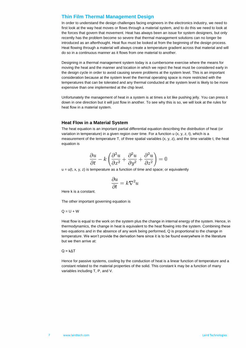
This can be illustrated by looking at the coefficient of performance (COP) of a TEM, which is defined as:
in
pumped
P
QCOP =
A TEM will pump a certain amount of heat, Q, and add an additional amount of heat, Q*COP to move
this heat. This is a result of the inherent inefficiency in all engines. As a result, bulk TEMs are often sold
as systems that include the TEM and a heat transfer mechanism such as a fan and heat sink or liquid
heat exchanger. The value of the TEM in this case is that it can deliver sub-ambient temperatures and
provide active temperature control but at the cost of increasing the system level heat transfer problem.
Because heat in the passive case flows linearly, any thermal resistance between the TEM and the heat
source will have a temperature drop across it. This will act to increase the temperature difference that
the TEM must pull. As already mentioned, the TEM is a heat pump removing heat in a manner whose
efficiency depends upon the temperature difference it is required to generate. Minimizing this
temperature difference will improve the efficiency of the TEM and reduce the additional heat added at
the system level.
Integration of a TEM close to the heat source is the key to improving a TEMs operational efficiency.
Adding an additional heat transfer system defeats the purpose of the integration. As such, careful
attention has to be paid to the characteristics of the heat transfer problem, the design of the thin film
solution and also the design of the device package. When these three issues are addressed in tandem;
ideally at the time of product design and development, significant performance improvements can be
achieved.

11 www.lairdtech.com Laird Technologies
Module Handling and Assembly
Thin film thermoelectric modules have extremely small form factors with footprints smaller than 10 mm2.
These devices are only 0.6mm high, making them the thinnest thermoelectric modules available on the
market today. Due to their small form factor, care must be taken when handling and assembling
modules into sub-assemblies for validation testing and production use.
Figure 6 shows a typical thin film thermoelectric module. Please note the location of the primary and
secondary headers, which are referenced in the assembly instructions that follow.
Figure 6: Typical Thin film Thermoelectric Module.
Figure 7 shows a rendered image of an HV56 in a ―generic thermal package‖ consisting of two metal
plates with spacers and the eTECTM
(with wires) sandwiched between. The lower metal plate is
described as the ―heat-rejection surface‖ while the upper plate is the ―temperature controlled surface‖.
The figure indicates typical components used during package assembly, including spacers, hard
solders, and liquid metals.
Figure 7: A generic thermal package.

12 www.lairdtech.com Laird Technologies
The assembly procedure that follows describes a method for fabricating a thermoelectric assembly as
shown in the figure above where a thin film thermoelectric device is packaged between thermally
conductive plates. These plates could represent separate heat-spreaders or could be an integral part of
the heat-exchangers or temperature controlled target. The package has been optimized to meet the
conflicting requirements of highly conductive thermal interfaces while allowing for mechanical isolation
of the eTECTM
.
Suggested Parts and Supplies List
Solder – available from Indium Corporation in wire or foil preform
• InSn alloy #1E (52/48), MP 118°C
• BiSn alloy #281 (58/42), MP 138°C
• PbSn alloy #106 (63/37), MP 183°C
Flux – available from Indium Corporation
• For InSn and BiSn: TacFlux012
• For PbSn: TacFlux020 or 5RMA
ArticSilver Epoxy
• New Egg, catalog #N82E16835100005
Liquid Metal
• GaSn : Alfa Aesar, stock #18161
• GaInSnZn: Indium Corporation alloy #46L
3M Kapton tape
• Digi-Key # 3M541312-ND
Foam swab
• VWR, cat # TWTX751B
Mechanical Supports
• Fralock, 26 mil thick Cirlex® (custom cut)
Tweezers
• TDI International, part #5C-SA

13 www.lairdtech.com Laird Technologies
Assembly Procedure
The recommended assembly procedure is described below:
1. Solder the eTEC to the heat rejection surface
The high heat fluxes provided by thin film eTECs require a metallic interface for optimal thermal
performance. Non-metallic contacts will reduce the effective performance (ΔT) of the eTEC. Several
solders and related fluxes that have been used successfully are listed in the parts list above. The bond
line should be kept as thin as practical for minimal thermal resistance.
It’s important to only handle the primary and not the secondary header of the eTEC. Precision tweezers
that we have found to be appropriate for eTECs are recommended in the parts list above.
2. Attach the mechanical spacers to the heat rejection surface
Thermal expansion of the heat rejection and temperature controlled surfaces will differ due to different
temperatures and possibly also material properties of these surfaces. eTECs are more robust in
compression than in shear, due to the material properties that enable high heat flux densities. It is
therefore necessary to provide mechanical spacers between the heat rejection and temperature
controlled surfaces to avoid transferring shear forces to the eTEC.
There is a tradeoff between mechanical strength and thermal performance. These mechanical spacers
are also a thermal shunt that can reduce ΔT if a material with high thermal conductivity is used. We
therefore recommend the use of Cirlex®1 (see the parts list above) with a thermal conductivity of 0.17
W/m-K. An epoxy that we have used successfully with Cirlex® and different metallic surfaces is also
recommended in the parts list above.
3. Coat the secondary header of the eTEC with Liquid Metal
We recommend the use of GaSn or GaInSnZn liquid metal as an interface between the secondary
header of the eTEC and the controlled temperature surface to provide high thermal conductivity while
protecting the eTEC from high shear forces. GaSn is preferred when the controlled temperature surface
is always at or above room temperature (22°C). GaInSnZn is preferred for lower temperatures because
it has a lower melting point. Gold coated eTECs may need to be lightly scrubbed to wet the secondary
header with liquid metal. A foam swab that we have used successfully for this purpose is recommended
in the parts list above. It’s important not to use so much material that the liquid metal overflows the
sides of the eTEC. This can cause electrical shorts or thermal shunts. We recommend the use of
Kapton® tape (see the parts list above) to protect the electrical connections.
4. Coat the temperature controlled surface with Liquid Metal
We recommend coating the portion of the temperature controlled surface that will cover the eTEC. This
creates a clean void free interface for optimal thermal performance. The area coated should be
approximately nine times greater than the area of the secondary header. This allows room for minor
misalignments and gives a place for excess liquid metal to reside. Be careful to not coat with liquid
metal any surface that the spacer will need to be attached to as the liquid metal will prevent a secure
epoxy bond.
5. Attach the temperature controlled surface to the mechanical spacers
Epoxying the temperature controlled surface to the mechanical spacers completes the assembly
procedure.
1 Cirlex® is a sheet material manufactured by Fralock made from 100%
DuPont Kapton® polyimide film.
14 www.lairdtech.com Laird Technologies
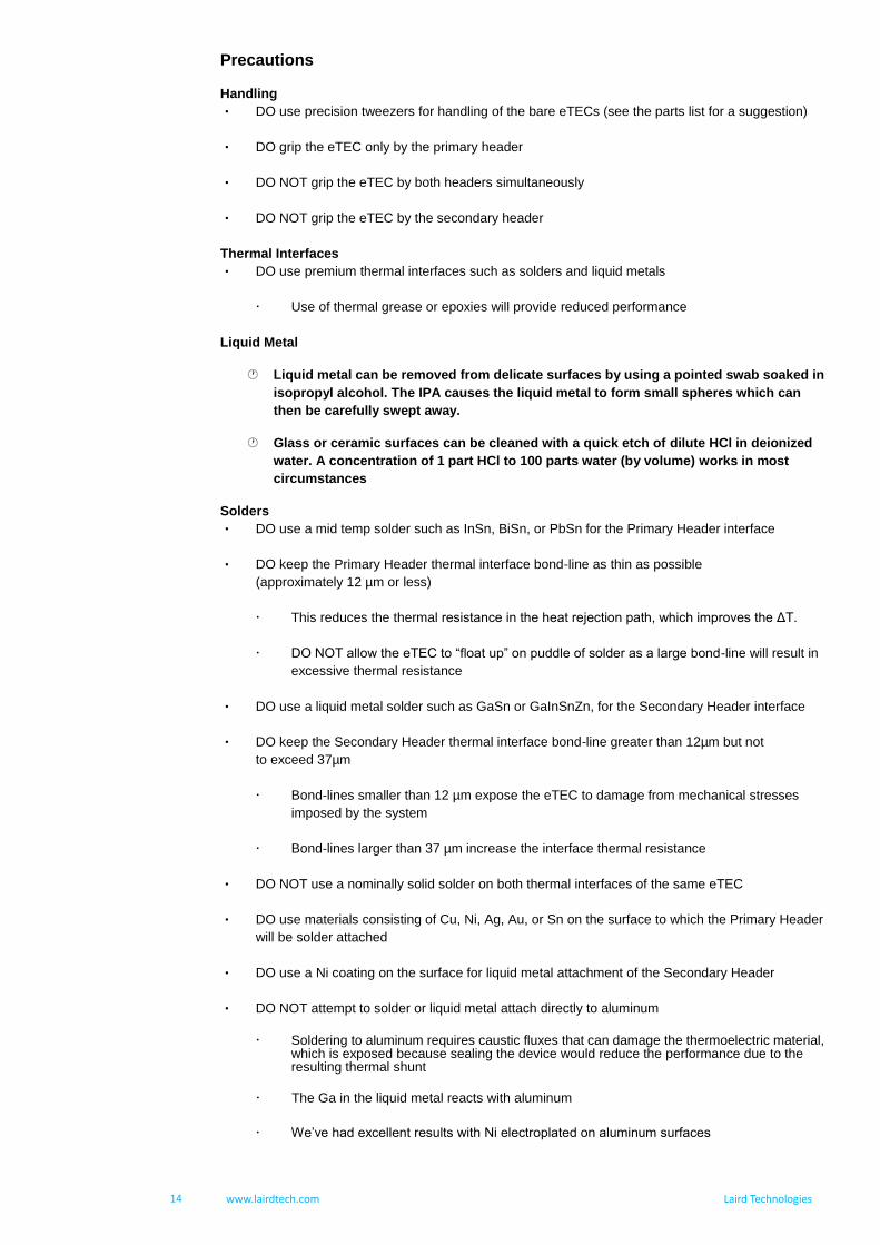
Precautions
Handling
• DO use precision tweezers for handling of the bare eTECs (see the parts list for a suggestion)
• DO grip the eTEC only by the primary header
• DO NOT grip the eTEC by both headers simultaneously
• DO NOT grip the eTEC by the secondary header
Thermal Interfaces
• DO use premium thermal interfaces such as solders and liquid metals
Use of thermal grease or epoxies will provide reduced performance
Liquid Metal
Liquid metal can be removed from delicate surfaces by using a pointed swab soaked in
isopropyl alcohol. The IPA causes the liquid metal to form small spheres which can
then be carefully swept away.
Glass or ceramic surfaces can be cleaned with a quick etch of dilute HCl in deionized
water. A concentration of 1 part HCl to 100 parts water (by volume) works in most
circumstances
Solders
• DO use a mid temp solder such as InSn, BiSn, or PbSn for the Primary Header interface
• DO keep the Primary Header thermal interface bond-line as thin as possible
(approximately 12 µm or less)
This reduces the thermal resistance in the heat rejection path, which improves the ΔT.
DO NOT allow the eTEC to ―float up‖ on puddle of solder as a large bond-line will result in
excessive thermal resistance
• DO use a liquid metal solder such as GaSn or GaInSnZn, for the Secondary Header interface
• DO keep the Secondary Header thermal interface bond-line greater than 12µm but not
to exceed 37µm
Bond-lines smaller than 12 µm expose the eTEC to damage from mechanical stresses
imposed by the system
Bond-lines larger than 37 µm increase the interface thermal resistance
• DO NOT use a nominally solid solder on both thermal interfaces of the same eTEC
• DO use materials consisting of Cu, Ni, Ag, Au, or Sn on the surface to which the Primary Header
will be solder attached
• DO use a Ni coating on the surface for liquid metal attachment of the Secondary Header
• DO NOT attempt to solder or liquid metal attach directly to aluminum
Soldering to aluminum requires caustic fluxes that can damage the thermoelectric material, which is exposed because sealing the device would reduce the performance due to the resulting thermal shunt
The Ga in the liquid metal reacts with aluminum
We’ve had excellent results with Ni electroplated on aluminum surfaces

15 www.lairdtech.com Laird Technologies
Fluxes
• DO use a mildly activated rosin flux for solder attachment of the eTEC
• DO NOT use Organic Acid or other highly reactive fluxes for eTEC attachment as immediate and
irreversible damage will occur due to its corrosive nature.
Solvents
• DO solvent clean any assembly to remove flux residues from inside the eTEC
• DO NOT leave residues of any kind inside the eTEC as it will become a thermal shunt path and
result in degraded performance.
Mechanical Supports
• DO use a mechanical support system to carry the stresses applied to the system and also to set
the bond-line of the liquid metal interface (hence mechanically decoupling the eTEC)
• DO NOT allow the eTEC to carry any mechanical load, i.e. with the system being in direct contact
with both headers at the same time
• DO use thermally resistive, rigid materials for the mechanical support (see for example the
spacers in Figure 2 above), e.g. Cirlex®
Thermal conductivity < 0.2 W/mK
Modulus > 2 GPa

16 www.lairdtech.com Laird Technologies
Temperature Sensing on Thin Film Modules
Whether you need to cool a hot spot, maintain operating temperature ranges for optimal performance
or channel heat away from sensitive electronics, thin film thermoelectric modules enable micro-scale
thermal management products for precision temperature control.
Integrated temperature sensing of the cold-side of thin film thermoelectric modules is a challenge due
to small surface area of the ceramic top substrate. Micro-scale thermistors can be mounted either
directly onto the top surface of the header or on the side of the top header to enable closed-loop
temperature control.
Temperature Sensing
The precise measurement of temperature is not always required. For some applications where thermal
boundary conditions are known, closed-loop temperature control is not required and it is adequate to
simply apply a specific current to the TEM. However, for applications that do require tight control of
temperature, it is necessary to measure the temperature on the cold side of the TEM during operation.
Thermistors have traditionally been used because they have the benefit of high temperature sensitivity
and while their resistance is non-linear with temperature, they are extremely repeatable. In addition,
thermistors have reasonably high impedance (typically 10kΏ) and are generally easier to integrate than
thermocouples. Finally, many commercially available temperature controllers include thermistor
connections making them the preferred measurement probe for closed loop feedback.
The integration of these devices onto a TE device is relatively straightforward if there is adequate
working space. Conventional thermistors tend to be on the order of 2-3 mm2. Unfortunately, this
precludes the use of these devices on thin film modules since they are as large or larger than the top
substrate. Several manufacturers have begun offering small scale thermistors that provide a pathway
to direct temperature sensing on a thin film module. Three examples of these micro-scale thermistors
are listed in Table 1 along with their size and electrical resistance.
Manufacturer Model Number L x W (mm) Resistance (k) Comments
AdSem GE-N-CHIP-103 0.1 x 0.1 10 Leadless device
BetaTHERM GR10KM3499J15 0.4 bead 10 Glass encapsulated with leads
Cornerstone Sensors T021D103 0.43 x 0.43 10 Leadless device
Table 1: Micro-scale Thermistor Products
Integration Examples
Several potential integration methods are shown below for attaching thermistors to an HV14 TEM. The
HV14 has a top header that is only 1 mm x 1.5 mm in size. Placing the thermistor on the top substrate
of the TEM is the most straightforward method of integration but uses valuable space (and limited) area
on the header.
Figure 8 shows the packaging scheme in which a laser diode was mounted on the cold side of an HV14
in a TO-8 package. Figure 9 shows a side profile of the same package. The HV14 is thermally coupled
to the chip and TO base.
Figure 8. Illustration of a laser diode TO package with embedded HV14 TEM

17 www.lairdtech.com Laird Technologies
Figure 9. Side profile of a laser diode TO package (cap removed) with embedded OptoCooler HV14 TEC and thermistor
Figure 10 illustrates placement of an AdSem thermistor to the top header of the HV14 TEC. The
AdSem is a leadless device and so the leads must be attached by the integrator.
Figure 10: HV14 with AdSem thermistor attached to top header.
Figure 11 shows the placement of a Cornerstone Sensors thermistor attached to the top header. In this
case, the ground for the thermistor is connected through the metallization of the HV14 header.
Wirebonds are used for the connection to the package posts.
Figure 11: HV14 with Cornerstone Sensors thermistor attached to top header.
18 www.lairdtech.com Laird Technologies
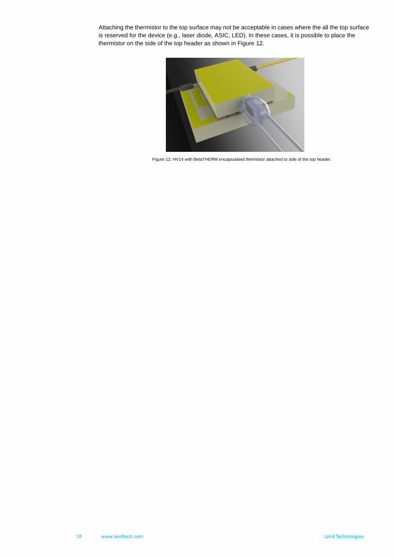
Attaching the thermistor to the top surface may not be acceptable in cases where the all the top surface
is reserved for the device (e.g., laser diode, ASIC, LED). In these cases, it is possible to place the
thermistor on the side of the top header as shown in Figure 12.
Figure 12: HV14 with BetaTHERM encapsulated thermistor attached to side of the top header.

19 www.lairdtech.com Laird Technologies
Thin Film Module Reliability Overview
The eTECTM
Series thin film thermoelectric modules have been proven to be reliable in the most
demanding applications for optoelectronic devices. Validation testing has been conducted as defined
by Telcordia’s GR468-CORE specification (see Table 2), which is the most comprehensive standard for
reliability testing of thermoelectric modules in the optoelectronic market.
Category Test Level Additional Information
Mechanical Integrity Mechanical Shock Required Condition B (1500 g, 0.5 ms), 5 times/axis
Vibration Required Condition A (20 g), 20 to 2000 to 20 Hz, 4 min/cy, 4 cy/axis
Non-Powered Environmental Stress
High Temp. Storage
Required 85°C, 2000 hr
Temperature Cycling
Required -40°C to +85°C, 500 cycles
Interim read @ 100 cycles
Powered Environmental Stress
Powered Thermal Age
Optional Tamb=85°C, 2000 hr, 5000 hr, I=Imax
Power Cycling (On/Off)
Required Hot-side T =85°C, 5000 cycles (90 sec on, 30 sec off)
Table 2: Telcordia GR468-CORE Test Protocol
Mechanical Integrity
Mechanical shock experiments were performed in accordance with MIL-STD-883E Method 2002.3 that
defines shock of 3000 g in a 0.3 ms pulse (5 times per axis)—this exceeds the requirement in GR-468
by 100%. Figure 13 shows a g-force response curve for the testing. Shock tests were performed on 12
HV14 modules, which exhibited an average change in AC resistance of -1.9% with a range of changes
from -5.8 to +3.1%. This result indicates the HV14 TEM is well within the specified range of 1500 g.
Figure 13: Shock (g-force) as a function of time showing 3000 g pulse.

20 www.lairdtech.com Laird Technologies
Non-Powered Environmental Stress
High-temperature storage provides a good indicator of long-term reliability, particularly as it relates to
diffusion-based failure modes and interface stability. The GR-468 test conditions were set at 85°C for
2000 hours. To further stress the module and accelerate temperature dependent failure mechanisms,
modules were subjected to temperatures well above the maximum operating condition of 150°C. Figure
14 shows the results of 150°C storage with read-points on the A/C resistance at 254, 432, 1190, 1526
and 2534 hours. In all cases, the A/C resistance varied less than 1% from nominal A/C resistance. This
indicates there are no temperature driven changes in the thin film material, contacts or interconnects
under these conditions and the modules are very stable.
Figure 14: Percent change in AC resistance of the HV14 modules taken at different times (hours) up to 2534 hours.
Less the 1% change in ACR was observed.
Powered Environmental Stress
Power cycling provides one of the most useful thermoelectric reliability tests as it simulates extreme
usage by inducing large current pulses that simultaneously induce large thermal gradients in the device.
These gradients produce expansion and contraction of the module that can lead to fatigue failures over
time. Conducting power cycling at elevated temperatures can also induce diffusion-based failures.
Figure 15 shows power cycling data of three HV14 modules at 90% of Imax for 100,000 cycles. In this
test, the cycle period was 5 seconds on and 5 seconds off. This rapid cycling is enabled by the fast
response time of the thin film module and enables more rapid accumulation of data. It also results in a
rapid change in the internal stress of the devices that contributes to accelerated aging and fatigue. The
∆T of the module was monitored throughout the testing and exhibited less than a 4% change over the
entire 100,000 cycle test. This far exceeded the pass/fail criteria set in GR-468 power cycling
standards.
Figure 15: Change in module ∆T over 100,000 cycles at 90% of Imax.