Embed Size (px)
Citation preview
214
Thin Film Calculator Manual
In this report, thin film model is explained. The background of thin film model is
explained at the beginning, and followed with the theory for calculating the amplitude
reflection/transmission coefficients, phase change, as well as reflectance and
transmittance. MATLAB codes are given then based on the theory, and it is used to
design a broadband reflector for the visible region of design. The results are compared
with the published data in Professor Angus Macleod’s class notes. [1] Finally, the
MATLAB codes are included in OptiScan for a user friendly interface. An example in
Thin Film Calculator in OptiScan is given to calculator the reflectance and transmittance
of Krestchmann configuration which generate surface plasma resonance at a certain
incident angle.
1. Background [1]
Optical systems consist of a series of boundaries between different materials. These
surfaces are usually optically worked so that their properties are specular, that is the
directions of light obey the laws of reflection and refraction, and their shape is adjusted to
a desired manner, such as minimizing the aberrations. Unfortunately the other properties
of the surfaces, such as reflectance, transmittance, or phase change, are rarely satisfied.
Thin films are commonly used to modify these properties without altering the specular
behavior.
215
In an optical coating, the films, together with their support, or substrate, are
generally solid. The particular materials used for the films vary with the applications. It is
possible to construct assemblies of thin films which will reduce the reflectance of a
surface and hence increase the transmittance of a component, or increase the reflectance
of a surface, or which will give high reflectance and low transmittance over part of a
region and low reflectance and high transmittance over the remainder and so on. Thin
film coatings are often known by names which describe their function, such as
antireflection coatings, beam splitters, polarizers, long-wave-pass filters, band-stop or
minus filters, or which describe their construction, such as quarter-wave stack, quarter-
half-quarter coating and so on.
In a thin-film assembly, the amount of light reflected at each interface depends on
the refractive indices of the materials on either side and thus the magnitudes of the
various beams involved in the interference can be adjusted by choosing the refractive
indices of the films. The phases of the beams on the other hand can be adjusted by
changing the layer thickness. There are thus two parameters associated with each layer,
thickness and refractive index, which can be chosen to give the required performance.
Complete freedom of choice is not possible since suitable coating materials are limited,
then the optimum theoretical performance will be also limited. Additionally there will be
inevitable drops in performance manufacture due to constructional variations.
A film in an optical coating is said to be thin when interference effects can be
detected in the light which it reflects or transmits, and thick when they cannot. Of course,
whether or not interference effects can be detected, depends as much on the source of
illumination and the receiver which is used, as on the films themselves. Even without
216
changing the wavelength, the same film can be made to appear thick or thin, depending
entirely on illumination and detection conditions. In normal coating, the films will be thin
while the substrates will be thick.
Thin film calculator is a program which is embedded in OptiScan which can be
used to calculate the amplitude reflection and transmission coefficients, phase change,
reflectance and transmittance of both s and p polarized light. The theory is briefly
explained in the following section, which is based on matching the boundary conditions
for Maxwell’s equations. Interested readers can find the detailed information in Prof.
Angus Macleod’s notes “Optical Thin Films”. [1]
2. Theory of Thin Film Model [1]
In thin film model, only linear, isotropic and homogeneous films are considered. In these
medium, the electric and magnetic fields of a harmonic wave are connected through
another material parameter, the characteristic admittance, y.
The characteristic admittance varies with wavelength but in free space it is constant. The
optical admittance of free space as is given by
217
For an arbitrary medium at given wavelength, the characteristic admittance, y, can be
written as the following.
This relationship is good through the whole of the optical region, which means for
all wavelengths shorter than several hundred microns. is the complex refractive
index for the medium. Please be carefully for the sign and convention here, since
normally is used as the complex refractive of medium. But in thin film
community, is used. In the MATLAB codes, is used as the format to
input refractive index of films. However in OptiScan, is used as the input
refractive index of films in order to be consistent with the definitions in OptiScan.
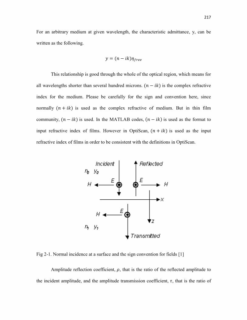
Fig 2-1. Normal incidence at a surface and the sign convention for fields [1]
Amplitude reflection coefficient, , that is the ratio of the reflected amplitude to
the incident amplitude, and the amplitude transmission coefficient, , that is the ratio of
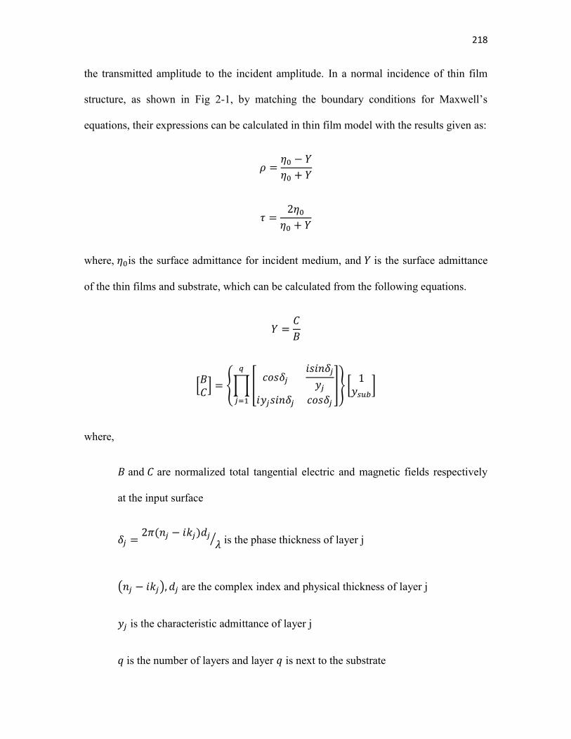
218
the transmitted amplitude to the incident amplitude. In a normal incidence of thin film
structure, as shown in Fig 2-1, by matching the boundary conditions for Maxwell’s
equations, their expressions can be calculated in thin film model with the results given as:
where, is the surface admittance for incident medium, and is the surface admittance
of the thin films and substrate, which can be calculated from the following equations.
where,
and are normalized total tangential electric and magnetic fields respectively
at the input surface
is the phase thickness of layer j
are the complex index and physical thickness of layer j
is the characteristic admittance of layer j
is the number of layers and layer is next to the substrate
219
is the characteristic admittance of the substrate
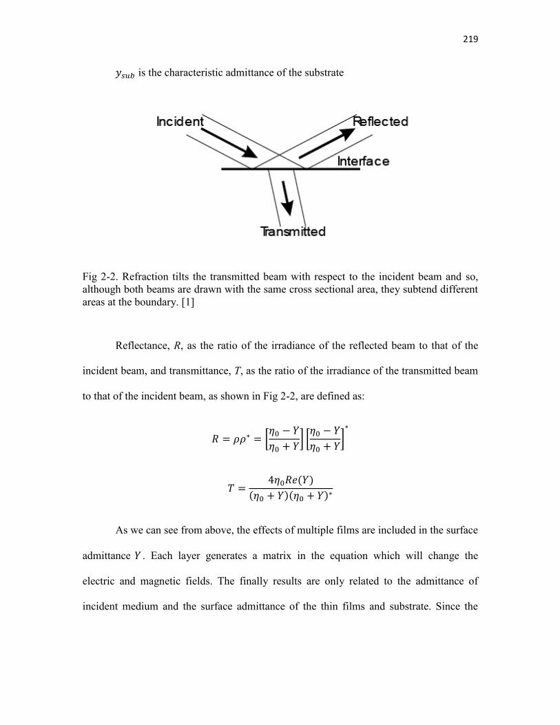
Fig 2-2. Refraction tilts the transmitted beam with respect to the incident beam and so, although both beams are drawn with the same cross sectional area, they subtend different areas at the boundary. [1]
Reflectance, R, as the ratio of the irradiance of the reflected beam to that of the
incident beam, and transmittance, T, as the ratio of the irradiance of the transmitted beam
to that of the incident beam, as shown in Fig 2-2, are defined as:
As we can see from above, the effects of multiple films are included in the surface
admittance . Each layer generates a matrix in the equation which will change the
electric and magnetic fields. The finally results are only related to the admittance of
incident medium and the surface admittance of the thin films and substrate. Since the
220
reflectance cannot be defined in an absorbing incident medium, has to be real. The
units of admittance are cancelled in the calculation.
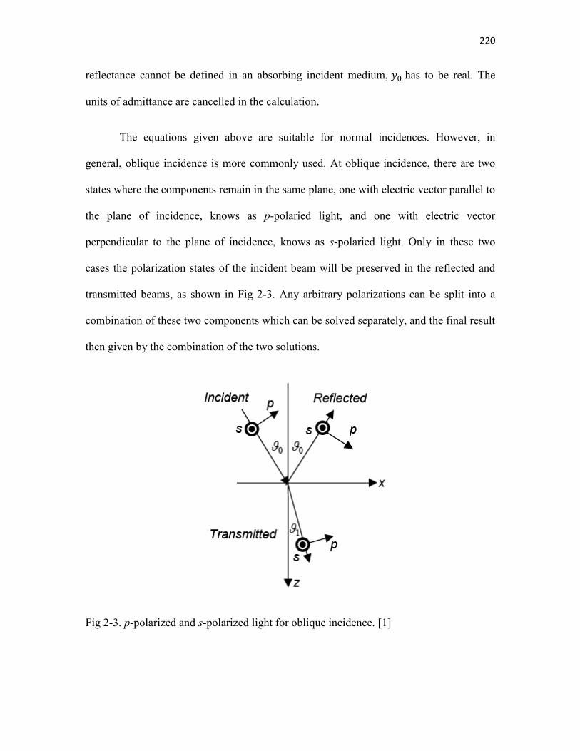
The equations given above are suitable for normal incidences. However, in
general, oblique incidence is more commonly used. At oblique incidence, there are two
states where the components remain in the same plane, one with electric vector parallel to
the plane of incidence, knows as p-polaried light, and one with electric vector
perpendicular to the plane of incidence, knows as s-polaried light. Only in these two
cases the polarization states of the incident beam will be preserved in the reflected and
transmitted beams, as shown in Fig 2-3. Any arbitrary polarizations can be split into a
combination of these two components which can be solved separately, and the final result
then given by the combination of the two solutions.
Fig 2-3. p-polarized and s-polarized light for oblique incidence. [1]
221
In thin film model, the tangential components are used to define the reflection and
transmission coefficient. This is different from the Fresnel coefficients, which uses the
total electric and magnetic fields of the waves. However, the differences are confined to
the amplitude transmission coefficient for p-polarized light.
The definitions for surface optical admittance retains as the ratio of the
components of magnetic and electric fields parallel to the interfaces but since this is
different for the two modes of polarization we need two calculations. The expressions for
amplitude reflection/transmission coefficients, reflectance and transmittance are still
valid if we replace the admittance with the tiled admittance for s-polarized and p-
polarized light.
s-polarization:
p-polarization:
Once again we emphasize that the amplitude reflection and transmittance
components are not strictly the Fresnel components. In fact, all except do coincide
with the Fresnel expressions.
222
3. MATLAB codes and examples
In this section, the MATLAB code of thin film calculator is given, as well as an example
of the broadband reflector design for the visible region. Two functions multilayer_s.m
and multilayer_p.m are built in MATLAB for different polarization incident light, and
they are the core program of thin film calculator. They calculate the amplitude
reflection/transmission coefficients, reflectance and transmittance.
The way to use these programs is shown below:
For s-polarized light:
function [rho,tao,R,T] = multilayer_s(d,y,y_inc,y_sub,lambda,theta);
For p-polarized light:
function [rho,tao,R,T] = multilayer_p(d,y,y_inc,y_sub,lambda,theta);
For arguments, multilayer_s.m and multilayer_p.m require:
d: thin film thickness (thickness for the film next to incident medium is first)
y: admittance or refractive index in the form of (admittance for the film
next to the incident medium is first)
y_inc: admittance of incident medium in the form of
y_sub: admittance of substrate in the form of
lambda: wavelength of incident light
theta: incident angle (unit in degree, can be a vector)
The outputs are:
223
rho: the complex reflection coefficient (including amplitude reflection coefficient
and phase change)
tao: the complex transmission coefficient (including amplitude transmission
coefficient and phase change)
R: reflectance
T: transmittance
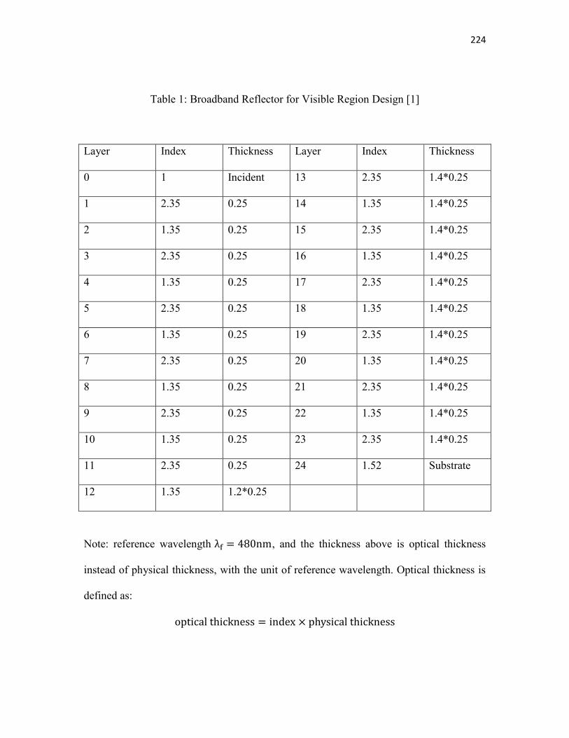
One example is provided in MATLAB code to show how to use multilayer_s.m in
the following, which is a broadband reflector for the visible region. Twenty three films
are coated on glass substrate. The reference wavelength is 480nm, two types of materials
are used for the coating with indices: 2.35 (H), and 1.35 (L). The geometry is given in the
table in the following. The thickness is given in the units of reference wavelength. And
optical thickness is used in the table instead of physical thickness for a better
understanding of the phase change of each film. The optical thickness differs from
physics thickness by a factor of index.
Optical thickness is defined as:
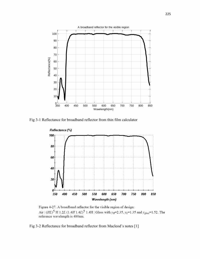
The reflectance calculated from multilayer_s.m is given in Fig 3-1, which is
compared with the published result in Macleod’s “Optical thin films”, which is given in
Fig 3-2.
224
Table 1: Broadband Reflector for Visible Region Design [1]
Layer Index Thickness Layer Index Thickness
0 1 Incident 13 2.35 1.4*0.25
1 2.35 0.25 14 1.35 1.4*0.25
2 1.35 0.25 15 2.35 1.4*0.25
3 2.35 0.25 16 1.35 1.4*0.25
4 1.35 0.25 17 2.35 1.4*0.25
5 2.35 0.25 18 1.35 1.4*0.25
6 1.35 0.25 19 2.35 1.4*0.25
7 2.35 0.25 20 1.35 1.4*0.25
8 1.35 0.25 21 2.35 1.4*0.25
9 2.35 0.25 22 1.35 1.4*0.25
10 1.35 0.25 23 2.35 1.4*0.25
11 2.35 0.25 24 1.52 Substrate
12 1.35 1.2*0.25
Note: reference wavelength , and the thickness above is optical thickness
instead of physical thickness, with the unit of reference wavelength. Optical thickness is
defined as:
225
Fig 3-1 Reflectance for broadband reflector from thin film calculator
Fig 3-2 Reflectance for broadband reflector from Macleod’s notes [1]
350 400 450 500 550 600 650 700 750 800 8500
10
20
30
40
50
60
70
80
90
100
A broadband reflector for the visible region
Wavelength(nm)
Reflecta
nce(%
)
226
3.1 thin_film_cal_example.m
% This program is an example to use thin film model. The design if a % broadband reflector for the visible region of design. % Data resource: Figure 4-27 in "Optical thin film"
% initial program
clear all; close all;
um = 1e-6; nm = 1e-9;
% define admittance for medium Air = 1; yH = 2.35; yL = 1.35; Glass = 1.52;
% define the reference wavelength and thickness lambda_f = 480*nm; dH = lambda_f/4/yH; % quarter stack dL = lambda_f/4/yL;
% define visible region of light lambda = linspace(350,850,501)*nm;
% define thin film structure y_inc = Air; % incident medium admittance y_sub = Glass; % substrate medium admittance theta = 0; % in degree d =
[dH,dL,dH,dL,dH,dL,dH,dL,dH,dL,dH,1.2*dL,1.4*dH,1.4*dL,1.4*dH,1.4*dL,... 1.4*dH,1.4*dL,1.4*dH,1.4*dL,1.4*dH,1.4*dL,1.4*dH]; y = [yH,yL,yH,yL,yH,yL,yH,yL,yH,yL,yH,yL,yH,yL,yH,yL,... yH,yL,yH,yL,yH,yL,yH];
for ii=1:length(lambda), [rho(ii),tao(ii),R(ii),T(ii)] =
multilayer_s(d,y,y_inc,y_sub,lambda(ii),theta); end
% plot the result figure, plot(lambda/nm,R*100,'-k','LineWidth',3); title('A broadband reflector for the visible region'); xlabel('Wavelength(nm)'); ylabel('Reflectance(%)'); axis([350 850 0 105]); grid on;
227
3.2 multilayer_p.m
function [rho,tao,R,T] = multilayer_p(d,y,y_inc,y_sub,lambda,theta)
% This code is for p-polarization.
for m = 1:length(theta), for i = 1:length(y), y_s(m,i) = sqrt(real(y(i))^2-imag(-y(i))^2-
y_inc^2*sind(theta(m))^2-2*1i*real(y(i))*imag(-y(i))); if imag(y_s(m,i))>0, y_s(m,i) = -(y_s(m,i)); end delta_s(m,i) = 2*pi*d(i)/lambda*y_s(m,i); y_inc_s(m) = y_inc*cosd(theta(m)); y_sub_s(m) = sqrt(real(y_sub)^2-imag(-y_sub)^2-
y_inc^2*sind(theta(m))^2-2*1i*real(y_sub)*imag(-y_sub)); if imag(y_sub_s(m))>0, y_sub_s(m) = -(y_sub_s(m)); end y_p(m,i) = y(i)^2/y_s(m,i); delta_p(m,i) = delta_s(m,i); y_inc_p(m) = y_inc^2/y_inc_s(m); y_sub_p(m) = y_sub^2/y_sub_s(m); tmp = [cos(delta_p(m,i)), 1i*sin(delta_p(m,i))/y_p(m,i); 1i*y_p(m,i)*sin(delta_p(m,i)), cos(delta_p(m,i))]; if i == 1, M = tmp; else M = M*tmp; end end BC = M*[1; y_sub_p(m)]; B(m) = BC(1); C(m) = BC(2);
% rho and tao are the amplitude reflection and transmission % coefficients rho(m) = (y_inc_p(m)*B(m)-C(m))/(y_inc_p(m)*B(m)+C(m)); phi_r(m) = angle(rho(m))/pi*180; % phase tao(m) = 2*y_inc_s(m)/(y_inc_s(m)*B(m)+C(m)); phi_t(m) = angle(tao(m))/pi*180; % phase
% R and T are the intensity reflection and transmission coefficients % Note: for transmission, the angle changes due to refraction, thus
area is % different
R(m) = abs(rho(m))^2; T(m) =
4*y_inc_p(m)*real(y_sub_p(m))/abs((y_inc_p(m)*B(m)+C(m)))^2; end
228
3.3 multilayer_s.m
function [rho,tao,R,T] = multilayer_s(d,y,y_inc,y_sub,lambda,theta)
% This code is for s-polarization.
for m = 1:length(theta), for i = 1:length(y), y_s(m,i) = sqrt(real(y(i))^2-imag(-y(i))^2-
y_inc^2*sind(theta(m))^2-2*1i*real(y(i))*imag(-y(i))); if imag(y_s(m,i))>0, y_s(m,i) = -(y_s(m,i)); end delta_s(m,i) = 2*pi*d(i)/lambda*y_s(m,i); y_inc_s(m) = y_inc*cosd(theta(m)); y_sub_s(m) = sqrt(real(y_sub)^2-imag(-y_sub)^2-
y_inc^2*sind(theta(m))^2-2*1i*real(y_sub)*imag(-y_sub)); if imag(y_sub_s(m))>0, y_sub_s(m) = -(y_sub_s(m)); end tmp = [cos(delta_s(m,i)), 1i*sin(delta_s(m,i))/y_s(m,i); 1i*y_s(m,i)*sin(delta_s(m,i)), cos(delta_s(m,i))]; if i == 1, M = tmp; else M = M*tmp; end end BC = M*[1; y_sub_s(m)]; B(m) = BC(1); C(m) = BC(2);
% rho and tao are the amplitude reflection and transmission
coefficients rho(m) = (y_inc_s(m)*B(m)-C(m))/(y_inc_s(m)*B(m)+C(m)); phi_r(m) = angle(rho(m))/pi*180; % phase tao(m) = 2*y_inc_s(m)/(y_inc_s(m)*B(m)+C(m)); phi_t(m) = angle(tao(m))/pi*180; % phase
% R and T are the intensity reflection and transmission coefficients % Note: for transmission, the angle changes due to refraction, thus
area is % different R(m) = abs(rho(m))^2; T(m) =
4*y_inc_s(m)*real(y_sub_s(m))/abs((y_inc_s(m)*B(m)+C(m)))^2; end
229
4. Thin Film Calculator in OptiScan
One example is provided in the following to show how to use Thin Film
Calculator to calculate the amplitude reflection, transmission coefficients, phase change,
reflectance and transmittance for s and p polarized light in OptiScan. The geometry is
described in the following table. A high index glass (S-LAH79) is used as the incident
medium. 45nm silver is coated on the glass to generate the surface plasma resonance, and
30nm SiO2 layer is used to protect silver from oxidation. Tested sample is located next to
SiO2 layer, and is the substrate of the geometry. The wavelength is 632.8nm.
Table 4.1: Example geometry
Material Index Thickness (nm)
Incident medium S-LAH79 1.99613 --
Metal coating Silver 0.135+3.987i 45
Protective coating SiO2 1.45708 30
Substrate Water 1.33258 --
The following are the procedures to simulate this structure in Thin Film Calculator in
OptiScan. [2]
230
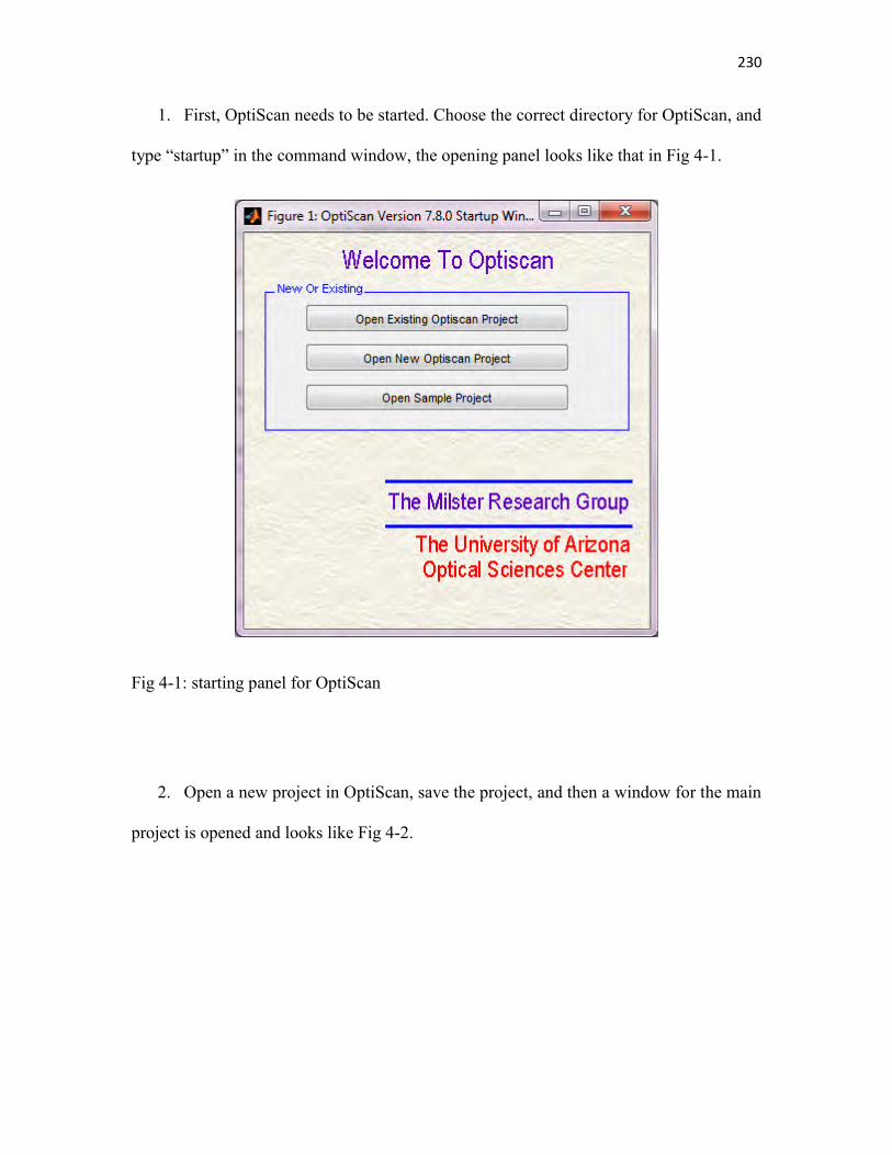
1. First, OptiScan needs to be started. Choose the correct directory for OptiScan, and
type “startup” in the command window, the opening panel looks like that in Fig 4-1.
Fig 4-1: starting panel for OptiScan
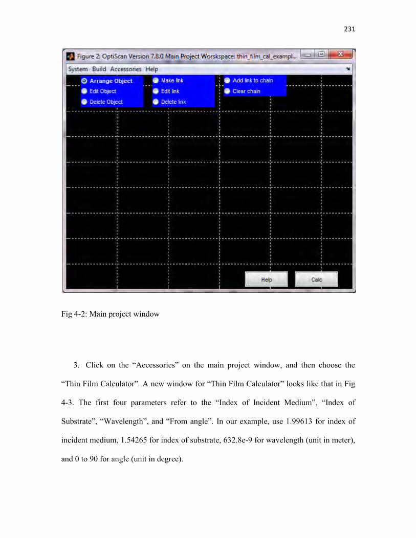
2. Open a new project in OptiScan, save the project, and then a window for the main
project is opened and looks like Fig 4-2.
231
Fig 4-2: Main project window
3. Click on the “Accessories” on the main project window, and then choose the
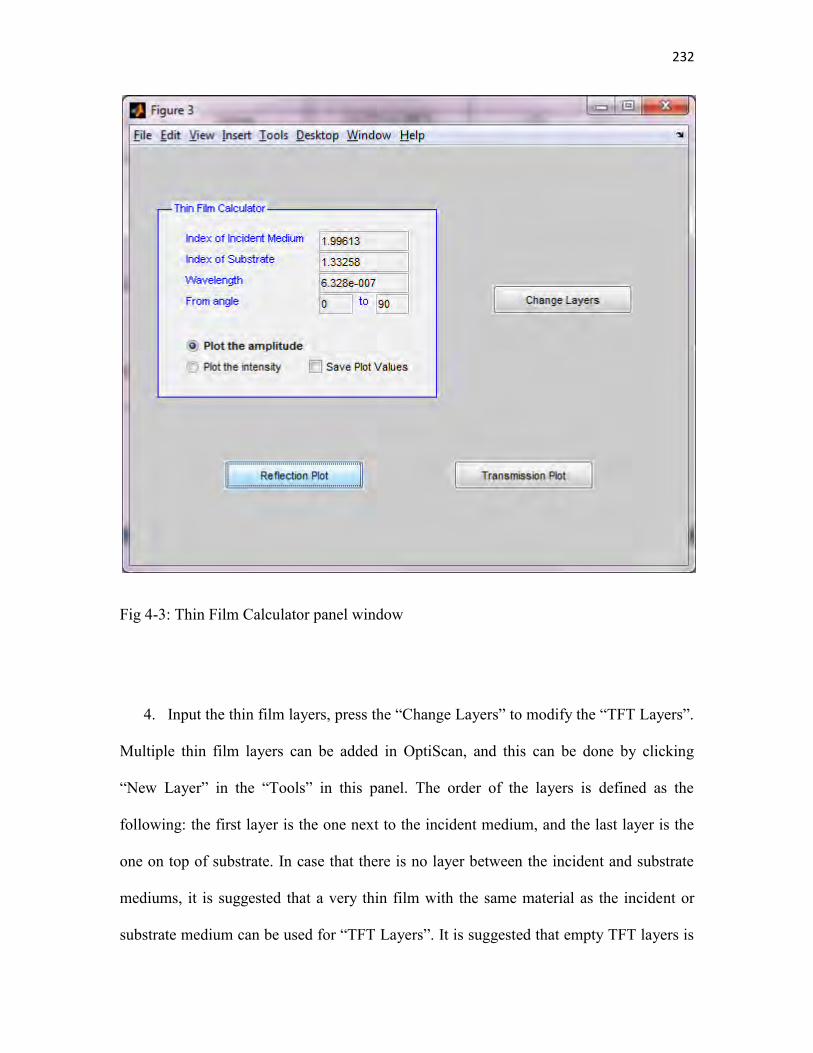
“Thin Film Calculator”. A new window for “Thin Film Calculator” looks like that in Fig
4-3. The first four parameters refer to the “Index of Incident Medium”, “Index of
Substrate”, “Wavelength”, and “From angle”. In our example, use 1.99613 for index of
incident medium, 1.54265 for index of substrate, 632.8e-9 for wavelength (unit in meter),
and 0 to 90 for angle (unit in degree).
232
Fig 4-3: Thin Film Calculator panel window
4. Input the thin film layers, press the “Change Layers” to modify the “TFT Layers”.
Multiple thin film layers can be added in OptiScan, and this can be done by clicking
“New Layer” in the “Tools” in this panel. The order of the layers is defined as the
following: the first layer is the one next to the incident medium, and the last layer is the
one on top of substrate. In case that there is no layer between the incident and substrate
mediums, it is suggested that a very thin film with the same material as the incident or
substrate medium can be used for “TFT Layers”. It is suggested that empty TFT layers is
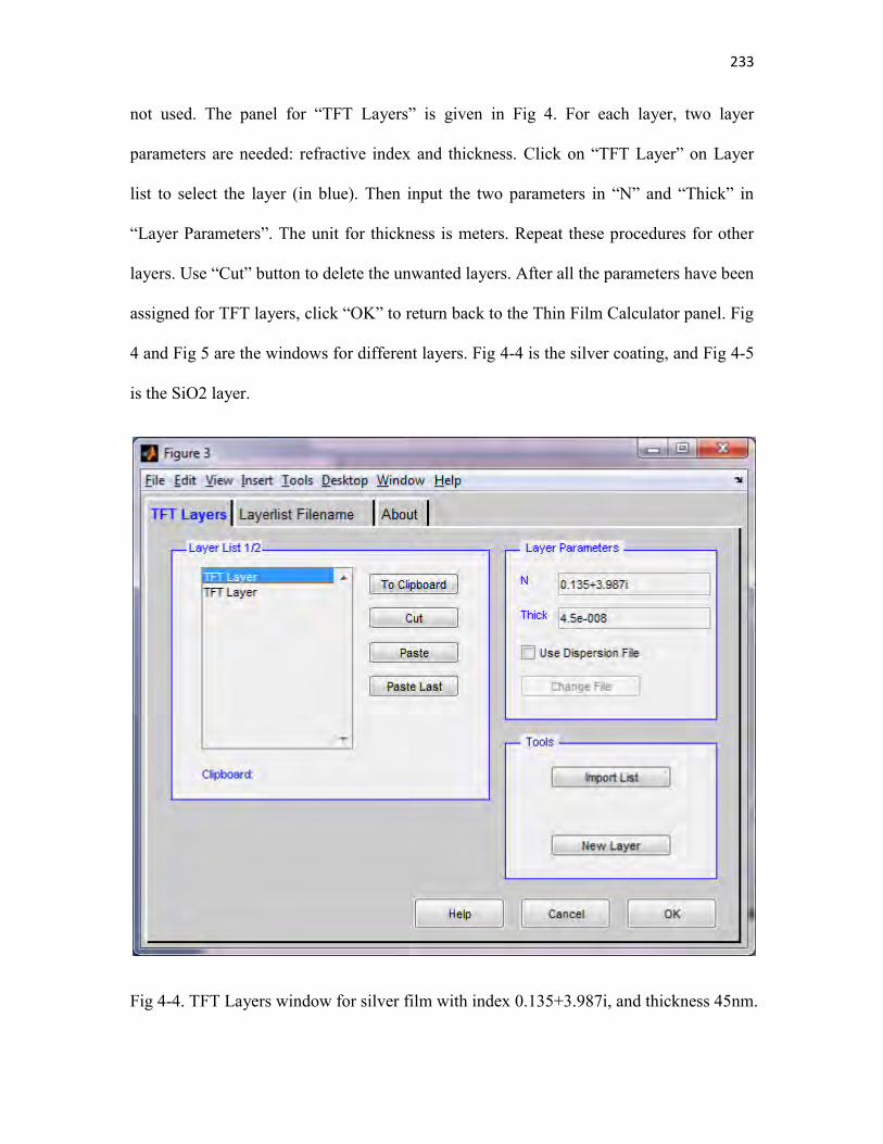
233
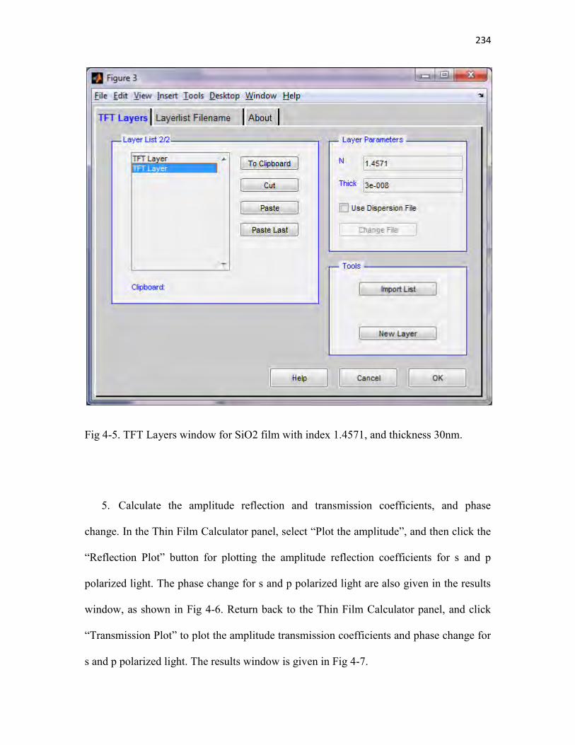
not used. The panel for “TFT Layers” is given in Fig 4. For each layer, two layer
parameters are needed: refractive index and thickness. Click on “TFT Layer” on Layer
list to select the layer (in blue). Then input the two parameters in “N” and “Thick” in
“Layer Parameters”. The unit for thickness is meters. Repeat these procedures for other
layers. Use “Cut” button to delete the unwanted layers. After all the parameters have been
assigned for TFT layers, click “OK” to return back to the Thin Film Calculator panel. Fig
4 and Fig 5 are the windows for different layers. Fig 4-4 is the silver coating, and Fig 4-5
is the SiO2 layer.
Fig 4-4. TFT Layers window for silver film with index 0.135+3.987i, and thickness 45nm.
234
Fig 4-5. TFT Layers window for SiO2 film with index 1.4571, and thickness 30nm.
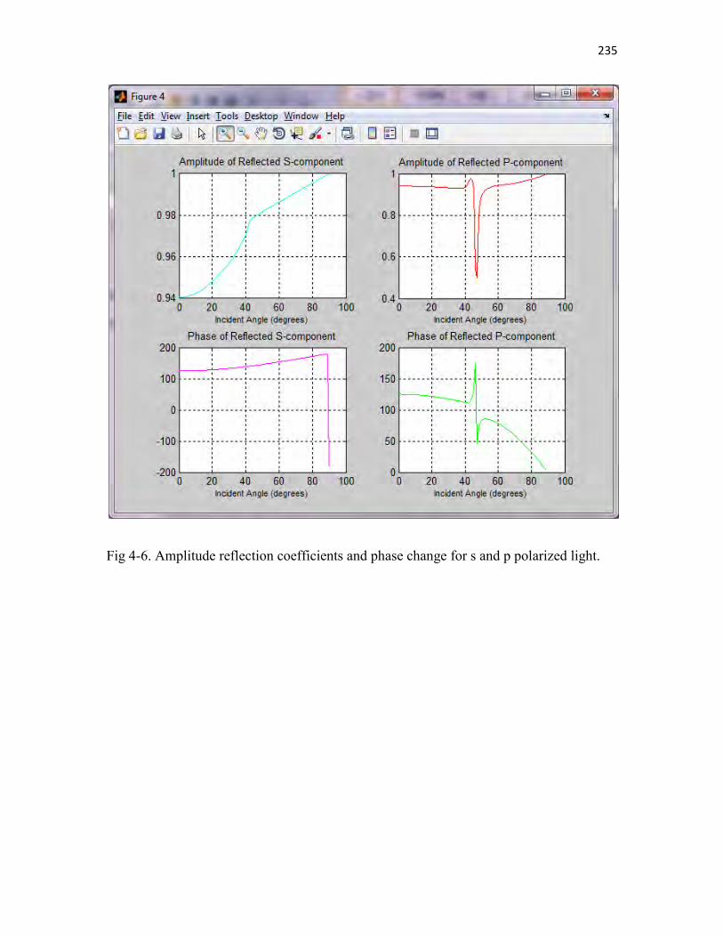
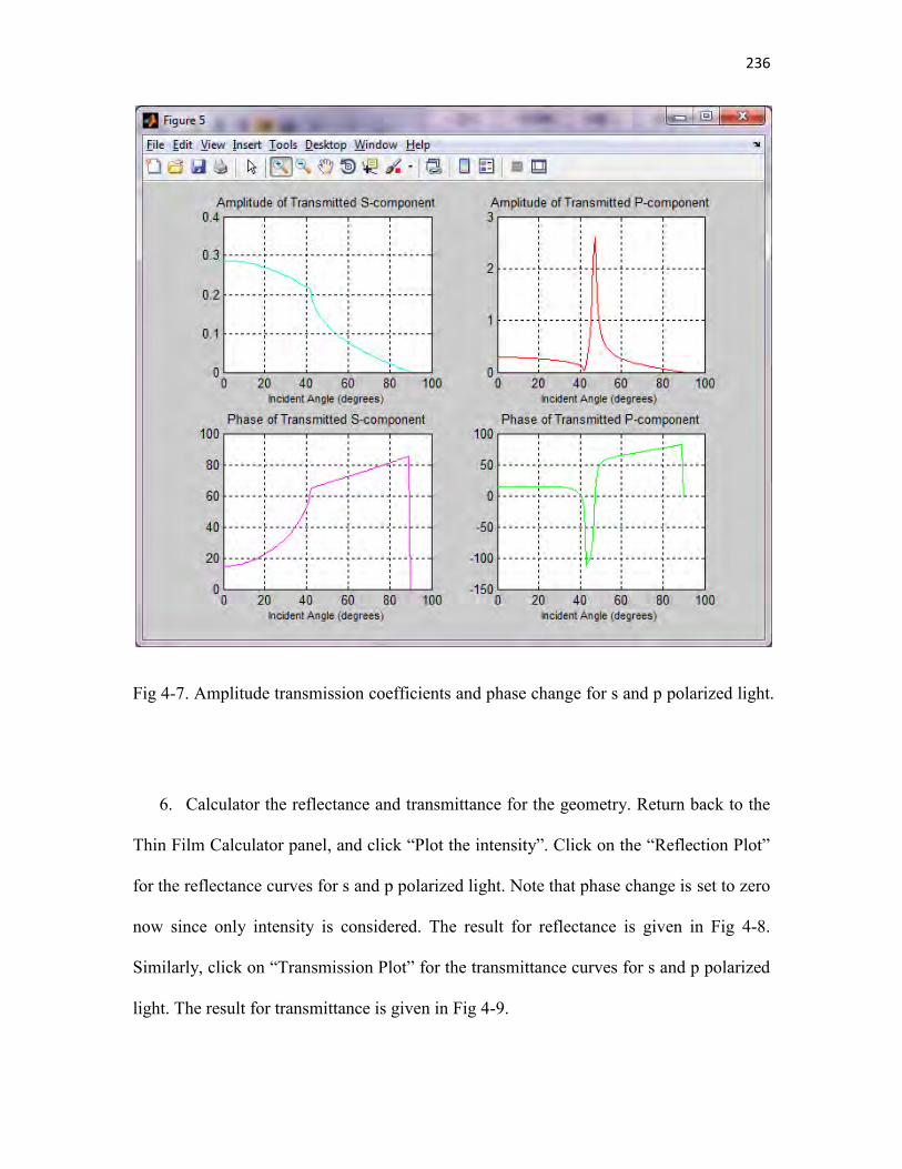
5. Calculate the amplitude reflection and transmission coefficients, and phase
change. In the Thin Film Calculator panel, select “Plot the amplitude”, and then click the
“Reflection Plot” button for plotting the amplitude reflection coefficients for s and p
polarized light. The phase change for s and p polarized light are also given in the results
window, as shown in Fig 4-6. Return back to the Thin Film Calculator panel, and click
“Transmission Plot” to plot the amplitude transmission coefficients and phase change for
s and p polarized light. The results window is given in Fig 4-7.
235
Fig 4-6. Amplitude reflection coefficients and phase change for s and p polarized light.
236
Fig 4-7. Amplitude transmission coefficients and phase change for s and p polarized light.
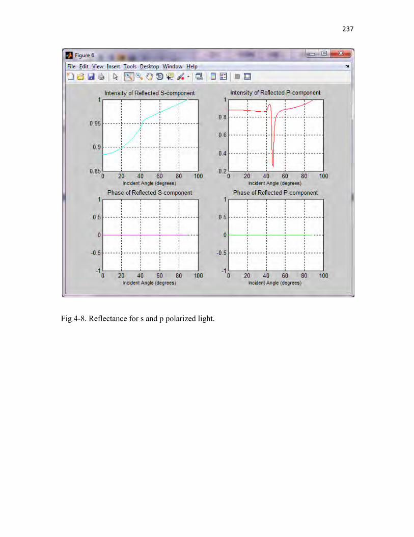
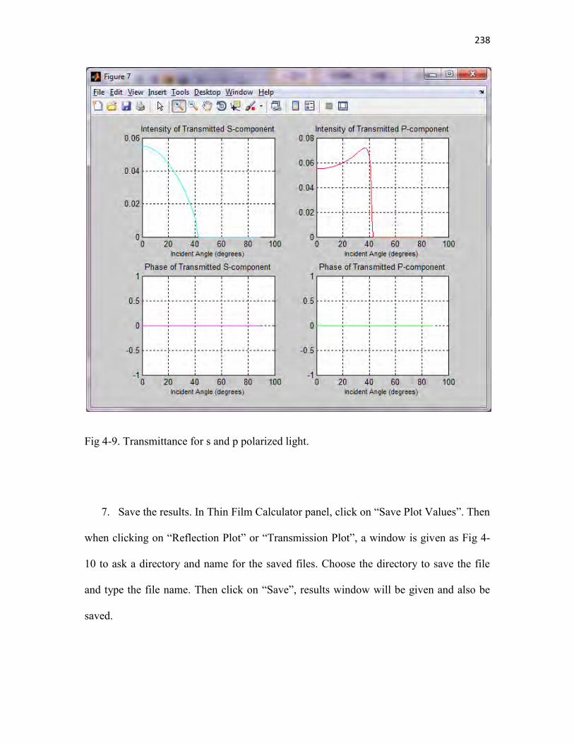
6. Calculator the reflectance and transmittance for the geometry. Return back to the
Thin Film Calculator panel, and click “Plot the intensity”. Click on the “Reflection Plot”
for the reflectance curves for s and p polarized light. Note that phase change is set to zero
now since only intensity is considered. The result for reflectance is given in Fig 4-8.
Similarly, click on “Transmission Plot” for the transmittance curves for s and p polarized
light. The result for transmittance is given in Fig 4-9.
237
Fig 4-8. Reflectance for s and p polarized light.
238
Fig 4-9. Transmittance for s and p polarized light.
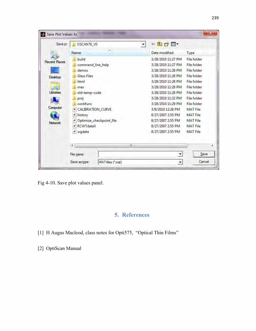
7. Save the results. In Thin Film Calculator panel, click on “Save Plot Values”. Then
when clicking on “Reflection Plot” or “Transmission Plot”, a window is given as Fig 4-
10 to ask a directory and name for the saved files. Choose the directory to save the file
and type the file name. Then click on “Save”, results window will be given and also be
saved.
239
Fig 4-10. Save plot values panel.
5. References
[1] H Augus Macleod, class notes for Opti575, “Optical Thin Films”
[2] OptiScan Manual