Embed Size (px)
Citation preview
Thermal and Electrical Effects of Staggered Micropin-Fin Dimensions for Cooling of 3D Microsystems
Thomas E. Sarvey, Yang Zhang, Yue Zhang, Hanju Oh, Muhannad S. Bakir School of Electrical and Computer Engineering
Georgia Institute of Technology
Atlanta, Georgia, USA 30318 [email protected]
ABSRACT
Microfluidic cooling shows promise in cooling next generation 3D microsystems when integrated with through-siliconvias. In this work, electrical and thermal effects of staggered micropin-fin heat sink dimensions are analyzed using deionized water. An experimental study of five different silicon micropin-fin arrays with a nominal height of 200 f.lm and diameters down to 30 f.lm was conducted at flow rates up to approximately 100 mLjmin and pressure drops up to approximately 200 kPa. The lowest convective thermal resistance achieved was 0.098 °C jW across a 1 cm2 die. These experimental results were then used to simulate temperature profiles of an interposer-cooled 3D stack.
KEYWORDS:
microfluidic cooling, 3D IC, micro pin fin, interposer
NOMENCLATURE
Rth Rcond Rconv Rheat H D PT PL Tjavg Tin Qtot k T P K
thermal resistance, °CjW conductive thermal resistance, °CjW convective thermal resistance, °CjW thermal resistance due to fluid heating, °C jW pin-fin height, f.lm pin-fin diameter, f.lm pin-fin transverse pitch, f.lm pin-fin lateral pitch, f.lm average heater temperature, °C inlet temperature, °C total heater power, W relative permittivity temperature, °C power, W thermal conductivity, W j(m 0c)
INTRODUCTION
With scaling in modem integrated circuits continuing to push power densities higher, heat dissipation has become a central barrier to continued scaling according to Moore's law. While 3D integration solves many of the problems of traditional scaling, it only exacerbates the heat dissipation problem when coupled with conventional heat sinks. Stacking device tiers under a single air cooled heat sink not only increases the thermal resistance between lower tiers and the heat sink, but also increases the total power density which must be dissipated by the heat sink. Fortunately, microfluidic cooling provides lower thermal resistances than conventional air cooled heat sinks and also scales with the number of device tiers in a 3D stack [1].
978-1-4799-5267-0114/$3l.00 © 2014 IEEE 205
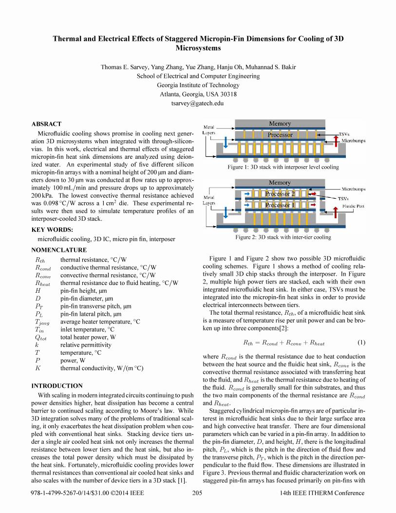
Figure 1: 3D stack with interposer level cooling
Figure 2: 3D stack with inter-tier cooling
Figure 1 and Figure 2 show two possible 3D microfluidic cooling schemes. Figure 1 shows a method of cooling relatively small 3D chip stacks through the interposer. In Figure 2, multiple high power tiers are stacked, each with their own integrated microfluidic heat sink. In either case, TSVs must be integrated into the micropin-fin heat sinks in order to provide electrical interconnects between tiers.
The total thermal resistance, Rth' of a microfluidic heat sink is a measure of temperature rise per unit power and can be broken up into three components[2]:
Rth = Rcond + Rconv + Rheat (1)
where Rcond is the thermal resistance due to heat conduction between the heat source and the fluidic heat sink, Rconv is the convective thermal resistance associated with transferring heat to the fluid, and Rheat is the thermal resistance due to heating of the fluid. Rcond is generally small for thin substrates, and thus the two main components of the thermal resistance are Rcond and Rheat.
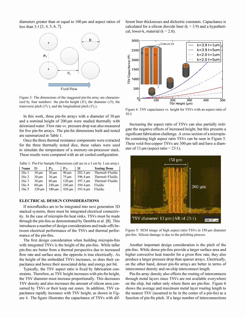
Staggered cy lindrical micropin-fin arrays are of particular interest in microfluidic heat sinks due to their large surface area and high convective heat transfer. There are four dimensional parameters which can be varied in a pin-fin array. In addition to the pin-fin diameter, D, and height, H, there is the longitudinal pitch, PL, which is the pitch in the direction of fluid flow and the transverse pitch, PT, which is the pitch in the direction perpendicular to the fluid flow. These dimensions are illustrated in Figure 3. Previous thermal and fluidic characterization work on staggered pin-fin arrays has focused primarily on pin-fins with
14th IEEE ITHERM Conference
diameters greater than or equal to 100 f.!m and aspect ratios of less than 3:1 [3, 4, 5, 6, 7].
o Fluid Flow
Figure 3: The dimensions of the staggered pin-fin array are character
ized by four numbers: the pin-fin height (H), the diameter (D), the
transverse pitch (FT), and the longitudinal pitch (FL).
In this work, three pin-fin arrays with a diameter of 30 f.!m and a nominal height of 200 f.!m were studied thermally with deionized water. Flow rate vs. pressure drop was also measured for five pin-fin arrays. The pin-fin dimensions built and tested are summarized in Table 1.
Once the three thermal resistance components were extracted for the three thermally tested dice, these values were used to simulate the temperature of a memory-on-processor stack. These results were compared with an air cooled configuration.
Table 1: Pin-Fin Sample Dimensions (all are in a 1 cm by 1 cm array)
Name D PL PT H Testing Done Die 1 30�m 30 J.II11 90�m 202.1 �m Thermal+Fluidic Die 2 30�m 36J.1111 75 �m 196.4 �m Thermal+Fluidic Die 3 30�m 60J.ll11 120 J.II11 197.1 �m Thermal+Fluidic Die 4 60J.ll11 240J.ll11 240J.ll11 194.4�m Fluidic DieS l20�m l80J.ll11 420J.ll11 193.6�m Fluidic
ELECTRICAL DESIGN CONSIDERATIONS
If microfluidics are to be integrated into next generation 3D stacked systems, there must be integrated electrical connectivity. In the case of micro pin-fin heat sinks, TSVs must be made through the pin-fins as demonstrated by Dembla et al. [8]. This introduces a number of design considerations and trade-offs between electrical performance of the TSVs and thermal performance of the pin-fins.
The first design consideration when building micropin-fins with integrated TSVs is the height of the pin-fins. While taller pin-fins are better from a thermal perspective due to increased flow rate and surface area, the opposite is true electrically. As the height of the embedded TSVs increases, so does their capacitance and hence their associated delay and energy per bit.
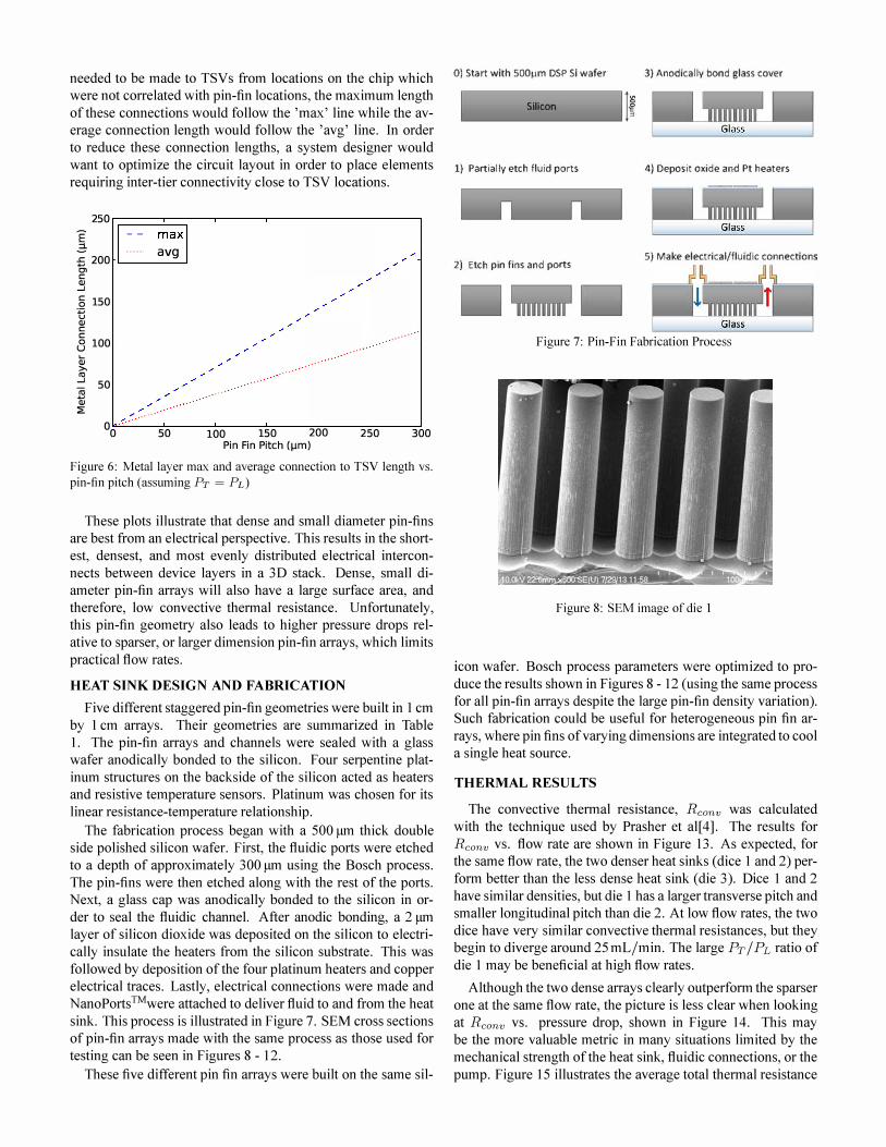
Typically, the TSV aspect ratio is fixed by fabrication constraints. Therefore, as TSV height increases with pin-fin height, the TSV diameter must increase proportionally. This decreases TSV density and also increases the amount of silicon area consumed by TSVs or their keep out zones. In addition, TSV capacitance rapidly increases with TSV height, as shown in Figure 4. The figure illustrates the capacitance of TSVs with dif-
ferent liner thicknesses and dielectric constants. Capacitance is calculated for a silicon dioxide liner (k = 3.9) and a hypothetical, lower-k, material (k = 2.0).
-u.e.e.:mic (kl �SP.�
100 200 300 TSV Height (!Jm)
k=3.9 t=lum k=3.9 t=5um k=2.0 t=lum k=2.0 t=5um
. '
400 500
Figure 4: TSV capacitance vs. height for TSVs with an aspect ratio of
10: 1
Increasing the aspect ratio of TSVs can also partially mitigate the negative effects of increased height, but this presents a significant fabrication challenge. A cross section of a micropinfin containing high aspect ratio TSVs can be seen in Figure 5. These void-free copper TSVs are 300 f.!m tall and have a diameter of 13 f.!m (aspect ratio = 23:1).
Figure 5: SEM image of high aspect ratio TSVs in 150 /lm diameter
pin-fins. Silicon damage is due to the polishing process.
Another important design consideration is the pitch of the pin-fins. While dense pin-fins provide a larger surface area and higher convective heat transfer for a given flow rate, they also produce a larger pressure drop than sparser arrays. Electrically, on the other hand, denser pin-fin arrays are better in terms of interconnect density and on-chip interconnect length.
Pin-fin array density also effects the routing of interconnects through metal layers since TSVs are not available everywhere on the chip, but rather only where there are pin-fins. Figure 6 shows the average and maximum metal layer routing length to the nearest TSV (assumed to be in the center of a pin-fin) as a function of pin-fin pitch. If a large number of interconnections
needed to be made to TSVs from locations on the chip which were not correlated with pin-fin locations, the maximum length of these connections would follow the 'max' line while the average connection length would follow the 'avg' line. In order to reduce these connection lengths, a system designer would want to optimize the circuit layout in order to place elements requiring inter-tier connectivity close to TSV locations.
250
E 2-£ 200 Cl C a! ....J c 150 0
:;::; u a! C C 0 100 u L-a! :>. m ....J
50 iii ...., a! ::E
00
� ...... avg
, . ' «, . ,
50
.....
100 150 200 Pin Fin Pitch (!Jm)
.......
....
250 300
Figure 6: Metal layer max and average connection to TSV length vs.
pin-fin pitch (assuming PT = PL)
These plots illustrate that dense and small diameter pin-fins are best from an electrical perspective. This results in the shortest, densest, and most evenly distributed electrical interconnects between device layers in a 3D stack. Dense, small diameter pin-fin arrays will also have a large surface area, and therefore, low convective thermal resistance. Unfortunately, this pin-fin geometry also leads to higher pressure drops relative to sparser, or larger dimension pin-fin arrays, which limits practical flow rates.
HEAT SINK DESIGN AND FABRICATION
Five different staggered pin-fin geometries were built in 1 cm by 1 cm arrays. Their geometries are summarized in Table 1. The pin-fin arrays and channels were sealed with a glass wafer anodically bonded to the silicon. Four serpentine platinum structures on the backside of the silicon acted as heaters and resistive temperature sensors. Platinum was chosen for its linear resistance-temperature relationship.
The fabrication process began with a 500 11m thick double side polished silicon wafer. First, the fluidic ports were etched to a depth of approximately 300 11m using the Bosch process. The pin-fins were then etched along with the rest of the ports. Next, a glass cap was anodically bonded to the silicon in order to seal the fluidic channel. After anodic bonding, a 211m layer of silicon dioxide was deposited on the silicon to electrically insulate the heaters from the silicon substrate. This was followed by deposition of the four platinum heaters and copper electrical traces. Lastly, electrical connections were made and NanoPorts TMwere attached to deliver fluid to and from the heat sink. This process is illustrated in Figure 7. SEM cross sections of pin-fin arrays made with the same process as those used for testing can be seen in Figures 8 - 12.
These five different pin fin arrays were built on the same sil-
0) Start with 500pm DSP Si wafer 3) Anodically bond glass cover
i �----------------� Silicon
1) Partially etch fluid ports 4) Deposit oxide and Pt heaters
2) Etch pin fins and ports 5) Make electrical/fluidic connections
Figure 7: Pin-Fin Fabrication Process
Figure 8: SEM image of die 1
icon wafer. Bosch process parameters were optimized to produce the results shown in Figures 8 - 12 (using the same process for all pin-fin arrays despite the large pin-fin density variation). Such fabrication could be useful for heterogeneous pin fin arrays, where pin fins of varying dimensions are integrated to cool a single heat source.
THERMAL RESULTS
The convective thermal resistance, Rconv was calculated with the technique used by Prasher et al[4]. The results for Rconv vs. flow rate are shown in Figure 13. As expected, for the same flow rate, the two denser heat sinks (dice 1 and 2) perform better than the less dense heat sink (die 3). Dice 1 and 2 have similar densities, but die 1 has a larger transverse pitch and smaller longitudinal pitch than die 2. At low flow rates, the two dice have very similar convective thermal resistances, but they begin to diverge around 25 mL/min. The large PT / PL ratio of die 1 may be beneficial at high flow rates.
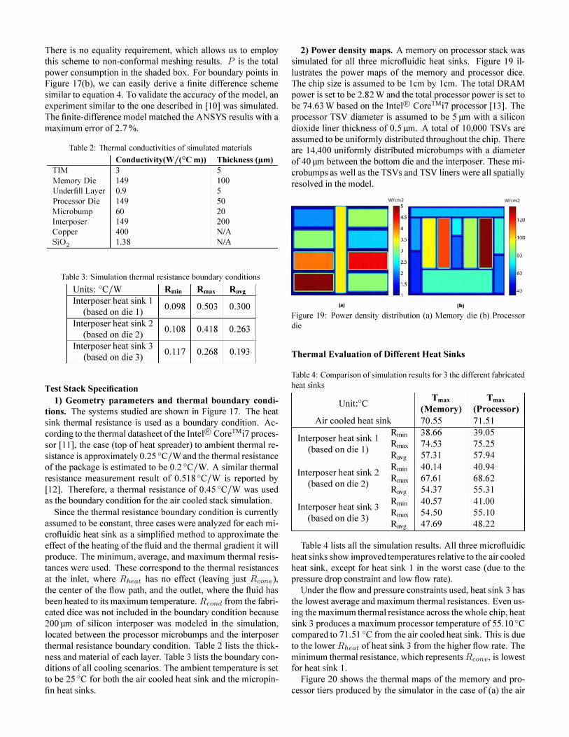
Although the two dense arrays clearly outperform the sparser one at the same flow rate, the picture is less clear when looking at Rconv vs. pressure drop, shown in Figure 14. This may be the more valuable metric in many situations limited by the mechanical strength of the heat sink, fluidic connections, or the pump. Figure 15 illustrates the average total thermal resistance
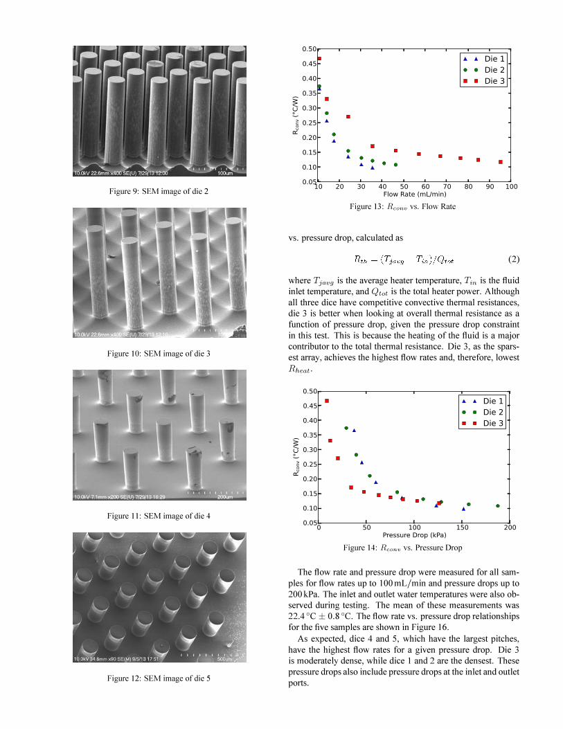
Figure 9: SEM image of die 2
Figure 10: SEM image of die 3
Figure 1 1: SEM image of die 4
Figure 12: SEM image of die 5
Figure 13: Rconv vs. Flow Rate
vs. pressure drop, calculated as
(2)
where Tjavg is the average heater temperature, Tin is the fluid inlet temperature, and Qtot is the total heater power. Although all three dice have competitive convective thermal resistances, die 3 is better when looking at overall thermal resistance as a function of pressure drop, given the pressure drop constraint in this test. This is because the heating of the fluid is a major contributor to the total thermal resistance. Die 3, as the sparsest array, achieves the highest flow rates and, therefore, lowest Rheat.
Figure 14: Rconv vs. Pressure Drop
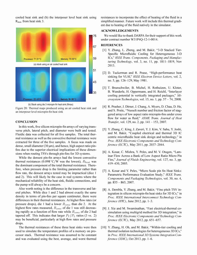
The flow rate and pressure drop were measured for all samples for flow rates up to 100 mL/min and pressure drops up to 200 kPa. The inlet and outlet water temperatures were also observed during testing. The mean of these measurements was 22.4 °C ± 0.8 0c. The flow rate vs. pressure drop relationships for the five samples are shown in Figure 16.
As expected, dice 4 and 5, which have the largest pitches, have the highest flow rates for a given pressure drop. Die 3 is moderately dense, while dice 1 and 2 are the densest. These pressure drops also include pressure drops at the inlet and outlet ports.
10 20 30 40 50 60 70 80 90 100Flow Rate (mL/min)
0.05
0.10
0.15
0.20
0.25
0.30
0.35
0.40
0.45
0.50
R con
v (°C
/W)
Die 1Die 2Die 3
0 50 100 150 200Pressure Drop (kPa)
0.05
0.10
0.15
0.20
0.25
0.30
0.35
0.40
0.45
0.50
R con
v (°C
/W)
Die 1Die 2Die 3
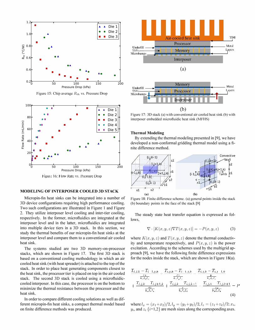
Figure 15: Chip average Rth vs. Pressure Drop
MODELING OF INTERPOSER COOLED 3D STACK
Micropin-fin heat sinks can be integrated into a number of 3D device configurations requiring high performance cooling. Two such configurations are illustrated in Figure 1 and Figure 2. They utilize interposer level cooling and inter-tier cooling, respectively. In the former, microfluidics are integrated at the interposer level and in the latter, microfluidics are integrated into mUltiple device tiers in a 3D stack. In this section, we study the thermal benefits of our micropin-fin heat sinks at the interposer level and compare them to a conventional air cooled heat sink.
The systems studied are two 3D memory-on-processor stacks, which are shown in Figure 17. The first 3D stack is based on a conventional cooling methodology in which an air cooled heat sink (with heat spreader) is attached to the top of the stack. In order to place heat generating components closest to the heat sink, the processor tier is placed on top in the air cooled stack. The second 3D stack is cooled using a microfluidiccooled interposer. In this case, the processor is on the bottom to minimize the thermal resistance between the processor and the heat sink.
In order to compare different cooling solutions as well as different micropin-fin heat sinks, a compact thermal model based on finite difference methods was produced.
Processor • Memory
Interposer
(a)
"111111111� ____ "_IIIIIIIIIIIIIIIIIIIII��" ___ Metal Layers
����----------��._��I
(b) Figure 17: 3D stack (a) with conventional air cooled heat sink (b) with
interposer embedded microfluidic heat sink (MFHS)
Thermal Modeling
By extending the thermal modeling presented in [9], we have developed a non-conformal gridding thermal model using a finite difference method.
(a) (b)
Convective �all
' , j +1,k) }2 ·:.o+"'+.-'-'-::T"':'a m b Iz 1
Figure 18: Finite difference scheme. (a) general points inside the stack
(b) boundary points in the face of the stack [9]
The steady state heat transfer equation is expressed as follows,
'9. [K(x,y,z)'9T(x,y,z)] = -P(x,y,z) (3)
where K(x, y, z) and T(x, y, z) denote the thermal conductivity and temperature respectively, and P(x, y, z) is the power excitation. According to the schemes used by the multigrid approach [9], we have the following finite difference expressions for the nodes inside the stack, which are shown in Figure 18(a).
(4)
where lx = (Xl +X2)/2, ly = (Yl +Y2)/2, lz = (Zl +Z2)/2; Xi, Yi, and Zi {i= 1 ,2} are mesh sizes along the corresponding axes.
0 50 100 150 200Pressure Drop (kPa)
0.2
0.4
0.6
0.8
1.0
1.2R t
h (°C
/W)
Die 1Die 2Die 3
0 50 100 150 200Pressure Drop (kPa)
0
20
40
60
80
100
Flow
Rate (m
L/min)
Die 1Die 2Die 3Die 4Die 5
There is no equality requirement, which allows us to employ this scheme to non-conformal meshing results. P is the total power consumption in the shaded box. For boundary points in Figure 17(b), we can easily derive a finite difference scheme similar to equation 4. To validate the accuracy of the model, an experiment similar to the one described in [10] was simulated. The finite-difference model matched the ANSYS results with a maximum error of 2.7 %.
Table 2: Thermal conductivities of simulated materials
Conductivity(W leC m» Thickness (/-lm) TIM 3 5 Memory Die 149 100 Underfill Layer 0.9 5 Processor Die 149 50 Microbump 60 20 Interposer 149 200 Copper 400 N/A Si02 1.38 N/A
Table 3: Simulation thermal resistance boundary conditions
Units: °C/W Rmin Rmax Ravg Interposer heat sink 1
0.098 0.503 0.300 (based on die 1)
Interposer heat sink 2 0.108 0.418 0.263
(based on die 2) Interposer heat sink 3
0.117 0.268 0.193 (based on die 3)
Test Stack Specification
1) Geometry parameters and thermal boundary condi
tions. The systems studied are shown in Figure 17. The heat sink thennal resistance is used as a boundary condition. According to the thermal datasheet of the Intel® Core™i7 processor [11], the case (top of heat spreader) to ambient thermal resistance is approximately 0.25 °C/W and the thermal resistance of the package is estimated to be 0.2 °C/W. A similar thennal resistance measurement result of 0.518 °C/W is reported by [12]. Therefore, a thermal resistance of 0.45 °C/W was used as the boundary condition for the air cooled stack simulation.
Since the thermal resistance boundary condition is currently assumed to be constant, three cases were analyzed for each microfluidic heat sink as a simplified method to approximate the effect of the heating of the fluid and the thennal gradient it will produce. The minimum, average, and maximum thennal resistances were used. These correspond to the thermal resistances at the inlet, where Rheat has no effect (leaving just Rconv), the center of the flow path, and the outlet, where the fluid has been heated to its maximum temperature. Rcond from the fabricated dice was not included in the boundary condition because 200 f.!m of silicon interposer was modeled in the simulation, located between the processor microbumps and the interposer thermal resistance boundary condition. Table 2 lists the thickness and material of each layer. Table 3 lists the boundary conditions of all cooling scenarios. The ambient temperature is set to be 25 °C for both the air cooled heat sink and the micropinfin heat sinks.
2) Power density maps. A memory on processor stack was simulated for all three microfluidic heat sinks. Figure 19 illustrates the power maps of the memory and processor dice. The chip size is assumed to be lcm by lcm. The total DRAM power is set to be 2.82 W and the total processor power is set to be 74.63 W based on the Intel® Core™i7 processor [13]. The processor TSV diameter is assumed to be 5 f.!m with a silicon dioxide liner thickness of 0.5 f.!m. A total of 10,000 TSVs are assumed to be uniformly distributed throughout the chip. There are 14,400 unifonnly distributed microbumps with a diameter of 40 f.!m between the bottom die and the interposer. These microbumps as well as the TSVs and TSV liners were all spatially resolved in the model.
W/cm2 Wlcm2
10) (b) Figure 19: Power density distribution (a) Memory die (b) Processor
die
Thermal Evaluation of Different Heat Sinks
Table 4: Comparison of simulation results for 3 the different fabricated
heat sinks
UnieC Tmax Tmax (Memory) (Processor)
Air cooled heat sink 70.55 71.51
Interposer heat sink 1 Rmin 38.66 39.05 Rmax 74.53 75.25
(based on die 1) Ravg 57.31 57.94
Interposer heat sink 2 Rmin 40.l4 40.94 Rmax 67.61 68.62
(based on die 2) Ravg 54.37 55.31
Interposer heat sink 3 Rmin 40.57 41.00 Rmax 54.50 55.10
(based on die 3) Ravg 47.69 48.22
Table 4 lists all the simulation results. All three microfluidic heat sinks show improved temperatures relative to the air cooled heat sink, except for heat sink 1 in the worst case (due to the pressure drop constraint and low flow rate).
Under the flow and pressure constraints used, heat sink 3 has the lowest average and maximum thermal resistances. Even using the maximum thennal resistance across the whole chip, heat sink 3 produces a maximum processor temperature of 55.10 °C compared to 71.51 °C from the air cooled heat sink. This is due to the lower Rheat of heat sink 3 from the higher flow rate. The minimum thermal resistance, which represents Rconv, is lowest for heat sink 1.
Figure 20 shows the thennal maps of the memory and processor tiers produced by the simulator in the case of (a) the air
cooled heat sink and (b) the interposer level heat sink using Rmax from heat sink 3.
resistances to incorporate the effect of heating of the fluid in a simplified manner. Future work will include this thermal gradient due to heating of the fluid natively in the simulator.
ACKNOWLEDGEMENTS
75 We would like to thank DARPA for their support of this work
67
Processor; 71.51 °C Memory; 70.55°C 59
(a) stack using an air cooled heat sink
(b) Stack using die 3 micropin-fin heat sink (Rmax) Figure 20: Thermal maps produced using an air cooled heat sink and
an interposer level micropin-fin heat sink
CONCLUSION
In this work, five silicon micropin-fin arrays of varying transverse pitch, lateral pitch, and diameter were built and tested. Fluidic data was collected for all five samples. The total thermal resistance as well as the convective thermal resistance were extracted for three of the five samples. A focus was made on dense, small diameter (30 /lm), and hence, high aspect ratio pinfins due to the superior electrical implications of these dimensions when routing TSVs through pin-fins for 3D systems.
While the densest pin-fin arrays had the lowest convective thermal resistances (0.098 °CjW was the lowest), Rheat was the dominant component of the total thermal resistance. Therefore, when pressure drop is the limiting parameter rather than flow rate, the densest arrays tested may be impractical (dice I and 2). This will likely be the case in real systems where the mechanical reliability of the heat sink, fluidic connections, and the pump will always be a concern.
Also worth noting is the difference in the transverse and lateral pitches. While dice 1 and 2 had almost exactly the same density in terms of pin-fins per square centimeter, there were differences in their thermal resistances. At higher flow rates (or pressure drops), die 1 had a lower Rconv than die 2. At the highest flow rates measured, Rconv of die 1 was still decreasing rapidly as a function of flow rate while Rconv of die 2 had tapered off. This indicates that larger PT j PL ratios (3 vs. 2) may be beneficial, particularly at high flow rates and pressure drops.
The thermal resistances of these three heat sinks were then used to simulate the temperature profiles of a memory on processor stack. Thermal resistance was assumed to be constant and was evaluated using the best, average, and worst thermal
under contract number W31P4Q-12-1-0014.
REFERENCES
[1] Y. Zhang, L. Zheng, and M. Bakir, "3-D Stacked TierSpecific Microfluidic Cooling for Heterogeneous 3-D ICs, " IEEE Trans. Components, Packaging and Manufac
turing Technology, vol. 3, no. 11, pp. 1811-1819, Nov 2013.
[2] D. Tuckerman and R. Pease, "High-performance heat sinking for VLSI, " IEEE Electron Device Letters, vol. 2, no. 5, pp. 126-129, May 1981.
[3] T. Brunschwiler, B. Michel, H. Rothuizen, U. Kloter, B. Wunderle, H. Oppermann, and H. Reichl, "Interlayer cooling potential in vertically integrated packages, " Mi
crosystem Technologies, vol. 15, no. 1, pp. 57 - 74, 2008.
[4] R. Prasher, J. Dirner, J. Chang, A. Myers, D. Chau, D. He, and S. Prstic, "Nusselt number and friction factor of staggered arrays of low aspect ratio micropin-fins under cross flow for water as fluid, " ASME Trans. Journal of Heat
Transfer, vol. 129, no. 2, pp. 141 - 153, 2007.
[5] Y. Zhang, C. King, J. Zaveri, Y. J. Kim, V. Sahu, Y. Joshi, and M. Bakir, "Coupled electrical and thermal 3D IC centric microfluidic heat sink design and technology, " in Proc. IEEE Electronic Components and Technology Con
ference (ECTC), May 2011, pp. 2037-2044.
[6] A. Kosar, C. Mishra, Y. Peles, and M. V. Otugen, "Laminar Flow Across a Bank of Low Aspect Ratio Micro Pin Fins, " Journal of Fluids Engineering, vol. 127, no. 3, pp. 419-430, 2005.
[7] A. Kosar and Y. Peles, "Micro Scale pin fin Heat Sinks: Parametric Performance Evaluation Study, " IEEE Trans.
Components and Packaging Technologies, vol. 30, no. 4, pp. 855 - 865, 2007.
[8] A. Dembla, Y. Zhang, and M. Bakir, "Fine pitch TSV integration in silicon micropin-fin heat sinks for 3D ICs, " in Proc. IEEE International Interconnect Technology Con
ference (llTC), June 2012, pp. 1-3.
[9] J. Xie and M. Swaminathan, "Fast electrical-thermal cosimulation using multigrid method for 3D integration, " in Proc. IEEE Electronic Components and Technology Con
ference (ECTC), May 2012, pp. 651-657.
[10] Y. Zhang, H. Oh, and M. Bakir, "Within-tier cooling and thermal isolation technologies for heterogeneous 3D ICs, " in Proc. IEEE International 3D Systems Integration Con
ference (3DIC), Oct 2013, pp. 1-6.

[11] Intel, Intel® Core™i7 Processor Families for the
LGA20 ll-O Socket, T hermal Mechanical Specification
and Design Guide, Intel Corporation, November 2013.
[12] Y. Zhang, A. Dembla, and M. Bakir, "Silicon MicropinFin Heat Sink With Integrated TSVs for 3-D ICs: Tradeoff Analysis and Experimental Testing, " IEEE Trans. Compo
nents, Packaging and Manufacturing Technology, vol. 3, no. 11, pp. 1842-1850, Nov 2013.
[13] Intel, "New 2010 Intel® Core™i7 Processor Extreme Edition, " http://newsroom . intel.com, [Available Online].