Embed Size (px)
Citation preview

High Frequency Terminations – Electrical & Thermal Test Report Testing – February 26th , 2020 1
Electrical & Thermal Test Report
Juan Ayala, Zach Selfe, Mo Hasanovic
February 26, 2020
Revision B
High Frequency Terminations
Electrical and Thermal Test Report

High Frequency Terminations – Electrical & Thermal Test Report Testing – February 26th , 2020 2
1. Scope
The purpose of this test report is to present the electrical and thermal performance of high frequency
terminations developed under the project DD-217491. The report will show test data collected during
the tests performed on these products. Both the pre-test simulation analysis as well as the tests on real
prototypes will be displayed and analyzed. For a successful evaluation of the products at high
frequencies, it is of a paramount importance for the products to be mounted on the test fixture using
clearly defined mounting instructions. This report contains these mounting instructions for a future
reference to be used by both the internal and external users. In addition, the test procedure is included
with the test equipment used and best testing practices implemented.
Electrical performance has been evaluated through the simulation analysis and a real-life test of the
DUTs in a test fixture on the vector network analyzer. Thermal performance has also been presented
through a simulation and a real-life test. Thermal finite element analysis (FEA) simulations are carried
out to calculate the maximum power handling of the family of parts in different environments (with
different mounting constituents). The power test has been conducted in a destruct fixture that was
described in the report. Finally, the set of samples has been exposed to a rigorous qualification that
included Group A, Group B and Group C tests as per test plan TP-9270.
The test samples passed all the qualification test requirements. The test results that will be presented
in this test report are an evidence of a successful test and viability of the products to be released into
customers’ applications.
2. Specifications
To cover the frequency bands of interest, two RF terminations have been developed with the part
numbers CT0404ALN1WB1 and CT0404ALN2WB1. The size of both RF terminations is
0.040”×0.040”×0.015”. These products were made using a thin-film based processes on an Aluminum
Nitride ceramic substrate. Detailed specifications for these two products are shown in Tables and
Figures below.
CT0404ALN1WB1
ITEM PARAMETER REQUIREMENT LIMITS UNITS
1 Nominal Impedance 50 10% -
2 Frequency Range DC – 42.5 - GHz
3 VSWR 1.60:1 maximum* -
4 Input Power 5.0 minimum Watts
5 Operating Temperature -55 to +150 - °C
6 Non-Operating temperature -65 to +150 - °C
Table 1 – Electrical and Non-Electrical Requirements for CT0404ALN1WB1
High Frequency Terminations – Electrical & Thermal Test Report Testing – February 26th , 2020 3
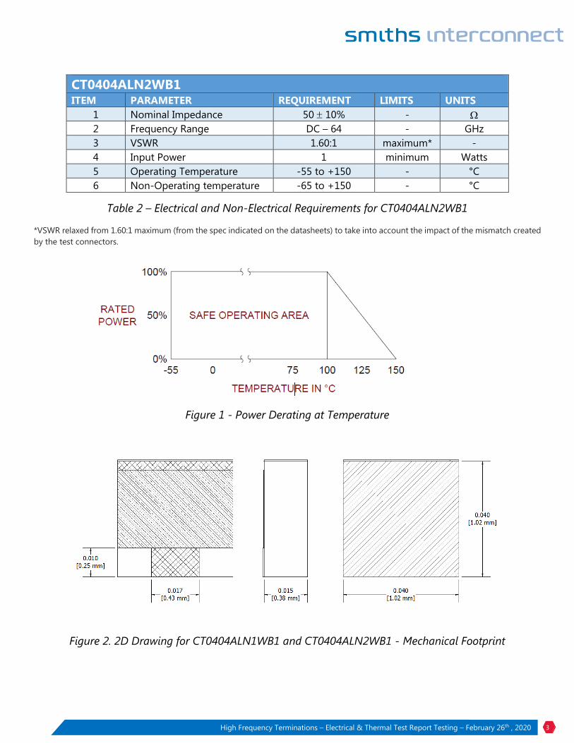
CT0404ALN2WB1 ITEM PARAMETER REQUIREMENT LIMITS UNITS
1 Nominal Impedance 50 10% -
2 Frequency Range DC – 64 - GHz
3 VSWR 1.60:1 maximum* -
4 Input Power 1 minimum Watts
5 Operating Temperature -55 to +150 - °C
6 Non-Operating temperature -65 to +150 - °C
Table 2 – Electrical and Non-Electrical Requirements for CT0404ALN2WB1
*VSWR relaxed from 1.60:1 maximum (from the spec indicated on the datasheets) to take into account the impact of the mismatch created
by the test connectors.
Figure 1 - Power Derating at Temperature
Figure 2. 2D Drawing for CT0404ALN1WB1 and CT0404ALN2WB1 - Mechanical Footprint
High Frequency Terminations – Electrical & Thermal Test Report Testing – February 26th , 2020 4
3. Test Preparation - Electrical (RF) Simulations
Both part numbers have been simulated in multiple 2.5D or 3D electromagnetic simulators including
Ansys HFSS, Dessault CST, National Instruments AWR, and Sonnet. The purpose of the modeling in
various simulation tools is to compare the simulated performance and to establish the level of
correlation between the simulation and the test.
After the designs have been optimized for a nominal performance, the tolerance analysis has been
conducted that considered substrate thickness and dielectric constant variations, transmission line
dimensional tolerances, and variations in the bulk resistivity and shape of the resistors.
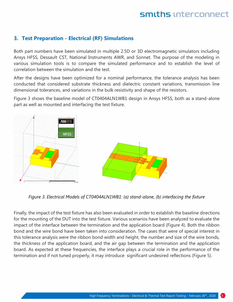
Figure 3 shows the baseline model of CT0404ALN1WB1 design in Ansys HFSS, both as a stand-alone
part as well as mounted and interfacing the test fixture.
Figure 3. Electrical Models of CT0404ALN1WB1: (a) stand-alone, (b) interfacing the fixture
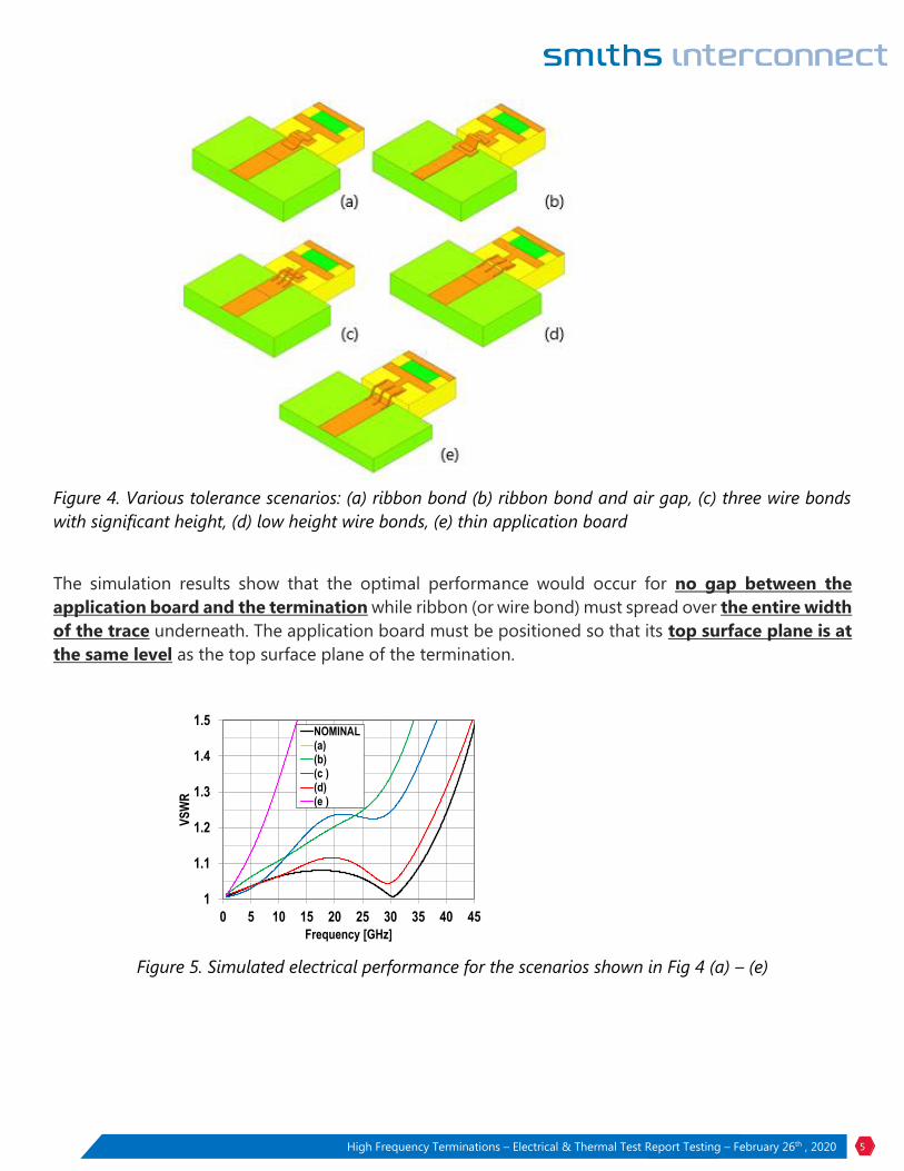
Finally, the impact of the test fixture has also been evaluated in order to establish the baseline directions
for the mounting of the DUT into the test fixture. Various scenarios have been analyzed to evaluate the
impact of the interface between the termination and the application board (Figure 4). Both the ribbon
bond and the wire bond have been taken into consideration. The cases that were of special interest in
this tolerance analysis were the ribbon bond width and height, the number and size of the wire bonds,
the thickness of the application board, and the air gap between the termination and the application
board. As expected at these frequencies, the interface plays a crucial role in the performance of the
termination and if not tuned properly, it may introduce significant undesired reflections (Figure 5).
High Frequency Terminations – Electrical & Thermal Test Report Testing – February 26th , 2020 5
Figure 4. Various tolerance scenarios: (a) ribbon bond (b) ribbon bond and air gap, (c) three wire bonds
with significant height, (d) low height wire bonds, (e) thin application board
The simulation results show that the optimal performance would occur for no gap between the
application board and the termination while ribbon (or wire bond) must spread over the entire width
of the trace underneath. The application board must be positioned so that its top surface plane is at
the same level as the top surface plane of the termination.
Figure 5. Simulated electrical performance for the scenarios shown in Fig 4 (a) – (e)
1
1.1
1.2
1.3
1.4
1.5
0 5 10 15 20 25 30 35 40 45
VS
WR
Frequency [GHz]
NOMINAL(a)(b)(c )(d)(e )
High Frequency Terminations – Electrical & Thermal Test Report Testing – February 26th , 2020 6
4. Test Fixture Choice
In order to properly fixture the presented RF termination and similar high frequency surface mount
components for RF performance verification testing, the information about the medium (substrate) onto
which the device will be mounted on during its intended field operation is needed. This is achieved by
spending effort in first constructing a ‘good’ 50 Ω transmission through line with the line width sized
to match the width of the DUT. The properties of PCB substrate such as dielectric constant and thickness
are chosen to yield a transmission line that closely matches the DUT I/O pad widths. To reduce radiation
losses, most of the test boards are realized in a grounded coplanar waveguide (CPWG) structure that
exhibits better performance than the traditional microstrip line test fixtures at frequencies above 20
GHz. In addition to the argument above, CPWG lines also work very well with SMT (surface-mount)
devices since the signal and ground are located on the same plane. The through line test fixture should
be sized to match the final DUT test fixture size.
Figure 6. Test board used to interface the DUT with the connector
Essentially, the through line length will be the size of the input launch times two. The DUT test fixture
length will be the through line length plus the DUT length for 2-port devices. A single port device, such
as a termination fixture length will be that one launch length (half of the through line) plus the DUT
length. The substrate thickness should be selected properly for the frequency of interest to avoid the
creation of higher order modes that appear as undesired spikes on the display of the vector network
analyzer (VNA). For the purpose of testing high frequency terminations CT0404ALN1WB1 and
CT0404ALN2WB1, a test board made on Rogers 4350 substrate is utilized (Figure 6).
The test fixture will also include some sort of coaxial connector and a transition from planar board into
the coaxial structure of the connector (Fig 4). The connector is chosen to support the operation
frequency band and desired VSWR. For the purpose of testing high frequency terminations
CT0404ALN1WB1 and CT0404ALN2WB1, we used Southwest Microwave field replaceable connectors:

High Frequency Terminations – Electrical & Thermal Test Report Testing – February 26th , 2020 7
2.4mm female (part #: 1492-03A-5) for CT0404ALN1WB1 (DC – 42.5 GHz)
1.85 mm female (part #: 1892-04A-6) for CT0404ALN2WB1 (DC – 64 GHz).
The 2.4 mm jack (female) end launch connector used for the tests at frequencies DC – 42.5 GHz is shown
in Figure 7. It is important to mention that the selection of the connector pin (see dimensions A) on
the connector (1.85mm or 2.4 mm) affects the connector launch performance and thus must be chosen
as directed.
Figure 7. Southwest Microwave 2.4 mm connector used in tests at frequencies DC-42.5 GHz (drawing)
5. Mounting Instructions
First step in properly mounting the RF termination for testing is to carefully inspect all the components
of the test fixture to be assembled. Special attention should be given to the test board edges (Figure
8a). Common PCB manufacturing often leave rough edges that can cause fixture assembly issues. The
edges of the test board can usually be cleaned up using fine grit sand paper. (Figure 8b).

High Frequency Terminations – Electrical & Thermal Test Report Testing – February 26th , 2020 8
Figure 8. Test board transmission line:
(a) rough edge (before cleaning), (b) smooth edge (after cleaning)
Next is the fixture assembly; the carrier board is soldered to the test board using Sn96 solder. Care
should be taken to insure there is no solder run-out into the area where the DUT is to be mounted. The
final step in the fixture assembly is to mount the connector to the test board. Things to look for at this
step is to center the connector pin on the transmission line and to insure the connector is flush with the
edge of the test board to avoid undesired air gaps (Figure 9). Use of a microscope is essential to insuring
that the connector is mounted properly.
Figure 9. Connector pin alignment on the test board
Having a properly assembled test fixture, it is time to mount the RF termination. The RF termination
should also be inspected to insure the edges are cleanly cut and have no jagged edges prior to being
installed on the test fixture. Due to possible power handling requirements, the RF termination needs to
be soldered in place. This presents challenges in proper alignment to the transmission line. When
soldering, the termination tends to move during solder reflow. To prevent this, pure indium solder could
be used. The indium solder is very soft, and the termination can be pressed into the solder before reflow
(a) (b)
High Frequency Terminations – Electrical & Thermal Test Report Testing – February 26th , 2020 9
which allows for fine adjustment of the termination to the transmission line and to ensure the
termination is flush with the test board. When the termination is reflowed, it remains in place. Finally,
the termination needs to be connected to the transmission line. There are primarily two types of
connection methods, ribbon and wire bonding. Short ribbon bonds provide the best RF performance,
but wire bonding is the most popular. In order to analyze the effects of the different connection
methods, it is important to use the same termination. This can prove difficult as removing the ribbon
or wire bonds can often damage the circuit. In order to prevent any damage, the ribbon bond can be
replaced with a small piece of indium solder. The indium solder does not need to be reflowed but just
pressed into place. The pliability of the indium allows for good contact to the transmission line and the
termination. It can then be easily removed and replaced with the wire bonds. This allows for a direct
comparison of the effects of the different connection methods using the identical termination and
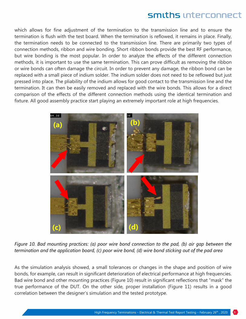
fixture. All good assembly practice start playing an extremely important role at high frequencies.
Figure 10. Bad mounting practices: (a) poor wire bond connection to the pad, (b) air gap between the
termination and the application board, (c) poor wire bond, (d) wire bond sticking out of the pad area
As the simulation analysis showed, a small tolerances or changes in the shape and position of wire
bonds, for example, can result in significant deterioration of electrical performance at high frequencies.
Bad wire bond and other mounting practices (Figure 10) result in significant reflections that “mask” the
true performance of the DUT. On the other side, proper installation (Figure 11) results in a good
correlation between the designer’s simulation and the tested prototype.
(a) (b)
(c) (d)
High Frequency Terminations – Electrical & Thermal Test Report Testing – February 26th , 2020 10
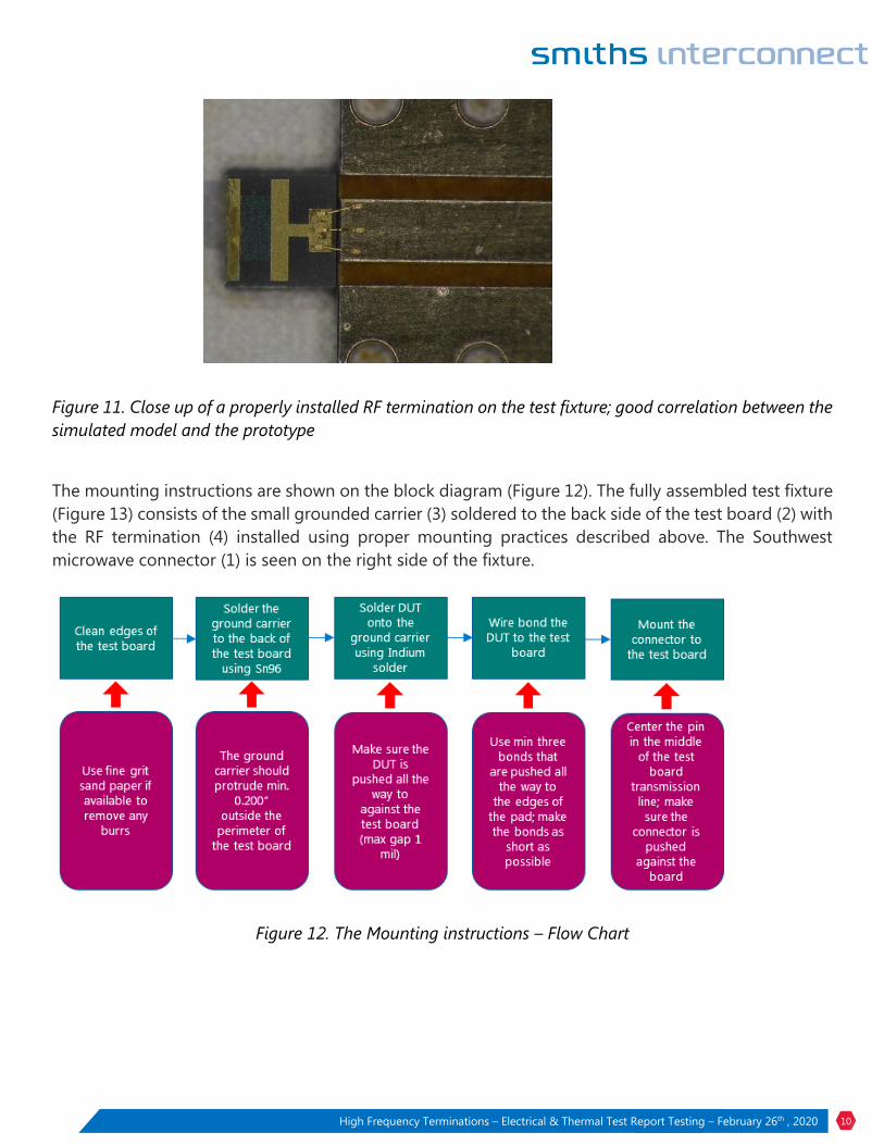
Figure 11. Close up of a properly installed RF termination on the test fixture; good correlation between the
simulated model and the prototype
The mounting instructions are shown on the block diagram (Figure 12). The fully assembled test fixture
(Figure 13) consists of the small grounded carrier (3) soldered to the back side of the test board (2) with
the RF termination (4) installed using proper mounting practices described above. The Southwest
microwave connector (1) is seen on the right side of the fixture.
Figure 12. The Mounting instructions – Flow Chart

High Frequency Terminations – Electrical & Thermal Test Report Testing – February 26th , 2020 11
Figure 13. Fully assembled test fixture used in the electrical test of high frequency terminations: 1 –
connector, 2 – test board, 3 – ground carrier, 4 – DUT (RF termination)
High Frequency Terminations – Electrical & Thermal Test Report Testing – February 26th , 2020 12
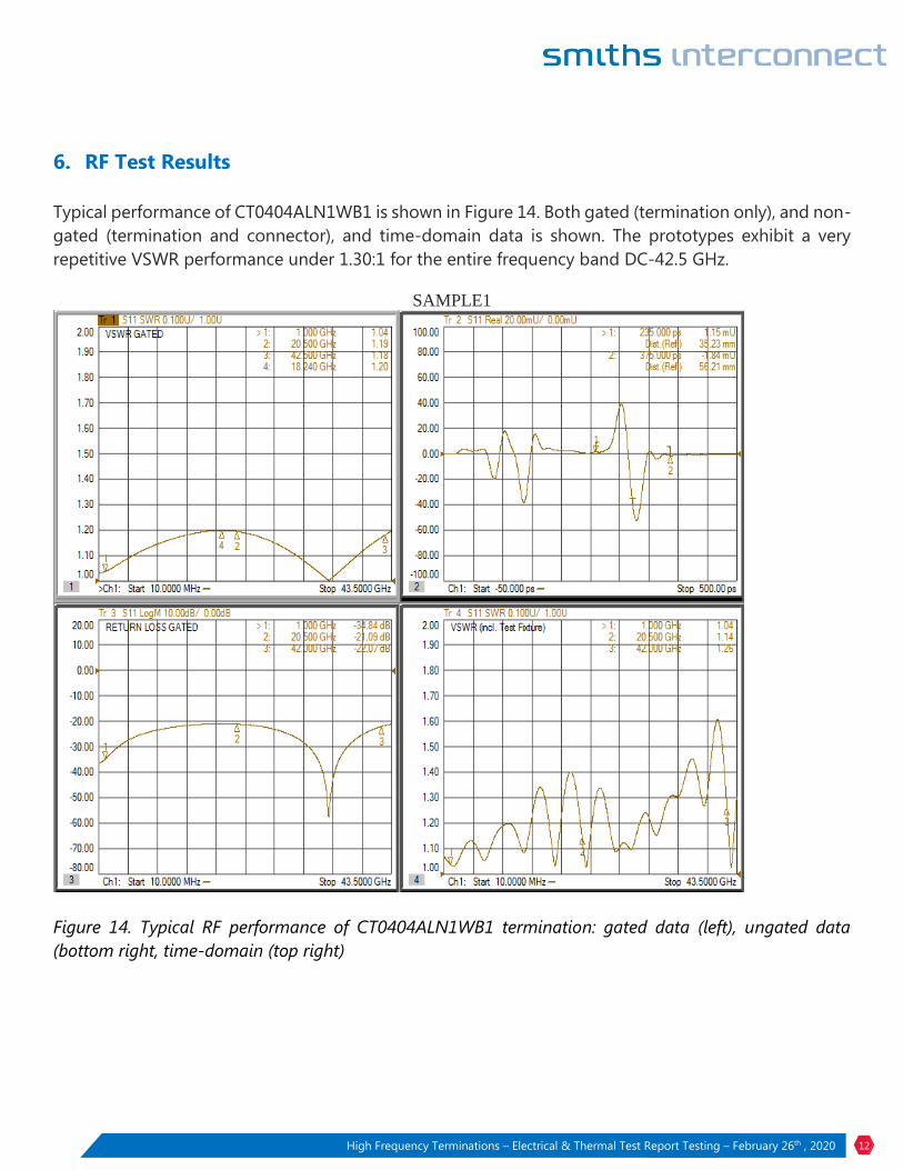
6. RF Test Results
Typical performance of CT0404ALN1WB1 is shown in Figure 14. Both gated (termination only), and non-
gated (termination and connector), and time-domain data is shown. The prototypes exhibit a very
repetitive VSWR performance under 1.30:1 for the entire frequency band DC-42.5 GHz.
SAMPLE1
Figure 14. Typical RF performance of CT0404ALN1WB1 termination: gated data (left), ungated data
(bottom right, time-domain (top right)

High Frequency Terminations – Electrical & Thermal Test Report Testing – February 26th , 2020 13
Typical performance of CT0404ALN2WB1 is shown in Figure 15. Both gated (termination only), non-
gated (termination and connector) data, and time domain data is shown. The prototypes exhibit a very
repetitive VSWR performance under 1.30:1 for the entire frequency band DC-64 GHz.
SAMPLE 1
Figure 15. Typical RF performance of CT0404ALN2WB1 termination: ungated data (top left), gated data
(right), time domain data (bottom left)
7. Thermal (FEA) Simulation
Thermal FEA simulation has been performed on both RF terminations. Two types of thermal analysis
are conducted - with input power at DC using SolidWorks and with input power at RF frequencies using
CST MPHYSICS® STUDIO.
CST MPHYSICS® STUDIO (CST MPS) is a powerful and easy-to-use tool for thermal and mechanical
stress analysis. High-frequency fields, currents and particle collisions are all sources of heat that EM
engineers frequently encounter, and so CST MPS is fully integrated into CST STUDIO SUITE® to enable
coupled EM-multiphysics simulation with other tools such as CST MICROWAVE STUDIO®, CST EM
High Frequency Terminations – Electrical & Thermal Test Report Testing – February 26th , 2020 14
STUDIO® and CST PARTICLE STUDIO®. With the CST MPS thermal solver, the changes in temperature
generated by these interactions are modeled, and heat flow within the device simulated to test the
performance of heat sinks and ensure the reliability of temperature-sensitive components. From the
temperature distribution, CST MPS® can also calculate the thermal expansion of the components and
the stress and strain within it as it presses against its housing, using the mechanical solver. The results
of the thermal expansion simulation can even be fed back into the EM simulations, offering the
opportunity to perform a sensitivity analysis of the device’s response to heating.
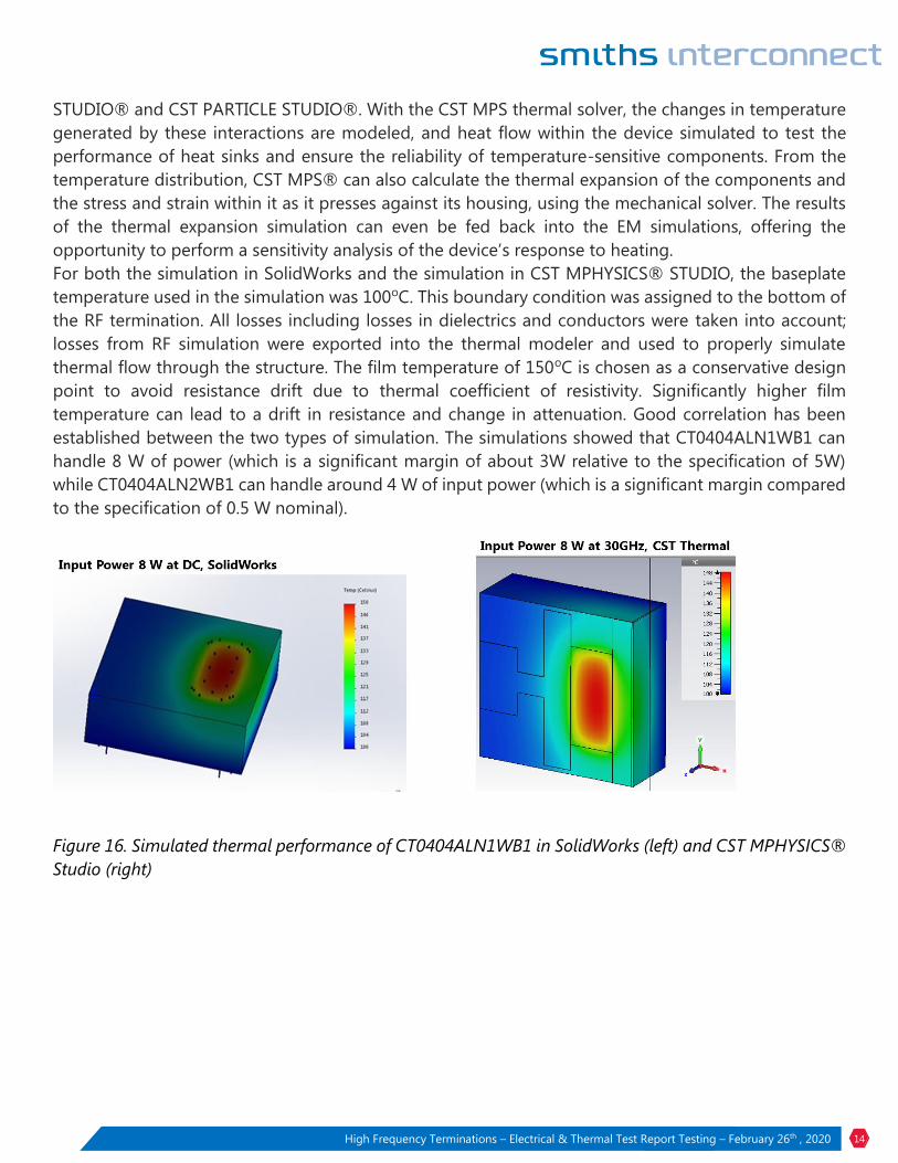
For both the simulation in SolidWorks and the simulation in CST MPHYSICS® STUDIO, the baseplate
temperature used in the simulation was 100oC. This boundary condition was assigned to the bottom of
the RF termination. All losses including losses in dielectrics and conductors were taken into account;
losses from RF simulation were exported into the thermal modeler and used to properly simulate
thermal flow through the structure. The film temperature of 150oC is chosen as a conservative design
point to avoid resistance drift due to thermal coefficient of resistivity. Significantly higher film
temperature can lead to a drift in resistance and change in attenuation. Good correlation has been
established between the two types of simulation. The simulations showed that CT0404ALN1WB1 can
handle 8 W of power (which is a significant margin of about 3W relative to the specification of 5W)
while CT0404ALN2WB1 can handle around 4 W of input power (which is a significant margin compared
to the specification of 0.5 W nominal).
Figure 16. Simulated thermal performance of CT0404ALN1WB1 in SolidWorks (left) and CST MPHYSICS®
Studio (right)
High Frequency Terminations – Electrical & Thermal Test Report Testing – February 26th , 2020 15
Figure 17. Simulated thermal performance of CT0404ALN2WB1 in SolidWorks (left) and CST MPHYSICS®
Studio (right)
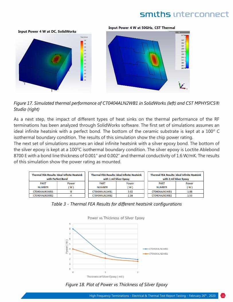
As a next step, the impact of different types of heat sinks on the thermal performance of the RF
terminations has been analyzed through SolidWorks software. The first set of simulations assumes an
ideal infinite heatsink with a perfect bond. The bottom of the ceramic substrate is kept at a 100o C
isothermal boundary condition. The results of this simulation show the chip power rating.
The next set of simulations assumes an ideal infinite heatsink with a silver epoxy bond. The bottom of
the silver epoxy is kept at a 100oC isothermal boundary condition. The silver epoxy is Loctite Ablebond
8700 E with a bond line thickness of 0.001” and 0.002” and thermal conductivity of 1.6 W/mK. The results
of this simulation show the power rating as mounted.
Table 3 - Thermal FEA Results for different heatsink configurations
Figure 18. Plot of Power vs Thickness of Silver Epoxy
High Frequency Terminations – Electrical & Thermal Test Report Testing – February 26th , 2020 16
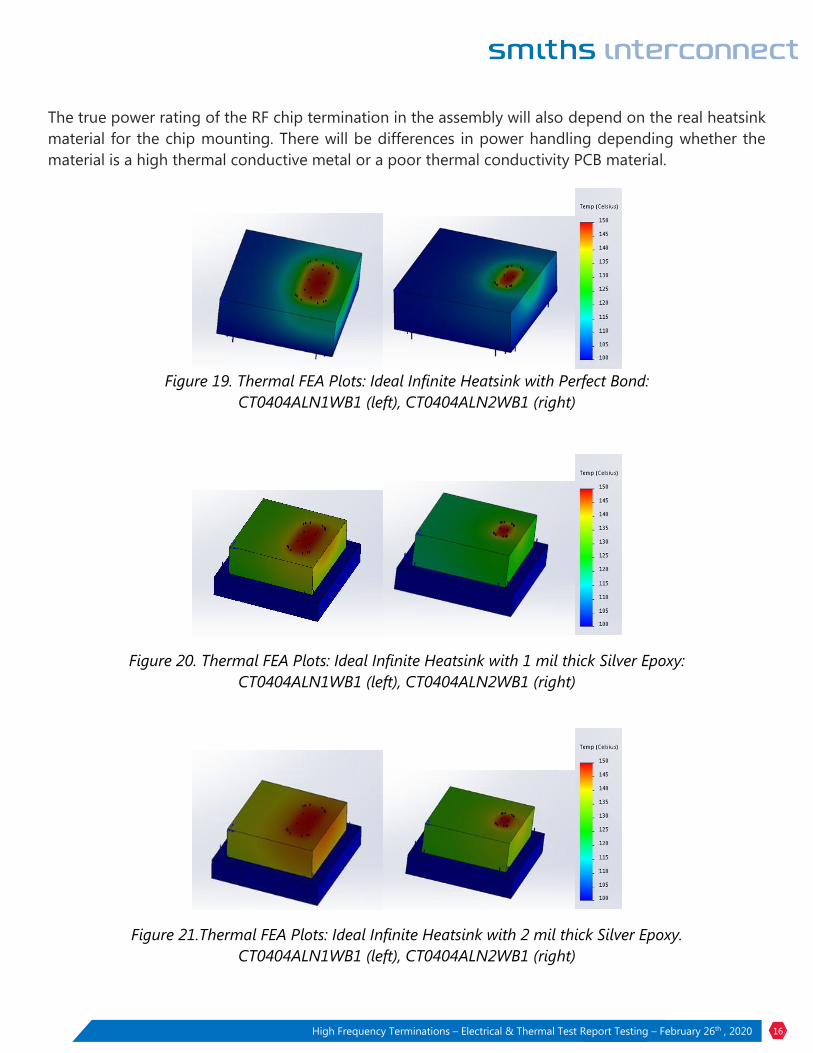
The true power rating of the RF chip termination in the assembly will also depend on the real heatsink
material for the chip mounting. There will be differences in power handling depending whether the
material is a high thermal conductive metal or a poor thermal conductivity PCB material.
Figure 19. Thermal FEA Plots: Ideal Infinite Heatsink with Perfect Bond:
CT0404ALN1WB1 (left), CT0404ALN2WB1 (right)
Figure 20. Thermal FEA Plots: Ideal Infinite Heatsink with 1 mil thick Silver Epoxy:
CT0404ALN1WB1 (left), CT0404ALN2WB1 (right)
Figure 21.Thermal FEA Plots: Ideal Infinite Heatsink with 2 mil thick Silver Epoxy.
CT0404ALN1WB1 (left), CT0404ALN2WB1 (right)
High Frequency Terminations – Electrical & Thermal Test Report Testing – February 26th , 2020 17
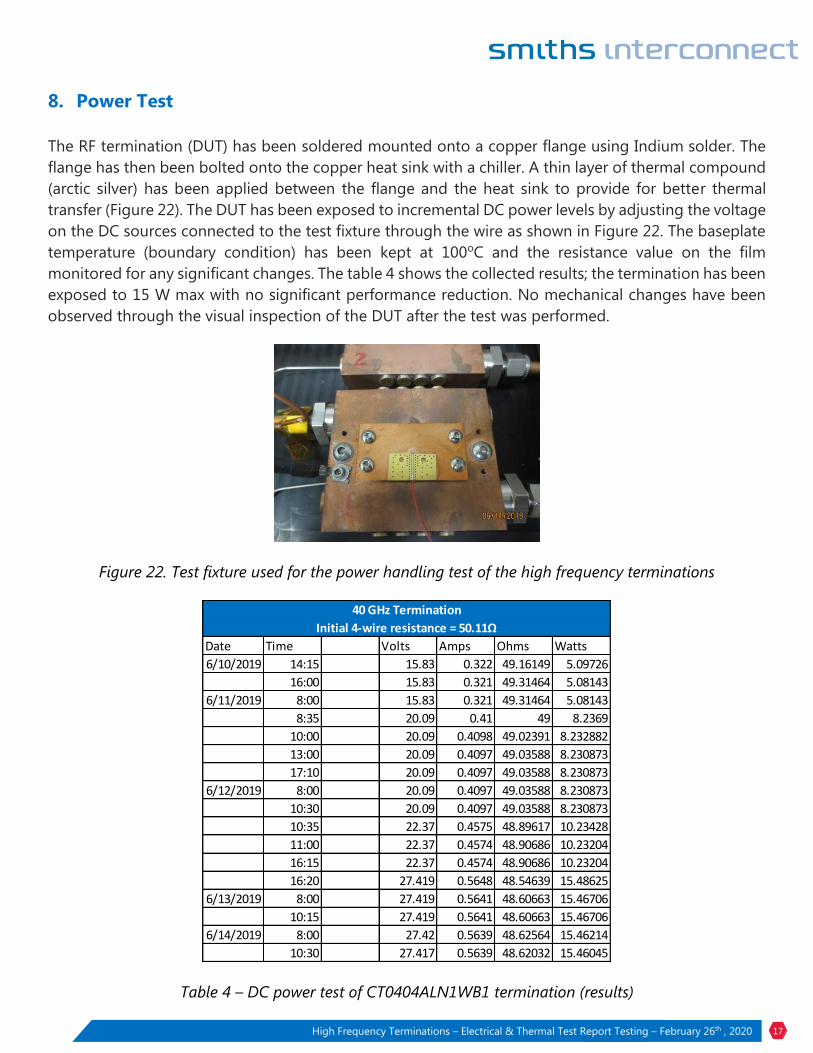
8. Power Test
The RF termination (DUT) has been soldered mounted onto a copper flange using Indium solder. The
flange has then been bolted onto the copper heat sink with a chiller. A thin layer of thermal compound
(arctic silver) has been applied between the flange and the heat sink to provide for better thermal
transfer (Figure 22). The DUT has been exposed to incremental DC power levels by adjusting the voltage
on the DC sources connected to the test fixture through the wire as shown in Figure 22. The baseplate
temperature (boundary condition) has been kept at 100oC and the resistance value on the film
monitored for any significant changes. The table 4 shows the collected results; the termination has been
exposed to 15 W max with no significant performance reduction. No mechanical changes have been
observed through the visual inspection of the DUT after the test was performed.
Figure 22. Test fixture used for the power handling test of the high frequency terminations
Table 4 – DC power test of CT0404ALN1WB1 termination (results)
Date Time Volts Amps Ohms Watts
6/10/2019 14:15 15.83 0.322 49.16149 5.09726
16:00 15.83 0.321 49.31464 5.08143
6/11/2019 8:00 15.83 0.321 49.31464 5.08143
8:35 20.09 0.41 49 8.2369
10:00 20.09 0.4098 49.02391 8.232882
13:00 20.09 0.4097 49.03588 8.230873
17:10 20.09 0.4097 49.03588 8.230873
6/12/2019 8:00 20.09 0.4097 49.03588 8.230873
10:30 20.09 0.4097 49.03588 8.230873
10:35 22.37 0.4575 48.89617 10.23428
11:00 22.37 0.4574 48.90686 10.23204
16:15 22.37 0.4574 48.90686 10.23204
16:20 27.419 0.5648 48.54639 15.48625
6/13/2019 8:00 27.419 0.5641 48.60663 15.46706
10:15 27.419 0.5641 48.60663 15.46706
6/14/2019 8:00 27.42 0.5639 48.62564 15.46214
10:30 27.417 0.5639 48.62032 15.46045
40 GHz Termination
Initial 4-wire resistance = 50.11Ω
High Frequency Terminations – Electrical & Thermal Test Report Testing – February 26th , 2020 18
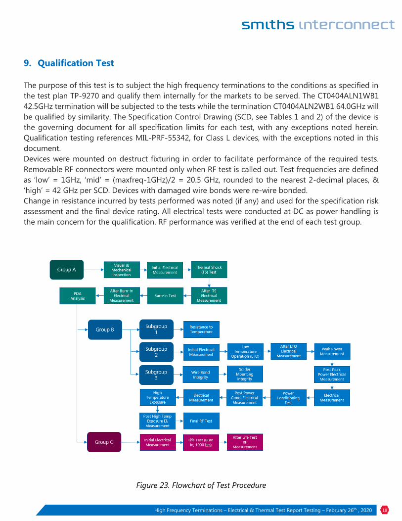
9. Qualification Test
The purpose of this test is to subject the high frequency terminations to the conditions as specified in
the test plan TP-9270 and qualify them internally for the markets to be served. The CT0404ALN1WB1
42.5GHz termination will be subjected to the tests while the termination CT0404ALN2WB1 64.0GHz will
be qualified by similarity. The Specification Control Drawing (SCD, see Tables 1 and 2) of the device is
the governing document for all specification limits for each test, with any exceptions noted herein.
Qualification testing references MIL-PRF-55342, for Class L devices, with the exceptions noted in this
document.
Devices were mounted on destruct fixturing in order to facilitate performance of the required tests.
Removable RF connectors were mounted only when RF test is called out. Test frequencies are defined
as ‘low’ = 1GHz, ‘mid’ = (maxfreq-1GHz)/2 = 20.5 GHz, rounded to the nearest 2-decimal places, &
‘high’ = 42 GHz per SCD. Devices with damaged wire bonds were re-wire bonded.
Change in resistance incurred by tests performed was noted (if any) and used for the specification risk
assessment and the final device rating. All electrical tests were conducted at DC as power handling is
the main concern for the qualification. RF performance was verified at the end of each test group.
Figure 23. Flowchart of Test Procedure
High Frequency Terminations – Electrical & Thermal Test Report Testing – February 26th , 2020 19
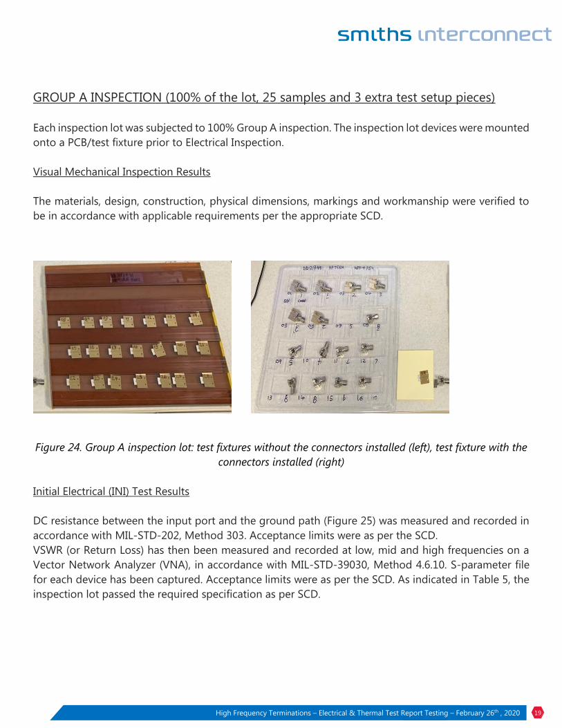
GROUP A INSPECTION (100% of the lot, 25 samples and 3 extra test setup pieces)
Each inspection lot was subjected to 100% Group A inspection. The inspection lot devices were mounted
onto a PCB/test fixture prior to Electrical Inspection.
Visual Mechanical Inspection Results
The materials, design, construction, physical dimensions, markings and workmanship were verified to
be in accordance with applicable requirements per the appropriate SCD.
Figure 24. Group A inspection lot: test fixtures without the connectors installed (left), test fixture with the
connectors installed (right)
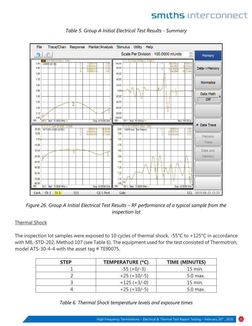
Initial Electrical (INI) Test Results
DC resistance between the input port and the ground path (Figure 25) was measured and recorded in
accordance with MIL-STD-202, Method 303. Acceptance limits were as per the SCD.
VSWR (or Return Loss) has then been measured and recorded at low, mid and high frequencies on a
Vector Network Analyzer (VNA), in accordance with MIL-STD-39030, Method 4.6.10. S-parameter file
for each device has been captured. Acceptance limits were as per the SCD. As indicated in Table 5, the
inspection lot passed the required specification as per SCD.

High Frequency Terminations – Electrical & Thermal Test Report Testing – February 26th , 2020 20
Figure 25. DC resistance test schematic diagram
HF Series Terminations per Test Plan TP-9270
Test Group A Part Number
Test Sequence A2 Description
Test StepInitial Electrical (DC & RF)
InspectionRevision
Quantity 28 Test Plan
Date In 8/28/2019 Factory Order
Date Out 8/30/2019 Lot Code
Operator JA Results
Nominal Resistance Value 50 Ω
Upper Limit DCR 55 Ω
Lower Limit DCR 45 Ω
VSWR Limit 1.36 :1
Serial Number DC Resistance (Ω) VSWR @ 1 GHz VSWR @ 20.5 GHz VSWR @ 42 GHz
1 47.23 1.04 1.30 1.18
2 50.26 1.04 1.30 1.23
3 47.08 1.04 1.32 1.19
4 47.02 1.04 1.33 1.15
5 50.03 1.05 1.30 1.14
6 47.70 1.03 1.33 1.18
7 47.73 1.03 1.31 1.16
8 47.60 1.03 1.31 1.15
9 47.39 1.04 1.30 1.16
10 47.23 1.04 1.33 1.17
11 51.20 1.06 1.24 1.14
12 50.62 1.04 1.25 1.17
13 50.57 1.06 1.26 1.19
14 47.57 1.03 1.30 1.16
15 47.57 1.03 1.29 1.15
16 48.57 1.02 1.30 1.16
17 48.09 1.03 1.29 1.16
18 48.19 1.03 1.32 1.20
19 48.29 1.03 1.36 1.18
20 48.44 1.03 1.31 1.18
21 48.09 1.03 1.32 1.22
22 48.35 1.02 1.32 1.19
23 47.49 1.03 1.35 1.22
24 48.21 1.03 1.31 1.18
25 48.62 1.02 1.35 1.17
26 51.37 1.06 1.26 1.20
27 47.15 1.03 1.31 1.16
28 52.71 1.10 1.22 1.23
Initial Measurements
REF 4759
REF 4759
CT0404ALN1WB1
42GHz HF Termination, Wire bondable
-
TP-9270
Pass
High Frequency Terminations – Electrical & Thermal Test Report Testing – February 26th , 2020 21
Table 5. Group A Initial Electrical Test Results - Summary
Figure 26. Group A Initial Electrical Test Results – RF performance of a typical sample from the
inspection lot
Thermal Shock
The inspection lot samples were exposed to 10 cycles of thermal shock, -55°C to +125°C in accordance
with MIL-STD-202, Method 107 (see Table 6). The equipment used for the test consisted of Thermotron,
model ATS-30-4-4 with the asset tag # TE90075.
STEP TEMPERATURE (ºC) TIME (MINUTES)
1 -55 (+0/-3) 15 min.
2 +25 (+10/-5) 5.0 max.
3 +125 (+3/-0) 15 min.
4 +25 (+10/-5) 5.0 max.
Table 6. Thermal Shock temperature levels and exposure times
High Frequency Terminations – Electrical & Thermal Test Report Testing – February 26th , 2020 22
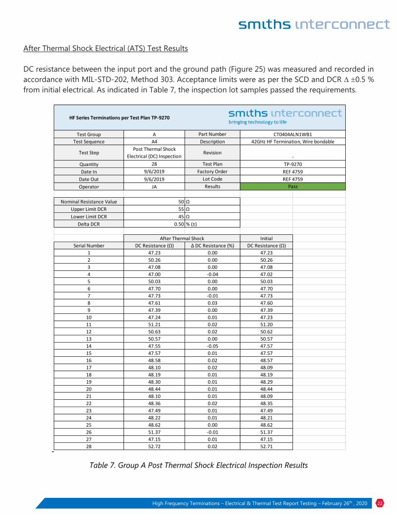
After Thermal Shock Electrical (ATS) Test Results
DC resistance between the input port and the ground path (Figure 25) was measured and recorded in
accordance with MIL-STD-202, Method 303. Acceptance limits were as per the SCD and DCR 0.5 %
from initial electrical. As indicated in Table 7, the inspection lot samples passed the requirements.
Table 7. Group A Post Thermal Shock Electrical Inspection Results
HF Series Terminations per Test Plan TP-9270
Test Group A Part Number
Test Sequence A4 Description
Test StepPost Thermal Shock
Electrical (DC) InspectionRevision
Quantity 28 Test Plan
Date In 9/6/2019 Factory Order
Date Out 9/6/2019 Lot Code
Operator JA Results
Nominal Resistance Value 50 Ω
Upper Limit DCR 55 Ω
Lower Limit DCR 45 Ω
Delta DCR 0.50 % (±)
Initial
Serial Number DC Resistance (Ω) Δ DC Resistance (%) DC Resistance (Ω)
1 47.23 0.00 47.23
2 50.26 0.00 50.26
3 47.08 0.00 47.08
4 47.00 -0.04 47.02
5 50.03 0.00 50.03
6 47.70 0.00 47.70
7 47.73 -0.01 47.73
8 47.61 0.03 47.60
9 47.39 0.00 47.39
10 47.24 0.01 47.23
11 51.21 0.02 51.20
12 50.63 0.02 50.62
13 50.57 0.00 50.57
14 47.55 -0.05 47.57
15 47.57 0.01 47.57
16 48.58 0.02 48.57
17 48.10 0.02 48.09
18 48.19 0.01 48.19
19 48.30 0.01 48.29
20 48.44 0.01 48.44
21 48.10 0.01 48.09
22 48.36 0.02 48.35
23 47.49 0.01 47.49
24 48.22 0.01 48.21
25 48.62 0.00 48.62
26 51.37 -0.01 51.37
27 47.15 0.01 47.15
28 52.72 0.02 52.71
Pass
After Thermal Shock
REF 4759
REF 4759
CT0404ALN1WB1
42GHz HF Termination, Wire bondable
-
TP-9270
High Frequency Terminations – Electrical & Thermal Test Report Testing – February 26th , 2020 23
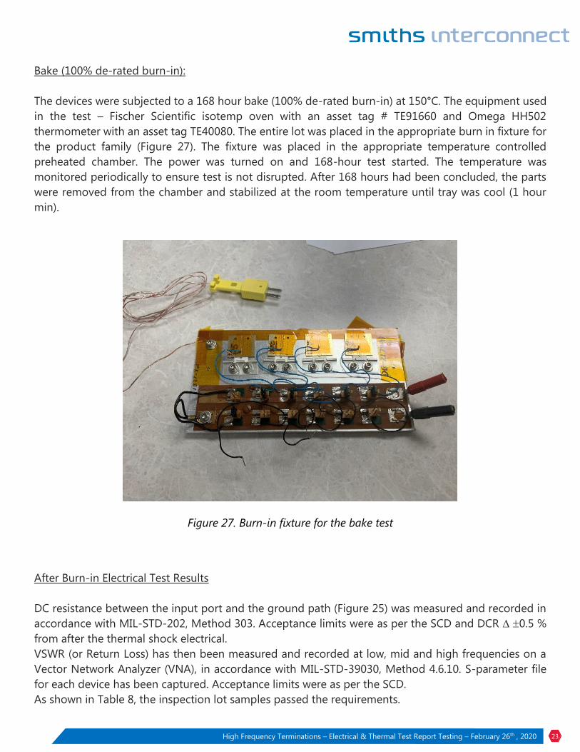
Bake (100% de-rated burn-in):
The devices were subjected to a 168 hour bake (100% de-rated burn-in) at 150°C. The equipment used
in the test – Fischer Scientific isotemp oven with an asset tag # TE91660 and Omega HH502
thermometer with an asset tag TE40080. The entire lot was placed in the appropriate burn in fixture for
the product family (Figure 27). The fixture was placed in the appropriate temperature controlled
preheated chamber. The power was turned on and 168-hour test started. The temperature was
monitored periodically to ensure test is not disrupted. After 168 hours had been concluded, the parts
were removed from the chamber and stabilized at the room temperature until tray was cool (1 hour
min).
Figure 27. Burn-in fixture for the bake test
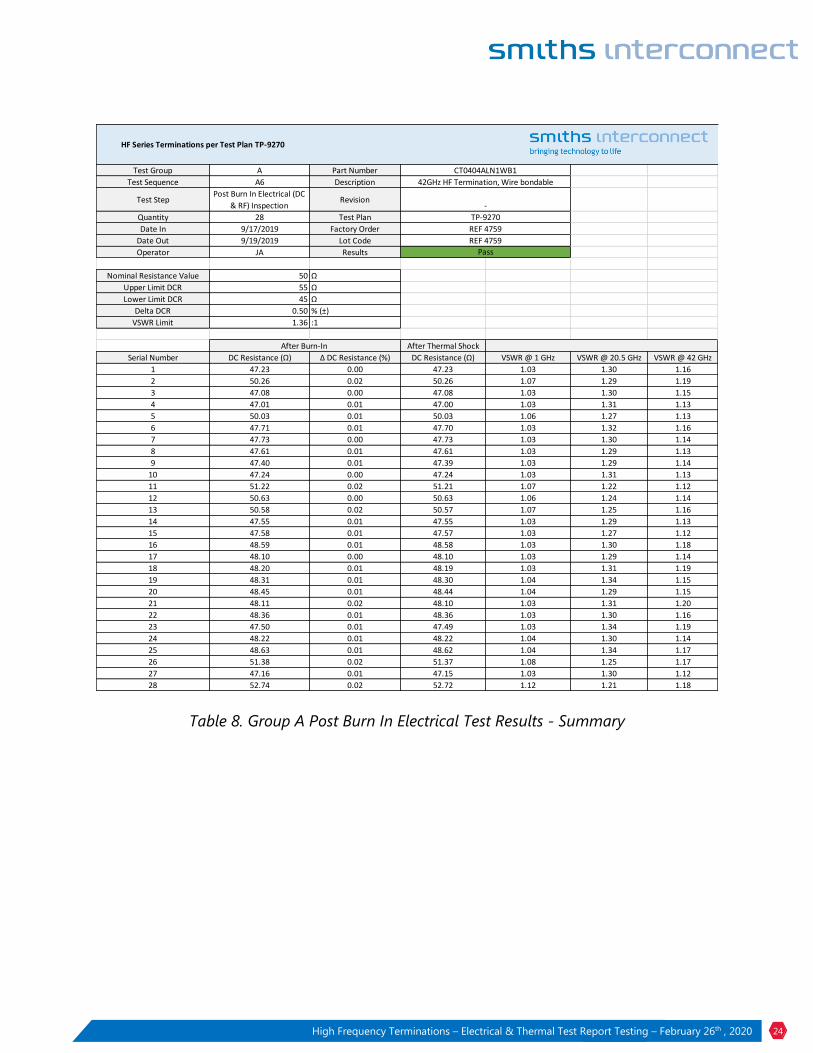
After Burn-in Electrical Test Results
DC resistance between the input port and the ground path (Figure 25) was measured and recorded in
accordance with MIL-STD-202, Method 303. Acceptance limits were as per the SCD and DCR 0.5 %
from after the thermal shock electrical.
VSWR (or Return Loss) has then been measured and recorded at low, mid and high frequencies on a
Vector Network Analyzer (VNA), in accordance with MIL-STD-39030, Method 4.6.10. S-parameter file
for each device has been captured. Acceptance limits were as per the SCD.
As shown in Table 8, the inspection lot samples passed the requirements.
High Frequency Terminations – Electrical & Thermal Test Report Testing – February 26th , 2020 24
Table 8. Group A Post Burn In Electrical Test Results - Summary
HF Series Terminations per Test Plan TP-9270
Test Group A Part Number
Test Sequence A6 Description
Test StepPost Burn In Electrical (DC
& RF) InspectionRevision
Quantity 28 Test Plan
Date In 9/17/2019 Factory Order
Date Out 9/19/2019 Lot Code
Operator JA Results
Nominal Resistance Value 50 Ω
Upper Limit DCR 55 Ω
Lower Limit DCR 45 Ω
Delta DCR 0.50 % (±)
VSWR Limit 1.36 :1
After Thermal Shock
Serial Number DC Resistance (Ω) Δ DC Resistance (%) DC Resistance (Ω) VSWR @ 1 GHz VSWR @ 20.5 GHz VSWR @ 42 GHz
1 47.23 0.00 47.23 1.03 1.30 1.16
2 50.26 0.02 50.26 1.07 1.29 1.19
3 47.08 0.00 47.08 1.03 1.30 1.15
4 47.01 0.01 47.00 1.03 1.31 1.13
5 50.03 0.01 50.03 1.06 1.27 1.13
6 47.71 0.01 47.70 1.03 1.32 1.16
7 47.73 0.00 47.73 1.03 1.30 1.14
8 47.61 0.01 47.61 1.03 1.29 1.13
9 47.40 0.01 47.39 1.03 1.29 1.14
10 47.24 0.00 47.24 1.03 1.31 1.13
11 51.22 0.02 51.21 1.07 1.22 1.12
12 50.63 0.00 50.63 1.06 1.24 1.14
13 50.58 0.02 50.57 1.07 1.25 1.16
14 47.55 0.01 47.55 1.03 1.29 1.13
15 47.58 0.01 47.57 1.03 1.27 1.12
16 48.59 0.01 48.58 1.03 1.30 1.18
17 48.10 0.00 48.10 1.03 1.29 1.14
18 48.20 0.01 48.19 1.03 1.31 1.19
19 48.31 0.01 48.30 1.04 1.34 1.15
20 48.45 0.01 48.44 1.04 1.29 1.15
21 48.11 0.02 48.10 1.03 1.31 1.20
22 48.36 0.01 48.36 1.03 1.30 1.16
23 47.50 0.01 47.49 1.03 1.34 1.19
24 48.22 0.01 48.22 1.04 1.30 1.14
25 48.63 0.01 48.62 1.04 1.34 1.17
26 51.38 0.02 51.37 1.08 1.25 1.17
27 47.16 0.01 47.15 1.03 1.30 1.12
28 52.74 0.02 52.72 1.12 1.21 1.18
Pass
After Burn-In
CT0404ALN1WB1
42GHz HF Termination, Wire bondable
-
TP-9270
REF 4759
REF 4759
High Frequency Terminations – Electrical & Thermal Test Report Testing – February 26th , 2020 25
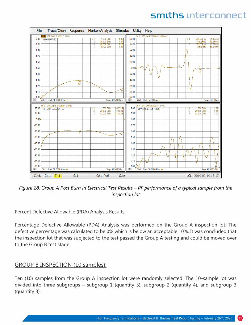
Figure 28. Group A Post Burn In Electrical Test Results – RF performance of a typical sample from the
inspection lot
Percent Defective Allowable (PDA) Analysis Results
Percentage Defective Allowable (PDA) Analysis was performed on the Group A inspection lot. The
defective percentage was calculated to be 0% which is below an acceptable 10%. It was concluded that
the inspection lot that was subjected to the test passed the Group A testing and could be moved over
to the Group B test stage.
GROUP B INSPECTION (10 samples):
Ten (10) samples from the Group A inspection lot were randomly selected. The 10-sample lot was
divided into three subgroups – subgroup 1 (quantity 3), subgroup 2 (quantity 4), and subgroup 3
(quantity 3).
High Frequency Terminations – Electrical & Thermal Test Report Testing – February 26th , 2020 26
SUBGROUP 1 (3pc sample) TEST RESULTS
Resistance to Temperature Characteristics
Devices were tested in accordance with MIL-STD-202, Method 304. The test was performed according
to the following details and exceptions:
Reference temperature: room ambient temperature.
Test temperatures:
o Step 1: room temperature.
o Step 2: -55°C.
o Step 3: room temperature.
o Step 4: +125°C.
Accuracy of temperature measurement: Devices were maintained within 3˚C of each test
temperature for a period of 30 to 45 minutes. Acceptance limits: per the SCD.
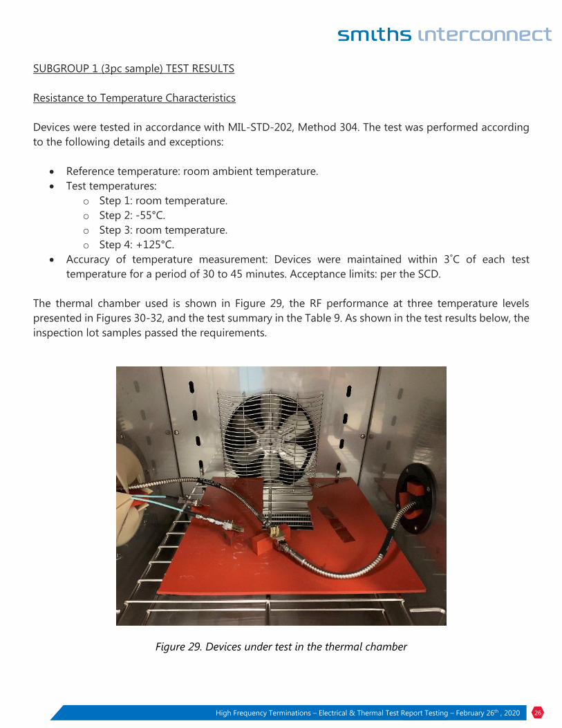
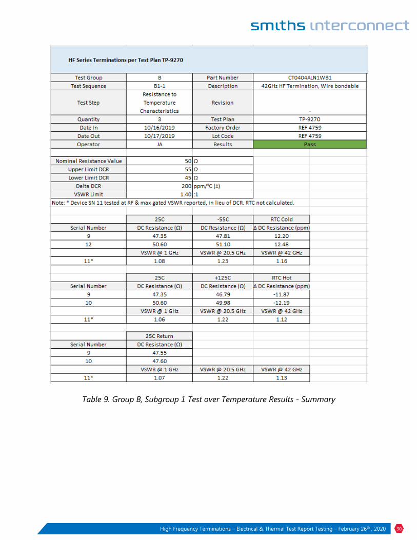
The thermal chamber used is shown in Figure 29, the RF performance at three temperature levels
presented in Figures 30-32, and the test summary in the Table 9. As shown in the test results below, the
inspection lot samples passed the requirements.
Figure 29. Devices under test in the thermal chamber
High Frequency Terminations – Electrical & Thermal Test Report Testing – February 26th , 2020 27
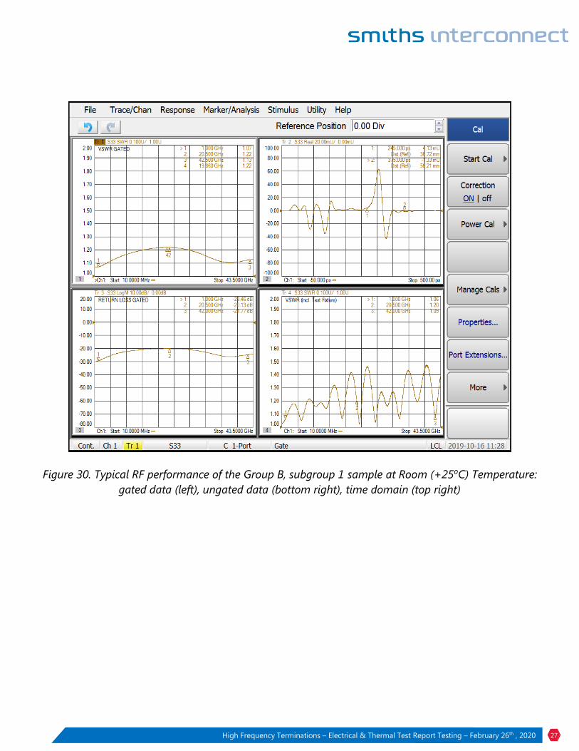
Figure 30. Typical RF performance of the Group B, subgroup 1 sample at Room (+25oC) Temperature:
gated data (left), ungated data (bottom right), time domain (top right)
High Frequency Terminations – Electrical & Thermal Test Report Testing – February 26th , 2020 28
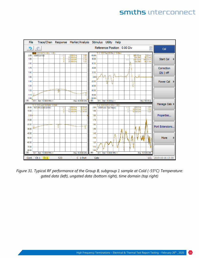
Figure 31. Typical RF performance of the Group B, subgroup 1 sample at Cold (-55oC) Temperature:
gated data (left), ungated data (bottom right), time domain (top right)
High Frequency Terminations – Electrical & Thermal Test Report Testing – February 26th , 2020 29
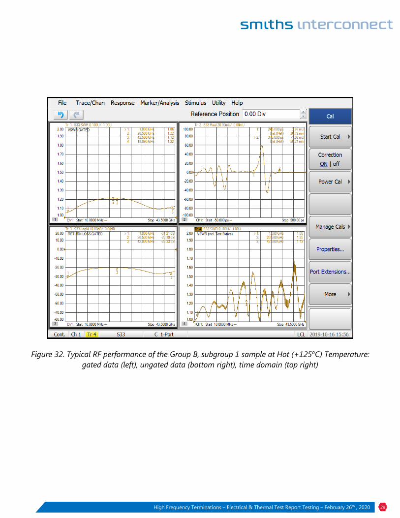
Figure 32. Typical RF performance of the Group B, subgroup 1 sample at Hot (+125oC) Temperature:
gated data (left), ungated data (bottom right), time domain (top right)
High Frequency Terminations – Electrical & Thermal Test Report Testing – February 26th , 2020 30
Table 9. Group B, Subgroup 1 Test over Temperature Results - Summary
High Frequency Terminations – Electrical & Thermal Test Report Testing – February 26th , 2020 31
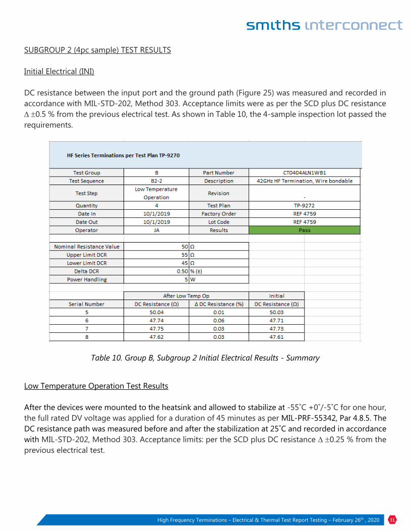
SUBGROUP 2 (4pc sample) TEST RESULTS
Initial Electrical (INI)
DC resistance between the input port and the ground path (Figure 25) was measured and recorded in
accordance with MIL-STD-202, Method 303. Acceptance limits were as per the SCD plus DC resistance
0.5 % from the previous electrical test. As shown in Table 10, the 4-sample inspection lot passed the
requirements.
Table 10. Group B, Subgroup 2 Initial Electrical Results - Summary
Low Temperature Operation Test Results
After the devices were mounted to the heatsink and allowed to stabilize at -55˚C +0˚/-5˚C for one hour,
the full rated DV voltage was applied for a duration of 45 minutes as per MIL-PRF-55342, Par 4.8.5. The
DC resistance path was measured before and after the stabilization at 25˚C and recorded in accordance
with MIL-STD-202, Method 303. Acceptance limits: per the SCD plus DC resistance 0.25 % from the
previous electrical test.

High Frequency Terminations – Electrical & Thermal Test Report Testing – February 26th , 2020 32
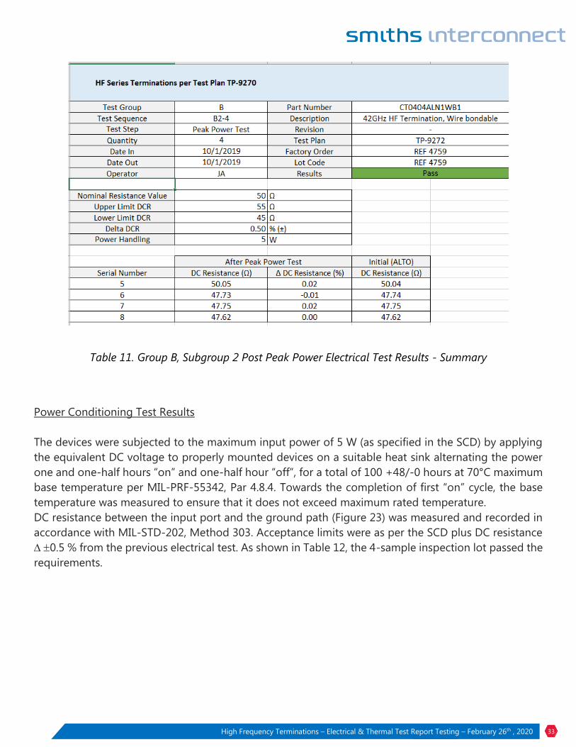
Peak Power Test Results
The devices were mounted on a suitable heatsink and subjected to peak power with the following
characteristics DC pulse characteristics: 10 ms pulse duration and 1% duty cycle (1millisecond period)
at ten times (10X) the maximum continuous power of 5 W, as per MIL-DTL-3933, Par 4.7.11.7. Devices
were mounted on a suitable heatsink (see Figure 33).
Figure 33. Peak Power Test Setup
DC resistance between the input port and the ground path (Figure 25) was measured and recorded in
accordance with MIL-STD-202, Method 303. Acceptance limits as per the SCD plus DC resistance 0.5
% from the previous electrical test. As shown in Table 11, the 4-sample inspection lot passed the
requirements.
High Frequency Terminations – Electrical & Thermal Test Report Testing – February 26th , 2020 33
Table 11. Group B, Subgroup 2 Post Peak Power Electrical Test Results - Summary
Power Conditioning Test Results
The devices were subjected to the maximum input power of 5 W (as specified in the SCD) by applying
the equivalent DC voltage to properly mounted devices on a suitable heat sink alternating the power
one and one-half hours “on” and one-half hour “off”, for a total of 100 +48/-0 hours at 70°C maximum
base temperature per MIL-PRF-55342, Par 4.8.4. Towards the completion of first “on” cycle, the base
temperature was measured to ensure that it does not exceed maximum rated temperature.
DC resistance between the input port and the ground path (Figure 23) was measured and recorded in
accordance with MIL-STD-202, Method 303. Acceptance limits were as per the SCD plus DC resistance
0.5 % from the previous electrical test. As shown in Table 12, the 4-sample inspection lot passed the
requirements.

High Frequency Terminations – Electrical & Thermal Test Report Testing – February 26th , 2020 34
Table 12. Group B, Subgroup 2 Post Power Conditioning Electrical Test Results - Summary
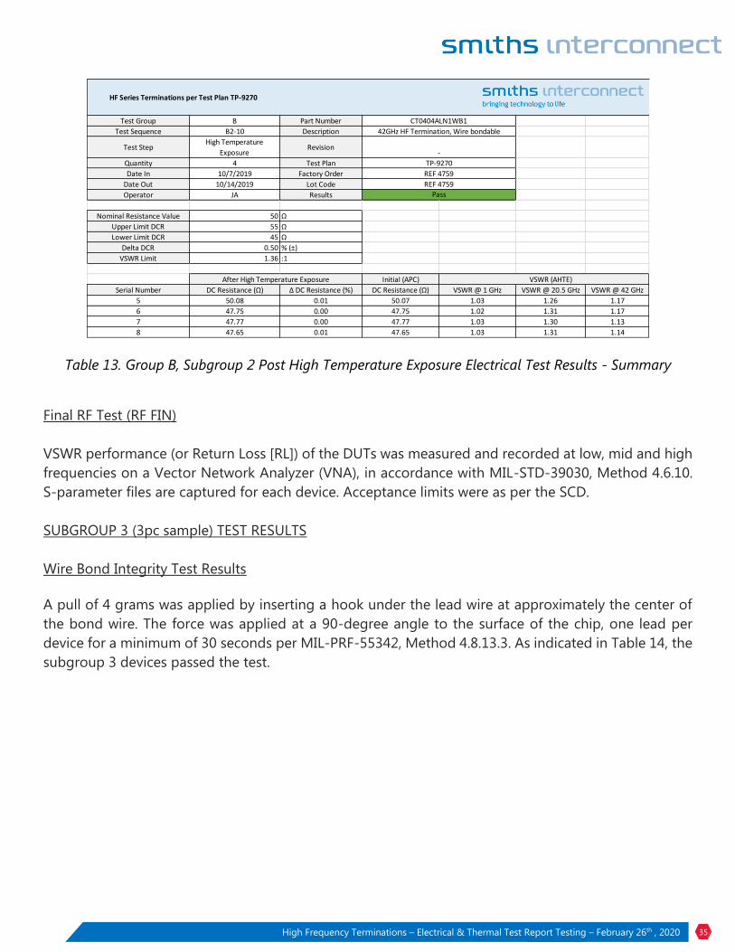
High Temperature Exposure Test Results
The devices were subjected to 150°C ±5°C for a period of 100 hours ±4 hours per MIL-PRF-55342,
Method 4.8.7.
DC resistance between the input port and the ground path (Figure 25) was measured and recorded in
accordance with MIL-STD-202, Method 303. Acceptance limits were as per the SCD plus DC resistance
0.5 % from the previous electrical test. As shown in Table 13, the 4-sample inspection lot passed the
requirements.
High Frequency Terminations – Electrical & Thermal Test Report Testing – February 26th , 2020 35
Table 13. Group B, Subgroup 2 Post High Temperature Exposure Electrical Test Results - Summary
Final RF Test (RF FIN)
VSWR performance (or Return Loss [RL]) of the DUTs was measured and recorded at low, mid and high
frequencies on a Vector Network Analyzer (VNA), in accordance with MIL-STD-39030, Method 4.6.10.
S-parameter files are captured for each device. Acceptance limits were as per the SCD.
SUBGROUP 3 (3pc sample) TEST RESULTS
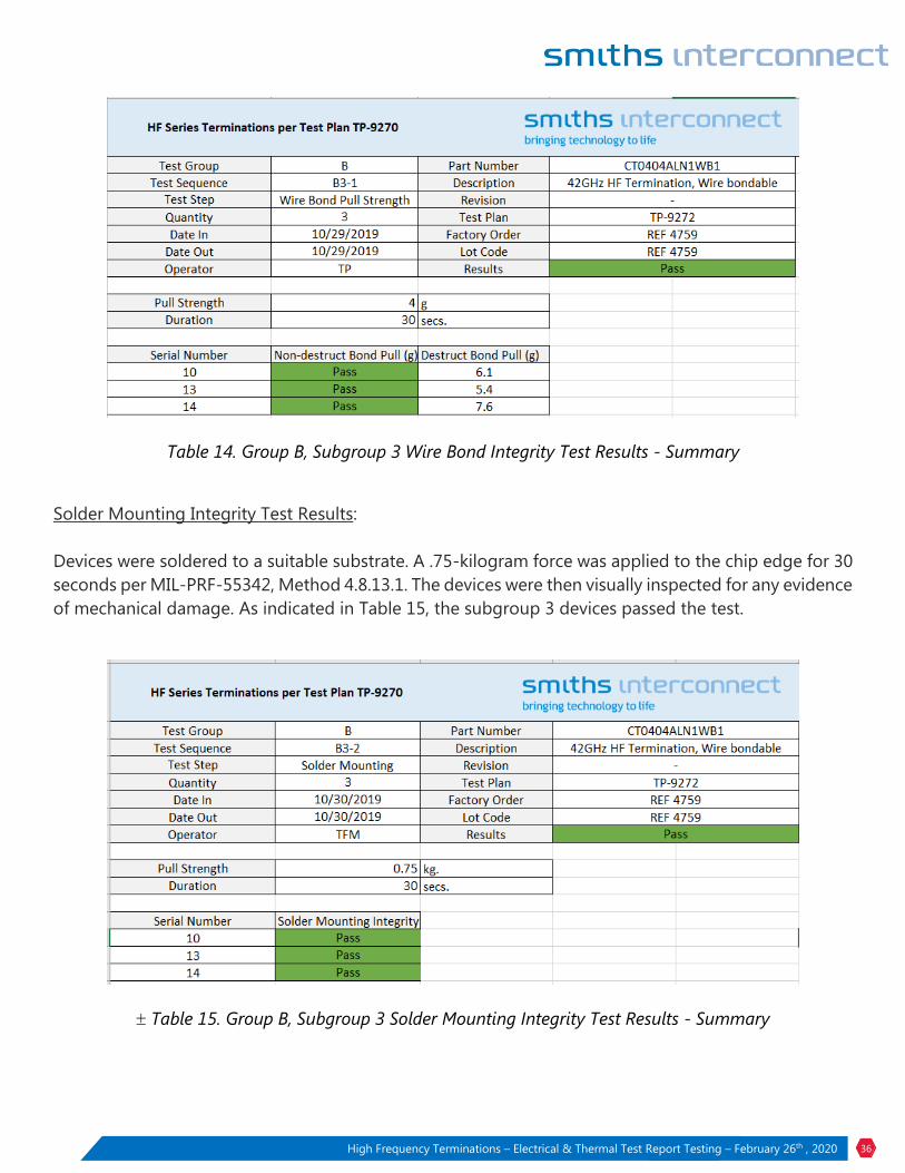
Wire Bond Integrity Test Results
A pull of 4 grams was applied by inserting a hook under the lead wire at approximately the center of
the bond wire. The force was applied at a 90-degree angle to the surface of the chip, one lead per
device for a minimum of 30 seconds per MIL-PRF-55342, Method 4.8.13.3. As indicated in Table 14, the
subgroup 3 devices passed the test.
HF Series Terminations per Test Plan TP-9270
Test Group B Part Number
Test Sequence B2-10 Description
Test StepHigh Temperature
ExposureRevision
Quantity 4 Test Plan
Date In 10/7/2019 Factory Order
Date Out 10/14/2019 Lot Code
Operator JA Results
Nominal Resistance Value 50 Ω
Upper Limit DCR 55 Ω
Lower Limit DCR 45 Ω
Delta DCR 0.50 % (±)
VSWR Limit 1.36 :1
Initial (APC) VSWR (AHTE)
Serial Number DC Resistance (Ω) Δ DC Resistance (%) DC Resistance (Ω) VSWR @ 1 GHz VSWR @ 20.5 GHz VSWR @ 42 GHz
5 50.08 0.01 50.07 1.03 1.26 1.17
6 47.75 0.00 47.75 1.02 1.31 1.17
7 47.77 0.00 47.77 1.03 1.30 1.13
8 47.65 0.01 47.65 1.03 1.31 1.14
Pass
After High Temperature Exposure
CT0404ALN1WB1
42GHz HF Termination, Wire bondable
-
TP-9270
REF 4759
REF 4759
High Frequency Terminations – Electrical & Thermal Test Report Testing – February 26th , 2020 36
Table 14. Group B, Subgroup 3 Wire Bond Integrity Test Results - Summary
Solder Mounting Integrity Test Results:
Devices were soldered to a suitable substrate. A .75-kilogram force was applied to the chip edge for 30
seconds per MIL-PRF-55342, Method 4.8.13.1. The devices were then visually inspected for any evidence
of mechanical damage. As indicated in Table 15, the subgroup 3 devices passed the test.
Table 15. Group B, Subgroup 3 Solder Mounting Integrity Test Results - Summary

High Frequency Terminations – Electrical & Thermal Test Report Testing – February 26th , 2020 37
GROUP C INSPECTION (4 samples):
Group C inspection was conducted on randomly selected samples that have been previously subjected
to Group A Inspection.
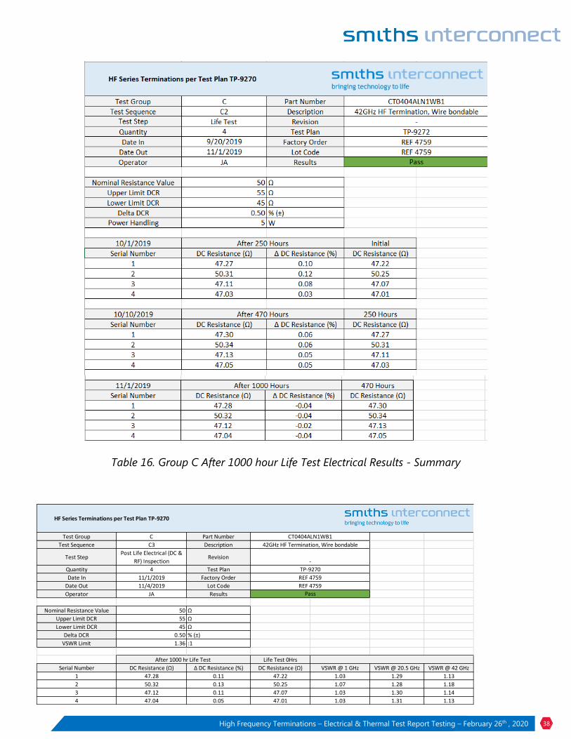
Life Test (1000 hr Burn-In):
The devices were subjected to the maximum input power specified in the SCD by applying the
equivalent DC voltage to properly mounted devices on a suitable heat sink for a total of 1000 +48/-0
hours at 70°C base temp. The power was continuously increased until the maximum power and base
temp were achieved. Electrical (DC Resistance) measurements were made and recorded after 250 +48/-
0, 500 +48/-0, and 1000 +48/-0 hours. Acceptance limits were as per the SCD plus DC Resistance 0.5
% from after previous electrical test.
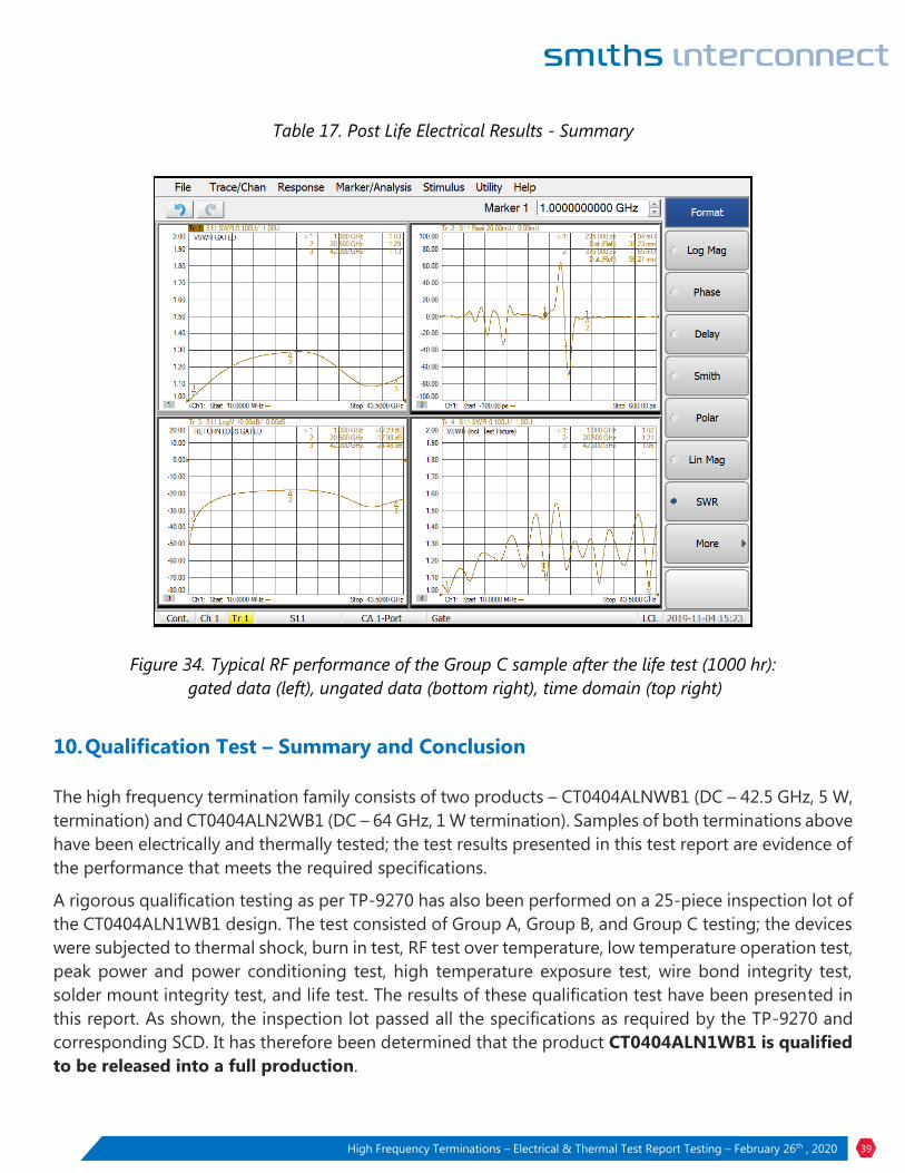
VSWR performance (or Return Loss) of the DUTs was measured and recorded at low, mid and high
frequencies on a Vector Network Analyzer (VNA), in accordance with MIL-STD-39030, Method 4.6.10.
S-parameter files are captured for each device. Acceptance limits as per the SCD.
High Frequency Terminations – Electrical & Thermal Test Report Testing – February 26th , 2020 38
Table 16. Group C After 1000 hour Life Test Electrical Results - Summary
HF Series Terminations per Test Plan TP-9270
Test Group C Part Number
Test Sequence C3 Description
Test StepPost Life Electrical (DC &
RF) InspectionRevision
Quantity 4 Test Plan
Date In 11/1/2019 Factory Order
Date Out 11/4/2019 Lot Code
Operator JA Results
Nominal Resistance Value 50 Ω
Upper Limit DCR 55 Ω
Lower Limit DCR 45 Ω
Delta DCR 0.50 % (±)
VSWR Limit 1.36 :1
Life Test 0Hrs
Serial Number DC Resistance (Ω) Δ DC Resistance (%) DC Resistance (Ω) VSWR @ 1 GHz VSWR @ 20.5 GHz VSWR @ 42 GHz
1 47.28 0.11 47.22 1.03 1.29 1.13
2 50.32 0.13 50.25 1.07 1.28 1.18
3 47.12 0.11 47.07 1.03 1.30 1.14
4 47.04 0.05 47.01 1.03 1.31 1.13
Pass
After 1000 hr Life Test
CT0404ALN1WB1
42GHz HF Termination, Wire bondable
-
TP-9270
REF 4759
REF 4759
High Frequency Terminations – Electrical & Thermal Test Report Testing – February 26th , 2020 39
Table 17. Post Life Electrical Results - Summary
Figure 34. Typical RF performance of the Group C sample after the life test (1000 hr):
gated data (left), ungated data (bottom right), time domain (top right)
10. Qualification Test – Summary and Conclusion
The high frequency termination family consists of two products – CT0404ALNWB1 (DC – 42.5 GHz, 5 W,
termination) and CT0404ALN2WB1 (DC – 64 GHz, 1 W termination). Samples of both terminations above
have been electrically and thermally tested; the test results presented in this test report are evidence of
the performance that meets the required specifications.
A rigorous qualification testing as per TP-9270 has also been performed on a 25-piece inspection lot of
the CT0404ALN1WB1 design. The test consisted of Group A, Group B, and Group C testing; the devices
were subjected to thermal shock, burn in test, RF test over temperature, low temperature operation test,
peak power and power conditioning test, high temperature exposure test, wire bond integrity test,
solder mount integrity test, and life test. The results of these qualification test have been presented in
this report. As shown, the inspection lot passed all the specifications as required by the TP-9270 and
corresponding SCD. It has therefore been determined that the product CT0404ALN1WB1 is qualified
to be released into a full production.
High Frequency Terminations – Electrical & Thermal Test Report Testing – February 26th , 2020 40
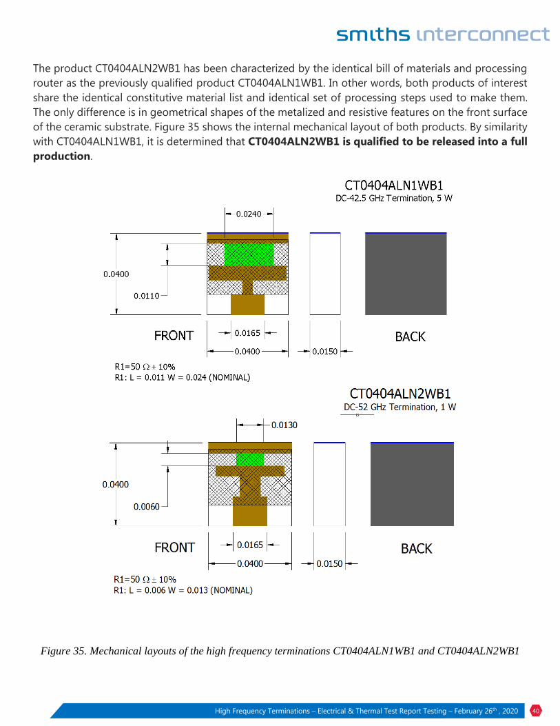
The product CT0404ALN2WB1 has been characterized by the identical bill of materials and processing
router as the previously qualified product CT0404ALN1WB1. In other words, both products of interest
share the identical constitutive material list and identical set of processing steps used to make them.
The only difference is in geometrical shapes of the metalized and resistive features on the front surface
of the ceramic substrate. Figure 35 shows the internal mechanical layout of both products. By similarity
with CT0404ALN1WB1, it is determined that CT0404ALN2WB1 is qualified to be released into a full
production.
Figure 35. Mechanical layouts of the high frequency terminations CT0404ALN1WB1 and CT0404ALN2WB1