Embed Size (px)
Citation preview

c h a p t e r
4
The von Neumann Model
We are now ready to raise our level of abstraction another notch. We will build on the logic structures that we studied in Chapter 3, both decision elements and storage elements, to construct the basic computer model first proposed by John von Neumann in 1946.
4.1 Basic Components To get a task done by a computer, we need two things: a computer program that specifies what the computer must to do to complete the task, and the computer itself that is to carry out the task.
A computer program consists of a set of instructions, each specifying a well-defined piece of work for the computer to carry out. The instruction is the smallest piece of work specified in a computer program. That is, the computer either carries out the work specified by an instruction or it does not. The computer does not have the luxury of carrying out a piece of an instruction.
John von Neumann proposed a fundamental model of a computer for process-ing computer programs in 1946. Figure 4.1 shows its basic components. We have taken a little poetic license and added a few of our own minor embellishments to von Neumann's original diagram. The von Neumann model consists of five parts: memory; a processing unit, input, output, and a control unit. The computer program is contained in the computer's memory. The control of the order in which the instructions are carried out is performed by the control unit.
We will describe each of the five parts of the von Neumann model.

121 chapter 4 The von Neumann Model
MEMORY
INPUT
MAR MDR
OUTPUT
* Keyboard * Mouse * Scanner * Card reader * Disk
PROCESSING UNIT
ALU TEMP
* Monitor * Printer * LED * Disk
CONTROL UNIT
a PC
IR
Figure 4 . 1 The von Neumann model, overall block diagram
4.1.1 Memory Recall that in Chapter 3 we examined a simple 22-by-3-bit memory that was con-structed out of gates and latches. A more realistic memory for one of today's computer systems is 228 by 8 bits. That is, a typical memory in today's world of computers consists of 228 distinct memory locations, each of which is capa-ble of storing 8 bits of information. We say that such a memory has an address space of 228 uniquely identifiable locations, and an addressability of 8 bits. We refer to such a memory as a 256-megabyte memory (abbreviated, 256MB). The "256 mega" refers to the 228 locations, and the "byte" refers to the 8 bits stored in each location. The term byte is, by definition, the word used to describe 8 bits, much the way gallon describes four quarts.
We note (as we will note again and again) that with k bits, we can represent uniquely 2k items. Thus, to uniquely identify 228 memory locations, each loca-tion must have its own 28-bit address. In Chapter 5, we will begin the complete definition of the instruction set architecture (ISA) of the LC-3 computer. We will see that the memory address space of the LC-3 is 216, and the addressability is 16 bits.
Recall from Chapter 3 that we access memory by providing the address from which we wish to read, or to which we wish to write. To read the contents of a mem-ory location, we first place the address of that location in the memory's address register ( M A R ) , and then interrogate the computer's memory. The information

4.1 Basic Components
000
001
010
011 100 101
110
111
Figure 4.2 Location 6 contains the value 4; location 4 contains the value 6
stored in the location having that address will be placed in the memory's data register (MDR). To write (or store) a value in a memory location, we first write the address of the memory location in the MAR, and the value to be stored in the MDR. We then interrogate the computer's memory with the Write Enable signal asserted. The information contained in the MDR will be written into the memory location whose address is in the MAR.
Before we leave the notion of memory for the moment, let us again emphasize the two characteristics of a memory location: its address and what is stored there. Figure 4.2 shows a representation of a memory consisting of eight locations. Its addresses are shown at the left, numbered in binary from 0 to 7. Each location contains 8 bits of information. Note that the value 6 is stored in the memory location whose address is 4, and the value 4 is stored in the memory location whose address is 6. These represent two very different situations.
Finally, an analogy comes to mind: the post office boxes in your local post office. The box number is like the memory location's address. Each box number is unique. The information stored in the memory location is like the letters contained in the post office box. As time goes by, what is contained in the post office box at any particular moment can change. But the box number remains the same. So, too, with each memory location. The value stored in that location can be changed, but the location's memory address remains unchanged.
4.1.2 Processing Unit The actual processing of information in the computer is carried out by the processing unit. The processing unit in a modern computer can consist of many sophisticated complex functional units, each performing one particular operation (divide, square root, etc.). The simplest processing unit, and the one normally thought of when discussing the basic von Neumann model, is the ALU. ALU is the abbreviation for Arithmetic and Logic Unit, so called because it is usually capable of performing basic arithmetic functions (like ADD and SUBTRACT) and basic logic operations (like bit-wise AND, OR, and NOT that we have already studied in Chapter 2). As we will see in Chapter 5, the LC-3 has an ALU, which can perform ADD, AND, and NOT operations.
The size of the quantities normally processed by the ALU is often referred to as the word length of the computer, and each element is referred to as a word. In
00000110
00000100
100 chapter 4 The von Neumann Model
the LC-3, the ALU processes 16-bit quantities. We say the LC-3 has a word length of 16 bits. Each ISA has its own word length, depending on the intended use of the computer. Most microprocessors today that are used in PCs or workstations have a word length of either 32 bits (as is the case with Intel's Pentium IV) or 64 bits (as is the case with Sun's SPARC-V9 processors and Intel's Itanium processor). For some applications, like the microprocessors used in pagers, VCRs, and cellular telephones, 8 bits are usually enough. Such microprocessors, we say, have a word length of 8 bits.
It is almost always the case that a computer provides some small amount of storage very close to the ALU to allow results to be temporarily stored if they will be needed to produce additional results in the near future. For example, if a computer is to calculate (A + B) • C, it could store the result of A + B in memory, and then subsequently read it in order to multiply that result by C. However, the time it takes to access memory is long compared to the time it takes to perform the ADD or MULTIPLY. Almost all computers, therefore, have temporary storage for storing the result of A + B in order to avoid the unnecessarily longer access time that would be necessary when it came time to multiply. The most common form of temporary storage is a set of registers, like the register described in Section 3.4.3. Typically, the size of each register is identical to the size of values processed by the ALU, that is, they each contain one word. The LC-3 has eight registers (R0, Rl, . . . R7), each containing 16 bits. The SPARC-V9 ISA has 32 registers (R0, R l , . . . R31), each containing 64 bits.
4.1.3 Input and Output In order for a computer to process information, the information must get into the computer. In order to use the results of that processing, those results must be displayed in some fashion outside the computer. Many devices exist for the purposes of input and output. They are generically referred to in computer jar-gon as peripherals because they are in some sense accessories to the processing function. Nonetheless, they are no less important.
In the LC-3 we will have the two most basic of input and output devices. For input, we will use the keyboard; for output, we will use the monitor.
There are, of course, many other input and output devices in computer systems today. For input we have among other things the mouse, digital scanners, and floppy disks. For output we have among other things printers, LED displays, and disks. In the old days, much input and output was carried out by punched cards. Fortunately, for those who would have to lug boxes of cards around, the use of punched cards has largely disappeared.
4.1.4 Control Unit The control unit is like the conductor of an orchestra; it is in charge of making all the other parts play together. As we will see when we describe the step-by-step process of executing a computer program, it is the control unit that keeps track of both where we are within the process of executing the program and where we are in the process of executing each instruction.
4.2 The LC-3: An Example von Neumann Machine 101
To keep track of which instruction is being executed, the control unit has an instruction register to contain that instruction. To keep track of which instruction is to be processed next, the control unit has a register that contains the next instruction's address. For historical reasons, that register is called the program counter (abbreviated PC), although a better name for it would be the instruction pointer, since the contents of this register are, in some sense, "pointing" to the next instruction to be processed. Curiously, Intel does in fact call that register the instruction pointer, but the simple elegance of that name has not caught on.
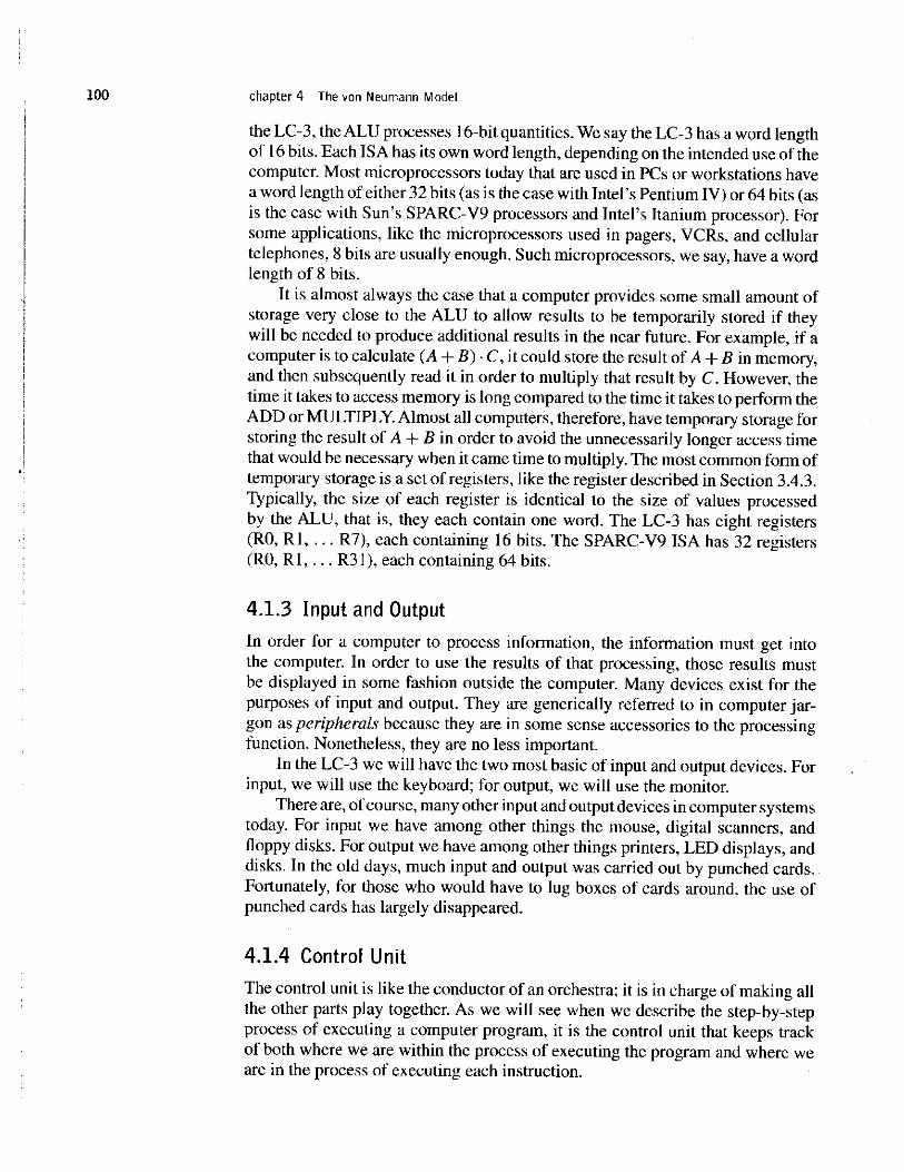
4.2 The LC-3: On Example von Neumann Machine In Chapter 5, we will introduce in detail the LC-3, a simple computer that we will study extensively. We have already shown you its data path in Chapter 3 (Figure 3.33) and identified several of its structures in Section 4.1. In this sec-tion, we will pull together all the parts of the LC-3 we need to describe it as a von Neumann computer (see Figure 4.3). We constructed Figure 4.3 by start-ing with the LC-3's full data path (Figure 3.33) and removing all elements that are not essential to pointing out the five basic components of the von Neumann model.
Note that there are two kinds of arrowheads in Figure 4.3: filled-in and not-filled-in. Filled-in arrowheads denote data elements that flow along the cor-responding paths. Not-filled-in arrowheads denote control signals that control the processing of the data elements. For example, the box labeled ALU in the pro-cessing unit processes two 16-bit values and produces a 16-bit result. The two sources and the result are all data, and are designated by filled-in arrowheads. The operation performed on those two 16-bit data elements (it is labeled ALUK) is part of the control—therefore, a not-filled-in arrowhead.
MEMORY consists of the storage elements, along with the MAR for addressing individual locations and the MDR for holding the contents of a memory location on its way to/from the storage. Note that the MAR contains 16 bits, reflecting the fact that the memory address space of the LC-3 is 216 memory locations. The MDR contains 16 bits, reflecting the fact that each memory location contains 16 bits—that is, that the LC-3 is 16-bit addressable.
INPUT/OUTPUT consists of a keyboard and a monitor. The simplest keyboard requires two registers, a data register (KBDR) for holding the ASCII codes of keys struck, and a status register (KBSR) for maintaining status information about the keys struck. The simplest monitor also requires two registers, one (DDR) for holding the ASCII code of something to be displayed on the screen, and one (DSR) for maintaining associated status information. These input and output registers will be discussed in more detail in Chapter 8.
T H E P R O C E S S I N G U N I T consists of a functional unit that can perform arithmetic and logic operations (ALU) and eight registers (R0, . . . R7) for storing temporary values that will be needed in the near future as operands

1 0 2 chapter 4 The von Neumann Model
PROCESSOR BUS I GatePC
i GateMDR
16/|
LD.MDR —
16
LD.PC —*> PC
H PCMUX \ +1
16
CLK
IR
/ 16
R —l
LD.IR
FINITE STATE
MACHINE
CONTROL UNIT
16
MDR MEM.EN, R.W
4 MAR LD.MAR
16
LD.REG-
SR2
R E G F I L E
SR2 SR1 O U T O U T
/ / 16
£ ALUK NT
ALU
PROCESSING UNIT
GateALU
T 4
KBDR
KBSR
DDR
DSR
MEMORY INPUT OUTPUT
Figure 4.3 T h e L C - 3 as a n e x a m p l e o f t h e v o n N e u m a n n m o d e l
for subsequent instructions. The LC-3 ALU can perform one arithmetic operation (addition) and two logical operations (bitwise AND and bitwise complement).
THE CONTROL UNIT consists of all the structures needed to manage the processing that is carried out by the computer. Its most important structure is the finite state machine, which directs all the activity. Recall the finite state machines in Section 3.6. Processing is carried out step by step, or rather, clock cycle by clock cycle. Note the CLK input to the finite state machine in Figure 4.3. It specifies how long each clock cycle lasts. The
4.3 Instruction Processing 103
instruction register (IR) is also an input to the finite state machine since what LC-3 instruction is being processed determines what activities must be carried out. The program counter (PC) is also a part of the control unit; it keeps track of the next instruction to be executed after the current instruction finishes.
Note that all the external outputs of the finite state machine in Figure 4.3 have arrowheads that are not filled in. These outputs control the processing throughout the computer. For example, one of these outputs (two bits) is ALUK, which controls the operation performed in the ALU (add, and, or not) during the current clock cycle. Another output is GateALU, which determines whether or not the output of the ALU is provided to the processor bus during the current clock cycle.
The complete description of the data path, control, and finite state machine for one implementation of the LC-3 is the subject of Appendix C.
4.3 Instruction Processing The central idea in the von Neumann model of computer processing is that the program and data are both stored as sequences of bits in the computer's memory, and the program is executed one instruction at a time under the direction of the control unit.
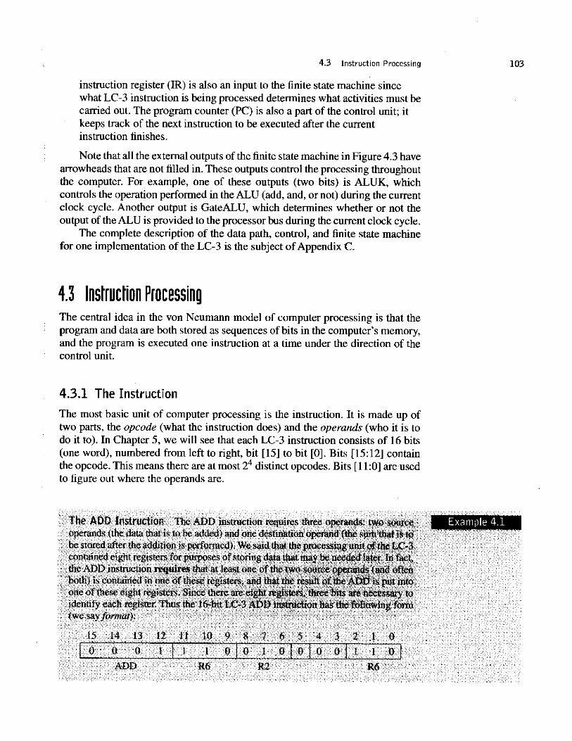
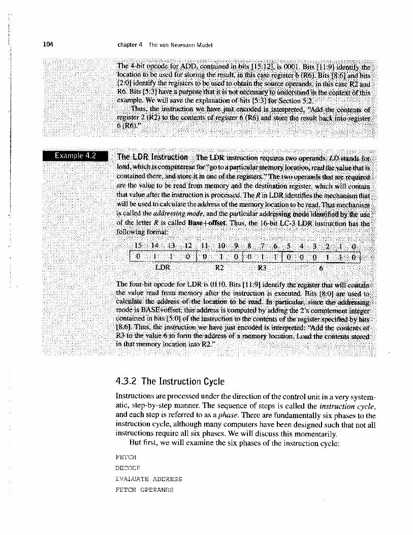
4.3.1 The Instruction The most basic unit of computer processing is the instruction. It is made up of two parts, the opcode (what the instruction does) and the operands (who it is to do it to). In Chapter 5, we will see that each LC-3 instruction consists of 16 bits (one word), numbered from left to right, bit [15] to bit [0]. Bits [15:12] contain the opcode. This means there are at most 24 distinct opcodes. Bits [11:0] are used to figure out where the operands are.
The ADD Instruction The ADD instruction requires three operands: two source operands (the data that is to he added) and one destination operand (the sum that is to be stored after the addition is performed). We said that the processing unit of the LC-3 contained eight registers for purposes of storing data that may be needed later. In fact, the ADD instruction requires that at least one of the two source operands (and often both) is contained in one of these registers, and that the result of the ADD is put into one of these eight registers. Since there are eight registers, three hits are necessary to identify each register. Thus the 16-bit LC-3 ADD instruction has the following form (we say format):
Examp le 4 . 1
15 14 13 I 0 0 ADD
11 10 <)
R6
6 0 I 0
R2
1 0 0 0 | 1 I 0 |
R6
104 chapter 4 The von Neumann Model
The 4-hii opcode lor ADD. contained in hits 115:121. is 0001. Hits 1 1 i d e n t i f y the location Lo he used for storing ihe result, in this case register 6 (R6). Bits |K:ft| and hits 12:0| identify the regislers lo he used lo obtain Ihe source operands, in this case R2 and Rft. Mils 15:31 have a purpose that it is not necessary lo understand in the context of this example. We will save Ihe explanation of hils [5:31 for Section 5.2.
Thus, the instruction we have just encoded is interpreted, "Add the contents of register 2 (R2) to the contents of register 6 (Rft) and store the result back into register 0(K6i;
The LDR Instruction The LDR instruction requires two operands. LD stands for load, which is computerese for "go to a particular memory location, read the value that is contained there, and store it in one of the registers." The two operands that are required are the value to be read from memory and the destination register, which will contain that value after the instruction is processed. The R in LDR identifies the mechanism that will be used to calculate the address of the memoiy location to be read. That mechanism is called the addressing mode, and the particular addressing mode identified by the use of the letter R is called Base+offset. Thus, the 16-bit LC-3 LDR instruction has the following format:
15 14 13 12 11 10 9 8 7 6 5 4 3 2 1 0 0 1 1 0 0 1 0 0 1 1 0 0 0 1 1 0
LDR R2 R3 6
The four-bit opcode for LDR is 0110. Bits [11:9) identify the register that will contain the value read from memory after the instruction is executed. Bits [8:0] are used to calculate the address of the location to be read. In particular, since the addressing mode is BASE+offset, this address is computed by adding the 2's complement integer contained in bits [5:0| of the instruction to the contents of the register specified by bits 18:6]. Thus, the instruction we have just encoded is interpreted: "Add the contents of R3 to the value 6 to form the address of a memory location. Load the contents stored in that memory location into R2."
4.3.2 The Instruction Cycle Instructions are processed under the direction of the control unit in a very system-atic, step-by-step manner. The sequence of steps is called the instruction cycle, and each step is referred to as a phase. There are fundamentally six phases to the instruction cycle, although many computers have been designed such that not all instructions require all six phases. We will discuss this momentarily.
But first, w e will examine the six phases of the instruction cycle:
FETCH
DECODE
EVALUATE ADDRESS
FETCH OPERANDS

4.3 Instruction Processing 105
EXECUTE
STORE RESULT
The process is as follows (again refer to Figure 4.3, our simplified version of the LC-3 data path):
FETCH The FETCH phase obtains the next instruction from memory and loads it into the instruction register (IR) of the control unit. Recall that a computer program consists of a collection of instructions, that each instruction is represented by a sequence of bits, and that the entire program (in the von Neumann model) is stored in the computer's memory. In order to carry out the work of the next instruction, we must first identify where it is. The program counter (PC) contains the address of the next instruction. Thus, the FETCH phase takes multiple steps:
First the MAR is loaded with the contents of the PC.
Next, the memory is interrogated, which results in the next instruction being placed by the memory into the MDR.
Finally, the IR is loaded with the contents of the MDR.
We are now ready for the next phase, decoding the instruction. However, when the instruction cycle is complete, and we wish to fetch the next instruction, we would like the PC to contain the address of the next instruction. Therefore, one more step the FETCH phase must perform is to increment the PC. In that way, at the completion of the execution of this instruction, the FETCH phase of the next instruction will load into IR the contents of the next memory location, provided the execution of the current instruction does not involve changing the value in the PC.
The complete description of the FETCH phase is as follows:
Step 1: Load the MAR with the contents of the PC, and simultaneously increment the PC.
Step 2: Interrogate memory, resulting in the instruction being placed in the MDR.
Step 3: Load the IR with the contents of the MDR.
Each of these steps is under the direction of the control unit, much like, as we said previously, the instruments in an orchestra are under the control of a conductor's baton. Each stroke of the conductor's baton corresponds to one machine cycle. We will see in Section 4.4.1 that the amount of time taken by each machine cycle is one clock cycle. In fact, we often use the two terms interchangeably. Step 1 takes one machine cycle. Step 2 could take one machine cycle, or many machine cycles, depending on how long it takes to access the computer's memory. Step 3 takes one machine cycle. In a modern digital computer, a machine cycle takes a very small fraction of a second. Indeed, a 3.3-GHz Intel Pentium IV completes 3.3. billion

106 chapter 4 The von Neumann Model
machine cycles (or clock cycles) in one second. Said another way, one machine cycle (or clock cycle) takes 0.303 billionths of a second (0.303 nanoseconds). Recall that the light bulb that is helping you read this text is switching on and off at the rate of 60 times a second. Thus, in the time it takes a light bulb to switch on and off once, today's computers can complete 55 million machine cycles!
DECODE The DECODE phase examines the instruction in order to figure out what the microarchitecture is being asked to do. Recall the decoders we studied in Chap-ter 3. In the LC-3, a 4-to-16 decoder identifies which of the 16 opcodes is to be processed. Input is the four-bit opcode IR[15:12]. The output line asserted is the one corresponding to the opcode at the input. Depending on which output of the decoder is asserted, the remaining 12 bits identify what else is needed to process that instruction.
EVALUATE ADDRESS This phase computes the address of the memory location that is needed to process the instruction. Recall the example of the LDR instruction: The LDR instruction causes a value stored in memory to be loaded into a register. In that example, the address was obtained by adding the value 6 to the contents of R3. This calculation was performed during the EVALUATE ADDRESS phase.
FETCH OPERANDS This phase obtains the source operands needed to process the instruction. In the LDR example, this phase took two steps: loading MAR with the address calculated in the EVALUATE ADDRESS phase, and reading memory, which resulted in the source operand being placed in MDR.
In the ADD example, this phase consisted of obtaining the source operands from R2 and R6. (In most current microprocessors, this phase [for the ADD instruction] can be done at the same time the instruction is being decoded. Exactly how we can speed up the processing of an instruction in this way is a fascinating subject, but one we are forced to leave for later in your education.)
EXECUTE This phase carries out the execution of the instruction. In the ADD example, this phase consisted of the single step of performing the addition in the ALU.
STORE RESULT The final phase of an instruction's execution. The result is written to its designated destination.
Once the sixth phase (STORE RESULT) has been completed, the control unit begins anew the instruction cycle, starting from the top with the FETCH phase.

4.4 Changing the Sequence of Execution 107
Since the PC was updated during the previous instruction cycle, it contains at this point the address of the instruction stored in the next sequential memory location. Thus the next sequential instruction is fetched next. Processing continues in this way until something breaks this sequential flow.
ADD leax I, edx This is an example of an Intel x86 instruction that requires all six phases of the instruction cycle. All instructions require the first two phases, FETCH and DECODE. This instruction uses the eax register to calculate the address of a memory location (EVALUATE ADDRESS). The contents of that memory location are then read (FETCH OPERAND), added to the contents of the edx register (EXECUTE), and the result written into the memory location that origiuallx contained the lirst source .i|»cr;md (STORE RESULT).
The I.C-3 ADD and LDR instructions do not require all six phases. In particular, the ADD instruction does not require an EVALUATE ADDRESS phase. The LDR instruction does not require an EXECUTE phase.
4.4 Changing The Sequence of Execufion Everything we have said thus far suggests that a computer program is executed in sequence. That is, the first instruction is executed, then the second instruction is executed, followed by the third instruction, and so on.
We have identified two types of instructions, the ADD, which is an exam-ple of an operate instruction in that it processes data, and the LDR, which is an example of a data movement instruction in that it moves data from one place to another. There are other examples of both operate instructions and data move-ment instructions, as we will discover in Chapter 5 when we study the LC-3 in detail.
There is a third type of instruction, the control instruction, whose purpose is to change the sequence of instruction execution. For example, there are times, as we shall see, when it is desirable to first execute the first instruction, then the second, then the third, then the first again, the second again, then the third again, then the first for the third time, the second for the third time, and so on. As we know, each instruction cycle starts with loading the MAR with the PC. Thus, if we wish to change the sequence of instructions executed, we must change the PC between the time it is incremented (during the FETCH phase of one instruction) and the start of the FETCH phase of the next.
Control instructions perform that function by loading the PC during the EXECUTE phase, which wipes out the incremented PC that was loaded dur-ing the FETCH phase. The result is that, at the start of the next instruction cycle, when the computer accesses the PC to obtain the address of an instruction to fetch, it will get the address loaded during the previous EXECUTE phase, rather than the next sequential instruction in the computer's program.

108 chapter 4 The von Neumann Model
Examp le 4 .5 The J M P Instruction Considerthe LC-3 instruction JMP, whose formal follows. Assume lliis instruction is stored in memory location x36A2.
d 14 3 12 11 10 9 8
0 0 0 0 0 0 JMP
7_ r
R~3 0 0
0 Z ]
The 4-bit opcode for JMP is I KM). Hits |8:ft| specify the register which contains the address of the next instruction to be processed. Thus, the instruction encoded here is interpreted, "I ,oad the PC (during the HXliCUTL phase) with the contents of R3 so that the next instruction processed will be the one at the address obtained from R3."
Processing will go on as follows. I,efs start at the beginning of the instruction cycle, with PC = X.16A2. The FETCH phase results in the IK being loaded with the JMP instruction and the PC updated to contain the address x36A3. Suppose the content of R3 at the start of this instruction is x5446. During the KXIiCUTK phase, the PC is loaded with x544f>. Therefore, in the next instruction cycle, the instruction processed will be the one at address x5446. rather than the one at address x.*f>A3.
4.4.1 Control of the Instruction Cycle We have described the instruction cycle as consisting of six phases, each of which has some number of steps. We also noted that one of the six phases, FETCH, required the three sequential steps of loading the MAR with the contents of the PC, reading memory, and loading the IR with the contents of the MDR. Each step of the FETCH phase, and indeed, each step of every operation in the computer is controlled by the finite state machine in the control unit.
Figure 4.4 shows a very abbreviated part of the state diagram corresponding to the finite state machine that directs all phases of the instruction cycle. As is the case with the finite state machines studied in Section 3.6, each state corresponds to one clock cycle of activity. The processing controlled by each state is described within the node representing that state. The arcs show the next state transitions.
Processing starts with state 1. The FETCH phase takes three clock cycles. In the first clock cycle, the MAR is loaded with the contents of the PC, and the PC is incremented. In order for the contents of the PC to be loaded into the MAR (see Figure 4.3), the finite state machine must assert GatePC and LD.MAR. GatePC connects the PC to the processor bus. LD.MAR, the write enable signal of the MAR register, latches the contents of the bus into the MAR at the end of the current clock cycle. (Latches are loaded at the end of the clock cycle if the corresponding control signal is asserted.)
In order for the PC to be incremented (again, see Figure 4.3), the finite state machine must assert the PCMUX select lines to choose the output of the box labeled +1 and must also assert the LD.PC signal to latch the output of the PCMUX at the end of the current cycle.
The finite state machine then goes to state 2. Here, the MDR is loaded with the instruction, which is read from memory.
In state 3, the data is transferred from MDR to the instruction register (IR). This requires the finite state machine to assert GateMDR and LD.IR, which causes

4.4 Changing the Sequence of Execution 132
To state 1 To state 1 To state 1
Figure 4 . 4 An abbreviated state diagram of the LC-3
the IR to be latched at the end of the clock cycle, concluding the FETCH phase of the instruction.
The DECODE phase takes one cycle. In state 4, using the external input IR, and in particular the opcode bits of the instruction, the finite state machine can go to the appropriate next state for processing instructions depending on the particular opcode in IR[15:12]. Processing continues cycle by cycle until the instruction completes execution, and the next state logic returns the finite state machine to state 1.
As we mentioned earlier in this section, it is sometimes necessary not to execute the next sequential instruction but rather to jump to another location to find the next instruction to execute. As we have said, instructions that change the flow of instruction processing in this way are called control instructions. This can be done very easily by loading the PC during the EXECUTE phase of the control instruction, as in state 63 of Figure 4.4, for example.

110 chapter 4 The von Neumann Model
Appendix C contains a full description of the implementation of the LC-3, including its full state diagram and data path. We will not go into that level of detail in this chapter. Our objective here is to show you that there is nothing magic about the processing of the instruction cycle, and that a properly completed state diagram would be able to control, clock cycle by clock cycle, all the steps required to execute all the phases of every instruction cycle. Since each instruction cycle ends by returning to state 1, the finite state machine can process, cycle by cycle, a complete computet program.
4.5 Stopping [tie Computer From everything we have said, it appears that the computer will continue processing instructions, carrying out the instruction cycle again and again, ad nauseum. Since the computer does not have the capacity to be bored, must this continue until someone pulls the plug and disconnects power to the computer?
Usually, user programs execute under the control of an operating system. UNIX, DOS, MacOS, and Windows NT are all examples of operating systems. Operating systems are just computer programs themselves. So as far as the com-puter is concerned, the instruction cycle continues whether a user program is being processed or the operating system is being processed. This is fine as far as user programs are concerned since each user program terminates with a control instruc-tion that changes the PC to again start processing the operating system—often to initiate the execution of another user program.
But what if we actually want to stop this potentially infinite sequence of instruction cycles? Recall our analogy to the conductor's baton, beating at the rate of millions of machine cycles per second. Stopping the instruction sequencing requires stopping the conductor's baton. We have pointed out many times that there is, inside the computer, a component that corresponds very closely to the conductor's baton. It is called the clock, and it defines the machine cycle. It enables the finite state machine to continue on to the next machine cycle, whether that machine cycle is the next step of the current phase or the first step of the next phase of the instruction cycle. Stopping the instruction cycle requires stopping the clock.
Figure 4.5a shows a block diagram of the clock circuit, consisting primarily of a clock generator and a RUN latch. The clock generator is a crystal oscillator, a piezoelectric device that you may have studied in your physics or chemistry class. For our purposes, the crystal oscillator is a black box (recall our definition of black
Clock 2.9 volts
0 volts
Run
One machine
cycle
Figure 4 . 5 The clock circuit and its control
Exercises 134
box in Section 1.4) that produces the oscillating voltage shown in Figure 4.5b. Note the resemblance of that voltage to the conductor's baton. Every machine cycle, the voltage rises to 2.9 volts and then drops back to 0 volts.
If the RUN latch is in the 1 state (i.e., Q — 1), the output of the clock circuit is the same as the output of the clock generator. If the RUN latch is in the 0 state (i.e., Q = 0), the output of the clock circuit is 0.
Thus, stopping the instruction cycle requires only clearing the RUN latch. Every computer has some mechanism for doing that. In some older machines, it is done by executing a HALT instruction. In the LC-3, as in many other machines, it is done under control of the operating system, as we will see in Chapter 9.
Question: If a HALT instruction can clear the RUN latch, thereby stopping the instruction cycle, what instruction is needed to set the RUN latch, thereby reinitiating the instruction cycle?
Exercises
4.1 Name the five components of the von Neumann model. For each component, state its purpose.
4.2 Briefly describe the interface between the memory and the processing unit. That is, describe the method by which the memory and the processing unit communicate.
4.3 What is misleading about the name program counter? Why is the name instruction pointer more insightful?
4.4 What is the word length of a computer? How does the word length of a computer affect what the computer is able to compute? That is, is it a valid argument, in light of what you learned in Chapter 1, to say that a computer with a larger word size can process more information and therefore is capable of computing more than a computer with a smaller word size?
4.5 The following table represents a small memory. Refer to this table for the following questions.
Address Data 0000 0001 11100100 0011 0001 1111 0000 0010 0101 0010 0110 11110000 0001 0011 0000 0000 0000 0000 0100 0000 0000 0110 0101 0101 0000 0000 0000 0110 0110 1111 1110 1101 0011
0111 0000 0110 1101 1001


![Non Von Neumann Computation (a survey) · Background Backus calls for Non Von Neumann Computation Can programming be liberated from the Von Neumann style [Backus, 1978 ] leads to](https://img.pdfslide.us/doc/110x75/5e78d8422f332c73af0c7ed3/non-von-neumann-computation-a-survey-background-backus-calls-for-non-von-neumann.jpg)


![1.4 [Modelo Von Neumann]](https://img.pdfslide.us/doc/110x75/563db8d4550346aa9a974f43/14-modelo-von-neumann.jpg)