Embed Size (px)
Citation preview
Lithography - Chapter 5
Text Book:Silicon VLSI Technology
Fundamentals, Practice and Modelingg
Authors: J. D. Plummer, M. D. Deal, and P. B. Griffina d G
SILICON VLSI TECHNOLOGYFundamentals, Practice and ModelingBy Plummer, Deal & Griffin
© 2000 by Prentice HallUpper Saddle River NJ
Lithography - Chapter 5
Photolithography (Chap. 1)g p y ( p )• Basic lithography process
– Apply photoresistpp y p– Patterned exposure– Remove photoresist regions
Etch wafer Light– Etch wafer– Strip remaining photoresist
Photoresist
Mask
Substrate
Film deposition Photoresist application
Deposited Film
Exposure
Etch mask
SILICON VLSI TECHNOLOGYFundamentals, Practice and ModelingBy Plummer, Deal & Griffin
© 2000 by Prentice HallUpper Saddle River NJ
2Development Etching Resist removal
Lithography - Chapter 5
Lithography• The ability to print patterns with submicron features
and to place patterns on a silicon substrate with better than 0.1 um precision.
• Lithography is arguably the single most important technology in IC manufacturingtechnology in IC manufacturing– Gains have traditionally been paced by the development of
new lithography tools, masks, photoresist materials, and critical dimension etch processescritical dimension etch processes
• Considerations:– Resolution – Exposure field– Placement accuracy (alignment) – Throughput
SILICON VLSI TECHNOLOGYFundamentals, Practice and ModelingBy Plummer, Deal & Griffin
© 2000 by Prentice HallUpper Saddle River NJ
Throughput– Defect density (mask, photoresist and process)
3
Lithography - Chapter 5
SIA NTRS Lithography
Year of Produc tion 1998 2000 2002 2004 2007 2010 2013 2016 2018
Technolo gy Node (half pitch) 250
nm
180 nm 130 nm 90 nm 65 nm 45 nm 32 nm 22 nm 18 nm
MPU Printed Gate Le ngth 100 nm 70 nm 53 nm 35 nm 25 nm 18 nm 13 nm 10 nm
DRAM Bits/ Chip (Sampl ing) 256M 512M 1G 4G 16G 32G 64G 128G 128G
MPU Transistors/C hip (x106) 550 1100 2200 4400 8800 14,000
Gate C D Control 3 (nm) 3.3 2.2 1.6 1.16 0.8 0.6
Overlay (nm) 32 23 18 12.8 8.8 7.2
Fiel d Size (mm) 22x32 22x32 22x32 22x32 22x32 22x32 22x32 22x32 22x32
Exposure Tec hno logy 248 248 nm 248 nm 193nm 193nm + 193nm 193nm ??? ???Exposure Tec hno logy 248nm
248 nm 248 nm+ RET
193nm+ RET
193nm + RET
193nm + RET
+ H 2O
193nm + RET
+ H 2O
157nm??
??? ???
Data Volume/Mas k lev el (GB) 216 729 1644 3700 8326 12490
• 0.7X in linear dimension every 3 years.• Placement accuracy ≈ 1/3 of feature size.• ≈ 35% of wafer manufacturing costs for lithography
SILICON VLSI TECHNOLOGYFundamentals, Practice and ModelingBy Plummer, Deal & Griffin
© 2000 by Prentice HallUpper Saddle River NJ
4
≈ 35% of wafer manufacturing costs for lithography.• Note the ??? - single biggest uncertainty about the future of the roadmap.
Lithography - Chapter 5
Definitions• Critical Dimensions (CD)
– Dimensions that must be maintained
• CD Control– About 10% of minimum feature size.
Expressed as 3 sigma as three standard deviations of the– Expressed as 3-sigma as three standard deviations of the feature size population must be within the specified 10% of the mean)
Placement or Alignment Accuracy• Placement or Alignment Accuracy• Optical Lithography used through 0.18um to 0.13 um
generation. (described in text)g ( )• X-ray, e-Beam and extreme ultraviolet are options
beyond 0.1 um.
SILICON VLSI TECHNOLOGYFundamentals, Practice and ModelingBy Plummer, Deal & Griffin
© 2000 by Prentice HallUpper Saddle River NJ
5
Lithography - Chapter 5
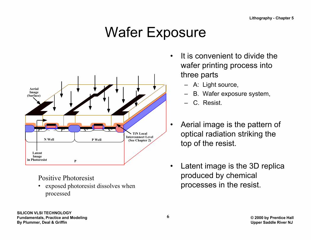
Wafer Exposure• It is convenient to divide the
wafer printing process into three partsthree parts
– A: Light source, – B. Wafer exposure system, – C. Resist.
AerialImage
(Surface)
• Aerial image is the pattern of optical radiation striking the
P+ N+ N+P+TiN Local optical radiation striking the
top of the resist.
• Latent image is the 3D replica
N Well P Well
P
LatentImage
in Photoresist
Interconnect Level(See Chapter 2)
• Latent image is the 3D replica produced by chemical processes in the resist.
Positive Photoresist• exposed photoresist dissolves when
processed
SILICON VLSI TECHNOLOGYFundamentals, Practice and ModelingBy Plummer, Deal & Griffin
© 2000 by Prentice HallUpper Saddle River NJ
6
p
Lithography - Chapter 5
Important Aspects• Masks
– Design, Fabrication, Reuse and Maintenance
• Photoresist– Material, material properties, develop, operation during etch
or mask process post process removalor mask process, post process removal
• Wafer Exposure System– Exposure energy type, focus, linewidth/wavelength,
diff ti ff t (f i i ) d th f fdiffraction effects (fringing), depth of focus
• AllAll– Line width– Alignment
SILICON VLSI TECHNOLOGYFundamentals, Practice and ModelingBy Plummer, Deal & Griffin
© 2000 by Prentice HallUpper Saddle River NJ
7
Lithography - Chapter 5
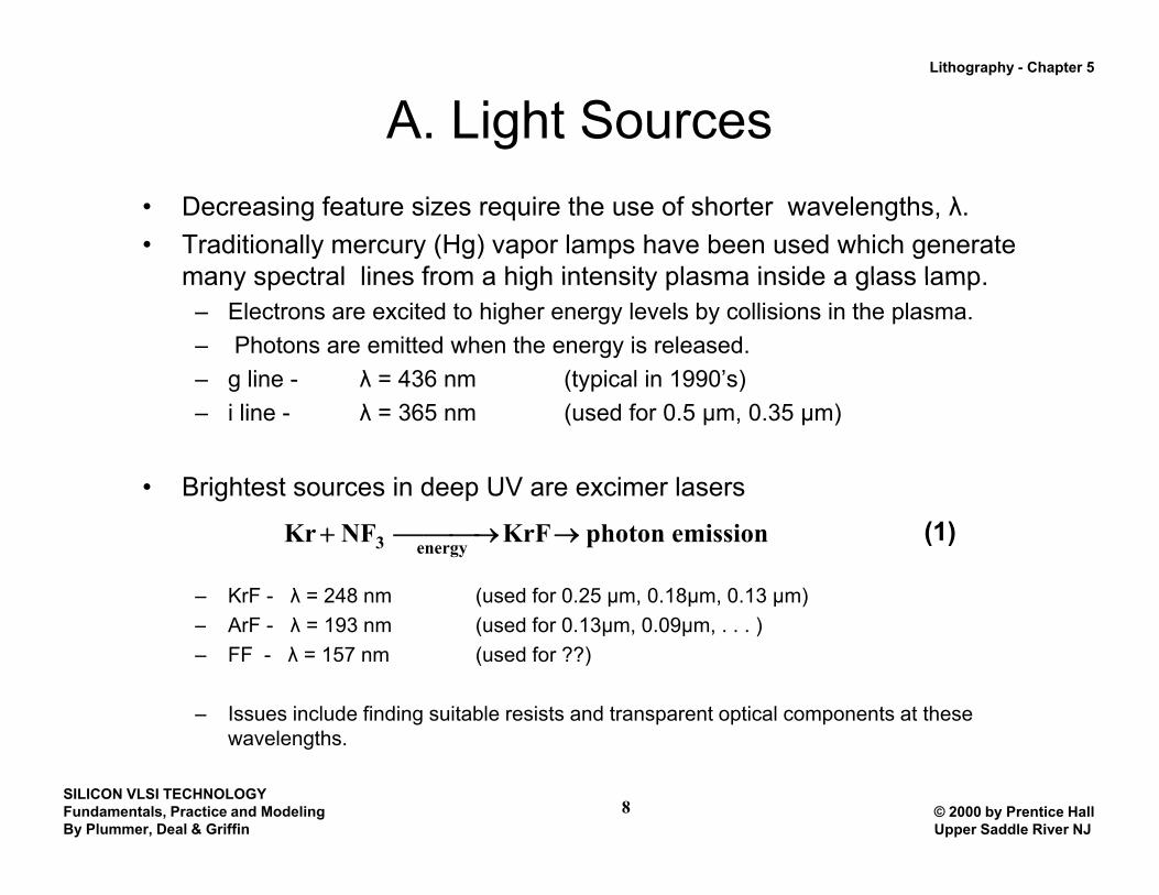
A. Light Sources• Decreasing feature sizes require the use of shorter wavelengths, λ.• Traditionally mercury (Hg) vapor lamps have been used which generate
many spectral lines from a high intensity plasma inside a glass lampmany spectral lines from a high intensity plasma inside a glass lamp. – Electrons are excited to higher energy levels by collisions in the plasma. – Photons are emitted when the energy is released.– g line - λ = 436 nm (typical in 1990’s)g ( yp )– i line - λ = 365 nm (used for 0.5 µm, 0.35 µm)
• Brightest sources in deep UV are excimer lasers
– KrF - λ = 248 nm (used for 0.25 µm, 0.18µm, 0.13 µm)
Kr + NF3 energy
⎯ → ⎯ ⎯ KrF→ photon emission (1)
– ArF - λ = 193 nm (used for 0.13µm, 0.09µm, . . . )– FF - λ = 157 nm (used for ??)
– Issues include finding suitable resists and transparent optical components at these
SILICON VLSI TECHNOLOGYFundamentals, Practice and ModelingBy Plummer, Deal & Griffin
© 2000 by Prentice HallUpper Saddle River NJ
wavelengths.
8
Lithography - Chapter 5
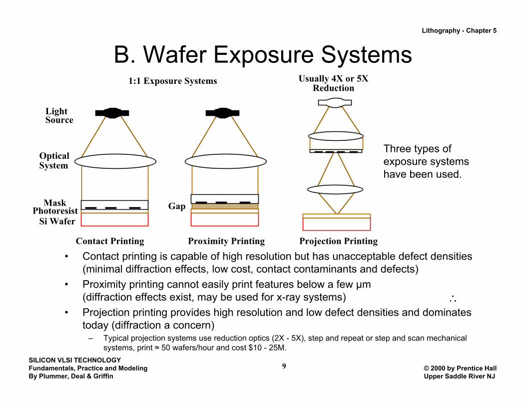
B. Wafer Exposure Systems4
LightSource
1:1 Exposure Systems Usually 4X or 5XReduction
Three types of exposure systems have been used.
OpticalSystem
have been used.
MaskPhotoresist
Si WaferGap
• Contact printing is capable of high resolution but has unacceptable defect densities (minimal diffraction effects, low cost, contact contaminants and defects)
Contact Printing Proximity Printing Projection Printing
• Proximity printing cannot easily print features below a few µm (diffraction effects exist, may be used for x-ray systems)
• Projection printing provides high resolution and low defect densities and dominates today (diffraction a concern)
∴
SILICON VLSI TECHNOLOGYFundamentals, Practice and ModelingBy Plummer, Deal & Griffin
© 2000 by Prentice HallUpper Saddle River NJ
– Typical projection systems use reduction optics (2X - 5X), step and repeat or step and scan mechanical systems, print ≈ 50 wafers/hour and cost $10 - 25M.
9
Lithography - Chapter 5
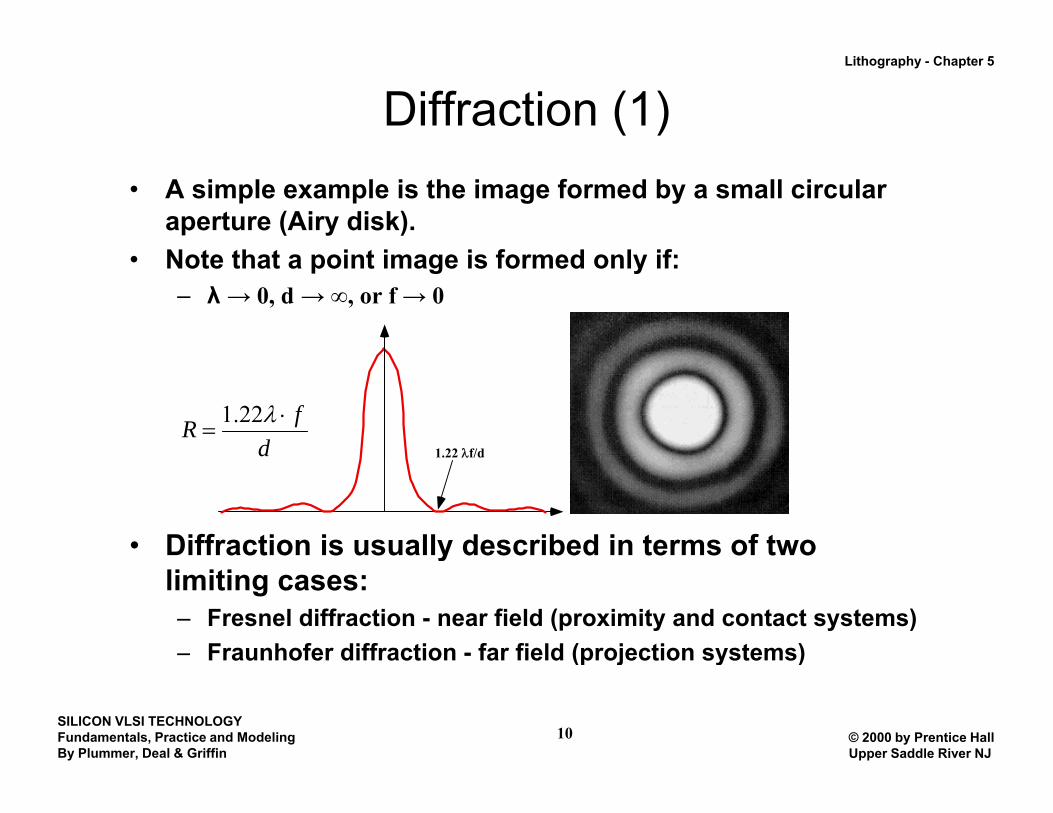
Diffraction (1)• A simple example is the image formed by a small circular
aperture (Airy disk).N t th t i t i i f d l if• Note that a point image is formed only if:– λ→ 0, d → ∞, or f → 0
1.22 λf/ddfR ⋅
=λ22.1
• Diffraction is usually described in terms of two ylimiting cases:– Fresnel diffraction - near field (proximity and contact systems)– Fraunhofer diffraction - far field (projection systems)
SILICON VLSI TECHNOLOGYFundamentals, Practice and ModelingBy Plummer, Deal & Griffin
© 2000 by Prentice HallUpper Saddle River NJ
(p j y )
10
Lithography - Chapter 5
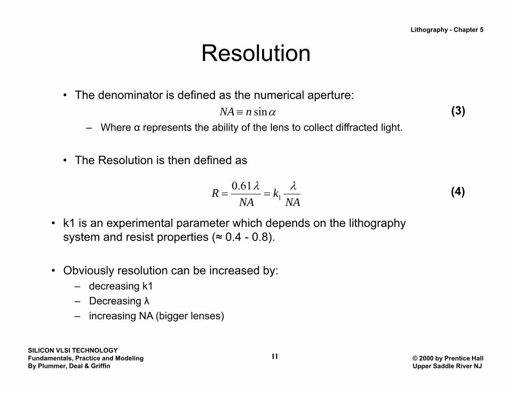
Resolution• The denominator is defined as the numerical aperture:
αsin nNA ≡ (3)– Where α represents the ability of the lens to collect diffracted light.
• The Resolution is then defined as
NAk
NAR λλ 61.0
1== (4)
• k1 is an experimental parameter which depends on the lithography• k1 is an experimental parameter which depends on the lithography system and resist properties (≈ 0.4 - 0.8).
• Obviously resolution can be increased by:Obviously resolution can be increased by: – decreasing k1 – Decreasing λ– increasing NA (bigger lenses)
SILICON VLSI TECHNOLOGYFundamentals, Practice and ModelingBy Plummer, Deal & Griffin
© 2000 by Prentice HallUpper Saddle River NJ
11
Lithography - Chapter 5
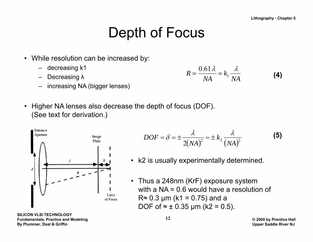
Depth of Focus• While resolution can be increased by:
– decreasing k1 D i λ kR λλ 61.0
1== (4)– Decreasing λ– increasing NA (bigger lenses)
• Higher NA lenses also decrease the depth of focus (DOF)
NAk
NAR 1 (4)
• Higher NA lenses also decrease the depth of focus (DOF). (See text for derivation.)
kDOF λλδ ±± (5)( ) ( )2222 NA
kNA
DOF δ ±=±== (5)
• k2 is usually experimentally determined.
• Thus a 248nm (KrF) exposure system with a NA = 0.6 would have a resolution of R≈ 0 3 µm (k1 = 0 75) and a
SILICON VLSI TECHNOLOGYFundamentals, Practice and ModelingBy Plummer, Deal & Griffin
© 2000 by Prentice HallUpper Saddle River NJ
12
R≈ 0.3 µm (k1 = 0.75) and a DOF of ≈ ± 0.35 µm (k2 = 0.5).
Lithography - Chapter 5
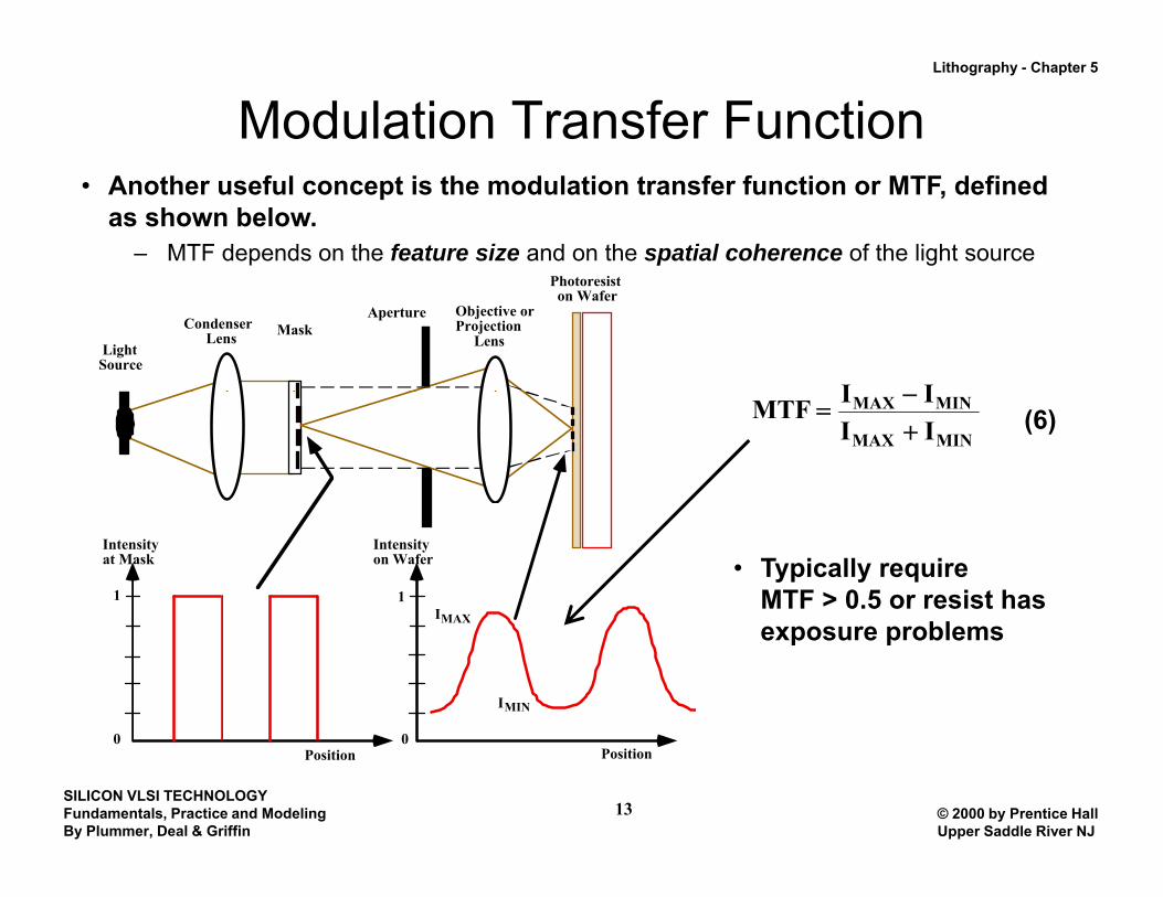
Modulation Transfer Function• Another useful concept is the modulation transfer function or MTF, defined
as shown below.– MTF depends on the feature size and on the spatial coherence of the light source
Photoresist
I I
Aperture
LightSource
Condenser Lens
Objective orProjection Lens
Photoresist on Wafer
Mask
MTF = IMAX − IMIN
IMAX + IMIN(6)
Intensityat Mask
Intensityon Wafer
1 1IMAX
• Typically require MTF > 0.5 or resist has
IMAX
IMIN
exposure problems
SILICON VLSI TECHNOLOGYFundamentals, Practice and ModelingBy Plummer, Deal & Griffin
© 2000 by Prentice HallUpper Saddle River NJ
13
0 0Position Position
Lithography - Chapter 5
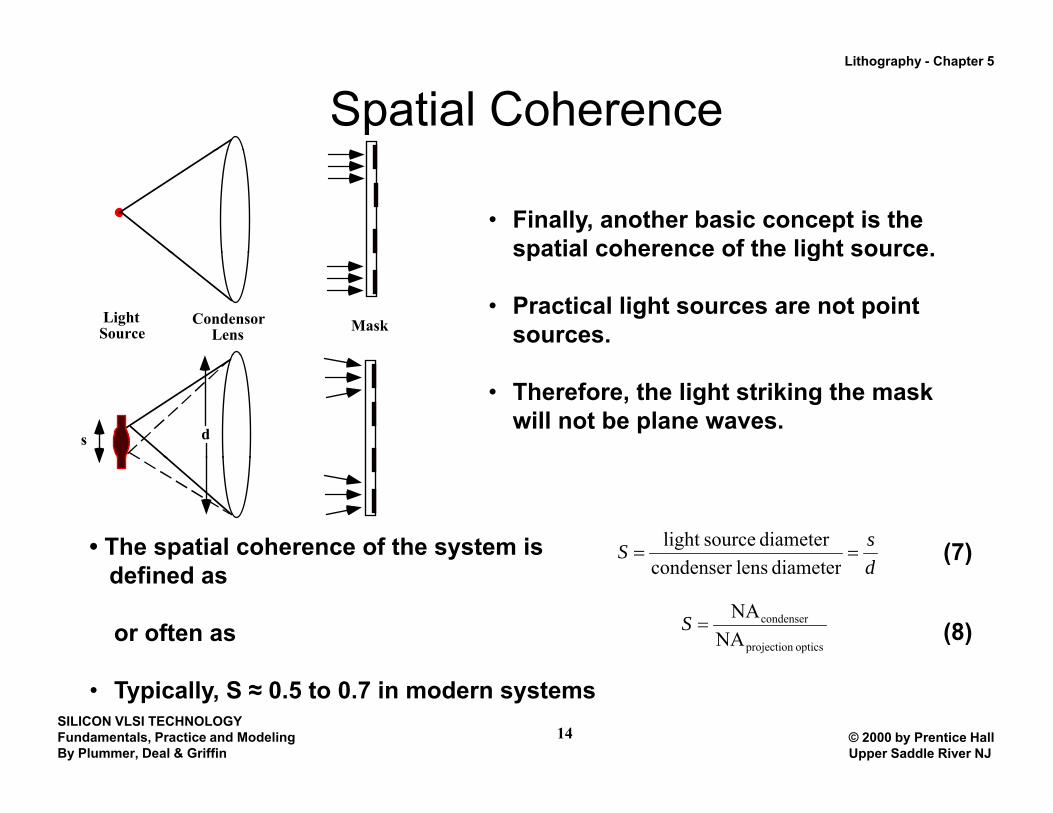
Spatial Coherence
• Finally, another basic concept is the spatial coherence of the light sourcespatial coherence of the light source.
• Practical light sources are not point sources.
LightSource MaskCondensor
Lens
• Therefore, the light striking the mask will not be plane waves.
s d
• The spatial coherence of the system is dsS ==
dilddiameter sourcelight (7)
defined as
or often as
ddiameterlenscondenser ( )
optics projection
condenser
NANA
=S (8)
SILICON VLSI TECHNOLOGYFundamentals, Practice and ModelingBy Plummer, Deal & Griffin
© 2000 by Prentice HallUpper Saddle River NJ
14
• Typically, S ≈ 0.5 to 0.7 in modern systems
Lithography - Chapter 5
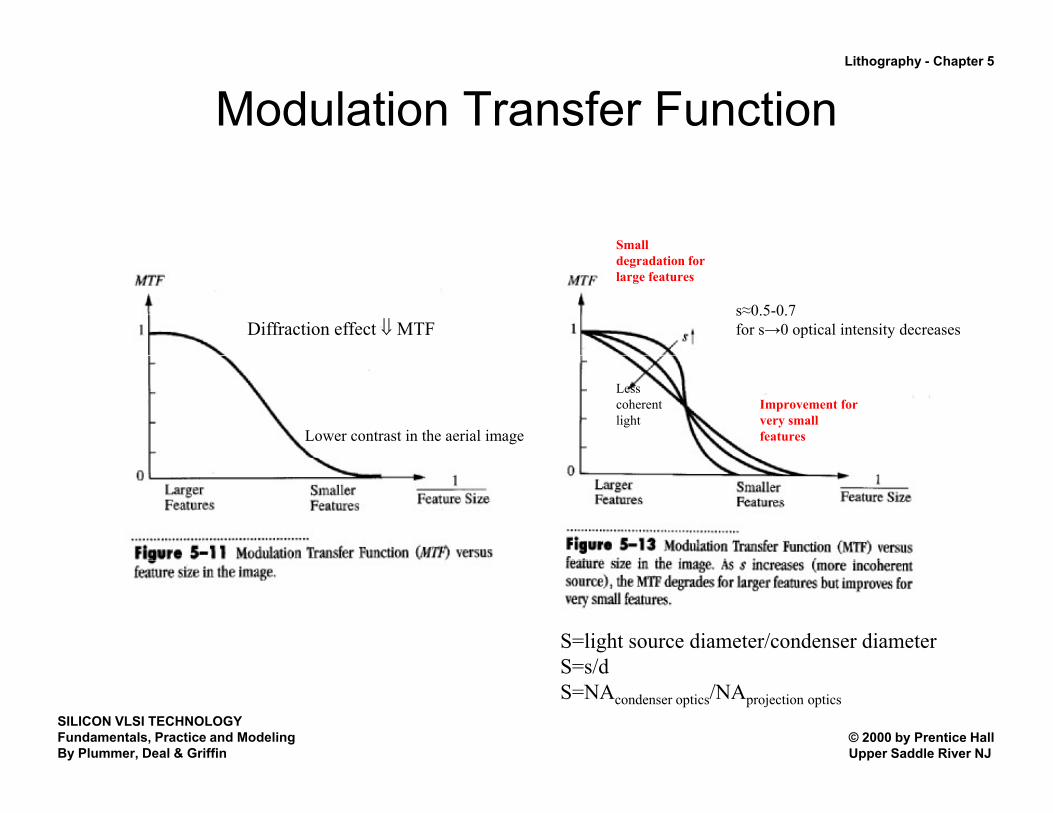
Modulation Transfer Function
Small
Diffraction effect ⇓ MTFs≈0.5-0.7 for s→0 optical intensity decreases
degradation for large features
Lower contrast in the aerial image
Less coherent light
Improvement for very small features
S=light source diameter/condenser diameterS /d
SILICON VLSI TECHNOLOGYFundamentals, Practice and ModelingBy Plummer, Deal & Griffin
© 2000 by Prentice HallUpper Saddle River NJ
S=s/dS=NAcondenser optics/NAprojection optics
Lithography - Chapter 5
Photoresist• Designed to respond to incident photons by changing
their properties when exposed to light.– Long-lived response require a chemical change
• Most resists are hydrocarbon-based materials.Photons break chemical nonds– Photons break chemical nonds
• Positive resists become more soluble in the developer solution– Typically used and have better resolution
N ti i t d th it• Negative resists do the opposite.
• Spin coating typically employed
SILICON VLSI TECHNOLOGYFundamentals, Practice and ModelingBy Plummer, Deal & Griffin
© 2000 by Prentice HallUpper Saddle River NJ
• Spin coating typically employed
16
Lithography - Chapter 5
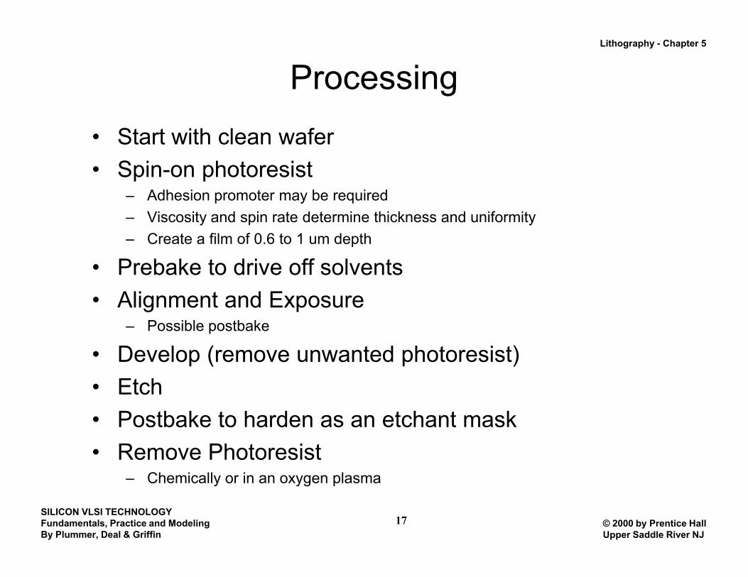
Processing• Start with clean wafer• Spin-on photoresistp p
– Adhesion promoter may be required– Viscosity and spin rate determine thickness and uniformity– Create a film of 0.6 to 1 um depth
• Prebake to drive off solvents• Alignment and Exposure
Possible postbake– Possible postbake
• Develop (remove unwanted photoresist)• Etch• Postbake to harden as an etchant mask• Remove Photoresist
SILICON VLSI TECHNOLOGYFundamentals, Practice and ModelingBy Plummer, Deal & Griffin
© 2000 by Prentice HallUpper Saddle River NJ
– Chemically or in an oxygen plasma
17
Lithography - Chapter 5
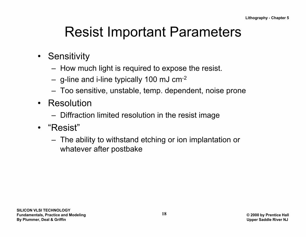
Resist Important Parameters• Sensitivity
– How much light is required to expose the resist.– g-line and i-line typically 100 mJ cm-2
– Too sensitive, unstable, temp. dependent, noise prone
• Resolution• Resolution– Diffraction limited resolution in the resist image
• “Resist”– The ability to withstand etching or ion implantation or
whatever after postbake
SILICON VLSI TECHNOLOGYFundamentals, Practice and ModelingBy Plummer, Deal & Griffin
© 2000 by Prentice HallUpper Saddle River NJ
18
Lithography - Chapter 5
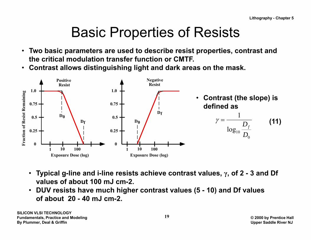
Basic Properties of Resists• Two basic parameters are used to describe resist properties, contrast and
the critical modulation transfer function or CMTF. • Contrast allows distinguishing light and dark areas on the mask.
mai
ning
0.75
1.0
0.75
1.0
Positive Resist
Negative Resist
• Contrast (the slope) is defined as
ion
of R
esis
t Rem
0.25
0.5
0.75
0.25
0.5
0.75
D0Df D0
Dfdefined as
10log
1
DDf
=γ (11)
Frac
ti
0
Exposure Dose (log)1 10 100
Exposure Dose (log)1 10 100
00D
• Typical g-line and i-line resists achieve contrast values, γ, of 2 - 3 and Df values of about 100 mJ cm-2.
• DUV resists have much higher contrast values (5 - 10) and Df values
SILICON VLSI TECHNOLOGYFundamentals, Practice and ModelingBy Plummer, Deal & Griffin
© 2000 by Prentice HallUpper Saddle River NJ
19
of about 20 - 40 mJ cm-2.
Lithography - Chapter 5
Critical MTF1.0
0.5
0.75
1.0
xpos
ure
Dos
eDf
Areal Image
0.25
0
Ex
Position
D0
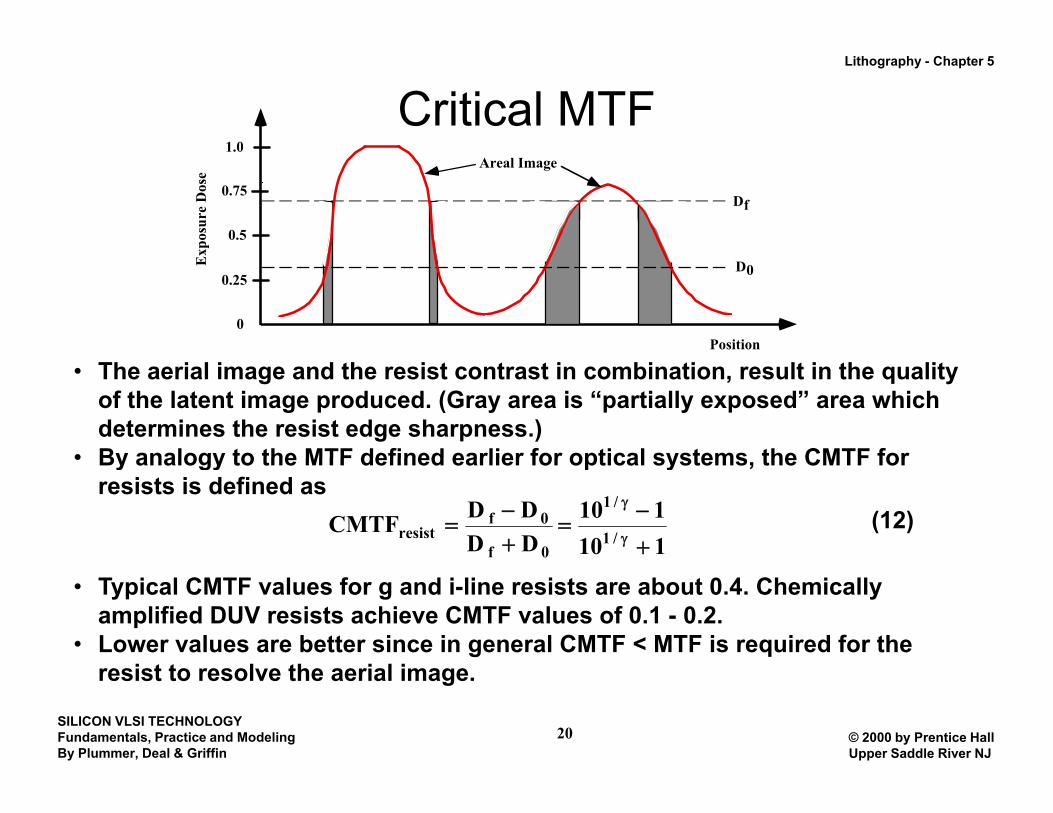
• The aerial image and the resist contrast in combination, result in the quality of the latent image produced. (Gray area is “partially exposed” area which determines the resist edge sharpness.)
• By analogy to the MTF defined earlier for optical systems the CMTF for• By analogy to the MTF defined earlier for optical systems, the CMTF for resists is defined as
CMTFresist = D f − D 0
D f + D 0= 101 / γ − 1
101 / γ + 1(12)
• Typical CMTF values for g and i-line resists are about 0.4. Chemically amplified DUV resists achieve CMTF values of 0.1 - 0.2.
• Lower values are better since in general CMTF < MTF is required for the
SILICON VLSI TECHNOLOGYFundamentals, Practice and ModelingBy Plummer, Deal & Griffin
© 2000 by Prentice HallUpper Saddle River NJ
20
resist to resolve the aerial image.
Lithography - Chapter 5
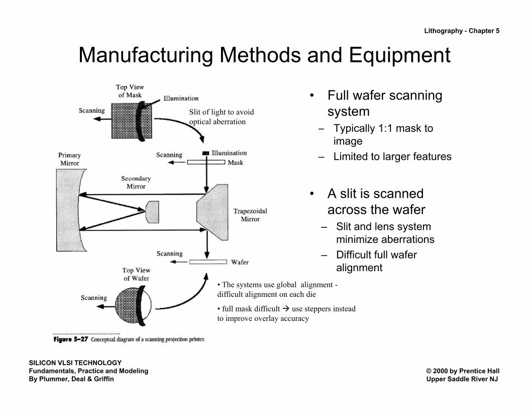
Manufacturing Methods and Equipment
Slit of light to avoid optical aberration
• Full wafer scanning system
Typically 1:1 mask to– Typically 1:1 mask to image
– Limited to larger features
• A slit is scanned across the wafer
– Slit and lens system
Th l b l li
yminimize aberrations
– Difficult full wafer alignment
• The systems use global alignment -difficult alignment on each die
• full mask difficult use steppers instead to improve overlay accuracy
SILICON VLSI TECHNOLOGYFundamentals, Practice and ModelingBy Plummer, Deal & Griffin
© 2000 by Prentice HallUpper Saddle River NJ

Lithography - Chapter 5
Manufacturing Methods and EquipmentCombined stepper + scanner 4X-5X larger mask pattern- difference in scanning speeds.• Stepper System
– 4x to 5x mask– Step, align, scan-slit
SILICON VLSI TECHNOLOGYFundamentals, Practice and ModelingBy Plummer, Deal & Griffin
© 2000 by Prentice HallUpper Saddle River NJ
Lithography - Chapter 5
Measurements of Masks• Check Masks for Features and Defects
– Scan– Make a new mask or Correct the errors
Corrections = repairs made by lasers (evaporation of Cr=excess by focusing)
Defects of sizes below critical dimensions will not print on PR
SILICON VLSI TECHNOLOGYFundamentals, Practice and ModelingBy Plummer, Deal & Griffin
© 2000 by Prentice HallUpper Saddle River NJ
Lithography - Chapter 5
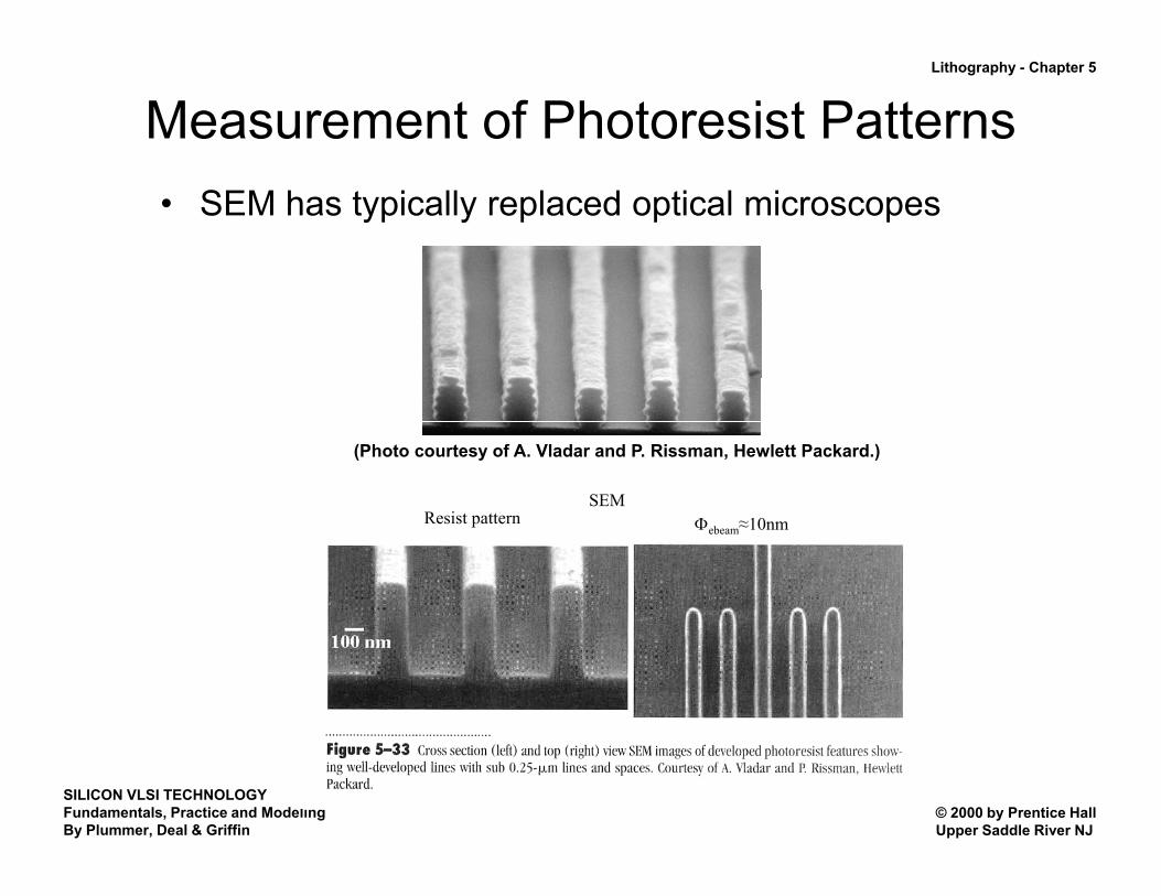
Measurement of Photoresist Patterns• SEM has typically replaced optical microscopes
SEM
(Photo courtesy of A. Vladar and P. Rissman, Hewlett Packard.)
SEMResist pattern Φebeam≈10nm
SILICON VLSI TECHNOLOGYFundamentals, Practice and ModelingBy Plummer, Deal & Griffin
© 2000 by Prentice HallUpper Saddle River NJ
Lithography - Chapter 5
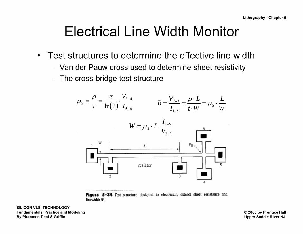
Electrical Line Width Monitor• Test structures to determine the effective line width
– Van der Pauw cross used to determine sheet resistivity– The cross-bridge test structure
( )43−⋅==
VS
πρρ LLVR ⋅− ρρ32( ) 652ln −ItSρ
WWtIR S ⋅=
⋅==
−
ρ51
32
51−⋅⋅=VILW Sρ
32−V
resistor
SILICON VLSI TECHNOLOGYFundamentals, Practice and ModelingBy Plummer, Deal & Griffin
© 2000 by Prentice HallUpper Saddle River NJ
Lithography - Chapter 5
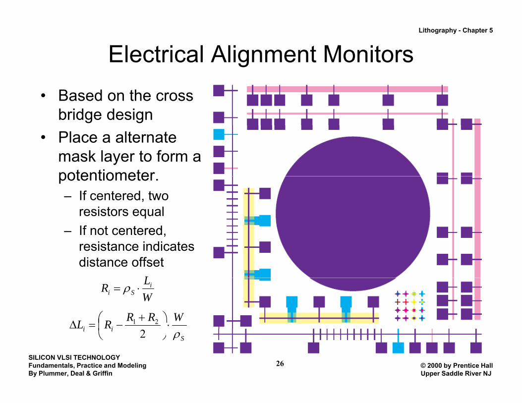
Electrical Alignment Monitors• Based on the cross
bridge design• Place a alternate
mask layer to form a potentiometerpotentiometer.– If centered, two
resistors equalIf t t d– If not centered, resistance indicates distance offset
LWLR i
Si ⋅= ρ
iiWRRRL ⋅⎟
⎠⎞
⎜⎝⎛ +
−=Δ 21
SILICON VLSI TECHNOLOGYFundamentals, Practice and ModelingBy Plummer, Deal & Griffin
© 2000 by Prentice HallUpper Saddle River NJ
26
Sii ρ
⎟⎠
⎜⎝ 2
Lithography - Chapter 5
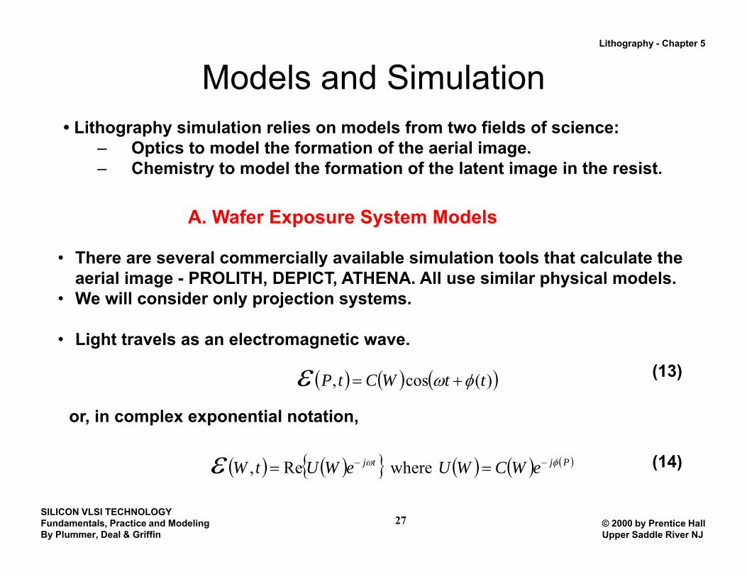
Models and Simulation• Lithography simulation relies on models from two fields of science:
– Optics to model the formation of the aerial image.– Chemistry to model the formation of the latent image in the resist.
A. Wafer Exposure System Models
Th l i ll il bl i l ti t l th t l l t th• There are several commercially available simulation tools that calculate the aerial image - PROLITH, DEPICT, ATHENA. All use similar physical models.
• We will consider only projection systems.
• Light travels as an electromagnetic wave.
( ) ( ) ( ))(cos, ttWCtP φωε += (13)
( ) ( ){ } ( ) ( ) ( )Pjtj eWCWUeWUtW φωε −− == whereRe
or, in complex exponential notation,
(14)
SILICON VLSI TECHNOLOGYFundamentals, Practice and ModelingBy Plummer, Deal & Griffin
© 2000 by Prentice HallUpper Saddle River NJ
27
( ) ( ){ } ( ) ( )eWCWUeWUtWε == whereRe, ( )
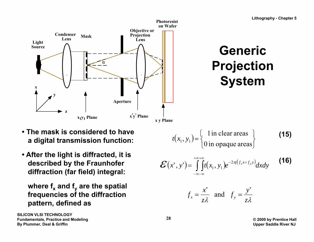
Lithography - Chapter 5
Light
Condenser Lens
Objective orProjection Lens
Photoresist on Wafer
Mask
Generic Projection
Source
α
SystemAperture
x
y
zx1y1 Plane x'y' Plane
x y Plane
• The mask is considered to have ( ) ⎬
⎫⎨⎧ areasclear in 1 (15)
a digital transmission function:
• After the light is diffracted, it is described by the Fraunhofer
( )⎭⎬⎫
⎩⎨⎧
=areas opaquein 0
, 11 yxt (15)
( ) ( ) ( )∫ ∫+∞+∞
+−= dxdyeyxtyx yfxfj yxπε 211,’,’
(16)ydiffraction (far field) integral:
where fx and fy are the spatial frequencies of the diffraction
( ) ( )∫ ∫∞− ∞−
dxdyeyxtyxε 11,,
λλyfxf yx’ and ’
==
SILICON VLSI TECHNOLOGYFundamentals, Practice and ModelingBy Plummer, Deal & Griffin
© 2000 by Prentice HallUpper Saddle River NJ
28
qpattern, defined as λλ z
fz
f yx
Lithography - Chapter 5
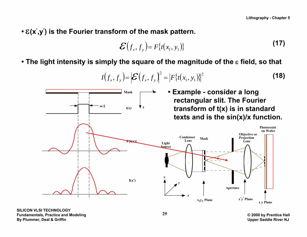
• ε(x’,y’) is the Fourier transform of the mask pattern.
( ) ( ){ }ε (17)( ) ( ){ }11,, yxtFff yx =ε (17)
• The light intensity is simply the square of the magnitude of the ε field, so that
( ) ( ) ( ){ }22ε (18)( ) ( ) ( ){ }211
2,,, yxtFffffI yxyx == ε (18)
• Example - consider a long rectangular slit. The Fourier
Mask x
gtransform of t(x) is in standard texts and is the sin(x)/x function.
t(x)w/2 z
Obj ti
Photoresist on Wafer
F{t(x)} LightSource
Condenser Lens
Objective orProjection Lens
Mask
α
I(x')
Aperture
x
y
SILICON VLSI TECHNOLOGYFundamentals, Practice and ModelingBy Plummer, Deal & Griffin
© 2000 by Prentice HallUpper Saddle River NJ
29
zx1y1 Plane x'y' Plane
x y Plane
Lithography - Chapter 5
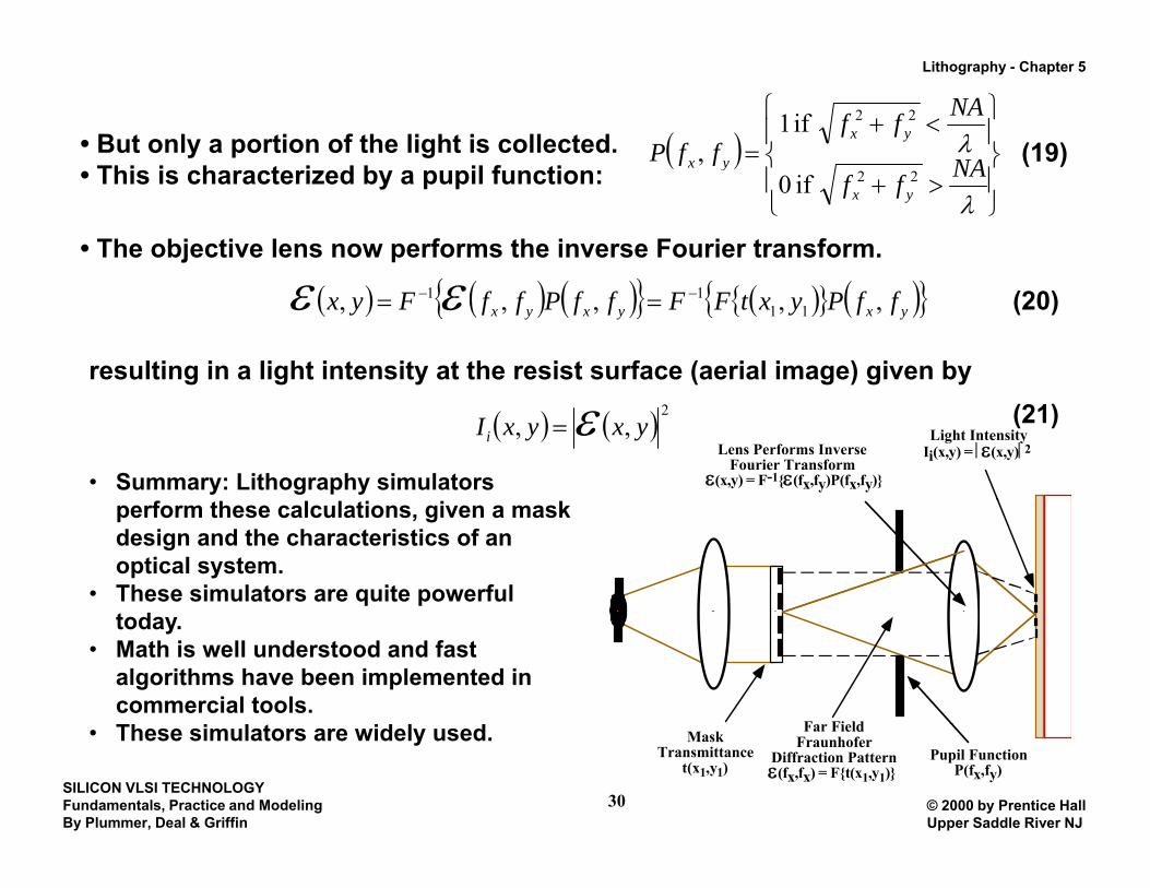
• But only a portion of the light is collected. ( ) ⎪⎬
⎫⎪⎨
⎧ <+= λ
NA
NAffffP
yx
yx
22 if 1, (19)
• This is characterized by a pupil function:( )
⎪⎭
⎬⎪⎩
⎨>+
λNAff
ffyx
yx22 if 0
, ( )
• The objective lens now performs the inverse Fourier transform.
( ) ( ) ( ){ } ( ){ } ( ){ }yxyxyx ffPyxtFFffPffFyx ,,,,, 1111 −− == εε (20)
resulting in a light intensity at the resist surface (aerial image) given by
( ) ( ) 2,, yxyxIi ε= (21)
• Summary: Lithography simulators Lens Performs Inverse
Fourier Transform
Light Intensity
ε(x,y) = F-1{ε(fx,fy)P(fx,fy)}
Ii(x,y) = ⎥ε(x,y)⎥2
perform these calculations, given a mask design and the characteristics of an optical system.
• These simulators are quite powerful today.
• Math is well understood and fast algorithms have been implemented in commercial tools. Th i l id l d Far Field
SILICON VLSI TECHNOLOGYFundamentals, Practice and ModelingBy Plummer, Deal & Griffin
© 2000 by Prentice HallUpper Saddle River NJ
30
• These simulators are widely used. MaskTransmittance
t(x1,y1)
Far FieldFraunhofer
Diffraction Pattern Pupil FunctionP(fx,fy)ε(fx,fx) = F{t(x1,y1)}
Lithography - Chapter 5
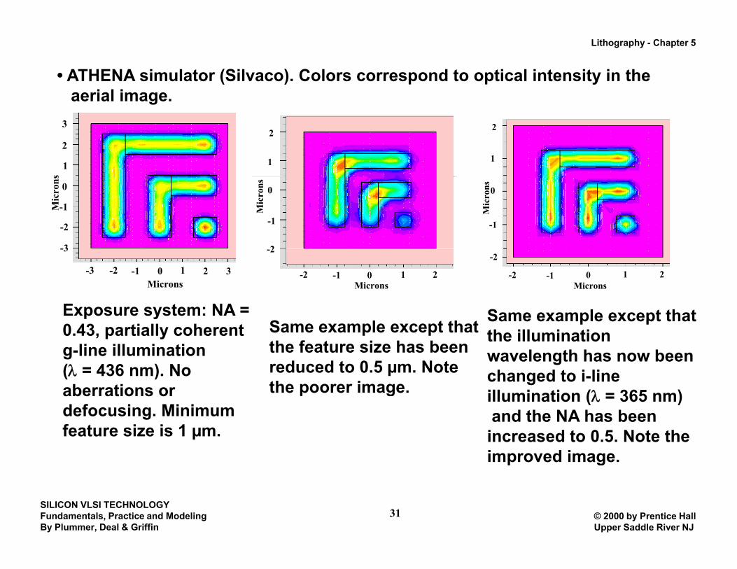
• ATHENA simulator (Silvaco). Colors correspond to optical intensity in the aerial image.
s
1
2
3
1
2
1
2
Mic
rons 0
-1
-2
-3M
icro
ns 0
-1
2
Mic
rons 0
-1
Microns-3 0 1 2 3-1-2
-3
Microns0 1 2-1-2
-2-2
Microns0 1 2-1-2
Exposure system: NA = S l h Same example except that
0.43, partially coherent g-line illumination (λ = 436 nm). No aberrations or
Same example except that the feature size has been reduced to 0.5 µm. Note the poorer image.
Same example except that the illumination wavelength has now been changed to i-line ill i ti (λ 365 )aberrations or
defocusing. Minimum feature size is 1 µm.
the poorer image. illumination (λ = 365 nm)and the NA has been increased to 0.5. Note the improved image.
SILICON VLSI TECHNOLOGYFundamentals, Practice and ModelingBy Plummer, Deal & Griffin
© 2000 by Prentice HallUpper Saddle River NJ
31
p g
Lithography - Chapter 5
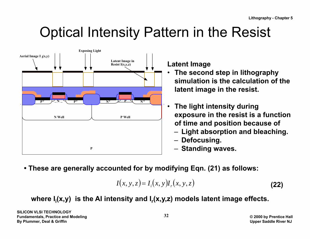
Optical Intensity Pattern in the ResistAerial Image I i(x,y)
Exposing Light
Latent Image inResist I(x,y,z) Latent Image
• The second step in lithography
PNP+ P+ N+ N+
The second step in lithography simulation is the calculation of the latent image in the resist.
Th li ht i t it d iP WellN Well
• The light intensity during exposure in the resist is a function of time and position because of– Light absorption and bleaching.
P
g p g– Defocusing.– Standing waves.
• These are generally accounted for by modifying Eqn. (21) as follows:
( ) ( ) ( )zyxIyxIzyxI ri ,,,,, = (22)
SILICON VLSI TECHNOLOGYFundamentals, Practice and ModelingBy Plummer, Deal & Griffin
© 2000 by Prentice HallUpper Saddle River NJ
32
where Ii(x,y) is the AI intensity and Ir(x,y,z) models latent image effects.
Lithography - Chapter 5
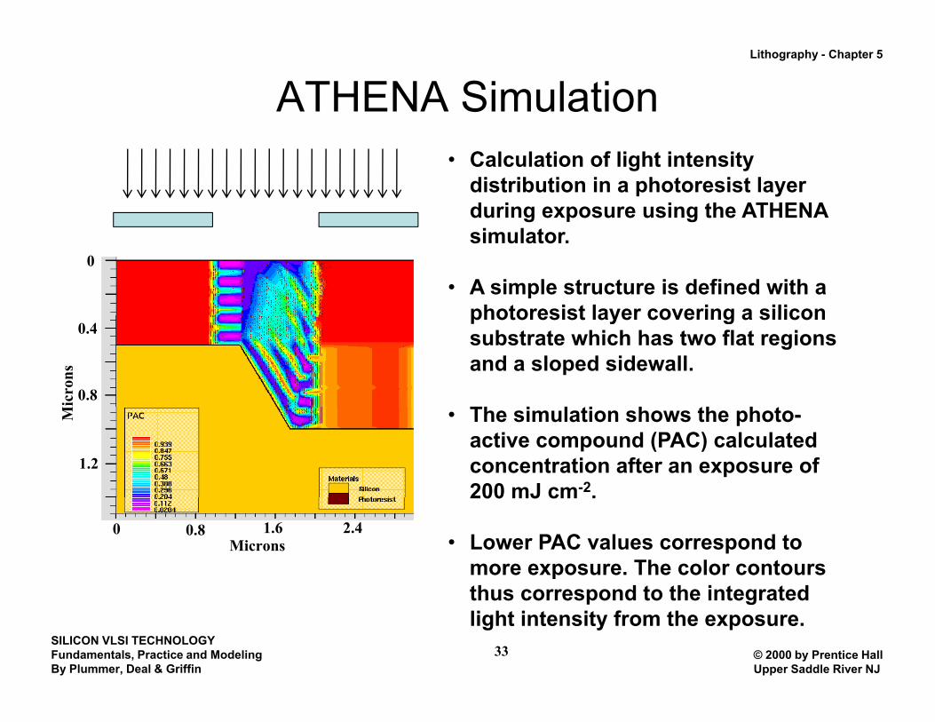
ATHENA Simulation• Calculation of light intensity
distribution in a photoresist layer during exposure using the ATHENA
0simulator.
• A simple structure is defined with a photoresist layer covering a silicon
Mic
rons
0.4
0.8
photoresist layer covering a silicon substrate which has two flat regions and a sloped sidewall.
Th i l i h h hM
1.2
• The simulation shows the photo-active compound (PAC) calculated concentration after an exposure of 200 mJ cm-2.
Microns0 0.8 1.6 2.4
200 mJ cm .
• Lower PAC values correspond to more exposure. The color contours th d t th i t t d
SILICON VLSI TECHNOLOGYFundamentals, Practice and ModelingBy Plummer, Deal & Griffin
© 2000 by Prentice HallUpper Saddle River NJ
33
thus correspond to the integrated light intensity from the exposure.
Lithography - Chapter 5
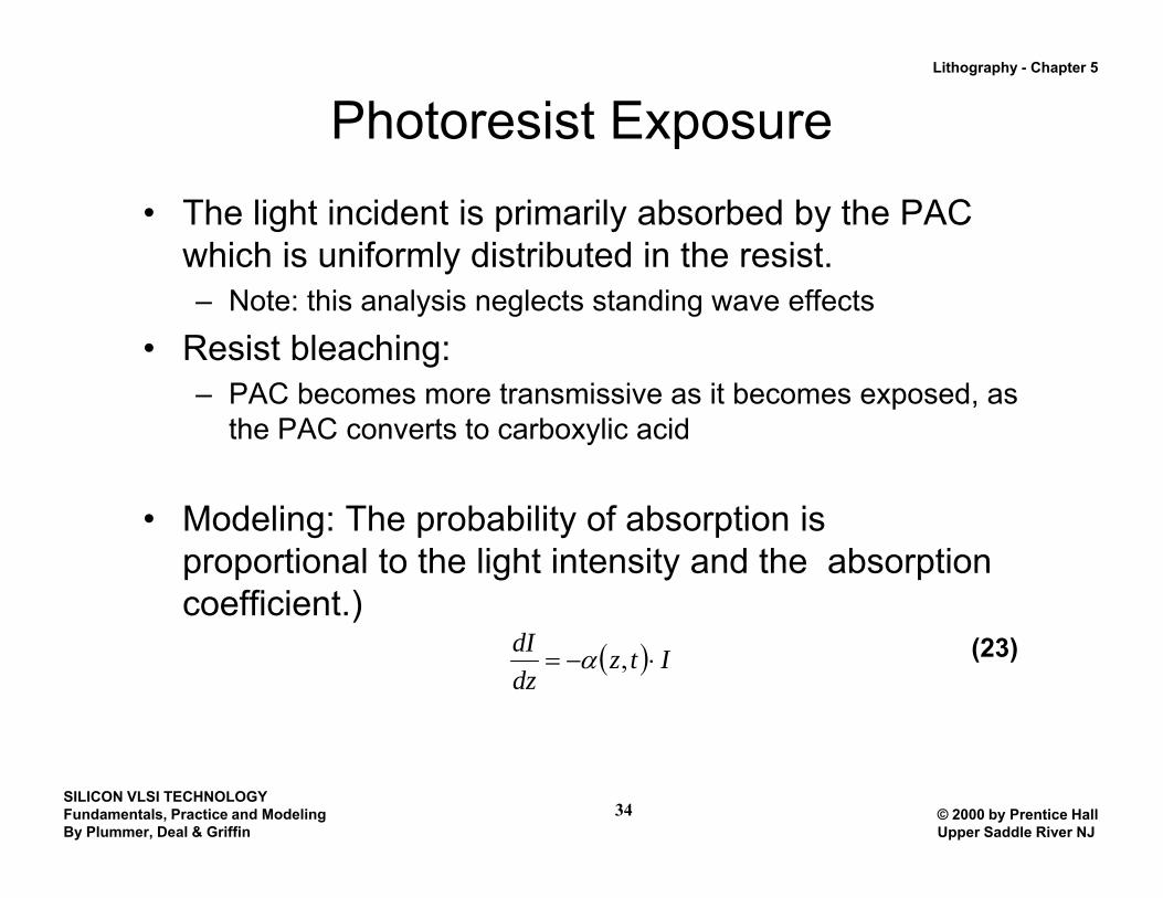
Photoresist Exposure• The light incident is primarily absorbed by the PAC
which is uniformly distributed in the resist.– Note: this analysis neglects standing wave effects
• Resist bleaching:PAC becomes more transmissive as it becomes exposed as– PAC becomes more transmissive as it becomes exposed, as the PAC converts to carboxylic acid
M d li Th b bili f b i i• Modeling: The probability of absorption is proportional to the light intensity and the absorption coefficient.))
( ) ItzdzdI
⋅−= ,α (23)
SILICON VLSI TECHNOLOGYFundamentals, Practice and ModelingBy Plummer, Deal & Griffin
© 2000 by Prentice HallUpper Saddle River NJ
34
Lithography - Chapter 5
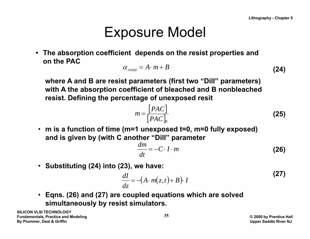
Exposure Model• The absorption coefficient depends on the resist properties and
on the PACBmAresist +⋅=α (24)
where A and B are resist parameters (first two “Dill” parameters) with A the absorption coefficient of bleached and B nonbleachedresist. Defining the percentage of unexposed resit
[ ][ ]0PACPACm = (25)
• m is a function of time (m=1 unexposed t=0, m=0 fully exposed) and is given by (with C another “Dill” parameter
mICdtdm
⋅⋅−= (26)
Substituting (24) into (23) we have:• Substituting (24) into (23), we have:
( )( ) IBtzmAdzdI
⋅+⋅−= ,(27)
• Eqns (26) and (27) are coupled equations which are solved
SILICON VLSI TECHNOLOGYFundamentals, Practice and ModelingBy Plummer, Deal & Griffin
© 2000 by Prentice HallUpper Saddle River NJ
35
• Eqns. (26) and (27) are coupled equations which are solved simultaneously by resist simulators.
Lithography - Chapter 5
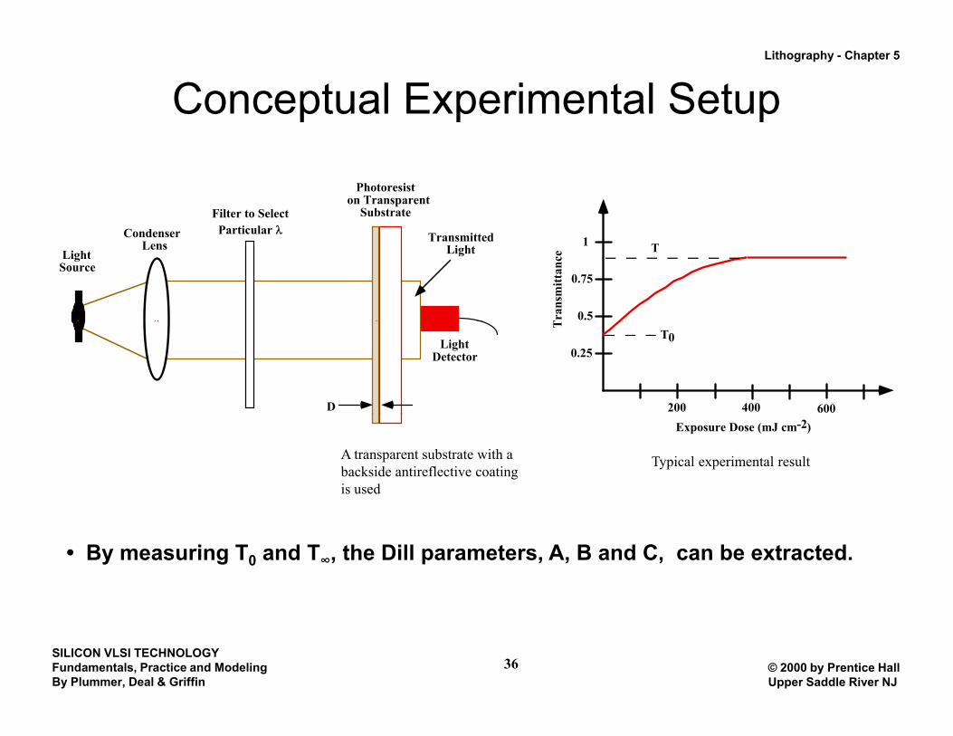
Conceptual Experimental Setup
C d
Photoresist on Transparent
SubstrateFilter to SelectParticular λ
LightSource
Condenser Lens
Particular λ TransmittedLight
Tra
nsm
ittan
ce
1
0.75
0.5
T�
LightDetector
D
T
0.25
200 400 600
T0
Exposure Dose (mJ cm-2)
A transparent substrate with a backside antireflective coating is used
Typical experimental result
• By measuring T0 and T∞, the Dill parameters, A, B and C, can be extracted.
SILICON VLSI TECHNOLOGYFundamentals, Practice and ModelingBy Plummer, Deal & Griffin
© 2000 by Prentice HallUpper Saddle River NJ
36
Lithography - Chapter 5
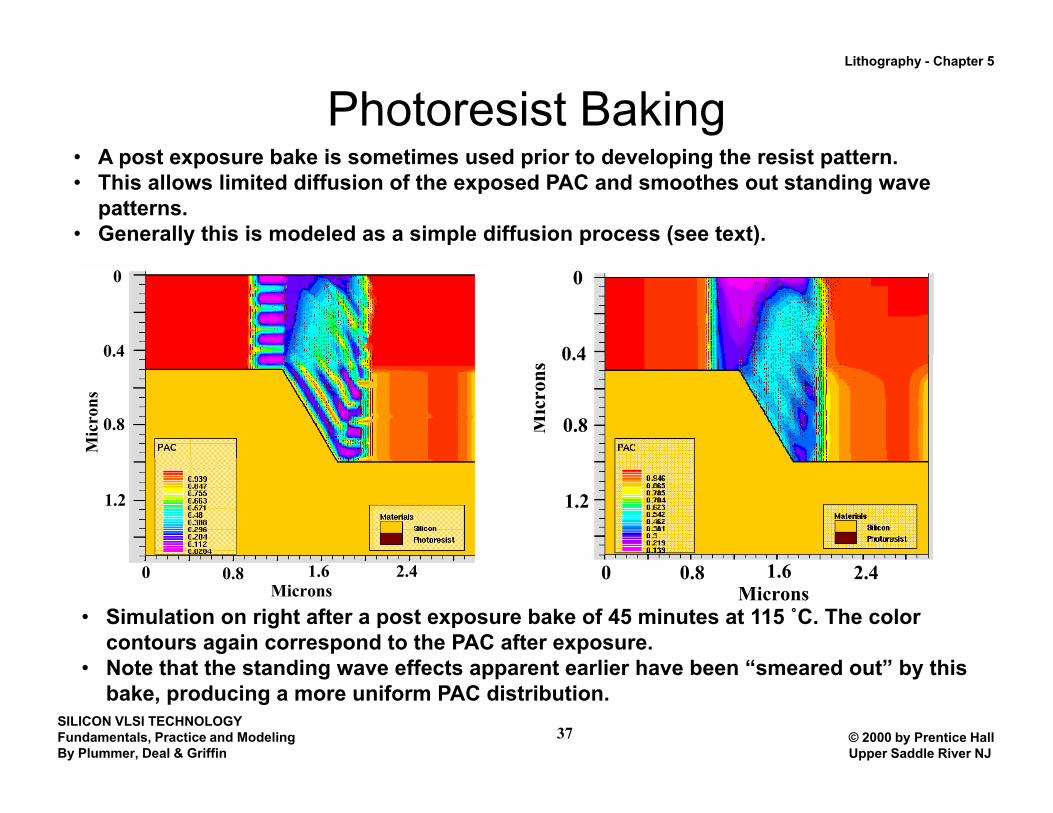
Photoresist BakingA t b k i ti d i t d l i th i t tt• A post exposure bake is sometimes used prior to developing the resist pattern.
• This allows limited diffusion of the exposed PAC and smoothes out standing wave patterns.
• Generally this is modeled as a simple diffusion process (see text).
0
0 4
0
0.4
Mic
rons
0.4
0.8
Mic
rons
0.4
0.8
1.21.2
Microns0.8 1.6 2.40
Microns0 0.8 1.6 2.4
• Simulation on right after a post exposure bake of 45 minutes at 115 ˚C. The color contours again correspond to the PAC after exposure. N t th t th t di ff t t li h b “ d t” b thi
SILICON VLSI TECHNOLOGYFundamentals, Practice and ModelingBy Plummer, Deal & Griffin
© 2000 by Prentice HallUpper Saddle River NJ
37
• Note that the standing wave effects apparent earlier have been “smeared out” by this bake, producing a more uniform PAC distribution.
Lithography - Chapter 5
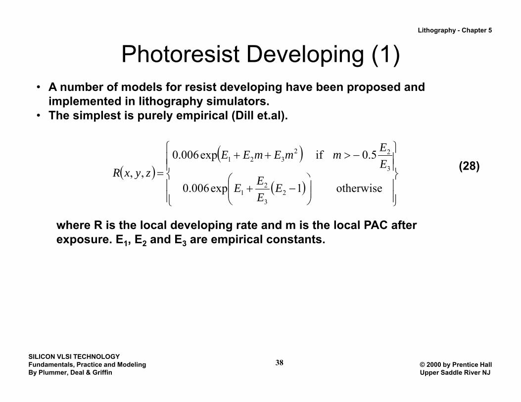
Photoresist Developing (1)• A number of models for resist developing have been proposed and
implemented in lithography simulators.• The simplest is purely empirical (Dill et.al).
( )( )
⎪⎪⎬
⎫⎪⎪⎨
⎧
⎞⎛
−>++=
5.0 if exp006.0,, 3
22321 E
EmmEmEEzyxR (28)( )
( )⎪⎪⎭
⎬
⎪⎪⎩
⎨⎟⎟⎠
⎞⎜⎜⎝
⎛−+ otherwise 1exp006.0
,,2
3
21 E
EEE
zyxR
where R is the local developing rate and m is the local PAC afterwhere R is the local developing rate and m is the local PAC after exposure. E1, E2 and E3 are empirical constants.
SILICON VLSI TECHNOLOGYFundamentals, Practice and ModelingBy Plummer, Deal & Griffin
© 2000 by Prentice HallUpper Saddle River NJ
38
Lithography - Chapter 5
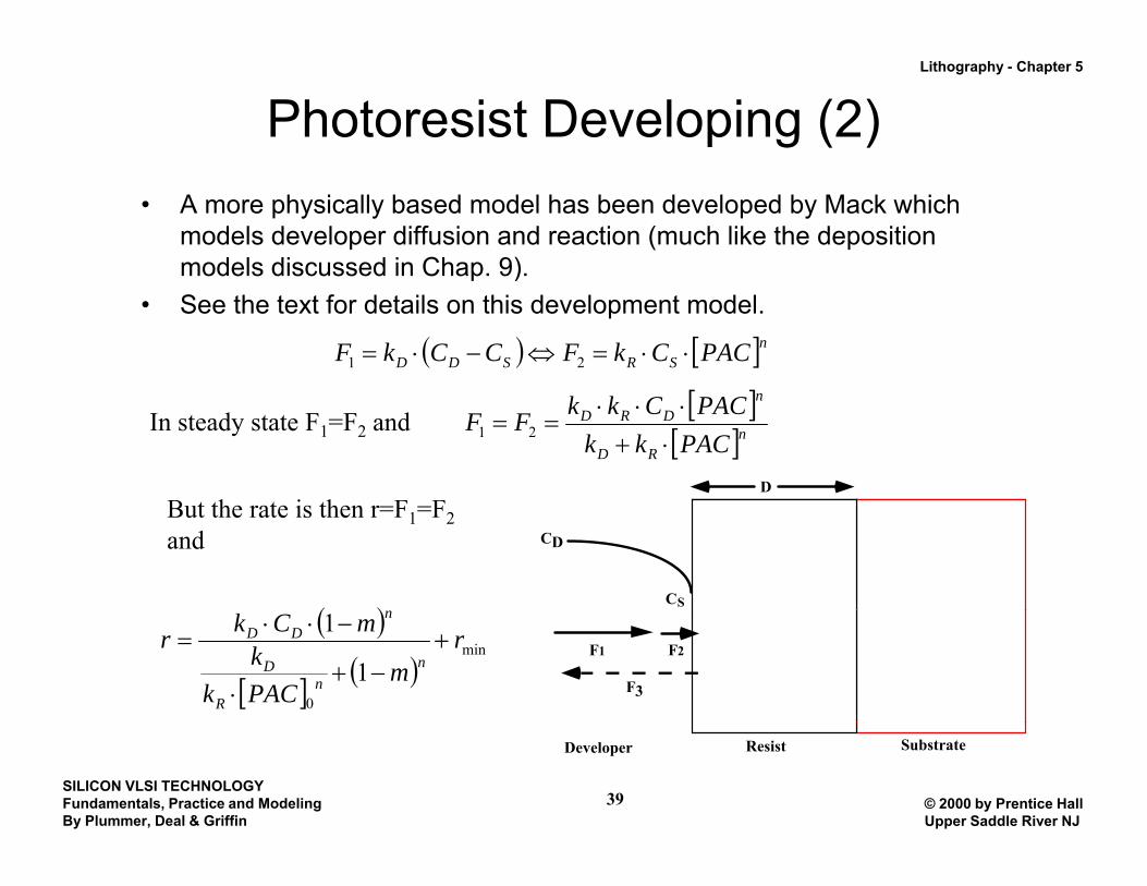
Photoresist Developing (2) • A more physically based model has been developed by Mack which
models developer diffusion and reaction (much like the deposition models discussed in Chap. 9).models discussed in Chap. 9).
• See the text for details on this development model.
( ) [ ]nSRSDD PACCkFCCkF ⋅⋅=⇔−⋅= 21
D
[ ][ ]n
RD
nDRD
PACkkPACCkkFF
⋅+⋅⋅⋅
== 21In steady state F1=F2 and
CS
CD
But the rate is then r=F1=F2and
( )F1 F2
F3
( )
[ ] ( )min
0
1
1 rm
PACkk
mCkrn
nR
D
nDD +
−+⋅
−⋅⋅=
SILICON VLSI TECHNOLOGYFundamentals, Practice and ModelingBy Plummer, Deal & Griffin
© 2000 by Prentice HallUpper Saddle River NJ
39
Resist SubstrateDeveloper
Lithography - Chapter 5
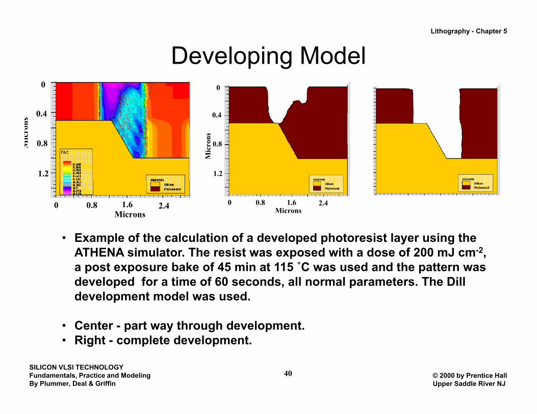
Developing Modelon
s
0
0.4
0
0.4
Mic
ro
0.8
1.2
Mic
rons
0.8
1.2
Microns0.8 1.6 2.40
Microns0.8 1.6 2.40
E l f h l l i f d l d h i l i h• Example of the calculation of a developed photoresist layer using the ATHENA simulator. The resist was exposed with a dose of 200 mJ cm-2, a post exposure bake of 45 min at 115 ˚C was used and the pattern was developed for a time of 60 seconds, all normal parameters. The Dilldeveloped for a time of 60 seconds, all normal parameters. The Dill development model was used.
• Center - part way through development. Ri ht l t d l t
SILICON VLSI TECHNOLOGYFundamentals, Practice and ModelingBy Plummer, Deal & Griffin
© 2000 by Prentice HallUpper Saddle River NJ
40
• Right - complete development.
Lithography - Chapter 5
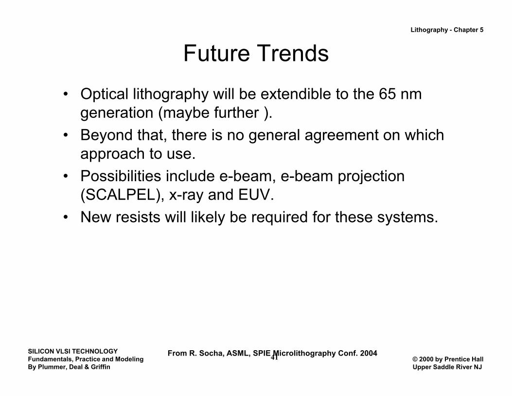
Future Trends• Optical lithography will be extendible to the 65 nm
generation (maybe further ).• Beyond that, there is no general agreement on which
approach to use.Possibilities include e beam e beam projection• Possibilities include e-beam, e-beam projection (SCALPEL), x-ray and EUV.
• New resists will likely be required for these systems.y q y
SILICON VLSI TECHNOLOGYFundamentals, Practice and ModelingBy Plummer, Deal & Griffin
© 2000 by Prentice HallUpper Saddle River NJ
41From R. Socha, ASML, SPIE Microlithography Conf. 2004
Lithography - Chapter 5
Techniques for Future Electronics• Lithography and Other Patterning Techniques for Future
ElectronicsBy R Fabian Pease Fellow IEEE and Stephen Y Chou Fellow IEEE– By R. Fabian Pease, Fellow IEEE, and Stephen Y. Chou, Fellow IEEE
– Proceedings of the IEEE, Vol. 96, No. 2, February 2008
• Projection OpticsProjection Optics– Light Sources: 248–193 nm (KrF and ArF excimer lasers)
• Immersion Optics: use a fluid instead of airExtreme Ultraviolet Lithography (EUVL)• Extreme Ultraviolet Lithography (EUVL)
• Resolution Enhancement Technology (RET)• Absorbance Modulation Optical Lithography (AMOL)• Electron and Ion Beam Lithography• X-ray Lithography• Nanoimprint Technology
SILICON VLSI TECHNOLOGYFundamentals, Practice and ModelingBy Plummer, Deal & Griffin
© 2000 by Prentice HallUpper Saddle River NJ
a o p t ec o ogy
42
Lithography - Chapter 5
Summary of Key Ideas• Lithography is the key pacing item for developing new technology
generations.• Exposure tools today generally use projection optics with diffraction• Exposure tools today generally use projection optics with diffraction
limited performance.• g and i-line resists based on DNQ materials and were used down to
0.35 µm.µ• DUV resists use chemical amplification and are generally used below
0.35 µm. • Lithography simulation tools are based on Fourier optics and do an
excellent job of simulating optical system performance. Thus aerial images can be accurately calculated.
• Photoresist modeling (exposure, development, postbake) is less advanced because chemistry is involved which is not as welladvanced because chemistry is involved which is not as well understood. Thus latent images are less accurately calculated today.
• A new approach to lithography may be required in the next 10 years.
SILICON VLSI TECHNOLOGYFundamentals, Practice and ModelingBy Plummer, Deal & Griffin
© 2000 by Prentice HallUpper Saddle River NJ
43


![Ece-V-fundamentals of Cmos Vlsi [10ec56]-Notes](https://img.pdfslide.us/doc/110x75/55cf98ff550346d0339aef5e/ece-v-fundamentals-of-cmos-vlsi-10ec56-notes-562652a532888.jpg)