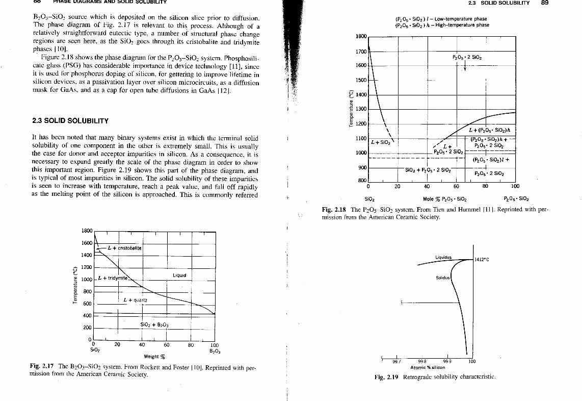
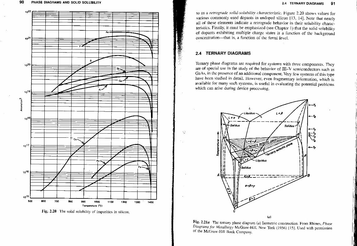
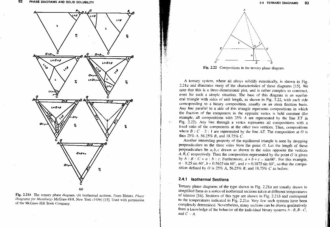
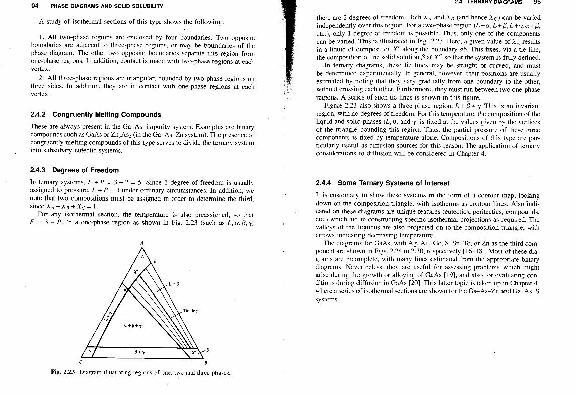
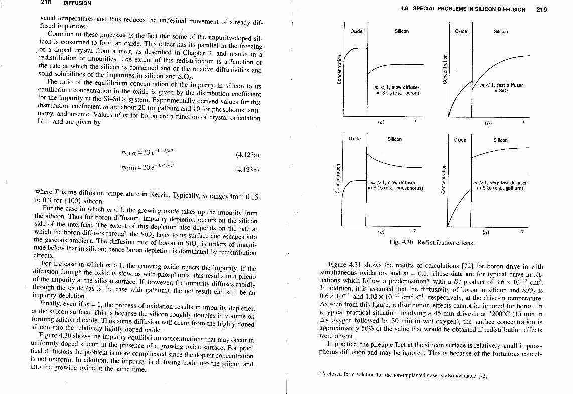
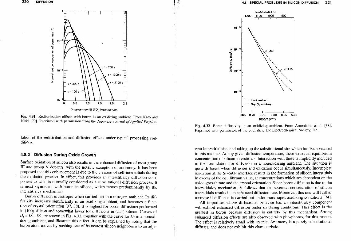
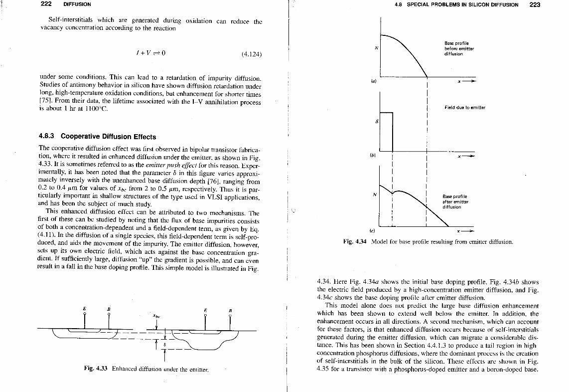
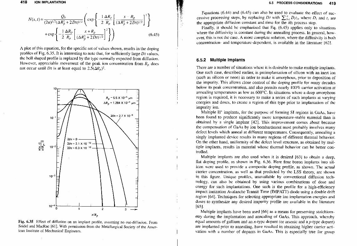
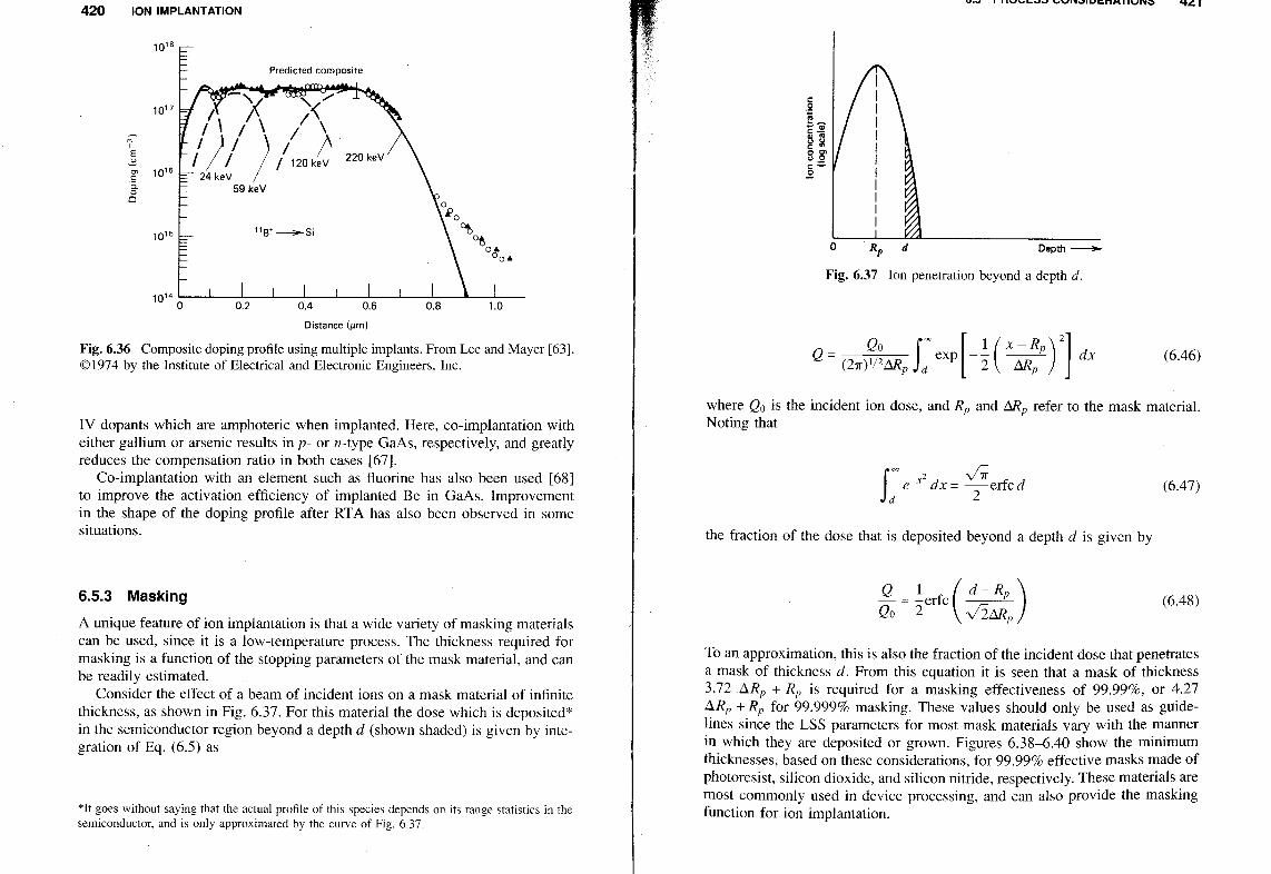
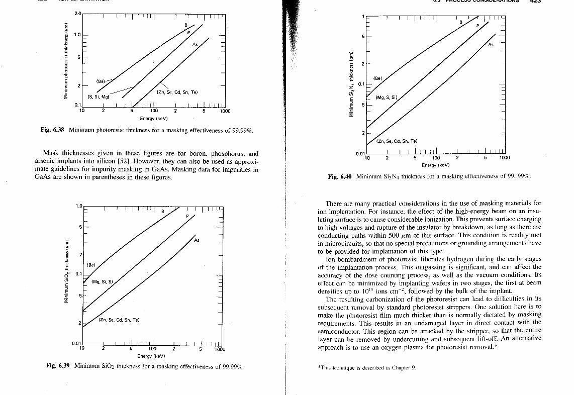
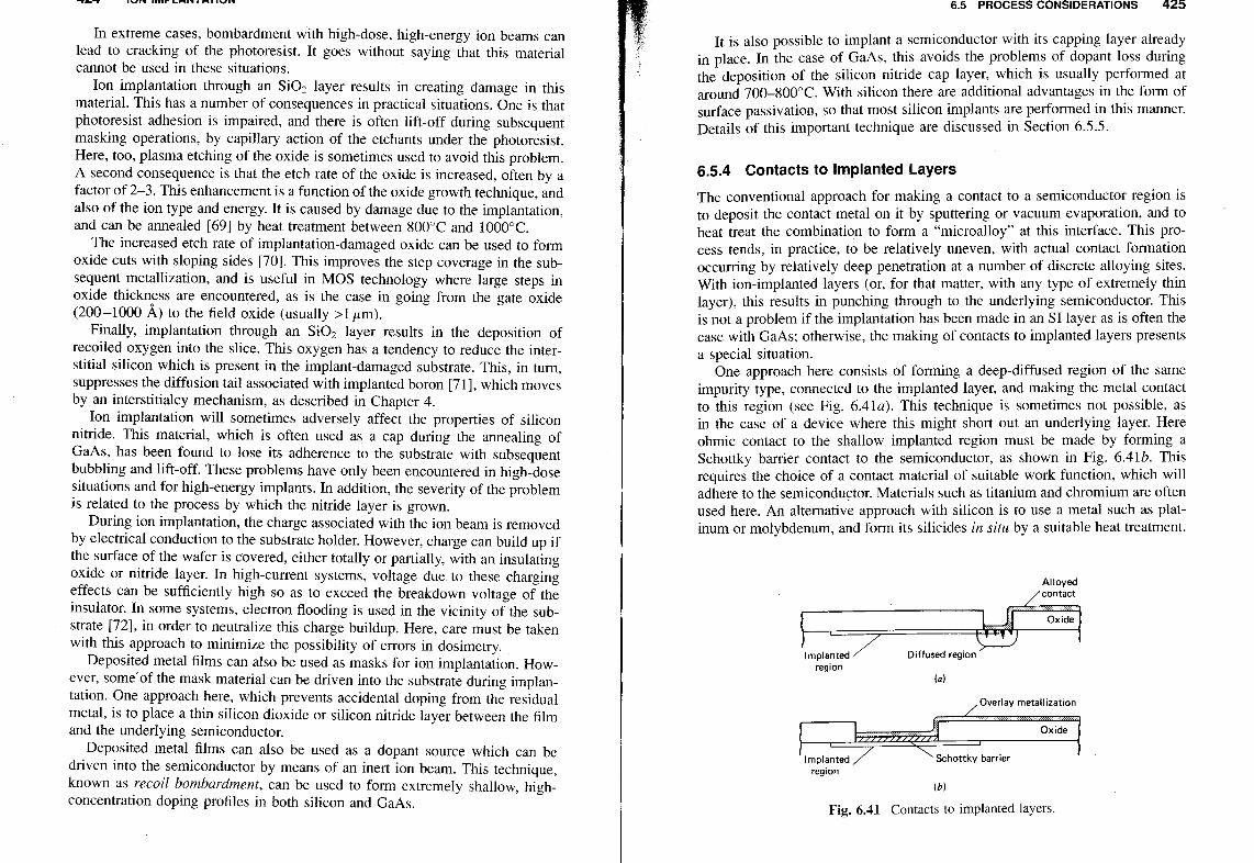
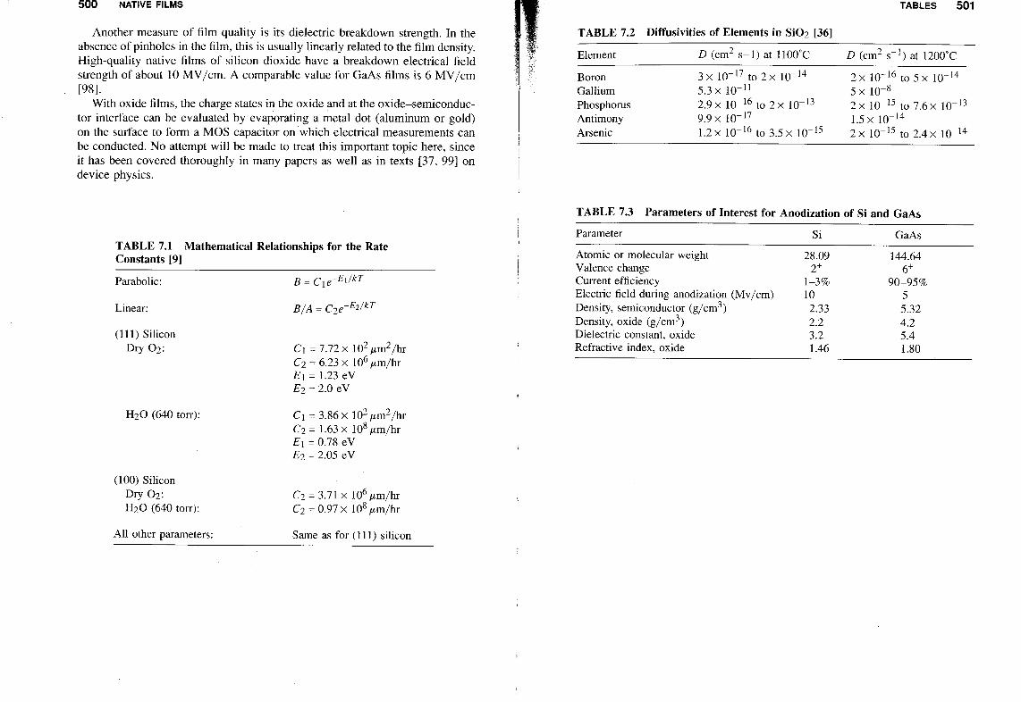
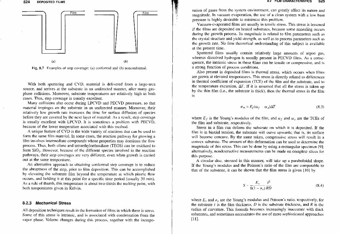
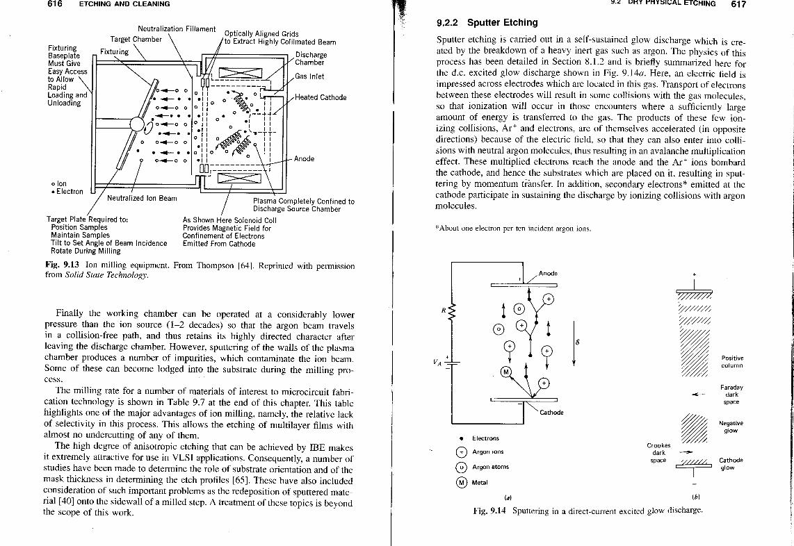
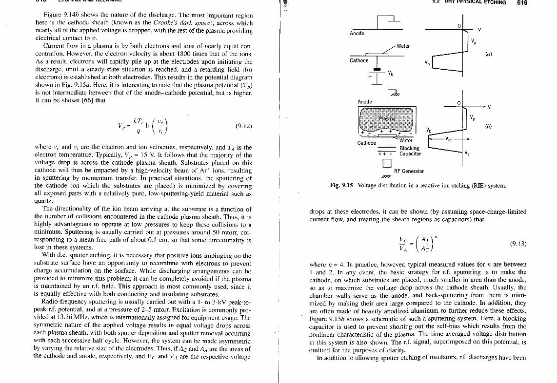
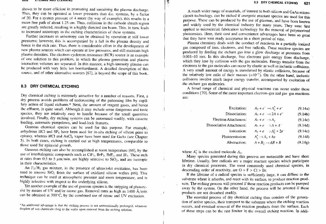
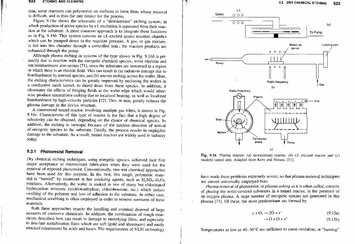
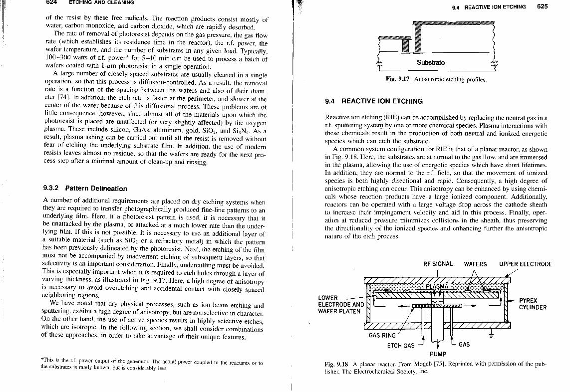
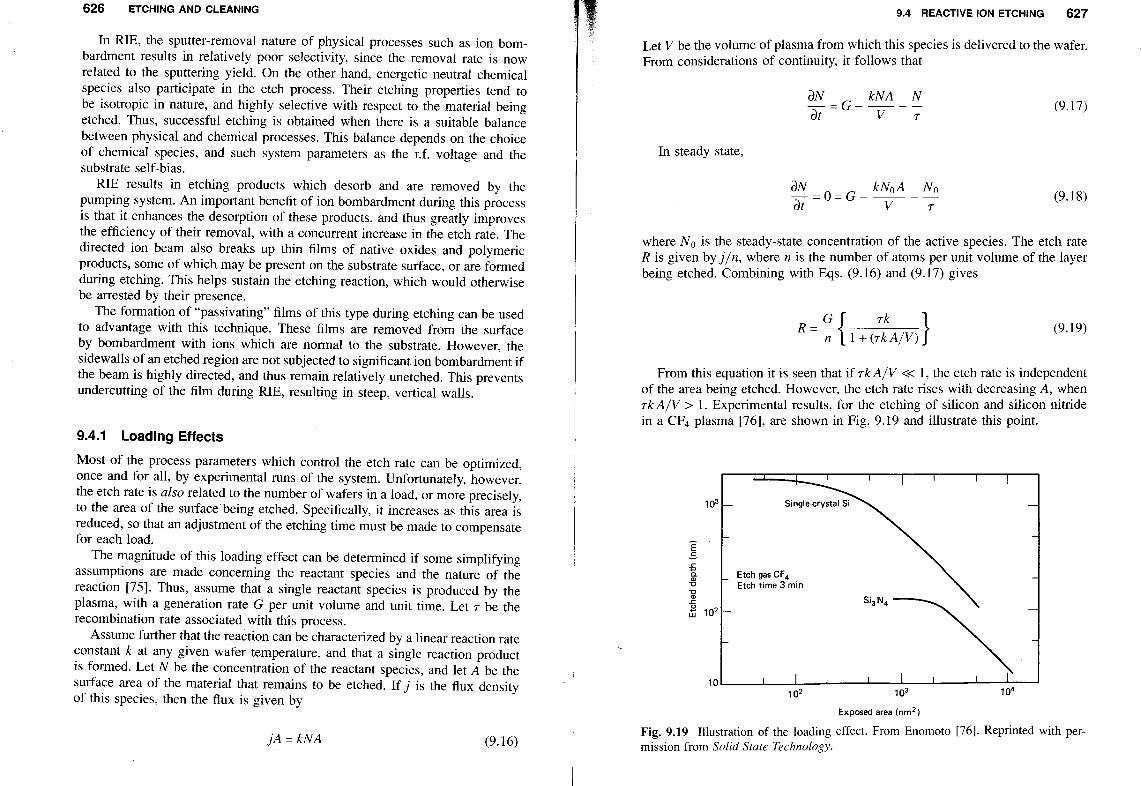
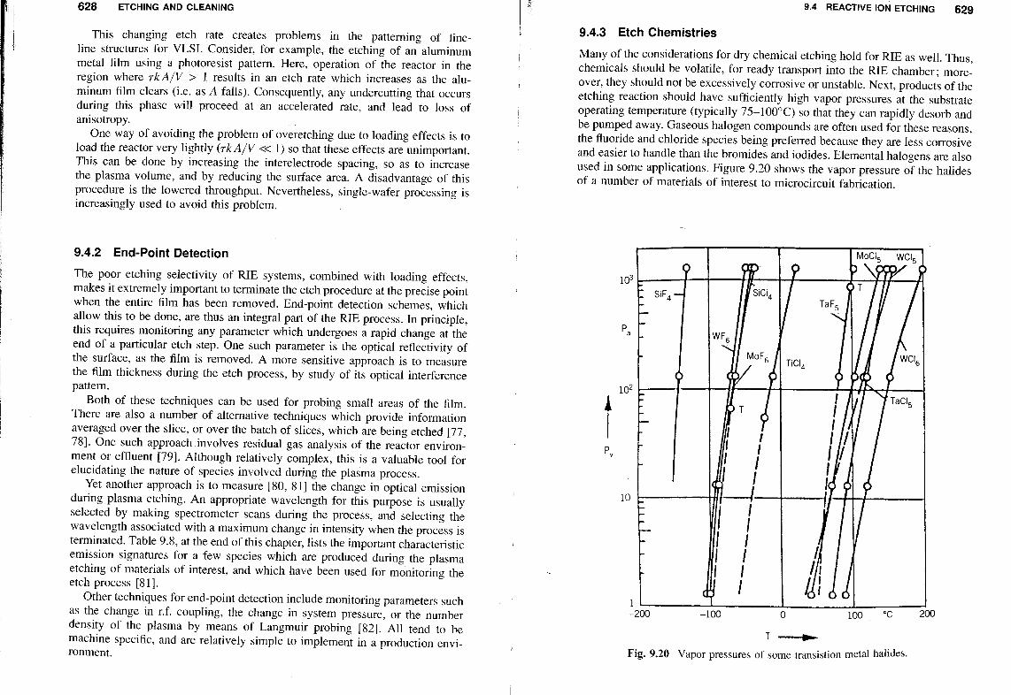
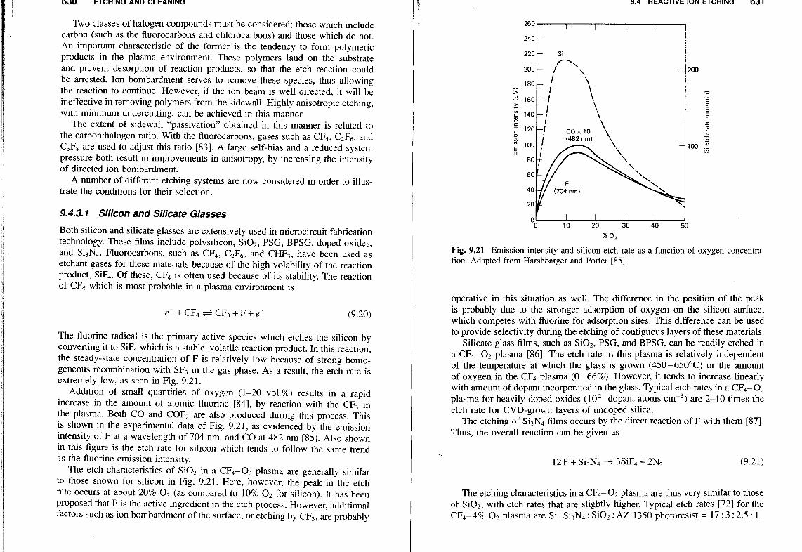
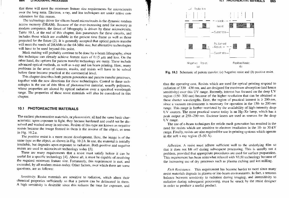
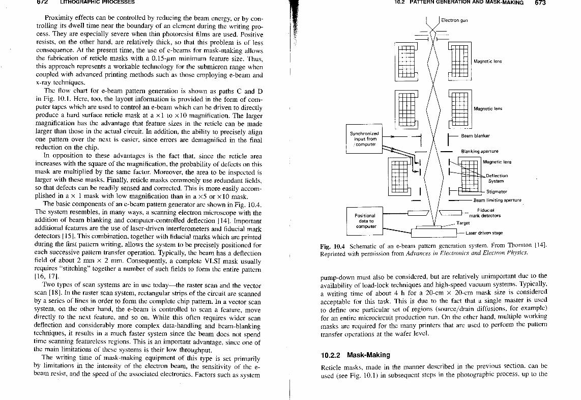
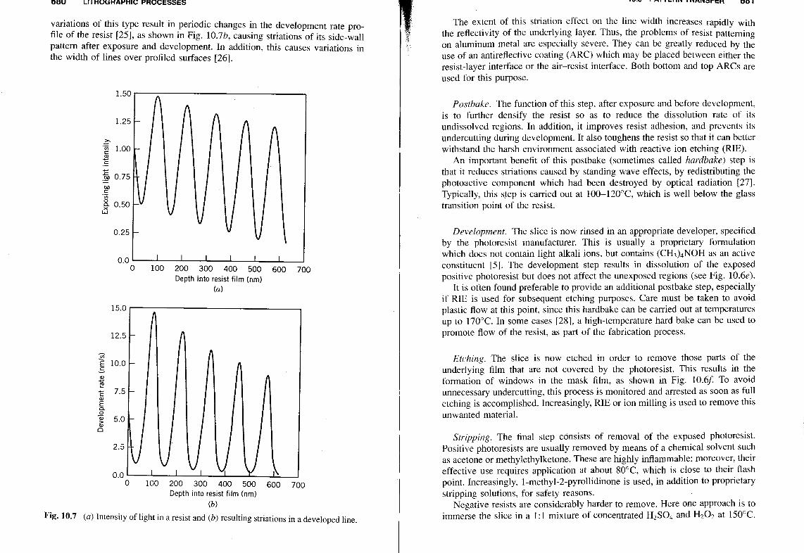
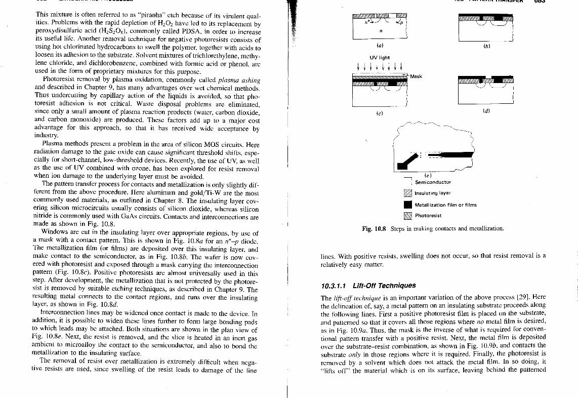
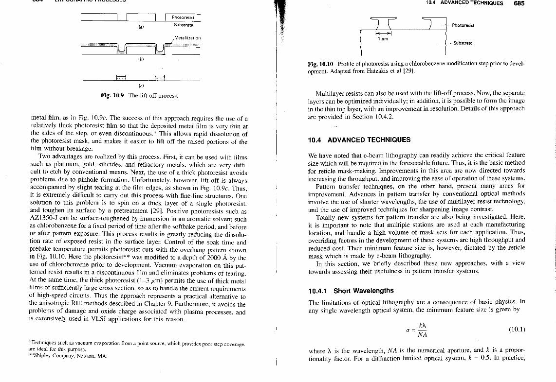
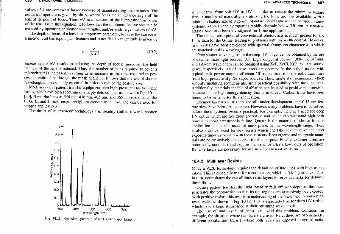
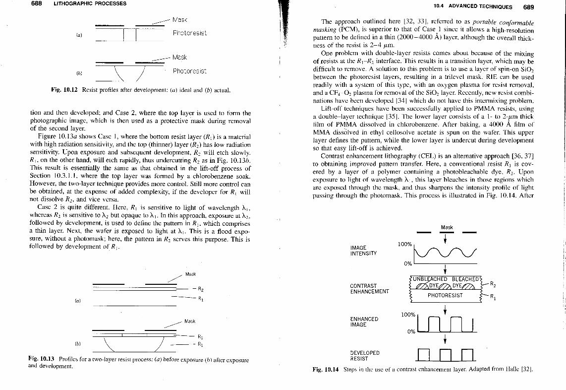
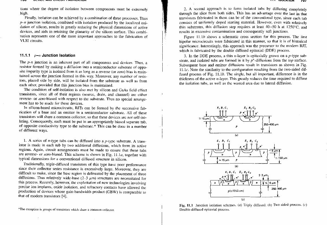
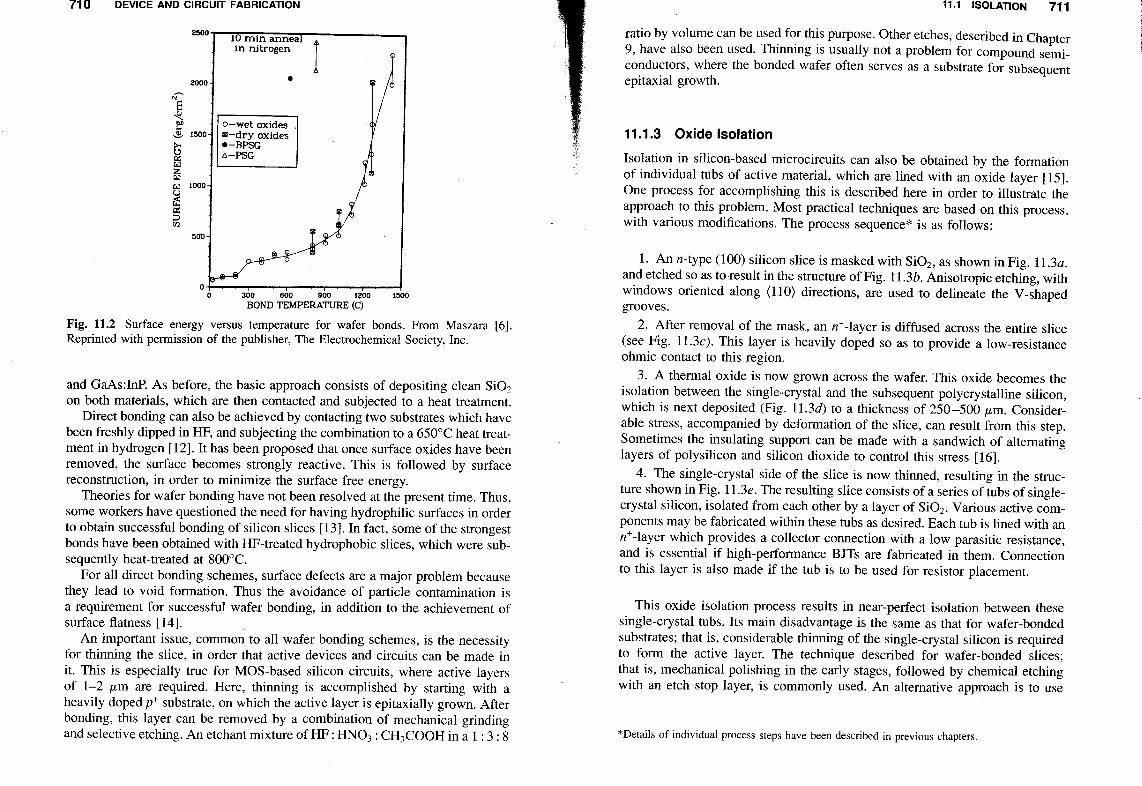
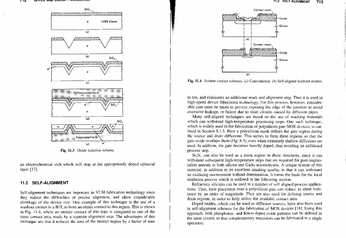
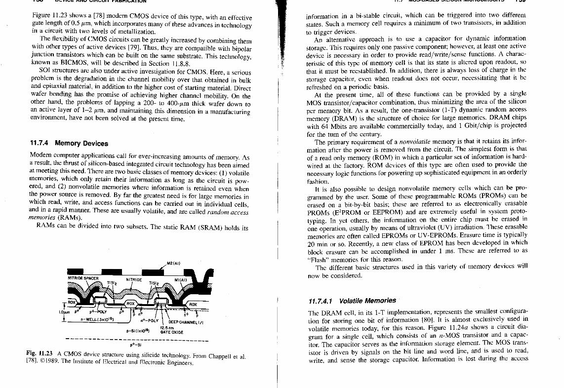
Upload aakansha-barnwal
View 329
Download 22
Embed Size (px) 344 x 292 429 x 357 514 x 422 599 x 487
Citation preview
05 Gallium Arsenide Technologies - Universiti Tunku Abdul Rahman
Gallium Arsenide Products Designers Information PDFapplication-notes.digchip.com/125/125-44618.pdf · 2009. 2. 8. · Gallium Arsenide Products Designers’ Information. TriQuint
Model Development for Lattice Properties of Gallium Arsenide using
A Gallium Arsenide MESFET Operational Amplifier for Use in Composite Operational Amplifiers
Studies of Electron Spin in Gallium Arsenide Quantum Dots
Activation Studies of Gallium Arsenide Photocathodes
ELECTRICAL PROPERTIES OF GALLIUM ARSENIDE ...epubs.surrey.ac.uk/847586/1/10800203.pdfABSTRACT The electrical properties of sulphur 32 implanted gallium arsenide were investigated using
The Gallium Arsenide Wafer Problem
Gallium Arsenide Thermal Conductivity and Optical Phonon
Model Development for Lattice Properties of Gallium Arsenide … · 2012. 10. 9. · Model Development for Lattice Properties of Gallium Arsenide using Parallel Genetic Algorithm
Document Number: MRFG35010A Technical Data Gallium ... · Gallium Arsenide PHEMT ... WLL/MMDS or UMTS driver and final applications. ... 0.70 0.958 176.7 3.578 74.8 0.0098 28.0 0.779
LDB, LSB, LE and LSE Series Linear Indium Gallium Arsenide
PHOTOLUMINESCENCE OF INDIUM GALLIUM … Jones... · PHOTOLUMINESCENCE OF INDIUM GALLIUM ARSENIDE QUANTUM DOTS AND DOT CHAINS by Aaron Mitchell Jones A senior thesis …
Cobalt in Hard Metals and Cobalt Sulfate, Gallium Arsenide ...€¦ · Cobalt in Hard Metals and Cobalt Sulfate, Gallium Arsenide, Indium Phosphide and Vanadium Pentoxide 00 i-iv
Structural and electronic properties of gallium arsenide ... · Structural and electronic properties of gallium arsenide crystal using INDO method Khalid H. B. AL-Ammar Fuaad Sh
Global Gallium Arsenide Devices Market 2016-2020
COHERENT NEAR INFRARED PHOTODETECTION WITH INDIUM GALLIUM ARSENIDE
Gallium arsenide based Buried Heterostructure Laser Diodes ...9091/FULLTEXT01.pdf · Gallium arsenide based Buried Heterostructure Laser Diodes with Aluminium-free Semi-Insulating
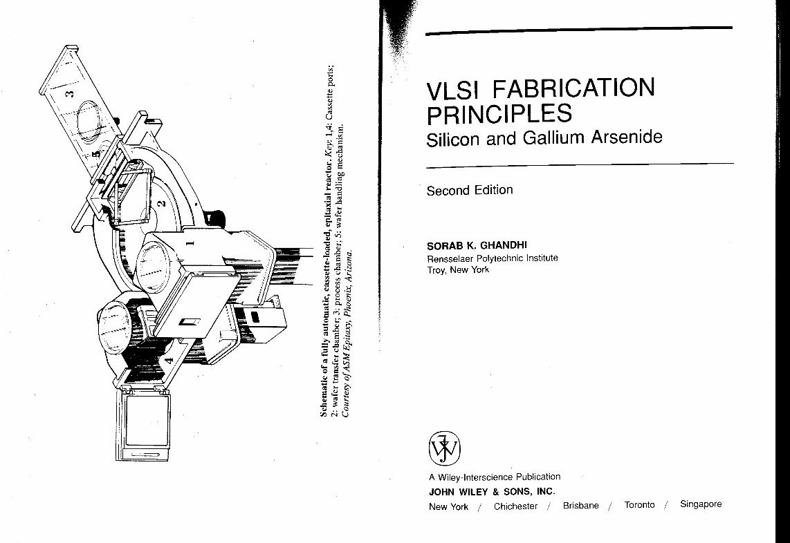
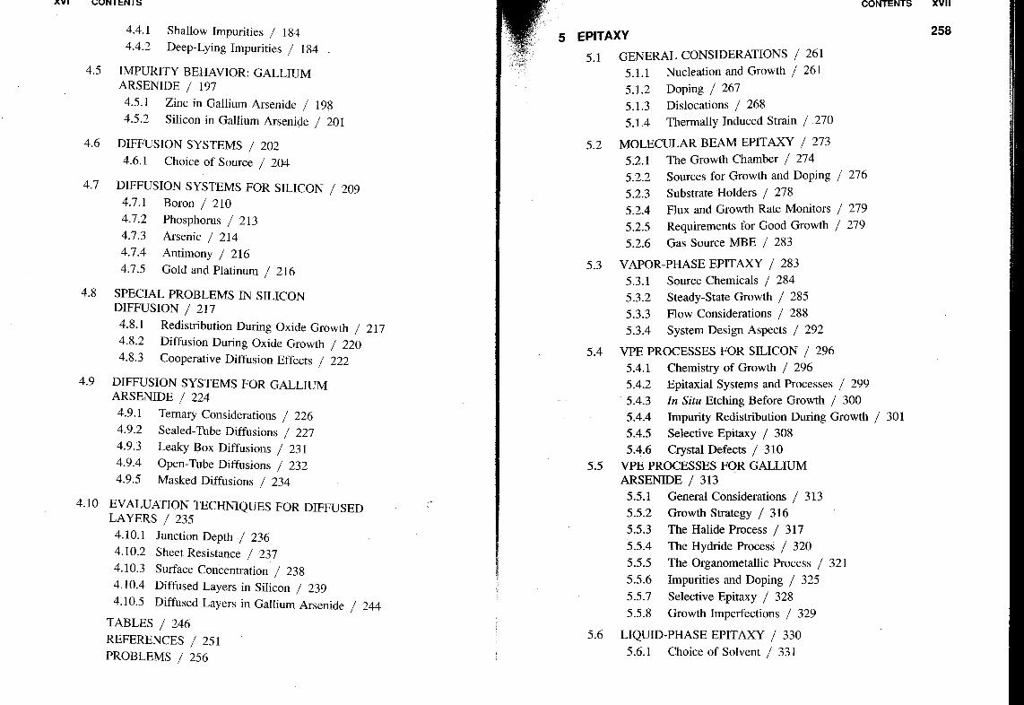
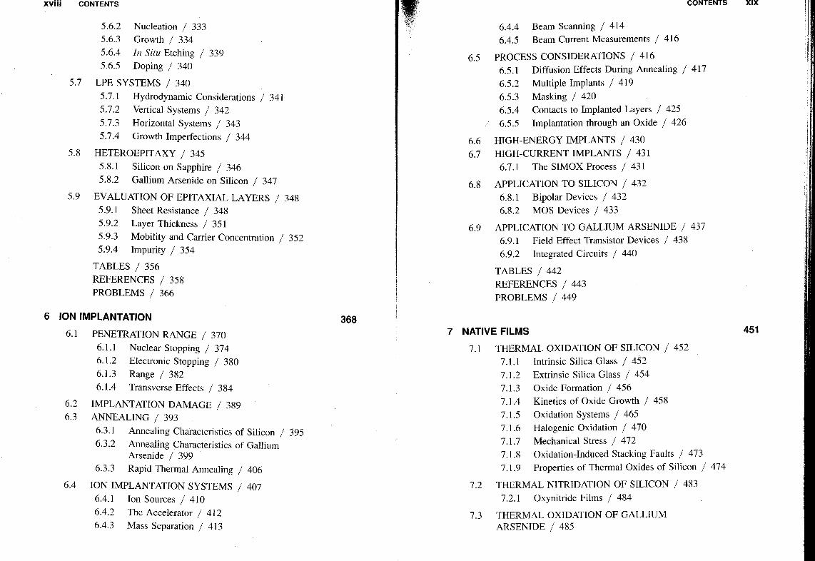
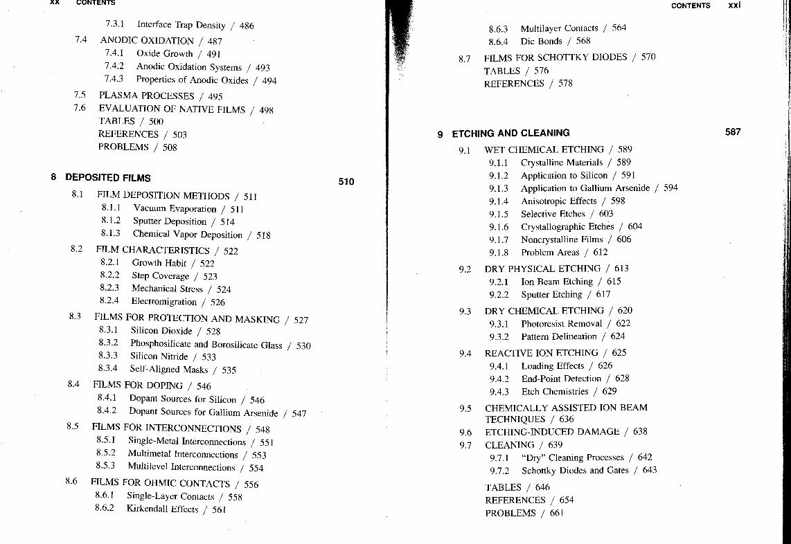
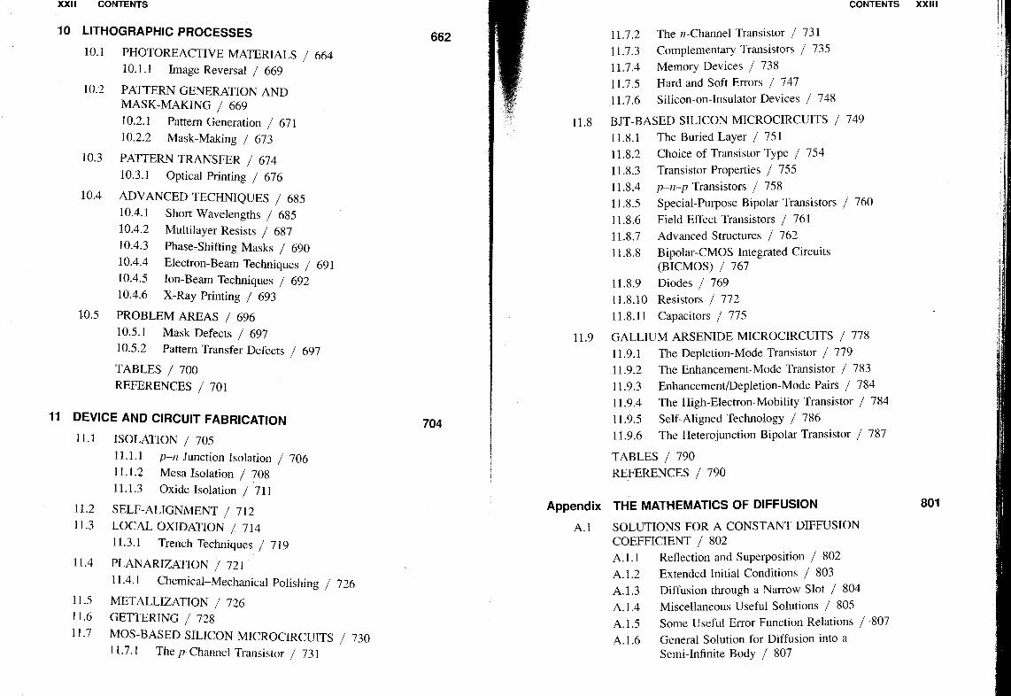
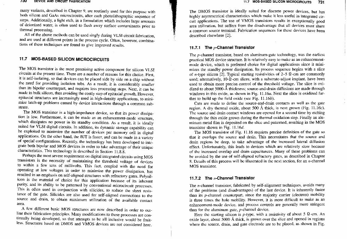
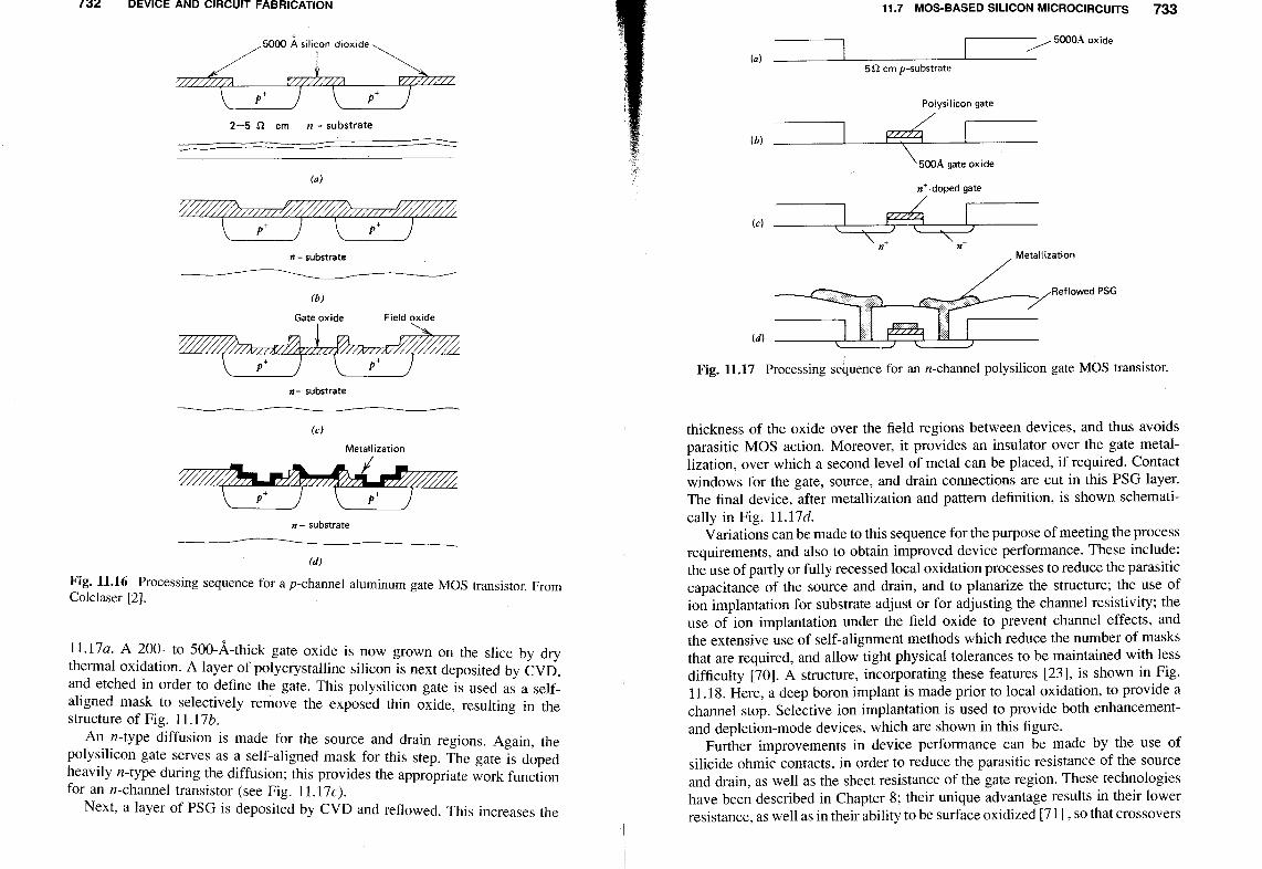
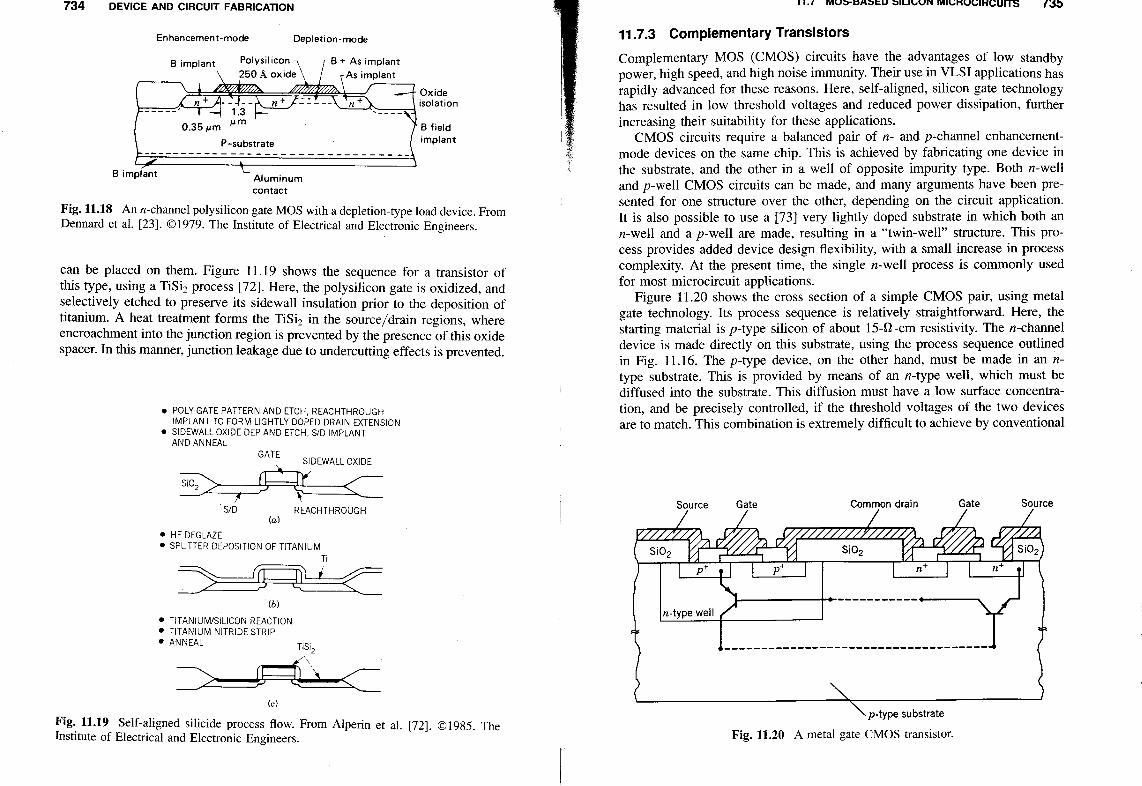
https___~avreddy_VLSI Fabrication Principles, Silicon and Gallium Arsenide - 1994 Ghandi (Wiley, 2E).pdf
Optimized (2nd Pass) Gallium Arsenide (GaAs) Integrated
Gallium Arsenide (GaAs) Microwave Integrated Circuit
Phase Transition and Elasticity of Gallium Arsenide under ... · Phase Transition and Elasticity of Gallium Arsenide under ... above 25 GPa and hexagonal cinnabar ... Phase Transition
Epitaxial growth of gallium arsenide - Philips Bound... · Gallium-arsenide microwave devices, in which epi- ... 107 ncm) is needed as an ... Epitaxial growth of gallium arsenide
Phase Transition and Elasticity of Gallium Arsenide under ... · Phase Transition and Elasticity of Gallium Arsenide under Pressure Since ductility and brittleness play a key role
Quasi-phase-matched gallium arsenide for - Optics InfoBase
World Semiconductor Council Anticounterfeiting Task Force · 2018-06-11 · Materials that partially conduct electricity •Typically silicon or gallium arsenide or gallium nitride
Unique Industrial Hygiene Aspects in Gallium Arsenide ... 2001 As IH Issues... · Unique Industrial Hygiene Aspects in Gallium Arsenide Device Manufacturing Facilities Author: Anthony
TRION MINILOCK III-V - UTA MINILOCK.pdf · The Trion Minilock II RIE (reactive ion etch) provides anisotropic plasma etching of Gallium Arsenide (GaAs), Aluminum Gallium Arsenide
Design and Study of Gallium Arsenide Optical Modulators
DEVELOPMENT OF IMPROVED GALLIUM ARSENIDE SOLAR CELLS Final … · Final Report I. INTRODUCTION A. History Interest in gallium arsenide solar cells was first aroused in 1955 when a