Embed Size (px)
Citation preview
Surface Science 606 (2012) 1221–1226
Contents lists available at SciVerse ScienceDirect
Surface Science
j ourna l homepage: www.e lsev ie r .com/ locate /susc
Stranski–Krastanow growth of copper overlayers on the Ni(110) surface
T. Fukuda a,⁎, K. Umezawa b, H. Nakayama a
a Department of Physical Electronics and Informatics, Graduate School of Engineering, Osaka City University, 3-3-138 Sugimoto, Sumiyoshi-Ku, Osaka 558-8585, Japanb Faculty of Liberal Arts and Sciences, Osaka Prefecture University, 1-1 Gakuen-cho, Naka-Ku, Sakai, Osaka 599-8531, Japan
⁎ Corresponding author. Tel.: +81 6 6605 2738; fax:E-mail address: [email protected] (
0039-6028/$ – see front matter © 2012 Elsevier B.V. Alldoi:10.1016/j.susc.2012.03.024
a b s t r a c t
a r t i c l e i n f oArticle history:Received 15 July 2011Accepted 30 March 2012Available online 5 April 2012
Keywords:Ni(110)CopperStranski–Krastanow growthSTMHeteroepitaxial growth
Cu overlayer formation on the Ni(110) surface was studied using scanning tunneling microscopy (STM) in anultrahigh vacuum. Room-temperature deposition of Cu onto a Ni(110) surface exhibited layer-by-layergrowth up to 6 monolayers (MLs), followed by three-dimensional island formation, i.e., the Cu overlayergrowth on the Ni(110) surface is classified as Stranski–Krastanow growth. At the initial growth stage, aniso-tropic two-dimensional islands were elongated in the close-packed 1�10
� �direction. The nucleation of the
second layer was strongly affected by the morphology of the first layer, and the second-layer islands alsoextended in the 1�10
� �direction. The third and further layers grew two-dimensionally. Detailed STM images
showed mosaic features due to Cu and Ni alloying. Three-dimensional islands were observed for Cu deposi-tion beyond 6 ML. The (110)-oriented top surface of the islands had stripes along the [001] direction. Inaddition, bumps extending in the 1�10
� �direction were formed on these island surfaces, indicating threading
dislocation through the island to relieve the compressive stress of the overlayers. An atomic model of thebump compatible with the STM image was proposed.
© 2012 Elsevier B.V. All rights reserved.
1. Introduction
Copper (Cu) and Nickel (Ni) are both fcc metals, and the lattice con-stant of bulk Cu is only 2.6% larger than that of Ni. Thus, Cu overlayerformation on Ni substrates and vice versa should show typical lattice-mismatched epitaxial growth. Contrary to this naive expectation, Cudeposition on a Ni(100) surface shows layer-by-layer growth up to 20monolayers (MLs) [1,2]. To relieve the compressive stress of epitaxialCu overlayers, one-dimensional dislocation is inserted even at thevery initial stage of the overlayer formation, and the dislocation extendsto become a threading dislocation with internal {111} faceting forthicker Cu films. The dislocation effectively decreases the compressivestress of Cu films, and the overlayer grows layer-by-layer up to 20MLs, indicating the complete Frank-van der Merwe growth mode. ForCu/Ni(100) surfaces, the interface between the Ni substrate and theCu overlayer will be sharp, and no intermixing is reported. However,we recently showed that Cu/Ni(110) exhibits clear evidence of Cu/Nimixing for fractional Cu overlayers through scanning tunnelingmicros-copy (STM) observation [3]. In this case, there is no degradation of crys-tallinity, such as dislocation or defect in the overlayers, so the overlayerwill be epitaxially grown with gradual decrease of the interfacial stressbymixing the substrate Ni into the overlayers. In this report, wewill ad-dress a breakdown of the epitaxial layer-by-layer growth at a critical
+81 6 6605 2738.T. Fukuda).
rights reserved.
thickness and three-dimensional island formation, which is termedthe Stranski–Krastanow growth.
2. Experimental
Since the experimental details were described previously [3], wewill simply give an overview here. An (110)-oriented Ni single crystalwas cleaned by repeated Ar+ ion sputtering and annealing in anultrahigh vacuum. Surface cleanliness was carefully examined usingSTM images prior to each Cu deposition. Cu was deposited onto theclean Ni(110) surface at room temperature at the rate of about 0.1ML/s, where 1 ML refers to the number of surface Ni atoms on theNi(110) surface. Cu coverage was determined using STM images. AllSTM images shown here were acquired at room temperature withthe constant current mode.
3. Results and discussion
3.1. Layer-by-layer growth
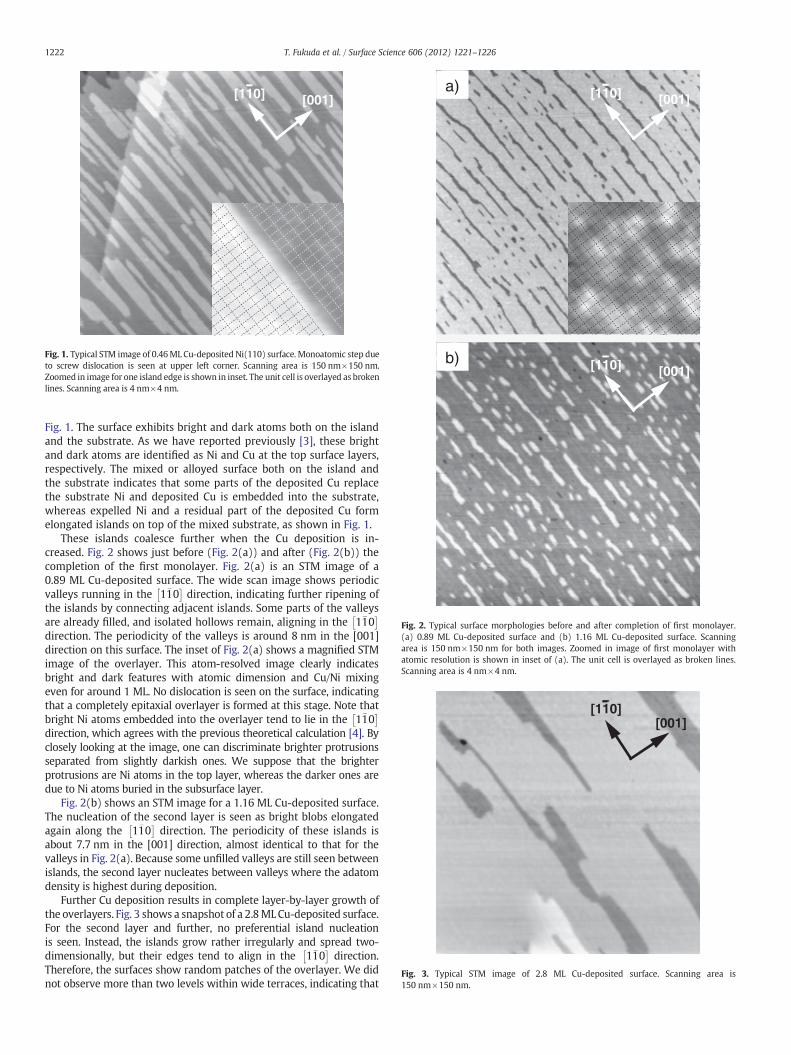
Typical surface morphology of a wide terrace of a 0.46 ML Cu-deposited surface is shown in Fig. 1. The surface exhibits anisotropicislands elongated along the close-packed [1�10] direction. All islandswere monatomic-layer high, and no multilayer island was formed.Some islands have already begun to coalesce, and they form widerislands in the [001] direction. Interestingly, some islands elongatedeven across a monatomic step located at the upper left in Fig. 1. Anatom-resolved image of an island edge is depicted in the inset of
[001][110]
Fig. 1. Typical STM image of 0.46ML Cu-deposited Ni(110) surface. Monoatomic step dueto screw dislocation is seen at upper left corner. Scanning area is 150 nm×150 nm.Zoomed in image for one island edge is shown in inset. The unit cell is overlayed as brokenlines. Scanning area is 4 nm×4 nm.
b)[001][110]
a)[001][110]
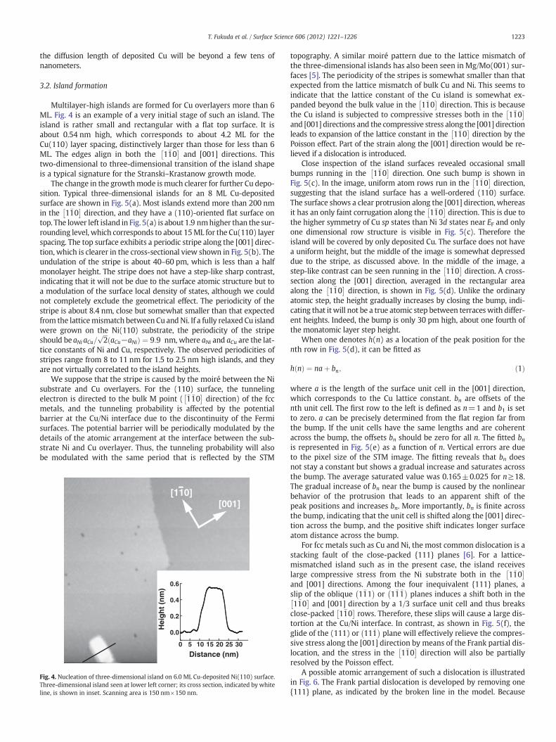
Fig. 2. Typical surface morphologies before and after completion of first monolayer.(a) 0.89 ML Cu-deposited surface and (b) 1.16 ML Cu-deposited surface. Scanningarea is 150 nm×150 nm for both images. Zoomed in image of first monolayer withatomic resolution is shown in inset of (a). The unit cell is overlayed as broken lines.Scanning area is 4 nm×4 nm.
[001][110]
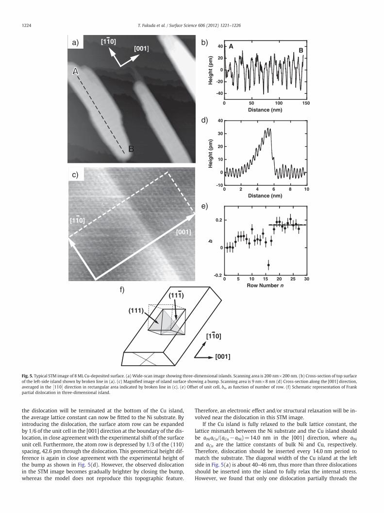
Fig. 3. Typical STM image of 2.8 ML Cu-deposited surface. Scanning area is150 nm×150 nm.
1222 T. Fukuda et al. / Surface Science 606 (2012) 1221–1226
Fig. 1. The surface exhibits bright and dark atoms both on the islandand the substrate. As we have reported previously [3], these brightand dark atoms are identified as Ni and Cu at the top surface layers,respectively. The mixed or alloyed surface both on the island andthe substrate indicates that some parts of the deposited Cu replacethe substrate Ni and deposited Cu is embedded into the substrate,whereas expelled Ni and a residual part of the deposited Cu formelongated islands on top of the mixed substrate, as shown in Fig. 1.
These islands coalesce further when the Cu deposition is in-creased. Fig. 2 shows just before (Fig. 2(a)) and after (Fig. 2(b)) thecompletion of the first monolayer. Fig. 2(a) is an STM image of a0.89 ML Cu-deposited surface. The wide scan image shows periodicvalleys running in the 1�10
� �direction, indicating further ripening of
the islands by connecting adjacent islands. Some parts of the valleysare already filled, and isolated hollows remain, aligning in the 1�10
� �
direction. The periodicity of the valleys is around 8 nm in the [001]direction on this surface. The inset of Fig. 2(a) shows a magnified STMimage of the overlayer. This atom-resolved image clearly indicatesbright and dark features with atomic dimension and Cu/Ni mixingeven for around 1 ML. No dislocation is seen on the surface, indicatingthat a completely epitaxial overlayer is formed at this stage. Note thatbright Ni atoms embedded into the overlayer tend to lie in the 1�10
� �
direction, which agrees with the previous theoretical calculation [4]. Byclosely looking at the image, one can discriminate brighter protrusionsseparated from slightly darkish ones. We suppose that the brighterprotrusions are Ni atoms in the top layer, whereas the darker ones aredue to Ni atoms buried in the subsurface layer.
Fig. 2(b) shows an STM image for a 1.16 ML Cu-deposited surface.The nucleation of the second layer is seen as bright blobs elongatedagain along the 1�10
� �direction. The periodicity of these islands is
about 7.7 nm in the [001] direction, almost identical to that for thevalleys in Fig. 2(a). Because some unfilled valleys are still seen betweenislands, the second layer nucleates between valleys where the adatomdensity is highest during deposition.
Further Cu deposition results in complete layer-by-layer growth ofthe overlayers. Fig. 3 shows a snapshot of a 2.8MLCu-deposited surface.For the second layer and further, no preferential island nucleationis seen. Instead, the islands grow rather irregularly and spread two-dimensionally, but their edges tend to align in the 1�10
� �direction.
Therefore, the surfaces show random patches of the overlayer. We didnot observe more than two levels within wide terraces, indicating that
1223T. Fukuda et al. / Surface Science 606 (2012) 1221–1226
the diffusion length of deposited Cu will be beyond a few tens ofnanometers.
3.2. Island formation
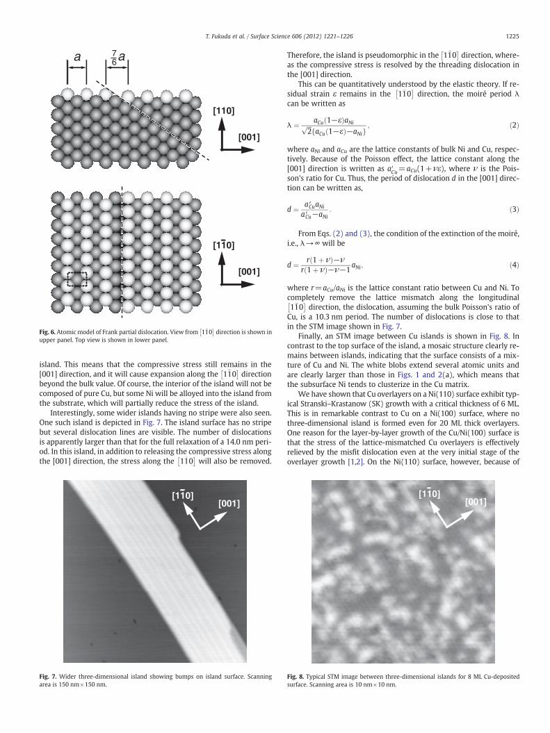
Multilayer-high islands are formed for Cu overlayers more than 6ML. Fig. 4 is an example of a very initial stage of such an island. Theisland is rather small and rectangular with a flat top surface. It isabout 0.54 nm high, which corresponds to about 4.2 ML for theCu(110) layer spacing, distinctively larger than those for less than 6ML. The edges align in both the 1�10
� �and [001] directions. This
two-dimensional to three-dimensional transition of the island shapeis a typical signature for the Stranski–Krastanow growth mode.
The change in the growthmode ismuch clearer for further Cu depo-sition. Typical three-dimensional islands for an 8 ML Cu-depositedsurface are shown in Fig. 5(a). Most islands extend more than 200 nmin the 1�10
� �direction, and they have a (110)-oriented flat surface on
top. The lower left island in Fig. 5(a) is about 1.9 nmhigher than the sur-rounding level, which corresponds to about 15ML for the Cu(110) layerspacing. The top surface exhibits a periodic stripe along the [001] direc-tion, which is clearer in the cross-sectional view shown in Fig. 5(b). Theundulation of the stripe is about 40–60 pm, which is less than a halfmonolayer height. The stripe does not have a step-like sharp contrast,indicating that it will not be due to the surface atomic structure but toa modulation of the surface local density of states, although we couldnot completely exclude the geometrical effect. The periodicity of thestripe is about 8.4 nm, close but somewhat smaller than that expectedfrom the latticemismatch between Cu andNi. If a fully relaxed Cu islandwere grown on the Ni(110) substrate, the periodicity of the stripeshould be aNi aCu=
ffiffiffi2
paCu−aNið Þ ¼ 9:9 nm, where aNi and aCu are the lat-
tice constants of Ni and Cu, respectively. The observed periodicities ofstripes range from 8 to 11 nm for 1.5 to 2.5 nm high islands, and theyare not virtually correlated to the island heights.
We suppose that the stripe is caused by the moiré between the Nisubstrate and Cu overlayers. For the (110) surface, the tunnelingelectron is directed to the bulk M point ( �1�10
� �direction) of the fcc
metals, and the tunneling probability is affected by the potentialbarrier at the Cu/Ni interface due to the discontinuity of the Fermisurfaces. The potential barrier will be periodically modulated by thedetails of the atomic arrangement at the interface between the sub-strate Ni and Cu overlayer. Thus, the tunneling probability will alsobe modulated with the same period that is reflected by the STM
0.2
0.4
0.6
0 5 10 15 20 25 30
Hei
gh
t (n
m)
Distance (nm)
0.0
[001][110]
Fig. 4. Nucleation of three-dimensional island on 6.0 ML Cu-deposited Ni(110) surface.Three-dimensional island seen at lower left corner; its cross section, indicated by whiteline, is shown in inset. Scanning area is 150 nm×150 nm.
topography. A similar moiré pattern due to the lattice mismatch ofthe three-dimensional islands has also been seen in Mg/Mo(001) sur-faces [5]. The periodicity of the stripes is somewhat smaller than thatexpected from the lattice mismatch of bulk Cu and Ni. This seems toindicate that the lattice constant of the Cu island is somewhat ex-panded beyond the bulk value in the 1�10
� �direction. This is because
the Cu island is subjected to compressive stresses both in the 1�10� �
and [001] directions and the compressive stress along the [001] directionleads to expansion of the lattice constant in the 1�10
� �direction by the
Poisson effect. Part of the strain along the [001] direction would be re-lieved if a dislocation is introduced.
Close inspection of the island surfaces revealed occasional smallbumps running in the 1�10
� �direction. One such bump is shown in
Fig. 5(c). In the image, uniform atom rows run in the 1�10� �
direction,suggesting that the island surface has a well-ordered (110) surface.The surface shows a clear protrusion along the [001] direction, whereasit has an only faint corrugation along the 1�10
� �direction. This is due to
the higher symmetry of Cu sp states than Ni 3d states near EF and onlyone dimensional row structure is visible in Fig. 5(c). Therefore theisland will be covered by only deposited Cu. The surface does not havea uniform height, but the middle of the image is somewhat depresseddue to the stripe, as discussed above. In the middle of the image, astep-like contrast can be seen running in the 1�10
� �direction. A cross-
section along the [001] direction, averaged in the rectangular areaalong the 1�10
� �direction, is shown in Fig. 5(d). Unlike the ordinary
atomic step, the height gradually increases by closing the bump, indi-cating that it will not be a true atomic step between terraceswith differ-ent heights. Indeed, the bump is only 30 pm high, about one fourth ofthe monatomic layer step height.
When one denotes h(n) as a location of the peak position for thenth row in Fig. 5(d), it can be fitted as
h nð Þ ¼ naþ bn; ð1Þ
where a is the length of the surface unit cell in the [001] direction,which corresponds to the Cu lattice constant. bn are offsets of thenth unit cell. The first row to the left is defined as n=1 and b1 is setto zero. a can be precisely determined from the flat region far fromthe bump. If the unit cells have the same lengths and are coherentacross the bump, the offsets bn should be zero for all n. The fitted bnis represented in Fig. 5(e) as a function of n. Vertical errors are dueto the pixel size of the STM image. The fitting reveals that bn doesnot stay a constant but shows a gradual increase and saturates acrossthe bump. The average saturated value was 0.165±0.025 for n≥18.The gradual increase of bn near the bump is caused by the nonlinearbehavior of the protrusion that leads to an apparent shift of thepeak positions and increases bn. More importantly, bn is finite acrossthe bump, indicating that the unit cell is shifted along the [001] direc-tion across the bump, and the positive shift indicates longer surfaceatom distance across the bump.
For fcc metals such as Cu and Ni, the most common dislocation is astacking fault of the close-packed {111} planes [6]. For a lattice-mismatched island such as in the present case, the island receiveslarge compressive stress from the Ni substrate both in the 1�10
� �
and [001] directions. Among the four inequivalent {111} planes, aslip of the oblique 1�11
� �or 1�1�1
� �planes induces a shift both in the
1�10� �
and [001] direction by a 1/3 surface unit cell and thus breaksclose-packed 1�10
� �rows. Therefore, these slips will cause a large dis-
tortion at the Cu/Ni interface. In contrast, as shown in Fig. 5(f), theglide of the (111) or 11�1
� �plane will effectively relieve the compres-
sive stress along the [001] direction by means of the Frank partial dis-location, and the stress in the 1�10
� �direction will also be partially
resolved by the Poisson effect.A possible atomic arrangement of such a dislocation is illustrated
in Fig. 6. The Frank partial dislocation is developed by removing one{111} plane, as indicated by the broken line in the model. Because
AA
B
[001][110]a) A
Bb)
-40
-20
0
20
40
0 50 100 150
Hei
gh
t (p
m)
Distance (nm)
[001]
[110]
c)-10
0
10
20
30
40
0 2 4 6 8 10
Hei
gh
t (p
m)
Distance (nm)
d)
-0.2
0
0.2
0 5 10 15 20 25 30
b
Row Number n
e)
[001]
[110]
(111)
(111)f)
Fig. 5. Typical STM image of 8 ML Cu-deposited surface. (a) Wide-scan image showing three-dimensional islands. Scanning area is 200 nm×200 nm. (b) Cross-section of top surfaceof the left-side island shown by broken line in (a). (c) Magnified image of island surface showing a bump. Scanning area is 9 nm×8 nm (d) Cross-section along the [001] direction,averaged in the 1�10
� �direction in rectangular area indicated by broken line in (c). (e) Offset of unit cell, bn, as function of number of row. (f) Schematic representation of Frank
partial dislocation in three-dimensional island.
1224 T. Fukuda et al. / Surface Science 606 (2012) 1221–1226
the dislocation will be terminated at the bottom of the Cu island,the average lattice constant can now be fitted to the Ni substrate. Byintroducing the dislocation, the surface atom row can be expandedby 1/6 of the unit cell in the [001] direction at the boundary of the dis-location, in close agreement with the experimental shift of the surfaceunit cell. Furthermore, the atom row is depressed by 1/3 of the (110)spacing, 42.6 pm through the dislocation. This geometrical height dif-ference is again in close agreement with the experimental height ofthe bump as shown in Fig. 5(d). However, the observed dislocationin the STM image becomes gradually brighter by closing the bump,whereas the model does not reproduce this topographic feature.
Therefore, an electronic effect and/or structural relaxation will be in-volved near the dislocation in this STM image.
If the Cu island is fully relaxed to the bulk lattice constant, thelattice mismatch between the Ni substrate and the Cu island shouldbe aNiaCu/(aCu−aNi)=14.0 nm in the [001] direction, where aNiand aCu are the lattice constants of bulk Ni and Cu, respectively.Therefore, dislocation should be inserted every 14.0 nm period tomatch the substrate. The diagonal width of the Cu island at the leftside in Fig. 5(a) is about 40–46 nm, thus more than three dislocationsshould be inserted into the island to fully relax the internal stress.However, we found that only one dislocation partially threads the
a a67
[001]
[110]
[001]
[110]
Fig. 6. Atomic model of Frank partial dislocation. View from 1�10� �
direction is shown inupper panel. Top view is shown in lower panel.
1225T. Fukuda et al. / Surface Science 606 (2012) 1221–1226
island. This means that the compressive stress still remains in the[001] direction, and it will cause expansion along the 1�10
� �direction
beyond the bulk value. Of course, the interior of the island will not becomposed of pure Cu, but some Ni will be alloyed into the island fromthe substrate, which will partially reduce the stress of the island.
Interestingly, some wider islands having no stripe were also seen.One such island is depicted in Fig. 7. The island surface has no stripebut several dislocation lines are visible. The number of dislocationsis apparently larger than that for the full relaxation of a 14.0 nm peri-od. In this island, in addition to releasing the compressive stress alongthe [001] direction, the stress along the 1�10
� �will also be removed.
[001][110]
Fig. 7. Wider three-dimensional island showing bumps on island surface. Scanningarea is 150 nm×150 nm.
Therefore, the island is pseudomorphic in the 1�10� �
direction, where-as the compressive stress is resolved by the threading dislocation inthe [001] direction.
This can be quantitatively understood by the elastic theory. If re-sidual strain ε remains in the 1�10
� �direction, the moiré period λ
can be written as
λ ¼ aCu 1−εð ÞaNiffiffiffi2
paCu 1−εð Þ−aNif g ; ð2Þ
where aNi and aCu are the lattice constants of bulk Ni and Cu, respec-tively. Because of the Poisson effect, the lattice constant along the[001] direction is written as a′Cu=aCu(1+νε), where ν is the Pois-son's ratio for Cu. Thus, the period of dislocation d in the [001] direc-tion can be written as,
d ¼ a′CuaNia′Cu−aNi
: ð3Þ
From Eqs. (2) and (3), the condition of the extinction of the moiré,i.e., λ→∞ will be
d ¼ r 1þ νð Þ−νr 1þ νð Þ−ν−1
aNi; ð4Þ
where r=aCu/aNi is the lattice constant ratio between Cu and Ni. Tocompletely remove the lattice mismatch along the longitudinal1�10� �
direction, the dislocation, assuming the bulk Poisson's ratio ofCu, is a 10.3 nm period. The number of dislocations is close to thatin the STM image shown in Fig. 7.
Finally, an STM image between Cu islands is shown in Fig. 8. Incontrast to the top surface of the island, a mosaic structure clearly re-mains between islands, indicating that the surface consists of a mix-ture of Cu and Ni. The white blobs extend several atomic units andare clearly larger than those in Figs. 1 and 2(a), which means thatthe subsurface Ni tends to clusterize in the Cu matrix.
We have shown that Cu overlayers on a Ni(110) surface exhibit typ-ical Stranski–Krastanow (SK) growth with a critical thickness of 6 ML.This is in remarkable contrast to Cu on a Ni(100) surface, where nothree-dimensional island is formed even for 20 ML thick overlayers.One reason for the layer-by-layer growth of the Cu/Ni(100) surface isthat the stress of the lattice-mismatched Cu overlayers is effectivelyrelieved by the misfit dislocation even at the very initial stage of theoverlayer growth [1,2]. On the Ni(110) surface, however, because of
[001][110]
Fig. 8. Typical STM image between three-dimensional islands for 8 ML Cu-depositedsurface. Scanning area is 10 nm×10 nm.
1226 T. Fukuda et al. / Surface Science 606 (2012) 1221–1226
the strong anisotropy of the surface and interface structures, the stressexerted by the substrate cannot be effectively removed unless disloca-tion with a large distortion is introduced. Instead, mixing of substrateNi into the overlayer reduces the interfacial stress to some extent. How-ever, this Cu/Ni mixing is a kinetic process and will dwindle for thickeroverlayers. Thus, stress accumulates in the overlayer and finally three-dimensional islands grow. Because of themixing of Ni into the Cu over-layer, layer-by-layer growth is prolonged until 6 ML, even though thedislocation energy is fairly small [6].
Many combinations of metal substrates with dissimilar metaloverlayers have been found to show SK growth. Aside from earlystudies using element-sensitive but poor spatial-resolved techniquessuch as Auger electron spectroscopy (AES) and x-ray photoelectronspectroscopy (XPS), recent STM and low energy electron microscopy(LEEM) studies unambiguously proved SK growth of some metalcombinations, such as Cr/W(100) [7], Mg/Mo(100) [5], Fe/Mo(110)[8], Pb,Sn/Rh(111) [9], Co/W(111) [10], Ag, Au/Mo(111) [11], andFe/W(110) [12]. For most cases, the overlayers and the substrateshave different crystal symmetries, and the surface atomic structuresof the wetting layer do not resemble those of the bulk low indexfaces of the overlayer metals. Therefore, epitaxial growth of the over-layer seems to be inherently quite difficult. In particular, for noblemetal overlayers on refractory metal substrates such as Au/Mo(111)[11], the surface free energy of the refractory metal substrate isusually much higher than that of the noble metal overlayers. Thissometimes induces instability of the overlayer and results in facetingand the surface exhibiting pyramid-like structures [11,13]. Even for abcc combination such as Cr/W(100), the lattice mismatch is very large(−8.8%) and thus the critical thickness of the SK growth is only 3 ML.Similarly, fcc combinations such as Pb/Rh(111) and Sn/Rh(111) alsohave large lattice mismatches (+33 and +74% for Pb/Rh and Sn/Rh,respectively). In contrast to these metals, both Cu and Ni have fccstructures with a marginal difference in the lattice constant. Further-more, the wetting layer has no superstructure and the transition fromthe two-dimensional to three-dimensional growth is purely governedby the stress of the overlayers.
In this respect, the Cu/Ni(110) growth resembles semiconductorheteroepitaxial growths, in particular growths of Group IV semiconduc-tors such asGe/Si [14]. BothGe/Si(111) andGe/Si(100) show SK growthwith interlayer mixing [14,15]. Initially, two-dimensional pseudomor-phic Ge overlayers grow to a few monolayers. At this stage, a part of Siin the substrate is incorporated into the Ge overlayers with displaciveadsorption [16]. Therefore, the wetting overlayers become composedof both Ge and Si. Beyond the critical thicknesses, pseudomorphicthree-dimensional islands emerge, followed by the internal strain ofthe island being relieved by threading dislocation. Unlike Cu/Ni(110),Ge wetting layers exhibit 2×n and 5×5 superstructures for Ge/Si(100) and Ge/Si(111), respectively, to relieve interfacial stresses andto lower the surface free energies. Although Ge/Si(100) exhibits uniquekinetic pathway known as the hut cluster [17], the overall features of itsSK growth resemble those of Cu/Ni(110).
We should also comment on a previous XPS study combined withion scattering spectroscopy (ISS) and AES for Cu/Ni(110) surfaces [18].ISS induces sputtering of the surface layers, and the time-dependentISS corresponds to a depth profile of the sample. Therefore, decreaseof Cu and increase of Ni for a 9 ML-thick Cu overlayer in a relativelyshort time suggest Ni being situated near the surface region [18]. Fur-thermore, photoelectron spectroscopy (PES) for a sample of a 40 ML-
thick Cu overlayer formed on Ni(110) still shows a significant Ni 3dpeak near EF [18]. These features are compatible with the SK growth ofthe Cu/Ni(110) surface.
4. Conclusion
We have shown that Cu overlayer formation on Ni(110) exhibitstypical Stranski–Krastanow growth with a critical thickness of 6 ML.Initially deposited Cu forms anisotropic two-dimensional islands alongthe 1�10
� �direction. Because part of the deposited Cu is embedded
into the top Ni substrate layer, repelled Ni is incorporated into Cuislands. The nucleation of the second layer is strongly affected by thesurface morphology of the first layer, but following overlayers extendtwo-dimensionally with complete layer-by-layer growth up to 6 ML.
Atomistic observation of the surface indicates that Cu/Ni mixing isnot limited to the first monolayer, which is a counterexample of thestrong tendency of Cu segregation on Cu/Ni alloy surfaces [19–21].Furthermore, in contrast to the Cu/Ni(100) surface, the epitaxially-grown wetting layers on the Ni(110) surface do not show any recon-struction or dislocation.
Three-dimensional islands emerge for the Cu overlayer beyond 6ML. Stripe structures are seen on top of these islands along the [001]direction, and they are due to a moiré pattern caused by the latticemismatch between the Ni substrate and the Cu overlayer. In addition,bumps running in the 1�10
� �direction are also seen on the islands.
They are caused by the threading dislocation in the {111} planes forreducing the compressive stress of the three-dimensional Cu islands.Some islands are fully relaxed and pseudomorphic only in the 1�10
� �
direction, but many threading dislocations resolve the compressivestresses both in the [001] and 1�10
� �directions by the Poisson effect.
References
[1] Bert Müller, Bjørn Fischer, Lorentz Nedelmann, Alexander Fricke, Klaus Kern,Phys. Rev. Lett. 76 (1996) 2358.
[2] Bert Müller, Lorentz Nedelmann, Bjørn Fischer, Alexander Fricke, Klaus Kern,J. Vac. Sci. Technol. A 14 (1996) 1878.
[3] T. Fukuda, K. Iwamoto, K. Umezawa, H. Nakayama, Phys. Rev. B78 (2008) 195422.[4] T. Fukuda, K. Umezawa, I. Kishida, H. Nakayama, E-J. Surf. Sci. Nanotech. 7 (2009)
681.[5] M.C. Gallagher, M.S. Fyfield, S.A. Joyce, Phys. Rev. B59 (1999) 2346.[6] A. Kelly, G.W. Groves, P. Kidd, Crystallography and Crystal defects, Revised Edition,
Wiley, NJ, 2000.[7] K.L. Man, Q. Guo, M.S. Altman, Surf. Sci. 600 (2006) 1060.[8] J. Osing, I.V. Shvets, Surf. Sci. 433–435 (1999) 440.[9] J. Yuhara, M. Schmid, P. Varga, Phys. Rev. B67 (2003) 195407.
[10] K.L. Man, R. Zdyb, S.F. Huang, T.C. Leung, C.T. Chan, E. Bauer, M.S. Altman, Phys.Rev. B67 (2003) 184402.
[11] D.B. Dańko, M. Kuchowicz, R. Szukiewicz, J. Kołaczkiewicz, Surf. Sci. 600 (2006)2258.
[12] H. Bethge, D. Heuer, Ch. Jensen, K. Reshöft, U. Köhler, Surf. Sci. 331–333 (1995)878.
[13] Theodore E. Madey, Jie Guan, Cheng-Zhi Dong, S.M. Shivaprasad, Surf. Sci.287–288 (1993) 826.
[14] Bert Voigtlander, Surf. Sci. Rep. 43 (2001) 127.[15] L. Patthey, E.L. Bullock, T. Abukawa, S. Kono, L.S.O. Johanssen, Phys. Rev. Lett. 75
(1995) 2538.[16] R.M. Tromp, Phys. Rev. B47 (1993) 7125.[17] Y.-W. Mo, D.E. Savage, B.S. Swartzentruber, M.F. Lagally, Phys. Rev. Lett. 65 (1990)
1020.[18] V. Rogge, H. Neddermeyer, Phys. Rev. B40 (1989) 7559.[19] Yee S. Ng, T.T. Tsong, S.B. McLane Jr., Phys. Rev. Lett. 42 (1979) 588.[20] Yee S. Ng, T.T. Tsong, S.B. McLane Jr., Surf. Sci. 84 (1979) 31.[21] Toshio Sakurai, T. Hashizume, A. Jimbo, A. Sakai, Phys. Rev. Lett. 55 (1985) 514.