Embed Size (px)
Citation preview
DAQ M SeriesNI USB-621x User ManualBus-Powered M Series USB Devices
NI USB-621x User Manual
ni.com/manuals
DeutschFrançais
March 2008371931E-01
Support
Worldwide Technical Support and Product Information
ni.com
National Instruments Corporate Headquarters
11500 North Mopac Expressway Austin, Texas 78759-3504 USA Tel: 512 683 0100
Worldwide Offices
Australia 1800 300 800, Austria 43 662 457990-0, Belgium 32 (0) 2 757 0020, Brazil 55 11 3262 3599, Canada 800 433 3488, China 86 21 5050 9800, Czech Republic 420 224 235 774, Denmark 45 45 76 26 00, Finland 358 (0) 9 725 72511, France 01 57 66 24 24, Germany 49 89 7413130, India 91 80 41190000, Israel 972 3 6393737, Italy 39 02 41309277, Japan 0120-527196, Korea 82 02 3451 3400, Lebanon 961 (0) 1 33 28 28, Malaysia 1800 887710, Mexico 01 800 010 0793, Netherlands 31 (0) 348 433 466, New Zealand 0800 553 322, Norway 47 (0) 66 90 76 60, Poland 48 22 3390150, Portugal 351 210 311 210, Russia 7 495 783 6851, Singapore 1800 226 5886, Slovenia 386 3 425 42 00, South Africa 27 0 11 805 8197, Spain 34 91 640 0085, Sweden 46 (0) 8 587 895 00, Switzerland 41 56 2005151, Taiwan 886 02 2377 2222, Thailand 662 278 6777, Turkey 90 212 279 3031, United Kingdom 44 (0) 1635 523545
For further support information, refer to the Technical Support and Professional Services appendix. To comment on National Instruments documentation, refer to the National Instruments Web site at ni.com/info and enter the info code feedback.
© 2006–2008 National Instruments Corporation. All rights reserved.
Important Information
WarrantyThe NI USB-6210, NI USB-6211, NI USB-6212, NI USB-6215, NI USB-6216, and NI USB-6218 are warranted against defects in materials and workmanship for a period of one year from the date of shipment, as evidenced by receipts or other documentation. National Instruments will, at its option, repair or replace equipment that proves to be defective during the warranty period. This warranty includes parts and labor.
The media on which you receive National Instruments software are warranted not to fail to execute programming instructions, due to defects in materials and workmanship, for a period of 90 days from date of shipment, as evidenced by receipts or other documentation. National Instruments will, at its option, repair or replace software media that do not execute programming instructions if National Instruments receives notice of such defects during the warranty period. National Instruments does not warrant that the operation of the software shall be uninterrupted or error free.
A Return Material Authorization (RMA) number must be obtained from the factory and clearly marked on the outside of the package before any equipment will be accepted for warranty work. National Instruments will pay the shipping costs of returning to the owner parts which are covered by warranty.
National Instruments believes that the information in this document is accurate. The document has been carefully reviewed for technical accuracy. In the event that technical or typographical errors exist, National Instruments reserves the right to make changes to subsequent editions of this document without prior notice to holders of this edition. The reader should consult National Instruments if errors are suspected. In no event shall National Instruments be liable for any damages arising out of or related to this document or the information contained in it.
EXCEPT AS SPECIFIED HEREIN, NATIONAL INSTRUMENTS MAKES NO WARRANTIES, EXPRESS OR IMPLIED, AND SPECIFICALLY DISCLAIMS ANY WARRANTY OF MERCHANTABILITY OR FITNESS FOR A PARTICULAR PURPOSE. CUSTOMER’S RIGHT TO RECOVER DAMAGES CAUSED BY FAULT OR NEGLIGENCE ON THE PART OF NATIONAL INSTRUMENTS SHALL BE LIMITED TO THE AMOUNT THERETOFORE PAID BY THE CUSTOMER. NATIONAL INSTRUMENTS WILL NOT BE LIABLE FOR DAMAGES RESULTING FROM LOSS OF DATA, PROFITS, USE OF PRODUCTS, OR INCIDENTAL OR CONSEQUENTIAL DAMAGES, EVEN IF ADVISED OF THE POSSIBILITY THEREOF. This limitation of the liability of National Instruments will apply regardless of the form of action, whether in contract or tort, including negligence. Any action against National Instruments must be brought within one year after the cause of action accrues. National Instruments shall not be liable for any delay in performance due to causes beyond its reasonable control. The warranty provided herein does not cover damages, defects, malfunctions, or service failures caused by owner’s failure to follow the National Instruments installation, operation, or maintenance instructions; owner’s modification of the product; owner’s abuse, misuse, or negligent acts; and power failure or surges, fire, flood, accident, actions of third parties, or other events outside reasonable control.
CopyrightUnder the copyright laws, this publication may not be reproduced or transmitted in any form, electronic or mechanical, including photocopying, recording, storing in an information retrieval system, or translating, in whole or in part, without the prior written consent of National Instruments Corporation.
National Instruments respects the intellectual property of others, and we ask our users to do the same. NI software is protected by copyright and other intellectual property laws. Where NI software may be used to reproduce software or other materials belonging to others, you may use NI software only to reproduce materials that you may reproduce in accordance with the terms of any applicable license or other legal restriction.
TrademarksNational Instruments, NI, ni.com, and LabVIEW are trademarks of National Instruments Corporation. Refer to the Terms of Use section on ni.com/legal for more information about National Instruments trademarks.
Other product and company names mentioned herein are trademarks or trade names of their respective companies.
Members of the National Instruments Alliance Partner Program are business entities independent from National Instruments and have no agency, partnership, or joint-venture relationship with National Instruments.
PatentsFor patents covering National Instruments products, refer to the appropriate location: Help»Patents in your software, the patents.txt file on your CD, or ni.com/patents.
WARNING REGARDING USE OF NATIONAL INSTRUMENTS PRODUCTS(1) NATIONAL INSTRUMENTS PRODUCTS ARE NOT DESIGNED WITH COMPONENTS AND TESTING FOR A LEVEL OF RELIABILITY SUITABLE FOR USE IN OR IN CONNECTION WITH SURGICAL IMPLANTS OR AS CRITICAL COMPONENTS IN ANY LIFE SUPPORT SYSTEMS WHOSE FAILURE TO PERFORM CAN REASONABLY BE EXPECTED TO CAUSE SIGNIFICANT INJURY TO A HUMAN.
(2) IN ANY APPLICATION, INCLUDING THE ABOVE, RELIABILITY OF OPERATION OF THE SOFTWARE PRODUCTS CAN BE IMPAIRED BY ADVERSE FACTORS, INCLUDING BUT NOT LIMITED TO FLUCTUATIONS IN ELECTRICAL POWER SUPPLY, COMPUTER HARDWARE MALFUNCTIONS, COMPUTER OPERATING SYSTEM SOFTWARE FITNESS, FITNESS OF COMPILERS AND DEVELOPMENT SOFTWARE USED TO DEVELOP AN APPLICATION, INSTALLATION ERRORS, SOFTWARE AND HARDWARE COMPATIBILITY PROBLEMS, MALFUNCTIONS OR FAILURES OF ELECTRONIC MONITORING OR CONTROL DEVICES, TRANSIENT FAILURES OF ELECTRONIC SYSTEMS (HARDWARE AND/OR SOFTWARE), UNANTICIPATED USES OR MISUSES, OR ERRORS ON THE PART OF THE USER OR APPLICATIONS DESIGNER (ADVERSE FACTORS SUCH AS THESE ARE HEREAFTER COLLECTIVELY TERMED “SYSTEM FAILURES”). ANY APPLICATION WHERE A SYSTEM FAILURE WOULD CREATE A RISK OF HARM TO PROPERTY OR PERSONS (INCLUDING THE RISK OF BODILY INJURY AND DEATH) SHOULD NOT BE RELIANT SOLELY UPON ONE FORM OF ELECTRONIC SYSTEM DUE TO THE RISK OF SYSTEM FAILURE. TO AVOID DAMAGE, INJURY, OR DEATH, THE USER OR APPLICATION DESIGNER MUST TAKE REASONABLY PRUDENT STEPS TO PROTECT AGAINST SYSTEM FAILURES, INCLUDING BUT NOT LIMITED TO BACK-UP OR SHUT DOWN MECHANISMS. BECAUSE EACH END-USER SYSTEM IS CUSTOMIZED AND DIFFERS FROM NATIONAL INSTRUMENTS' TESTING PLATFORMS AND BECAUSE A USER OR APPLICATION DESIGNER MAY USE NATIONAL INSTRUMENTS PRODUCTS IN COMBINATION WITH OTHER PRODUCTS IN A MANNER NOT EVALUATED OR CONTEMPLATED BY NATIONAL INSTRUMENTS, THE USER OR APPLICATION DESIGNER IS ULTIMATELY RESPONSIBLE FOR VERIFYING AND VALIDATING THE SUITABILITY OF NATIONAL INSTRUMENTS PRODUCTS WHENEVER NATIONAL INSTRUMENTS PRODUCTS ARE INCORPORATED IN A SYSTEM OR APPLICATION, INCLUDING, WITHOUT LIMITATION, THE APPROPRIATE DESIGN, PROCESS AND SAFETY LEVEL OF SUCH SYSTEM OR APPLICATION.

Compliance
Compliance with FCC/Canada Radio Frequency Interference Regulations
Determining FCC ClassThe Federal Communications Commission (FCC) has rules to protect wireless communications from interference. The FCC places digital electronics into two classes. These classes are known as Class A (for use in industrial-commercial locations only) or Class B (for use in residential or commercial locations). All National Instruments (NI) products are FCC Class A products.Depending on where it is operated, this Class A product could be subject to restrictions in the FCC rules. (In Canada, the Department of Communications (DOC), of Industry Canada, regulates wireless interference in much the same way.) Digital electronics emit weak signals during normal operation that can affect radio, television, or other wireless products.All Class A products display a simple warning statement of one paragraph in length regarding interference and undesired operation. The FCC rules have restrictions regarding the locations where FCC Class A products can be operated.Consult the FCC Web site at www.fcc.gov for more information.
FCC/DOC WarningsThis equipment generates and uses radio frequency energy and, if not installed and used in strict accordance with the instructions in this manual and the CE marking Declaration of Conformity*, may cause interference to radio and television reception. Classification requirements are the same for the Federal Communications Commission (FCC) and the Canadian Department of Communications (DOC). Changes or modifications not expressly approved by NI could void the user’s authority to operate the equipment under the FCC Rules.
Class AFederal Communications CommissionThis equipment has been tested and found to comply with the limits for a Class A digital device, pursuant to part 15 of the FCC Rules. These limits are designed to provide reasonable protection against harmful interference when the equipment is operated in a commercial environment. This equipment generates, uses, and can radiate radio frequency energy and, if not installed and used in accordance with the instruction manual, may cause harmful interference to radio communications. Operation of this equipment in a residential area is likely to cause harmful interference in which case the user is required to correct the interference at their own expense.
Canadian Department of CommunicationsThis Class A digital apparatus meets all requirements of the Canadian Interference-Causing Equipment Regulations.Cet appareil numérique de la classe A respecte toutes les exigences du Règlement sur le matériel brouilleur du Canada.
Compliance with EU DirectivesUsers in the European Union (EU) should refer to the Declaration of Conformity (DoC) for information* pertaining to the CE marking. Refer to the Declaration of Conformity (DoC) for this product for any additional regulatory compliance information. To obtain the DoC for this product, visit ni.com/certification, search by model number or product line, and click the appropriate link in the Certification column.
* The CE marking Declaration of Conformity contains important supplementary information and instructions for the user or installer.
© National Instruments Corporation v NI USB-621x User Manual
Contents
About This ManualConventions ...................................................................................................................xiiiRelated Documentation..................................................................................................xiv
Chapter 1Getting Started
Installing NI-DAQmx ....................................................................................................1-1Installing Other Software...............................................................................................1-1Installing the Hardware..................................................................................................1-1Device Pinouts ...............................................................................................................1-1Device Specifications ....................................................................................................1-2Applying Signal Labels to the USB-621x......................................................................1-2USB Cable Strain Relief ................................................................................................1-3Mounting the USB-621x ................................................................................................1-4
Desktop Use.....................................................................................................1-4DIN Rail Mounting..........................................................................................1-4Panel Mounting ...............................................................................................1-5
Chapter 2DAQ System Overview
DAQ Hardware ..............................................................................................................2-1DAQ-STC2......................................................................................................2-2Calibration Circuitry........................................................................................2-2
Signal Conditioning .......................................................................................................2-3Sensors and Transducers .................................................................................2-3
Cables and Accessories..................................................................................................2-4USB-621x Mass Termination Custom Cabling...............................................2-4
Programming Devices in Software ................................................................................2-5
Chapter 3Connector and LED Information
I/O Connector Signal Descriptions ................................................................................3-1+5 V Power ....................................................................................................................3-3
+5 V Power as an Output ................................................................................3-3+5 V Power as an Input ...................................................................................3-3
USB Device Fuse Replacement .....................................................................................3-3PWR/ACT LED Indicator .............................................................................................3-5
Contents
NI USB-621x User Manual vi ni.com
Chapter 4Analog Input
Analog Input Range....................................................................................................... 4-2Analog Input Ground-Reference Settings ..................................................................... 4-3
Configuring AI Ground-Reference Settings in Software................................ 4-5Multichannel Scanning Considerations......................................................................... 4-5Analog Input Data Acquisition Methods....................................................................... 4-8Analog Input Digital Triggering.................................................................................... 4-10Field Wiring Considerations.......................................................................................... 4-10Analog Input Timing Signals ........................................................................................ 4-11
AI Sample Clock Signal.................................................................................. 4-14Using an Internal Source .................................................................. 4-14Using an External Source ................................................................. 4-14Routing AI Sample Clock to an Output Terminal ............................ 4-14Other Timing Requirements ............................................................. 4-14
AI Sample Clock Timebase Signal ................................................................. 4-15AI Convert Clock Signal................................................................................. 4-16
Using an Internal Source .................................................................. 4-16Using an External Source ................................................................. 4-16Routing AI Convert Clock to an Output Terminal ........................... 4-16Using a Delay from Sample Clock to Convert Clock ...................... 4-17Other Timing Requirements ............................................................. 4-17
AI Convert Clock Timebase Signal ................................................................ 4-19AI Hold Complete Event Signal ..................................................................... 4-19AI Start Trigger Signal.................................................................................... 4-20
Using a Digital Source...................................................................... 4-20Routing AI Start Trigger to an Output Terminal .............................. 4-20
AI Reference Trigger Signal ........................................................................... 4-21Using a Digital Source...................................................................... 4-22Routing AI Reference Trigger to an Output Terminal ..................... 4-22
AI Pause Trigger Signal .................................................................................. 4-22Using a Digital Source...................................................................... 4-22
Getting Started with AI Applications in Software ........................................................ 4-22Connecting Analog Input Signals on USB-6210/6211/6212 Devices .......................... 4-23
Connecting Floating Signal Sources ............................................................... 4-25What Are Floating Signal Sources?.................................................. 4-25When to Use Differential Connections with Floating
Signal Sources ............................................................................... 4-25When to Use Referenced Single-Ended (RSE) Connections
with Floating Signal Sources ......................................................... 4-25When to Use Non-Referenced Single-Ended (NRSE)
Connections with Floating Signal Sources .................................... 4-26Using Differential Connections for Floating Signal Sources ........... 4-27
Contents
© National Instruments Corporation vii NI USB-621x User Manual
Using Non-Referenced Single-Ended (NRSE) Connections for Floating Signal Sources ............................................................4-30
Using Referenced Single-Ended (RSE) Connections for Floating Signal Sources..................................................................4-31
Connecting Ground-Referenced Signal Sources .............................................4-31What Are Ground-Referenced Signal Sources?................................4-31When to Use Differential Connections with Ground-Referenced
Signal Sources ................................................................................4-32When to Use Non-Referenced Single-Ended (NRSE)
Connections with Ground-Referenced Signal Sources ..................4-32When to Use Referenced Single-Ended (RSE) Connections with
Ground-Referenced Signal Sources ...............................................4-33Using Differential Connections for Ground-Referenced
Signal Sources ................................................................................4-33Using Non-Referenced Single-Ended (NRSE) Connections for
Ground-Referenced Signal Sources ...............................................4-34Connecting Analog Input Signals on USB-6215/6216/6218 Devices...........................4-36
Taking Differential Measurements..................................................................4-36Taking Referenced Single-Ended (RSE) Measurements ................................4-37Taking Non-Referenced Single-Ended (NRSE) Measurements .....................4-38
Chapter 5Analog Output
AO Range ......................................................................................................................5-2Minimizing Glitches on the Output Signal ....................................................................5-2Analog Output Data Generation Methods .....................................................................5-2Analog Output Digital Triggering .................................................................................5-3Connecting Analog Output Signals ...............................................................................5-4Analog Output Timing Signals ......................................................................................5-4
AO Start Trigger Signal...................................................................................5-5Using a Digital Source ......................................................................5-5Routing AO Start Trigger to an Output Terminal.............................5-6
AO Pause Trigger Signal.................................................................................5-6Using a Digital Source ......................................................................5-7
AO Sample Clock Signal.................................................................................5-7Using an Internal Source...................................................................5-7Using an External Source..................................................................5-8Routing AO Sample Clock to an Output Terminal...........................5-8Other Timing Requirements..............................................................5-8
AO Sample Clock Timebase Signal ................................................................5-8Getting Started with AO Applications in Software .......................................................5-9
Contents
NI USB-621x User Manual viii ni.com
Chapter 6Digital I/O
Digital I/O on USB-6210/6211/6215/6218 Devices ..................................................... 6-1Static DIO on USB-6210/6211/6215/6218 Devices ....................................... 6-2I/O Protection on USB-6210/6211/6215/6218 Devices.................................. 6-2Increasing Current Drive on USB-6210/6211/6215/6218 Devices ................ 6-3Connecting Digital I/O Signals on USB-6210/6211/6215/6218 Devices....... 6-3Getting Started with DIO Applications in Software on
USB-6210/6211/6215/6218 Devices ........................................................... 6-4Digital I/O on USB-6212/6216 Devices........................................................................ 6-4
Static DIO on USB-6212/6216 Devices ......................................................... 6-5I/O Protection on USB-6212/6216 Devices.................................................... 6-5Programmable Power-Up States on USB-6212/6216 Devices ....................... 6-6Increasing Current Drive on USB-6212/6216 Devices................................... 6-6Connecting Digital I/O Signals on USB-6212/6216 Devices......................... 6-6Getting Started with DIO Applications in Software on
USB-6212/6216 Devices.............................................................................. 6-7
Chapter 7PFI
Using PFI Terminals as Timing Input Signals .............................................................. 7-2Exporting Timing Output Signals Using PFI Terminals............................................... 7-3Using PFI Terminals as Static Digital I/Os ................................................................... 7-3Connecting PFI Input Signals........................................................................................ 7-4PFI Filters ...................................................................................................................... 7-4I/O Protection ................................................................................................................ 7-6Programmable Power-Up States.................................................................................... 7-6
Chapter 8Counters
Counter Input Applications ........................................................................................... 8-2Counting Edges ............................................................................................... 8-2
Single Point (On-Demand) Edge Counting ...................................... 8-2Buffered (Sample Clock) Edge Counting......................................... 8-3Controlling the Direction of Counting.............................................. 8-4
Pulse-Width Measurement .............................................................................. 8-4Single Pulse-Width Measurement .................................................... 8-4Buffered Pulse-Width Measurement ................................................ 8-5
Period Measurement ....................................................................................... 8-6Single Period Measurement.............................................................. 8-6Buffered Period Measurement.......................................................... 8-7
Contents
© National Instruments Corporation ix NI USB-621x User Manual
Semi-Period Measurement ..............................................................................8-8Single Semi-Period Measurement.....................................................8-8Buffered Semi-Period Measurement.................................................8-8
Frequency Measurement .................................................................................8-9Choosing a Method for Measuring Frequency .................................8-13
Position Measurement .....................................................................................8-15Measurements Using Quadrature Encoders ......................................8-15Measurements Using Two Pulse Encoders .......................................8-17
Two-Signal Edge-Separation Measurement....................................................8-18Single Two-Signal Edge-Separation Measurement ..........................8-18Buffered Two-Signal Edge-Separation Measurement ......................8-19
Counter Output Applications .........................................................................................8-20Simple Pulse Generation .................................................................................8-20
Single Pulse Generation ....................................................................8-20Single Pulse Generation with Start Trigger ......................................8-20Retriggerable Single Pulse Generation .............................................8-21
Pulse Train Generation ....................................................................................8-22Continuous Pulse Train Generation ..................................................8-22
Frequency Generation .....................................................................................8-23Using the Frequency Generator ........................................................8-23
Frequency Division .........................................................................................8-24Pulse Generation for ETS................................................................................8-24
Counter Timing Signals .................................................................................................8-25Counter n Source Signal..................................................................................8-26
Routing a Signal to Counter n Source...............................................8-26Routing Counter n Source to an Output Terminal ............................8-26
Counter n Gate Signal .....................................................................................8-27Routing a Signal to Counter n Gate ..................................................8-27Routing Counter n Gate to an Output Terminal................................8-27
Counter n Aux Signal ......................................................................................8-27Routing a Signal to Counter n Aux...................................................8-27
Counter n A, Counter n B, and Counter n Z Signals.......................................8-28Routing Signals to A, B, and Z Counter Inputs ................................8-28
Counter n Up_Down Signal ............................................................................8-28Counter n HW Arm Signal ..............................................................................8-28
Routing Signals to Counter n HW Arm Input...................................8-29Counter n Internal Output and Counter n TC Signals .....................................8-29
Routing Counter n Internal Output to an Output Terminal...............8-29Frequency Output Signal.................................................................................8-29
Routing Frequency Output to a Terminal .........................................8-29Default Counter/Timer Pinouts......................................................................................8-30Counter Triggering ........................................................................................................8-31
Contents
NI USB-621x User Manual x ni.com
Other Counter Features.................................................................................................. 8-32Sample Clock .................................................................................................. 8-32Cascading Counters......................................................................................... 8-33Counter Filters................................................................................................. 8-33Prescaling ........................................................................................................ 8-34Duplicate Count Prevention ............................................................................ 8-35
Example Application That Works Correctly (No Duplicate Counting) ............................................................... 8-35
Example Application That Works Incorrectly (Duplicate Counting) ..................................................................... 8-36
Example Application That Prevents Duplicate Count...................... 8-36Enabling Duplicate Count Prevention in NI-DAQmx...................... 8-37
Chapter 9Isolation and Digital Isolators on USB-6215/6216/6218 Devices
Digital Isolation ............................................................................................................. 9-2Benefits of an Isolated DAQ Device ............................................................................. 9-2Reducing Common-Mode Noise................................................................................... 9-3
Creating an AC Return Path............................................................................ 9-3Isolated Systems ............................................................................... 9-4Non-Isolated Systems ....................................................................... 9-4
Chapter 10Digital Routing and Clock Generation
80 MHz Timebase ......................................................................................................... 10-120 MHz Timebase ......................................................................................................... 10-1100 kHz Timebase......................................................................................................... 10-1
Chapter 11Bus Interface
USB Signal Stream........................................................................................................ 11-1Data Transfer Methods .................................................................................................. 11-1
Changing Data Transfer Methods ................................................................... 11-2
Chapter 12Triggering
Triggering with a Digital Source................................................................................... 12-1
Contents
© National Instruments Corporation xi NI USB-621x User Manual
Appendix ADevice-Specific Information
USB-6210 ......................................................................................................................A-2USB-6211/6215 .............................................................................................................A-4USB-6212/6216 Screw Terminal...................................................................................A-6USB-6212/6216 Mass Termination ...............................................................................A-8USB-6218 ......................................................................................................................A-13
Appendix BTroubleshooting
Appendix CTechnical Support and Professional Services
Glossary
Index
Device PinoutsFigure A-1. USB-6210 Pinout ..................................................................................A-2Figure A-2. USB-6211/6215 Pinout .........................................................................A-4Figure A-3. USB-6212/6216 Screw Terminal Pinout...............................................A-6Figure A-4. USB-6212/6216 Mass Termination Pinout ...........................................A-9Figure A-5. USB-6218 Pinout ..................................................................................A-13
© National Instruments Corporation xiii NI USB-621x User Manual
About This Manual
The NI USB-621x User Manual contains information about using the National Instruments USB-621x data acquisition (DAQ) devices with NI-DAQmx 8.7.1 and later. NI USB-6210, USB-6211, USB-6212, USB-6215, USB-6216, and USB-6218 devices feature up to 32 analog input (AI) channels, up to two analog output (AO) channels, two counters, and up to eight lines of digital input (DI) and up to eight lines of digital output (DO), or 32 bidirectional static DIO lines.
ConventionsThe following conventions are used in this manual:
<> Angle brackets that contain numbers separated by an ellipsis represent a range of values associated with a bit or signal name—for example, AO <3..0>.
» The » symbol leads you through nested menu items and dialog box options to a final action. The sequence File»Page Setup»Options directs you to pull down the File menu, select the Page Setup item, and select Options from the last dialog box.
This icon denotes a note, which alerts you to important information.
This icon denotes a caution, which advises you of precautions to take to avoid injury, data loss, or a system crash. When this symbol is marked on a product, refer to the Read Me First: Safety and Radio-Frequency Interference for information about precautions to take.
bold Bold text denotes items that you must select or click in the software, such as menu items and dialog box options. Bold text also denotes parameter names.
italic Italic text denotes variables, emphasis, a cross-reference, or an introduction to a key concept. Italic text also denotes text that is a placeholder for a word or value that you must supply.
monospace Text in this font denotes text or characters that you should enter from the keyboard, sections of code, programming examples, and syntax examples. This font is also used for the proper names of disk drives, paths, directories, programs, subprograms, subroutines, device names, functions, operations, variables, filenames, and extensions.
About This Manual
NI USB-621x User Manual xiv ni.com
Platform Text in this font denotes a specific platform and indicates that the text following it applies only to that platform.
Related DocumentationEach application software package and driver includes information about writing applications for taking measurements and controlling measurement devices. The following references to documents assume you have NI-DAQ 8.7.1 or later, and where applicable, version 7.1 or later of the NI application software.
NI-DAQmx for WindowsThe NI-DAQmx for USB Devices Getting Started Guide describes how to install your NI-DAQmx for Windows software, your NI-DAQmx-supported DAQ device, and how to confirm that your device is operating properly. Select Start»All Programs»National Instruments»NI-DAQ»NI-DAQmx for USB Devices Getting Started.
The NI-DAQ Readme lists which devices are supported by this version of NI-DAQ. Select Start»All Programs»National Instruments»NI-DAQ»NI-DAQ Readme.
The NI-DAQmx Help contains general information about measurement concepts, key NI-DAQmx concepts, and common applications that are applicable to all programming environments. Select Start»All Programs»National Instruments»NI-DAQ»NI-DAQmx Help.
NI-DAQmx Base (Linux/Mac OS X/LabVIEW PDA 8.x)The NI-DAQmx Base Getting Started Guide describes how to install your NI-DAQmx Base software, your NI-DAQmx Base-supported DAQ device, and how to confirm that your device is operating properly. In Windows, select Start»All Programs»National Instruments»NI-DAQmx Base»Documentation»Getting Started Guide.
Getting Started with NI-DAQmx Base for Linux and Mac Users describes how to install your NI-DAQmx Base software, your NI-DAQmx Base-supported DAQ device, and how to confirm that your device is operating properly on your Mac/Linux machine.
The NI-DAQmx Base Readme lists which devices are supported by this version of NI-DAQmx Base. In Windows, select Start»All Programs»National Instruments»NI-DAQmx Base»DAQmx Base Readme.
About This Manual
© National Instruments Corporation xv NI USB-621x User Manual
The NI-DAQmx Base VI Reference Help contains VI reference and general information about measurement concepts. In LabVIEW, select Help»NI-DAQmx Base VI Reference Help.
The NI-DAQmx Base C Reference Help contains C reference and general information about measurement concepts. In Windows, select Start»All Programs»National Instruments»NI-DAQmx Base»Documentation»C Function Reference Help.
Note All NI-DAQmx Base documentation for Linux is installed at /usr/local/natinst/nidaqmxbase/documentation.
Note All NI-DAQmx Base documentation for Mac OS X is installed at /Applications/National Instruments/NI-DAQmx Base/documentation.
Note USB-6212/6216 devices are not supported in NI-DAQmx Base.
LabVIEWIf you are a new user, use the Getting Started with LabVIEW manual to familiarize yourself with the LabVIEW graphical programming environment and the basic LabVIEW features you use to build data acquisition and instrument control applications. Open the Getting Started with LabVIEW manual by selecting Start»All Programs»National Instruments»LabVIEW»LabVIEW Manuals or by navigating to the labview\manuals directory and opening LV_Getting_Started.pdf.
Use the LabVIEW Help, available by selecting Help»Search the LabVIEW Help in LabVIEW, to access information about LabVIEW programming concepts, step-by-step instructions for using LabVIEW, and reference information about LabVIEW VIs, functions, palettes, menus, and tools. Refer to the following locations on the Contents tab of the LabVIEW Help for information about NI-DAQmx:
• Getting Started»Getting Started with DAQ—Includes overview information and a tutorial to learn how to take an NI-DAQmx measurement in LabVIEW using the DAQ Assistant.
• VI and Function Reference»Measurement I/O VIs and Functions—Describes the LabVIEW NI-DAQmx VIs and properties.
• Taking Measurements—Contains the conceptual and how-to information you need to acquire and analyze measurement data in LabVIEW, including common measurements, measurement fundamentals, NI-DAQmx key concepts, and device considerations.
About This Manual
NI USB-621x User Manual xvi ni.com
LabWindows/CVIThe Data Acquisition book of the LabWindows/CVI Help contains measurement concepts for NI-DAQmx. This book also contains Taking an NI-DAQmx Measurement in LabWindows/CVI, which includes step-by-step instructions about creating a measurement task using the DAQ Assistant. In LabWindows™/CVI™, select Help»Contents, then select Using LabWindows/CVI»Data Acquisition.
The NI-DAQmx Library book of the LabWindows/CVI Help contains API overviews and function reference for NI-DAQmx. Select Library Reference»NI-DAQmx Library in the LabWindows/CVI Help.
Measurement StudioIf you program your NI-DAQmx-supported device in Measurement Studio using Visual C++, Visual C#, or Visual Basic .NET, you can interactively create channels and tasks by launching the DAQ Assistant from MAX or from within Visual Studio .NET. You can generate the configuration code based on your task or channel in Measurement Studio. Refer to the DAQ Assistant Help for additional information about generating code. You also can create channels and tasks, and write your own applications in your ADE using the NI-DAQmx API.
For help with NI-DAQmx methods and properties, refer to the NI-DAQmx .NET Class Library or the NI-DAQmx Visual C++ Class Library included in the NI Measurement Studio Help. For general help with programming in Measurement Studio, refer to the NI Measurement Studio Help, which is fully integrated with the Microsoft Visual Studio .NET help. To view this help file in Visual Studio. NET, select Measurement Studio» NI Measurement Studio Help.
To create an application in Visual C++, Visual C#, or Visual Basic .NET, follow these general steps:
1. In Visual Studio .NET, select File»New»Project to launch the New Project dialog box.
2. Find the Measurement Studio folder for the language you want to create a program in.
3. Choose a project type. You add DAQ tasks as a part of this step.
About This Manual
© National Instruments Corporation xvii NI USB-621x User Manual
ANSI C without NI Application SoftwareThe NI-DAQmx Help contains API overviews and general information about measurement concepts. Select Start»All Programs»National Instruments»NI-DAQmx Help.
The NI-DAQmx C Reference Help describes the NI-DAQmx Library functions, which you can use with National Instruments data acquisition devices to develop instrumentation, acquisition, and control applications. Select Start»All Programs»National Instruments»NI-DAQ»NI-DAQmx C Reference Help.
.NET Languages without NI Application SoftwareWith the Microsoft .NET Framework version 1.1 or later, you can use NI-DAQmx to create applications using Visual C# and Visual Basic .NET without Measurement Studio. You need Microsoft Visual Studio .NET 2003 or Microsoft Visual Studio 2005 for the API documentation to be installed.
The installed documentation contains the NI-DAQmx API overview, measurement tasks and concepts, and function reference. This help is fully integrated into the Visual Studio .NET documentation. To view the NI-DAQmx .NET documentation, go to Start»Programs»National Instruments»NI-DAQ»NI-DAQmx .NET Reference Help. Expand NI Measurement Studio Help»NI Measurement Studio .NET Class Library»Reference to view the function reference. Expand NI Measurement Studio Help»NI Measurement Studio .NET Class Library»Using the Measurement Studio .NET Class Libraries to view conceptual topics for using NI-DAQmx with Visual C# and Visual Basic .NET.
To get to the same help topics from within Visual Studio, go to Help»Contents. Select Measurement Studio from the Filtered By drop-down list and follow the previous instructions.
Device Documentation and SpecificationsThe NI USB-621x Specifications contains all specifications for the USB-6210, USB-6211, USB-6212, USB-6215, USB-6216, and USB-6218 M Series devices.
Documentation for supported devices and accessories, including PDF and help files describing device terminals, specifications, features, and operation are on the NI-DAQmx CD that includes Device Documentation.
About This Manual
NI USB-621x User Manual xviii ni.com
Insert the CD, open the Device Documentation directory, and double-click the Device Documents shortcut for your language to find, view, and print device documents.
Training CoursesIf you need more help getting started developing an application with NI products, NI offers training courses. To enroll in a course or obtain a detailed course outline, refer to ni.com/training.
Technical Support on the WebFor additional support, refer to ni.com/support or zone.ni.com.
Note You can download these documents at ni.com/manuals.
DAQ specifications and manuals are available as PDFs. You must have Adobe Acrobat Reader with Search and Accessibility 5.0.5 or later installed to view the PDFs. Refer to the Adobe Systems Incorporated Web site at www.adobe.com to download Acrobat Reader. Refer to the National Instruments Product Manuals Library at ni.com/manuals for updated documentation resources.
© National Instruments Corporation 1-1 NI USB-621x User Manual
1Getting Started
NI USB-621x devices feature up to 32 analog input (AI) channels, up to two analog output (AO) channels, two counters, and up to eight lines of digital input (DI) and up to eight lines of digital output (DO), or 32 bidirectional static DIO lines. If you have not already installed your device, refer to the NI-DAQmx for USB Devices Getting Started Guide.
Before installing your DAQ device, you must install the software you plan to use with the device.
Installing NI-DAQmxThe NI-DAQmx for USB Devices Getting Started Guide, which you can download from ni.com/manuals, offers NI-DAQmx users step-by-step instructions for installing software and hardware, configuring channels and tasks, and getting started developing an application.
Installing Other SoftwareIf you are using other software, refer to the installation instructions that accompany your software.
Installing the HardwareThe NI-DAQmx for USB Devices Getting Started Guide contains non-software-specific information about how to install USB devices.
Device PinoutsRefer to Appendix A, Device-Specific Information, for USB-621x device pinouts.
Chapter 1 Getting Started
NI USB-621x User Manual 1-2 ni.com
Device SpecificationsRefer to the NI USB-621x Specifications, available on the NI-DAQ Device Documentation Browser or from ni.com/manuals, for more detailed information about USB-621x devices.
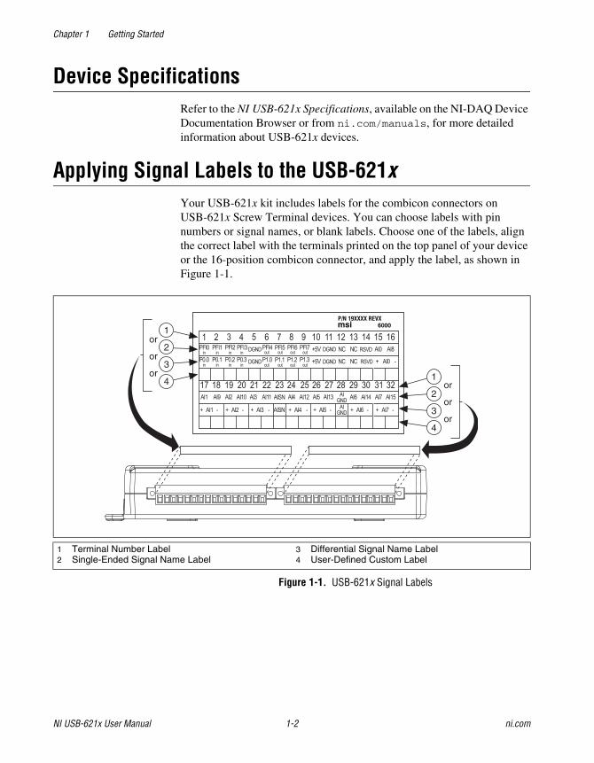
Applying Signal Labels to the USB-621xYour USB-621x kit includes labels for the combicon connectors on USB-621x Screw Terminal devices. You can choose labels with pin numbers or signal names, or blank labels. Choose one of the labels, align the correct label with the terminals printed on the top panel of your device or the 16-position combicon connector, and apply the label, as shown in Figure 1-1.
Figure 1-1. USB-621x Signal Labels
1 Terminal Number Label2 Single-Ended Signal Name Label
3 Differential Signal Name Label4 User-Defined Custom Label
P/N 19XXXX REVXmsi 6000
4
3
2
1or
or
oror
or
or
1
4
3
2
Chapter 1 Getting Started
© National Instruments Corporation 1-3 NI USB-621x User Manual
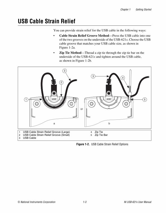
USB Cable Strain ReliefYou can provide strain relief for the USB cable in the following ways:
• Cable Strain Relief Groove Method—Press the USB cable into one of the two grooves on the underside of the USB-621x. Choose the USB cable groove that matches your USB cable size, as shown in Figure 1-2a.
• Zip Tie Method—Thread a zip tie through the zip tie bar on the underside of the USB-621x and tighten around the USB cable, as shown in Figure 1-2b.
Figure 1-2. USB Cable Strain Relief Options
1 USB Cable Strain Relief Groove (Large)2 USB Cable Strain Relief Groove (Small)3 USB Cable
4 Zip Tie5 Zip Tie Bar
1
2
3
3
5
4
a b
or
Chapter 1 Getting Started
NI USB-621x User Manual 1-4 ni.com
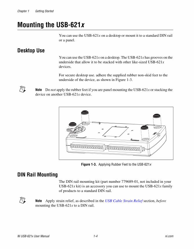
Mounting the USB-621xYou can use the USB-621x on a desktop or mount it to a standard DIN rail or a panel.
Desktop UseYou can use the USB-621x on a desktop. The USB-621x has grooves on the underside that allow it to be stacked with other like-sized USB-621x devices.
For secure desktop use. adhere the supplied rubber non-skid feet to the underside of the device, as shown in Figure 1-3.
Note Do not apply the rubber feet if you are panel mounting the USB-621x or stacking the device on another USB-621x device.
Figure 1-3. Applying Rubber Feet to the USB-621x
DIN Rail MountingThe DIN rail mounting kit (part number 779689-01, not included in your USB-621x kit) is an accessory you can use to mount the USB-621x family of products to a standard DIN rail.
Note Apply strain relief, as described in the USB Cable Strain Relief section, before mounting the USB-621x to a DIN rail.
Chapter 1 Getting Started
© National Instruments Corporation 1-5 NI USB-621x User Manual
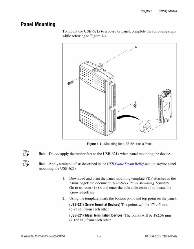
Panel MountingTo mount the USB-621x to a board or panel, complete the following steps while referring to Figure 1-4.
Figure 1-4. Mounting the USB-621x on a Panel
Note Do not apply the rubber feet to the USB-621x when panel mounting the device.
Note Apply strain relief, as described in the USB Cable Strain Relief section, before panel mounting the USB-621x.
1. Download and print the panel mounting template PDF attached in the KnowledgeBase document, USB-621x Panel Mounting Template. Go to ni.com/info and enter the info code ex3x98 to locate the KnowledgeBase.
2. Using the template, mark the bottom point and top point on the panel.
(USB-621x Screw Terminal Devices) The points will be 171.45 mm (6.75 in.) from each other.
(USB-621x Mass Termination Devices) The points will be 182.56 mm (7.188 in.) from each other.
Chapter 1 Getting Started
NI USB-621x User Manual 1-6 ni.com
3. Remove the USB cable from the connector on the USB-621x.
4. Screw a #8 or M4 screw into the bottom point on the panel.
5. Set the USB-621x on the screw by fitting it into the bottom screw notch on the underside of the USB-621x.
6. Screw a #8 or M4 screw through the USB-621x top screw hole into the panel.
© National Instruments Corporation 2-1 NI USB-621x User Manual
2DAQ System Overview
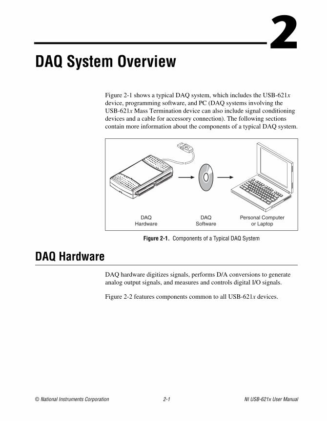
Figure 2-1 shows a typical DAQ system, which includes the USB-621x device, programming software, and PC (DAQ systems involving the USB-621x Mass Termination device can also include signal conditioning devices and a cable for accessory connection). The following sections contain more information about the components of a typical DAQ system.
Figure 2-1. Components of a Typical DAQ System
DAQ HardwareDAQ hardware digitizes signals, performs D/A conversions to generate analog output signals, and measures and controls digital I/O signals.
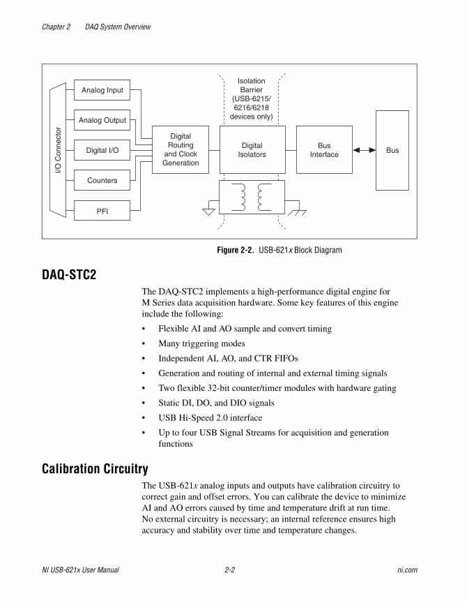
Figure 2-2 features components common to all USB-621x devices.
Personal Computeror Laptop
DAQHardware
DAQSoftware
Chapter 2 DAQ System Overview
NI USB-621x User Manual 2-2 ni.com
Figure 2-2. USB-621x Block Diagram
DAQ-STC2The DAQ-STC2 implements a high-performance digital engine for M Series data acquisition hardware. Some key features of this engine include the following:
• Flexible AI and AO sample and convert timing
• Many triggering modes
• Independent AI, AO, and CTR FIFOs
• Generation and routing of internal and external timing signals
• Two flexible 32-bit counter/timer modules with hardware gating
• Static DI, DO, and DIO signals
• USB Hi-Speed 2.0 interface
• Up to four USB Signal Streams for acquisition and generation functions
Calibration CircuitryThe USB-621x analog inputs and outputs have calibration circuitry to correct gain and offset errors. You can calibrate the device to minimize AI and AO errors caused by time and temperature drift at run time. No external circuitry is necessary; an internal reference ensures high accuracy and stability over time and temperature changes.
Analog Output
Digital I/O
Analog Input
Counters
PFI
DigitalRouting
and ClockGeneration
BusInterface Bus
I/O C
onne
ctor
DigitalIsolators
IsolationBarrier
(USB-6215/6216/6218
devices only)
Chapter 2 DAQ System Overview
© National Instruments Corporation 2-3 NI USB-621x User Manual
Factory-calibration constants are permanently stored in an onboard EEPROM and cannot be modified. When you self-calibrate the device, software stores new constants in a user-modifiable section of the EEPROM. To return a device to its initial factory calibration settings, software can copy the factory-calibration constants to the user-modifiable section of the EEPROM. Refer to the NI-DAQmx Help or the LabVIEW Help in version 8.0 or later for more information about using calibration constants.
For a detailed calibration procedure for USB-621x devices, refer to the B/E/M/S Series Calibration Procedure for NI-DAQmx by clicking Manual Calibration Procedures on ni.com/calibration.
Signal ConditioningMany sensors and transducers require signal conditioning before a measurement system can effectively and accurately acquire the signal. The front-end signal conditioning system can include functions such as signal amplification, attenuation, filtering, electrical isolation, simultaneous sampling, and multiplexing. In addition, many transducers require excitation currents or voltages, bridge completion, linearization, or high amplification for proper and accurate operation. Therefore, most computer-based measurement systems include some form of signal conditioning in addition to plug-in data acquisition DAQ devices.
Sensors and TransducersSensors can generate electrical signals to measure physical phenomena, such as temperature, force, sound, or light. Some commonly used sensors are strain gauges, thermocouples, thermistors, angular encoders, linear encoders, and resistance temperature detectors (RTDs).
To measure signals from these various transducers, you must convert them into a form that a DAQ device can accept. For example, the output voltage of most thermocouples is very small and susceptible to noise. Therefore, you may need to amplify or filter the thermocouple output before digitizing it. The manipulation of signals to prepare them for digitizing is called signal conditioning.
For more information about sensors, refer to the following documents:
• For general information about sensors, visit ni.com/sensors.
• If you are using LabVIEW, refer to the LabVIEW Help by selecting Help»Search the LabVIEW Help in LabVIEW and then navigate to the Taking Measurements book on the Contents tab.
Chapter 2 DAQ System Overview
NI USB-621x User Manual 2-4 ni.com
• If you are using other application software, refer to Common Sensors in the NI-DAQmx Help or the LabVIEW Help in version 8.0 or later.
Cables and AccessoriesCable and accessory options for USB-621x devices are as follows:
• Combicon Accessory for USB-621x Screw Terminal Devices (Optional)—Your USB-621x kit includes combicon connectors with screws and signal labels. The NI USB-621x Accessory Kit (part number 779807-01) contains four additional combicon connectors with screws, a screwdriver, and additional signal labels. You can use the combicon accessory to create custom connection solutions for USB-621x Screw Terminal devices.
• Cables and Accessories for USB-621x Mass Termination Devices—Refer to the USB-6212/6216 Mass Termination Cables and Accessories section of Appendix A, Device-Specific Information, for a list of cables and accessories for USB-621x Mass Termination devices.
USB-621x Mass Termination Custom CablingNI offers cables and accessories for many applications. However, if you want to develop your own cable, adhere to the following guidelines for best results:
• For AI signals, use shielded, twisted-pair wires for each AI pair of differential inputs. Connect the shield for each signal pair to the ground reference at the source.
• Route the analog lines separately from the digital lines.
• When using a cable shield, use separate shields for the analog and digital sections of the cable. Failure to do so results in noise coupling into the analog signals from transient digital signals.
For more information about the connectors used for DAQ devices, refer to the KnowledgeBase document, Specifications and Manufacturers for Board Mating Connectors, by going to ni.com/info and entering the info code rdspmb.
Chapter 2 DAQ System Overview
© National Instruments Corporation 2-5 NI USB-621x User Manual
Programming Devices in SoftwareNational Instruments measurement devices are packaged with NI-DAQ driver software, an extensive library of functions and VIs you can call from your application software, such as LabVIEW or LabWindows/CVI, to program all the features of your NI measurement devices. Driver software has an application programming interface (API), which is a library of VIs, functions, classes, attributes, and properties for creating applications for your device.
USB-621x devices use the NI-DAQmx driver. NI-DAQmx includes a collection of programming examples to help you get started developing an application. You can modify example code and save it in an application. You can use examples to develop a new application or add example code to an existing application.
To locate LabVIEW and LabWindows/CVI examples, open the National Instruments Example Finder.
• In LabVIEW, select Help»Find Examples.
• In LabWindows/CVI, select Help»NI Example Finder.
Measurement Studio, Visual Basic, and ANSI C examples are located in the following directories:
• NI-DAQmx examples for Measurement Studio-supported languages are in the following directories:
– MeasurementStudio\VCNET\Examples\NIDaq
– MeasurementStudio\DotNET\Examples\NIDaq
• NI-DAQmx examples for ANSI C are in the NI-DAQ\Examples\DAQmx ANSI C Dev directory
For additional examples, refer to zone.ni.com.
© National Instruments Corporation 3-1 NI USB-621x User Manual
3Connector and LED Information
The I/O Connector Signal Descriptions and +5 V Power sections contain information about NI USB-621x connectors. The PWR/ACT LED Indicator section contains information about the NI USB-621x PWR/ACT LED. Refer to Appendix A, Device-Specific Information, for device I/O connector pinouts. Refer to the Applying Signal Labels to the USB-621x section of Chapter 1, Getting Started, for information about applying signal labels.
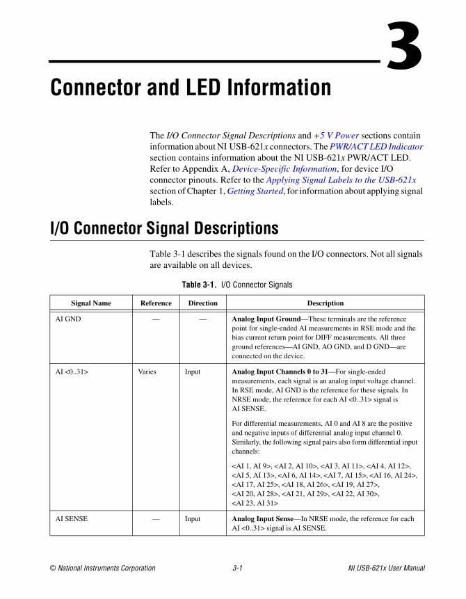
I/O Connector Signal DescriptionsTable 3-1 describes the signals found on the I/O connectors. Not all signals are available on all devices.
Table 3-1. I/O Connector Signals
Signal Name Reference Direction Description
AI GND — — Analog Input Ground—These terminals are the reference point for single-ended AI measurements in RSE mode and the bias current return point for DIFF measurements. All three ground references—AI GND, AO GND, and D GND—are connected on the device.
AI <0..31> Varies Input Analog Input Channels 0 to 31—For single-ended measurements, each signal is an analog input voltage channel. In RSE mode, AI GND is the reference for these signals. In NRSE mode, the reference for each AI <0..31> signal is AI SENSE.
For differential measurements, AI 0 and AI 8 are the positive and negative inputs of differential analog input channel 0. Similarly, the following signal pairs also form differential input channels:
<AI 1, AI 9>, <AI 2, AI 10>, <AI 3, AI 11>, <AI 4, AI 12>, <AI 5, AI 13>, <AI 6, AI 14>, <AI 7, AI 15>, <AI 16, AI 24>, <AI 17, AI 25>, <AI 18, AI 26>, <AI 19, AI 27>, <AI 20, AI 28>, <AI 21, AI 29>, <AI 22, AI 30>, <AI 23, AI 31>
AI SENSE — Input Analog Input Sense—In NRSE mode, the reference for each AI <0..31> signal is AI SENSE.
Chapter 3 Connector and LED Information
© National Instruments Corporation 3-2 NI USB-621x User Manual
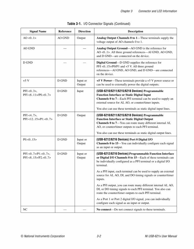
AO <0..1> AO GND Output Analog Output Channels 0 to 1—These terminals supply the voltage output of AO channels 0 to 1.
AO GND — — Analog Output Ground—AO GND is the reference for AO <0..1>. All three ground references—AI GND, AO GND, and D GND—are connected on the device.
D GND — — Digital Ground—D GND supplies the reference for PFI <0..15>/P0/P1 and +5 V. All three ground references—AI GND, AO GND, and D GND—are connected on the device.
+5 V D GND Input or Output
+5 V Power—These terminals provide a +5 V power source or can be used to externally power the digital outputs.
PFI <0..3>, PFI <8..11>/P0.<0..7>
D GND Input (USB-6210/6211/6215/6218 Devices) Programmable Function Interface or Static Digital Input Channels 0 to 7—Each PFI terminal can be used to supply an external source for AI, AO, or counter/timer inputs.
You also can use these terminals as static digital input lines.
PFI <4..7>, PFI <12..15>/P1.<0..7>
D GND Output (USB-6210/6211/6215/6218 Devices) Programmable Function Interface or Static Digital Output Channels 0 to 7—You can route many different internal AI, AO, or counter/timer outputs to each PFI terminal.
You also can use these terminals as static digital output lines.
P0.<0..15> D GND Input or Output
(USB-6212/6216 Devices) Port 0 Digital I/O Channels 0 to 15—You can individually configure each signal as an input or output.
PFI <0..7>/P1.<0..7>, PFI <8..15>/P2.<0..7>
D GND Input or Output
(USB-6212/6216 Devices) Programmable Function Interface or Digital I/O Channels 0 to 15—Each of these terminals can be individually configured as a PFI terminal or a digital I/O terminal.
As a PFI input, each terminal can be used to supply an external source for AI, AO, DI, and DO timing signals or counter/timer inputs.
As a PFI output, you can route many different internal AI, AO, DI, or DO timing signals to each PFI terminal. You also can route the counter/timer outputs to each PFI terminal.
As a Port 1 or Port 2 digital I/O signal, you can individually configure each signal as an input or output.
NC — — No connect—Do not connect signals to these terminals.
Table 3-1. I/O Connector Signals (Continued)
Signal Name Reference Direction Description
Chapter 3 Connector and LED Information
NI USB-621x User Manual 3-3 ni.com
+5 V PowerThe +5 V terminals on the I/O connector can be use as either an output or an input. Both terminals are internally connected on the USB-621x.
+5 V Power as an OutputBecause the USB-621x devices are bus powered, there is a 50 mA limit on the total current that can be drawn from the +5 V terminals and the digital outputs. The USB-621x monitors the total current and drops the voltage on all of the digital outputs and the +5 V terminals if the 50 mA limit is exceeded.
+5 V Power as an InputIf you have high current loads for the digital outputs to drive, you can exceed the 50 mA internal limit by connecting an external +5 V power source to the +5 V terminals. These terminals are protected against undervoltage and overvoltage, and they have a fuse to protect them from short circuit conditions1. If your USB-621x device has more than one +5 V terminal, you can connect the external power supply to one terminal and use the other as a power source.
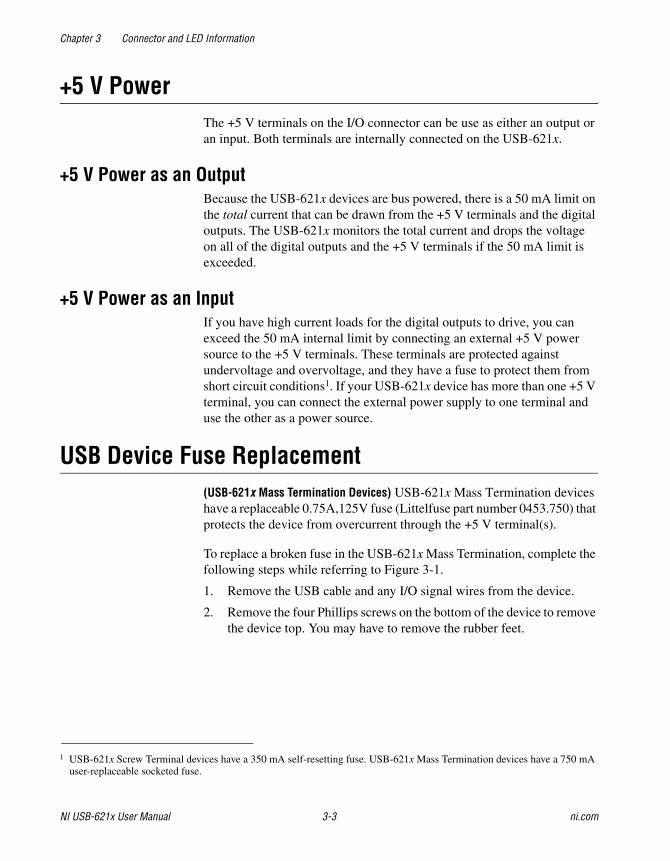
USB Device Fuse Replacement(USB-621x Mass Termination Devices) USB-621x Mass Termination devices have a replaceable 0.75A,125V fuse (Littelfuse part number 0453.750) that protects the device from overcurrent through the +5 V terminal(s).
To replace a broken fuse in the USB-621x Mass Termination, complete the following steps while referring to Figure 3-1.
1. Remove the USB cable and any I/O signal wires from the device.
2. Remove the four Phillips screws on the bottom of the device to remove the device top. You may have to remove the rubber feet.
1 USB-621x Screw Terminal devices have a 350 mA self-resetting fuse. USB-621x Mass Termination devices have a 750 mA user-replaceable socketed fuse.
Chapter 3 Connector and LED Information
© National Instruments Corporation 3-4 NI USB-621x User Manual
3. Replace the broken fuse in the socket. Figure 3-1 shows the fuse location.
Figure 3-1. USB-621x Mass Termination Fuse Location
4. Replace the device top and reattach with the screws.
Note Unscrewing and reinstalling the thread-forming screws over time will produce a compromised connection between the device top and bottom.
1 0.75A,125V Fuse, Socketed
1
NATIONAL
INSTRUMENTS
NI USB-6216
16 Inputs, 16-bit, 400 kS/s,
Isolatoed Multifunction I/O
Chapter 3 Connector and LED Information
NI USB-621x User Manual 3-5 ni.com
PWR/ACT LED IndicatorThe PWR/ACT LED indicator indicates device status. Table 3-2 shows the behavior of the PWR/ACT LED.
Table 3-2. PWR/ACT LED Status
LED State Device Status
Not lit Device not powered or device error. Refer to ni.com/support if device is powered.
On, not blinking Device error. Refer to ni.com/support.
Single-blink Operating normally. Connected to USB Hi-Speed port. Refer to the NI USB-621x Specifications for more information.
Double-blink Connected to USB Full-Speed port. Device performance might be affected. Refer to the NI USB-621x Specifications for more information.
© National Instruments Corporation 4-1 NI USB-621x User Manual
4Analog Input
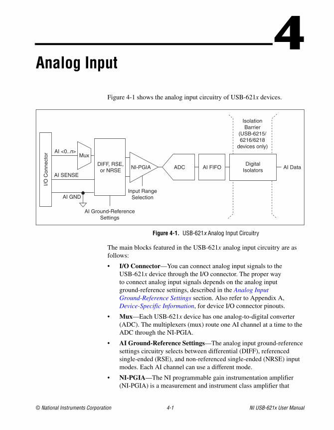
Figure 4-1 shows the analog input circuitry of USB-621x devices.
Figure 4-1. USB-621x Analog Input Circuitry
The main blocks featured in the USB-621x analog input circuitry are as follows:
• I/O Connector—You can connect analog input signals to the USB-621x device through the I/O connector. The proper way to connect analog input signals depends on the analog input ground-reference settings, described in the Analog Input Ground-Reference Settings section. Also refer to Appendix A, Device-Specific Information, for device I/O connector pinouts.
• Mux—Each USB-621x device has one analog-to-digital converter (ADC). The multiplexers (mux) route one AI channel at a time to the ADC through the NI-PGIA.
• AI Ground-Reference Settings—The analog input ground-reference settings circuitry selects between differential (DIFF), referenced single-ended (RSE), and non-referenced single-ended (NRSE) input modes. Each AI channel can use a different mode.
• NI-PGIA—The NI programmable gain instrumentation amplifier (NI-PGIA) is a measurement and instrument class amplifier that
DIFF, RSE,or NRSE
I/O C
onne
ctor
AI <0..n>Mux
AI SENSE
AI GND
NI-PGIA
AI Ground-ReferenceSettings
Input RangeSelection
ADC AI FIFO AI DataDigital
Isolators
IsolationBarrier
(USB-6215/6216/6218
devices only)
Chapter 4 Analog Input
NI USB-621x User Manual 4-2 ni.com
minimizes settling times for all input ranges. The NI-PGIA can amplify or attenuate an AI signal to ensure that you use the maximum resolution of the ADC.
USB-621x devices use the NI-PGIA to deliver high accuracy even when sampling multiple channels with small input ranges at fast rates. USB-621x devices can sample channels in any order at the maximum conversion rate, and you can individually program each channel in a sample with a different input range.
• ADC—The analog-to-digital converter (ADC) digitizes the AI signal by converting the analog voltage into a digital number.
• AI FIFO—USB-621x devices can perform both single and multiple A/D conversions of a fixed or infinite number of samples. A large first-in-first-out (FIFO) buffer holds data during AI acquisitions to ensure that no data is lost. USB-621x devices can handle multiple A/D conversion operations with DMA, interrupts, or programmed I/O.
• Isolation Barrier and Digital Isolators—Refer to Chapter 9, Isolation and Digital Isolators on USB-6215/6216/6218 Devices, for more information.
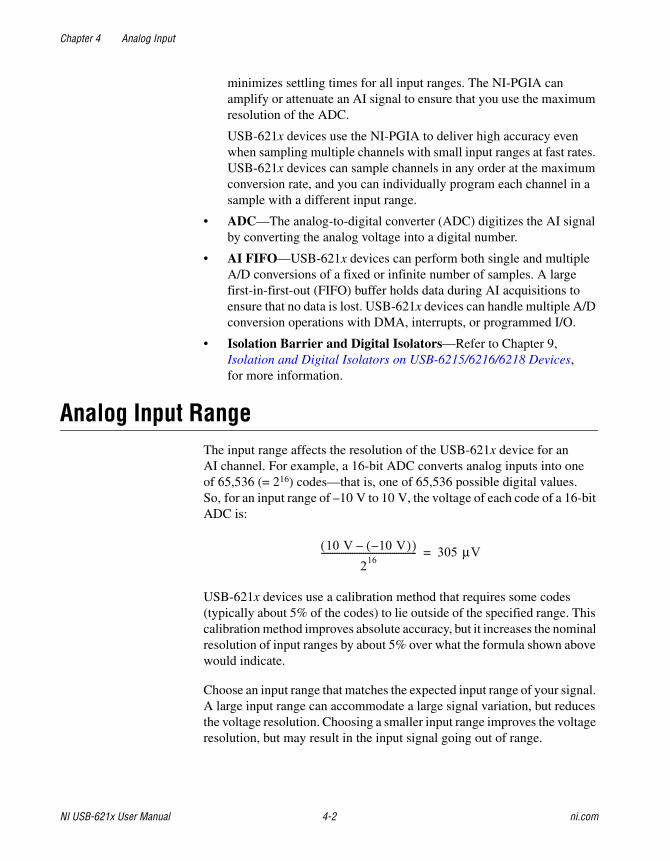
Analog Input RangeThe input range affects the resolution of the USB-621x device for an AI channel. For example, a 16-bit ADC converts analog inputs into one of 65,536 (= 216) codes—that is, one of 65,536 possible digital values. So, for an input range of –10 V to 10 V, the voltage of each code of a 16-bit ADC is:
USB-621x devices use a calibration method that requires some codes (typically about 5% of the codes) to lie outside of the specified range. This calibration method improves absolute accuracy, but it increases the nominal resolution of input ranges by about 5% over what the formula shown above would indicate.
Choose an input range that matches the expected input range of your signal. A large input range can accommodate a large signal variation, but reduces the voltage resolution. Choosing a smaller input range improves the voltage resolution, but may result in the input signal going out of range.
10 V 10 V–( )–( )216
------------------------------------------- 305 μV=
Chapter 4 Analog Input
© National Instruments Corporation 4-3 NI USB-621x User Manual
For more information about setting ranges, refer to the NI-DAQmx Help or the LabVIEW Help in version 8.0 or later.
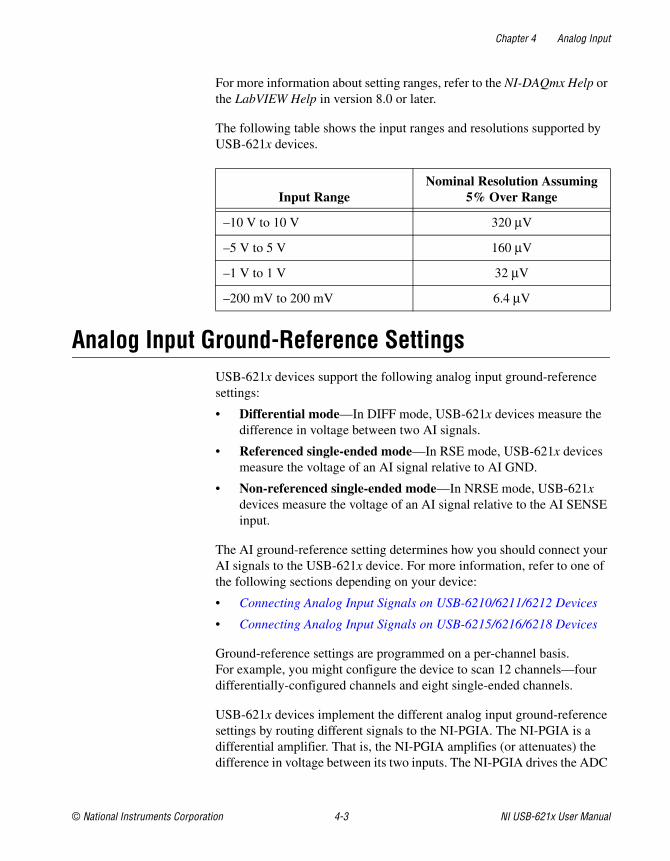
The following table shows the input ranges and resolutions supported by USB-621x devices.
Analog Input Ground-Reference SettingsUSB-621x devices support the following analog input ground-reference settings:
• Differential mode—In DIFF mode, USB-621x devices measure the difference in voltage between two AI signals.
• Referenced single-ended mode—In RSE mode, USB-621x devices measure the voltage of an AI signal relative to AI GND.
• Non-referenced single-ended mode—In NRSE mode, USB-621x devices measure the voltage of an AI signal relative to the AI SENSE input.
The AI ground-reference setting determines how you should connect your AI signals to the USB-621x device. For more information, refer to one of the following sections depending on your device:
• Connecting Analog Input Signals on USB-6210/6211/6212 Devices
• Connecting Analog Input Signals on USB-6215/6216/6218 Devices
Ground-reference settings are programmed on a per-channel basis. For example, you might configure the device to scan 12 channels—four differentially-configured channels and eight single-ended channels.
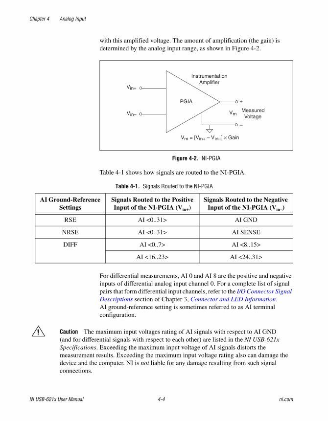
USB-621x devices implement the different analog input ground-reference settings by routing different signals to the NI-PGIA. The NI-PGIA is a differential amplifier. That is, the NI-PGIA amplifies (or attenuates) the difference in voltage between its two inputs. The NI-PGIA drives the ADC
Input RangeNominal Resolution Assuming
5% Over Range
–10 V to 10 V 320 μV
–5 V to 5 V 160 μV
–1 V to 1 V 32 μV
–200 mV to 200 mV 6.4 μV
Chapter 4 Analog Input
NI USB-621x User Manual 4-4 ni.com
with this amplified voltage. The amount of amplification (the gain) is determined by the analog input range, as shown in Figure 4-2.
Figure 4-2. NI-PGIA
Table 4-1 shows how signals are routed to the NI-PGIA.
For differential measurements, AI 0 and AI 8 are the positive and negative inputs of differential analog input channel 0. For a complete list of signal pairs that form differential input channels, refer to the I/O Connector Signal Descriptions section of Chapter 3, Connector and LED Information. AI ground-reference setting is sometimes referred to as AI terminal configuration.
Caution The maximum input voltages rating of AI signals with respect to AI GND (and for differential signals with respect to each other) are listed in the NI USB-621x Specifications. Exceeding the maximum input voltage of AI signals distorts the measurement results. Exceeding the maximum input voltage rating also can damage the device and the computer. NI is not liable for any damage resulting from such signal connections.
Table 4-1. Signals Routed to the NI-PGIA
AI Ground-Reference Settings
Signals Routed to the Positive Input of the NI-PGIA (Vin+)
Signals Routed to the Negative Input of the NI-PGIA (Vin–)
RSE AI <0..31> AI GND
NRSE AI <0..31> AI SENSE
DIFF AI <0..7> AI <8..15>
AI <16..23> AI <24..31>
Vin+
Vm = [Vin+ – Vin–] × Gain
Vm Vin–
PGIA +
–
Measured Voltage
InstrumentationAmplifier
Chapter 4 Analog Input
© National Instruments Corporation 4-5 NI USB-621x User Manual
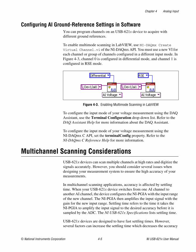
Configuring AI Ground-Reference Settings in SoftwareYou can program channels on an USB-621x device to acquire with different ground references.
To enable multimode scanning in LabVIEW, use NI-DAQmx Create Virtual Channel.vi of the NI-DAQmx API. You must use a new VI for each channel or group of channels configured in a different input mode. In Figure 4-3, channel 0 is configured in differential mode, and channel 1 is configured in RSE mode.
Figure 4-3. Enabling Multimode Scanning in LabVIEW
To configure the input mode of your voltage measurement using the DAQ Assistant, use the Terminal Configuration drop-down list. Refer to the DAQ Assistant Help for more information about the DAQ Assistant.
To configure the input mode of your voltage measurement using the NI-DAQmx C API, set the terminalConfig property. Refer to the NI-DAQmx C Reference Help for more information.
Multichannel Scanning ConsiderationsUSB-621x devices can scan multiple channels at high rates and digitize the signals accurately. However, you should consider several issues when designing your measurement system to ensure the high accuracy of your measurements.
In multichannel scanning applications, accuracy is affected by settling time. When your USB-621x device switches from one AI channel to another AI channel, the device configures the NI-PGIA with the input range of the new channel. The NI-PGIA then amplifies the input signal with the gain for the new input range. Settling time refers to the time it takes the NI-PGIA to amplify the input signal to the desired accuracy before it is sampled by the ADC. The NI USB-621x Specifications lists settling time.
USB-621x devices are designed to have fast settling times. However, several factors can increase the settling time which decreases the accuracy
Chapter 4 Analog Input
NI USB-621x User Manual 4-6 ni.com
of your measurements. To ensure fast settling times, you should do the following (in order of importance):
• Use Low Impedance Sources—To ensure fast settling times, your signal sources should have an impedance of <1 kΩ. Large source impedances increase the settling time of the NI-PGIA, and so decrease the accuracy at fast scanning rates.
Settling times increase when scanning high-impedance signals due to a phenomenon called charge injection. Multiplexers contain switches, usually made of switched capacitors. When one of the channels, for example channel 0, is selected in a multiplexer, those capacitors accumulate charge. When the next channel, for example channel 1, is selected, the accumulated charge leaks backward through channel 1. If the output impedance of the source connected to channel 1 is high enough, the resulting reading of channel 1 can be partially affected by the voltage on channel 0. This effect is referred to as ghosting.
If your source impedance is high, you can decrease the scan rate to allow the NI-PGIA more time to settle. Another option is to use a voltage follower circuit external to your DAQ device to decrease the impedance seen by the DAQ device. Refer to the KnowledgeBase document, How Do I Create a Buffer to Decrease the Source Impedance of My Analog Input Signal?, by going to ni.com/info and entering the info code rdbbis.
• Use Short High-Quality Cabling—Using short high-quality cables can minimize several effects that degrade accuracy including crosstalk, transmission line effects, and noise. The capacitance of the cable also can increase the settling time.
National Instruments recommends using individually shielded, twisted-pair wires that are 2 m or less to connect AI signals to the device. Refer to the Connecting Analog Input Signals on USB-6210/6211/6212 Devices or Connecting Analog Input Signals on USB-6215/6216/6218 Devices section for more information.
• Carefully Choose the Channel Scanning Order
– Avoid Switching from a Large to a Small Input Range—Switching from a channel with a large input range to a channel with a small input range can greatly increase the settling time.
Suppose a 4 V signal is connected to channel 0 and a 1 mV signal is connected to channel 1. The input range for channel 0 is –10 V to 10 V and the input range of channel 1 is –200 mV to 200 mV.
When the multiplexer switches from channel 0 to channel 1, the input to the NI-PGIA switches from 4 V to 1 mV. The
Chapter 4 Analog Input
© National Instruments Corporation 4-7 NI USB-621x User Manual
approximately 4 V step from 4 V to 1 mV is 1,000% of the new full-scale range. For a 16-bit device to settle within 0.0015% (15 ppm or 1 LSB) of the ±200 mV full-scale range on channel 1, the input circuitry must settle to within 0.000031% (0.31 ppm or 1/50 LSB) of the ±10 V range. Some devices can take many microseconds for the circuitry to settle this much.
To avoid this effect, you should arrange your channel scanning order so that transitions from large to small input ranges are infrequent.
In general, you do not need this extra settling time when the NI-PGIA is switching from a small input range to a larger input range.
– Insert Grounded Channel between Signal Channels—Another technique to improve settling time is to connect an input channel to ground. Then insert this channel in the scan list between two of your signal channels. The input range of the grounded channel should match the input range of the signal after the grounded channel in the scan list.
Consider again the example above where a 4 V signal is connected to channel 0 and a 1 mV signal is connected to channel 1. Suppose the input range for channel 0 is –10 V to 10 V and the input range of channel 1 is –200 mV to 200 mV.
You can connect channel 2 to AI GND (or you can use the internal ground signal; refer to Internal Channels in the NI-DAQmx Help). Set the input range of channel 2 to –200 mV to 200 mV to match channel 1. Then scan channels in the order: 0, 2, 1.
Inserting a grounded channel between signal channels improves settling time because the NI-PGIA adjusts to the new input range setting faster when the input is grounded.
– Minimize Voltage Step between Adjacent Channels—When scanning between channels that have the same input range, the settling time increases with the voltage step between the channels. If you know the expected input range of your signals, you can group signals with similar expected ranges together in your scan list.
For example, suppose all channels in a system use a –5 to 5 V input range. The signals on channels 0, 2, and 4 vary between 4.3 V and 5 V. The signals on channels 1, 3, and 5 vary between –4 V and 0 V. Scanning channels in the order 0, 2, 4, 1, 3, 5 produces more accurate results than scanning channels in the order 0, 1, 2, 3, 4, 5.
Chapter 4 Analog Input
NI USB-621x User Manual 4-8 ni.com
• Avoid Scanning Faster Than Necessary—Designing your system to scan at slower speeds gives the NI-PGIA more time to settle to a more accurate level. Consider the following examples:
– Example 1—Averaging many AI samples can increase the accuracy of the reading by decreasing noise effects. In general, the more points you average, the more accurate the final result. However, you may choose to decrease the number of points you average and slow down the scanning rate.
Suppose you want to sample 10 channels over a period of 20 ms and average the results. You could acquire 250 points from each channel at a scan rate of 125 kS/s. Another method would be to acquire 500 points from each channel at a scan rate of 250 kS/s. Both methods take the same amount of time. Doubling the number of samples averaged (from 250 to 500) decreases the effect of noise by a factor of 1.4 (the square root of 2). However, doubling the number of samples (in this example) decreases the time the NI-PGIA has to settle from 8 μs to 4 μs. In some cases, the slower scan rate system returns more accurate results.
– Example 2—If the time relationship between channels is not critical, you can sample from the same channel multiple times and scan less frequently. For example, suppose an application requires averaging 100 points from channel 0 and averaging 100 points from channel 1. You could alternate reading between channels—that is, read one point from channel 0, then one point from channel 1, and so on. You also could read all 100 points from channel 0 then read 100 points from channel 1. The second method switches between channels much often and is affected less by settling time.
Analog Input Data Acquisition MethodsWhen performing analog input measurements, you either can perform software-timed or hardware-timed acquisitions:
• Software-Timed Acquisitions—With a software-timed acquisition, software controls the rate of the acquisition. Software sends a separate command to the hardware to initiate each ADC conversion. In NI-DAQmx, software-timed acquisitions are referred to as having on-demand timing. Software-timed acquisitions are also referred to as immediate or static acquisitions and are typically used for reading a single sample of data.
Chapter 4 Analog Input
© National Instruments Corporation 4-9 NI USB-621x User Manual
• Hardware-Timed Acquisitions—With hardware-timed acquisitions, a digital hardware signal, AI Sample Clock, controls the rate of the acquisition. This signal can be generated internally on your device or provided externally.
Hardware-timed acquisitions have several advantages over software-timed acquisitions:
– The time between samples can be much shorter.
– The timing between samples is deterministic.
– Hardware-timed acquisitions can use hardware triggering.
Hardware-timed operations are buffered. In a buffered acquisition, data is moved from the DAQ device’s onboard FIFO memory to a PC buffer using USB signal streams or programmed I/O before it is transferred to application memory. Buffered acquisitions typically allow for much faster transfer rates than non-buffered acquisitions because data is moved in large blocks, rather than one point at a time.
One property of buffered I/O operations is the sample mode. The sample mode can be either finite or continuous.
Finite sample mode acquisition refers to the acquisition of a specific, predetermined number of data samples. After the specified number of samples has been read in, the acquisition stops. If you use a reference trigger, you must use finite sample mode.
Continuous acquisition refers to the acquisition of an unspecified number of samples. Instead of acquiring a set number of data samples and stopping, a continuous acquisition continues until you stop the operation. Continuous acquisition is also referred to as double-buffered or circular-buffered acquisition.
If data cannot be transferred across the bus fast enough, the FIFO becomes full. New acquisitions will overwrite data in the FIFO before it can be transferred to host memory. The device generates an error in this case. With continuous operations, if the user program does not read data out of the PC buffer fast enough to keep up with the data transfer, the buffer could reach an overflow condition, causing an error to be generated.
Chapter 4 Analog Input
NI USB-621x User Manual 4-10 ni.com
Analog Input Digital TriggeringAnalog input supports three different triggering actions:
• Start trigger
• Reference trigger
• Pause trigger
Refer to the AI Start Trigger Signal, AI Reference Trigger Signal, and AI Pause Trigger Signal sections for information about these triggers.
A digital trigger can initiate these actions. All USB-621x devices support digital triggering. USB-621x devices do not support analog triggering.
Field Wiring ConsiderationsEnvironmental noise can seriously affect the measurement accuracy of the device if you do not take proper care when running signal wires between signal sources and the device. The following recommendations apply mainly to AI signal routing to the device, although they also apply to signal routing in general.
Minimize noise pickup and maximize measurement accuracy by taking the following precautions:
• Use DIFF AI connections to reject common-mode noise.
• Use individually shielded, twisted-pair wires to connect AI signals to the device. With this type of wire, the signals attached to the positive and negative input channels are twisted together and then covered with a shield. You then connect this shield only at one point to the signal source ground. This kind of connection is required for signals traveling through areas with large magnetic fields or high electromagnetic interference.
Refer to the NI Developer Zone document, Field Wiring and Noise Considerations for Analog Signals, for more information. To access this document, go to ni.com/info and enter the info code rdfwn3.
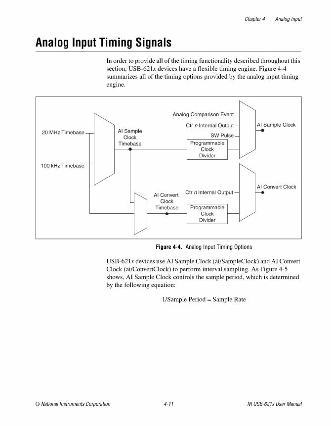
Chapter 4 Analog Input
© National Instruments Corporation 4-11 NI USB-621x User Manual
Analog Input Timing SignalsIn order to provide all of the timing functionality described throughout this section, USB-621x devices have a flexible timing engine. Figure 4-4 summarizes all of the timing options provided by the analog input timing engine.
Figure 4-4. Analog Input Timing Options
USB-621x devices use AI Sample Clock (ai/SampleClock) and AI Convert Clock (ai/ConvertClock) to perform interval sampling. As Figure 4-5 shows, AI Sample Clock controls the sample period, which is determined by the following equation:
1/Sample Period = Sample Rate
20 MHz Timebase
100 kHz Timebase
ProgrammableClock
Divider
ProgrammableClock
Divider
AI SampleClock
Timebase
AI Convert Clock
Timebase
Analog Comparison Event
Ctr n Internal Output
SW Pulse
Ctr n Internal OutputAI Convert Clock
AI Sample Clock
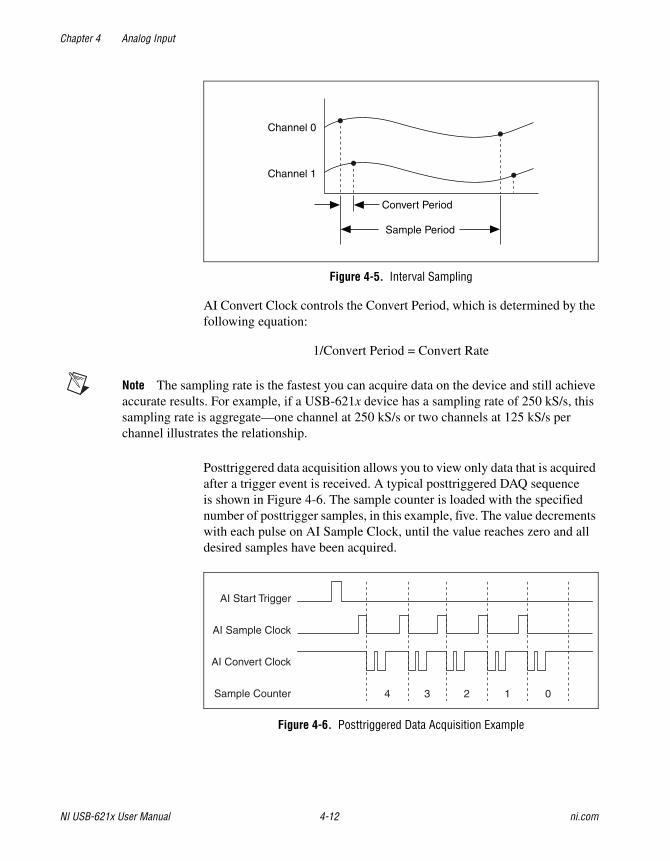
Chapter 4 Analog Input
NI USB-621x User Manual 4-12 ni.com
Figure 4-5. Interval Sampling
AI Convert Clock controls the Convert Period, which is determined by the following equation:
1/Convert Period = Convert Rate
Note The sampling rate is the fastest you can acquire data on the device and still achieve accurate results. For example, if a USB-621x device has a sampling rate of 250 kS/s, this sampling rate is aggregate—one channel at 250 kS/s or two channels at 125 kS/s per channel illustrates the relationship.
Posttriggered data acquisition allows you to view only data that is acquired after a trigger event is received. A typical posttriggered DAQ sequence is shown in Figure 4-6. The sample counter is loaded with the specified number of posttrigger samples, in this example, five. The value decrements with each pulse on AI Sample Clock, until the value reaches zero and all desired samples have been acquired.
Figure 4-6. Posttriggered Data Acquisition Example
Channel 0
Channel 1
Convert Period
Sample Period
1 3 0 4 2
AI Start Trigger
AI Sample Clock
AI Convert Clock
Sample Counter
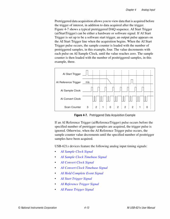
Chapter 4 Analog Input
© National Instruments Corporation 4-13 NI USB-621x User Manual
Pretriggered data acquisition allows you to view data that is acquired before the trigger of interest, in addition to data acquired after the trigger. Figure 4-7 shows a typical pretriggered DAQ sequence. AI Start Trigger (ai/StartTrigger) can be either a hardware or software signal. If AI Start Trigger is set up to be a software start trigger, an output pulse appears on the AI Start Trigger line when the acquisition begins. When the AI Start Trigger pulse occurs, the sample counter is loaded with the number of pretriggered samples, in this example, four. The value decrements with each pulse on AI Sample Clock, until the value reaches zero. The sample counter is then loaded with the number of posttriggered samples, in this example, three.
Figure 4-7. Pretriggered Data Acquisition Example
If an AI Reference Trigger (ai/ReferenceTrigger) pulse occurs before the specified number of pretrigger samples are acquired, the trigger pulse is ignored. Otherwise, when the AI Reference Trigger pulse occurs, the sample counter value decrements until the specified number of posttrigger samples have been acquired.
USB-621x devices feature the following analog input timing signals:
• AI Sample Clock Signal
• AI Sample Clock Timebase Signal
• AI Convert Clock Signal
• AI Convert Clock Timebase Signal
• AI Hold Complete Event Signal
• AI Start Trigger Signal
• AI Reference Trigger Signal
• AI Pause Trigger Signal
n/a
0 1 2 3 1 0 2 2 2
AI Start Trigger
AI Reference Trigger
AI Sample Clock
AI Convert Clock
Scan Counter
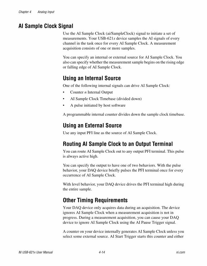
Chapter 4 Analog Input
NI USB-621x User Manual 4-14 ni.com
AI Sample Clock SignalUse the AI Sample Clock (ai/SampleClock) signal to initiate a set of measurements. Your USB-621x device samples the AI signals of every channel in the task once for every AI Sample Clock. A measurement acquisition consists of one or more samples.
You can specify an internal or external source for AI Sample Clock. You also can specify whether the measurement sample begins on the rising edge or falling edge of AI Sample Clock.
Using an Internal SourceOne of the following internal signals can drive AI Sample Clock:
• Counter n Internal Output
• AI Sample Clock Timebase (divided down)
• A pulse initiated by host software
A programmable internal counter divides down the sample clock timebase.
Using an External SourceUse any input PFI line as the source of AI Sample Clock.
Routing AI Sample Clock to an Output TerminalYou can route AI Sample Clock out to any output PFI terminal. This pulse is always active high.
You can specify the output to have one of two behaviors. With the pulse behavior, your DAQ device briefly pulses the PFI terminal once for every occurrence of AI Sample Clock.
With level behavior, your DAQ device drives the PFI terminal high during the entire sample.
Other Timing RequirementsYour DAQ device only acquires data during an acquisition. The device ignores AI Sample Clock when a measurement acquisition is not in progress. During a measurement acquisition, you can cause your DAQ device to ignore AI Sample Clock using the AI Pause Trigger signal.
A counter on your device internally generates AI Sample Clock unless you select some external source. AI Start Trigger starts this counter and either
Chapter 4 Analog Input
© National Instruments Corporation 4-15 NI USB-621x User Manual
software or hardware can stop it once a finite acquisition completes. When using an internally generated AI Sample Clock, you also can specify a configurable delay from AI Start Trigger to the first AI Sample Clock pulse. By default, this delay is set to two ticks of the AI Sample Clock Timebase signal. When using an externally generated AI Sample Clock, you must ensure the clock signal is consistent with respect to the timing requirements of AI Convert Clock. Failure to do so may result in AI Sample Clock pulses that are masked off and acquisitions with erratic sampling intervals. Refer to the AI Convert Clock Signal section for more information about the timing requirements between AI Convert Clock and AI Sample Clock.
Figure 4-8 shows the relationship of AI Sample Clock to AI Start Trigger.
Figure 4-8. AI Sample Clock and AI Start Trigger
AI Sample Clock Timebase SignalYou can route any of the following signals to be the AI Sample Clock Timebase (ai/SampleClockTimebase) signal:
• 20 MHz Timebase
• 100 kHz Timebase
• (USB-6210/6211/6215 Devices) PFI <0..3>
• (USB-6212/6216 Devices) PFI <0..15>
• (USB-6218 Devices) PFI <0..3>, PFI <8..11>
AI Sample Clock Timebase is not available as an output on the I/O connector. AI Sample Clock Timebase is divided down to provide one of the possible sources for AI Sample Clock. You can configure the polarity selection for AI Sample Clock Timebase as either rising or falling edge.
AI Sample Clock Timebase
AI Start Trigger
AI Sample Clock
Delay From Start
Trigger
Chapter 4 Analog Input
NI USB-621x User Manual 4-16 ni.com
AI Convert Clock SignalUse the AI Convert Clock (ai/ConvertClock) signal to initiate a single A/D conversion on a single channel. A sample (controlled by the AI Sample Clock) consists of one or more conversions.
You can specify either an internal or external signal as the source of AI Convert Clock. You also can specify whether the measurement sample begins on the rising edge or falling edge of AI Convert Clock.
By default, NI-DAQmx chooses the fastest conversion rate possible based on the speed of the A/D converter and adds 10 μs of padding between each channel to allow for adequate settling time. This scheme enables the channels to approximate simultaneous sampling and still allow for adequate settling time. If the AI Sample Clock rate is too fast to allow for this 10 μs of padding, NI-DAQmx chooses the conversion rate so that the AI Convert Clock pulses are evenly spaced throughout the sample.
To explicitly specify the conversion rate, use AI Convert Clock Rate DAQmx Timing property node or function.
Caution Setting the conversion rate higher than the maximum rate specified for your device will result in errors.
Using an Internal SourceOne of the following internal signals can drive AI Convert Clock:
• AI Convert Clock Timebase (divided down)
• Counter n Internal Output
A programmable internal counter divides down the AI Convert Clock Timebase to generate AI Convert Clock. Started by AI Sample Clock, the counter counts down to zero, produces an AI Convert Clock, reloads itself, and repeats the process until the sample is finished. It then reloads itself in preparation for the next AI Sample Clock pulse.
Using an External SourceUse any input PFI line as the source of AI Convert Clock.
Routing AI Convert Clock to an Output TerminalYou can route AI Convert Clock (as an active low signal) out to any output PFI terminal.
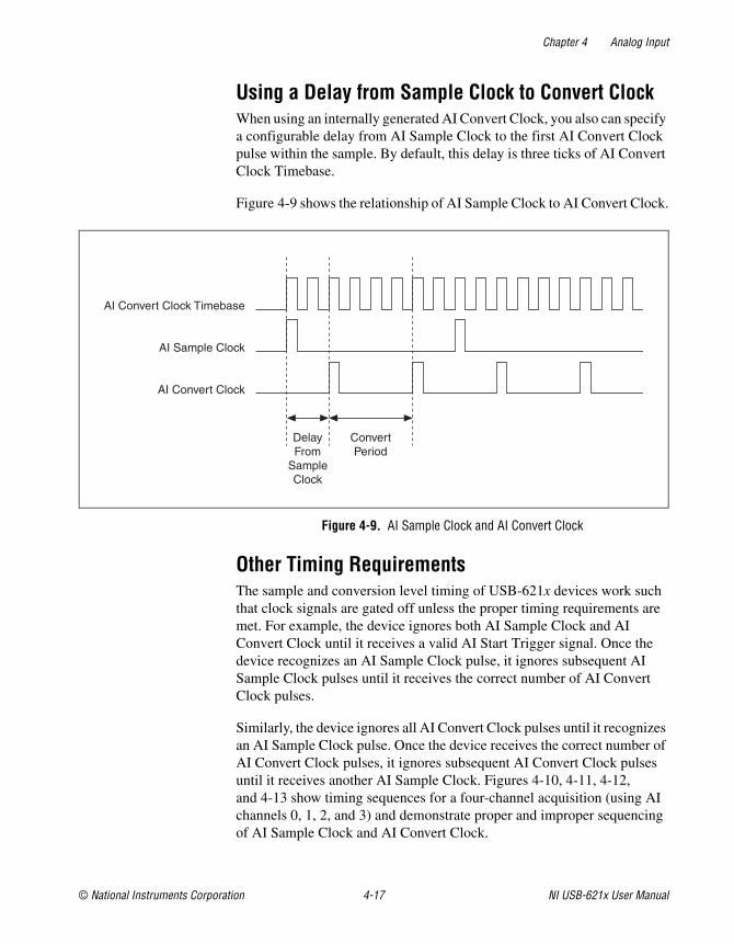
Chapter 4 Analog Input
© National Instruments Corporation 4-17 NI USB-621x User Manual
Using a Delay from Sample Clock to Convert ClockWhen using an internally generated AI Convert Clock, you also can specify a configurable delay from AI Sample Clock to the first AI Convert Clock pulse within the sample. By default, this delay is three ticks of AI Convert Clock Timebase.
Figure 4-9 shows the relationship of AI Sample Clock to AI Convert Clock.
Figure 4-9. AI Sample Clock and AI Convert Clock
Other Timing RequirementsThe sample and conversion level timing of USB-621x devices work such that clock signals are gated off unless the proper timing requirements are met. For example, the device ignores both AI Sample Clock and AI Convert Clock until it receives a valid AI Start Trigger signal. Once the device recognizes an AI Sample Clock pulse, it ignores subsequent AI Sample Clock pulses until it receives the correct number of AI Convert Clock pulses.
Similarly, the device ignores all AI Convert Clock pulses until it recognizes an AI Sample Clock pulse. Once the device receives the correct number of AI Convert Clock pulses, it ignores subsequent AI Convert Clock pulses until it receives another AI Sample Clock. Figures 4-10, 4-11, 4-12, and 4-13 show timing sequences for a four-channel acquisition (using AI channels 0, 1, 2, and 3) and demonstrate proper and improper sequencing of AI Sample Clock and AI Convert Clock.
AI Convert Clock Timebase
AI Sample Clock
AI Convert Clock
Delay From
Sample Clock
Convert Period
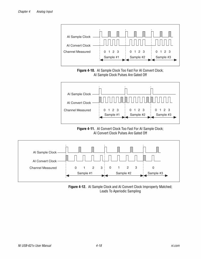
Chapter 4 Analog Input
NI USB-621x User Manual 4-18 ni.com
Figure 4-10. AI Sample Clock Too Fast For AI Convert Clock; AI Sample Clock Pulses Are Gated Off
Figure 4-11. AI Convert Clock Too Fast For AI Sample Clock; AI Convert Clock Pulses Are Gated Off
Figure 4-12. AI Sample Clock and AI Convert Clock Improperly Matched; Leads To Aperiodic Sampling
AI Sample Clock
AI Convert Clock
Sample #1 Sample #2 Sample #3
Channel Measured 1 2 3 0 1 2 3 0 1 2 3 0
AI Sample Clock
AI Convert Clock
Sample #1 Sample #2 Sample #3
1 2 3 0 1 2 3 0 1 2 3 0 Channel Measured
AI Sample Clock
AI Convert Clock
Sample #1 Sample #2 Sample #3
1 2 3 0 0 Channel Measured 1 2 3 0
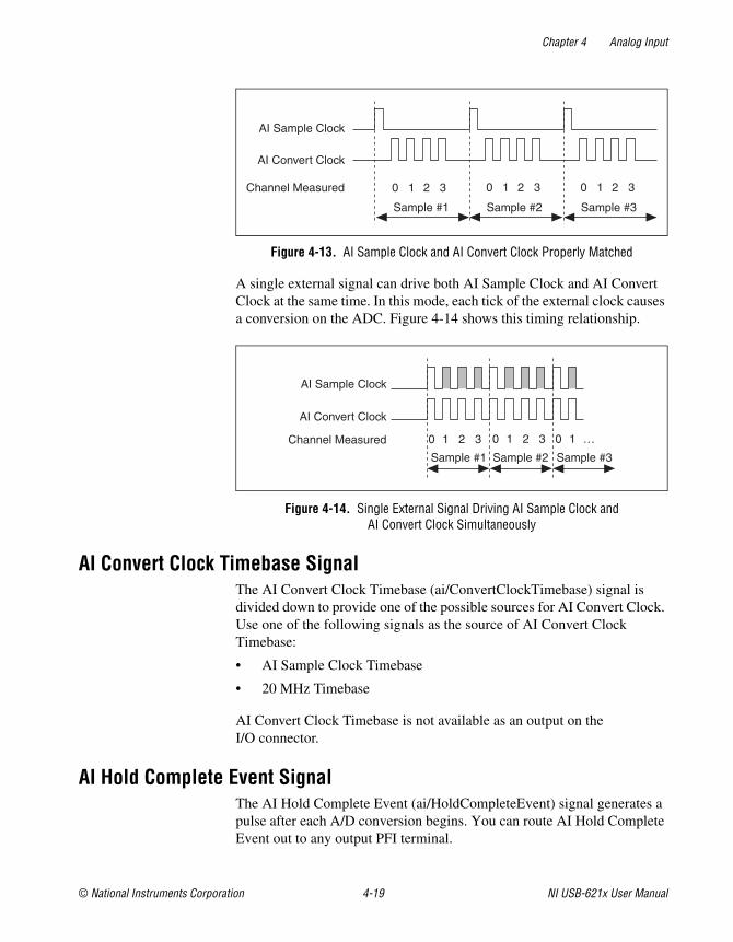
Chapter 4 Analog Input
© National Instruments Corporation 4-19 NI USB-621x User Manual
Figure 4-13. AI Sample Clock and AI Convert Clock Properly Matched
A single external signal can drive both AI Sample Clock and AI Convert Clock at the same time. In this mode, each tick of the external clock causes a conversion on the ADC. Figure 4-14 shows this timing relationship.
Figure 4-14. Single External Signal Driving AI Sample Clock and AI Convert Clock Simultaneously
AI Convert Clock Timebase SignalThe AI Convert Clock Timebase (ai/ConvertClockTimebase) signal is divided down to provide one of the possible sources for AI Convert Clock. Use one of the following signals as the source of AI Convert Clock Timebase:
• AI Sample Clock Timebase
• 20 MHz Timebase
AI Convert Clock Timebase is not available as an output on the I/O connector.
AI Hold Complete Event SignalThe AI Hold Complete Event (ai/HoldCompleteEvent) signal generates a pulse after each A/D conversion begins. You can route AI Hold Complete Event out to any output PFI terminal.
AI Sample Clock
AI Convert Clock
Sample #1 Sample #2 Sample #3
Channel Measured 1 2 3 0 1 2 3 0 1 2 3 0
AI Sample Clock
AI Convert Clock
Sample #1 Sample #2 Sample #3
1 2 3 0 1 2 3 0 1 … 0 Channel Measured
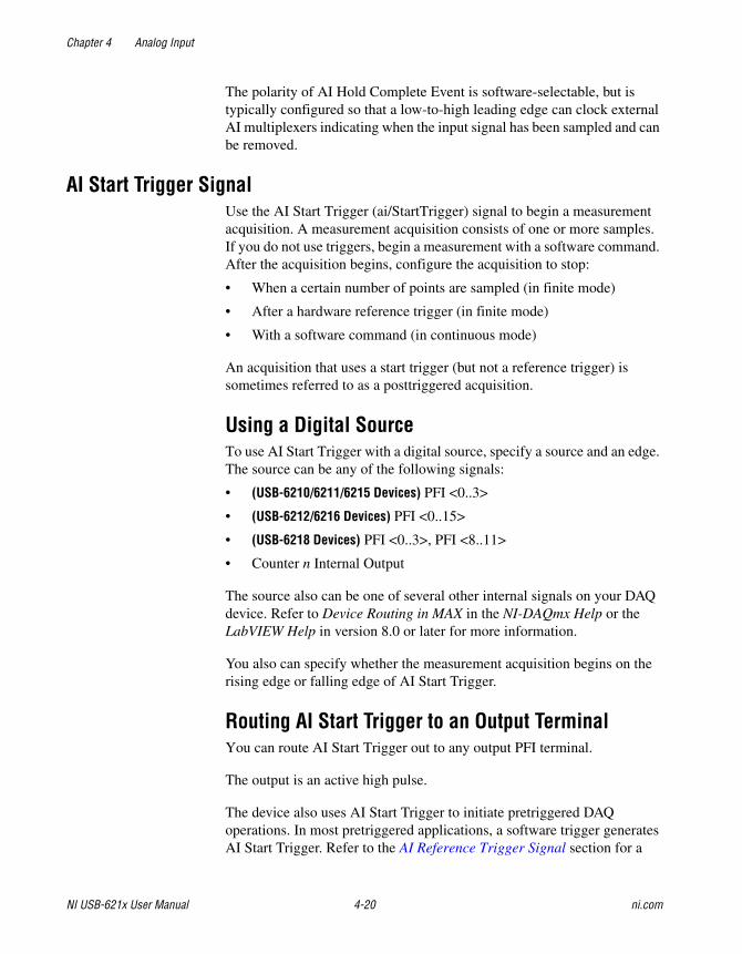
Chapter 4 Analog Input
NI USB-621x User Manual 4-20 ni.com
The polarity of AI Hold Complete Event is software-selectable, but is typically configured so that a low-to-high leading edge can clock external AI multiplexers indicating when the input signal has been sampled and can be removed.
AI Start Trigger SignalUse the AI Start Trigger (ai/StartTrigger) signal to begin a measurement acquisition. A measurement acquisition consists of one or more samples. If you do not use triggers, begin a measurement with a software command. After the acquisition begins, configure the acquisition to stop:
• When a certain number of points are sampled (in finite mode)
• After a hardware reference trigger (in finite mode)
• With a software command (in continuous mode)
An acquisition that uses a start trigger (but not a reference trigger) is sometimes referred to as a posttriggered acquisition.
Using a Digital SourceTo use AI Start Trigger with a digital source, specify a source and an edge. The source can be any of the following signals:
• (USB-6210/6211/6215 Devices) PFI <0..3>
• (USB-6212/6216 Devices) PFI <0..15>
• (USB-6218 Devices) PFI <0..3>, PFI <8..11>
• Counter n Internal Output
The source also can be one of several other internal signals on your DAQ device. Refer to Device Routing in MAX in the NI-DAQmx Help or the LabVIEW Help in version 8.0 or later for more information.
You also can specify whether the measurement acquisition begins on the rising edge or falling edge of AI Start Trigger.
Routing AI Start Trigger to an Output TerminalYou can route AI Start Trigger out to any output PFI terminal.
The output is an active high pulse.
The device also uses AI Start Trigger to initiate pretriggered DAQ operations. In most pretriggered applications, a software trigger generates AI Start Trigger. Refer to the AI Reference Trigger Signal section for a
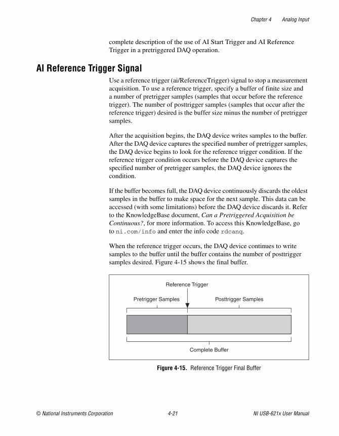
Chapter 4 Analog Input
© National Instruments Corporation 4-21 NI USB-621x User Manual
complete description of the use of AI Start Trigger and AI Reference Trigger in a pretriggered DAQ operation.
AI Reference Trigger SignalUse a reference trigger (ai/ReferenceTrigger) signal to stop a measurement acquisition. To use a reference trigger, specify a buffer of finite size and a number of pretrigger samples (samples that occur before the reference trigger). The number of posttrigger samples (samples that occur after the reference trigger) desired is the buffer size minus the number of pretrigger samples.
After the acquisition begins, the DAQ device writes samples to the buffer. After the DAQ device captures the specified number of pretrigger samples, the DAQ device begins to look for the reference trigger condition. If the reference trigger condition occurs before the DAQ device captures the specified number of pretrigger samples, the DAQ device ignores the condition.
If the buffer becomes full, the DAQ device continuously discards the oldest samples in the buffer to make space for the next sample. This data can be accessed (with some limitations) before the DAQ device discards it. Refer to the KnowledgeBase document, Can a Pretriggered Acquisition be Continuous?, for more information. To access this KnowledgeBase, go to ni.com/info and enter the info code rdcanq.
When the reference trigger occurs, the DAQ device continues to write samples to the buffer until the buffer contains the number of posttrigger samples desired. Figure 4-15 shows the final buffer.
Figure 4-15. Reference Trigger Final Buffer
Reference Trigger
Pretrigger Samples
Complete Buffer
Posttrigger Samples
Chapter 4 Analog Input
NI USB-621x User Manual 4-22 ni.com
Using a Digital SourceTo use AI Reference Trigger with a digital source, specify a source and an edge. The source can be any input PFI signal.
The source also can be one of several internal signals on your DAQ device. Refer to Device Routing in MAX in the NI-DAQmx Help or the LabVIEW Help in version 8.0 or later for more information.
You also can specify whether the measurement acquisition stops on the rising edge or falling edge of AI Reference Trigger.
Routing AI Reference Trigger to an Output TerminalYou can route AI Reference Trigger out to any output PFI terminal.
AI Pause Trigger SignalYou can use the AI Pause Trigger (ai/PauseTrigger) signal to pause and resume a measurement acquisition. The internal sample clock pauses while the external trigger signal is active and resumes when the signal is inactive. You can program the active level of the pause trigger to be high or low.
Using a Digital SourceTo use AI Sample Clock, specify a source and a polarity. The source can be any input PFI signal.
The source also can be one of several other internal signals on your DAQ device. Refer to Device Routing in MAX in the NI-DAQmx Help or the LabVIEW Help in version 8.0 or later for more information.
Getting Started with AI Applications in SoftwareYou can use the USB-621x device in the following analog input applications:
• Single-point analog input
• Finite analog input
• Continuous analog input
You can perform these applications through DMA, interrupt, or programmed I/O data transfer mechanisms. Some of the applications also use start, reference, and pause triggers.
Chapter 4 Analog Input
© National Instruments Corporation 4-23 NI USB-621x User Manual
Note For more information about programming analog input applications and triggers in software, refer to the NI-DAQmx Help or the LabVIEW Help in version 8.0 or later.
Connecting Analog Input Signals on USB-6210/6211/6212 Devices
Table 4-2 summarizes the recommended input configuration for both types of signal sources on USB-6210/6211/6212 devices.
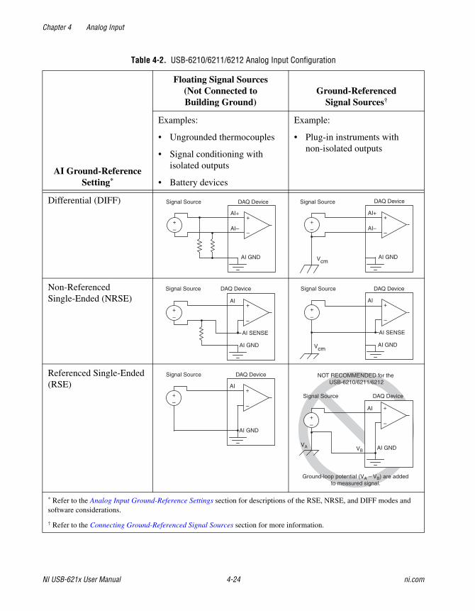
Chapter 4 Analog Input
NI USB-621x User Manual 4-24 ni.com
Table 4-2. USB-6210/6211/6212 Analog Input Configuration
AI Ground-Reference Setting*
Floating Signal Sources (Not Connected to Building Ground)
Ground-Referenced Signal Sources†
Examples:
• Ungrounded thermocouples
• Signal conditioning with isolated outputs
• Battery devices
Example:
• Plug-in instruments with non-isolated outputs
Differential (DIFF)
Non-Referenced Single-Ended (NRSE)
Referenced Single-Ended (RSE)
* Refer to the Analog Input Ground-Reference Settings section for descriptions of the RSE, NRSE, and DIFF modes and software considerations.
† Refer to the Connecting Ground-Referenced Signal Sources section for more information.
+ –
+
–
AI+
AI–
AI GND
Signal Source DAQ Device
+–
+
–
AI+
AI–
AI GND
Signal Source DAQ Device
Vcm
+–
+
–
AI
AI SENSE
AI GND
Signal Source DAQ Device
+–
+
–
AI
AI SENSE
AI GND
Signal Source DAQ Device
Vcm
+–
+
–
AI
AI GND
Signal Source DAQ Device
Ground-loop potential (VA – VB) are addedto measured signal.
NOT RECOMMENDED for the USB-6210/6211/6212
+–
+
–
AI
AI GNDVBVA
DAQ DeviceSignal Source
Chapter 4 Analog Input
© National Instruments Corporation 4-25 NI USB-621x User Manual
Connecting Floating Signal Sources
What Are Floating Signal Sources?A floating signal source is not connected to the building ground system, but has an isolated ground-reference point. Some examples of floating signal sources are outputs of transformers, thermocouples, battery-powered devices, optical isolators, and isolation amplifiers. An instrument or device that has an isolated output is a floating signal source.
When to Use Differential Connections with Floating Signal SourcesUse DIFF input connections for any channel that meets any of the following conditions:
• The input signal is low level (less than 1 V).
• The leads connecting the signal to the device are greater than 3 m (10 ft).
• The input signal requires a separate ground-reference point or return signal.
• The signal leads travel through noisy environments.
• Two analog input channels, AI+ and AI–, are available for the signal.
DIFF signal connections reduce noise pickup and increase common-mode noise rejection. DIFF signal connections also allow input signals to float within the common-mode limits of the NI-PGIA.
Refer to the Using Differential Connections for Floating Signal Sources section for more information about differential connections.
When to Use Referenced Single-Ended (RSE) Connections with Floating Signal SourcesOnly use RSE input connections if the input signal meets the following conditions:
• The input signal can share a common reference point, AI GND, with other signals that use RSE.
• The input signal is high-level (greater than 1 V).
• The leads connecting the signal to the device are less than 3 m (10 ft).
Chapter 4 Analog Input
NI USB-621x User Manual 4-26 ni.com
DIFF input connections are recommended for greater signal integrity for any input signal that does not meet the preceding conditions.
In the single-ended modes, more electrostatic and magnetic noise couples into the signal connections than in DIFF configurations. The coupling is the result of differences in the signal path. Magnetic coupling is proportional to the area between the two signal conductors. Electrical coupling is a function of how much the electric field differs between the two conductors.
With this type of connection, the NI-PGIA rejects both the common-mode noise in the signal and the ground potential difference between the signal source and the device ground.
Refer to the Using Referenced Single-Ended (RSE) Connections for Floating Signal Sources section for more information about RSE connections.
When to Use Non-Referenced Single-Ended (NRSE) Connections with Floating Signal SourcesOnly use NRSE input connections if the input signal meets the following conditions:
• The input signal is high-level (greater than 1 V).
• The leads connecting the signal to the device are less than 3 m (10 ft).
DIFF input connections are recommended for greater signal integrity for any input signal that does not meet the preceding conditions.
In the single-ended modes, more electrostatic and magnetic noise couples into the signal connections than in DIFF configurations. The coupling is the result of differences in the signal path. Magnetic coupling is proportional to the area between the two signal conductors. Electrical coupling is a function of how much the electric field differs between the two conductors.
With this type of connection, the NI-PGIA rejects both the common-mode noise in the signal and the ground potential difference between the signal source and the device ground.
Refer to the Using Non-Referenced Single-Ended (NRSE) Connections for Floating Signal Sources section for more information about NRSE connections.
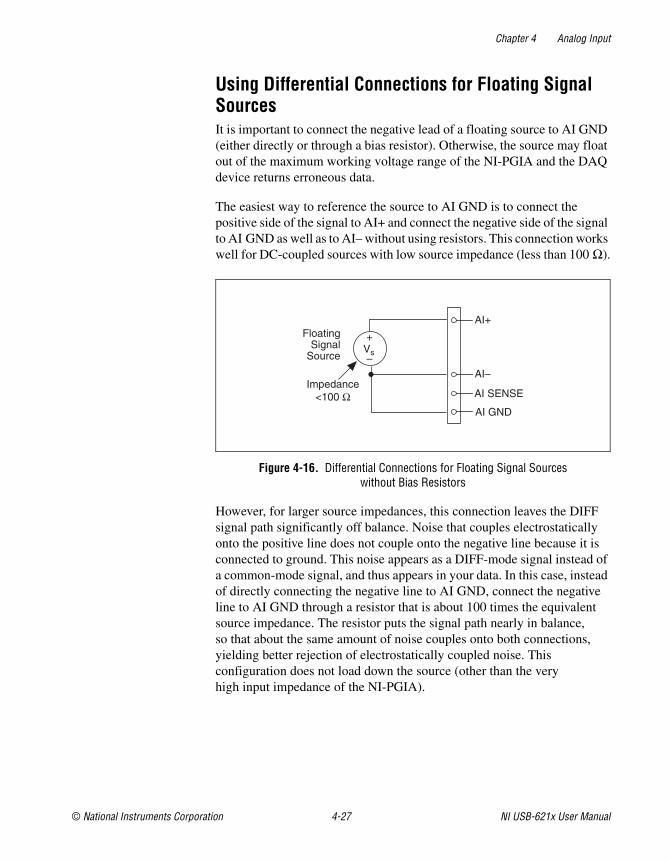
Chapter 4 Analog Input
© National Instruments Corporation 4-27 NI USB-621x User Manual
Using Differential Connections for Floating Signal SourcesIt is important to connect the negative lead of a floating source to AI GND (either directly or through a bias resistor). Otherwise, the source may float out of the maximum working voltage range of the NI-PGIA and the DAQ device returns erroneous data.
The easiest way to reference the source to AI GND is to connect the positive side of the signal to AI+ and connect the negative side of the signal to AI GND as well as to AI– without using resistors. This connection works well for DC-coupled sources with low source impedance (less than 100 Ω).
Figure 4-16. Differential Connections for Floating Signal Sources without Bias Resistors
However, for larger source impedances, this connection leaves the DIFF signal path significantly off balance. Noise that couples electrostatically onto the positive line does not couple onto the negative line because it is connected to ground. This noise appears as a DIFF-mode signal instead of a common-mode signal, and thus appears in your data. In this case, instead of directly connecting the negative line to AI GND, connect the negative line to AI GND through a resistor that is about 100 times the equivalent source impedance. The resistor puts the signal path nearly in balance, so that about the same amount of noise couples onto both connections, yielding better rejection of electrostatically coupled noise. This configuration does not load down the source (other than the very high input impedance of the NI-PGIA).
–
+
Impedance<100 Ω
AI GND
AI+
AI–
AI SENSE
Vs
FloatingSignal
Source
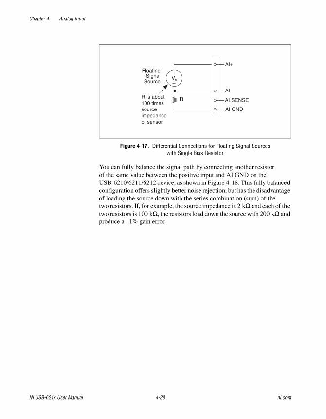
Chapter 4 Analog Input
NI USB-621x User Manual 4-28 ni.com
Figure 4-17. Differential Connections for Floating Signal Sources with Single Bias Resistor
You can fully balance the signal path by connecting another resistor of the same value between the positive input and AI GND on the USB-6210/6211/6212 device, as shown in Figure 4-18. This fully balanced configuration offers slightly better noise rejection, but has the disadvantage of loading the source down with the series combination (sum) of the two resistors. If, for example, the source impedance is 2 kΩ and each of the two resistors is 100 kΩ, the resistors load down the source with 200 kΩ and produce a –1% gain error.
–
+
R is about 100 times source impedanceof sensor
AI GND
R
Vs
FloatingSignal
Source
AI+
AI–
AI SENSE
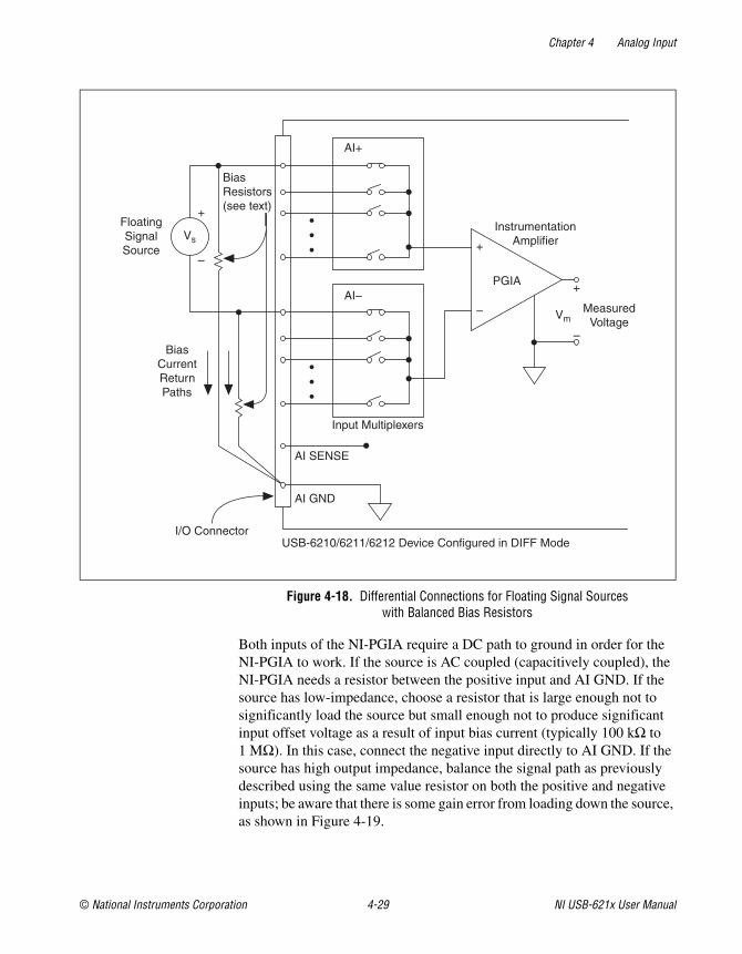
Chapter 4 Analog Input
© National Instruments Corporation 4-29 NI USB-621x User Manual
Figure 4-18. Differential Connections for Floating Signal Sources with Balanced Bias Resistors
Both inputs of the NI-PGIA require a DC path to ground in order for the NI-PGIA to work. If the source is AC coupled (capacitively coupled), the NI-PGIA needs a resistor between the positive input and AI GND. If the source has low-impedance, choose a resistor that is large enough not to significantly load the source but small enough not to produce significant input offset voltage as a result of input bias current (typically 100 kΩ to 1 MΩ). In this case, connect the negative input directly to AI GND. If the source has high output impedance, balance the signal path as previously described using the same value resistor on both the positive and negative inputs; be aware that there is some gain error from loading down the source, as shown in Figure 4-19.
USB-6210/6211/6212 Device Configured in DIFF Mode
PGIA
–
+
–
+
–
+
FloatingSignalSource
Bias Current Return Paths
AI GND
AI SENSE
Input Multiplexers
MeasuredVoltage
InstrumentationAmplifier
AI+
AI–
I/O Connector
BiasResistors(see text)
Vs
Vm
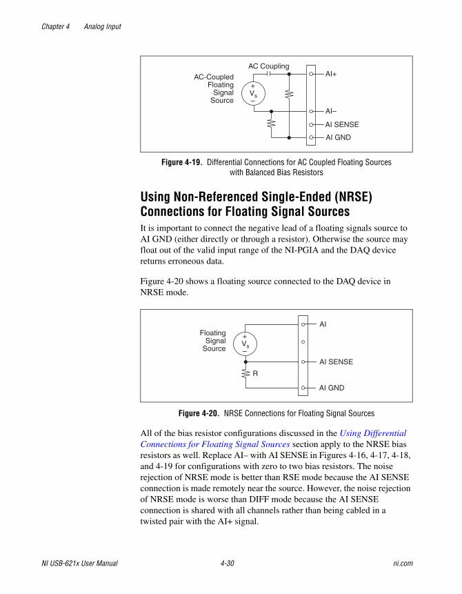
Chapter 4 Analog Input
NI USB-621x User Manual 4-30 ni.com
Figure 4-19. Differential Connections for AC Coupled Floating Sources with Balanced Bias Resistors
Using Non-Referenced Single-Ended (NRSE) Connections for Floating Signal SourcesIt is important to connect the negative lead of a floating signals source to AI GND (either directly or through a resistor). Otherwise the source may float out of the valid input range of the NI-PGIA and the DAQ device returns erroneous data.
Figure 4-20 shows a floating source connected to the DAQ device in NRSE mode.
Figure 4-20. NRSE Connections for Floating Signal Sources
All of the bias resistor configurations discussed in the Using Differential Connections for Floating Signal Sources section apply to the NRSE bias resistors as well. Replace AI– with AI SENSE in Figures 4-16, 4-17, 4-18, and 4-19 for configurations with zero to two bias resistors. The noise rejection of NRSE mode is better than RSE mode because the AI SENSE connection is made remotely near the source. However, the noise rejection of NRSE mode is worse than DIFF mode because the AI SENSE connection is shared with all channels rather than being cabled in a twisted pair with the AI+ signal.
–
+
AI GND
Vs
AC-CoupledFloating
SignalSource
AI+
AI–
AI SENSE
AC Coupling
–
+
AI GND
R
AI SENSE
AI
Vs
FloatingSignal
Source
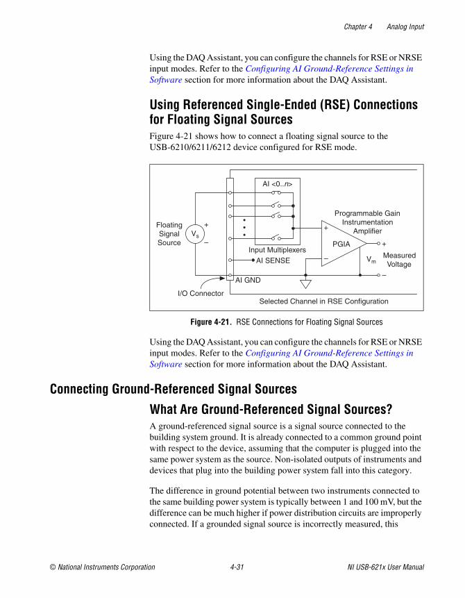
Chapter 4 Analog Input
© National Instruments Corporation 4-31 NI USB-621x User Manual
Using the DAQ Assistant, you can configure the channels for RSE or NRSE input modes. Refer to the Configuring AI Ground-Reference Settings in Software section for more information about the DAQ Assistant.
Using Referenced Single-Ended (RSE) Connections for Floating Signal SourcesFigure 4-21 shows how to connect a floating signal source to the USB-6210/6211/6212 device configured for RSE mode.
Figure 4-21. RSE Connections for Floating Signal Sources
Using the DAQ Assistant, you can configure the channels for RSE or NRSE input modes. Refer to the Configuring AI Ground-Reference Settings in Software section for more information about the DAQ Assistant.
Connecting Ground-Referenced Signal Sources
What Are Ground-Referenced Signal Sources?A ground-referenced signal source is a signal source connected to the building system ground. It is already connected to a common ground point with respect to the device, assuming that the computer is plugged into the same power system as the source. Non-isolated outputs of instruments and devices that plug into the building power system fall into this category.
The difference in ground potential between two instruments connected to the same building power system is typically between 1 and 100 mV, but the difference can be much higher if power distribution circuits are improperly connected. If a grounded signal source is incorrectly measured, this
Selected Channel in RSE Configuration
PGIA Input Multiplexers
–
+
–
Floating Signal Source
Vs
I/O Connector
AI GND
AI SENSE
AI <0..n>
+
Programmable Gain Instrumentation
Amplifier
Measured Voltage
Vm
–
+
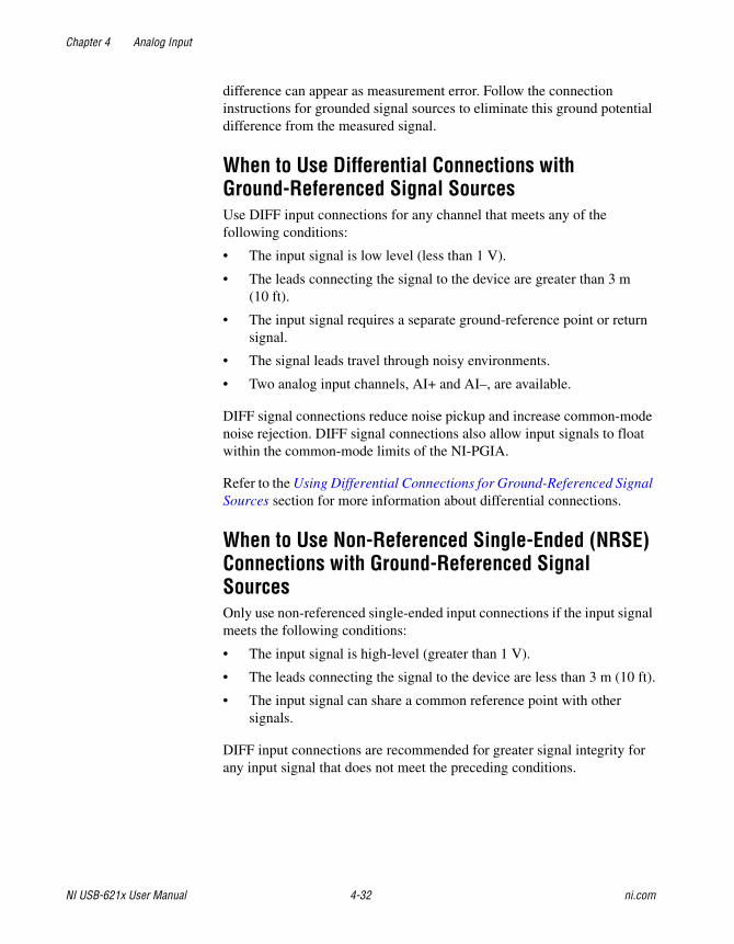
Chapter 4 Analog Input
NI USB-621x User Manual 4-32 ni.com
difference can appear as measurement error. Follow the connection instructions for grounded signal sources to eliminate this ground potential difference from the measured signal.
When to Use Differential Connections with Ground-Referenced Signal SourcesUse DIFF input connections for any channel that meets any of the following conditions:
• The input signal is low level (less than 1 V).
• The leads connecting the signal to the device are greater than 3 m (10 ft).
• The input signal requires a separate ground-reference point or return signal.
• The signal leads travel through noisy environments.
• Two analog input channels, AI+ and AI–, are available.
DIFF signal connections reduce noise pickup and increase common-mode noise rejection. DIFF signal connections also allow input signals to float within the common-mode limits of the NI-PGIA.
Refer to the Using Differential Connections for Ground-Referenced Signal Sources section for more information about differential connections.
When to Use Non-Referenced Single-Ended (NRSE) Connections with Ground-Referenced Signal SourcesOnly use non-referenced single-ended input connections if the input signal meets the following conditions:
• The input signal is high-level (greater than 1 V).
• The leads connecting the signal to the device are less than 3 m (10 ft).
• The input signal can share a common reference point with other signals.
DIFF input connections are recommended for greater signal integrity for any input signal that does not meet the preceding conditions.
Chapter 4 Analog Input
© National Instruments Corporation 4-33 NI USB-621x User Manual
In the single-ended modes, more electrostatic and magnetic noise couples into the signal connections than in DIFF configurations. The coupling is the result of differences in the signal path. Magnetic coupling is proportional to the area between the two signal conductors. Electrical coupling is a function of how much the electric field differs between the two conductors.
With this type of connection, the NI-PGIA rejects both the common-mode noise in the signal and the ground potential difference between the signal source and the device ground.
Refer to the Using Non-Referenced Single-Ended (NRSE) Connections for Ground-Referenced Signal Sources section for more information about NRSE connections.
When to Use Referenced Single-Ended (RSE) Connections with Ground-Referenced Signal SourcesDo not use RSE connections with ground-referenced signal sources. Use NRSE or DIFF connections instead.
As shown in the bottom-rightmost cell of Table 4-2, there can be a potential difference between AI GND and the ground of the sensor. In RSE mode, this ground loop causes measurement errors.
Using Differential Connections for Ground-Referenced Signal SourcesFigure 4-22 shows how to connect a ground-referenced signal source to the USB-6210/6211/6212 device configured in DIFF mode.
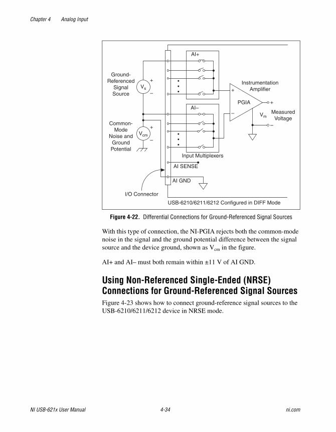
Chapter 4 Analog Input
NI USB-621x User Manual 4-34 ni.com
Figure 4-22. Differential Connections for Ground-Referenced Signal Sources
With this type of connection, the NI-PGIA rejects both the common-mode noise in the signal and the ground potential difference between the signal source and the device ground, shown as Vcm in the figure.
AI+ and AI– must both remain within ±11 V of AI GND.
Using Non-Referenced Single-Ended (NRSE) Connections for Ground-Referenced Signal SourcesFigure 4-23 shows how to connect ground-reference signal sources to the USB-6210/6211/6212 device in NRSE mode.
USB-6210/6211/6212 Configured in DIFF Mode
PGIA
–
+
–
+
–
+
–
+
Vcm
Vs
Ground-Referenced
SignalSource
Common-Mode
Noise andGroundPotential
AI GND
AI SENSE
Input Multiplexers
Vm Measured
Voltage
Instrumentation Amplifier
AI+
AI–
I/O Connector
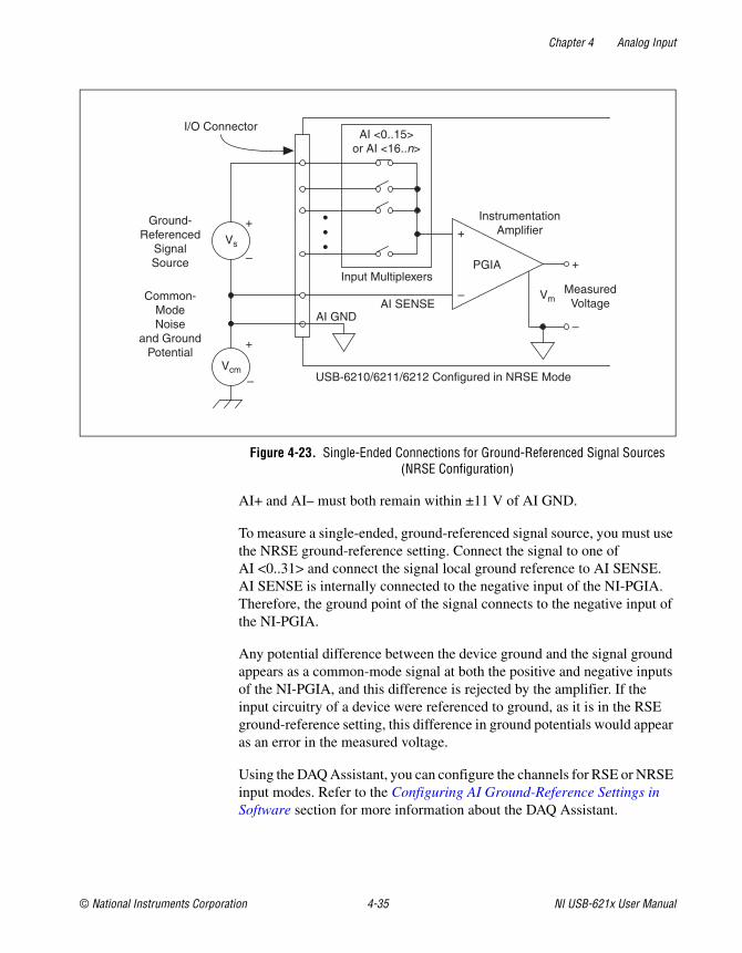
Chapter 4 Analog Input
© National Instruments Corporation 4-35 NI USB-621x User Manual
Figure 4-23. Single-Ended Connections for Ground-Referenced Signal Sources (NRSE Configuration)
AI+ and AI– must both remain within ±11 V of AI GND.
To measure a single-ended, ground-referenced signal source, you must use the NRSE ground-reference setting. Connect the signal to one of AI <0..31> and connect the signal local ground reference to AI SENSE. AI SENSE is internally connected to the negative input of the NI-PGIA. Therefore, the ground point of the signal connects to the negative input of the NI-PGIA.
Any potential difference between the device ground and the signal ground appears as a common-mode signal at both the positive and negative inputs of the NI-PGIA, and this difference is rejected by the amplifier. If the input circuitry of a device were referenced to ground, as it is in the RSE ground-reference setting, this difference in ground potentials would appear as an error in the measured voltage.
Using the DAQ Assistant, you can configure the channels for RSE or NRSE input modes. Refer to the Configuring AI Ground-Reference Settings in Software section for more information about the DAQ Assistant.
USB-6210/6211/6212 Configured in NRSE Mode
Common-ModeNoise
and GroundPotential
Ground-Referenced
SignalSource PGIA
Input Multiplexers
–
+
–
+
Vs
Vcm
I/O Connector
AI GNDAI SENSE
AI <0..15>or AI <16..n>
–
+
InstrumentationAmplifier
MeasuredVoltage
Vm
–
+
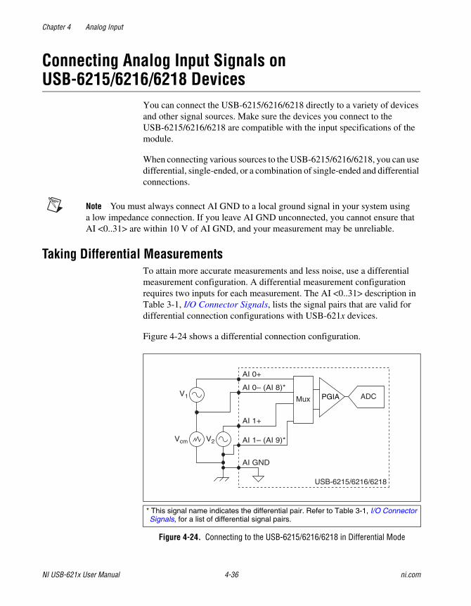
Chapter 4 Analog Input
NI USB-621x User Manual 4-36 ni.com
Connecting Analog Input Signals on USB-6215/6216/6218 Devices
You can connect the USB-6215/6216/6218 directly to a variety of devices and other signal sources. Make sure the devices you connect to the USB-6215/6216/6218 are compatible with the input specifications of the module.
When connecting various sources to the USB-6215/6216/6218, you can use differential, single-ended, or a combination of single-ended and differential connections.
Note You must always connect AI GND to a local ground signal in your system using a low impedance connection. If you leave AI GND unconnected, you cannot ensure that AI <0..31> are within 10 V of AI GND, and your measurement may be unreliable.
Taking Differential MeasurementsTo attain more accurate measurements and less noise, use a differential measurement configuration. A differential measurement configuration requires two inputs for each measurement. The AI <0..31> description in Table 3-1, I/O Connector Signals, lists the signal pairs that are valid for differential connection configurations with USB-621x devices.
Figure 4-24 shows a differential connection configuration.
Figure 4-24. Connecting to the USB-6215/6216/6218 in Differential Mode
* This signal name indicates the differential pair. Refer to Table 3-1, I/O Connector Signals, for a list of differential signal pairs.
AI 0+
AI 0– (AI 8)*
Mux
AI 1+
AI 1– (AI 9)*
AI GND
V1
V2Vcm
ADCPGIA
USB-6215/6216/6218
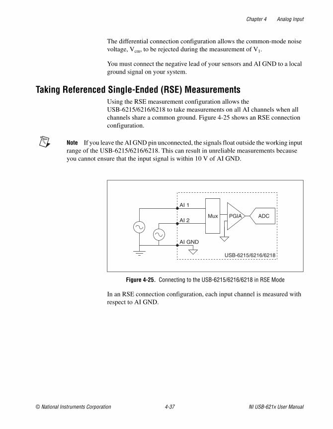
Chapter 4 Analog Input
© National Instruments Corporation 4-37 NI USB-621x User Manual
The differential connection configuration allows the common-mode noise voltage, Vcm, to be rejected during the measurement of V1.
You must connect the negative lead of your sensors and AI GND to a local ground signal on your system.
Taking Referenced Single-Ended (RSE) MeasurementsUsing the RSE measurement configuration allows the USB-6215/6216/6218 to take measurements on all AI channels when all channels share a common ground. Figure 4-25 shows an RSE connection configuration.
Note If you leave the AI GND pin unconnected, the signals float outside the working input range of the USB-6215/6216/6218. This can result in unreliable measurements because you cannot ensure that the input signal is within 10 V of AI GND.
Figure 4-25. Connecting to the USB-6215/6216/6218 in RSE Mode
In an RSE connection configuration, each input channel is measured with respect to AI GND.
AI 1
AI 2
AI GND
USB-6215/6216/6218
Mux ADCPGIA
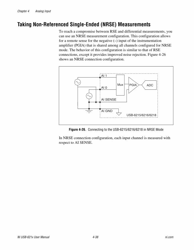
Chapter 4 Analog Input
NI USB-621x User Manual 4-38 ni.com
Taking Non-Referenced Single-Ended (NRSE) MeasurementsTo reach a compromise between RSE and differential measurements, you can use an NRSE measurement configuration. This configuration allows for a remote sense for the negative (–) input of the instrumentation amplifier (PGIA) that is shared among all channels configured for NRSE mode. The behavior of this configuration is similar to that of RSE connections, except it provides improved noise rejection. Figure 4-26 shows an NRSE connection configuration.
Figure 4-26. Connecting to the USB-6215/6216/6218 in NRSE Mode
In NRSE connection configuration, each input channel is measured with respect to AI SENSE.
AI 1
AI 0
AI GND
Mux ADCPGIA
AI SENSE
USB-6215/6216/6218
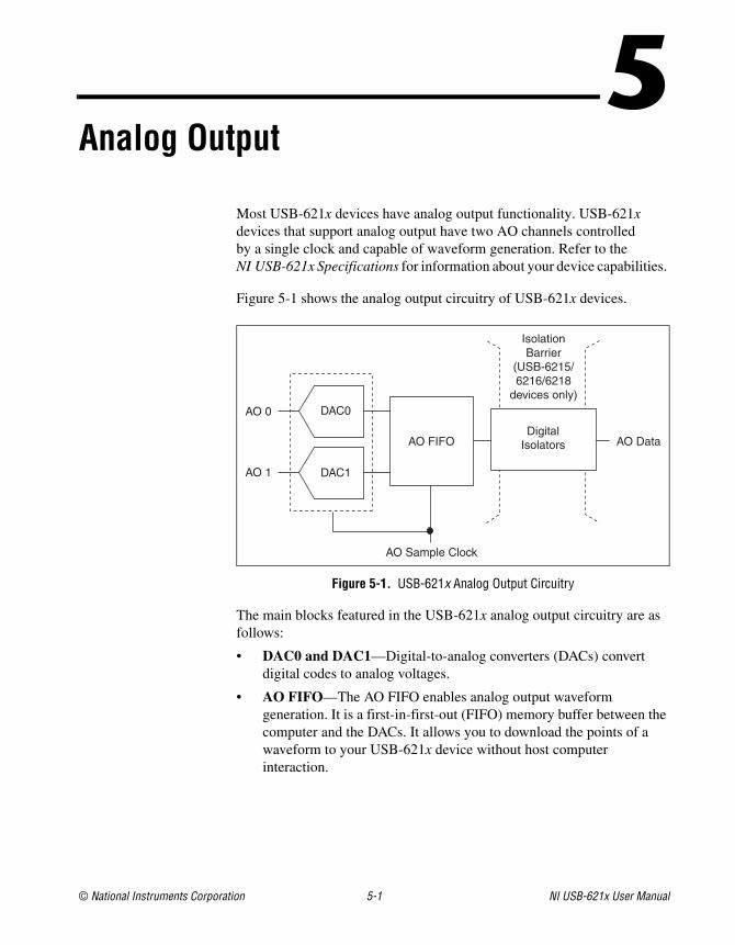
© National Instruments Corporation 5-1 NI USB-621x User Manual
5Analog Output
Most USB-621x devices have analog output functionality. USB-621x devices that support analog output have two AO channels controlled by a single clock and capable of waveform generation. Refer to the NI USB-621x Specifications for information about your device capabilities.
Figure 5-1 shows the analog output circuitry of USB-621x devices.
Figure 5-1. USB-621x Analog Output Circuitry
The main blocks featured in the USB-621x analog output circuitry are as follows:
• DAC0 and DAC1—Digital-to-analog converters (DACs) convert digital codes to analog voltages.
• AO FIFO—The AO FIFO enables analog output waveform generation. It is a first-in-first-out (FIFO) memory buffer between the computer and the DACs. It allows you to download the points of a waveform to your USB-621x device without host computer interaction.
AO Sample Clock
AO DataAO FIFO
AO 0
AO 1
DAC0
DAC1
IsolationBarrier
(USB-6215/6216/6218
devices only)
DigitalIsolators
Chapter 5 Analog Output
NI USB-621x User Manual 5-2 ni.com
• AO Sample Clock—The AO Sample Clock signal reads a sample from the DAC FIFO and generates the AO voltage. Refer to the AO Sample Clock Signal section for more information.
• Isolation Barrier and Digital Isolators—Refer to Chapter 9, Isolation and Digital Isolators on USB-6215/6216/6218 Devices, for more information.
AO RangeThe AO range is ±10 V for USB-621x devices.
Minimizing Glitches on the Output SignalWhen you use a DAC to generate a waveform, you may observe glitches on the output signal. These glitches are normal; when a DAC switches from one voltage to another, it produces glitches due to released charges. The largest glitches occur when the most significant bit of the DAC code changes. You can build a lowpass deglitching filter to remove some of these glitches, depending on the frequency and nature of the output signal. Visit ni.com/support for more information about minimizing glitches.
Analog Output Data Generation MethodsWhen performing an analog output operation, you can perform software-timed or hardware-timed generations:
• Software-timed generations—Software controls the rate at which data is generated. Software sends a separate command to the hardware to initiate each DAC conversion. In NI-DAQmx, software-timed generations are referred to as on-demand timing. Software-timed generations are also referred to as immediate or static operations. They are typically used for writing a single value out, such as a constant DC voltage.
• Hardware-timed generations—A digital hardware signal controls the rate of the generation. This signal can be generated internally on your device or provided externally.
Hardware-timed generations have several advantages over software-timed acquisitions:
– The time between samples can be much shorter.
– The timing between samples can be deterministic.
Chapter 5 Analog Output
© National Instruments Corporation 5-3 NI USB-621x User Manual
– Hardware-timed acquisitions can use hardware triggering.
Hardware-timed operations are buffered. During hardware-timed AO generation, data is moved from a PC buffer to the onboard FIFO on the USB-621x device using USB Signal Streams before it is written to the DACs one sample at a time. Buffered acquisitions allow for fast transfer rates because data is moved in large blocks rather than one point at a time.
One property of buffered I/O operations is the sample mode. The sample mode can be either finite or continuous.
Finite sample mode generation refers to the generation of a specific, predetermined number of data samples. Once the specified number of samples has been written out, the generation stops.
Continuous generation refers to the generation of an unspecified number of samples. Instead of generating a set number of data samples and stopping, a continuous generation continues until you stop the operation. There are several different methods of continuous generation that control what data is written. These methods are regeneration, FIFO regeneration, and non-regeneration modes.
Regeneration is the repetition of the data that is already in the buffer. Standard regeneration is when data from the PC buffer is continually downloaded to the FIFO to be written out. New data can be written to the PC buffer at any time without disrupting the output.
With FIFO regeneration, the entire buffer is downloaded to the FIFO and regenerated from there. Once the data is downloaded, new data cannot be written to the FIFO. To use FIFO regeneration, the entire buffer must fit within the FIFO size. The advantage of using FIFO regeneration is that it does not require communication with the main host memory once the operation is started, thereby preventing any problems that may occur due to excessive bus traffic.
With non-regeneration, old data is not repeated. New data must be continually written to the buffer. If the program does not write new data to the buffer at a fast enough rate to keep up with the generation, the buffer underflows and causes an error.
Analog Output Digital TriggeringAnalog output supports two different triggering actions:
• Start trigger
• Pause trigger
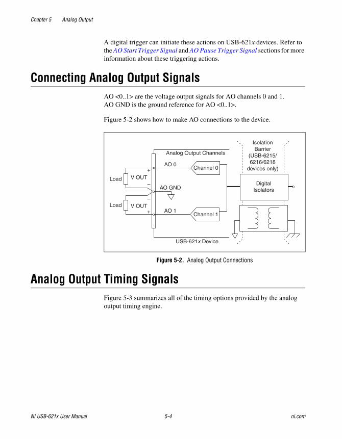
Chapter 5 Analog Output
NI USB-621x User Manual 5-4 ni.com
A digital trigger can initiate these actions on USB-621x devices. Refer to the AO Start Trigger Signal and AO Pause Trigger Signal sections for more information about these triggering actions.
Connecting Analog Output SignalsAO <0..1> are the voltage output signals for AO channels 0 and 1. AO GND is the ground reference for AO <0..1>.
Figure 5-2 shows how to make AO connections to the device.
Figure 5-2. Analog Output Connections
Analog Output Timing SignalsFigure 5-3 summarizes all of the timing options provided by the analog output timing engine.
Load
Load
V OUT
V OUT
+
–
+
–
AO GND
AO 1
Analog Output Channels
USB-621x Device
AO 0
Channel 1
Channel 0
DigitalIsolators
IsolationBarrier
(USB-6215/6216/6218
devices only)
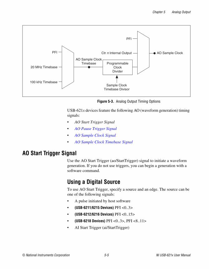
Chapter 5 Analog Output
© National Instruments Corporation 5-5 NI USB-621x User Manual
Figure 5-3. Analog Output Timing Options
USB-621x devices feature the following AO (waveform generation) timing signals:
• AO Start Trigger Signal
• AO Pause Trigger Signal
• AO Sample Clock Signal
• AO Sample Clock Timebase Signal
AO Start Trigger SignalUse the AO Start Trigger (ao/StartTrigger) signal to initiate a waveform generation. If you do not use triggers, you can begin a generation with a software command.
Using a Digital SourceTo use AO Start Trigger, specify a source and an edge. The source can be one of the following signals:
• A pulse initiated by host software
• (USB-6211/6215 Devices) PFI <0..3>
• (USB-6212/6216 Devices) PFI <0..15>
• (USB-6218 Devices) PFI <0..3>, PFI <8..11>
• AI Start Trigger (ai/StartTrigger)
20 MHz Timebase
100 kHz Timebase
Programmable Clock
Divider
AO Sample ClockTimebase
Ctr n Internal Output AO Sample ClockPFI
PFI
Sample ClockTimebase Divisor
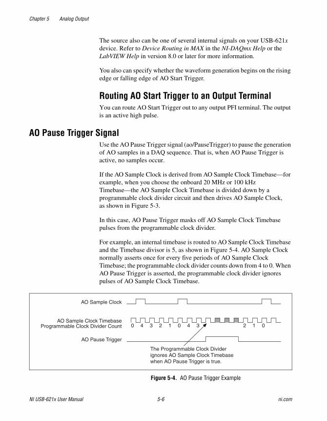
Chapter 5 Analog Output
NI USB-621x User Manual 5-6 ni.com
The source also can be one of several internal signals on your USB-621x device. Refer to Device Routing in MAX in the NI-DAQmx Help or the LabVIEW Help in version 8.0 or later for more information.
You also can specify whether the waveform generation begins on the rising edge or falling edge of AO Start Trigger.
Routing AO Start Trigger to an Output TerminalYou can route AO Start Trigger out to any output PFI terminal. The output is an active high pulse.
AO Pause Trigger SignalUse the AO Pause Trigger signal (ao/PauseTrigger) to pause the generation of AO samples in a DAQ sequence. That is, when AO Pause Trigger is active, no samples occur.
If the AO Sample Clock is derived from AO Sample Clock Timebase—for example, when you choose the onboard 20 MHz or 100 kHz Timebase—the AO Sample Clock Timebase is divided down by a programmable clock divider circuit and then drives AO Sample Clock, as shown in Figure 5-3.
In this case, AO Pause Trigger masks off AO Sample Clock Timebase pulses from the programmable clock divider.
For example, an internal timebase is routed to AO Sample Clock Timebase and the Timebase divisor is 5, as shown in Figure 5-4. AO Sample Clock normally asserts once for every five periods of AO Sample Clock Timebase; the programmable clock divider counts down from 4 to 0. When AO Pause Trigger is asserted, the programmable clock divider ignores pulses of AO Sample Clock Timebase.
Figure 5-4. AO Pause Trigger Example
AO Pause Trigger
AO Sample Clock Timebase
AO Sample Clock
0 4 3 2 1 0 4 3Programmable Clock Divider Count 2 1 0
The Programmable Clock Dividerignores AO Sample Clock Timebasewhen AO Pause Trigger is true.
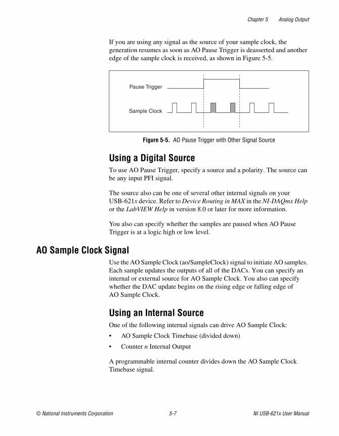
Chapter 5 Analog Output
© National Instruments Corporation 5-7 NI USB-621x User Manual
If you are using any signal as the source of your sample clock, the generation resumes as soon as AO Pause Trigger is deasserted and another edge of the sample clock is received, as shown in Figure 5-5.
Figure 5-5. AO Pause Trigger with Other Signal Source
Using a Digital SourceTo use AO Pause Trigger, specify a source and a polarity. The source can be any input PFI signal.
The source also can be one of several other internal signals on your USB-621x device. Refer to Device Routing in MAX in the NI-DAQmx Help or the LabVIEW Help in version 8.0 or later for more information.
You also can specify whether the samples are paused when AO Pause Trigger is at a logic high or low level.
AO Sample Clock SignalUse the AO Sample Clock (ao/SampleClock) signal to initiate AO samples. Each sample updates the outputs of all of the DACs. You can specify an internal or external source for AO Sample Clock. You also can specify whether the DAC update begins on the rising edge or falling edge of AO Sample Clock.
Using an Internal SourceOne of the following internal signals can drive AO Sample Clock:
• AO Sample Clock Timebase (divided down)
• Counter n Internal Output
A programmable internal counter divides down the AO Sample Clock Timebase signal.
Pause Trigger
Sample Clock
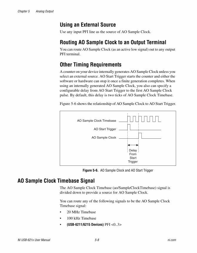
Chapter 5 Analog Output
NI USB-621x User Manual 5-8 ni.com
Using an External SourceUse any input PFI line as the source of AO Sample Clock.
Routing AO Sample Clock to an Output TerminalYou can route AO Sample Clock (as an active low signal) out to any output PFI terminal.
Other Timing RequirementsA counter on your device internally generates AO Sample Clock unless you select an external source. AO Start Trigger starts the counter and either the software or hardware can stop it once a finite generation completes. When using an internally generated AO Sample Clock, you also can specify a configurable delay from AO Start Trigger to the first AO Sample Clock pulse. By default, this delay is two ticks of AO Sample Clock Timebase.
Figure 5-6 shows the relationship of AO Sample Clock to AO Start Trigger.
Figure 5-6. AO Sample Clock and AO Start Trigger
AO Sample Clock Timebase SignalThe AO Sample Clock Timebase (ao/SampleClockTimebase) signal is divided down to provide a source for AO Sample Clock.
You can route any of the following signals to be the AO Sample Clock Timebase signal:
• 20 MHz Timebase
• 100 kHz Timebase
• (USB-6211/6215 Devices) PFI <0..3>
AO Sample Clock Timebase
AO Start Trigger
AO Sample Clock
Delay From Start
Trigger
Chapter 5 Analog Output
© National Instruments Corporation 5-9 NI USB-621x User Manual
• (USB-6212/6216 Devices) PFI <0..15>
• (USB-6218 Devices) PFI <0..3>, PFI <8..11>
AO Sample Clock Timebase is not available as an output on the I/O connector.
You might use AO Sample Clock Timebase if you want to use an external sample clock signal, but need to divide the signal down. If you want to use an external sample clock signal, but do not need to divide the signal, then you should use AO Sample Clock rather than AO Sample Clock Timebase.
Getting Started with AO Applications in SoftwareYou can use a USB-621x device in the following analog output applications:
• Single-point (on-demand) generation
• Finite generation
• Continuous generation
• Waveform generation
You can perform these generations through programmed I/O or USB Signal Stream data transfer mechanisms. Some of the applications also use start triggers and pause triggers.
Note For more information about programming analog output applications and triggers in software, refer to the NI-DAQmx Help or the LabVIEW Help in version 8.0 or later.
© National Instruments Corporation 6-1 NI USB-621x User Manual
6Digital I/O
Refer to one of the following sections, depending on your device:
• Digital I/O on USB-6210/6211/6215/6218 Devices— USB-6210/6211/6215/6218 devices have up to eight lines of digital inputs (DI) and up to eight lines of digital output (DO).
• Digital I/O on USB-6212/6216 Devices—USB-6212/6216 devices have up to 32 bidirectional static digital I/O (DIO) lines.
Digital I/O on USB-6210/6211/6215/6218 DevicesUSB-6210/6211/6215/6218 devices have up to eight static digital input lines, P0.<0..7>. These lines also can be used as PFI inputs.
USB-6210/6211/6215/6218 devices have up to eight static digital output lines, P1.<0..7>. These lines also can be used as PFI output. By default the digital output lines are disabled (high impedance with a 47 kΩ pull-down resistor) on power up. Software can enable or disable the entire port (software cannot enable individual lines). Once the port is enabled, you can individually configure each line to the following:
• Set a line to a static 0
• Set a line to a static 1
• Export a timing output signal to a line as a PFI pin
The voltage input and output levels and the current drive level of the DI and DO lines are listed in the NI USB-621x Specifications. Refer to Chapter 7, PFI, for more information on PFI inputs and outputs.
Figure 6-1 shows the circuitry of one DI line and one DO line. The following sections provide information about the various parts of the DIO circuit.
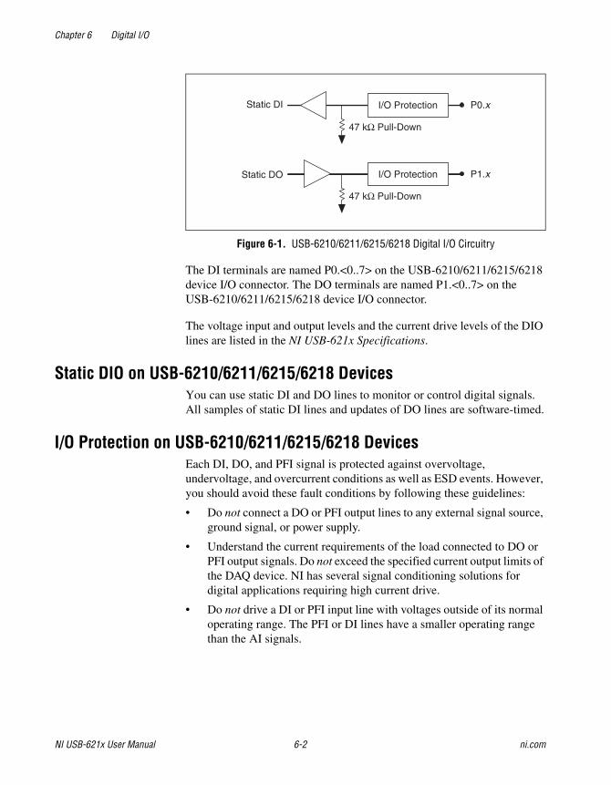
Chapter 6 Digital I/O
NI USB-621x User Manual 6-2 ni.com
Figure 6-1. USB-6210/6211/6215/6218 Digital I/O Circuitry
The DI terminals are named P0.<0..7> on the USB-6210/6211/6215/6218 device I/O connector. The DO terminals are named P1.<0..7> on the USB-6210/6211/6215/6218 device I/O connector.
The voltage input and output levels and the current drive levels of the DIO lines are listed in the NI USB-621x Specifications.
Static DIO on USB-6210/6211/6215/6218 DevicesYou can use static DI and DO lines to monitor or control digital signals. All samples of static DI lines and updates of DO lines are software-timed.
I/O Protection on USB-6210/6211/6215/6218 DevicesEach DI, DO, and PFI signal is protected against overvoltage, undervoltage, and overcurrent conditions as well as ESD events. However, you should avoid these fault conditions by following these guidelines:
• Do not connect a DO or PFI output lines to any external signal source, ground signal, or power supply.
• Understand the current requirements of the load connected to DO or PFI output signals. Do not exceed the specified current output limits of the DAQ device. NI has several signal conditioning solutions for digital applications requiring high current drive.
• Do not drive a DI or PFI input line with voltages outside of its normal operating range. The PFI or DI lines have a smaller operating range than the AI signals.
Static DI I/O Protection
47 kΩ Pull-Down
P0.x
I/O Protection
47 kΩ Pull-Down
P1.xStatic DO
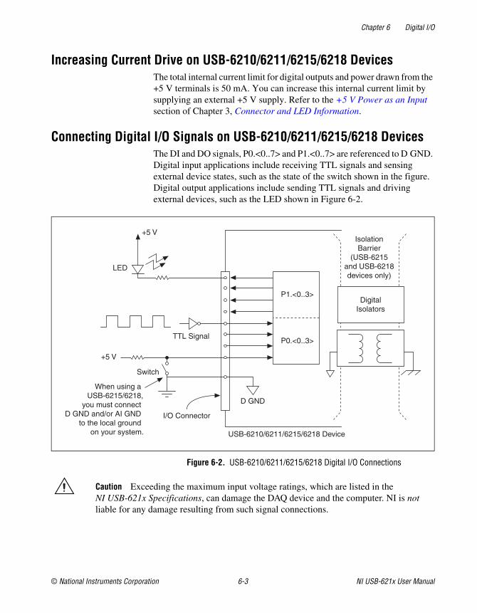
Chapter 6 Digital I/O
© National Instruments Corporation 6-3 NI USB-621x User Manual
Increasing Current Drive on USB-6210/6211/6215/6218 DevicesThe total internal current limit for digital outputs and power drawn from the +5 V terminals is 50 mA. You can increase this internal current limit by supplying an external +5 V supply. Refer to the +5 V Power as an Input section of Chapter 3, Connector and LED Information.
Connecting Digital I/O Signals on USB-6210/6211/6215/6218 DevicesThe DI and DO signals, P0.<0..7> and P1.<0..7> are referenced to D GND. Digital input applications include receiving TTL signals and sensing external device states, such as the state of the switch shown in the figure. Digital output applications include sending TTL signals and driving external devices, such as the LED shown in Figure 6-2.
Figure 6-2. USB-6210/6211/6215/6218 Digital I/O Connections
Caution Exceeding the maximum input voltage ratings, which are listed in the NI USB-621x Specifications, can damage the DAQ device and the computer. NI is not liable for any damage resulting from such signal connections.
+5 V
LED
TTL Signal
+5 V
Switch
I/O Connector
D GND
USB-6210/6211/6215/6218 Device
P0.<0..3>
P1.<0..3>Digital
Isolators
IsolationBarrier
(USB-6215and USB-6218devices only)
When using a USB-6215/6218,
you must connect D GND and/or AI GND
to the local ground on your system.
Chapter 6 Digital I/O
NI USB-621x User Manual 6-4 ni.com
Getting Started with DIO Applications in Software on USB-6210/6211/6215/6218 Devices
You can use the USB-6210/6211/6215/6218 device in the following digital I/O applications:
• Static digital input
• Static digital output
Note For more information about programming digital I/O applications and triggers in software, refer to the NI-DAQmx Help or the LabVIEW Help in version 8.0 or later.
Digital I/O on USB-6212/6216 DevicesUSB-6212/6216 devices contain:
• Up to 16 DIO signals (P0.<0..15>). Each signal can be individually configured as either:
– Static digital input
– Static digital output
• 16 PFI/DIO signals (PFI <0..7>/P1.<0..7> and PFI <8..15>/P2.<0..7>). Each signal can be individually configured as either:
– Static digital input
– Static digital output
– PFI input
– PFI output
Each pin is called PFI x when used as a PFI; each pin is named P1.x or P2.x when used as a digital input or output.
Figure 6-3 shows the circuitry of one DIO line. Each DIO line is similar. The voltage input and output levels and the current drive levels of the DIO lines are listed in the NI USB-621x Specifications.
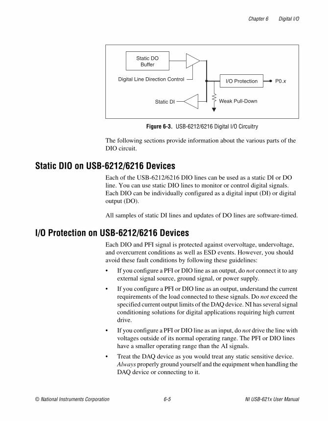
Chapter 6 Digital I/O
© National Instruments Corporation 6-5 NI USB-621x User Manual
Figure 6-3. USB-6212/6216 Digital I/O Circuitry
The following sections provide information about the various parts of the DIO circuit.
Static DIO on USB-6212/6216 DevicesEach of the USB-6212/6216 DIO lines can be used as a static DI or DO line. You can use static DIO lines to monitor or control digital signals. Each DIO can be individually configured as a digital input (DI) or digital output (DO).
All samples of static DI lines and updates of DO lines are software-timed.
I/O Protection on USB-6212/6216 DevicesEach DIO and PFI signal is protected against overvoltage, undervoltage, and overcurrent conditions as well as ESD events. However, you should avoid these fault conditions by following these guidelines:
• If you configure a PFI or DIO line as an output, do not connect it to any external signal source, ground signal, or power supply.
• If you configure a PFI or DIO line as an output, understand the current requirements of the load connected to these signals. Do not exceed the specified current output limits of the DAQ device. NI has several signal conditioning solutions for digital applications requiring high current drive.
• If you configure a PFI or DIO line as an input, do not drive the line with voltages outside of its normal operating range. The PFI or DIO lines have a smaller operating range than the AI signals.
• Treat the DAQ device as you would treat any static sensitive device. Always properly ground yourself and the equipment when handling the DAQ device or connecting to it.
Digital Line Direction Control
Static DI
I/O Protection
Weak Pull-Down
P0.x
Static DOBuffer
Chapter 6 Digital I/O
NI USB-621x User Manual 6-6 ni.com
Programmable Power-Up States on USB-6212/6216 DevicesAt system startup and reset, the hardware sets all PFI and DIO lines to high-impedance inputs by default. The DAQ device does not drive the signal high or low. Each line has a weak pull-down resistor connected to it, as described in the NI USB-621x Specifications.
NI-DAQmx supports programmable power-up states for PFI and DIO lines. Software can program any value at power up to the P0, P1, or P2 lines. The PFI and DIO lines can be set as:
• A high-impedance input with a weak pull-down resistor (default)
• An output driving a 0
• An output driving a 1
Refer to the NI-DAQmx Help or the LabVIEW Help in version 8.0 or later for more information about setting power-up states in NI-DAQmx or MAX.
Increasing Current Drive on USB-6212/6216 DevicesThe total internal current limit for digital outputs and power drawn from the +5 V terminals is 50 mA. You can increase this internal current limit by supplying an external +5 V supply. Refer to the +5 V Power as an Input section of Chapter 3, Connector and LED Information.
Connecting Digital I/O Signals on USB-6212/6216 DevicesThe DIO signals, P0.<0..15>, P1.<0..7>, and P2.<0..7> are referenced to D GND. You can individually program each line as an input or output. Figure 6-4 shows P0.<0..3> configured for digital input and P1.<0..3> configured for digital output. Digital input applications include receiving TTL signals and sensing external device states, such as the state of the switch shown in the figure. Digital output applications include sending TTL signals and driving external devices, such as the LED shown in the figure.
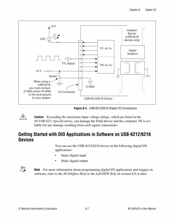
Chapter 6 Digital I/O
© National Instruments Corporation 6-7 NI USB-621x User Manual
Figure 6-4. USB-6212/6216 Digital I/O Connections
Caution Exceeding the maximum input voltage ratings, which are listed in the NI USB-621x Specifications, can damage the DAQ device and the computer. NI is not liable for any damage resulting from such signal connections.
Getting Started with DIO Applications in Software on USB-6212/6216 Devices
You can use the USB-6212/6216 device in the following digital I/O applications:
• Static digital input
• Static digital output
Note For more information about programming digital I/O applications and triggers in software, refer to the NI-DAQmx Help or the LabVIEW Help in version 8.0 or later.
+5 V
LED
TTL Signal
+5 V
Switch
I/O Connector
D GND
USB-6212/6216 Device
P0.<0..3>
P1.<0..3>Digital
Isolators
IsolationBarrier
(USB-6216devices only)
When using a USB-6216,
you must connect D GND and/or AI GND
to the local groundon your system.
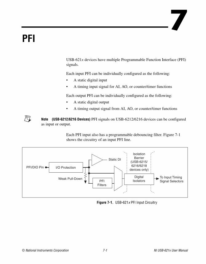
© National Instruments Corporation 7-1 NI USB-621x User Manual
7PFI
USB-621x devices have multiple Programmable Function Interface (PFI) signals.
Each input PFI can be individually configured as the following:
• A static digital input
• A timing input signal for AI, AO, or counter/timer functions
Each output PFI can be individually configured as the following:
• A static digital output
• A timing output signal from AI, AO, or counter/timer functions
Note (USB-6212/6216 Devices) PFI signals on USB-6212/6216 devices can be configured as input or output.
Each PFI input also has a programmable debouncing filter. Figure 7-1 shows the circuitry of an input PFI line.
Figure 7-1. USB-621x PFI Input Circuitry
Static DI
I/O Protection
To Input TimingSignal SelectorsPFI
Filters
Weak Pull-Down
PFI/DIO Pin
IsolationBarrier
(USB-6215/6216/6218
devices only)
DigitalIsolators
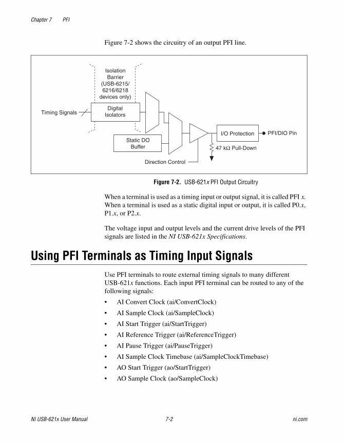
Chapter 7 PFI
NI USB-621x User Manual 7-2 ni.com
Figure 7-2 shows the circuitry of an output PFI line.
Figure 7-2. USB-621x PFI Output Circuitry
When a terminal is used as a timing input or output signal, it is called PFI x. When a terminal is used as a static digital input or output, it is called P0.x, P1.x, or P2.x.
The voltage input and output levels and the current drive levels of the PFI signals are listed in the NI USB-621x Specifications.
Using PFI Terminals as Timing Input SignalsUse PFI terminals to route external timing signals to many different USB-621x functions. Each input PFI terminal can be routed to any of the following signals:
• AI Convert Clock (ai/ConvertClock)
• AI Sample Clock (ai/SampleClock)
• AI Start Trigger (ai/StartTrigger)
• AI Reference Trigger (ai/ReferenceTrigger)
• AI Pause Trigger (ai/PauseTrigger)
• AI Sample Clock Timebase (ai/SampleClockTimebase)
• AO Start Trigger (ao/StartTrigger)
• AO Sample Clock (ao/SampleClock)
Timing Signals
Direction Control
I/O Protection
47 kΩ Pull-Down
PFI/DIO PinStatic DO
Buffer
IsolationBarrier
(USB-6215/6216/6218
devices only)
DigitalIsolators
Chapter 7 PFI
© National Instruments Corporation 7-3 NI USB-621x User Manual
• AO Sample Clock Timebase (ao/SampleClockTimebase)
• AO Pause Trigger (ao/PauseTrigger)
• Counter input signals for either counter—Source, Gate, Aux, HW_Arm, A, B, Z
Most functions allow you to configure the polarity of PFI inputs and whether the input is edge or level sensitive.
Exporting Timing Output Signals Using PFI TerminalsYou can route any of the following timing signals to any PFI output terminal:
• AI Convert Clock* (ai/ConvertClock)
• AI Hold Complete Event (ai/HoldCompleteEvent)
• AI Reference Trigger (ai/ReferenceTrigger)
• AI Sample Clock (ai/SampleClock)
• AI Start Trigger (ai/StartTrigger)
• AO Sample Clock* (ao/SampleClock)
• AO Start Trigger (ao/StartTrigger)
• Counter n Source
• Counter n Gate
• Counter n Internal Output
• Frequency Output
Note Signals with a * are inverted before being driven to a terminal; that is, these signals are active low.
Using PFI Terminals as Static Digital I/OsEach input PFI line can be individually configured as a static digital input, called P0.x. Each output PFI line can be individually configured as a static digital output, called P1.x.1
1 On USB-6212/6216 devices, all PFI lines can be individually configured as static digital inputs or static digital outputs, called P0.x.
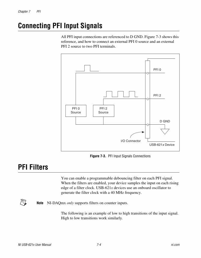
Chapter 7 PFI
NI USB-621x User Manual 7-4 ni.com
Connecting PFI Input SignalsAll PFI input connections are referenced to D GND. Figure 7-3 shows this reference, and how to connect an external PFI 0 source and an external PFI 2 source to two PFI terminals.
Figure 7-3. PFI Input Signals Connections
PFI FiltersYou can enable a programmable debouncing filter on each PFI signal. When the filters are enabled, your device samples the input on each rising edge of a filter clock. USB-621x devices use an onboard oscillator to generate the filter clock with a 40 MHz frequency.
Note NI-DAQmx only supports filters on counter inputs.
The following is an example of low to high transitions of the input signal. High to low transitions work similarly.
PFI 0 Source
PFI 2 Source
USB-621x Device
D GND
PFI 2
PFI 0
I/O Connector
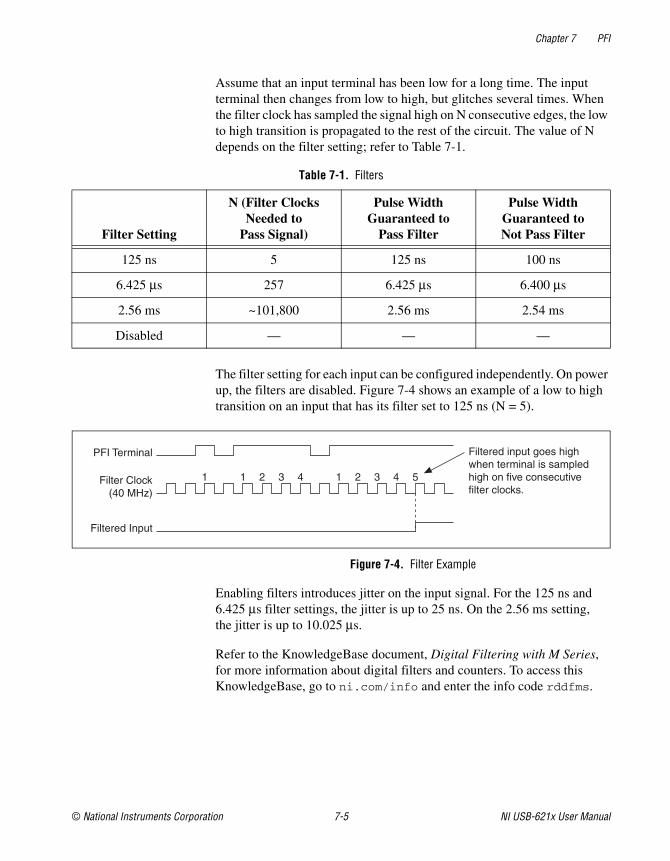
Chapter 7 PFI
© National Instruments Corporation 7-5 NI USB-621x User Manual
Assume that an input terminal has been low for a long time. The input terminal then changes from low to high, but glitches several times. When the filter clock has sampled the signal high on N consecutive edges, the low to high transition is propagated to the rest of the circuit. The value of N depends on the filter setting; refer to Table 7-1.
The filter setting for each input can be configured independently. On power up, the filters are disabled. Figure 7-4 shows an example of a low to high transition on an input that has its filter set to 125 ns (N = 5).
Figure 7-4. Filter Example
Enabling filters introduces jitter on the input signal. For the 125 ns and 6.425 μs filter settings, the jitter is up to 25 ns. On the 2.56 ms setting, the jitter is up to 10.025 μs.
Refer to the KnowledgeBase document, Digital Filtering with M Series, for more information about digital filters and counters. To access this KnowledgeBase, go to ni.com/info and enter the info code rddfms.
Table 7-1. Filters
Filter Setting
N (Filter Clocks Needed to
Pass Signal)
Pulse Width Guaranteed to
Pass Filter
Pulse Width Guaranteed to Not Pass Filter
125 ns 5 125 ns 100 ns
6.425 μs 257 6.425 μs 6.400 μs
2.56 ms ~101,800 2.56 ms 2.54 ms
Disabled — — —
1 2 3 1 4 1 2 3 4 5
PFI Terminal
Filter Clock (40 MHz)
Filtered Input
Filtered input goes high when terminal is sampled high on five consecutive filter clocks.
Chapter 7 PFI
NI USB-621x User Manual 7-6 ni.com
I/O ProtectionEach DI, DO, and PFI signal is protected against overvoltage, undervoltage, and overcurrent conditions as well as ESD events. However, you should avoid these fault conditions by following these guidelines:
• Do not connect a DO or PFI output lines to any external signal source, ground signal, or power supply.
• Understand the current requirements of the load connected to DO or PFI output signals. Do not exceed the specified current output limits of the DAQ device. NI has several signal conditioning solutions for digital applications requiring high current drive.
• Do not drive a DI or PFI input line with voltages outside of its normal operating range. The PFI or DI lines have a smaller operating range than the AI signals.
• Treat the DAQ device as you would treat any static sensitive device. Always properly ground yourself and the equipment when handling the DAQ device or connecting to it.
Programmable Power-Up StatesAt system startup and reset, the hardware sets all output PFI and DO lines to high-impedance by default. The DAQ device does not drive the signal high or low. Each line has a weak pull-down resistor connected to it, as described in the NI USB-621x Specifications.
NI-DAQmx supports programmable power-up states for PFI and DIO lines. Software can program any value at power up to the P1 lines. The output PFI and DO lines can be set as:
• A high-impedance input with a weak pull-down resistor (default)
• An output driving a 0
• An output driving a 1
Refer to the NI-DAQmx Help or the LabVIEW Help in version 8.0 or later for more information about setting power-up states in NI-DAQmx or MAX.
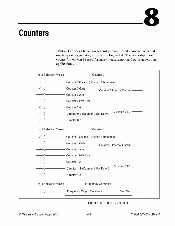
© National Instruments Corporation 8-1 NI USB-621x User Manual
8Counters
USB-621x devices have two general-purpose 32-bit counter/timers and one frequency generator, as shown in Figure 8-1. The general-purpose counter/timers can be used for many measurement and pulse generation applications.
Figure 8-1. USB-621x Counters
Counter 0
Counter 0 Source (Counter 0 Timebase)
Counter 0 Aux
Counter 0 HW Arm
Counter 0 A
Counter 0 B (Counter 0 Up_Down)
Counter 0 Z
Counter 0 Gate Counter 0 Internal Output
Counter 0 TC
Input Selection Muxes
Frequency Generator
Frequency Output Timebase Freq Out
Input Selection Muxes
Counter 1
Counter 1 Source (Counter 1 Timebase)
Counter 1 Aux
Counter 1 HW Arm
Counter 1 A
Counter 1 B (Counter 1 Up_Down)
Counter 1 Z
Counter 1 Gate Counter 0 Internal Output
Counter 0 TC
Input Selection Muxes
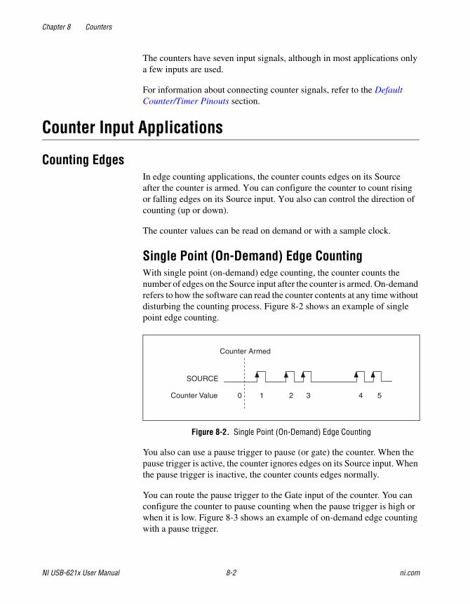
Chapter 8 Counters
NI USB-621x User Manual 8-2 ni.com
The counters have seven input signals, although in most applications only a few inputs are used.
For information about connecting counter signals, refer to the Default Counter/Timer Pinouts section.
Counter Input Applications
Counting EdgesIn edge counting applications, the counter counts edges on its Source after the counter is armed. You can configure the counter to count rising or falling edges on its Source input. You also can control the direction of counting (up or down).
The counter values can be read on demand or with a sample clock.
Single Point (On-Demand) Edge CountingWith single point (on-demand) edge counting, the counter counts the number of edges on the Source input after the counter is armed. On-demand refers to how the software can read the counter contents at any time without disturbing the counting process. Figure 8-2 shows an example of single point edge counting.
Figure 8-2. Single Point (On-Demand) Edge Counting
You also can use a pause trigger to pause (or gate) the counter. When the pause trigger is active, the counter ignores edges on its Source input. When the pause trigger is inactive, the counter counts edges normally.
You can route the pause trigger to the Gate input of the counter. You can configure the counter to pause counting when the pause trigger is high or when it is low. Figure 8-3 shows an example of on-demand edge counting with a pause trigger.
Counter Armed
SOURCE
Counter Value 1 0 5 4 3 2
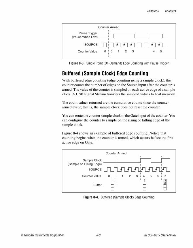
Chapter 8 Counters
© National Instruments Corporation 8-3 NI USB-621x User Manual
Figure 8-3. Single Point (On-Demand) Edge Counting with Pause Trigger
Buffered (Sample Clock) Edge CountingWith buffered edge counting (edge counting using a sample clock), the counter counts the number of edges on the Source input after the counter is armed. The value of the counter is sampled on each active edge of a sample clock. A USB Signal Stream transfers the sampled values to host memory.
The count values returned are the cumulative counts since the counter armed event; that is, the sample clock does not reset the counter.
You can route the counter sample clock to the Gate input of the counter. You can configure the counter to sample on the rising or falling edge of the sample clock.
Figure 8-4 shows an example of buffered edge counting. Notice that counting begins when the counter is armed, which occurs before the first active edge on Gate.
Figure 8-4. Buffered (Sample Clock) Edge Counting
Counter Armed
SOURCE
Pause Trigger (Pause When Low)
Counter Value 1 0 0 5 4 3 2
3 6
3
Counter Armed
SOURCE
Sample Clock (Sample on Rising Edge)
Counter Value
Buffer
1 0 7 6 3 4 5 2
Chapter 8 Counters
NI USB-621x User Manual 8-4 ni.com
Controlling the Direction of CountingIn edge counting applications, the counter can count up or down. You can configure the counter to do the following:
• Always count up
• Always count down
• Count up when the Counter n B input is high; count down when it is low
For information about connecting counter signals, refer to the Default Counter/Timer Pinouts section.
Pulse-Width MeasurementIn pulse-width measurements, the counter measures the width of a pulse on its Gate input signal. You can configure the counter to measure the width of high pulses or low pulses on the Gate signal.
You can route an internal or external periodic clock signal (with a known period) to the Source input of the counter. The counter counts the number of rising (or falling) edges on the Source signal while the pulse on the Gate signal is active.
You can calculate the pulse width by multiplying the period of the Source signal by the number of edges returned by the counter.
A pulse-width measurement is accurate even if the counter is armed while a pulse train is in progress. If a counter is armed while the pulse is in the active state, it waits for the next transition to the active state to begin the measurement.
Single Pulse-Width MeasurementWith single pulse-width measurement, the counter counts the number of edges on the Source input while the Gate input remains active. When the Gate input goes inactive, the counter stores the count in a hardware save register and ignores other edges on the Gate and Source inputs. Software then reads the stored count.
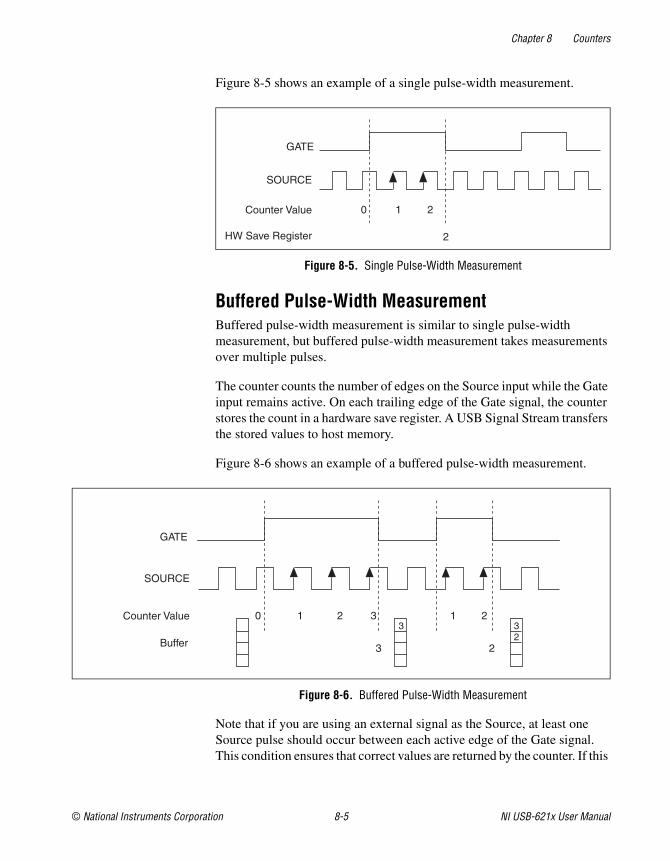
Chapter 8 Counters
© National Instruments Corporation 8-5 NI USB-621x User Manual
Figure 8-5 shows an example of a single pulse-width measurement.
Figure 8-5. Single Pulse-Width Measurement
Buffered Pulse-Width MeasurementBuffered pulse-width measurement is similar to single pulse-width measurement, but buffered pulse-width measurement takes measurements over multiple pulses.
The counter counts the number of edges on the Source input while the Gate input remains active. On each trailing edge of the Gate signal, the counter stores the count in a hardware save register. A USB Signal Stream transfers the stored values to host memory.
Figure 8-6 shows an example of a buffered pulse-width measurement.
Figure 8-6. Buffered Pulse-Width Measurement
Note that if you are using an external signal as the Source, at least one Source pulse should occur between each active edge of the Gate signal. This condition ensures that correct values are returned by the counter. If this
SOURCE
GATE
Counter Value
HW Save Register
1 0
2
2
SOURCE
GATE
Counter Value
Buffer
1 0 3
3 2
2 1 2 3 3
2
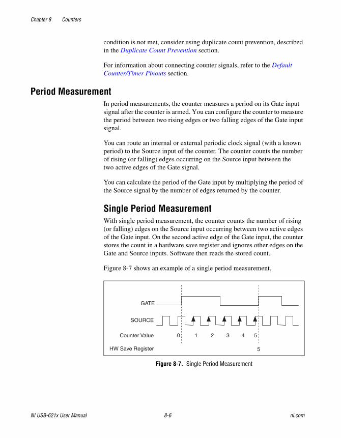
Chapter 8 Counters
NI USB-621x User Manual 8-6 ni.com
condition is not met, consider using duplicate count prevention, described in the Duplicate Count Prevention section.
For information about connecting counter signals, refer to the Default Counter/Timer Pinouts section.
Period MeasurementIn period measurements, the counter measures a period on its Gate input signal after the counter is armed. You can configure the counter to measure the period between two rising edges or two falling edges of the Gate input signal.
You can route an internal or external periodic clock signal (with a known period) to the Source input of the counter. The counter counts the number of rising (or falling) edges occurring on the Source input between the two active edges of the Gate signal.
You can calculate the period of the Gate input by multiplying the period of the Source signal by the number of edges returned by the counter.
Single Period MeasurementWith single period measurement, the counter counts the number of rising (or falling) edges on the Source input occurring between two active edges of the Gate input. On the second active edge of the Gate input, the counter stores the count in a hardware save register and ignores other edges on the Gate and Source inputs. Software then reads the stored count.
Figure 8-7 shows an example of a single period measurement.
Figure 8-7. Single Period Measurement
SOURCE
GATE
Counter Value
HW Save Register
1 0 3
5
4 5 2
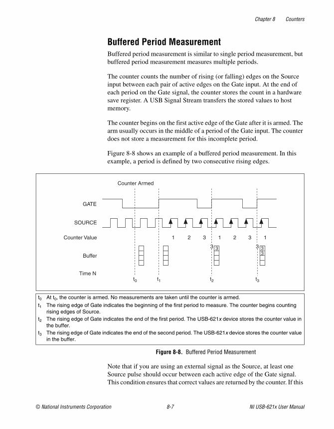
Chapter 8 Counters
© National Instruments Corporation 8-7 NI USB-621x User Manual
Buffered Period MeasurementBuffered period measurement is similar to single period measurement, but buffered period measurement measures multiple periods.
The counter counts the number of rising (or falling) edges on the Source input between each pair of active edges on the Gate input. At the end of each period on the Gate signal, the counter stores the count in a hardware save register. A USB Signal Stream transfers the stored values to host memory.
The counter begins on the first active edge of the Gate after it is armed. The arm usually occurs in the middle of a period of the Gate input. The counter does not store a measurement for this incomplete period.
Figure 8-8 shows an example of a buffered period measurement. In this example, a period is defined by two consecutive rising edges.
Figure 8-8. Buffered Period Measurement
Note that if you are using an external signal as the Source, at least one Source pulse should occur between each active edge of the Gate signal. This condition ensures that correct values are returned by the counter. If this
t0 At t0, the counter is armed. No measurements are taken until the counter is armed.
t1 The rising edge of Gate indicates the beginning of the first period to measure. The counter begins counting rising edges of Source.
t2 The rising edge of Gate indicates the end of the first period. The USB-621x device stores the counter value in the buffer.
t3 The rising edge of Gate indicates the end of the second period. The USB-621x device stores the counter value in the buffer.
SOURCE
GATE
Counter Value
Buffer
1 3
3
31 12 2
33
3
Counter Armed
Time N
3
t0 t1 t2 t3
Chapter 8 Counters
NI USB-621x User Manual 8-8 ni.com
condition is not met, the counter returns a zero. Refer to the Duplicate Count Prevention section for more information.
For information about connecting counter signals, refer to the Default Counter/Timer Pinouts section.
Semi-Period MeasurementIn semi-period measurements, the counter measures a semi-period on its Gate input signal after the counter is armed. A semi-period is the time between any two consecutive edges on the Gate input.
You can route an internal or external periodic clock signal (with a known period) to the Source input of the counter. The counter counts the number of rising (or falling) edges occurring on the Source input between two edges of the Gate signal.
You can calculate the semi-period of the Gate input by multiplying the period of the Source signal by the number of edges returned by the counter.
Single Semi-Period MeasurementSingle semi-period measurement is equivalent to single pulse-width measurement.
Buffered Semi-Period MeasurementIn buffered semi-period measurement, on each edge of the Gate signal, the counter stores the count in a hardware save register. A USB Signal Stream transfers the stored values to host memory.
The counter begins counting on the first active edge of the Gate after it is armed. The arm usually occurs between edges on the Gate input. The counter does not store a value for this incomplete semi-period.
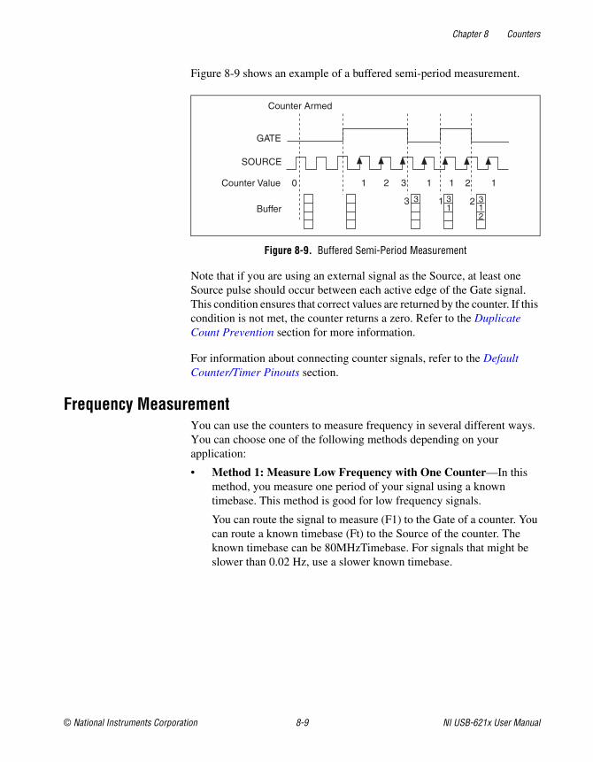
Chapter 8 Counters
© National Instruments Corporation 8-9 NI USB-621x User Manual
Figure 8-9 shows an example of a buffered semi-period measurement.
Figure 8-9. Buffered Semi-Period Measurement
Note that if you are using an external signal as the Source, at least one Source pulse should occur between each active edge of the Gate signal. This condition ensures that correct values are returned by the counter. If this condition is not met, the counter returns a zero. Refer to the Duplicate Count Prevention section for more information.
For information about connecting counter signals, refer to the Default Counter/Timer Pinouts section.
Frequency MeasurementYou can use the counters to measure frequency in several different ways. You can choose one of the following methods depending on your application:
• Method 1: Measure Low Frequency with One Counter—In this method, you measure one period of your signal using a known timebase. This method is good for low frequency signals.
You can route the signal to measure (F1) to the Gate of a counter. You can route a known timebase (Ft) to the Source of the counter. The known timebase can be 80MHzTimebase. For signals that might be slower than 0.02 Hz, use a slower known timebase.
312
31
3
SOURCE
GATE
Counter Value
Buffer
1 3
2
2 1 1
1 3
1 2 0
Counter Armed
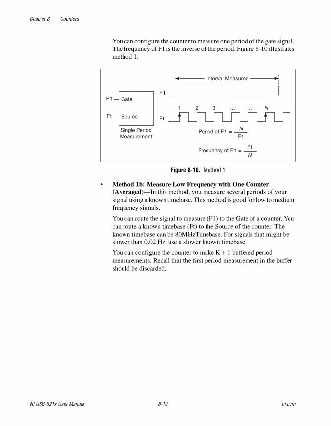
Chapter 8 Counters
NI USB-621x User Manual 8-10 ni.com
You can configure the counter to measure one period of the gate signal. The frequency of F1 is the inverse of the period. Figure 8-10 illustrates method 1.
Figure 8-10. Method 1
• Method 1b: Measure Low Frequency with One Counter (Averaged)—In this method, you measure several periods of your signal using a known timebase. This method is good for low to medium frequency signals.
You can route the signal to measure (F1) to the Gate of a counter. You can route a known timebase (Ft) to the Source of the counter. The known timebase can be 80MHzTimebase. For signals that might be slower than 0.02 Hz, use a slower known timebase.
You can configure the counter to make K + 1 buffered period measurements. Recall that the first period measurement in the buffer should be discarded.
F1
Ft
F1
Ft
Gate
Source
1 2 3 … N
Single PeriodMeasurement
…
Period of F1 = N
Ft
Frequency of F1 =N
Ft
Interval Measured
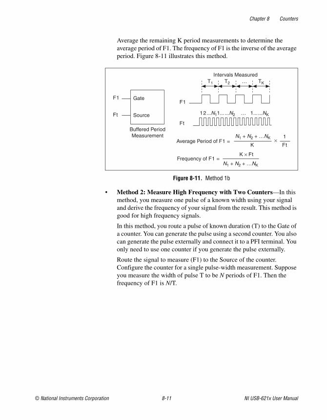
Chapter 8 Counters
© National Instruments Corporation 8-11 NI USB-621x User Manual
Average the remaining K period measurements to determine the average period of F1. The frequency of F1 is the inverse of the average period. Figure 8-11 illustrates this method.
Figure 8-11. Method 1b
• Method 2: Measure High Frequency with Two Counters—In this method, you measure one pulse of a known width using your signal and derive the frequency of your signal from the result. This method is good for high frequency signals.
In this method, you route a pulse of known duration (T) to the Gate of a counter. You can generate the pulse using a second counter. You also can generate the pulse externally and connect it to a PFI terminal. You only need to use one counter if you generate the pulse externally.
Route the signal to measure (F1) to the Source of the counter. Configure the counter for a single pulse-width measurement. Suppose you measure the width of pulse T to be N periods of F1. Then the frequency of F1 is N/T.
F1
Ft
F1
Intervals Measured
Gate
Source
Buffered PeriodMeasurement
Average Period of F1 =N1 + N2 + …NK
K
Frequency of F1 =N1 + N2 + …NK
K × Ft
Ft
T1 T2 … TK
1
Ft ×
1 2 ...N11... ...N2 … 1... ...NK
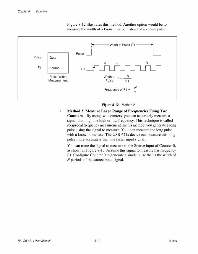
Chapter 8 Counters
NI USB-621x User Manual 8-12 ni.com
Figure 8-12 illustrates this method. Another option would be to measure the width of a known period instead of a known pulse.
Figure 8-12. Method 2
• Method 3: Measure Large Range of Frequencies Using Two Counters—By using two counters, you can accurately measure a signal that might be high or low frequency. This technique is called reciprocal frequency measurement. In this method, you generate a long pulse using the signal to measure. You then measure the long pulse with a known timebase. The USB-621x device can measure this long pulse more accurately than the faster input signal.
You can route the signal to measure to the Source input of Counter 0, as shown in Figure 8-13. Assume this signal to measure has frequency F1. Configure Counter 0 to generate a single pulse that is the width of N periods of the source input signal.
Pulse
F1
Pulse
F1
Gate
Source
1 2 … N
Pulse-Width Measurement
T = N
F1
Frequency of F1 =T
Width of Pulse
N
Width of Pulse (T)
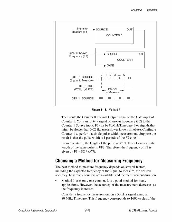
Chapter 8 Counters
© National Instruments Corporation 8-13 NI USB-621x User Manual
Figure 8-13. Method 3
Then route the Counter 0 Internal Output signal to the Gate input of Counter 1. You can route a signal of known frequency (F2) to the Counter 1 Source input. F2 can be 80MHzTimebase. For signals that might be slower than 0.02 Hz, use a slower known timebase. Configure Counter 1 to perform a single pulse-width measurement. Suppose the result is that the pulse width is J periods of the F2 clock.
From Counter 0, the length of the pulse is N/F1. From Counter 1, the length of the same pulse is J/F2. Therefore, the frequency of F1 is given by F1 = F2 * (N/J).
Choosing a Method for Measuring FrequencyThe best method to measure frequency depends on several factors including the expected frequency of the signal to measure, the desired accuracy, how many counters are available, and the measurement duration.
• Method 1 uses only one counter. It is a good method for many applications. However, the accuracy of the measurement decreases as the frequency increases.
Consider a frequency measurement on a 50 kHz signal using an 80 MHz Timebase. This frequency corresponds to 1600 cycles of the
SOURCE OUT
COUNTER 0
SOURCE
GATE
OUT
COUNTER 1
Signal to Measure (F1)
Signal of Known Frequency (F2)
CTR_0_SOURCE (Signal to Measure)
CTR_0_OUT (CTR_1_GATE)
CTR_1_SOURCE
Interval to Measure
0 1 2 3 … N
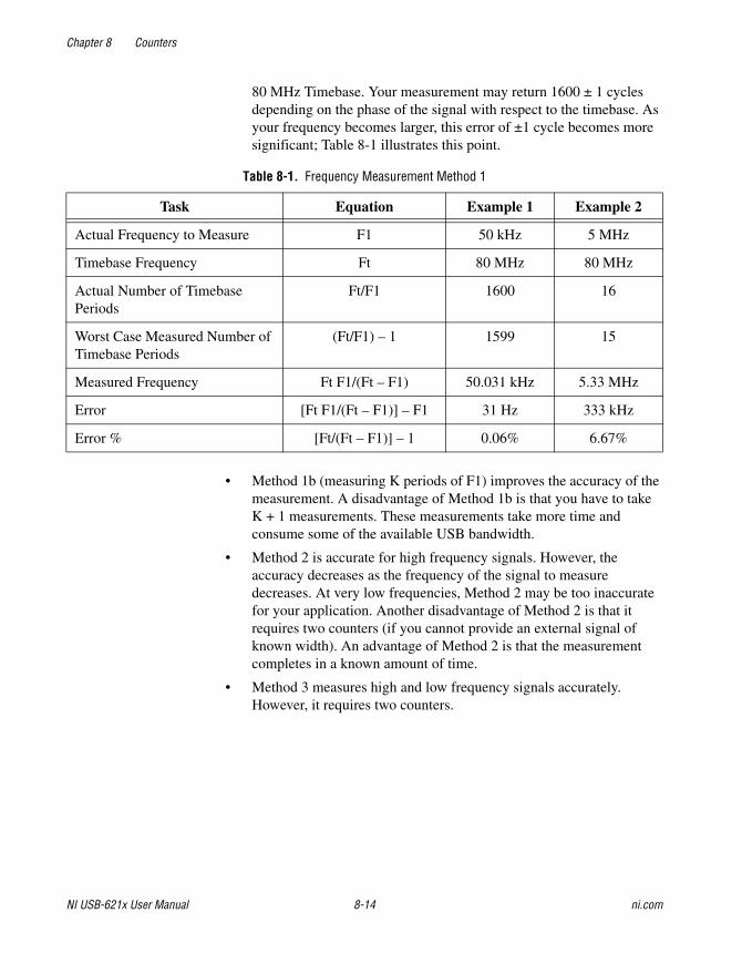
Chapter 8 Counters
NI USB-621x User Manual 8-14 ni.com
80 MHz Timebase. Your measurement may return 1600 ± 1 cycles depending on the phase of the signal with respect to the timebase. As your frequency becomes larger, this error of ±1 cycle becomes more significant; Table 8-1 illustrates this point.
• Method 1b (measuring K periods of F1) improves the accuracy of the measurement. A disadvantage of Method 1b is that you have to take K + 1 measurements. These measurements take more time and consume some of the available USB bandwidth.
• Method 2 is accurate for high frequency signals. However, the accuracy decreases as the frequency of the signal to measure decreases. At very low frequencies, Method 2 may be too inaccurate for your application. Another disadvantage of Method 2 is that it requires two counters (if you cannot provide an external signal of known width). An advantage of Method 2 is that the measurement completes in a known amount of time.
• Method 3 measures high and low frequency signals accurately. However, it requires two counters.
Table 8-1. Frequency Measurement Method 1
Task Equation Example 1 Example 2
Actual Frequency to Measure F1 50 kHz 5 MHz
Timebase Frequency Ft 80 MHz 80 MHz
Actual Number of Timebase Periods
Ft/F1 1600 16
Worst Case Measured Number of Timebase Periods
(Ft/F1) – 1 1599 15
Measured Frequency Ft F1/(Ft – F1) 50.031 kHz 5.33 MHz
Error [Ft F1/(Ft – F1)] – F1 31 Hz 333 kHz
Error % [Ft/(Ft – F1)] – 1 0.06% 6.67%
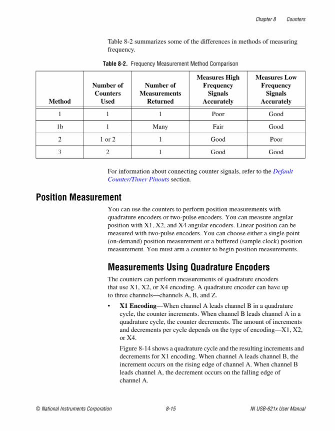
Chapter 8 Counters
© National Instruments Corporation 8-15 NI USB-621x User Manual
Table 8-2 summarizes some of the differences in methods of measuring frequency.
For information about connecting counter signals, refer to the Default Counter/Timer Pinouts section.
Position MeasurementYou can use the counters to perform position measurements with quadrature encoders or two-pulse encoders. You can measure angular position with X1, X2, and X4 angular encoders. Linear position can be measured with two-pulse encoders. You can choose either a single point (on-demand) position measurement or a buffered (sample clock) position measurement. You must arm a counter to begin position measurements.
Measurements Using Quadrature EncodersThe counters can perform measurements of quadrature encoders that use X1, X2, or X4 encoding. A quadrature encoder can have up to three channels—channels A, B, and Z.
• X1 Encoding—When channel A leads channel B in a quadrature cycle, the counter increments. When channel B leads channel A in a quadrature cycle, the counter decrements. The amount of increments and decrements per cycle depends on the type of encoding—X1, X2, or X4.
Figure 8-14 shows a quadrature cycle and the resulting increments and decrements for X1 encoding. When channel A leads channel B, the increment occurs on the rising edge of channel A. When channel B leads channel A, the decrement occurs on the falling edge of channel A.
Table 8-2. Frequency Measurement Method Comparison
Method
Number of Counters
Used
Number of Measurements
Returned
Measures High Frequency
Signals Accurately
Measures Low Frequency
Signals Accurately
1 1 1 Poor Good
1b 1 Many Fair Good
2 1 or 2 1 Good Poor
3 2 1 Good Good
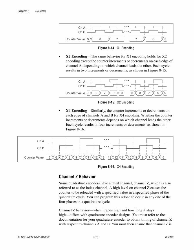
Chapter 8 Counters
NI USB-621x User Manual 8-16 ni.com
Figure 8-14. X1 Encoding
• X2 Encoding—The same behavior for X1 encoding holds for X2 encoding except the counter increments or decrements on each edge of channel A, depending on which channel leads the other. Each cycle results in two increments or decrements, as shown in Figure 8-15.
Figure 8-15. X2 Encoding
• X4 Encoding—Similarly, the counter increments or decrements on each edge of channels A and B for X4 encoding. Whether the counter increments or decrements depends on which channel leads the other. Each cycle results in four increments or decrements, as shown in Figure 8-16.
Figure 8-16. X4 Encoding
Channel Z BehaviorSome quadrature encoders have a third channel, channel Z, which is also referred to as the index channel. A high level on channel Z causes the counter to be reloaded with a specified value in a specified phase of the quadrature cycle. You can program this reload to occur in any one of the four phases in a quadrature cycle.
Channel Z behavior—when it goes high and how long it stays high—differs with quadrature encoder designs. You must refer to the documentation for your quadrature encoder to obtain timing of channel Z with respect to channels A and B. You must then ensure that channel Z is
Ch A Ch B
Counter Value 7 7 6 5 5 6
Ch ACh B
Counter Value 5 6 8 97 5689 7
Ch A
Ch B
Counter Value 5 6 8 9 10 10 11 11 12 12 13 13 7 5 6 8 7 9
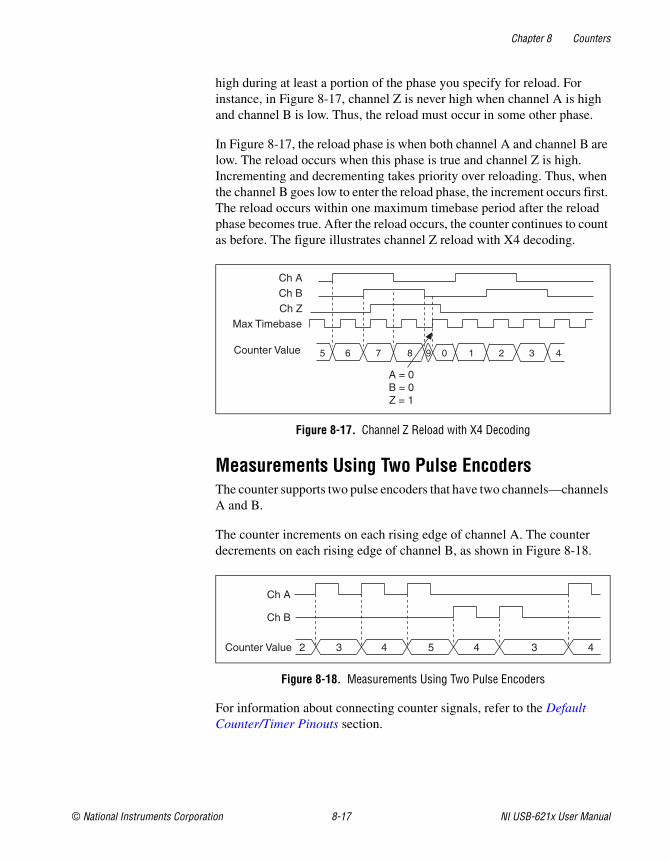
Chapter 8 Counters
© National Instruments Corporation 8-17 NI USB-621x User Manual
high during at least a portion of the phase you specify for reload. For instance, in Figure 8-17, channel Z is never high when channel A is high and channel B is low. Thus, the reload must occur in some other phase.
In Figure 8-17, the reload phase is when both channel A and channel B are low. The reload occurs when this phase is true and channel Z is high. Incrementing and decrementing takes priority over reloading. Thus, when the channel B goes low to enter the reload phase, the increment occurs first. The reload occurs within one maximum timebase period after the reload phase becomes true. After the reload occurs, the counter continues to count as before. The figure illustrates channel Z reload with X4 decoding.
Figure 8-17. Channel Z Reload with X4 Decoding
Measurements Using Two Pulse EncodersThe counter supports two pulse encoders that have two channels—channels A and B.
The counter increments on each rising edge of channel A. The counter decrements on each rising edge of channel B, as shown in Figure 8-18.
Figure 8-18. Measurements Using Two Pulse Encoders
For information about connecting counter signals, refer to the Default Counter/Timer Pinouts section.
Ch A Ch B
Counter Value 5 6
A = 0 B = 0 Z = 1
Ch Z Max Timebase
8 9 0 2 1 7 4 3
Ch A
Ch B
Counter Value 2 3 5 4 3 4 4
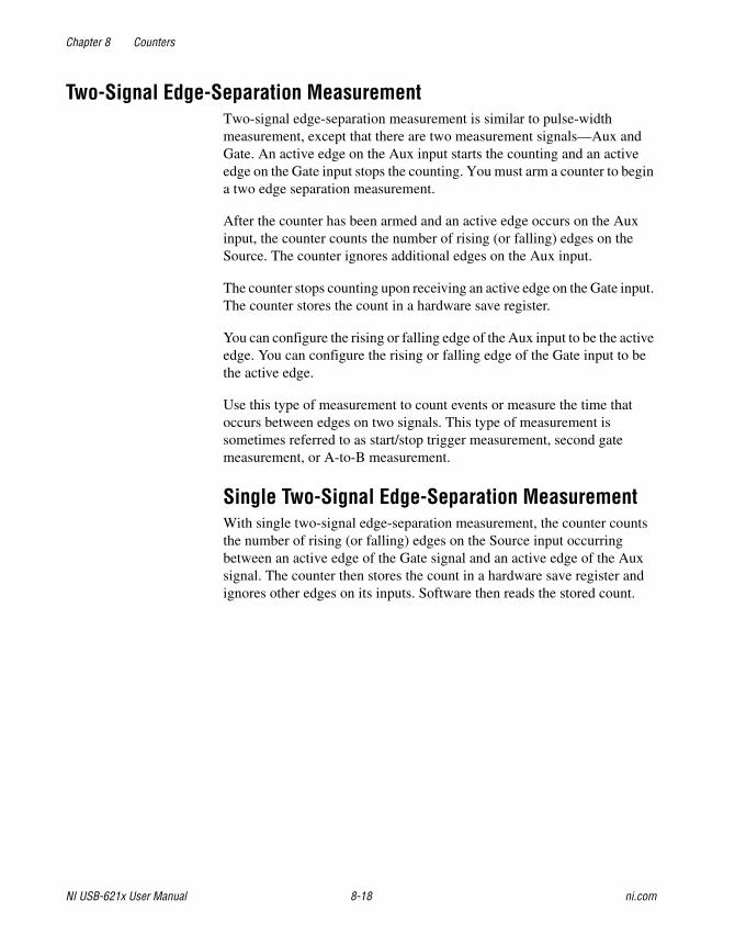
Chapter 8 Counters
NI USB-621x User Manual 8-18 ni.com
Two-Signal Edge-Separation MeasurementTwo-signal edge-separation measurement is similar to pulse-width measurement, except that there are two measurement signals—Aux and Gate. An active edge on the Aux input starts the counting and an active edge on the Gate input stops the counting. You must arm a counter to begin a two edge separation measurement.
After the counter has been armed and an active edge occurs on the Aux input, the counter counts the number of rising (or falling) edges on the Source. The counter ignores additional edges on the Aux input.
The counter stops counting upon receiving an active edge on the Gate input. The counter stores the count in a hardware save register.
You can configure the rising or falling edge of the Aux input to be the active edge. You can configure the rising or falling edge of the Gate input to be the active edge.
Use this type of measurement to count events or measure the time that occurs between edges on two signals. This type of measurement is sometimes referred to as start/stop trigger measurement, second gate measurement, or A-to-B measurement.
Single Two-Signal Edge-Separation MeasurementWith single two-signal edge-separation measurement, the counter counts the number of rising (or falling) edges on the Source input occurring between an active edge of the Gate signal and an active edge of the Aux signal. The counter then stores the count in a hardware save register and ignores other edges on its inputs. Software then reads the stored count.
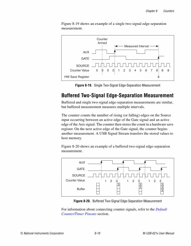
Chapter 8 Counters
© National Instruments Corporation 8-19 NI USB-621x User Manual
Figure 8-19 shows an example of a single two-signal edge-separation measurement.
Figure 8-19. Single Two-Signal Edge-Separation Measurement
Buffered Two-Signal Edge-Separation MeasurementBuffered and single two-signal edge-separation measurements are similar, but buffered measurement measures multiple intervals.
The counter counts the number of rising (or falling) edges on the Source input occurring between an active edge of the Gate signal and an active edge of the Aux signal. The counter then stores the count in a hardware save register. On the next active edge of the Gate signal, the counter begins another measurement. A USB Signal Stream transfers the stored values to host memory.
Figure 8-20 shows an example of a buffered two-signal edge-separation measurement.
Figure 8-20. Buffered Two-Signal Edge-Separation Measurement
For information about connecting counter signals, refer to the Default Counter/Timer Pinouts section.
AUX
Counter Armed
8
0 0 0 0 1 2 3 4 5 6 7 8 8 8
Measured Interval
GATE
SOURCE
Counter Value
HW Save Register
SOURCE
Counter Value
Buffer
AUX
GATE
1 2 3 1 2 3 1 2 3 3 3
3 3 3 3
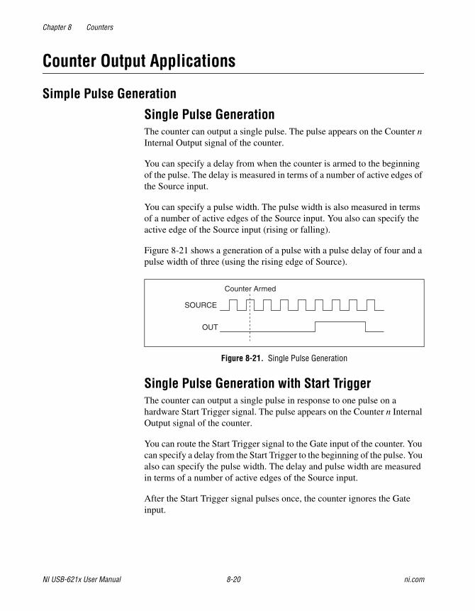
Chapter 8 Counters
NI USB-621x User Manual 8-20 ni.com
Counter Output Applications
Simple Pulse Generation
Single Pulse GenerationThe counter can output a single pulse. The pulse appears on the Counter n Internal Output signal of the counter.
You can specify a delay from when the counter is armed to the beginning of the pulse. The delay is measured in terms of a number of active edges of the Source input.
You can specify a pulse width. The pulse width is also measured in terms of a number of active edges of the Source input. You also can specify the active edge of the Source input (rising or falling).
Figure 8-21 shows a generation of a pulse with a pulse delay of four and a pulse width of three (using the rising edge of Source).
Figure 8-21. Single Pulse Generation
Single Pulse Generation with Start TriggerThe counter can output a single pulse in response to one pulse on a hardware Start Trigger signal. The pulse appears on the Counter n Internal Output signal of the counter.
You can route the Start Trigger signal to the Gate input of the counter. You can specify a delay from the Start Trigger to the beginning of the pulse. You also can specify the pulse width. The delay and pulse width are measured in terms of a number of active edges of the Source input.
After the Start Trigger signal pulses once, the counter ignores the Gate input.
SOURCE
OUT
Counter Armed
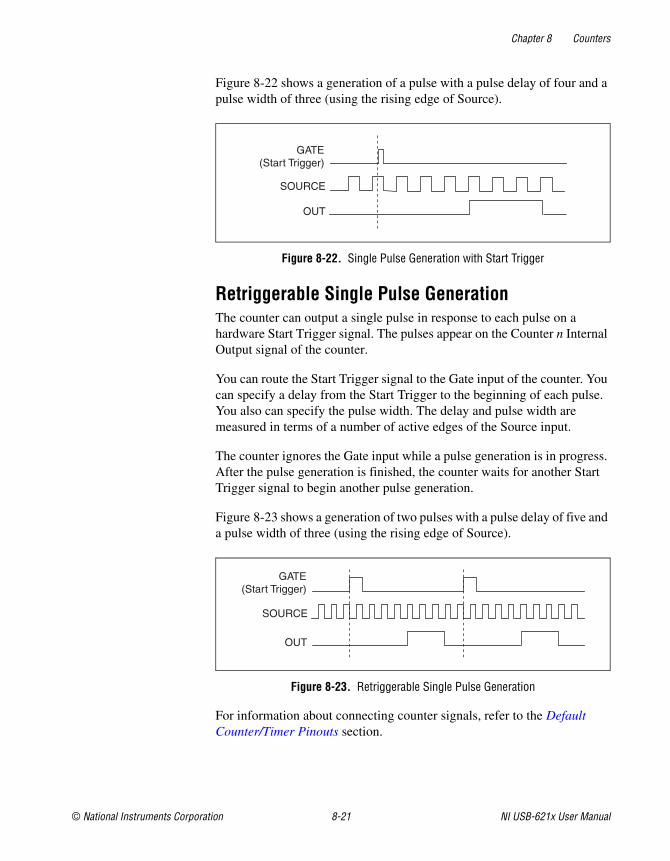
Chapter 8 Counters
© National Instruments Corporation 8-21 NI USB-621x User Manual
Figure 8-22 shows a generation of a pulse with a pulse delay of four and a pulse width of three (using the rising edge of Source).
Figure 8-22. Single Pulse Generation with Start Trigger
Retriggerable Single Pulse GenerationThe counter can output a single pulse in response to each pulse on a hardware Start Trigger signal. The pulses appear on the Counter n Internal Output signal of the counter.
You can route the Start Trigger signal to the Gate input of the counter. You can specify a delay from the Start Trigger to the beginning of each pulse. You also can specify the pulse width. The delay and pulse width are measured in terms of a number of active edges of the Source input.
The counter ignores the Gate input while a pulse generation is in progress. After the pulse generation is finished, the counter waits for another Start Trigger signal to begin another pulse generation.
Figure 8-23 shows a generation of two pulses with a pulse delay of five and a pulse width of three (using the rising edge of Source).
Figure 8-23. Retriggerable Single Pulse Generation
For information about connecting counter signals, refer to the Default Counter/Timer Pinouts section.
SOURCE
GATE (Start Trigger)
OUT
SOURCE
GATE (Start Trigger)
OUT
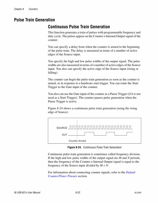
Chapter 8 Counters
NI USB-621x User Manual 8-22 ni.com
Pulse Train Generation
Continuous Pulse Train GenerationThis function generates a train of pulses with programmable frequency and duty cycle. The pulses appear on the Counter n Internal Output signal of the counter.
You can specify a delay from when the counter is armed to the beginning of the pulse train. The delay is measured in terms of a number of active edges of the Source input.
You specify the high and low pulse widths of the output signal. The pulse widths are also measured in terms of a number of active edges of the Source input. You also can specify the active edge of the Source input (rising or falling).
The counter can begin the pulse train generation as soon as the counter is armed, or in response to a hardware start trigger. You can route the Start Trigger to the Gate input of the counter.
You also can use the Gate input of the counter as a Pause Trigger (if it is not used as a Start Trigger). The counter pauses pulse generation when the Pause Trigger is active.
Figure 8-24 shows a continuous pulse train generation (using the rising edge of Source).
Figure 8-24. Continuous Pulse Train Generation
Continuous pulse train generation is sometimes called frequency division. If the high and low pulse widths of the output signal are M and N periods, then the frequency of the Counter n Internal Output signal is equal to the frequency of the Source input divided by M + N.
For information about connecting counter signals, refer to the Default Counter/Timer Pinouts section.
SOURCE
OUT
Counter Armed
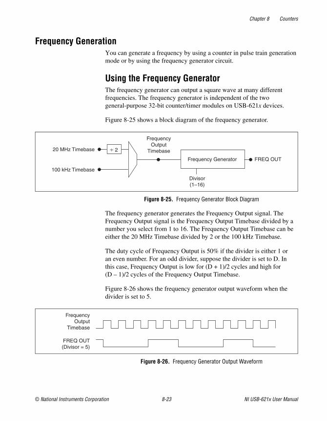
Chapter 8 Counters
© National Instruments Corporation 8-23 NI USB-621x User Manual
Frequency GenerationYou can generate a frequency by using a counter in pulse train generation mode or by using the frequency generator circuit.
Using the Frequency GeneratorThe frequency generator can output a square wave at many different frequencies. The frequency generator is independent of the two general-purpose 32-bit counter/timer modules on USB-621x devices.
Figure 8-25 shows a block diagram of the frequency generator.
Figure 8-25. Frequency Generator Block Diagram
The frequency generator generates the Frequency Output signal. The Frequency Output signal is the Frequency Output Timebase divided by a number you select from 1 to 16. The Frequency Output Timebase can be either the 20 MHz Timebase divided by 2 or the 100 kHz Timebase.
The duty cycle of Frequency Output is 50% if the divider is either 1 or an even number. For an odd divider, suppose the divider is set to D. In this case, Frequency Output is low for (D + 1)/2 cycles and high for (D – 1)/2 cycles of the Frequency Output Timebase.
Figure 8-26 shows the frequency generator output waveform when the divider is set to 5.
Figure 8-26. Frequency Generator Output Waveform
100 kHz Timebase
20 MHz Timebase
FrequencyOutput
Timebase
FREQ OUT
Divisor(1–16)
Frequency Generator
÷ 2
FrequencyOutput
Timebase
FREQ OUT(Divisor = 5)
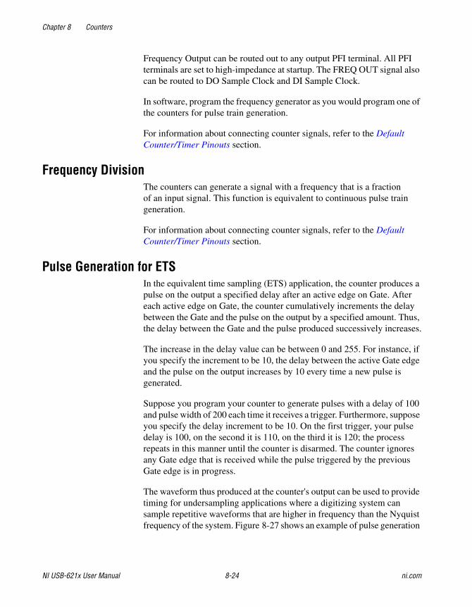
Chapter 8 Counters
NI USB-621x User Manual 8-24 ni.com
Frequency Output can be routed out to any output PFI terminal. All PFI terminals are set to high-impedance at startup. The FREQ OUT signal also can be routed to DO Sample Clock and DI Sample Clock.
In software, program the frequency generator as you would program one of the counters for pulse train generation.
For information about connecting counter signals, refer to the Default Counter/Timer Pinouts section.
Frequency DivisionThe counters can generate a signal with a frequency that is a fraction of an input signal. This function is equivalent to continuous pulse train generation.
For information about connecting counter signals, refer to the Default Counter/Timer Pinouts section.
Pulse Generation for ETSIn the equivalent time sampling (ETS) application, the counter produces a pulse on the output a specified delay after an active edge on Gate. After each active edge on Gate, the counter cumulatively increments the delay between the Gate and the pulse on the output by a specified amount. Thus, the delay between the Gate and the pulse produced successively increases.
The increase in the delay value can be between 0 and 255. For instance, if you specify the increment to be 10, the delay between the active Gate edge and the pulse on the output increases by 10 every time a new pulse is generated.
Suppose you program your counter to generate pulses with a delay of 100 and pulse width of 200 each time it receives a trigger. Furthermore, suppose you specify the delay increment to be 10. On the first trigger, your pulse delay is 100, on the second it is 110, on the third it is 120; the process repeats in this manner until the counter is disarmed. The counter ignores any Gate edge that is received while the pulse triggered by the previous Gate edge is in progress.
The waveform thus produced at the counter's output can be used to provide timing for undersampling applications where a digitizing system can sample repetitive waveforms that are higher in frequency than the Nyquist frequency of the system. Figure 8-27 shows an example of pulse generation
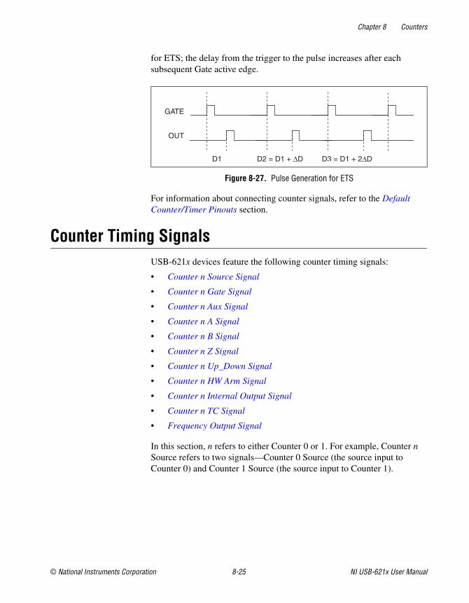
Chapter 8 Counters
© National Instruments Corporation 8-25 NI USB-621x User Manual
for ETS; the delay from the trigger to the pulse increases after each subsequent Gate active edge.
Figure 8-27. Pulse Generation for ETS
For information about connecting counter signals, refer to the Default Counter/Timer Pinouts section.
Counter Timing SignalsUSB-621x devices feature the following counter timing signals:
• Counter n Source Signal
• Counter n Gate Signal
• Counter n Aux Signal
• Counter n A Signal
• Counter n B Signal
• Counter n Z Signal
• Counter n Up_Down Signal
• Counter n HW Arm Signal
• Counter n Internal Output Signal
• Counter n TC Signal
• Frequency Output Signal
In this section, n refers to either Counter 0 or 1. For example, Counter n Source refers to two signals—Counter 0 Source (the source input to Counter 0) and Counter 1 Source (the source input to Counter 1).
OUT
D1 D2 = D1 + ΔD D3 = D1 + 2ΔD
GATE
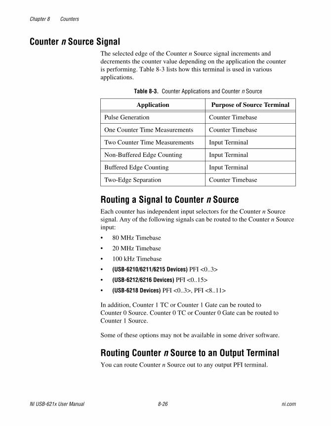
Chapter 8 Counters
NI USB-621x User Manual 8-26 ni.com
Counter n Source SignalThe selected edge of the Counter n Source signal increments and decrements the counter value depending on the application the counter is performing. Table 8-3 lists how this terminal is used in various applications.
Routing a Signal to Counter n SourceEach counter has independent input selectors for the Counter n Source signal. Any of the following signals can be routed to the Counter n Source input:
• 80 MHz Timebase
• 20 MHz Timebase
• 100 kHz Timebase
• (USB-6210/6211/6215 Devices) PFI <0..3>
• (USB-6212/6216 Devices) PFI <0..15>
• (USB-6218 Devices) PFI <0..3>, PFI <8..11>
In addition, Counter 1 TC or Counter 1 Gate can be routed to Counter 0 Source. Counter 0 TC or Counter 0 Gate can be routed to Counter 1 Source.
Some of these options may not be available in some driver software.
Routing Counter n Source to an Output TerminalYou can route Counter n Source out to any output PFI terminal.
Table 8-3. Counter Applications and Counter n Source
Application Purpose of Source Terminal
Pulse Generation Counter Timebase
One Counter Time Measurements Counter Timebase
Two Counter Time Measurements Input Terminal
Non-Buffered Edge Counting Input Terminal
Buffered Edge Counting Input Terminal
Two-Edge Separation Counter Timebase
Chapter 8 Counters
© National Instruments Corporation 8-27 NI USB-621x User Manual
Counter n Gate SignalThe Counter n Gate signal can perform many different operations depending on the application including starting and stopping the counter, and saving the counter contents.
Routing a Signal to Counter n GateEach counter has independent input selectors for the Counter n Gate signal. Any of the following signals can be routed to the Counter n Gate input:
• (USB-6210/6211/6215 Devices) PFI <0..3>
• (USB-6212/6216 Devices) PFI <0..15>
• (USB-6218 Devices) PFI <0..3>, PFI <8..11>
• AI Reference Trigger (ai/ReferenceTrigger)
• AI Start Trigger (ai/StartTrigger)
• AI Sample Clock (ai/SampleClock)
• AI Convert Clock (ai/ConvertClock)
• AO Sample Clock (ao/SampleClock)
In addition, Counter 1 Internal Output or Counter 1 Source can be routed to Counter 0 Gate. Counter 0 Internal Output or Counter 0 Source can be routed to Counter 1 Gate.
Some of these options may not be available in some driver software.
Routing Counter n Gate to an Output TerminalYou can route Counter n Gate out to any output PFI terminal.
Counter n Aux SignalThe Counter n Aux signal indicates the first edge in a two-signal edge-separation measurement.
Routing a Signal to Counter n AuxEach counter has independent input selectors for the Counter n Aux signal. Any of the following signals can be routed to the Counter n Aux input:
• (USB-6210/6211/6215 Devices) PFI <0..3>
• (USB-6212/6216 Devices) PFI <0..15>
• (USB-6218 Devices) PFI <0..3>, PFI <8..11>
Chapter 8 Counters
NI USB-621x User Manual 8-28 ni.com
• AI Reference Trigger (ai/ReferenceTrigger)
• AI Start Trigger (ai/StartTrigger)
In addition, Counter 1 Internal Output, Counter 1 Gate, Counter 1 Source, or Counter 0 Gate can be routed to Counter 0 Aux. Counter 0 Internal Output, Counter 0 Gate, Counter 0 Source, or Counter 1 Gate can be routed to Counter 1 Aux.
Some of these options may not be available in some driver software.
Counter n A, Counter n B, and Counter n Z SignalsCounter n B can control the direction of counting in edge counting applications. Use the A, B, and Z inputs to each counter when measuring quadrature encoders or measuring two pulse encoders.
Routing Signals to A, B, and Z Counter InputsEach counter has independent input selectors for each of the A, B, and Z inputs. You can route any input PFI signal to each input.
Counter n Up_Down SignalCounter n Up_Down is another name for the Counter n B signal.
Counter n HW Arm SignalThe Counter n HW Arm signal enables a counter to begin an input or output function.
To begin any counter input or output function, you must first enable, or arm, the counter. In some applications, such as buffered semi-period measurement, the counter begins counting when it is armed. In other applications, such as single pulse-width measurement, the counter begins waiting for the Gate signal when it is armed. Counter output operations can use the arm signal in addition to a start trigger.
Software can arm a counter or configure counters to be armed on a hardware signal. Software calls this hardware signal the Arm Start Trigger. Internally, software routes the Arm Start Trigger to the Counter n HW Arm input of the counter.
Chapter 8 Counters
© National Instruments Corporation 8-29 NI USB-621x User Manual
Routing Signals to Counter n HW Arm InputAny of the following signals can be routed to the Counter n HW Arm input:
• (USB-6210/6211/6215 Devices) PFI <0..3>
• (USB-6212/6216 Devices) PFI <0..15>
• (USB-6218 Devices) PFI <0..3>, PFI <8..11>
• AI Reference Trigger (ai/ReferenceTrigger)
• AI Start Trigger (ai/StartTrigger)
Counter 1 Internal Output can be routed to Counter 0 HW Arm. Counter 0 Internal Output can be routed to Counter 1 HW Arm.
Some of these options may not be available in some driver software.
Counter n Internal Output and Counter n TC SignalsThe Counter n Internal Output signal changes in response to Counter n TC.
The two software-selectable output options are pulse output on TC and toggle output on TC. The output polarity is software-selectable for both options.
With pulse or pulse train generation tasks, the counter drives the pulse(s) on the Counter n Internal Output signal. The Counter n Internal Output signal can be internally routed to be a counter/timer input or an “external” source for AI, AO, DI, or DO timing signals.
Routing Counter n Internal Output to an Output TerminalYou can route Counter n Internal Output to any output PFI terminal.
Frequency Output SignalThe Frequency Output (FREQ OUT) signal is the output of the frequency output generator.
Routing Frequency Output to a TerminalYou can route Frequency Output to any output PFI terminal.
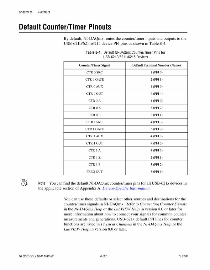
Chapter 8 Counters
NI USB-621x User Manual 8-30 ni.com
Default Counter/Timer PinoutsBy default, NI-DAQmx routes the counter/timer inputs and outputs to the USB-6210/6211/6215 device PFI pins as shown in Table 8-4.
Note You can find the default NI-DAQmx counter/timer pins for all USB-621x devices in the applicable section of Appendix A, Device-Specific Information.
You can use these defaults or select other sources and destinations for the counter/timer signals in NI-DAQmx. Refer to Connecting Counter Signals in the NI-DAQmx Help or the LabVIEW Help in version 8.0 or later for more information about how to connect your signals for common counter measurements and generations. USB-621x default PFI lines for counter functions are listed in Physical Channels in the NI-DAQmx Help or the LabVIEW Help in version 8.0 or later.
Table 8-4. Default NI-DAQmx Counter/Timer Pins for USB-6210/6211/6215 Devices
Counter/Timer Signal Default Terminal Number (Name)
CTR 0 SRC 1 (PFI 0)
CTR 0 GATE 2 (PFI 1)
CTR 0 AUX 1 (PFI 0)
CTR 0 OUT 6 (PFI 4)
CTR 0 A 1 (PFI 0)
CTR 0 Z 3 (PFI 2)
CTR 0 B 2 (PFI 1)
CTR 1 SRC 4 (PFI 3)
CTR 1 GATE 3 (PFI 2)
CTR 1 AUX 4 (PFI 3)
CTR 1 OUT 7 (PFI 5)
CTR 1 A 4 (PFI 3)
CTR 1 Z 2 (PFI 1)
CTR 1 B 3 (PFI 2)
FREQ OUT 8 (PFI 6)
Chapter 8 Counters
© National Instruments Corporation 8-31 NI USB-621x User Manual
Counter TriggeringCounters support three different triggering actions:
• Arm Start Trigger—To begin any counter input or output function, you must first enable, or arm, the counter. Software can arm a counter or configure counters to be armed on a hardware signal. Software calls this hardware signal the Arm Start Trigger. Internally, software routes the Arm Start Trigger to the Counter n HW Arm input of the counter.
For counter output operations, you can use the arm start trigger in addition to the start and pause triggers. For counter input operations, you can use the arm start trigger to have start trigger-like behavior. The arm start trigger can be used for synchronizing multiple counter input and output tasks.
When using an arm start trigger, the arm start trigger source is routed to the Counter n HW Arm signal.
• Start Trigger—For counter output operations, a start trigger can be configured to begin a finite or continuous pulse generation. Once a continuous generation has triggered, the pulses continue to generate until you stop the operation in software. For finite generations, the specified number of pulses is generated and the generation stops unless you use the retriggerable attribute. When you use this attribute, subsequent start triggers cause the generation to restart.
When using a start trigger, the start trigger source is routed to the Counter n Gate signal input of the counter.
Counter input operations can use the arm start trigger to have start trigger-like behavior.
• Pause Trigger—You can use pause triggers in edge counting and continuous pulse generation applications. For edge counting acquisitions, the counter stops counting edges while the external trigger signal is low and resumes when the signal goes high or vice versa. For continuous pulse generations, the counter stops generating pulses while the external trigger signal is low and resumes when the signal goes high or vice versa.
When using a pause trigger, the pause trigger source is routed to the Counter n Gate signal input of the counter.
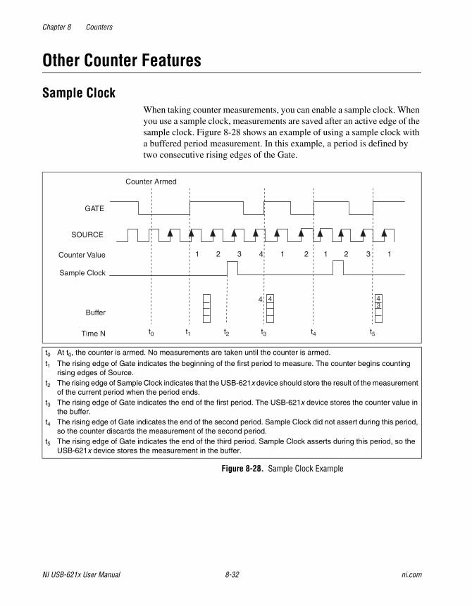
Chapter 8 Counters
NI USB-621x User Manual 8-32 ni.com
Other Counter Features
Sample ClockWhen taking counter measurements, you can enable a sample clock. When you use a sample clock, measurements are saved after an active edge of the sample clock. Figure 8-28 shows an example of using a sample clock with a buffered period measurement. In this example, a period is defined by two consecutive rising edges of the Gate.
Figure 8-28. Sample Clock Example
t0 At t0, the counter is armed. No measurements are taken until the counter is armed.
t1 The rising edge of Gate indicates the beginning of the first period to measure. The counter begins counting rising edges of Source.
t2 The rising edge of Sample Clock indicates that the USB-621x device should store the result of the measurement of the current period when the period ends.
t3 The rising edge of Gate indicates the end of the first period. The USB-621x device stores the counter value in the buffer.
t4 The rising edge of Gate indicates the end of the second period. Sample Clock did not assert during this period, so the counter discards the measurement of the second period.
t5 The rising edge of Gate indicates the end of the third period. Sample Clock asserts during this period, so the USB-621x device stores the measurement in the buffer.
SOURCE
GATE
Buffer
4
Counter Armed
Sample Clock
4 43
Time N
Counter Value
t0 t1 t2 t3 t4 t5
1 2 3 4 1 2 1 2 3 1
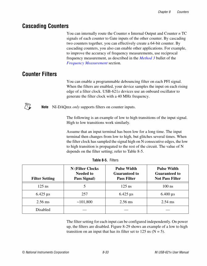
Chapter 8 Counters
© National Instruments Corporation 8-33 NI USB-621x User Manual
Cascading CountersYou can internally route the Counter n Internal Output and Counter n TC signals of each counter to Gate inputs of the other counter. By cascading two counters together, you can effectively create a 64-bit counter. By cascading counters, you also can enable other applications. For example, to improve the accuracy of frequency measurements, use reciprocal frequency measurement, as described in the Method 3 bullet of the Frequency Measurement section.
Counter FiltersYou can enable a programmable debouncing filter on each PFI signal. When the filters are enabled, your device samples the input on each rising edge of a filter clock. USB-621x devices use an onboard oscillator to generate the filter clock with a 40 MHz frequency.
Note NI-DAQmx only supports filters on counter inputs.
The following is an example of low to high transitions of the input signal. High to low transitions work similarly.
Assume that an input terminal has been low for a long time. The input terminal then changes from low to high, but glitches several times. When the filter clock has sampled the signal high on N consecutive edges, the low to high transition is propagated to the rest of the circuit. The value of N depends on the filter setting; refer to Table 8-5.
The filter setting for each input can be configured independently. On power up, the filters are disabled. Figure 8-29 shows an example of a low to high transition on an input that has its filter set to 125 ns (N = 5).
Table 8-5. Filters
Filter Setting
N (Filter Clocks Needed to
Pass Signal)
Pulse Width Guaranteed to
Pass Filter
Pulse Width Guaranteed to Not Pass Filter
125 ns 5 125 ns 100 ns
6.425 μs 257 6.425 μs 6.400 μs
2.56 ms ~101,800 2.56 ms 2.54 ms
Disabled — — —
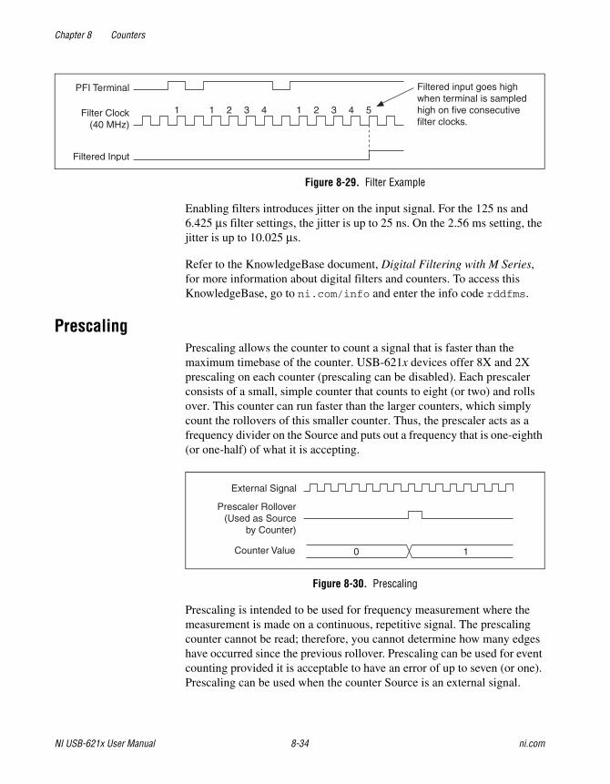
Chapter 8 Counters
NI USB-621x User Manual 8-34 ni.com
Figure 8-29. Filter Example
Enabling filters introduces jitter on the input signal. For the 125 ns and 6.425 μs filter settings, the jitter is up to 25 ns. On the 2.56 ms setting, the jitter is up to 10.025 μs.
Refer to the KnowledgeBase document, Digital Filtering with M Series, for more information about digital filters and counters. To access this KnowledgeBase, go to ni.com/info and enter the info code rddfms.
PrescalingPrescaling allows the counter to count a signal that is faster than the maximum timebase of the counter. USB-621x devices offer 8X and 2X prescaling on each counter (prescaling can be disabled). Each prescaler consists of a small, simple counter that counts to eight (or two) and rolls over. This counter can run faster than the larger counters, which simply count the rollovers of this smaller counter. Thus, the prescaler acts as a frequency divider on the Source and puts out a frequency that is one-eighth (or one-half) of what it is accepting.
Figure 8-30. Prescaling
Prescaling is intended to be used for frequency measurement where the measurement is made on a continuous, repetitive signal. The prescaling counter cannot be read; therefore, you cannot determine how many edges have occurred since the previous rollover. Prescaling can be used for event counting provided it is acceptable to have an error of up to seven (or one). Prescaling can be used when the counter Source is an external signal.
1 2 3 1 4 1 2 3 4 5
PFI Terminal
Filter Clock (40 MHz)
Filtered Input
Filtered input goes high when terminal is sampled high on five consecutive filter clocks.
External Signal
Counter Value
Prescaler Rollover (Used as Source
by Counter)
0 1
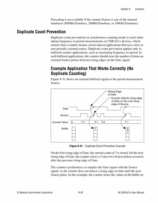
Chapter 8 Counters
© National Instruments Corporation 8-35 NI USB-621x User Manual
Prescaling is not available if the counter Source is one of the internal timebases (80MHzTimebase, 20MHzTimebase, or 100kHzTimebase).
Duplicate Count PreventionDuplicate count prevention (or synchronous counting mode) is used when taking frequency or period measurements on USB-621x devices, which ensures that a counter returns correct data in applications that use a slow or non-periodic external source. Duplicate count prevention applies only to buffered counter applications, such as measuring frequency or period. In such buffered applications, the counter should store the number of times an external Source pulses between rising edges on the Gate signal.
Example Application That Works Correctly (No Duplicate Counting)Figure 8-31 shows an external buffered signal as the period measurement Source.
Figure 8-31. Duplicate Count Prevention Example
On the first rising edge of Gate, the current count of 7 is stored. On the next rising edge of Gate, the counter stores a 2 since two Source pulses occurred after the previous rising edge of Gate.
The counter synchronizes or samples the Gate signal with the Source signal, so the counter does not detect a rising edge in Gate until the next Source pulse. In this example, the counter stores the values in the buffer on
Gate
2 7
7
6 7 1 2 1
Rising Edge of Gate
Counter detects rising edge of Gate on the next rising edge of Source.
Source
Counter Value
Buffer
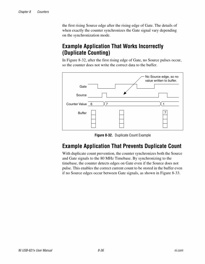
Chapter 8 Counters
NI USB-621x User Manual 8-36 ni.com
the first rising Source edge after the rising edge of Gate. The details of when exactly the counter synchronizes the Gate signal vary depending on the synchronization mode.
Example Application That Works Incorrectly (Duplicate Counting)In Figure 8-32, after the first rising edge of Gate, no Source pulses occur, so the counter does not write the correct data to the buffer.
Figure 8-32. Duplicate Count Example
Example Application That Prevents Duplicate CountWith duplicate count prevention, the counter synchronizes both the Source and Gate signals to the 80 MHz Timebase. By synchronizing to the timebase, the counter detects edges on Gate even if the Source does not pulse. This enables the correct current count to be stored in the buffer even if no Source edges occur between Gate signals, as shown in Figure 8-33.
Gate
Source
Counter Value
Buffer 7
6 7 1
No Source edge, so novalue written to buffer.
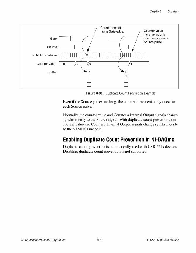
Chapter 8 Counters
© National Instruments Corporation 8-37 NI USB-621x User Manual
Figure 8-33. Duplicate Count Prevention Example
Even if the Source pulses are long, the counter increments only once for each Source pulse.
Normally, the counter value and Counter n Internal Output signals change synchronously to the Source signal. With duplicate count prevention, the counter value and Counter n Internal Output signals change synchronously to the 80 MHz Timebase.
Enabling Duplicate Count Prevention in NI-DAQmxDuplicate count prevention is automatically used with USB-621x devices. Disabling duplicate count prevention is not supported.
Gate
0 7
7
6 7 0 1
Counter detects rising Gate edge.
Source
Counter Value
Buffer
Counter value increments only one time for each Source pulse.
80 MHz Timebase

© National Instruments Corporation 9-1 NI USB-621x User Manual
9Isolation and Digital Isolators on USB-6215/6216/6218 Devices
USB-6215/6216/6218 devices are isolated data acquisition devices. The analog input, analog output, counters, PFI/static DI, and PFI/static DO circuitry1, and digital routing and clock generation are referenced to an isolated ground, as shown in Figure 9-1.
Figure 9-1. USB-6215/6216/6218 Block Diagram
The bus interface circuitry is referenced to a non-isolated ground. The following table lists the ground symbols.
1 USB-6216 devices have PFI/static DIO circuitry.
Ground Type Symbol
Isolated Ground
Non-Isolated Ground
Analog Output
Digital I/O
Analog Input
Counters
PFI
DigitalRouting
and ClockGeneration
BusInterface Bus
I/O C
onne
ctor
DigitalIsolators
IsolationBarrier
Chapter 9 Isolation and Digital Isolators on USB-6215/6216/6218 Devices
© National Instruments Corporation 9-2 NI USB-621x User Manual
The non-isolated ground is connected to the chassis ground of the PC.
Each isolated ground is not connected to the chassis ground of the PC. The isolated ground can be at a higher or lower voltage relative to the non-isolated ground. All analog measurements are made relative to the isolated ground signal.
The isolated ground is an input to the USB-6215/6216/6218 device. The user must connect this ground to the ground of system being measured or controlled. For more information, refer to the following:
• The Connecting Analog Input Signals on USB-6215/6216/6218 Devices section of Chapter 4, Analog Input
• The Connecting Analog Output Signals section of Chapter 5, Analog Output
• The Connecting Digital I/O Signals on USB-6210/6211/6215/6218 Devices or Connecting Digital I/O Signals on USB-6212/6216 Devices section of Chapter 6, Digital I/O
• The Connecting PFI Input Signals section of Chapter 7, PFI
Digital IsolationUSB-6215/6216/6218 devices use digital isolators. Unlike analog isolators, digital isolators do not introduce any analog error in the measurements taken by the device. The A/D converter, used for analog input, is on the isolated side of the device. The analog inputs are digitized before they are sent across the isolation barrier. Similarly, the D/A converters, used for analog output, are on the isolated side of the device.
Benefits of an Isolated DAQ DeviceWith isolation, engineers can safely measure a small signal in the presence of a large common-mode voltage signal. Some advantages of isolation are as follows:
• Improved rejection—Isolation increases the ability of the measurement system to reject common-mode voltages. Common-mode voltage is the signal that is present or “common” to both the positive and negative input of a measurement device, but is not part of the signal to be measured.
• Improved accuracy—Isolation improves measurement accuracy by physically preventing ground loops. Ground loops, a common source
Chapter 9 Isolation and Digital Isolators on USB-6215/6216/6218 Devices
NI USB-621x User Manual 9-3 ni.com
of error and noise, are the result of a measurement system having multiple grounds at different potentials.
• Improved safety—The isolation barrier allows you to make floating measurements while protecting the USB host computer against large transient voltage spikes.
Reducing Common-Mode NoiseIsolated products require an isolated power supply to deliver power to the isolated side from the non-isolated side. Isolated power supplies work by switching voltages through a transformer with high-speed transistors. Switching voltages through the transformer cause charging and discharging of the parasitic capacitances and inductances in the switching power supplies that occur on every switch cycle, resulting in high-speed currents flowing through the isolated side and returning to the non-isolated side, which is earth ground.
These parasitic currents interact with parasitic and non-parasitic resistances causing voltage spikes. These voltage spikes are called common-mode noise, a noise source that travels in the ground and is therefore common to both the ground and any signal referenced to the ground, such as AI, AO, and digital signals. Common-mode noise appears at the harmonics of the switching power supply frequency and can corrupt measurements depending on the system setup.
You can perform some tasks to reduce common-mode noise:
• Better grounding from the front connector AI GND to the signal source ground can reduce common-mode noise. Use low resistance cabling and connections and verify that all ground connections are kept short. Keep the number of connections to a minimum. If the device’s isolated ground is being connected back to earth ground, verify that this is done in the most direct way possible.
• Reduce source impedances if possible. The parasitic currents react with these impedances.
Creating an AC Return Path
Caution Adding a capacitor will degrade the USB-6215/6216/6218 device withstand voltage and isolation specifications. Withstand voltage must be retested by an approved testing facility after adjustments are made to the measurement system.
Chapter 9 Isolation and Digital Isolators on USB-6215/6216/6218 Devices
© National Instruments Corporation 9-4 NI USB-621x User Manual
Isolated SystemsA fully isolated measurement system is one where the device’s isolated front end is not connected back to earth ground.
Create an AC path back to earth ground from the device’s isolated ground by connecting a high voltage capacitor between the isolated board ground and earth ground. The voltage rating of the capacitor must be larger than the voltage drop between the isolated ground and earth ground.
Non-Isolated SystemsA non-isolated measurement system is one where the device’s isolated front end connects to earth ground.
Add an AC return path from the device isolated ground to earth ground. For non-isolated systems, an AC return path is only needed for high or source impedances. An AC return path can be created by connecting a capacitor between the device’s isolated ground and earth ground.
© National Instruments Corporation 10-1 NI USB-621x User Manual
10Digital Routing and Clock Generation
The digital routing circuitry has the following main functions:
• Manages the flow of data between the bus interface and the acquisition/generation sub-systems (analog input, analog output, digital I/O, and the counters). The digital routing circuitry uses FIFOs (if present) in each sub-system to ensure efficient data movement.
• Routes timing and control signals. The acquisition/generation sub-systems use these signals to manage acquisitions and generations. These signals can come from the following sources:
– Your USB-621x device
– User input through the PFI terminals
• Routes and generates the main clock signals for the USB-621x device.
80 MHz TimebaseThe 80 MHz Timebase can be used as the Source input to the 32-bit general-purpose counter/timers. The 80 MHz Timebase is generated from the onboard oscillator.
20 MHz TimebaseThe 20 MHz Timebase normally generates many of the AI and AO timing signals. The 20 MHz Timebase also can be used as the Source input to the 32-bit general-purpose counter/timers. The 20 MHz Timebase is generated by dividing down the 80 MHz Timebase.
100 kHz TimebaseThe 100 kHz Timebase can be used to generate many of the AI and AO timing signals. The 100 kHz Timebase also can be used as the Source input to the 32-bit general-purpose counter/timers. The 100 kHz Timebase is generated by dividing down the 20 MHz Timebase by 200.
© National Instruments Corporation 11-1 NI USB-621x User Manual
11Bus Interface
The bus interface circuitry of USB-621x devices efficiently moves data between host memory and the measurement and acquisition circuits.
All USB-621x devices are jumperless for complete plug-and-play operation. The operating system automatically assigns the base address, interrupt levels, and other resources.
USB-621x devices incorporate USB-STC2 technology to implement a Hi-Speed USB interface.
USB Signal StreamUSB-621x devices have four fully-independent USB Signal Streams for high-performance transfers of data blocks. One USB Signal Stream is available for each measurement and acquisition block:
• Analog input
• Analog output
• Counter 0
• Counter 1
Data Transfer MethodsThe two primary ways to transfer data across the USB bus are USB Signal Stream and programmed I/O:
• USB Signal Stream—A method to transfer data between the device and computer memory using USB bulk transfers without intervention of the microcontroller on the NI device. NI uses USB Signal Stream hardware and software technology to achieve high throughput rates and increase system utilization in USB devices.
• Programmed I/O—A data transfer mechanism where the user’s program is responsible for transferring data. Each read or write call in the program initiates the transfer of data. Programmed I/O is typically used in software-timed (on-demand) operations. Refer to the Analog
Chapter 11 Bus Interface
NI USB-621x User Manual 11-2 ni.com
Output Data Generation Methods section of Chapter 5, Analog Output, for more information.
Changing Data Transfer MethodsUSB-621x devices have four dedicated USB Signal Stream channels. To change your data transfer mechanism between USB Signal Streams and programmed I/O, use the Data Transfer Mechanism property node function in NI-DAQmx.
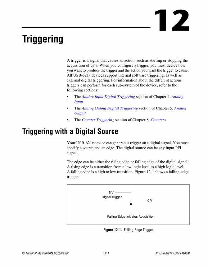
© National Instruments Corporation 12-1 NI USB-621x User Manual
12Triggering
A trigger is a signal that causes an action, such as starting or stopping the acquisition of data. When you configure a trigger, you must decide how you want to produce the trigger and the action you want the trigger to cause. All USB-621x devices support internal software triggering, as well as external digital triggering. For information about the different actions triggers can perform for each sub-system of the device, refer to the following sections:
• The Analog Input Digital Triggering section of Chapter 4, Analog Input
• The Analog Output Digital Triggering section of Chapter 5, Analog Output
• The Counter Triggering section of Chapter 8, Counters
Triggering with a Digital SourceYour USB-621x device can generate a trigger on a digital signal. You must specify a source and an edge. The digital source can be any input PFI signal.
The edge can be either the rising edge or falling edge of the digital signal. A rising edge is a transition from a low logic level to a high logic level. A falling edge is a high to low transition. Figure 12-1 shows a falling-edge trigger.
Figure 12-1. Falling-Edge Trigger
5 V
0 V
Falling Edge Initiates Acquisition
Digital Trigger
Chapter 12 Triggering
NI USB-621x User Manual 12-2 ni.com
You also can program your USB-621x device to perform an action in response to a trigger from a digital source. The action can affect the following:
• Analog input acquisition
• Analog output generation
• Counter behavior
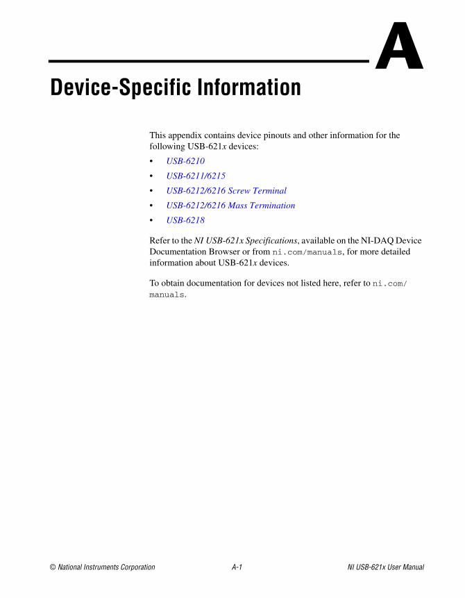
© National Instruments Corporation A-1 NI USB-621x User Manual
ADevice-Specific Information
This appendix contains device pinouts and other information for the following USB-621x devices:
• USB-6210
• USB-6211/6215
• USB-6212/6216 Screw Terminal
• USB-6212/6216 Mass Termination
• USB-6218
Refer to the NI USB-621x Specifications, available on the NI-DAQ Device Documentation Browser or from ni.com/manuals, for more detailed information about USB-621x devices.
To obtain documentation for devices not listed here, refer to ni.com/manuals.
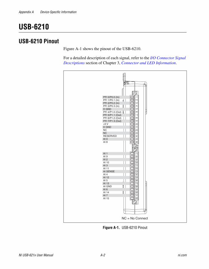
Appendix A Device-Specific Information
NI USB-621x User Manual A-2 ni.com
USB-6210
USB-6210 PinoutFigure A-1 shows the pinout of the USB-6210.
For a detailed description of each signal, refer to the I/O Connector Signal Descriptions section of Chapter 3, Connector and LED Information.
Figure A-1. USB-6210 Pinout
56
78
12
34
1314
1516
910
1112
AI 1AI 9AI 2AI 10AI 3AI 11AI SENSEAI 4AI 12AI 5AI 13AI GNDAI 6AI 14AI 7AI 15
PFI 0/P0.0 (In)PFI 1/P0.1 (In)PFI 2/P0.2 (In)PFI 3/P0.3 (In)D GNDPFI 4/P1.0 (Out)PFI 5/P1.1 (Out)PFI 6/P1.2 (Out)PFI 7/P1.3 (Out)+5 VD GNDNCNCRESERVEDAI 0AI 8
2122
2324
1718
1920
2930
3132
2526
2728
NC = No Connect

Appendix A Device-Specific Information
© National Instruments Corporation A-3 NI USB-621x User Manual
Note For more information about default NI-DAQmx counter inputs, refer to Connecting Counter Signals in the NI-DAQmx Help or the LabVIEW Help in version 8.0 or later.
Table A-1. Default NI-DAQmx Counter/Timer Pins
Counter/Timer Signal Default Terminal Number (Name)
CTR 0 SRC 1 (PFI 0)
CTR 0 GATE 2 (PFI 1)
CTR 0 AUX 1 (PFI 0)
CTR 0 OUT 6 (PFI 4)
CTR 0 A 1 (PFI 0)
CTR 0 Z 3 (PFI 2)
CTR 0 B 2 (PFI 1)
CTR 1 SRC 4 (PFI 3)
CTR 1 GATE 3 (PFI 2)
CTR 1 AUX 4 (PFI 3)
CTR 1 OUT 7 (PFI 5)
CTR 1 A 4 (PFI 3)
CTR 1 Z 2 (PFI 1)
CTR 1 B 3 (PFI 2)
FREQ OUT 8 (PFI 6)
Appendix A Device-Specific Information
NI USB-621x User Manual A-4 ni.com
USB-6211/6215
USB-6211/6215 PinoutFigure A-2 shows the pinout of the USB-6211 and USB-6215.
For a detailed description of each signal, refer to the I/O Connector Signal Descriptions section of Chapter 3, Connector and LED Information.
Figure A-2. USB-6211/6215 Pinout
56
78
12
34
1314
1516
910
1112
AI 1AI 9AI 2AI 10AI 3AI 11AI SENSEAI 4AI 12AI 5AI 13AI GNDAI 6AI 14AI 7AI 15
PFI 0/P0.0 (In)PFI 1/P0.1 (In)PFI 2/P0.2 (In)PFI 3/P0.3 (In)D GNDPFI 4/P1.0 (Out)PFI 5/P1.1 (Out)PFI 6/P1.2 (Out)PFI 7/P1.3 (Out)+5 VD GNDAO 0AO 1AO GNDAI 0AI 8
2122
2324
1718
1920
2930
3132
2526
2728
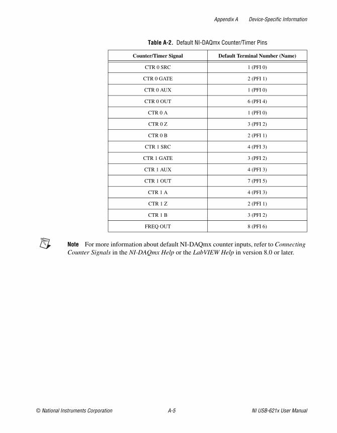
Appendix A Device-Specific Information
© National Instruments Corporation A-5 NI USB-621x User Manual
Note For more information about default NI-DAQmx counter inputs, refer to Connecting Counter Signals in the NI-DAQmx Help or the LabVIEW Help in version 8.0 or later.
Table A-2. Default NI-DAQmx Counter/Timer Pins
Counter/Timer Signal Default Terminal Number (Name)
CTR 0 SRC 1 (PFI 0)
CTR 0 GATE 2 (PFI 1)
CTR 0 AUX 1 (PFI 0)
CTR 0 OUT 6 (PFI 4)
CTR 0 A 1 (PFI 0)
CTR 0 Z 3 (PFI 2)
CTR 0 B 2 (PFI 1)
CTR 1 SRC 4 (PFI 3)
CTR 1 GATE 3 (PFI 2)
CTR 1 AUX 4 (PFI 3)
CTR 1 OUT 7 (PFI 5)
CTR 1 A 4 (PFI 3)
CTR 1 Z 2 (PFI 1)
CTR 1 B 3 (PFI 2)
FREQ OUT 8 (PFI 6)
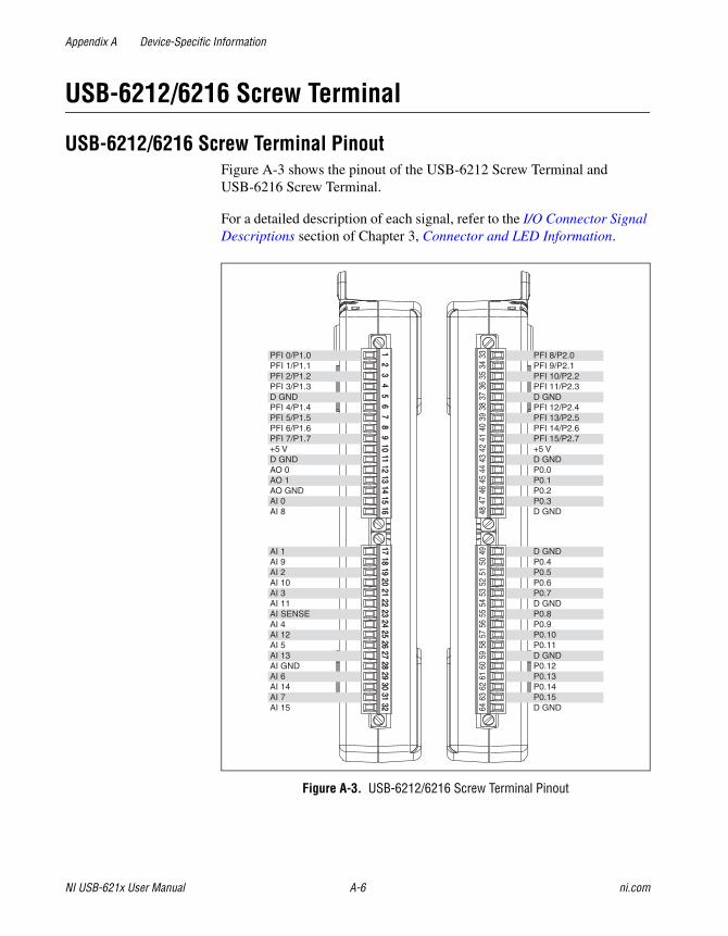
Appendix A Device-Specific Information
NI USB-621x User Manual A-6 ni.com
USB-6212/6216 Screw Terminal
USB-6212/6216 Screw Terminal PinoutFigure A-3 shows the pinout of the USB-6212 Screw Terminal and USB-6216 Screw Terminal.
For a detailed description of each signal, refer to the I/O Connector Signal Descriptions section of Chapter 3, Connector and LED Information.
Figure A-3. USB-6212/6216 Screw Terminal Pinout
AI 1AI 9AI 2AI 10AI 3AI 11AI SENSEAI 4AI 12AI 5AI 13AI GNDAI 6AI 14AI 7AI 15
PFI 0/P1.0PFI 1/P1.1PFI 2/P1.2PFI 3/P1.3D GNDPFI 4/P1.4PFI 5/P1.5PFI 6/P1.6PFI 7/P1.7+5 VD GNDAO 0AO 1AO GNDAI 0AI 8
56
78
12
34
1314
1516
910
1112
2122
2324
1718
1920
2930
3132
2526
2728
D GNDP0.4P0.5P0.6P0.7D GNDP0.8P0.9P0.10P0.11D GNDP0.12P0.13P0.14P0.15D GND
PFI 8/P2.0PFI 9/P2.1PFI 10/P2.2PFI 11/P2.3D GNDPFI 12/P2.4PFI 13/P2.5PFI 14/P2.6PFI 15/P2.7+5 VD GNDP0.0P0.1P0.2P0.3D GND
56
78
12
34
1314
1516
910
1112
2122
2324
1718
1920
2930
3132
2526
2728 60
5958
5764
6362
6152
5150
4956
5554
5344
4342
4148
4746
4536
3534
3340
3938
37

Appendix A Device-Specific Information
© National Instruments Corporation A-7 NI USB-621x User Manual
Note For more information about default NI-DAQmx counter inputs, refer to Connecting Counter Signals in the NI-DAQmx Help or the LabVIEW Help in version 8.0 or later.
Table A-3. Default NI-DAQmx Counter/Timer Pins
Counter/Timer Signal Default Terminal Number (Name)
CTR 0 SRC 33 (PFI 8)
CTR 0 GATE 34 (PFI 9)
CTR 0 AUX 35 (PFI 10)
CTR 0 OUT 38 (PFI 12)
CTR 0 A 33 (PFI 8)
CTR 0 Z 34 (PFI 9)
CTR 0 B 35 (PFI 10)
CTR 1 SRC 4 (PFI 3)
CTR 1 GATE 6 (PFI 4)
CTR 1 AUX 36 (PFI 11)
CTR 1 OUT 39 (PFI 13)
CTR 1 A 4 (PFI 3)
CTR 1 Z 6 (PFI 4)
CTR 1 B 36 (PFI 11)
FREQ OUT 40 (PFI 14)
Appendix A Device-Specific Information
NI USB-621x User Manual A-8 ni.com
USB-6212/6216 Mass Termination
USB-6212/6216 Mass Termination PinoutFigure A-4 shows the pinout of the USB-6212 Mass Termination and USB-6216 Mass Termination.
For a detailed description of each signal, refer to the I/O Connector Signal Descriptions section of Chapter 3, Connector and LED Information.
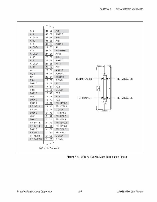
Appendix A Device-Specific Information
© National Instruments Corporation A-9 NI USB-621x User Manual
Figure A-4. USB-6212/6216 Mass Termination Pinout
PFI 14/P2.6
PFI 12/P2.4
PFI 9/P2.1
D GND
PFI 6/P1.6
PFI 5/P1.5
D GND
+5 V
D GND
PFI 1/P1.1
PFI 0/P1.0
D GND
D GND
+5 V
D GND
P0.6
P0.1
D GND
P0.4NC
AO 1
AO 0
AI 15
AI GND
AI 6
AI 13
AI GND
AI 4
AI GND
AI 3
AI 10
AI GND
AI 1
AI 8
D GND
PFI 8/P2.0
PFI 7/P1.7
PFI 13/P2.5
PFI 4/P1.4
PFI 3/P1.3
PFI 2/P1.2
D GND
PFI 15/P2.7
D GND
PFI 10/P2.2
PFI 11/P2.3
P0.3
P0.7
P0.2
D GND
P0.5
P0.0
D GNDAO GND
AO GND
AI GND
AI 7
AI 14
AI GND
AI 5
AI 12
AI SENSE
AI 11
AI GND
AI 2
AI 9
AI GND
AI 0
1
2
3
4
5
6
7
8
9
10
11
12
13
14
15
16
17
18
19
20
21
22
23
24
25
26
27
28
29
30
31
32
33
34
35
36
37
38
39
40
41
42
43
44
45
46
47
48
49
50
51
52
53
54
55
56
57
58
59
60
61
62
63
64
65
66
67
68
TERMINAL 1
TERMINAL 34
TERMINAL 35
TERMINAL 68
NC = No Connect
Appendix A Device-Specific Information
NI USB-621x User Manual A-10 ni.com
Note For more information about default NI-DAQmx counter inputs, refer to Connecting Counter Signals in the NI-DAQmx Help or the LabVIEW Help in version 8.0 or later.
USB-6212/6216 Mass Termination Cables and AccessoriesThis section describes some cable and accessory options for USB-6212/6216 Mass Termination devices. Refer to ni.com for other accessory options including new devices.
SCC AccessoriesSCC provides portable, modular signal conditioning to your DAQ system. To connect your USB-6212/6216 Mass Termination device to an SCC module carrier, such as the SC-2345, SC-2350, or SCC-68, use an SH68-68-EPM shielded cable. The SCC carrier must be externally powered when used with a USB-6212/6216 Mass Termination device. Refer to the +5 V Power section of Chapter 3, Connector and LED Information, and the NI USB-621x Specifications for more information.
Table A-4. Default NI-DAQmx Counter/Timer Pins
Counter/Timer Signal Default Terminal Number (Name)
CTR 0 SRC 37 (PFI 8)
CTR 0 GATE 3 (PFI 9)
CTR 0 AUX 45 (PFI 10)
CTR 0 OUT 2 (PFI 12)
CTR 0 A 37 (PFI 8)
CTR 0 Z 3 (PFI 9)
CTR 0 B 45 (PFI 10)
CTR 1 SRC 42 (PFI 3)
CTR 1 GATE 41 (PFI 4)
CTR 1 AUX 46 (PFI 11)
CTR 1 OUT 40 (PFI 13)
CTR 1 A 42 (PFI 3)
CTR 1 Z 41 (PFI 4)
CTR 1 B 46 (PFI 11)
FREQ OUT 1 (PFI 14)
Appendix A Device-Specific Information
© National Instruments Corporation A-11 NI USB-621x User Manual
Refer to the SCC Advisor, available by going to ni.com/info and entering the info code rdscav, for more information.
BNC AccessoriesYou can use the SH68-68-EPM shielded cable, to connect the USB-6212/6216 Mass Termination device to BNC accessories, such as the following:
• BNC-2110—Provides BNC connectivity to all analog signals, some digital signals, and spring terminals for other digital signals
• BNC-2111—Provides BNC connectivity to 16 single-ended analog input signals, two analog output signals, five DIO/PFI signals, and the external reference voltage for analog output
• BNC-2120—Similar to the BNC-2110, and also has a built-in function generator, quadrature encoder, temperature reference, and thermocouple connector
• BNC-2090A—Desktop/rack-mountable device with 22 BNCs for connecting analog, digital, and timing signals
Screw Terminal AccessoriesNational Instruments offers several styles of screw terminal connector blocks. Use an SH68-68-EPM shielded cable to connect a USB-6212/6216 Mass Termination device to a connector block, such as the following:
• CB-68LP and CB-68LPR unshielded connector blocks
• SCC-68 I/O connector block with screw terminals, general breadboard area, bus terminals, and four expansion slots for SCC signal conditioning modules
• SCB-68 shielded connector block with temperature sensor
• TBX-68 DIN rail-mountable connector block
CablesIn most applications, you can use the following cables:
• SH68-68-EPM—High-performance cable with individual bundles separating analog and digital signals. Each differential analog input channel is routed on an individually shielded twisted pair of wires. Analog outputs are also individually shielded
• R68-68—Highly-flexible unshielded ribbon cable
Appendix A Device-Specific Information
NI USB-621x User Manual A-12 ni.com
Custom Cabling and ConnectivityThe CA-1000 is a configurable enclosure that gives user-defined connectivity and flexibility through customized panelettes. Visit ni.com for more information about the CA-1000.
Refer to the USB-621x Mass Termination Custom Cabling section of Chapter 2, DAQ System Overview, for more information about custom cabling solutions.
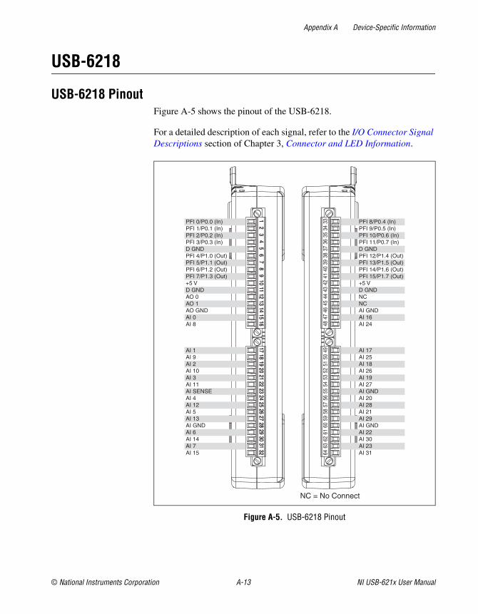
Appendix A Device-Specific Information
© National Instruments Corporation A-13 NI USB-621x User Manual
USB-6218
USB-6218 PinoutFigure A-5 shows the pinout of the USB-6218.
For a detailed description of each signal, refer to the I/O Connector Signal Descriptions section of Chapter 3, Connector and LED Information.
Figure A-5. USB-6218 Pinout
AI 1AI 9AI 2AI 10AI 3AI 11AI SENSEAI 4AI 12AI 5AI 13AI GNDAI 6AI 14AI 7AI 15
PFI 0/P0.0 (In)PFI 1/P0.1 (In)PFI 2/P0.2 (In)PFI 3/P0.3 (In)D GNDPFI 4/P1.0 (Out)PFI 5/P1.1 (Out)PFI 6/P1.2 (Out)PFI 7/P1.3 (Out)+5 VD GNDAO 0AO 1AO GNDAI 0AI 8
56
78
12
34
1314
1516
910
1112
2122
2324
1718
1920
2930
3132
2526
2728
AI 17AI 25AI 18AI 26AI 19AI 27AI GNDAI 20AI 28AI 21AI 29AI GNDAI 22AI 30AI 23AI 31
PFI 8/P0.4 (In)PFI 9/P0.5 (In)PFI 10/P0.6 (In)PFI 11/P0.7 (In)D GNDPFI 12/P1.4 (Out)PFI 13/P1.5 (Out)PFI 14/P1.6 (Out)PFI 15/P1.7 (Out)+5 VD GNDNCNCAI GNDAI 16AI 24
56
78
12
34
1314
1516
910
1112
2122
2324
1718
1920
2930
3132
2526
2728 60
5958
5764
6362
6152
5150
4956
5554
5344
4342
4148
4746
4536
3534
3340
3938
37
NC = No Connect
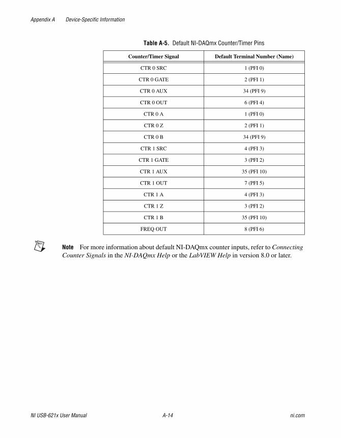
Appendix A Device-Specific Information
NI USB-621x User Manual A-14 ni.com
Note For more information about default NI-DAQmx counter inputs, refer to Connecting Counter Signals in the NI-DAQmx Help or the LabVIEW Help in version 8.0 or later.
Table A-5. Default NI-DAQmx Counter/Timer Pins
Counter/Timer Signal Default Terminal Number (Name)
CTR 0 SRC 1 (PFI 0)
CTR 0 GATE 2 (PFI 1)
CTR 0 AUX 34 (PFI 9)
CTR 0 OUT 6 (PFI 4)
CTR 0 A 1 (PFI 0)
CTR 0 Z 2 (PFI 1)
CTR 0 B 34 (PFI 9)
CTR 1 SRC 4 (PFI 3)
CTR 1 GATE 3 (PFI 2)
CTR 1 AUX 35 (PFI 10)
CTR 1 OUT 7 (PFI 5)
CTR 1 A 4 (PFI 3)
CTR 1 Z 3 (PFI 2)
CTR 1 B 35 (PFI 10)
FREQ OUT 8 (PFI 6)
© National Instruments Corporation B-1 NI USB-621x User Manual
BTroubleshooting
This section contains common questions about USB-621x devices. If your questions are not answered here, refer to the National Instruments KnowledgeBase at ni.com/kb.
Analog InputI am seeing crosstalk or ghost voltages when sampling multiple channels. What does this mean?
You may be experiencing a phenomenon called charge injection, which occurs when you sample a series of high-output impedance sources with a multiplexer. Multiplexers contain switches, usually made of switched capacitors. When a channel, for example AI 0, is selected in a multiplexer, those capacitors accumulate charge. When the next channel, for example AI 1, is selected, the accumulated current (or charge) leaks backward through channel 1. If the output impedance of the source connected to AI 1 is high enough, the resulting reading can somewhat affect the voltage in AI 0. To circumvent this problem, use a voltage follower that has operational amplifiers (op-amps) with unity gain for each high-impedance source before connecting to a USB-621x device. Otherwise, you must decrease the sample rate for each channel.
Another common cause of channel crosstalk is due to sampling among multiple channels at various gains. In this situation, the settling times can increase. For more information about charge injection and sampling channels at different gains, refer to the Multichannel Scanning Considerations section of Chapter 4, Analog Input.
I am using my device in differential analog input ground-reference mode and I have connected a differential input signal, but my readings are random and drift rapidly. What is wrong?
In DIFF mode, if the readings from the DAQ device are random and drift rapidly, you should check the ground-reference connections. The signal can be referenced to a level that is considered floating with reference to the device ground reference. Even if you are in DIFF mode, you must still reference the signal to the same ground level as the device reference. There
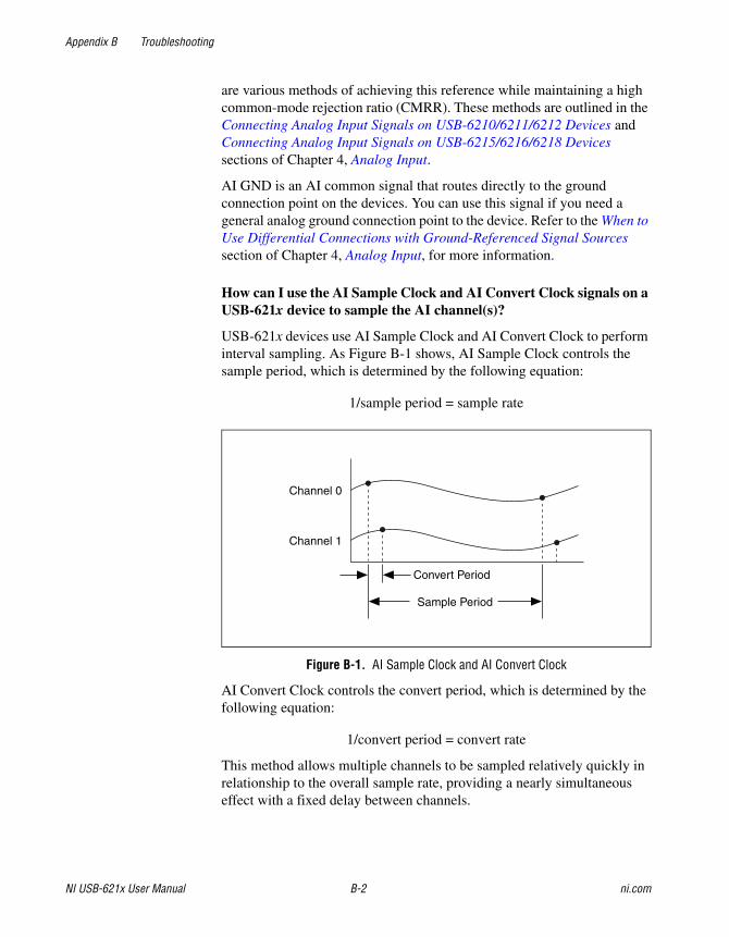
Appendix B Troubleshooting
NI USB-621x User Manual B-2 ni.com
are various methods of achieving this reference while maintaining a high common-mode rejection ratio (CMRR). These methods are outlined in the Connecting Analog Input Signals on USB-6210/6211/6212 Devices and Connecting Analog Input Signals on USB-6215/6216/6218 Devices sections of Chapter 4, Analog Input.
AI GND is an AI common signal that routes directly to the ground connection point on the devices. You can use this signal if you need a general analog ground connection point to the device. Refer to the When to Use Differential Connections with Ground-Referenced Signal Sources section of Chapter 4, Analog Input, for more information.
How can I use the AI Sample Clock and AI Convert Clock signals on a USB-621x device to sample the AI channel(s)?
USB-621x devices use AI Sample Clock and AI Convert Clock to perform interval sampling. As Figure B-1 shows, AI Sample Clock controls the sample period, which is determined by the following equation:
1/sample period = sample rate
Figure B-1. AI Sample Clock and AI Convert Clock
AI Convert Clock controls the convert period, which is determined by the following equation:
1/convert period = convert rate
This method allows multiple channels to be sampled relatively quickly in relationship to the overall sample rate, providing a nearly simultaneous effect with a fixed delay between channels.
Channel 0
Channel 1
Convert Period
Sample Period
Appendix B Troubleshooting
© National Instruments Corporation B-3 NI USB-621x User Manual
Analog OutputI am seeing glitches on the output signal. How can I minimize it?
When you use a DAC to generate a waveform, you may observe glitches on the output signal. These glitches are normal; when a DAC switches from one voltage to another, it produces glitches due to released charges. The largest glitches occur when the most significant bit of the DAC code changes. You can build a lowpass deglitching filter to remove some of these glitches, depending on the frequency and nature of the output signal. Visit ni.com/support for more information about minimizing glitches.
© National Instruments Corporation C-1 NI USB-621x User Manual
CTechnical Support and Professional Services
Visit the following sections of the National Instruments Web site at ni.com for technical support and professional services:
• Support—Technical support resources at ni.com/support include the following:
– Self-Help Technical Resources—For answers and solutions, visit the award-winning National Instruments Web site for software drivers and updates, a searchable KnowledgeBase, product manuals, step-by-step troubleshooting wizards, thousands of example programs, tutorials, application notes, instrument drivers, and so on. Registered users also receive access to the NI Discussion Forums at ni.com/forums. NI Applications Engineers make sure every question submitted online receives an answer.
– Standard Service Program Membership—This program entitles members to direct access to NI Applications Engineers via phone and email for one-to-one technical support as well as exclusive access to ondemand training modules via the Services Resource Center. NI offers complementary membership for a full year after purchase, after which you may renew to continue your benefits.
For information about other technical support options in your area, visit ni.com/services, or contact your local office at ni.com/contact.
• Training and Certification—Visit ni.com/training for self-paced training, eLearning virtual classrooms, interactive CDs, and Certification program information. You also can register for instructor-led, hands-on courses at locations around the world.
• System Integration—If you have time constraints, limited in-house technical resources, or other project challenges, National Instruments Alliance Partner members can help. To learn more, call your local NI office or visit ni.com/alliance.
Appendix C Technical Support and Professional Services
NI USB-621x User Manual C-2 ni.com
• Declaration of Conformity (DoC)—A DoC is our claim of compliance with the Council of the European Communities using the manufacturer’s declaration of conformity. This system affords the user protection for electronic compatibility (EMC) and product safety. You can obtain the DoC for your product by visiting ni.com/certification.
• Calibration Certificate—If your product supports calibration, you can obtain the calibration certificate for your product at ni.com/calibration.
If you searched ni.com and could not find the answers you need, contact your local office or NI corporate headquarters. Phone numbers for our worldwide offices are listed at the front of this manual. You also can visit the Worldwide Offices section of ni.com/niglobal to access the branch office Web sites, which provide up-to-date contact information, support phone numbers, email addresses, and current events.
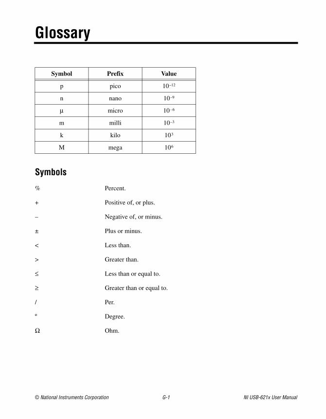
© National Instruments Corporation G-1 NI USB-621x User Manual
Glossary
Symbol Prefix Value
p pico 10–12
n nano 10–9
μ micro 10–6
m milli 10–3
k kilo 103
M mega 106
Symbols
% Percent.
+ Positive of, or plus.
– Negative of, or minus.
± Plus or minus.
< Less than.
> Greater than.
≤ Less than or equal to.
≥ Greater than or equal to.
/ Per.
º Degree.
Ω Ohm.
Glossary
NI USB-621x User Manual G-2 ni.com
A
A Amperes—the unit of electric current.
A/D Analog-to-Digital. Most often used as A/D converter.
AC Alternating current.
accuracy A measure of the capability of an instrument or sensor to faithfully indicate the value of the measured signal. This term is not related to resolution; however, the accuracy level can never be better than the resolution of the instrument.
ADE Application development environment.
AI 1. Analog input.
2. Analog input channel signal.
AI GND Analog input ground signal.
AI SENSE Analog input sense signal.
analog A signal whose amplitude can have a continuous range of values.
analog input signal An input signal that varies smoothly over a continuous range of values, rather than in discrete steps.
analog output signal An output signal that varies smoothly over a continuous range of values, rather than in discrete steps.
analog trigger A trigger that occurs at a user-selected point on an incoming analog signal. Triggering can be set to occur at a specific level on either an increasing or a decreasing signal (positive or negative slope). Analog triggering can be implemented either in software or in hardware. When implemented in software (LabVIEW), all data is collected, transferred into system memory, and analyzed for the trigger condition. When analog triggering is implemented in hardware, no data is transferred to system memory until the trigger condition has occurred.
AO Analog output.
AO GND Analog output ground signal.
application A software program that creates an end-user function.
Glossary
© National Instruments Corporation G-3 NI USB-621x User Manual
arm The process of getting an instrument ready to perform a function. For example, the trigger circuitry of a digitizer is armed, meaning that it is ready to start acquiring data when an appropriate trigger condition is met.
ASIC Application-specific integrated circuit—A proprietary semiconductor component designed and manufactured to perform a set of specific functions for a specific customer.
asynchronous 1. Hardware—A property of an event that occurs at an arbitrary time, without synchronization to a reference clock.
2. Software—A property of a function that begins an operation and returns prior to the completion or termination of the operation.
B
b Bit—One binary digit, either 0 or 1.
B Byte—Eight related bits of data, an eight-bit binary number. Also used to denote the amount of memory required to store one byte of data.
block diagram A pictorial description or representation of a program or algorithm.
buffer 1. Temporary storage for acquired or generated data.
2. A memory device that stores intermediate data between two devices.
bus, buses The group of electrical conductors that interconnect individual circuitry in a computer. Typically, a bus is the expansion vehicle to which I/O or other devices are connected. Examples of PC buses are the PCI, AT (ISA), and EISA bus.
C
C Celsius.
calibration The process of determining the accuracy of an instrument. In a formal sense, calibration establishes the relationship of an instrument’s measurement to the value provided by a standard. When that relationship is known, the instrument may then be adjusted (calibrated) for best accuracy.
cascading Process of extending the counting range of a counter chip by connecting to the next higher counter.
Glossary
NI USB-621x User Manual G-4 ni.com
CE European emissions control standard.
channel Pin or wire lead to which you apply or from which you read the analog or digital signal. Analog signals can be single-ended or differential. For digital signals, you group channels to form ports. Ports usually consist of either four or eight digital channels.
clock Hardware component that controls timing for reading from or writing to groups.
CMOS Complementary metal-oxide semiconductor.
CMRR Common-mode rejection ratio—A measure of the ability of a differential amplifier to reject interference from a common-mode signal, usually expressed in decibels (dB).
common-mode rejection
The ability of an electronic system to cancel any electronic noise pick-up that is common to both the positive and negative polarities of the input leads to the instrument front end. Common mode rejection is only a relevant specification for systems having a balanced or differential input.
common-mode signal 1. Any voltage present at the instrumentation amplifier inputs with respect to amplifier ground.
2. The signal, relative to the instrument chassis or computer’s ground, of the signals from a differential input. This is often a noise signal, such as 50 or 60 Hz hum.
connector 1. A device that provides electrical connection.
2. A fixture (either male or female) attached to a cable or chassis for quickly making and breaking one or more circuits. A symbol that connects points on a flowchart.
convert rate Reciprocal of the interchannel delay.
count The number of events, such as zero crossings, pulses, or cycles.
counter 1. Software. A memory location used to store a count of certain occurrences.
2. Hardware. A circuit that counts events. When it refers to an instrument, it refers to a frequency counter.
counter/timer A circuit that counts external pulses or clock pulses (timing).
Glossary
© National Instruments Corporation G-5 NI USB-621x User Manual
D
D GND Digital ground signal.
DAC Digital-to-Analog Converter—An electronic device, often an integrated circuit, that converts a digital number into a corresponding analog voltage or current.
In the instrumentation world, DACs can be used to generate arbitrary waveform shapes, defined by the software algorithm that computes the digital data pattern, which is fed to the DAC.
DAQ Data acquisition—The process of collecting and measuring electrical signals from sensors, transducers, and test probes or fixtures and inputting them to a computer for processing.
DAQ-STC2 Data acquisition system timing controller chip.
data acquisition The general concept of acquiring data, as in begin data acquisition or data acquisition and control. See also DAQ.
data transfer A technique for moving digital data from one system to another.
Options for data transfer are DMA, interrupt, and programmed I/O. For programmed I/O transfers, the CPU in the PC reads data from the DAQ device whenever the CPU receives a software signal to acquire a single data point. Interrupt-based data transfers occur when the DAQ device sends an interrupt to the CPU, telling the CPU to read the acquired data from the DAQ device. DMA transfers use a DMA controller, instead of the CPU, to move acquired data from the device into computer memory. Even though high-speed data transfers can occur with interrupt and programmed I/O transfers, they require the use of the CPU to transfer data. DMA transfers are able to acquire data at high speeds and keep the CPU free for performing other tasks at the same time.
dB Decibel—The unit for expressing a logarithmic measure of the ratio of two signal levels: dB = 20log10 V1/V2, for signals in volts.
DC Direct current—although the term speaks of current, many different types of DC measurements are made, including DC Voltage, DC current, and DC power.
device An electronic board that performs general analog or digital I/O functions on one or multiple channels, connected to a PC through a bus or I/O port, such as PCI, PXI, Ethernet, USB, or serial.
Glossary
NI USB-621x User Manual G-6 ni.com
DIFF Differential mode—An analog input mode consisting of two terminals, both of which are isolated from computer ground, whose difference is measured.
differential input An input circuit that actively responds to the difference between two terminals, rather than the difference between one terminal and ground. Often associated with balanced input circuitry, but also may be used with an unbalanced source.
digital I/O The capability of an instrument to generate and acquire digital signals.
Static digital I/O refers to signals where the values are set and held, or rarely change. Dynamic digital I/O refers to digital systems where the signals are continuously changing, often at multi-MHz clock rates.
digital signal A representation of information by a set of discrete values according to a prescribed law. These values are represented by numbers.
digital trigger A TTL level signal having two discrete levels—A high and a low level.
DIO Digital input/output.
DMA Direct Memory Access—A method by which data can be transferred to/from computer memory from/to a device or memory on the bus while the processor does something else. DMA is the fastest method of transferring data to/from computer memory.
DMA controller chip Performs the transfers between memory and I/O devices independently of the CPU.
driver Software unique to the device or type of device, and includes the set of commands the device accepts.
E
edge detection A technique that locates an edge of an analog signal, such as the edge of a square wave.
EEPROM Electrically Erasable Programmable Read-Only Memory—ROM that can be erased with an electrical signal and reprogrammed. Some SCXI modules contain an EEPROM to store measurement-correction coefficients.
Glossary
© National Instruments Corporation G-7 NI USB-621x User Manual
encoder A device that converts linear or rotary displacement into digital or pulse signals. The most popular type of encoder is the optical encoder, which uses a rotating disk with alternating opaque areas, a light source, and a photodetector.
external trigger A voltage pulse from an external source that causes a DAQ operation to begin.
F
FIFO First-In-First-Out memory buffer—A data buffering technique that functions like a shift register where the oldest values (first in) come out first. Many DAQ products and instruments use FIFOs to buffer digital data from an A/D converter, or to buffer the data before or after bus transmission.
The first data stored is the first data sent to the acceptor. FIFOs are often used on DAQ devices to temporarily store incoming or outgoing data until that data can be retrieved or output. For example, an analog input FIFO stores the results of A/D conversions until the data can be retrieved into system memory, a process that requires the servicing of interrupts and often the programming of the DMA controller. This process can take several milliseconds in some cases. During this time, data accumulates in the FIFO for future retrieval. With a larger FIFO, longer latencies can be tolerated. In the case of analog output, a FIFO permits faster update rates, because the waveform data can be stored on the FIFO ahead of time. This again reduces the effect of latencies associated with getting the data from system memory to the DAQ device.
filter A physical device or digital algorithm that selectively removes noise from a signal, or emphasizes certain frequency ranges and de-emphasizes others. Electronic filters include lowpass, band-pass, and highpass types. Digital filters can operate on numeric data to perform equivalent operations on digitized analog data or to enhance video images.
filtering A type of signal conditioning that allows you to filter unwanted frequency components from the signal you are trying to measure.
floating The condition where a common mode voltage exists, or may exist, between earth ground and the instrument or circuit of interest. Neither the high, nor the low side of a circuit is at earth potential.
Glossary
NI USB-621x User Manual G-8 ni.com
floating signal sources Signal sources with voltage signals that are not connected to an absolute reference of system ground. Also called non-referenced signal sources. Some common examples of floating signal sources are batteries, transformers, and thermocouples.
FREQ OUT Frequency Output signal.
frequency The number of alternating signals that occur per unit time.
ft Feet.
function 1. A built-in execution element, comparable to an operator, function, or statement in a conventional language.
2. A set of software instructions executed by a single line of code that may have input and/or output parameters and returns a value when executed.
G
glitch An unwanted signal excursion of short duration that is usually unavoidable.
GND See ground.
ground 1. A pin.
2. An electrically neutral wire that has the same potential as the surrounding earth. Normally, a noncurrent-carrying circuit intended for safety.
3. A common reference point for an electrical system.
H
hardware The physical components of a computer system, such as the circuit boards, plug-in devices, chassis, enclosures, peripherals, and cables.
hardware triggering A form of triggering where you set the start time of an acquisition and gather data at a known position in time relative to a trigger signal.
Hz 1. Hertz—The SI unit for measurement of frequency. One hertz (Hz) equals one cycle per second.
2. The number of scans read or updates written per second.
Glossary
© National Instruments Corporation G-9 NI USB-621x User Manual
I
I/O Input/Output—The transfer of data to/from a computer system involving communications channels, operator interface devices, and/or data acquisition and control interfaces.
impedance 1. The electrical characteristic of a circuit expressed in ohms and/or capacitance/inductance.
2. Resistance.
in. Inch or inches.
instrument driver A set of high-level software functions that controls a specific GPIB, VXI, or RS232 programmable instrument or a specific plug-in DAQ device. Instrument drivers are available in several forms, ranging from a function callable language to a virtual instrument (VI) in LabVIEW.
instrumentation amplifier
A circuit whose output voltage with respect to ground is proportional to the difference between the voltages at its two inputs. An instrumentation amplifier normally has high-impedance differential inputs and high common-mode rejection.
interchannel delay Amount of time that passes between sampling consecutive channels in an AI scan list. The interchannel delay must be short enough to allow sampling of all the channels in the channel list, within the sample interval. The greater the interchannel delay, the more time the PGIA is allowed to settle before the next channel is sampled. The interchannel delay is regulated by AI Convert Clock.
interface Connection between one or more of the following: hardware, software, and the user. For example, hardware interfaces connect two other pieces of hardware.
interrupt, interrupt request line
1. A means for a device to notify another device that an event occurred.
2. A computer signal indicating that the CPU should suspend its current task to service a designated activity.
IOH Current, output high.
IOL Current, output low.
IRQ See interrupt, interrupt request line.
Glossary
NI USB-621x User Manual G-10 ni.com
L
LabVIEW A graphical programming language.
LED Light-Emitting Diode—A semiconductor light source.
lowpass filter A filter that passes signals below a cutoff frequency while blocking signals above that frequency.
LSB Least Significant Bit.
M
m Meter.
M Series An architecture for instrumentation-class, multichannel data acquisition devices based on the earlier E Series architecture with added new features.
measurement The quantitative determination of a physical characteristic. In practice, measurement is the conversion of a physical quantity or observation to a domain where a human being or computer can determine the value.
MIO Multifunction I/O—DAQ module. Designates a family of data acquisition products that have multiple analog input channels, digital I/O channels, timing, and optionally, analog output channels. An MIO product can be considered a miniature mixed signal tester, due to its broad range of signal types and flexibility. Also known as multifunction DAQ.
module A board assembly and its associated mechanical parts, front panel, optional shields, and so on. A module contains everything required to occupy one or more slots in a mainframe. SCXI and PXI devices are modules.
monotonicity A characteristic of a DAC in which the analog output always increases as the values of the digital code input to it increase.
multichannel Pertaining to a radio-communication system that operates on more than one channel at the same time. The individual channels might contain identical information, or they might contain different signals.
multifunction DAQ See MIO.
multiplex To assign more than one signal to a channel. See also mux.
Glossary
© National Instruments Corporation G-11 NI USB-621x User Manual
mux Multiplexer—A set of semiconductor or electromechanical switches arranged to select one of many inputs to a single output. The majority of DAQ cards have a multiplexer on the input, which permits the selection of one of many channels at a time.
A switching device with multiple inputs that sequentially connects each of its inputs to its output, typically at high speeds, in order to measure several signals with a single analog input channel.
N
NI-DAQmx The latest NI-DAQ driver with new VIs, functions, and development tools for controlling measurement devices. The advantages of NI-DAQmx over earlier versions of NI-DAQ include the DAQ Assistant for configuring channels and measurement tasks for your device for use in LabVIEW, LabWindows/CVI, and Measurement Studio; increased performance such as faster single-point analog I/O; and a simpler API for creating DAQ applications using fewer functions and VIs than earlier versions of NI-DAQ.
NI-PGIA See instrumentation amplifier.
non-referenced signal sources
Signal sources with voltage signals that are not connected to an absolute reference or system ground. Also called floating signal sources. Some common example of non-referenced signal sources are batteries, transformers, or thermocouples.
NRSE Non-Referenced Single-Ended mode—All measurements are made with respect to a common (NRSE) measurement system reference, but the voltage at this reference can vary with respect to the measurement system ground.
O
offset The unwanted DC voltage due to amplifier offset voltages added to a signal.
P
period The period of a signal, most often measured from one zero crossing to the next zero crossing of the same slope. The period of a signal is the reciprocal of its frequency (in Hz). Period is designated by the symbol T.
Glossary
NI USB-621x User Manual G-12 ni.com
PFI Programmable Function Interface.
PGIA Programmable Gain Instrumentation Amplifier.
physical channel See channel.
posttriggering The technique used on a DAQ device to acquire a programmed number of samples after trigger conditions are met.
power source An instrument that provides one or more sources of AC or DC power. Also known as power supply.
ppm Parts per million.
pretriggering The technique used on a DAQ device to keep a continuous buffer filled with data, so that when the trigger conditions are met, the sample includes the data leading up to the trigger condition.
pulse A signal whose amplitude deviates from zero for a short period of time.
pulse width The time from the rising to the falling slope of a pulse (at 50% amplitude).
Q
quadrature encoder An encoding technique for a rotating device where two tracks of information are placed on the device, with the signals on the tracks offset by 90° from each other. This makes it possible to detect the direction of the motion.
R
range The maximum and minimum parameters between which a sensor, instrument, or device operates with a specified set of characteristics. This may be a voltage range or a frequency range.
real time 1. Displays as it comes in; no delays.
2. A property of an event or system in which data is processed and acted upon as it is acquired instead of being accumulated and processed at a later time.
3. Pertaining to the performance of a computation during the actual time that the related physical process transpires so results of the computation can be used in guiding the physical process.
Glossary
© National Instruments Corporation G-13 NI USB-621x User Manual
RSE Referenced Single-Ended mode—All measurements are made with respect to a common reference measurement system or a ground. Also called a grounded measurement system.
S
s Seconds.
S Samples.
sample counter The clock that counts the output of the channel clock, in other words, the number of samples taken. On devices with simultaneous sampling, this counter counts the output of the scan clock and hence the number of scans.
scan One or more analog or digital input samples. Typically, the number of input samples in a scan is equal to the number of channels in the input group. For example, one pulse from the scan clock produces one scan which acquires one new sample from every analog input channel in the group.
scan interval Controls how often a scan is initialized; is regulated by the AI Sample Clock signal.
scan rate Reciprocal of the scan interval.
sensor A device that responds to a physical stimulus (heat, light, sound, pressure, motion, flow, and so on), and produces a corresponding electrical signal. Primary characteristics of sensors are sensitivity, frequency range, and linearity.
signal conditioning 1. Electronic equipment that makes transducer or other signals suitable in level and range to be transmitted over a distance, or to interface with voltage input instruments.
2. The manipulation of signals to prepare them for digitizing.
signal source A generic term for any instrument in the family of signal generators.
signals Signals are waveforms containing information. Although physical signals can be in the form of mechanical, electromagnetic, or other forms, they are most often converted to electronic form for measurement.
single trigger mode When the arbitrary waveform generator goes through the staging list only once.
Glossary
NI USB-621x User Manual G-14 ni.com
single-buffered Describes a device that acquires a specified number of samples from one or more channels and returns the data when the acquisition is complete.
single-ended input A circuit that responds to the voltage on one input terminal and ground. See also differential input.
single-ended output A circuit whose output signal is present between one output terminal and ground.
software triggering A method of triggering in which you simulate an analog trigger using software. Also called conditional retrieval.
source impedance A parameter of signal sources that reflects current-driving ability of voltage sources (lower is better) and the voltage-driving ability of current sources (higher is better).
synchronous 1. Hardware—A property of an event that is synchronized to a reference clock.
2. Software—A property of a function that begins an operation and returns only when the operation is complete. A synchronous process is, therefore, locked and no other processes can run during this time.
T
task In NI-DAQmx, a collection of one or more channels, timing, and triggering and other properties that apply to the task itself. Conceptually, a task represents a measurement or generation you want to perform.
TC See terminal count.
terminal An object or region on a node through which data passes.
terminal count The highest value of a counter.
tgh Gate hold time.
tgsu Gate setup time.
tgw Gate pulse width.
Timebase The reference signals for controlling the basic accuracy of time or frequency-based measurements. For instruments, timebase refers to the accuracy of the internal clock.
Glossary
© National Instruments Corporation G-15 NI USB-621x User Manual
tout Output delay time.
transducer A device that responds to a physical stimulus (heat, light, sound, pressure, motion, flow, and so on), and produces a corresponding electrical signal. See also sensor.
trigger 1. Any event that causes or starts some form of data capture.
2. An external stimulus that initiates one or more instrument functions. Trigger stimuli include a front panel button, an external input voltage pulse, or a bus trigger command. The trigger may also be derived from attributes of the actual signal to be acquired, such as the level and slope of the signal.
tsc Source clock period.
tsp Source pulse width.
TTL Transistor-Transistor Logic—A digital circuit composed of bipolar transistors wired in a certain manner. A typical medium-speed digital technology. Nominal TTL logic levels are 0 and 5 V.
U
USB Universal Serial Bus—A 480 Mbit/s serial bus with up to 12-Mbps bandwidth for connecting computers to keyboards, printers, and other peripheral devices. USB 2.0 retains compatibility with the original USB specification.
V
V Volts.
Vcm Common-mode voltage.
Vg Ground loop voltage.
VIH Volts, input high.
VIL Volts, input low.
Vin Volts in.
Glossary
NI USB-621x User Manual G-16 ni.com
Vm Measured voltage.
VOH Volts, output high.
VOL Volts, output low.
Vout Volts out.
Vs Signal source voltage.
virtual channel See channel.
W
waveform 1. The plot of the instantaneous amplitude of a signal as a function of time.
2. Multiple voltage readings taken at a specific sampling rate.
© National Instruments Corporation I-1 NI USB-621x User Manual
Index
Symbols+5 V power
input, 3-3output, 3-3source, 3-3
Numerics100 kHz Timebase, 10-120 MHz Timebase, 10-180 MHz Timebase, 10-1
AA/D converter, 4-2AC return path, creating, 9-3accessories
USB-6212 Mass Termination, A-10USB-6216 Mass Termination, A-10
accessory, 2-4acquisition
circular-buffered, 4-9double-buffered, 4-9hardware-timed, 4-9on-demand, 4-8software-timed, 4-8
ACT LED, 3-5ADC, 4-2AI Convert Clock signal, 4-16AI Convert Clock Timebase signal, 4-19AI FIFO, 4-2AI Hold Complete Event signal, 4-19AI Pause Trigger signal, 4-22AI Reference Trigger signal, 4-21AI Sample Clock signal, 4-14AI Sample Clock Timebase signal, 4-15AI Start Trigger signal, 4-20
ai/ConvertClock, 4-16ai/ConvertClockTimebase, 4-19ai/HoldCompleteEvent, 4-19ai/PauseTrigger, 4-22ai/ReferenceTrigger, 4-21ai/SampleClock, 4-14ai/SampleClockTimebase, 4-15ai/StartTrigger, 4-20analog input, 4-1
channels, sampling with AI Sample Clock and AI Convert Clock, B-2
charge injection, B-1circuitry, 4-1connecting signals on
USB-6210/6211/6212 devices, 4-23connecting signals on
USB-6215/6216/6218 devices, 4-36connecting through I/O connector, 4-1crosstalk when sampling multiple
channels, B-1data acquisition methods, 4-8differential, troubleshooting, B-1getting started with applications in
software, 4-22ghost voltages when sampling multiple
channels, B-1ground-reference settings, 4-1MUX, 4-1sampling channels with AI Sample Clock
and AI Convert Clock, B-2timing signals, 4-11triggering, 4-10troubleshooting, B-1
analog input signals, 4-11AI Convert Clock, 4-16AI Convert Clock Timebase, 4-19AI Hold Complete Event, 4-19AI Pause Trigger, 4-22
Index
NI USB-621x User Manual I-2 ni.com
AI Reference Trigger, 4-21AI Sample Clock, 4-14AI Sample Clock Timebase, 4-15AI Start Trigger, 4-20
analog output, 5-1circuitry, 5-1connecting signals, 5-4data generation methods, 5-2fundamentals, 5-1getting started with applications in
software, 5-9glitches on the output signal, 5-2range, 5-2timing signals, 5-4trigger signals, 5-3triggering, 5-3troubleshooting, B-3
analog output signals, 5-4AO Pause Trigger, 5-6AO Sample Clock, 5-7AO Sample Clock Timebase, 5-8AO Start Trigger, 5-5
analog-to-digital converter, 4-2ANSI C documentation, xviiAO FIFO, 5-1AO Pause Trigger signal, 5-6AO Sample Clock, 5-2AO Sample Clock signal, 5-7AO Sample Clock Timebase signal, 5-8AO Start Trigger signal, 5-5ao/PauseTrigger, 5-6ao/SampleClock, 5-7ao/StartTrigger, 5-5applications
counter input, 8-2counter output, 8-20edge counting, 8-2
applying rubber feet, 1-4arm start trigger, 8-31
Bboard mounting, 1-5buffered
edge counting, 8-3hardware-timed acquisitions, 4-9hardware-timed generations, 5-3period measurement, 8-7pulse-width measurement, 8-5semi-period measurement, 8-8two-signal edge-separation
measurement, 8-19bus interface, 11-1
Ccables, 2-4
custom, 2-4USB-6212 Mass Termination, A-10USB-6212/6216 Mass Termination, A-10USB-6216 Mass Termination, A-10
calibration, 2-2circuitry, 2-2
calibration certificate (NI resources), C-2cascading counters, 8-33changing data transfer methods
between USB Signal Stream and programmed I/O, 11-2
channel scanning order, 4-6channel Z behavior, 8-16channels, sampling with AI Sample Clock and
AI Convert Clock, B-2charge injection, B-1choosing frequency measurement, 8-13circular-buffered acquisition, 4-9clock
generation, 10-1sample, 8-32
combicon, 2-4common-mode noise, 9-3configuring AI ground-reference settings in
software, 4-5
Index
© National Instruments Corporation I-3 NI USB-621x User Manual
connectinganalog input signals on
USB-6210/6211/6212 devices, 4-23analog input signals on
USB-6215/6216/6218 devices, 4-36analog output signals, 5-4digital I/O signals on
USB-6210/6211/6215/6218, 6-3digital I/O signals on
USB-6212/6216, 6-6floating signal sources, 4-25ground-referenced signal sources, 4-31PFI input signals, 7-4
connectionsfor floating signal sources, 4-31single-ended for floating signal
sources, 4-31single-ended, RSE configuration, 4-31
connectorinformation, 3-1labels for USB-621x Screw Terminal, 1-2USB-6210 pinout, A-2USB-6211 pinout, A-4USB-6212 Mass Termination pinout, A-8USB-6212 Screw Terminal pinout, A-6USB-6215 pinout, A-4USB-6216 Mass Termination pinout, A-8USB-6216 Screw Terminal pinout, A-6USB-6218 pinout, A-13
considerationsfor field wiring, 4-10for multichannel scanning, 4-5
continuous pulse train generation, 8-22controlling counting direction, 8-2conventions used in the manual, xiiicounter input and output, 8-30Counter n A signal, 8-28Counter n Aux signal, 8-27Counter n B signal, 8-28Counter n Gate signal, 8-27Counter n HW Arm signal, 8-28
Counter n Internal Output signal, 8-29Counter n Source signal, 8-26Counter n TC signal, 8-29Counter n Up_Down signal, 8-28Counter n Z signal, 8-28counter signals
Counter n A, 8-28Counter n Aux, 8-27Counter n B, 8-28Counter n Gate, 8-27Counter n HW Arm, 8-28Counter n Internal Output, 8-29Counter n Source, 8-26Counter n TC, 8-29Counter n Up_Down, 8-28FREQ OUT, 8-29Frequency Output, 8-29
counters, 8-1cascading, 8-33connecting terminals, 8-30duplicate count prevention, 8-35edge counting, 8-2filters, 8-33generation, 8-20input applications, 8-2other features, 8-32output applications, 8-20prescaling, 8-34pulse train generation, 8-22retriggerable single pulse
generation, 8-21simple pulse generation, 8-20single pulse generation, 8-20single pulse generation with start
trigger, 8-20terminals, default, 8-30timing signals, 8-25triggering, 8-31
counting edges, 8-2creating an AC return path, 9-3
Index
NI USB-621x User Manual I-4 ni.com
crosstalk when sampling multiple channels, B-1
custom cabling, 2-4
DDACs, 5-1DAQ
hardware, 2-1system, 2-1
DAQ-STC2, 2-2data
acquisition methods, 4-8generation methods, 5-2transfer methods, 11-1
changing, 11-2programmed I/O, 11-1USB Signal Stream, 11-1
Declaration of Conformity (NI resources), C-2default
counter terminals, 8-30NI-DAQmx counter/timer pins, 8-30pins, 8-30
desktop use, 1-4device
information, A-1pinouts, 1-1specifications, 1-2, A-1USB-6210, A-2USB-6211, A-4USB-6212, A-6, A-8USB-6215, A-4USB-6216, A-6, A-8USB-6218, A-13
diagnostic tools (NI resources), C-1DIFF connections
when to use with ground-referenced signal sources, 4-32
differential analog input, troubleshooting, B-1
differential connectionsusing with floating signal sources, 4-27using with ground-referenced signal
sources, 4-33when to use with floating signal
sources, 4-25when to use with ground-referenced
signal sources, 4-32digital
isolation, 9-2isolators, 9-1routing, 10-1signals, connecting
USB-6210/6211/6215/6218, 6-3source, triggering, 12-1
digital I/Otriggering, 12-1USB-6210/6211/6215/6218, 6-1
block diagram, 6-1circuitry, 6-1connecting signals, 6-3getting started with applications in
software, 6-4I/O protection, 6-2static DIO, 6-2
USB-6212/6216, 6-4block diagram, 6-4circuitry, 6-4connecting signals, 6-6getting started with applications in
software, 6-7I/O protection, 6-5programmable power-up states, 6-6static DIO, 6-5
digital isolators, 4-2, 5-2DIN rail mounting kit, 1-4documentation
conventions used in manual, xiiiNI resources, C-1related documentation, xiv
Index
© National Instruments Corporation I-5 NI USB-621x User Manual
double-buffered acquisition, 4-9drivers (NI resources), C-1duplicate count prevention, 8-35
enabling in NI-DAQmx, 8-37example, 8-35prevention example, 8-36
Eedge counting, 8-2
buffered, 8-3on-demand, 8-2sample clock, 8-3single point, 8-2
edge-separation measurementbuffered two-signal, 8-19single two-signal, 8-18
enabling duplicate count prevention in NI-DAQmx, 8-37
encoders, quadrature, 8-15encoding
X1, 8-15X2, 8-16X4, 8-16
equivalent time sampling, 8-24examples (NI resources), C-1exporting timing output signals using PFI
terminals, 7-3
Ffeatures, counter, 8-32field wiring considerations, 4-10filters
counter, 8-33PFI, 7-4
floating signal sourcesconnecting, 4-25description, 4-25using in differential mode, 4-27using in NRSE mode, 4-30
using in RSE mode, 4-31when to use in differential mode, 4-25when to use in NRSE mode, 4-26when to use in RSE mode, 4-25
FREQ OUT signal, 8-29frequency
division, 8-24generation, 8-23generator, 8-23measurement, 8-9
Frequency Output signal, 8-29fuse replacement (USB devices), 3-3
Ggenerations
analog output data, 5-2buffered hardware-timed, 5-3clock, 10-1continuous pulse train, 8-22frequency, 8-23hardware-timed, 5-2pulse for ETS, 8-24pulse train, 8-22retriggerable single pulse, 8-21simple pulse, 8-20single pulse, 8-20single pulse with start trigger, 8-20software-timed, 5-2
getting started, 1-1AI applications in software, 4-22AO applications in software, 5-9DIO applications in software
USB-6210/6211/6215/6218, 6-4USB-6212/6216, 6-7
ghost voltages when sampling multiple channels, B-1
ground-referenceconnections, checking, B-1settings, 4-1, 4-3
analog input, 4-3
Index
NI USB-621x User Manual I-6 ni.com
ground-referenced signal sourcesconnecting, 4-31description, 4-31using in differential mode, 4-33using in NRSE mode, 4-34when to use in differential mode, 4-32when to use in NRSE mode, 4-32when to use in RSE mode, 4-33
Hhardware, 1-1, 2-1hardware-timed
acquisitions, 4-9generations, 5-2
help, technical support, C-1
II/O connector, 3-1
USB-6210 pinout, A-2USB-6211 pinout, A-4USB-6212 pinout, A-6, A-8USB-6215 pinout, A-4USB-6216 pinout, A-6, A-8USB-6218 pinout, A-13
I/O protection, 6-2, 6-5, 7-6input signals, using PFI terminals as, 7-2insertion of grounded channels between signal
channels, 4-7installation
hardware, 1-1NI-DAQ, 1-1other software, 1-1
instrument drivers (NI resources), C-1instrumentation amplifier, 4-1interface, bus, 11-1isolated DAQ devices, 9-1
benefits, 9-2common-mode noise, 9-3
isolation barrier, 4-2, 5-2isolators, 9-1
KKnowledgeBase, C-1
LLabVIEW documentation, xvLabVIEW PDA 8.x, xivLabWindows/CVI documentation, xviLED, 3-5Linux, xivlow impedance sources, 4-6
MMac OS X, xivMeasurement Studio documentation, xvimeasurements
buffered period, 8-7buffered pulse-width, 8-5buffered semi-period, 8-8buffered two-signal edge-separation, 8-19choosing frequency, 8-13frequency, 8-9period, 8-6position, 8-15pulse-width, 8-4semi-period, 8-8single period, 8-6single pulse-width, 8-4single semi-period, 8-8single two-signal edge-separation, 8-18two-signal edge-separation, 8-18using quadrature encoders, 8-15using two pulse encoders, 8-17
measuringhigh frequency with two counters, 8-11large range of frequencies using two
counters, 8-12low frequency with one counter, 8-9
averaged, 8-10
Index
© National Instruments Corporation I-7 NI USB-621x User Manual
methods, data transfer, 11-1minimizing
glitches on the output signal, 5-2output signal glitches, B-3voltage step between adjacent
channels, 4-7mounting
DIN rail, 1-4panel, 1-5
multichannel scanning considerations, 4-5MUX, 4-1
NNational Instruments support and
services, C-1.NET languages documentation, xviiNI-DAQmx
default counter terminals, 8-30documentation, xiv
device documentation browser, xviienabling duplicate count prevention, 8-37
NI-DAQmx Base documentation, xivNI-PGIA, 4-1non-referenced single-ended connections
using with floating signal sources, 4-30using with ground-referenced signal
sources, 4-34when to use with floating signal
sources, 4-26when to use with ground-referenced
signal sources, 4-32NRSE connections
using with floating signal sources, 4-30using with ground-referenced signal
sources, 4-34when to use with floating signal
sources, 4-26when to use with ground-referenced
signal sources, 4-32
Oon-demand
acquisitions, 4-8edge counting, 8-2timing, 4-8
order of channels for scanning, 4-6other software, 1-1output signal
glitches, B-3minimizing glitches, 5-2
overview, 2-1
Ppanel mounting, 1-5pause trigger, 8-31period measurement, 8-6
buffered, 8-7single, 8-6
PFI, 7-1connecting input signals, 7-4exporting timing output signals using PFI
terminals, 7-3filters, 7-4I/O protection, 7-6programmable power-up states, 7-6terminals as static digital I/Os, 7-3using terminals as static digital I/Os, 7-3using terminals as timing input
signals, 7-2pin assignments. See pinoutspinouts
counter default, 8-30device, 1-1USB-6210, A-2USB-6211, A-4USB-6212, A-6, A-8USB-6215, A-4USB-6216, A-6, A-8USB-6218, A-13
Index
NI USB-621x User Manual I-8 ni.com
pins, default, 8-30position measurement, 8-15power, +5 V, 3-3
input, 3-3output, 3-3
power-up states, 7-6USB-6212/6216, 6-6
prescaling, 8-34programmable
function interface, 7-1power-up states, 7-6
USB-6212/6216, 6-6programmed I/O, 11-1
changing data transfer methods, 11-2programming devices in software, 2-5programming examples (NI resources), C-1pulse
encoders, 8-17generation for ETS, 8-24train generation, 8-22
continuous, 8-22pulse-width measurement, 8-4
buffered, 8-5single, 8-4
PWR LED, 3-5
Qquadrature encoders, 8-15
Rreciprocal frequency measurement, 8-12referenced single-ended connections
using with floating signal sources, 4-31when to use with floating signal
sources, 4-25when to use with ground-referenced
signal sources, 4-33related documentation, xivretriggerable single pulse generation, 8-21
routing, digital, 10-1RSE configuration, 4-31RSE connections
using with floating signal sources, 4-31when to use with floating signal
sources, 4-25when to use with ground-referenced
signal sources, 4-33rubber feet, 1-4
Ssample clock, 8-32
edge counting, 8-3scan speed, 4-8scanning speed, 4-8semi-period measurement, 8-8
buffered, 8-8single, 8-8
sensors, 2-3settings, analog input ground-reference, 4-3short high-quality cabling, 4-6signal
conditioning, 2-3descriptions, 3-1labels for USB-621x Screw Terminal, 1-2sources
floating, 4-25ground-referenced, 4-31
Signal Stream, USB, 11-1signals
AI Convert Clock, 4-16AI Convert Clock Timebase, 4-19AI Hold Complete Event, 4-19AI Pause Trigger, 4-22AI Reference Trigger, 4-21AI Sample Clock, 4-14AI Sample Clock Timebase, 4-15AI Start Trigger, 4-20analog input, 4-11analog output, 5-4
Index
© National Instruments Corporation I-9 NI USB-621x User Manual
AO Pause Trigger, 5-6AO Sample Clock, 5-7AO Sample Clock Timebase, 5-8AO Start Trigger, 5-5connecting analog input
on USB-6210/6211/6212 devices, 4-23
on USB-6215/6216/6218 devices, 4-36
connecting analog output, 5-4connecting digital I/O
on USB-6210/6211/6215/6218, 6-3on USB-6212/6216, 6-6
connecting PFI input, 7-4Counter n A, 8-28Counter n Aux, 8-27Counter n B, 8-28Counter n Gate, 8-27Counter n HW Arm, 8-28Counter n Internal Output, 8-29Counter n Source, 8-26Counter n TC, 8-29Counter n Up_Down, 8-28Counter n Z, 8-28counters, 8-25exporting timing output using PFI
terminals, 7-3FREQ OUT, 8-29Frequency Output, 8-29minimizing output glitches, B-3output, minimizing glitches on, 5-2
simple pulse generation, 8-20single
period measurement, 8-6point edge counting, 8-2pulse generation, 8-20
retriggerable, 8-21with start trigger, 8-20
pulse-width measurement, 8-4semi-period measurement, 8-8
two-signal edge-separation measurement, 8-18
single-ended connectionsfor floating signal sources, 4-31RSE configuration, 4-31
softwareconfiguring AI ground-reference
settings, 4-5NI resources, C-1programming devices, 2-5
software-timedacquisitions, 4-8generations, 5-2
specifications, A-1device, 1-2
stacking, 1-4start trigger, 8-31static DIO
USB-6210/6211/6215/6218, 6-2USB-6212/6216, 6-5using PFI terminals as, 7-3
strain relief, 1-3support, technical, C-1switching from a large to a small
input range, 4-6synchronous counting mode, 8-35
Ttechnical support, xviii, C-1terminal configuration, 4-3
analog input, 4-1terminals
connecting counter, 8-30NI-DAQmx default counter, 8-30
Timebase100 kHz, 10-120 MHz, 10-180 MHz, 10-1
timed acquisitions, 4-8
Index
NI USB-621x User Manual I-10 ni.com
timing output signals, exporting using PFI terminals, 7-3
training, xviiitraining and certification (NI resources), C-1transducers, 2-3trigger, 12-1
arm start, 8-31pause, 8-31start, 8-31
triggering, 12-1analog input, 4-10counter, 8-31with a digital source, 12-1
troubleshootinganalog input, B-1analog output, B-3NI resources, C-1
two-signal edge-separation measurement, 8-18
buffered, 8-19single, 8-18
UUSB
bulk transfers, 11-1cable strain relief, 1-3Signal Stream, 11-1USB Signal Stream
as a transfer method, 11-1changing data transfer methods, 11-2
USB-6210, A-2analog input signals, 4-23default counter/timer pins, A-3digital I/O, 6-1pinout, A-2
USB-6211, A-4analog input signals, 4-23default counter/timer pins, A-5digital I/O, 6-1pinout, A-4
USB-6212 Mass Termination, A-8accessories, A-10analog input signals, 4-23cables, A-10default counter/timer pins, A-10digital I/O, 6-4pinout, A-8
USB-6212 Screw Terminal, A-6analog input signals, 4-23default counter/timer pins, A-7digital I/O, 6-4pinout, A-6
USB-6215, A-4analog input signals, 4-36default counter/timer pins, A-5digital I/O, 6-1pinout, A-4
USB-6216 Mass Termination, A-8accessories, A-10analog input signals, 4-36cables, A-10default counter/timer pins, A-10digital I/O, 6-4pinout, A-8
USB-6216 Screw Terminal, A-6analog input signals, 4-36default counter/timer pins, A-7digital I/O, 6-4pinout, A-6
USB-6218, A-13analog input signals, 4-36default counter/timer pins, A-14digital I/O, 6-1pinout, A-13
USB-621xcombicon, 2-4desktop use, 1-4DIN rail mounting kit, 1-4information, A-1LED, 3-5
Index
© National Instruments Corporation I-11 NI USB-621x User Manual
mass termination variant cables and accessories, 2-4
panel mounting, 1-5specifications, xviistacking, 1-4USB cable strain relief, 1-3
USB-621x Screw Terminalsignal labels, 1-2
using low impedance sources, 4-6using PFI terminals
as static digital I/Os, 7-3as timing input signals, 7-2to export timing output signals, 7-3
using short high-quality cabling, 4-6
Wwaveform generation signals, 5-4Web resources, C-1
XX1 encoding, 8-15X2 encoding, 8-16X4 encoding, 8-16