Embed Size (px)
Citation preview

The Pennsylvania State University
The Graduate School
College of Engineering
INVESTIGATION OF DIELECTRIC OVERLAYERS AND
DEVICE PROCESSING ON TRANSPORT AND PERFORMANCE OF
EPITAXIAL GRAPHENE FIELD EFFECT TRANSISTORS
A Thesis in
Materials Science and Engineering
by
Matthew J. Hollander
© 2011 Matthew J. Hollander
Submitted in Partial Fulfillment
of the Requirements
for the Degree of
Master of Science
December 2011
ii
The thesis of Matthew J. Hollander was reviewed and approved* by the following:
Joshua A. Robinson
Assistant Professor of Materials Science and Engineering
Thesis Adviser
Suman Datta
Professor of Electrical Engineering
Joan M. Redwing
Professor of Materials Science and Engineering
Chair of the Intercollege Graduate Degree Program in Materials Science and Engineering
*Signatures are on file in the Graduate School.

iii
ABSTRACT
Graphene is a two-dimensional, one-atom thick layer of carbon atoms arranged in a
honeycomb lattice. Exhibiting exceptional physical and electronic properties, graphene has
attracted much recent attention as a novel material with potential applications in electronics
and photonics. Although technical and scientific progress in the field of graphene has been
rapid, many important issues remain as barriers to practical technological implementations of
the material for electronic applications. Among these, device processing and materials
integration without degradation or disruption of the excellent intrinsic properties of graphene
are paramount.
In this thesis, materials integration of metals and dielectrics with epitaxial graphene is
investigated. Various contact metals, pre-treatments, and post-treatments are compared and a
reproducible, robust process for producing low specific contact resistivity metal contacts to
epitaxial graphene is developed. Similarly, various gate dielectrics and methods of
deposition are investigated and a reproducible, robust technique for the deposition of thin,
high-k gate dielectrics on epitaxial graphene is developed. This technique utilizes high-k
oxide seeds evaporated directly from a high-purity oxide source using electron beam physical
vapor deposition as a seed layer for subsequent growth by atomic layer deposition.
Importantly, this method not only produces uniform, conformal, and robust gate dielectrics,
but also leads to an improvement in the transport properties of the underlying graphene,
which has been attributed to dielectric screening and a reduction of remote charged impurity
scattering. Finally, the combination of optimized contacts and high-k gate dielectrics on
epitaxial graphene has allowed for the demonstration of high extrinsic current gain cutoff
frequencies for graphene radio-frequency transistors.

iv
TABLE OF CONTENTS
List of Tables ........................................................................................................................................ vi
List of Figures ...................................................................................................................................... vii
Acknowledgements .............................................................................................................................. xii
Chapter One: Introduction .....................................................................................................................1
1.1 – Goal of this Thesis .....................................................................................................................1
1.2 – Graphene ....................................................................................................................................1
1.2.1 – Discovery of Graphene .......................................................................................................1
1.2.2 – Structure of Graphene .........................................................................................................2
1.2.3 – Properties of Graphene........................................................................................................4
1.2.4 – Synthesis of Graphene ......................................................................................................10
1.3 – Graphene Field-Effect Transistor.............................................................................................17
1.3.1 – Metal-Graphene Contact ...................................................................................................22
1.3.2 – Dielectric-Graphene Interface ...........................................................................................25
Chapter Two: Experimental Plan and Methods ...................................................................................37
2.1 – Growth .....................................................................................................................................37
2.2 – Materials Characterization .......................................................................................................43
2.2.1 – Atomic Force Microscopy ................................................................................................43
2.2.2 – Scanning Electron Microscopy .........................................................................................44
2.2.3 – Transmission Electron Microscopy ..................................................................................45
2.2.4 – Raman Spectroscopy .........................................................................................................46
2.2.5 – X-ray Photoelectron Spectroscopy ....................................................................................49
2.3 – Device and Test Structure Fabrication .....................................................................................49
2.3.1 – Sample Preparation and Cleaning .....................................................................................51
2.3.2 – Isolation.............................................................................................................................51
2.3.3 – Source/Drain Contacts ......................................................................................................52
2.3.4 – Top-gate Dielectrics ..........................................................................................................53
2.3.5 – Pad-Open...........................................................................................................................56
2.3.6 – Gate Contacts ....................................................................................................................57
2.3.7 – Device Geometries ............................................................................................................58
2.4 – Electrical Characterization .......................................................................................................60
2.4.1 – Contact Resistance ............................................................................................................60
2.4.2 – Hall Effect Measurements .................................................................................................63
2.4.3 – Direct Current Electrical Characterization of Transistors .................................................66
2.4.4 – Small Signal Characterization of Transistors ....................................................................70

v
Chapter Three: Results .........................................................................................................................73
3.1 – Optimizing the Metal-Graphene Interface ...............................................................................73
3.1.1 – Effect of Pre- and Post-Processing on Metal-Graphene Interface ....................................76
3.1.2 – Effect of Combining Pre- and Post-Processing on Metal-Graphene Interface .................81
3.2 – Effect of Choice of Metal on the Metal-Graphene Interface ...................................................81
3.3 – Depositing Gate Dielectrics on Graphene ................................................................................84
3.3.1 – Dielectric Film Morphology .............................................................................................85
3.3.2 – Effect of Dielectric Overlayers on Carrier Transport........................................................89
3.4 – DC Performance of Graphene FETs ........................................................................................96
3.4.1 – Effect of Dielectric on Leakage and Gate Modulation of Carriers ...................................97
3.4.2 – Effect of Dielectric on Direct Current Measurements of GFETs ......................................99
3.4.3 – Effect of Heterogeneous O-ALD Dielectrics on DC GFET Performance ......................103
3.5 – Small Signal Performance of Graphene FETs .......................................................................107
Chapter Four: Conclusions ................................................................................................................113
4.1 – Contacts .................................................................................................................................113
4.2 – Gate Dielectrics ......................................................................................................................114
4.3 – DC Performance.....................................................................................................................115
4.4 – Small Signal Performance ......................................................................................................116
Chapter Five: Future Work ................................................................................................................117
5.1 – Hydrogen Intercalation to Improve Carrier Mobility.............................................................118
5.2 – Reducing Output Conductance ..............................................................................................119
5.3 – Optimizing GFET Design to Minimize Device Parasitics .....................................................120
5.4 – Optimizing the Gate Dielectric Using Post-Processing .........................................................121
References ...........................................................................................................................................122
vi
List of Tables
Table 1. Bandgap, mobility, thermal conductivity, and intrinsic carrier concentration of common
semiconductors as compared to graphene. Data sourced from Ref. [22]. ............................................10
Table 2. Summary of dielectric seed layer, precursor, and deposition temperature. ...........................54
Table 3. Deposition technique, composition, and thicknesses of the various gate dielectrics
investigated in this thesis. .....................................................................................................................55
Table 4. Parameters of interest extracted from direct current measurements of GFETs. ....................67
Table 5. Summary of gate leakage through gate dielectrics deposited by various techniques and
exhibiting various compositions ...........................................................................................................97
Table 6. Carrier modulation for O-ALD gates of varying seed/overlayer combination ......................98

vii
List of Figures
Figure 1. Ideal honeycomb structure of graphene. The two sublattices are labeled as A and B. ..........3
Figure 2. Bernal stacking of two layers of graphene. Repetition of these two layers in an ABABAB
pattern produces bulk graphite. ...............................................................................................................4
Figure 3. Comparison of E-k diagrams for various quasiparticles. Conventional Schrodinger
fermions show the expected parabolic dispersion relation (leftmost). Graphene charge carriers at low
energies are best represented as massless Dirac fermions (center right), while charge carriers in bi-
layer graphene are best represented as massive chiral fermions (rightmost). Different colors represent
pseudo-spin of the charge carriers. Figure adapted from Ref. [10]. ......................................................6
Figure 4. Three- dimensional band structure of graphene showing the six Dirac cones in the first
Brillouin zone. Adapted from Ref. [15]. ................................................................................................7
Figure 5. Resistivity of graphene as a function of back gate bias (carrier concentration) showing
symmetric electron and hole-branches. Adapted from Ref. [15]. ..........................................................9
Figure 6. Schematic cross-section showing the crystallographic planes of a SiC substrate after a
hydrogen etch. Adapted from Ref. [31]. ..............................................................................................14
Figure 7. Cross-sectional TEM micrograph (a) showing the growth of multi-layer graphene on the (1
1 0n) crystal face (c), while graphene growth on the (0001) crystal face is limited to single- or bi-layer
graphene (b). Adapted from Ref. [31]..................................................................................................15
Figure 8. Cross-sectional TEM micrographs of graphene nucleated on the terrace step edge of SiC at
1325 C. Many-layer graphene is possible along the (11 0n) plane and can occur before growth of
graphene on the terrace face (0001). Adapted from Ref. [31]. ............................................................15
Figure 9. Schematic cross-section of basic MOSFET structure. .........................................................17
Figure 10. Schematic diagram of typical FET showing parasitic resistances and capacitances (a) and
equivalent small-signal model (b) adapted from Ref [41]. ...................................................................20
Figure 11. Comparison of DOS and energy band diagrams for graphene and carbon nanotubes
(CNT), and conventional Schottky contacts to silicon. Adapted from Ref [66] ..................................23
Figure 12. Raman spectra of exfoliated graphene samples post-dielectric-deposition by various PVD
techniques where D-peak intensity represents extent of structural damage. Adapted from Ref [86]. .27
Figure 13. AFM micrographs of few-layer exfoliated graphene sample before (a) and after (b)
deposition of ALD deposited Al2O3. (b) shows that the nucleation and growth of the Al2O3 film
occurs only at steps in the graphene or at localized defects. (c) and (d) are schematic cross-sections of
the samples. Adapted from Ref [88]. ...................................................................................................29

viii
Figure 14. Transfer curve of back-gated exfoliated graphene before (black) and after (red) deposition
of top-dielectric by ALD using a NO2-TMA chemical functionalization, showing degradation in
transport properties. Adapted from Ref [72]. .......................................................................................30
Figure 15. Back-gated transfer curves of exfoliated graphene flake with polymer buffered HfO2
dielectric by ALD. The grey curve corresponds to the flake before deposition of top-gate while the
green curve is just after deposition of the NFC polymer. The blue curve is after deposition of HfO2
by ALD while the red curve is after a 50 W O2 plasma etch. Adapted from Ref [76]. .......................31
Figure 16. AFM micrographs showing complete coverage of EG graphene using metal oxide seeded
ALD with aluminum (a,b), titanium (c,d), and tantalum (e,f). Temperature of the ALD deposition is
found to affect uniformity and coverage where Al2O3 requires temperatures >150C and TiO2 and
Ta2O5 show uniform films for temperatures <150C. Adapted from Ref. [80]. ..................................33
Figure 17. TEM micrographs of M-ALD deposited dielectrics using various metals (a-d). No
significant structural defects are observed, except for the case of Ta2O5. Raman analysis of the same
samples (e) confirms an increase in defectiveness for graphene coated with a Ta2O5 film deposited by
M-ALD. Adapted from Ref [80]. .........................................................................................................34
Figure 18. Energy band diagrams of graphene-oxide interface just in contact (a) and in equilibrium
(b). The two materials come to equilibrium as the defects in the metal-oxide inject electrons into the
graphene, leaving behind charged defects in the dielectric overlayer. Adapted from Ref [79]. ..........36
Figure 19. Diagram detailing temperature and pressure during graphitization of SiC wafers. ............38
Figure 20. Series of four AFM micrographs showing the effects of hydrogen etching the SiC
substrate at different temperatures for 60 minutes each. Adapted from Ref. [31]. ..............................39
Figure 21. Deconvolution of substrate and graphene Raman spectra. The graphene spectrum (green)
is produced by subtracting the SiC spectrum (red) from the convoluted spectrum (blue). Adapted
from Ref. [31]. ......................................................................................................................................40
Figure 22. Raman spectra (a) showing the presence of monolayer and bilayer graphene on the SiC
(0001) crystal face, confirmed by cross-sectional TEM micrographs (b) and (c), showing monolayer
and bilayer graphene respectively. Adapted from Ref. [35]. ...............................................................41
Figure 23. Raman map of 2D peak position for a EGSi Hall cross structure showing highly uniform
growth and strain over (0001) terraces separated by terrace step edges. Adapted from Ref. [35]. .....42
Figure 24. Schematic of atomic force microscope showing cantilever, laser and detector, and
piezoelectric scanner. The cantilever is scanned across the sample using a feedback loop to keep the
tip at constant force. Adapted from Ref. [91]. .....................................................................................44
Figure 25. Rayleigh, Stokes, and Anti-Stokes bands reflected from a sample, plotted as a function of
frequency along with the corresponding change in states that produces each band (above). ...............46
Figure 26. Typical Raman spectrum of graphene sample with 2D, G, and D peaks labeled. ..............48
ix
Figure 27. Schematic representation of the various steps involved from in fabricating graphene
devices starting with graphene synthesis. .............................................................................................50
Figure 28. Optical micrograph of TLM test structures (0.7 refers to a pad spacing, d, of 0.75 m. ...58
Figure 29. Optical micrograph of gated and un-gated VdP structures. ................................................59
Figure 30. SEM micrograph of one gate finger of a two-fingered graphene RF FET. ........................59
Figure 31. Cross sectional schematic of graphene RF FET utilizing a EBPVD seeded ALD top-gate
dielectric. ...............................................................................................................................................60
Figure 32. Generalized schematic of the origin of various resistances that arise in graphene devices.
..............................................................................................................................................................61
Figure 33. Example data set from a set of measurements on a TLM test structure with parameters of
interest labeled. Adapted from Ref. [93]..............................................................................................62
Figure 34. Schematic representation of four-point Kelvin probe setup. Adapted from Ref. [93]. .....62
Figure 35. Schematic representation of Hall effect measurement where Ix is the current source and VH
is the measured Hall voltage. ................................................................................................................64
Figure 36. Typical transfer curve with Ids,min, Ids,max, gm,max, Vhalf,forward, and Vhalf,reverse labeled (left) and
typical set of Ids-Vds curves (right). ........................................................................................................68
Figure 37. Schematic representation of GSG probes making contact to a RF GFET. .........................69
Figure 38. Schematic representation of the test setup used for DC and RF FET characterization
showing the connections between the SCS-4200, Anritsu VNA, and device under test. .....................70
Figure 39. Two subsequent transfer curves of GFET utilizing Ti/Au source/drain metallizations
without any pre- or post-processing to improve contact resistance. The leftmost plot shows the initial
transfer curve while the rightmost plot shows a subsequent sweep. .....................................................74
Figure 40. X-ray photoelectron spectroscopy reveals that the graphene and SiC peaks are severely
attenuated following lithographic processing, suggesting that residual resist residue remains. Adapted
from Ref. [100]. ....................................................................................................................................75
Figure 41. As evidenced by the reduction in SiC substrate attenuation, resist residue is successfully
removed through the utilization of an O2 plasma treatment (a), however, as the plasma treatment
progresses, the underlying graphene degrades. Raman spectroscopy (b) confirms the formation of a
high density of defects (evidenced by the increase in D peak intensity), which correlates with the
formation of C-O bonds found in XPS (a). Adapted from Ref. [Error! Bookmark not defined.]. .......77
Figure 42. Comparison of pre- and post-metallization treatments on the specific contact resistance of
Ti/Au contacts. Adapted from Ref. [Error! Bookmark not defined.]. ..................................................79
x
Figure 43. Comparison of specific contact resistance for different composition contact metallizations
(using a O2 plasma pre-treatment). Adapted from Ref. [Error! Bookmark not defined.]. ...................82
Figure 44. SEM micrograph of Al/Au contact metallization showing significant delamination.
Adapted from Ref. [Error! Bookmark not defined.]. ............................................................................83
Figure 45. . AFM micrograph of thin Cu films deposited on graphene showing agglomeration of Cu
to the extent that it was not useful in device processing. Adapted from Ref. [Error! Bookmark not
defined.]. ...............................................................................................................................................84
Figure 46. AFM micrographs of O-ALD dielectrics of varying compositions deposited on graphene.
..............................................................................................................................................................86
Figure 47. TEM micrographs show the interface between oxide seed and ALD dielectric for
Al2O3/Al2O3 (d), HfO2/Al2O3 (e), Al2O3/HfO2 (f), and HfO2/HfO2 (g) gate stacks, where the
heterogeneous O-ALD films (e) and (f) produced a particularly rough interfacial region. The scale
bar is 3 nm in length. Adapted from Ref. [104]. ..................................................................................87
Figure 48. Averaged Raman spectra for O-ALD gate dielectrics show that seed layers did not
degrade the underlying graphene structurally. Adapted from Ref. [104]. ...........................................88
Figure 49. Evaluation of Hall and ns (a) indicated that deposition of high- dielectrics by O-ALD and
EBPVD can lead to improved Hall through dielectric screening. Adapted from Ref. [104]. ..............90
Figure 50. Gated Hall effect measurements revealed a dependency for Hall and gate modulated
carrier concentration, ns, where and X ranged from ~0.2- 0.3. Adapted from Ref.
[104]. .....................................................................................................................................................91
Figure 51. The measured dependencies for the HfO2/HfO2 and Al2O3/Al2O3 samples from Fig. 48 are
plotted along with Hall effect data for the O-ALD and as-grown samples from Fig. 47 showing an
improvement in Hall mobility due to dielectric screening. Adapted from Ref. [104]. ........................94
Figure 52. Normalized Hall effect data (Hall/0 and ns/n0 where 0 and n0 are as-grown Hall
mobility and carrier concentration, respectively). Adapted from Ref. [104]. ......................................95
Figure 53. Comparison of transfer curves of GFETs utilizing four different gate dielectrics. Adapted
from Ref. [104]. ..................................................................................................................................100
Figure 54. Plot of peak transconductance versus peak drive current for GFETs utilizing gate
dielectrics deposited by EBPVD and O-ALD techniques. Adapted from Ref. [104]. .......................101
Figure 55. Transfer curves of four representative GFETs utilizing high- O-ALD gates illustrating
increased Idss and gm,max for GFETs utilizing homogeneous gate stacks. Adapted from Ref. [104]. ..104
Figure 56. Extracted eff plotted as a function of ns confirms a degradation in eff of 30 – 40% for
GFETs with heterogeneous O-ALD gate dielectrics. Adapted from Ref. [104]. ...............................106
xi
Figure 57. H21 extracted from S-parameters of a HfO2/HfO2 O-ALD gated GFET at various bias
conditions. ...........................................................................................................................................107
Figure 58. H21 extracted from S-parameters of a HfO2/Al2O3 O-ALD gated GFET at various bias
conditions. ...........................................................................................................................................108
Figure 59. H21 extracted from S-parameters of a Al2O3/Al2O3 O-ALD gated GFET at various bias
conditions. ...........................................................................................................................................108
Figure 60. H21 extracted from S-parameters of a Al2O3/HfO2 O-ALD gated GFET at various bias
conditions. ...........................................................................................................................................109
Figure 61. Average extracted fT as a function of Vds. fT is plotted as a range (curve fill) showing the
average maximum and minimum fT measured as Vgs was varied between -3 and -2 V. .....................110
Figure 62. Percent increase in maximum (left) and minimum (right) fT with use of homogeneous O-
ALD deposited gate dielectric as a function of Vds. ............................................................................111
Figure 63. Extrinsic small signal current gain as a function of frequency for GFETs demonstrated
that RF performance follows a similar trend as DC FET performance, where heterogeneous
composition gate dielectrics led to a lower in fT. Adapted from Ref. [104]. ......................................112
xii
Acknowledgements
First, I would like to thank my mentor and advisor, Professor Joshua A. Robinson, for
his constant support and feedback throughout my graduate studies. His experience and
knowledge were invaluable as I tackled the many technological and experimental problems
encountered over the past few years. His patience and encouragement were a constant source
of motivation, without which my growth as a researcher and student would have been
incomplete.
Second, I would like to thank Professor Suman Datta and Professor Joan Redwing for
serving on my thesis committee and providing insightful commentary on my work.
Additionally, I must thank Professor Datta for both his challenging questions regarding and
his help in analyzing the electronic transport and device performance of our graphene
transistors.
Thirdly, I would like to acknowledge the support of my fellow lab mates, whose help
and efforts were critical to the success of this thesis. This thesis would not have been
possible without Kathleen Trumbull, Zachary Hughes, and Michael Zhu’s immeasurable help
measuring and fabricating samples. Additionally, I must give special thanks to Michael
LaBella III, whose help in fabricating samples and developing processing conditions was
instrumental to the success of this work.
Additionally I must acknowledge financial support from the II-VI Foundation, while
support for the Cambridge ALD System, WiteC Raman system, Kratos XPS, JEOL SEM and
JEOL 2010F TEM was provided by the National Nanotechnology Infrastructure Network at
Penn State. Finally, this work was supported by the Naval Surface Warfare Center Crane,
contract # N00164-09-C-GR34.

Chapter One: Introduction
1.1 – Goal of this Thesis
In recent years, graphene has attracted much attention as a material with potential
applications in electronics and photonics. Although technical and scientific progress in the
field of graphene has been rapid, many important issues remain as barriers to practical
technological implementations, including high contact resistances, non-scalable synthesis
techniques, and highly complicated device processing. This thesis describes an investigation
to understand and overcome these barriers and to advance graphene-based technologies.
Specifically, a robust technique for the formation of low specific contact resistivity contacts
and also a technique for the deposition of gate dielectrics which act to enhance graphene-
based transistor performance have both been developed. These developments have allowed
for the demonstration of high extrinsic current gain cutoff frequencies for radio frequency
graphene transistors using wafer scale growth and processing techniques. The goal of this
thesis is to provide a general introduction to graphene, to summarize the efforts and progress
made in developing these technologies, and to suggest future work to further advance
graphene-based electronics.
1.2 – Graphene
1.2.1 – Discovery of Graphene
Graphene is a two-dimensional carbon allotrope composed of sp2 bonded carbon
atoms arranged in a hexagonal, honeycomb pattern that is only one atom thick. Prior to its
discovery, the existence of two-dimensional crystals was thought to be impossible due to
thermodynamic considerations.1,2,3
In 2004, Novoselov et al. experimentally demonstrated

2
the first stable, free-standing two-dimensional crystal, graphene.4 Graphene crystals, as well
as other two-dimensional crystals discovered in 2004, were found to be continuous and have
a high degree of crystallinity,4, 5 , 6 , 7 , 8
and were found to exist stably on non-crystalline
substrates,5-7
in liquid suspension,4,9
and as suspended membranes.8 The existence of two-
dimensional crystals has since been reconciled with thermodynamic theory by explaining the
crystals as existing in a meta-stable state that has been quenched from bulk material. Since
their discovery, two-dimensional materials have proven to be a rich experimental platform
and have demonstrated interesting physical and electronic properties not found in bulk, three-
dimensional materials.
1.2.2 – Structure of Graphene
At its most basic level, graphene is simply a monolayer of graphite which has been
sufficiently isolated from its environment as to be considered free standing.10
In fact, the
first experimental demonstration of graphene was made by physically cleaving single layers
of graphene from graphite sources composed of thousands to millions of layers of graphene.4
Like graphite, graphene has a planar structure composed of carbon atoms which are arranged
in a hexagonal lattice with an atomic separation of roughly 0.142 nm.11
Within this structure,
each carbon atom is connected to three others through three in-plane sp2 hybridized -bonds
to create a honeycomb pattern with an ideal bond angle of 120 between each atom. The one
remaining electron orbital per carbon atom (pz) exists as a highly delocalized -orbital.
Figure 1 shows the ideal hexagonal structure of graphene, where the two identical atoms of
each unit cell are labeled as sublattice A and sublattice B.

3
Figure 1. Ideal honeycomb structure of graphene. The two sublattices are labeled as A and B.
The two-dimensional structure of graphene can be manipulated to form other carbon
allotropes. In this sense, graphene can be thought of as a building block for carbon allotropes
of other dimensionalities. Zero-dimensional fullerenes are created by wrapping graphene
into the shape of a sphere, one-dimensional carbon nanotubes are created by rolling graphene
into tubes, and three-dimensional graphite is formed by stacking graphene in a Bernal
stacking order (ABAB), as shown in Figure 2.

4
Figure 2. Bernal stacking of two layers of graphene. Repetition of these two layers in an ABABAB pattern produces bulk
graphite.
1.2.3 – Properties of Graphene
Owing to its unique two-dimensional structure, graphene is host to many exceptional
electronic and physical properties including a tensile strength of 130 GPa, which makes
graphene the strongest material yet measured,12
and a thermal conductivity measured
between 4800 and 5300 Wm-1
K-1
, higher than both diamond and carbon nanotubes.13
Although graphene is host to many amazing properties, in the initial years since its discovery
most research has focused on graphene’s electronic properties and the underlying physics
that explain them.10
The interest in graphene’s electronic properties is a result of, first, the
fundamentally different way in which charge carriers in graphene are described as compared
to other materials and, second, its exceptional electronic transport properties. These two
aspects of graphene make it attractive as an experimental platform for the investigation of
quantum electrodynamics (QED) that have no other condensed matter analog, yet also as a
novel material for the implementation of unique device architectures that make use of
graphene’s interesting properties or structure. For instance, by confining charge carriers to
an isolated monolayer of atoms, graphene allows for direct access to the charge carriers by

5
other materials such as superconductors or ferromagnetics and might allow for new ways to
manipulate spin, or psuedospin, or might allow for unique sensing applications.
1.2.3.1 – Physics Behind Graphene: The Massless Dirac Fermion
While the Schrödinger equation is usually sufficient to describe the behavior of
charge carriers in conventional materials, graphene’s charge carriers are more naturally
described using the Dirac equation (also known as the Dirac-Weyl equation).14
The (2+1)-
dimensional Dirac equation (1) describes quasiparticles called massless Dirac fermions,
which can be seen either as electrons that have lost their rest mass or as neutrinos that have
acquired the electronic charge.14
These quasiparticles display a linear dispersion relation (2)
at low energies, where the particle energy is linearly related to the momentum through the
Fermi velocity, F= 1x10⁶ m/s.
(1)
(2)
This relationship represents a significant departure from the Schrödinger equation,
not only because of the linear dispersion relation (massless particle), but also because the
Pauli matrix in the equation above, , refers to pseudo-spin instead of real-spin. This
difference of pseudo-spin arises because the electronic states near zero energy are composed
of identical states on each of the two sublattices (A or B), which add an additional degree of
freedom much like conventional electron spin does in bulk materials.14
In this way, pseudo-
6
spin represents “which lattice” and the 2D Pauli matrix is used to specify pseudo-spin as
opposed to real-spin. In graphene, pseudo-spin related effects dominate over real-spin ones
due to the fact that QED-specific phenomena are often inversely proportional to particle
velocity, where c/vf 300.14
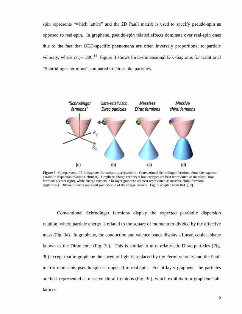
Figure 3 shows three-dimensional E-k diagrams for traditional
“Schrödinger fermions” compared to Dirac-like particles.
Figure 3. Comparison of E-k diagrams for various quasiparticles. Conventional Schrodinger fermions show the expected
parabolic dispersion relation (leftmost). Graphene charge carriers at low energies are best represented as massless Dirac
fermions (center right), while charge carriers in bi-layer graphene are best represented as massive chiral fermions
(rightmost). Different colors represent pseudo-spin of the charge carriers. Figure adapted from Ref. [10].
Conventional Schrodinger fermions display the expected parabolic dispersion
relation, where particle energy is related to the square of momentum divided by the effective
mass (Fig. 3a). In graphene, the conduction and valence bands display a linear, conical shape
known as the Dirac cone (Fig. 3c). This is similar to ultra-relativistic Dirac particles (Fig.
3b) except that in graphene the speed of light is replaced by the Fermi velocity and the Pauli
matrix represents pseudo-spin as opposed to real-spin. For bi-layer graphene, the particles
are best represented as massive chiral fremions (Fig. 3d), which exhibits four graphene sub-
lattices.

7
In either single or bi-layer graphene, the electron energy bands (pink) and hole energy
bands (blue) are three-fold degenerate at the two unique points of the sub-lattice (A and B),
leading to six equivalent Dirac cones (differing only by pseudo-spin) that meet at the six
corners of the two-dimensional, hexagonal Brillouin zone as shown in Figure 4.15
Figure 4. Three- dimensional band structure of graphene showing the six Dirac cones in the first Brillouin zone. Adapted
from Ref. [15].
The meeting point between the two energy bands in k-space occurs at the Fermi
energy of graphene (zero-energy) and represents a vanishing density of states. The vanishing
density of states can also be thought of as a zero energy bandgap; and, for this reason,
graphene is often referred to as either a zero-bandgap semiconductor or semi-metal.
Although such a band structure suggests extremely high resistance at this zero-energy point,
random thermal fluctuations and deformations of the graphene sheet lead to the generation of
both electrons and holes and the formation of electron-hole puddles which result in a
universal minimum conductivity ranging between 4e2/h to 8e
2/h (5.8 – 2.9 k) depending on
the intrinsic impurity concentration.16
8
Besides pseudo-spin, charge carriers in graphene can also be described by another
quantity, which is termed chirality. Chirality, or handedness, can be thought of as the
projection of the 2D Pauli matrix onto the direction of motion and is positive for electrons
and negative for holes. The combination of pseudo-spin and chirality are important for
understanding many of the phenomena of graphene, such as Klein tunneling.
1.2.3.2 – Electronic Transport Properties
Although graphene’s novel Dirac like particles and structure have been the focus of
many works, arguably it is the exceptional electronic transport properties, even at room
temperature and high carrier concentrations, that have been the highlight of application
focused research. This is because the high crystalline quality of graphene samples and
unique band structure of the material leads to extremely fast conduction of charge carriers,
where mobilities greater than 200,000 cm2/Vs have been reported for suspended samples in
vacuum and at low temperatures17
and values of 10,000 – 15,000 cm2/Vs are routinely
reported for exfoliated samples on SiO2 at room temperature.4,18
These large mobilities lead
to extremely long mean free paths for charge carriers and might allow for room temperature
ballistic transport in graphene-based devices. Moreover, electron’s and hole’s demonstrate
nearly symmetric transport properties as a result of the symmetry of the Dirac-cone about the
zero energy point (Fermi energy). Figure 5 plots resistivity of graphene as a function of gate
bias (Fermi level), showing nearly symmetric hole- and electron-branches. E-k diagrams
inset into the figure show the semi-metal transition across the Dirac point.

9
Figure 5. Resistivity of graphene as a function of back gate bias (carrier concentration) showing symmetric electron and
hole-branches. Adapted from Ref. [15].
Additionally mobilities appear to be weakly dependent on temperature, indicating that
transport is likely limited by remote charged impurity scattering and suggesting that these
values may yet be improved. Importantly, mobilities remain high up to carrier
concentrations on the order of 1013
carriers/cm2 and carrier concentrations can be easily
tuned between electrons and holes through electrical gating or chemical doping. Besides
high mobilities, graphene also demonstrates high saturation velocity, with values up to 3x10⁷
cm/s measured for graphene on SiO2 at low carrier concentrations19
and theoretical
predictions of 4.6x107 cm/s for full-band Monte Carlo simulations of intrinsic graphene,
20
and an extremely high current carrying capacity, with current densities as high as 108 A/cm
2
reported for graphene nanoribbons with widths on the order of 20 nm.21
These properties far
surpass typical semiconducting materials. Table 1 lists the bandgap, electron/hole mobility,
thermal conductivity and intrinsic carrier concentration of several common semiconductors
compared to graphene, where graphene excels in both carrier mobility and thermal
conductivity.

10
Table 1. Bandgap, mobility, thermal conductivity, and intrinsic carrier concentration of common semiconductors as
compared to graphene. 22 Data sourced from Ref. [22].
material
band gap
(eV)
electron
mobility
(cm2 V
-1 s
-1)
hole
mobility (cm2
V-1
s-1
)
thermal
conductivity
(W cm-1
K-1
)
intrinsic carrier
concentration
at 300K (cm-3
)
Si 1.12 1,400 450 1.3 1.10 x 10¹⁰
Ge 0.66 3,900 1,900 0.58 2.0 x 10¹³
GaN 3.39 1,000 200 1.3 3.4 x 10¹⁰
SiC
(4H/6H) 3.23/3.0 900/400 120/90 3.7/4.9 ~1 x 10
-5
Diamond 5.46-5.6 2,200 1,800 6-20 ~1 x 10-27
GaAs 1.42 8,500 400 0.55 2.1 x 10⁶
InAs 0.35 40,000 500 0.27 1 x 10¹⁵
Graphene 0-0.2 200,000 200,000 48-53 ~2.7 x 10¹⁶
Considering graphene’s excellent electronic transport properties in combination with
its near symmetric ambipolar conduction of both holes and electrons and unique Dirac-like
description of charge carriers, it’s easy to understand the great excitement generated by this
amazing material since its discovery.
1.2.4 – Synthesis of Graphene
Although the initial discovery of graphene was ground breaking in establishing the
stability of two-dimensional crystals, the synthesis technique used to produce those first
samples could be considered somewhat inelegant. The technique, referred to as exfoliation,
relies on micro-mechanically cleaving two-dimensional crystals from a three-dimensional

11
graphite bulk by physically dragging highly-ordered pyrolitic graphite (HOPG) across a
substrate5 or by peeling off graphene layers using scotch tape.
4 The process of exfoliation
produces high-quality graphene crystallites up to 10 m long, but simultaneously produces
bi-layer and multi-layer crystallites as well. Because of the various types of crystallites
produced during exfoliation, optical microscopy must be utilized to search out and identify
single-layer graphene crystallites for further processing or testing. Although exfoliation
produces crystallites of extremely high crystallinity that demonstrate excellent electronic
properties, the technique is decidedly time consuming and impractical for wide-scale
manufacturing. Synthesis by mechanical cleavage has become more efficient in recent years,
even incorporating the use of ultrasonication to create suspensions of sub-micron graphene
crystals which can be used to coat arbitrary substrates,23
but the introduction of new synthesis
techniques such as CVD or sublimation have allowed for wafer scale synthesis of large-
grained, polycrystalline graphene films and have provided promise for the eventual
commercialization of graphene-based electronic technologies that require high quality,
affordable graphene substrates.
1.2.4.1 – Chemical Vapor Deposition on Metals
The synthesis of graphene by chemical vapor deposition (CVD) on metal substrates
has proven to be an excellent large-scale growth technique. Although this technique has
been known to produce thin carbon films for more than 40 years, it was not until the
discovery of free standing graphene and its phenomenal properties that CVD growth of
carbon films became an important focus of many researchers.
When discussing synthesis of graphene on metals by CVD, there are two separate
methods that must be considered: first, the method of segregation of bulk-dissolved carbon
12
at the surface24
and, second, the method of surface decomposition of carbon-containing
precursors.25
For the first technique, carbon must first be dissolved into the metal substrate
before segregation can occur. Carbon dissolution can be achieved by keeping the sample in
contact with a graphite source at elevated temperatures as well as other techniques, as
summarized in Ref [23]. Segregation takes place as the metal is cooled and temperature as
well as cooling rate can be used to control the synthesis and morphology of the resulting
graphene film. For the second technique, surface decomposition, graphene synthesis occurs
by decomposition of one of various precursors, including methane, propene, ethylene, and
others, onto a metal substrate at high temperatures (1000 C). In both the segregation and
decomposition techniques, transition metals such as Cu, Ni, Ru, or Ir are used as the substrate
for graphene synthesis. The success of the technique comes from the fact that the growth
process is self-limiting and controllable, where the growth of a single- or few-layer carbon
film halts further segregation/deposition of carbon onto the metal substrate and temperature
and concentration/partial pressure can be manipulated to controllably produce monolayer or
few-layer films.
Although both techniques are found to produce continuous sheets of graphene, often
with large domains regardless of the crystalline quality of the underlying metal, the use of a
conductive metal substrate complicates device fabrication when considering graphene for
electronic applications. In order to make CVD deposited graphene technologically viable,
transfer26,27
and transfer-free28
processes have been developed in the past few years, where
CVD graphene can be relocated onto an insulating substrate for subsequent device
fabrication. In these processes, graphene films are usually bonded to a temporary substrate,
often a simple polymer film that can be spun on top of the CVD graphene. The temporary
substrate is then used to support the monolayer as it is removed from the metal substrate and
13
transferred onto an insulating substrate. After transfer, the temporary substrate can be etched
away to leave only the graphene on top of its insulating substrate.
1.2.4.2 – Sublimation of Si from SiC
Unlike CVD based synthesis techniques, growth of graphene by sublimation of Si
from SiC requires no transfer step. Instead, the technique produces a thin carbon film on top
of a semi-insulating SiC substrate that allows for subsequent device processing. Silicon
sublimation occurs at high temperatures (~1400-1600 C) and can take place either in ultra-
high vacuum or in an argon atmosphere. The use of argon during the sublimation process
can help to improve film morphology, leading to reduced pitting and much larger domain
sizes than achievable using high vacuum sublimation.29
Additionally, SiC substrates are
often subjected to a hydrogen etch before the sublimation step, which takes place at elevated
temperatures (>1500 C). The use of a hydrogen etch prior to graphene synthesis is effective
in removing much of the residual surface damage caused by SiC polishing techniques and
promotes growth of large grains. Importantly, the hydrogen etch also leads to significant
step-bunching and the formation of terraces across the SiC surface.30
Terrace formation
exposes the (110n) crystallographic plane of the SiC at the step-edge, as shown in Figure 6,
which has important implications for the graphene morphology on the Si-face of the
substrate.

14
Figure 6. Schematic cross-section showing the crystallographic planes of a SiC substrate after a hydrogen etch. Adapted
from Ref. [31].
Both 4H- and 6H-SiC crystals can be used for synthesis, with graphene growing on
both the (0001) (silicon-terminated) and (0001) (carbon-terminated) crystal faces. The two
unique crystal faces exhibit different growth modes, which produce very different graphene
films. Graphene produced by sublimation of Si from SiC is referred to as epitaxial graphene,
or EG, where Si-face EG is designated as EGSi and C-face EG is designated as EGC.
Growth on the Si-face (0001) produces single- or few-layer graphene which exhibits
the same Bernal stacking found in bulk graphite. Because of its Bernal stacking, Si-face
epitaxial graphene may also be referred to as few-layer graphite, or FLG. Although growth
on the Si-face is self-limited and highly controllable down to a single monolayer of graphene,
the presence of step-edges across the substrate surface lead to regions of multi-layer
graphene interspersed between few-layer regions. This phenomenon is a result of the fact
that graphene growth on the (110n) crystal face differs from the (0001) face, where growth
on the (110n) face occurs at lower temperatures and is not self-limiting. This can lead to
multi-layer regions of graphene at step edges, as shown in Figure 7.

15
Figure 7. Cross-sectional TEM micrograph (a) showing the growth of multi-layer graphene on the (11 0n) crystal face (c),
while graphene growth on the (0001) crystal face is limited to single- or bi-layer graphene (b). Adapted from Ref. [31].
It is thought that step-edges serve as nucleation sites for the graphene film due to their
high density of dangling bonds and defective nature. 31
Figure 8 shows a cross-sectional
TEM micrograph of a step-edge that shows multi-layer graphene growth along the (110n)
crystal face while the (0001) terrace ledges show no graphene indicating that the (110n) face
serves as a nucleation site for graphene growth.
Figure 8. Cross-sectional TEM micrographs of graphene nucleated on the terrace step edge of SiC at 1325 C. Many-layer
graphene is possible along the (11 0n) plane and can occur before growth of graphene on the terrace face (0001). Adapted
from Ref. [31].

16
Along the (0001) crystal face, EGSi layers are strongly bound to the substrate by
means of a carbon buffer layer, which induces strong doping and significant spectral disorder
at low energies near the Dirac point.32,33
Away from the Dirac point (at higher energies) Si-
face epitaxial graphene display’s the typical linear dispersion relation of graphene.32
Mobilities for Si-face epitaxial graphene were initially much lower than C-face epitaxial
graphene, CVD graphene, and exfoliated graphene, but are now approaching the values
found in CVD graphene (~3000 cm2/Vs). The limited mobility of Si-face epitaxial graphene
is likely due partially to the presence of the carbon buffer layer.
Along with the problem of multi-layer regions of graphene as a result of step-
bunching across SiC substrates, reduced mobility of EGSi samples remains an issue for high
performance graphene devices using Si-face epitaxial graphene. Recent work to cleave EGSi
from the carbon buffer layer by hydrogen intercalation has led to substantial improvements in
electronic transport properties as well as reduced doping,34
suggesting that passivation or
removal of the buffer layer is integral to high performance EGSi.
As opposed to growth on the Si-face, growth on the C-face occurs rapidly and with
little control, producing multi-layer graphene that exhibits a mix of rotationally faulted and
Bernal stacked layers of graphene.35
Graphene layers that are rotationally faulted are referred
to as turbostratic graphene. C-face graphene, in contrast to graphene produced on the Si-face
and before passivation of the buffer layer, exhibits little doping and exceptional electronic
quality due to its more free-standing nature from the SiC substrate. The improved isolation
of C-face graphene is attributed to weak electronic coupling between the rotationally faulted
layers in combination with shielding by the outermost graphene layers.36
The interface
between graphene and the C-face of the SiC substrate is less understood than on the Si-face.
Although the weak coupling between layers promotes high mobilities, it also limits
device applications. This is because external electric fields are effectively screened by only a

17
few layers of graphene, leaving the additional layers as shunt conducting channels that
reduce device performance. Controlled growth of few or mono-layer graphene on the C-face
could circumvent this problem, but, at this time, such highly controlled growth has not been
possible.
1.3 – Graphene Field-Effect Transistor
The metal-oxide-semiconductor field-effect transistor (MOSFET) is the building
block of modern integrated circuits and dynamic memories. Figure 9 shows the basic
structure of the MOSFET, a four-terminal device with terminals designated as gate, source,
drain, and body. The basic function of the MOSFET is to act as a switch, which can be
suited for various electronic applications ranging from digital logic to high-frequency analog
applications.
Figure 9. Schematic cross-section of basic MOSFET structure.
The MOSFET operates by use of the field-effect, where an appropriate voltage
applied to the gate terminal is used to modulate the conductivity of the transistor by forming
Source
Contact
Gate
Contact
Gate
Dielectric
Substrate
Drain
Contact
Channel Length

18
a conductive channel between the source and drain terminals that puts the transistor into an
on state. Without appropriate bias to the gate, the channel remains resistive and the transistor
exists in an off state, or non-conducting state. In the conventional MOSFET, semiconductors
such as silicon, gallium arsenide, indium phosphide, and gallium nitride, among others, can
be utilized to form the channel of the device, where the unique ability of semiconductors to
modulate their conductivity over several orders of magnitude makes them appropriate for
switching applications. The different material and electronic properties of the various
semiconductors make them suitable for specific applications.
Graphene’s exceptional electronic properties have made it of great interest for
electronic applications; and, although not truly a semiconductor, the graphene-based field-
effect transistor, or GFET, has received considerable attention. This is likely due in part to
the increasing challenges facing the IC industry as it attempts to continuously scale the
silicon transistor, such as increased short channel effects or the increasing dominance of
parasitics in device operation. It is these challenges that have lead the IC industry to seek out
alternative, post-silicon materials that offer better performance or new opportunities to
overcome these challenges. Another reason for interest in the graphene FET is its potential
to outperform conventional semiconductors. Graphene offers not only high electron and hole
mobilities and a large saturation velocity, but is the ultimate two-dimensional material, being
only one monolayer thick. This two-dimensionality may represent the ideal platform for
controlling short channel effects in ultra-scaled devices. Together, these attributes have
attracted much initial interest in graphene-based FETs, but there exist significant challenges
to the success of such a device in either digital or analog applications.
For the graphene-based FET to be successful in digital applications, the engineering
of a bandgap is paramount. Without a bandgap, the semi-metal graphene will not be able to
achieve the on-off ratios necessary to be a viable replacement for silicon logic devices.
19
Fortunately, several solutions have been suggested for the formation of an electronic bandgap
in graphene, including the application of a transverse electric field to bi-layer graphene,37
utilization of strain,38
or the confinement of large-area graphene to form one-dimensional
graphene nanoribbons,39
although the exact origin of the band gap in graphene nanoribbons is
still under debate. Despite the difficulty of bandgap engineering in graphene transistors,
several experimental demonstrations of GFETs with room temperature on-off ratios ranging
from <2 to 100 have been successfully realized using single-layer graphene, bi-layer
graphene, and graphene nanoribbons. Still, these on-off ratios are several orders of
magnitude lower than that required for digital applications as defined by the International
Technology Roadmap for Semiconductors (>104) 40
and further work remains to advance
graphene to the point where it might be a viable alternative to Si-based CMOS.
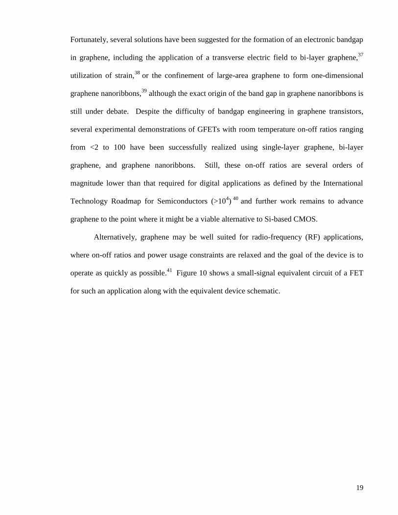
Alternatively, graphene may be well suited for radio-frequency (RF) applications,
where on-off ratios and power usage constraints are relaxed and the goal of the device is to
operate as quickly as possible.41
Figure 10 shows a small-signal equivalent circuit of a FET
for such an application along with the equivalent device schematic.

20
(a)
(b)
Figure 10. Schematic diagram of typical FET showing parasitic resistances and capacitances (a) and equivalent small-
signal model (b) adapted from Ref [41].
Transistor RF performance is dependent on maximizing the gain and reducing
parasitics of the small-signal circuit, where Equation (3) relates the device parameters to the
small-signal current gain cut-off frequency (fT).42
(3)

21
The small signal cut-off frequency represents the maximum switching frequency of
the FET and is defined as the frequency at which the magnitude of the small-signal current
gain becomes unity.42
Cut-off frequency, along with Mason’s Invariant and other
parameters, is often used as a figure of merit to evaluate the performance of RF technologies.
In this way, shorter channel lengths (smaller C), higher mobilities (higher gm), and reduced
series resistances (RD, RS) all lead to increased RF performance (higher fT).
With its excellent possibility for scaling to sub-20 nm gate lengths,43
high
transconductance44 , 45
and sufficiently low noise level,46
graphene could be an excellent
candidate for RF electronics that operate into the THz regime.47
To this end, researchers
have demonstrated graphene based RF FETs47, 48 ,49
and have utilized them in low-noise
amplifiers,50
frequency mixers,51,52
and frequency multipliers53
only a few years after the first
reported graphene FET.54
Although graphene transistors in recent years have reached an
impressive intrinsic current gain cut-off frequency (fT) of 300 GHz,55
the extrinsic
performance of RF GFETs has lagged behind intrinsic performance, with the highest
reported extrinsic fT (~30 GHz) over an order of magnitude smaller than the highest reported
intrinsic fT (300 GHz).
The difference in extrinsic and intrinsic performance of graphene FETs is a direct
result of device parasitics. Parasitic resistances in the form of contact resistances (RC) or un-
gated portions of graphene combine to create high access resistances (RS, RD) that degrade
RF performance. Additionally, un-optimized device designs might lead to unacceptably high
parasitic capacitances. Along with device parasitics, the limited saturation behavior
demonstrated by graphene devices and the in-ability to integrate top-dielectrics without
degradation of transport properties in the underlying graphene combine to limit the ultimate
achievable RF performance of graphene FETs by leading to high gd and reduced mobility
(low gm). In order to push graphene-based technologies forward, metal-graphene contacts
22
and top-gate dielectrics on graphene must be better understood and optimized. Additionally,
the weak-saturation of graphene devices, device processing, and short-channel effects in
graphene FETs must also be better understood.
1.3.1 – Metal-Graphene Contact
To-date the focus of electronic and opto-electronic graphene research has been to
push speed and sensitivity to the extreme;56,57,58
however, little attention has been given to a
potentially limiting factor in one’s ability to extract the phenomenal properties of graphene:
the metal-graphene contact. Of the studies that investigate contact resistance to graphene, the
lowest reported resistances are on the order of 5x10⁻⁶
ohm-cm2,59,60,61,62,64,
Although, specific
contact resistances of 10-7
ohm-cm2 have been reported for Ti/Pt/Au contacts to epitaxial
graphene,63
limited explanation was provided as to how these low values were achieved.
Yet, in order to push graphene-based RF transistor operating speeds into the near terahertz
regime, device scaling will require ohmic contacts exhibiting a specific contact resistance <
1x10⁻⁹
ohm-cm2.64
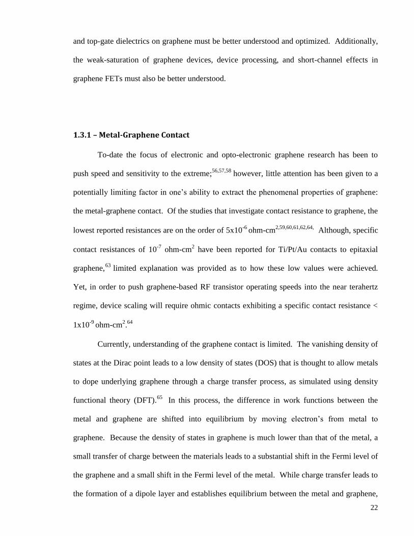
Currently, understanding of the graphene contact is limited. The vanishing density of
states at the Dirac point leads to a low density of states (DOS) that is thought to allow metals
to dope underlying graphene through a charge transfer process, as simulated using density
functional theory (DFT).65
In this process, the difference in work functions between the
metal and graphene are shifted into equilibrium by moving electron’s from metal to
graphene. Because the density of states in graphene is much lower than that of the metal, a
small transfer of charge between the materials leads to a substantial shift in the Fermi level of
the graphene and a small shift in the Fermi level of the metal. While charge transfer leads to
the formation of a dipole layer and establishes equilibrium between the metal and graphene,

23
it is thought that charge redistribution is also impacted by a metal-graphene chemical
interaction, which may have a significant repulsive contribution.65
Figure 11 compares the
DOS and energy band diagrams of metal contacts to graphene versus other materials.
Figure 11. Comparison of DOS and energy band diagrams for graphene and carbon nanotubes (CNT), and conventional
Schottky contacts to silicon. Adapted from Ref [66]
In graphene, limited DOS at the Dirac point combined with the lack of a bandgap
leads to a charge transfer to the graphene from the metal. In metallic carbon nanotubes
(CNT), the higher density of states prevents any shift in the energy diagram as the CNT is
able to absorb electrons without a large shift in the Fermi level. For the case of the
semiconductor CNT, the CNT remains charge neutral, although the ratio of holes to electrons
changes as the metal and CNT are brought into contact. This behavior is very similar to the
case of the conventional metal-semiconductor contact, where the Fermi level shifts within the
bandgap but there is no net accumulation of charge.

24
Although DFT results suggest that doping of graphene by metal contacts can be
predicted using a simple analytical model,65
experimental graphene devices offer
significantly more complex material systems as opposed to a simple metal-graphene junction
and may not always exist at the Dirac point. For instance, the presence of a carbon buffer
layer between at the substrate-graphene interface for the case of EGSi leads to extensive
doping of the graphene, which alters the work function difference between the metal and
graphene and leads to a much higher DOS in the graphene. Additionally, impurities and the
presence of defects or thin layers of contamination between the metal and graphene might
lead to a dramatic change in the difference between the two material’s work functions by
altering the graphene metal spacing and the dipole interaction at the metal-graphene
interface.41,65, 66
Additionally, contact-induced strain or process dependent
chemisorptions/physisorption differences may lead to a change in the effective work function
at the metal-graphene interface.66
These complications have led to experimental results that have not shown good
agreement with predicted results. Particularly, Raman spectroscopy was used to show the
appropriate correlation of G-peak with work function of metal contacts on graphene (where
the G-peak exhibits a dependency on the Fermi level), but the carriers induced in the
graphene did not match the predicted work function difference.66
These results indicate that
the ideal work functions of the metals might not be accurate for the case of metals on
graphene. Additionally, the interesting results of substrate modulated contact resistance in
double-gated graphene FETs (top- and back-gated) also point to complexities at the metal-
graphene interface and provide evidence for an altered energy dispersion at the metal-
graphene interface67
or the presence of a thin effective dielectric interfacial layer at the metal-
graphene interface that capacitively couples the graphene to the contacts.68
25
1.3.2 – Dielectric-Graphene Interface
Within the GFET, the dielectric acts as an insulating spacer that capacitively couples
the metal gate to the graphene channel, allowing the channel, and thus the transistor output,
to be modulated. In this way dielectrics are a fundamentally essential component of the
GFET and must serve several roles. First, the dielectric stack mustn’t degrade the underlying
graphene structurally or reduce carrier mobility as to limit device performance. Second, the
dielectric must isolate the channel and gate sufficiently to prevent leakage currents and
should be robust and resistant to breakdown. Third, the dielectric should provide a good
electrical interface at the graphene channel and not introduce significant amounts of fixed
charge, mobile oxide charge, or interface states as to reduce the performance of the graphene
FETs. Finally, the gate stack should effectively couple the metal gate to the channel and
should be thin with respect to the channel length in order to reduce short channel effects.
In fabricating the graphene FET, various techniques have been used to implement
top-gate dielectrics, including electron-beam physical vapor deposition (EBPVD),69 , 70
functionalized atomic layer deposition (ALD),71,72,73
and seeded ALD (either through use of a
thin oxidized metal layer74,75
or a polymer buffer layer76
). Additionally, physical assembly
techniques such as the use of thin alumina nanoribbons77,
or self-aligned oxidized nanowires78
have been employed with success, although the extent to which these techniques are scalable
is not clear.
While current implementations of the GFET have shown great promise using these
techniques, top-gate dielectrics often cause an undesirable degradation in the transport
properties of the underlying graphene, often reported as a decrease in carrier mobility.76,79,80
Alternatively, calculations have shown that high dielectric constant (high-) materials should
have the effect of suppressing charged impurity scattering in the underlying graphene leading
26
to an increase in carrier mobility.81,82
Such an increase in carrier mobility has been shown
variously by increasing the dielectric constant of a solvent overlayer83,84
or by use of an ice
overlayer,85
but increase in carrier mobility with deposition of high- dielectric by
conventional means such as EBPVD, chemical vapor deposition (CVD), or ALD has yet to
be experimentally demonstrated.
1.3.2.1 – Physical Vapor Deposition of Dielectrics on Graphene
PVD techniques, such as EBPVD, pulsed laser deposition (PLD), spin-coating or
sputtering are all suitable techniques for the deposition of thin oxide films. These techniques
rely on physical processes such as thermal evaporation or sputtering to transfer source
material to the substrate in order to deposit a thin film in a non-reactive or reactive
environment. Although these techniques can be used to deposit dielectrics of various
compositions on arbitrary substrates, including graphene, the physical processes used can
often cause significant damage to the underlying substrate onto which the dielectric is
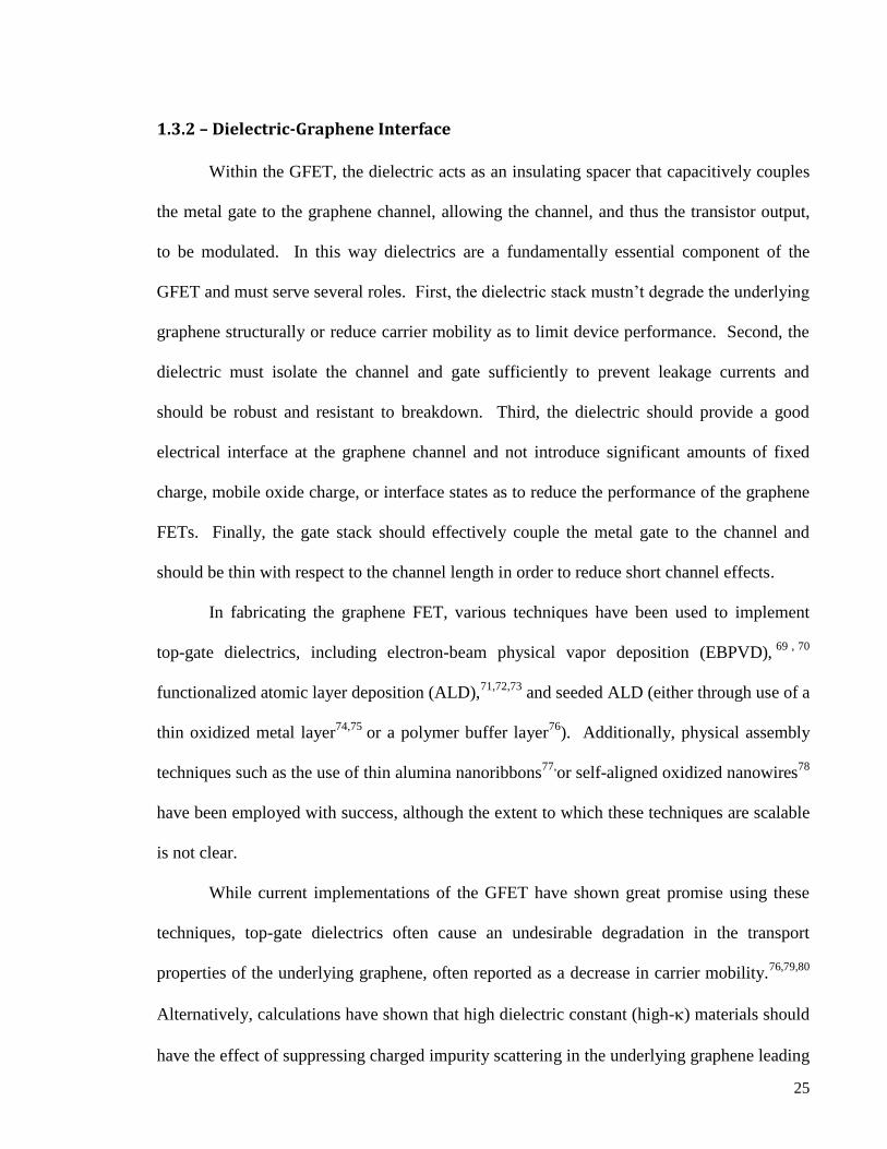
deposited. Using Raman analysis of graphene after depositing a layer of SiO2 by various
PVD techniques, Figure 12 shows the extent of structural damage caused by the various
processes.86

27
Figure 12. Raman spectra of exfoliated graphene samples post-dielectric-deposition by various PVD techniques where D-
peak intensity represents extent of structural damage. Adapted from Ref [86].
Raman analysis is used to compare the relative damage introduced by the various
techniques by comparing the intensities of the D and G-peaks in the graphene Raman
signature. A large D/G ratio indicates a large degree of structural disorder, which is
indicative of a highly damaging deposition process. Of the PVD techniques, spin coating and
EBPVD lead to the smallest change in the magnitude of the D/G, indicating minimal
incorporation of defects or structural damage in the underlying graphene. The deposition of
oxides by PLD and RF sputtering, on the other hand, leads to significant increase in the D/G
ratio and even leads to a quenching of the 2D peak (Raman signature produced by pristine
graphene). The significant increase in graphene defectiveness for these two techniques leads
to a degradation in the electronic transport properties of the underlying graphene and
precludes their use for the deposition of gate dielectrics for graphene based electronics.
Although spin-coating is found to be the least damaging PVD process, the technique is
suitable only for the deposition of dielectrics that can be spun onto graphene in liquid form.
28
Unfortunately, this requirement means that spin-coating is unsuitable for the deposition of
high- dielectrics, which will allow for better control of short channel effects and have the
potential of improving transport properties by reducing remote charged impurity scattering.
Alternatively, a thin layer of low- dielectric deposited by a spin-on process can be
used as a seed layer for subsequent deposition of dielectrics by another approach. The seed
layer can be thought of as a buffer against physically damaging processes. Still, the use of a
low- seed layer acts to increase the equivalent oxide thickness (EOT) of the dielectric stack
and might prevent high- dielectrics from screening out remote charged impurity scattering,
which are both undesirable for high performance GFETs.
1.3.2.2 – Atomic Layer Deposition of Dielectrics on Graphene
Atomic layer deposition (ALD) is a well developed technique for depositing
dielectrics with a high degree of control over film thickness. Additionally, the technique can
be used to deposit ultra-thin dielectrics. ALD is a CVD-based process that relies on
sequential use of two gas phase precursors that are fed into a reactor in short pulses. The
precursors react to deposit a single mono-layer of the desired material in a self-limiting
process. After each sequential deposition of a new mono-layer, the reaction chamber is
purged before the next precursor is supplied. In this way, purge gases and precursors are
supplied to the reaction chamber, which is often at elevated temperature, in order to deposit a
compound sequentially, layer by layer.
Deposition of dielectrics by H2O-based ALD onto pristine graphene is complicated
by the hydrophobic nature of the graphene surface87
and the lack of any functional groups
that might allow for the molecular absorption of the gas precursors. Instead of uniform and
29
conformal dielectric thin films, attempts to deposit dielectrics by ALD onto pristine graphene
lead to selective growth at steps between graphene layers or defects, such as pentagon-
hexagon pairs or vacancies, while most of the surface remains uncoated.88
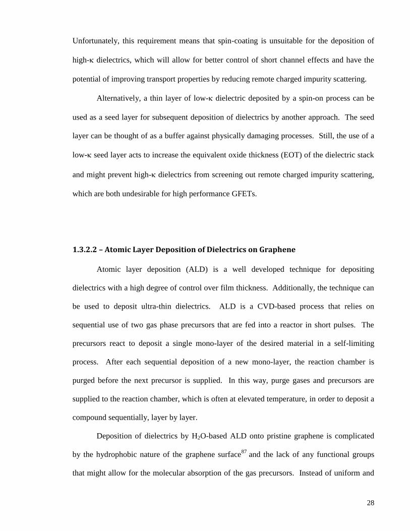
Figure 13 shows
atomic force microscopy (AFM) micrographs of exfoliated graphene before and after
deposition of ALD deposited Al2O3.
Figure 13. AFM micrographs of few-layer exfoliated graphene sample before (a) and after (b) deposition of ALD deposited
Al2O3. (b) shows that the nucleation and growth of the Al2O3 film occurs only at steps in the graphene or at localized
defects. (c) and (d) are schematic cross-sections of the samples. Adapted from Ref [88].
Figure 13b clearly shows the nucleation of dielectric growth along graphene edges
and defects. The nucleation process is schematically illustrated in Figure 13c,d. In order to
promote molecular absorption and, hence, dielectric growth over the graphene surface,
surface functionalization of the graphene can be used to create additional functional groups
for dielectric nucleation.89
To this end, chemical functionalization has been employed using
either NO2-TMA (trimethylaluminum)72
or O3, 71
which is flown into the reactor before
30
dielectric deposition. Although these techniques lead to uniform thin films <10 nm thick and
without any pinholes, the use of chemical functionalization also produces an undesirable
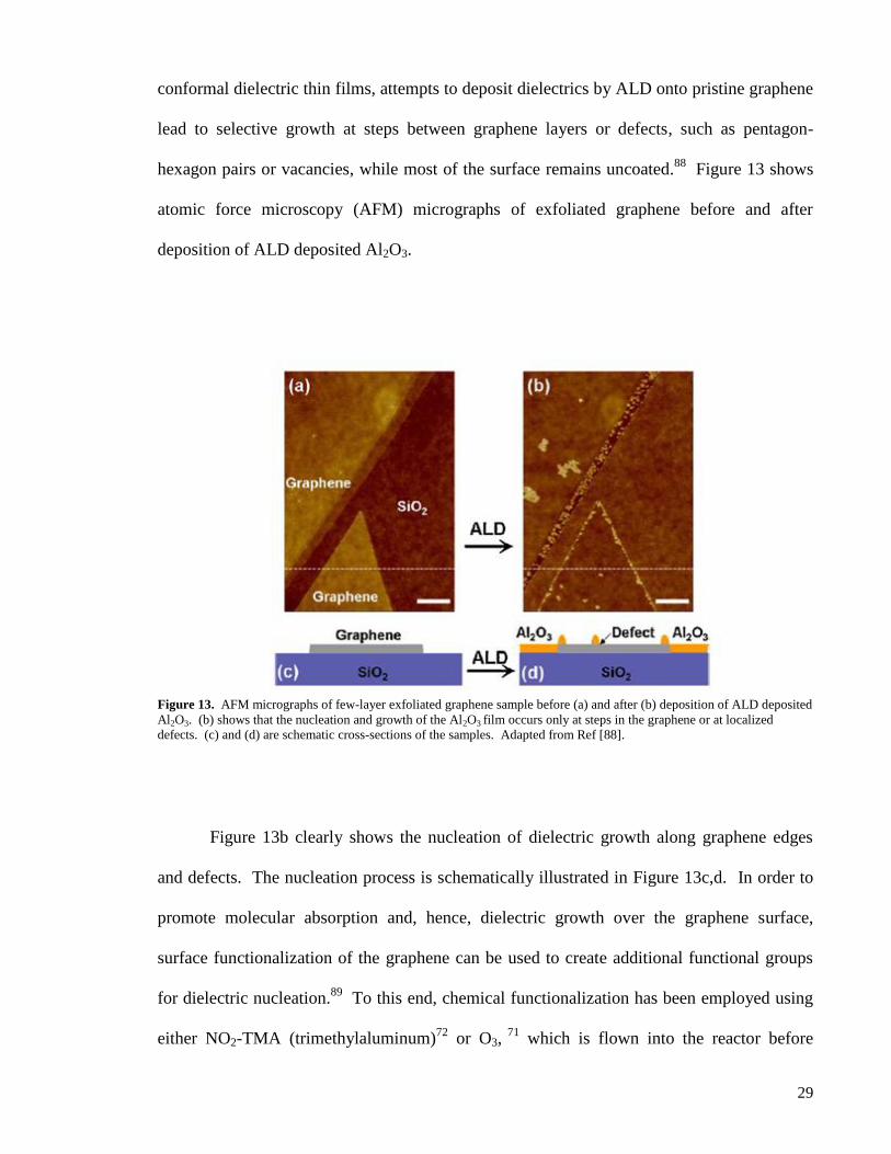
degradation in the transport properties of the underlying graphene, as shown in Figure 14.
In Figure 14, an increase in hysteresis and shift in the Dirac point is attributed dually
to the introduction of a significant density of charge traps and a large fixed charge density in
close proximity to the graphene. Additionally, severe degradation of both the on-off ratio
and drive current is observed. This degradation is attributed to a high density of charged
impurities that act to scatter carriers in the channel or, possibly, to interface phonon
scattering from the deposited high- dielectric.
Figure 14. Transfer curve of back-gated exfoliated graphene before (black) and after (red) deposition of top-dielectric by
ALD using a NO2-TMA chemical functionalization, showing degradation in transport properties. Adapted from Ref [72].
Alternative to the use of chemical functionalization to create additional surface
functional groups, the use of thin dielectric layers deposited prior to ALD growth can be used
as a seed layer to promote coverage and uniformity. Seed layers spin-coated onto the
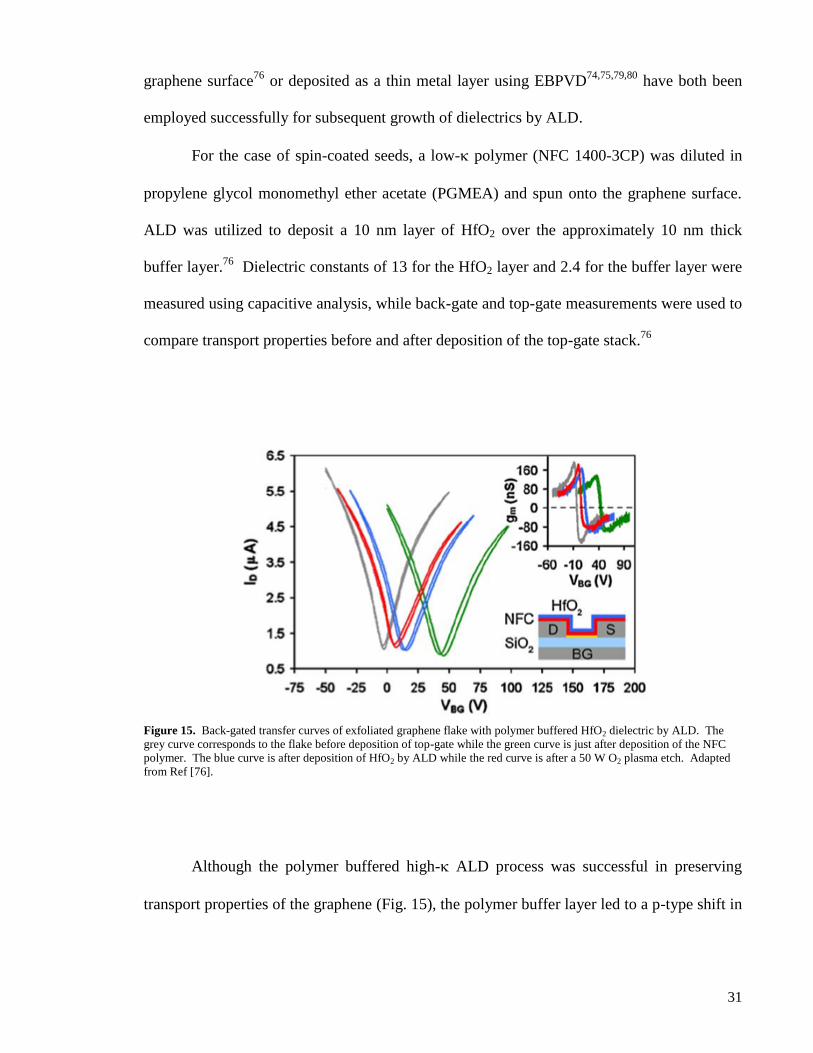
31
graphene surface76
or deposited as a thin metal layer using EBPVD74,75,79,80
have both been
employed successfully for subsequent growth of dielectrics by ALD.
For the case of spin-coated seeds, a low- polymer (NFC 1400-3CP) was diluted in
propylene glycol monomethyl ether acetate (PGMEA) and spun onto the graphene surface.
ALD was utilized to deposit a 10 nm layer of HfO2 over the approximately 10 nm thick
buffer layer.76
Dielectric constants of 13 for the HfO2 layer and 2.4 for the buffer layer were
measured using capacitive analysis, while back-gate and top-gate measurements were used to
compare transport properties before and after deposition of the top-gate stack.76
Figure 15. Back-gated transfer curves of exfoliated graphene flake with polymer buffered HfO2 dielectric by ALD. The
grey curve corresponds to the flake before deposition of top-gate while the green curve is just after deposition of the NFC
polymer. The blue curve is after deposition of HfO2 by ALD while the red curve is after a 50 W O2 plasma etch. Adapted
from Ref [76].
Although the polymer buffered high- ALD process was successful in preserving
transport properties of the graphene (Fig. 15), the polymer buffer layer led to a p-type shift in

32
the graphene.76
Additionally, the low- buffer layer prevented any enhancement of the
graphene transport properties by dielectric screening by the high- ALD dielectric.
EBPVD represents an alternative approach to the deposition of seed layers. Although
EBPVD has been shown to be more damaging then spin-deposited techniques according to
Raman analysis (Fig. 12), the extent of damage is not as great as other PVD processes.
Using EBPVD to deposit a thin layer of metal (1 – 2 nm), several groups have successfully
demonstrated seeded ALD growth of high- dielectrics.74,75,79,80
The advantage of this
technique is that it does not necessitate a low- buffer layer. Instead, a thin metal such as
aluminum can be deposited directly onto the graphene surface using EBPVD. After
removing the metal-coated graphene from the e-beam deposition chamber, the thin metal
layer can be subsequently oxidized to form a high- metal oxide buffer layer, after which
deposition of the bulk dielectric can take place by ALD. This process is referred to as M-
ALD. Figure 16 shows AFM micrographs demonstrating the successful use of M-ALD to
deposit dielectrics on epitaxial graphene using aluminum, titanium, and tantalum metal
seeds.80
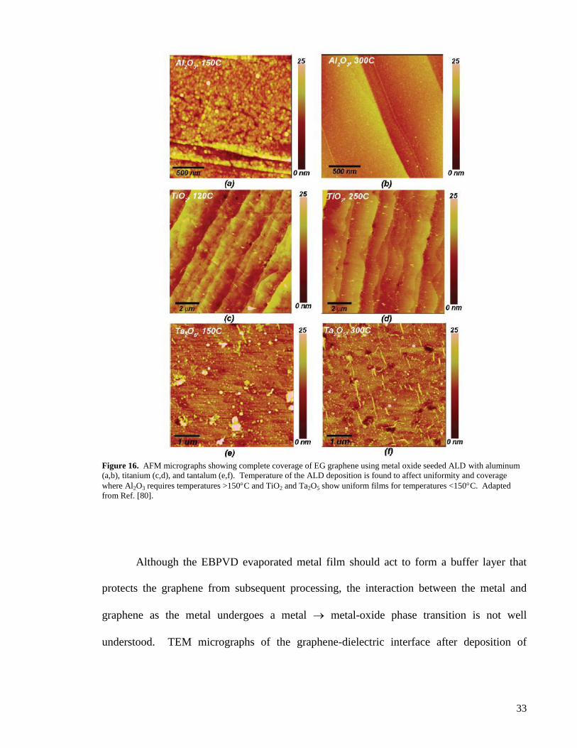
33
Figure 16. AFM micrographs showing complete coverage of EG graphene using metal oxide seeded ALD with aluminum
(a,b), titanium (c,d), and tantalum (e,f). Temperature of the ALD deposition is found to affect uniformity and coverage
where Al2O3 requires temperatures >150C and TiO2 and Ta2O5 show uniform films for temperatures <150C. Adapted
from Ref. [80].
Although the EBPVD evaporated metal film should act to form a buffer layer that
protects the graphene from subsequent processing, the interaction between the metal and
graphene as the metal undergoes a metal metal-oxide phase transition is not well
understood. TEM micrographs of the graphene-dielectric interface after deposition of

34
dielectrics by M-ALD on Si-face epitaxial graphene show that most metal-seeds do not lead
to increased defectiveness from as-grown graphene, Figures 17a, b, c, d.
Figure 17. TEM micrographs of M-ALD deposited dielectrics using various metals (a-d). No significant structural defects
are observed, except for the case of Ta2O5. Raman analysis of the same samples (e) confirms an increase in defectiveness
for graphene coated with a Ta2O5 film deposited by M-ALD. Adapted from Ref [80].
In Figure 17d, Raman analysis shows that negligible change in the D/G ratio occurs
for all dielectrics deposited by M-ALD except for the case of Ta2O5, confirming that most
seeds do not lead to increased defectiveness. On the other hand, the large increase in the D/G
ratio with deposition of Ta2O5 indicates a significant increase in defectiveness, which is
attributed to a large change in the unit cell volume during the metal metal-oxide phase
transition of the M-ALD process (Hf, Al, and Ti phase transitions exhibit smaller volume

35
changes).80
Importantly, this increase in defectiveness has been linked to degraded transport
properties using non-contact mobility measurements, where tantalum seeded dielectrics show
the most severe degradation in mobility over all other seeds.80
No seeds were found to
improve mobility despite theory suggesting the reduction of charged impurity scattering with
high- dielectric overlayer.81,82
Although these results focus on the effects of dielectric
overlayers on the epitaxial graphene system, similar results are found for high-quality
exfoliated graphene samples, where reductions in mobility of 40%76
and ~20%79
have been
reported for samples utilizing oxidized aluminum seeds.
Degradation of transport properties with use of oxidized metal seed despite reports
that metal seeds introduce minimal amounts of disorder into the underlying graphene indicate
that the oxidized metal seed might be a large source of scattering for charge carriers in the
graphene. Additionally, thickness dependent measurements of M-ALD deposited dielectrics
show that graphene mobility decreases as top-gate dielectric thickness is increased.79
These
results suggest the presence of charged defects in the dielectric that act as remote charged
impurity scatterers and lead to reduced mobility. Figure 18 schematically represents this
phenomenon, where point defects such as oxygen vacancies occupy an energy level above
the graphene Fermi level and become charged by injecting an electron into the graphene to
bring the oxide and graphene Fermi levels into equilibrium.
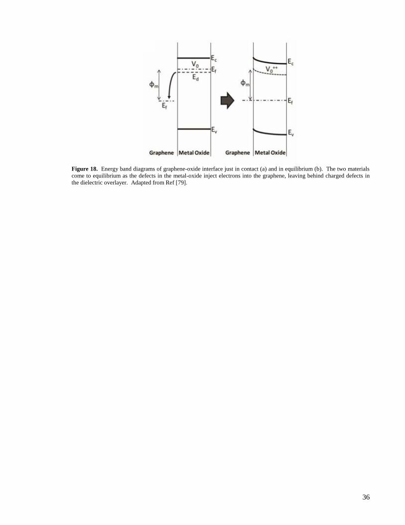
36
Figure 18. Energy band diagrams of graphene-oxide interface just in contact (a) and in equilibrium (b). The two materials
come to equilibrium as the defects in the metal-oxide inject electrons into the graphene, leaving behind charged defects in
the dielectric overlayer. Adapted from Ref [79].

37
Chapter Two: Experimental Plan and Methods
2.1 – Growth
In this work, sublimation was chosen as the synthesis technique. This technique was
utilized to produce Si-face epitaxial graphene. The use of epitaxial graphene allowed for
wafer-scale growth and processing, which, combined with the high degree of thickness
control over EGSi, provided high-throughput, high-yield synthesis and fabrication of
graphene test structures and devices on SiC substrates. A pilot scale physical vapor transport
(PVT) furnace was used for the synthesis process, which utilized inductive heating to reach
temperatures as high as 1900 C. The diameter of the PVT furnaces allowed graphitization
of SiC samples as large as 100 mm diameter wafers.
With such large samples, it was possible to section the samples into multiple regions
that underwent simultaneous processing using different processing techniques or materials.
Using sectioned samples, comparative studies of processing techniques or materials
integration could be performed on a single sample. Alternatively, multiple smaller SiC
samples could be prepared concomitantly in a single graphitization step and then processed
simultaneously using different processing techniques or materials. In this way, the PVT
furnace provided several ways for the preparation of samples and sets of samples that
facilitated comparative studies between different processing techniques or the use of different
materials, such as gate dielectrics.
Graphene synthesis was achieved on the Si-face of semi-insulating 6H-SiC (II-VI,
Inc.) substrates using low-pressure, Ar mediated sublimation at 1600 °C.90
As noted in
Figure 19, an in situ H2 etch was performed by heating the sample to 1600°C in a 5% H2/Ar
mixture at 600 Torr and holding for 60 min.

38
Figure 19. Diagram detailing temperature and pressure during graphitization of SiC wafers.
The use of an in situ H2 etch was effective in removing much of the residual surface
damage caused by SiC polishing techniques and promoted growth of large grains. Figure 20
shows the effect of the hydrogen etch step in removing residual surface damage from the SiC
substrate.
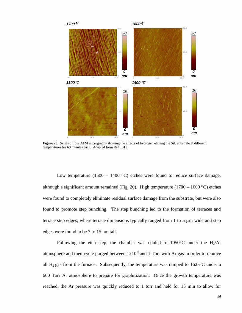
39
Figure 20. Series of four AFM micrographs showing the effects of hydrogen etching the SiC substrate at different
temperatures for 60 minutes each. Adapted from Ref. [31].
Low temperature (1500 – 1400 C) etches were found to reduce surface damage,
although a significant amount remained (Fig. 20). High temperature (1700 – 1600 C) etches
were found to completely eliminate residual surface damage from the substrate, but were also
found to promote step bunching. The step bunching led to the formation of terraces and
terrace step edges, where terrace dimensions typically ranged from 1 to 5 m wide and step
edges were found to be 7 to 15 nm tall.
Following the etch step, the chamber was cooled to 1050°C under the H2/Ar
atmosphere and then cycle purged between 1x10⁻⁶
and 1 Torr with Ar gas in order to remove
all H2 gas from the furnace. Subsequently, the temperature was ramped to 1625°C under a
600 Torr Ar atmosphere to prepare for graphitization. Once the growth temperature was
reached, the Ar pressure was quickly reduced to 1 torr and held for 15 min to allow for
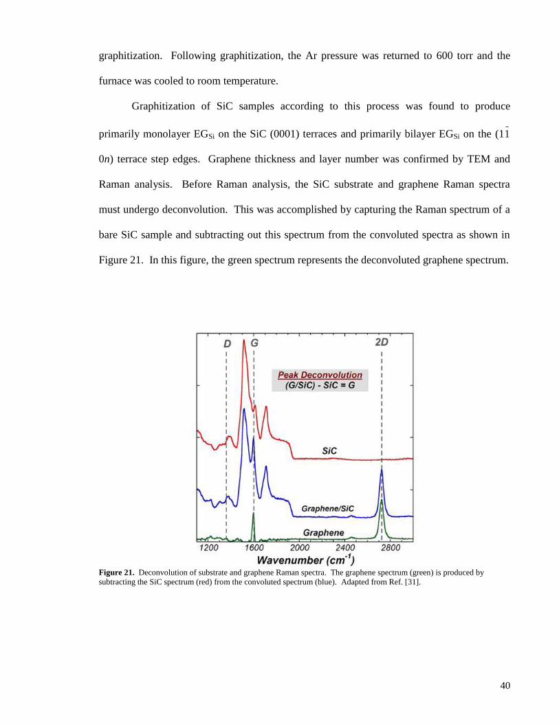
40
graphitization. Following graphitization, the Ar pressure was returned to 600 torr and the
furnace was cooled to room temperature.
Graphitization of SiC samples according to this process was found to produce
primarily monolayer EGSi on the SiC (0001) terraces and primarily bilayer EGSi on the (11
0n) terrace step edges. Graphene thickness and layer number was confirmed by TEM and
Raman analysis. Before Raman analysis, the SiC substrate and graphene Raman spectra
must undergo deconvolution. This was accomplished by capturing the Raman spectrum of a
bare SiC sample and subtracting out this spectrum from the convoluted spectra as shown in
Figure 21. In this figure, the green spectrum represents the deconvoluted graphene spectrum.
Figure 21. Deconvolution of substrate and graphene Raman spectra. The graphene spectrum (green) is produced by
subtracting the SiC spectrum (red) from the convoluted spectrum (blue). Adapted from Ref. [31].

41
After deconvolution, analysis of the graphene 2D peak allows for the determination
of number of graphene layers. As shown in Figure 22a, monolayer and bilayer graphene
exhibit unique 2D peak shapes as compared to bulk graphite (>5 layers of graphene).
Additionally, the two peak shapes differ in the fact that monolayer graphene can be fit with a
single Lorentzian, while bilayer graphene necessitates four Lorentzians. Additionally, a shift
in the 2D peak position from ~2760 cm-1
to ~2730 cm-1
was found when increasing from
monolayer graphene to bilayer graphene. Although TEM micrographs confirmed the
presence of monolayer and bilayer graphene on the (0001) crystal face of the SiC substrates
(Fig. 22b,c), utilization of Raman mapping of the 2D peak position of the as-grown EGSi and
correlating this peak position with the peak fitting, revealed that most of the (0001) terraces
are covered with a single layer of graphene (Fig. 23).
Figure 22. Raman spectra (a) showing the presence of monolayer and bilayer graphene on the SiC (0001) crystal face,
confirmed by cross-sectional TEM micrographs (b) and (c), showing monolayer and bilayer graphene respectively. Adapted
from Ref. [35].

42
Figure 23 shows a Raman map of a typical EGSi Hall cross produced under the
experimental growth conditions, which clearly resolves growth uniformity of the EGSi
graphene over the (0001) terraces. The Raman map plots the 2D peak position as a function
of location across the sample, where the color bar to the right of the map describes the peak
position as function of color.
Figure 23. Raman map of 2D peak position for a EGSi Hall cross structure showing highly uniform growth and strain over
(0001) terraces separated by terrace step edges. Adapted from Ref. [35].
In Figure 23, the red regions displayed a 2D peak position near 2760 cm-1
and were
shown to be comprised mainly of monolayer graphene by correlating the 2D peak position
with a single Lorentzian fit.35
Thus, the monolayer graphene was shown to be uniform over a
majority of the Hall cross using the 2D peak position map. These regions can be described as
an array of wide stripes separated by thin green stripes which run across the surface of the
sample. The thin green stripes displayed a 2D peak position shifted to ~2730 cm-1
and were
shown to be bilayer graphene by correlating the 2D peak position to a four Lorentzian fit.35
43
These bilayer regions comprised a small minority of the Hall cross surface area. The
existence of multilayer graphene across terrace step edges was attributed to the different
growth mode that occurs on terrace step edges, while the presence of step edges was due to
the use of the in situ H2 etch used to remove residual surface damage before graphitization.
2.2 – Materials Characterization
Materials characterization represents an invaluable set of tools for the analysis and
characterization of the as-synthesized and post-processed graphene. Atomic force
microscopy (AFM), scanning electron microscopy (SEM), and transmission electron
microscopy (TEM) were used to evaluate surface morphology and structure of the as-
deposited graphene and gate dielectrics, while Raman spectroscopy was used to evaluate the
quality and thickness of as-grown graphene and to quantify any structural change to the
graphene with deposition of dielectric overlayer. Additionally, x-ray photoelectron
spectroscopy (XPS) was used to evaluate the graphene surface throughout device processing
by determining the surface chemistry of the samples and detecting the presence of
contaminants.
2.2.1 – Atomic Force Microscopy
AFM is a high-resolution scanning probe microscopy which consists of a cantilever
with a sharp tip (probe) as well as a laser and detector. The laser and detector are designed to
measure the amount of deflection of the cantilever as it is scanned across the sample. A

44
piezoelectric tube, or a combination of piezoelectric components, is used to move the sample
in the x, y, and z-directions. Figure 24 shows a simple schematic of an AFM microscope.
Figure 24. Schematic of atomic force microscope showing cantilever, laser and detector, and piezoelectric scanner. The
cantilever is scanned across the sample using a feedback loop to keep the tip at constant force.91 Adapted from Ref. [91].
A Veeco Dimension 3100 AFM system was utilized to acquire all AFM micrographs
in this work. AFM allowed for characterization of dielectric films deposited on graphene by
measuring surface topology. As a characterization technique, it was used primarily to
evaluate surface roughness, conformity, uniformity, and coverage of the dielectrics films.
2.2.2 – Scanning Electron Microscopy
Scanning electron microscopy (SEM) utilizes a high-energy beam of electrons that is
scanned across a sample. As the beam is scanned, electrons are scattered from the sample
and then collected and focused to form an image. Although several imaging modes exist, the
45
primary imaging mode relies on the detection of secondary electrons which are ejected from
the sample atoms by inelastic scattering with the interrogating beam of high-energy
electrons. SEM micrographs offer a very high-resolution image of surface structure and
topology.
A FEI Quanta 2000 scanning electron microscope using a Schottky field emission
gun (FEG) was used to take all SEM images. Although more expensive and time consuming
than AFM, SEM proved to be an excellent technique for observing the as-fabricated device
structure and the condition of the source/drain contacts post-processing.
2.2.3 – Transmission Electron Microscopy
Transmission electron microscopy (TEM) is another type of electron microscopy
which uses a high-energy beam of electrons that are transmitted through an ultra-thin
specimen. The specimen is prepared by mechanical polishing followed by focused ion beam
(FIB) milling. The electrons which pass through the sample interact with the atoms to scatter
and form an image, which is magnified and focused onto an imaging device.
A JEOL 2010F transmission electron microscope was used to take all TEM
micrographs in this work. TEM was utilized to characterize the growth of graphene by
sublimation, by allowing direct observation of the number of graphene layers and any defects
in the substrate or graphene. Additionally, TEM allowed for direct observation of the
dielectric-graphene interface in order to quantify any structural degradation of the graphene
with deposition of dielectric.
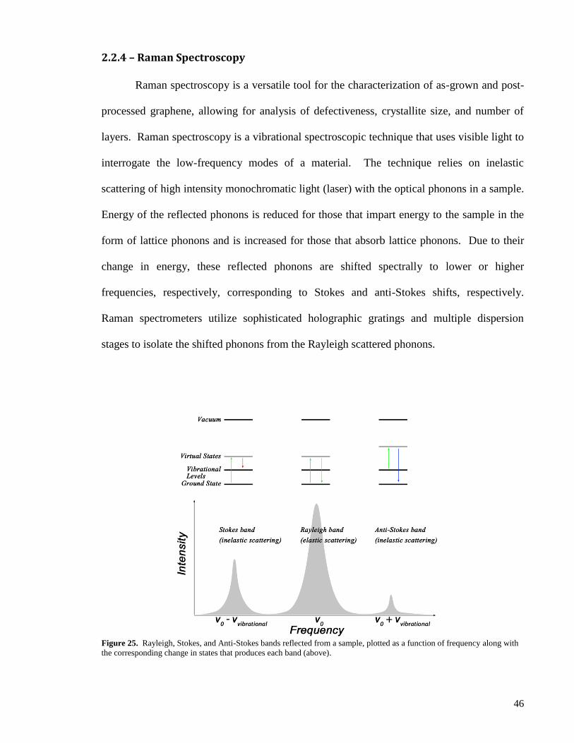
46
2.2.4 – Raman Spectroscopy
Raman spectroscopy is a versatile tool for the characterization of as-grown and post-
processed graphene, allowing for analysis of defectiveness, crystallite size, and number of
layers. Raman spectroscopy is a vibrational spectroscopic technique that uses visible light to
interrogate the low-frequency modes of a material. The technique relies on inelastic
scattering of high intensity monochromatic light (laser) with the optical phonons in a sample.
Energy of the reflected phonons is reduced for those that impart energy to the sample in the
form of lattice phonons and is increased for those that absorb lattice phonons. Due to their
change in energy, these reflected phonons are shifted spectrally to lower or higher
frequencies, respectively, corresponding to Stokes and anti-Stokes shifts, respectively.
Raman spectrometers utilize sophisticated holographic gratings and multiple dispersion
stages to isolate the shifted phonons from the Rayleigh scattered phonons.
Figure 25. Rayleigh, Stokes, and Anti-Stokes bands reflected from a sample, plotted as a function of frequency along with
the corresponding change in states that produces each band (above).

47
A WITec confocal Raman microscope with a 488 nm laser wavelength, diffraction
limited lateral resolution of ~340 nm, and spectral resolution of 0.24 cm-1
was utilized for
Raman spectroscopy. Raman spectra were collected using a spatial step size of 300 nm, laser
power of ~60 mW (at sample), and with an integration time of 0.5 – 3 sec. Raman spectra
were taken using either a low- or high-resolution spectrometer grating. The low-resolution
spectral grating consisted of 600 gratings/mm and allowed for collection of the D, G, and 2D
peaks of the graphene spectrum between the wavenumber values of 500 – 3000 cm-1
. The
high-resolution spectral grating consisted of 1800 gratings/mm with a spectral window of
approximately 1000 cm-1
that allowed for the detailed capture of the 2D peak with increased
accuracy over the low-resolution grating in determining both peak position and peak shape.
Raman analysis of the graphene samples required deconvolution of the SiC and
graphene Raman signals, which was achieved by subtracting out the Raman spectrum of bare
SiC. In graphene, the D, G, and 2D peaks are utilized to analyze the quality of the sample,
where the 2D peak shape is correlated with number of graphene layers, as is the 2D/G ratio,
and the D/G ratio is correlated with defectiveness. Figure 26 shows the typical Raman
spectrum of graphene.
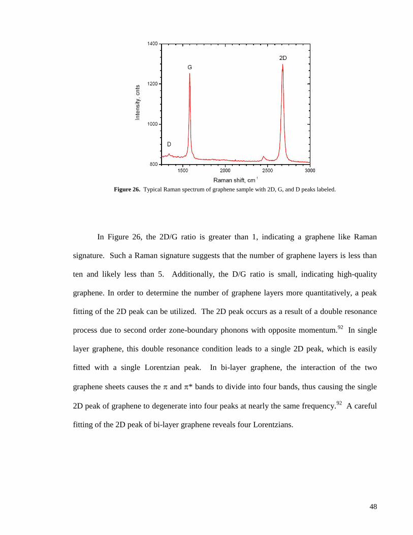
48
Figure 26. Typical Raman spectrum of graphene sample with 2D, G, and D peaks labeled.
In Figure 26, the 2D/G ratio is greater than 1, indicating a graphene like Raman
signature. Such a Raman signature suggests that the number of graphene layers is less than
ten and likely less than 5. Additionally, the D/G ratio is small, indicating high-quality
graphene. In order to determine the number of graphene layers more quantitatively, a peak
fitting of the 2D peak can be utilized. The 2D peak occurs as a result of a double resonance
process due to second order zone-boundary phonons with opposite momentum.92
In single
layer graphene, this double resonance condition leads to a single 2D peak, which is easily
fitted with a single Lorentzian peak. In bi-layer graphene, the interaction of the two
graphene sheets causes the and * bands to divide into four bands, thus causing the single
2D peak of graphene to degenerate into four peaks at nearly the same frequency.92
A careful
fitting of the 2D peak of bi-layer graphene reveals four Lorentzians.

49
2.2.5 – X-ray Photoelectron Spectroscopy
X-ray photoelectron spectroscopy (XPS) is a quantitative spectroscopic technique that
uses a beam of x-rays to analyze the surface chemistry and composition of the top 1 – 10 nm
of a sample. XPS utilizes a monochromatic beam of X-rays ranging from 1 to 2 keV to eject
photoelectrons from the core level electrons of atoms within the sample. The energy of the
ejected electrons is measured by a high-resolution spectrometer, from which the binding
energy of the electron within the atom is determined. Because the binding energy of an
electron is dependent on its chemical surroundings, XPS allows not only for determination of
elemental, but also chemical identification.
A Kratos Analytical Axis Ultra XPS system with a 15 m spatial resolution was used
to collect all XPS spectra in this work. The system uses a Al K-alpha x-ray source. XPS
spectra were utilized to determine the oxidation state of the as-deposited and post-processed
dielectrics and also to characterize the surface chemistry of the graphene during device
processing and patterning.
2.3 – Device and Test Structure Fabrication
In this work, various test structures and electronic devices were prepared on
graphitized SiC substrates using conventional device processing techniques. The first step in
this process was the careful cleaning of the graphitized samples. Next, the isolation level
was lithographically patterned across the sample. In this work, a GCA 8000 i-line stepper
was used to pattern the samples at all levels. With the isolation level patterned, a plasma etch
was employed to etch away the exposed graphene and isolate the active regions, after which
all photoresist was stripped from the sample and the sample was cleaned. The isolation level

50
was used to isolate the active regions of the devices and eliminate any shunt conductances.
As shown in figure 27, the patterning and deposition of the source/drain contacts followed,
with appropriate pre-process and/or post-process steps applied before or after the deposition
of the contacts.
Figure 27. Schematic representation of the various steps involved from in fabricating graphene devices starting with
graphene synthesis.
The contacts were deposited using e-beam evaporation, after which the sample was
again stripped and cleaned. Next, top-gate dielectrics were deposited over the entirety of the
sample, after which a pad-open was patterned and performed in order to remove the
dielectric covering the source/drain contact pads. Finally, patterning and deposition of the
top-gate contacts took place, after which the samples were ready for electrical
characterization following one last strip and clean. More details regarding device processing
are presented in the following sections.

51
2.3.1 – Sample Preparation and Cleaning
After graphitization and before device processing, graphene samples underwent an
initial standard clean that included soaking each sample in a PRS‐3000 (alfa aesar) bath
heated to 90°C for 30 minutes, followed by an isopropyl alcohol bath for 1 minute, and N2
blow dry. This standard clean was then utilized repeatedly throughout device processing to
simultaneously strip photoresist from the samples, clean them, and prepare them for
subsequent patterning and processing.
2.3.2 – Isolation
The first step in processing the samples was to define the active regions of the test
structures and devices. To accomplish this, first, a photoresist mask was prepared and
patterned across the sample. A bilayer resist stack consisting of LOR 5A (Microchem Corp.)
and Megaposit SPR-3012 (Rohm & Hass, Inc.) was used, where utilization of a bilayer resist
process allows for superior edge acuity compared to single layer resist stack. Although edge
acuity was not as much a concern for the isolation step as for the metal deposition step, the
use of a standard resist stack throughout all processing was preferred. The photoresist acted
as a protective mask that shielded the active regions from the isolation etch. The resist was
exposed using an i-line UV lightsource via the GCA 8000 stepper, after which the exposed
resist was developed in Microposit MF CD-26 developer (Rohm & Hass, Inc.). A DI water
bath and N2 blow dry followed the resist develop.
After developing the resist mask, the samples were exposed to an O2 plasma etch
using a PlasmaTherm PT720 Reactive Ion Etch tool. The O2 plasma etch lasts for 2 minutes
at 75 W and utilized a mixture of O2 and Ar gasses where 100 sccm of O2 and 8 sccm of Ar
were flowed into the etch chamber. The etch is effective in removing any exposed graphene
52
from the SiC substrate, where the resist mask is used to protect the active regions of the test
structures and devices. Finally, the samples were stripped and cleaned for the next step using
the standard clean as detailed in section 2.3.1.
2.3.3 – Source/Drain Contacts
The second step in processing the samples was to pattern and then deposit the first
layer of metallization (source/drain contacts) of the test structures and devices using a lift-off
process. To accomplish this, first, a photoresist mask was prepared and patterned across the
sample. A bilayer resist stack consisting of LOR 5A (Microchem Corp.) and Megaposit
SPR-3012 (Rohm & Hass, Inc.) was used, where utilization of a bilayer resist process allows
for superior edge acuity compared to single layer resist stack. The resist was exposed using
an i-line UV lightsource via the GCA 8000 stepper. The exposed resist was developed in
Microposit MF CD-26 developer (Rohm & Hass, Inc.). After developing the resist, a DI
water bath and N2 blow dry were used to remove any residual developer.
After developing the resist mask and before the metal deposition, a pre-deposition de-
scum was performed on certain samples in order to remove any resist residue from the
graphene surface. A Metroline M4L Plasma Etcher was used to perform the de-scum, which
could last 60 to 120 seconds at 100 W with 150 sccm of O2 and 50 sccm of He. The short
plasma etch was found to be an effective tool in reducing contact resistances.
After completing any pre-processing steps, the samples were loaded into the electron-
beam physical vapor deposition system (EBPVD), which was subsequently evacuated to <
10-6
Torr. In this work, a Semicore electron-gun/thermal evaporator was used to deposit the
source/drain metal stack, which consisted of two layers of metal. The first layer (10 nm)
could be one of several metals, including Cu, Ni, Ti, Pd, and Pt, while the second layer (50
53
nm) was always chosen to be gold. The deposition process was monitored using a quartz
crystal thickness monitor and metal deposition rate was controlled to a maximum of 0.3 nm
per second with an initial slow ramp in deposition rate. Additionally, a pre-soak was utilized
before deposition in order to create a uniform melt. Once the source/drain metals were
deposited, the samples were allowed to cool under vacuum before venting the deposition
chamber and removing the samples, after which the samples were stripped and cleaned for
the next step using the standard clean as detailed in section 2.3.1.
2.3.4 – Top-gate Dielectrics
The fourth step in device processing was to deposit the top-gate dielectric. This was
accomplished by depositing a thin layer of dielectric over the entirety of the sample, after
which a source/drain pad-open was performed. In this work, deposition of gate dielectric
was comprised of various steps, with ALD and EBPVD being utilized to prepare either
EBPVD seeded ALD films or EBPVD-only films.
EBPVD seeded ALD dielectrics utilized a ~2 – 3 nm seed layer of SiO2, Al2O3, or
HfO2 deposited via non-reactive EBPVD at < 1x10⁻⁶
Torr, using a Semicore electron-
gun/thermal evaporator. Following the organic clean, samples were loaded into an e‐beam
evaporation chamber and pumped to 1x10‐6 Torr, after which ~2 – 3 nm of the appropriate
oxide seed was deposited from a high purity oxide source. The deposition process was
monitored using a quartz crystal thickness monitor and deposition rate was controlled to a
maximum of 0.3 nm per second with an initial slow ramp in deposition rate. Additionally, a
pre-soak was utilized before deposition in order to create a uniform melt. The samples were
allowed to cool under vacuum before being removed from the deposition chamber. After
being removed from the e-beam chamber, samples were immediately loaded into the ALD

54
chamber to deposit the desired gate dielectric. The ALD chamber was preconditioned with 10
nm of the desired gate dielectric to reduce the introduction of any contaminants into the as-
deposited dielectrics. Atomic layer deposition was accomplished in two steps: seed
oxidation and dielectric deposition. First, seed oxidation was achieved using a 10 second
pulse of H2O followed by a 30 second wait, which was cycled 10 times at 100°C. This
oxidation step was utilized to insure that as-deposited EBPVD seeds were fully oxidized
before proceeding with deposition of the ALD dielectrics. Second, oxide deposition was
achieved utilizing a water based chemistry that required a pulse of water followed by a wait
period and a pulse of the correct precursor followed by another wait period. The necessary
pulses and wait periods were material and temperature specific, and happen according to a
set number of cycles. A Cambridge Savannah 200 atomic layer deposition tool was used to
deposit all ALD films in this work. Table 2 summarizes the seed material, ALD precursor,
and deposition temperatures utilized in this study.
Table 2. Summary of dielectric seed layer, precursor, and deposition temperature.
EBPVD seed material
ALD dielectric
material ALD precursor
deposition
temperature (C)
Al2O3 or HfO2 Al2O3 Triethylaluminum 300
Al2O3, HfO2, or SiO2 HfO2 Tetrakis(dimethylamino)hafnium 250
The seeded ALD process in this work can be considered similar to previous work
utilizing oxidized metal seeds (metalmetal-oxide),79,80
but with one important distinction:
the seed is deposited directly from a high-purity oxide source. This process, referred to as
oxide seeded ALD (O-ALD), omits the metal to metal-oxide phase transition of the oxidized
metal seeded process (M-ALD), which may be a source of transport degradation in graphene.
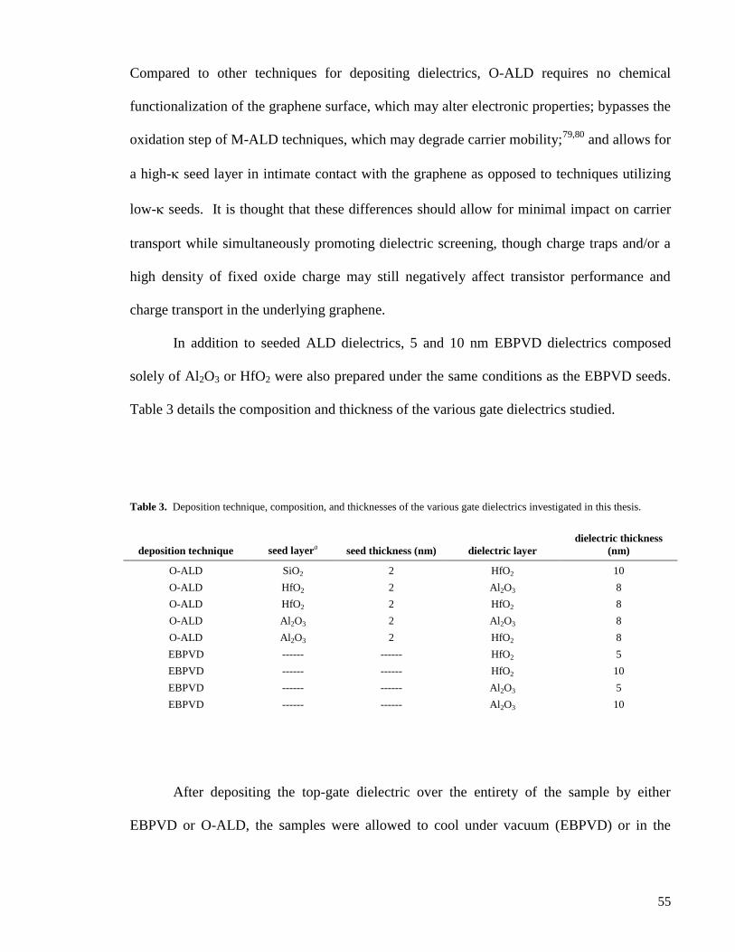
55
Compared to other techniques for depositing dielectrics, O-ALD requires no chemical
functionalization of the graphene surface, which may alter electronic properties; bypasses the
oxidation step of M-ALD techniques, which may degrade carrier mobility;79,80
and allows for
a high- seed layer in intimate contact with the graphene as opposed to techniques utilizing
low- seeds. It is thought that these differences should allow for minimal impact on carrier
transport while simultaneously promoting dielectric screening, though charge traps and/or a
high density of fixed oxide charge may still negatively affect transistor performance and
charge transport in the underlying graphene.
In addition to seeded ALD dielectrics, 5 and 10 nm EBPVD dielectrics composed
solely of Al2O3 or HfO2 were also prepared under the same conditions as the EBPVD seeds.
Table 3 details the composition and thickness of the various gate dielectrics studied.
Table 3. Deposition technique, composition, and thicknesses of the various gate dielectrics investigated in this thesis.
deposition technique seed layera seed thickness (nm) dielectric layer
dielectric thickness
(nm)
O-ALD SiO2 2 HfO2 10
O-ALD HfO2 2 Al2O3 8
O-ALD HfO2 2 HfO2 8
O-ALD Al2O3 2 Al2O3 8
O-ALD Al2O3 2 HfO2 8
EBPVD ------ ------ HfO2 5
EBPVD ------ ------ HfO2 10
EBPVD ------ ------ Al2O3 5
EBPVD ------ ------ Al2O3 10
After depositing the top-gate dielectric over the entirety of the sample by either
EBPVD or O-ALD, the samples were allowed to cool under vacuum (EBPVD) or in the
56
ALD system (O-ALD). After cooling to room-temperature, the samples were cleaned for the
next step using the standard clean as detailed in section 2.3.1.
2.3.5 – Pad-Open
The next step in device processing was the removal of the deposited gate dielectric
from the already deposited source/drain contact pads. Because the gate dielectric was
deposited over the entirety of the sample, this step was critical in exposing the contact pads
so that probes could make contact to the test structures and devices without the top gate
dielectric acting as a dielectric barrier. This step is accomplished using a photoresist mask to
protect the gate dielectric except in regions where probes need to make contact to the first
metallization layer, namely the source/drain contact pads. A bilayer resist stack consisting of
LOR 5A (Microchem Corp.) and Megaposit SPR-3012 (Rohm & Hass, Inc.) was used. The
resist was exposed using an i-line UV lightsource via the GCA 8000 stepper. The exposed
resist was developed in Microposit MF CD-26 developer (Rohm & Hass, Inc.). After
developing the resist, a DI water bath and N2 blow dry were used to remove any residual
developer.
After developing the resist mask, the samples were exposed to a reactive ion plasma
etch using an Applied Materials Magnetically Enhanced Reactive Ion Etch (MERIE)
dielectric etch tool. The MERIE etch lasts for 6 minutes at 70 W and utilized a mixture of
CHF3 and CF4 gasses. The etch is effective in removing the deposited top-gate dielectric
from the source/drain contact pads, where the resist mask is used to protect the dielectric in
other regions of the sample. Finally, the samples were stripped and cleaned for the next step
using the standard clean as detailed in section 2.3.1.

57
2.3.6 – Gate Contacts
The final step of device processing was the patterning and deposition of the top-gate
metal contact and contact pad. To accomplish this, first, a photoresist mask was prepared
and patterned across the sample. A bilayer resist stack consisting of LOR 5A (Microchem
Corp.) and Megaposit SPR-3012 (Rohm & Hass, Inc.) was used. The resist was exposed
using an i-line UV lightsource via the GCA 8000 stepper. The exposed resist was developed
in Microposit MF CD-26 developer (Rohm & Hass, Inc.). After developing the resist, a DI
water bath and N2 blow dry were used to remove any residual developer.
After developing the resist mask and before the metal deposition, a pre-deposition de-
scum was performed to remove any resist residue from the top-gate dielectric. A Metroline
M4L Plasma Etcher was used to perform the de-scum, which lasted 60 seconds at 100 W
with 150 sccm of O2 and 50 sccm of He.
After completing the plasma de-scum, the samples were loaded into the electron-
beam physical vapor deposition system (EBPVD), which was subsequently evacuated to <
10-6
Torr. In this work, a Semicore electron-gun/thermal evaporator was used to deposit the
gate metal stack, which consisted of a thin adhesion layer (10 nm) of Ti and a thick (50 nm)
Au overlayer. The deposition process was monitored using a quartz crystal thickness
monitor and metal deposition rate was controlled to a maximum of 0.3 nm per second with
an initial slow ramp in deposition rate. Additionally, a pre-soak was utilized before
deposition in order to create a uniform melt. Once the source/drain metals were deposited,
the samples were allowed to cool under vacuum before venting the deposition chamber and
removing the samples, after which the samples were stripped and cleaned for the next step
using the standard clean as detailed in section 2.3.1.

58
2.3.7 – Device Geometries
In this work, several different test structures and devices were fabricated. Transfer
length measurement (TLM) structures were used to evaluate the metal-graphene contacts,
and consisted of a set of six pairs of metal pads with varying distance between each pair of
pads (Figure 28). The width of the pads, Z, was 25 m and consistent between all sets, while
pad spacing varied for each pair of pads and ranged from 0.75 m to 3.0 m.
Figure 28. Optical micrograph of TLM test structures (0.7 refers to a pad spacing, d, of 0.75 m.
Van der Pauw (VdP) structures were used to measure Hall mobility and carrier
concentration and consisted of 5x5 m squares as shown in Figure 29. Both gated and un-
gated VdP structures were prepared.
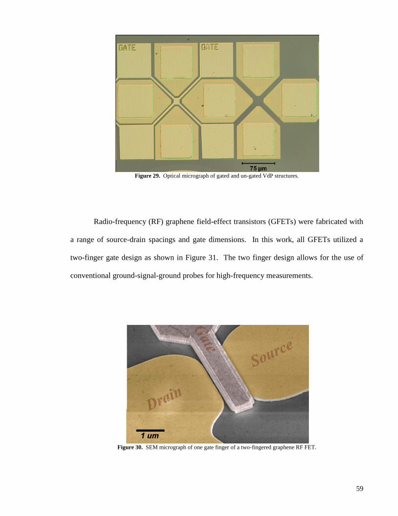
59
Figure 29. Optical micrograph of gated and un-gated VdP structures.
Radio-frequency (RF) graphene field-effect transistors (GFETs) were fabricated with
a range of source-drain spacings and gate dimensions. In this work, all GFETs utilized a
two-finger gate design as shown in Figure 31. The two finger design allows for the use of
conventional ground-signal-ground probes for high-frequency measurements.
Figure 30. SEM micrograph of one gate finger of a two-fingered graphene RF FET.

60
Figure 31. Cross sectional schematic of graphene RF FET utilizing a EBPVD seeded ALD top-gate dielectric.
Transistors utilized source-drain spacings of either 1.0 or 1.5 m, with most device
testing performed on the GFETs utilizing a source-drain spacing of 1.0 m. On each die,
GFETs of varying gate length (Lg) and gate width (Wg) were patterned. Gate widths were
either 3, 5, 10, or 25 m, while gate lengths were either 1.0, 1.25, or 1.5 m.
2.4 – Electrical Characterization
2.4.1 – Contact Resistance
In order to characterize both contact resistance and specific contact resistance, the
transfer length method (TLM) was utilized. The TLM method utilized the TLM structures
described in section 2.3.7. The technique required an additional etch to restrict the current
flow to the graphene that exists between the two pads and eliminate any shunt conductances.
This etch was accomplished during the isolation step. In this technique, direct current (DC)
measurements of the total resistance (RT) between two contact metallizations were plotted as
a function of the spacing between the contacts. Plotting RT in this way allowed for the
extraction of contact resistance (RC), sheet resistance (RS), and transfer length (LT), where RT
was the sum of the metal resistance (RM), the metal/graphene interfacial resistance (RC), and
the graphene sheet resistance (RS) as shown in Figure 32.
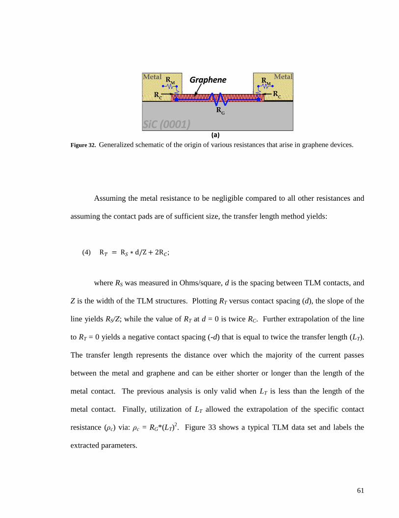
61
Figure 32. Generalized schematic of the origin of various resistances that arise in graphene devices.
Assuming the metal resistance to be negligible compared to all other resistances and
assuming the contact pads are of sufficient size, the transfer length method yields:
(4) ;
where RS was measured in Ohms/square, d is the spacing between TLM contacts, and
Z is the width of the TLM structures. Plotting RT versus contact spacing (d), the slope of the
line yields RS/Z; while the value of RT at d = 0 is twice RC. Further extrapolation of the line
to RT = 0 yields a negative contact spacing (-d) that is equal to twice the transfer length (LT).
The transfer length represents the distance over which the majority of the current passes
between the metal and graphene and can be either shorter or longer than the length of the
metal contact. The previous analysis is only valid when LT is less than the length of the
metal contact. Finally, utilization of LT allowed the extrapolation of the specific contact
resistance (ρc) via: ρc = RG*(LT)2. Figure 33 shows a typical TLM data set and labels the
extracted parameters.
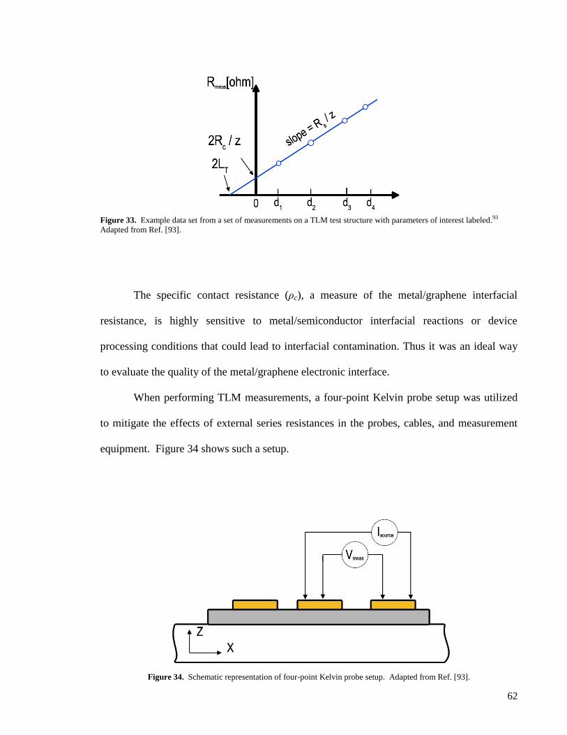
62
Figure 33. Example data set from a set of measurements on a TLM test structure with parameters of interest labeled.93
Adapted from Ref. [93].
The specific contact resistance (ρc), a measure of the metal/graphene interfacial
resistance, is highly sensitive to metal/semiconductor interfacial reactions or device
processing conditions that could lead to interfacial contamination. Thus it was an ideal way
to evaluate the quality of the metal/graphene electronic interface.
When performing TLM measurements, a four-point Kelvin probe setup was utilized
to mitigate the effects of external series resistances in the probes, cables, and measurement
equipment. Figure 34 shows such a setup.
Figure 34. Schematic representation of four-point Kelvin probe setup. Adapted from Ref. [93].

63
Employing a four-point technique, two probes are utilized to carry the current while
the other two are utilized to measure the voltage between the contact pads. This setup allows
the voltage measuring probes to carry effectively zero current. Thus, the probe and cable
resistances can be eliminated by calculating resistance using the voltage measured between
the two voltage measuring probes and the current carried by the current carrying probes.
2.4.2 – Hall Effect Measurements
Hall effect measurements were used to evaluate the effect of seed layer and dielectric
overlayer on carrier transport within the graphene by measuring carrier density and Hall
mobility before and after deposition of the dielectric overlayer. Changes in carrier density
were indicative of a charge transfer process between the graphene and dielectric, as discussed
in section 1.3.2., while changes in Hall mobility might be linked to an increase in scattering
due to impurities or a decrease in scattering due to dielectric screening.
The Hall effect measurement relies on the Hall effect to determine carrier density.
The Hall effect is the effect produced when a perpendicular magnetic field (B) is applied to a
current. The applied magnetic field induces a Lorentz force on the charge carriers according
to:
(5) ;
where the Lorentz force, F, on each carrier is a function of the carrier charge, q, the
carrier velocity, v, and the applied magnetic field, B. The Lorentz force in conjunction with
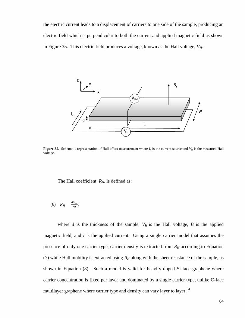
64
the electric current leads to a displacement of carriers to one side of the sample, producing an
electric field which is perpendicular to both the current and applied magnetic field as shown
in Figure 35. This electric field produces a voltage, known as the Hall voltage, VH.
Figure 35. Schematic representation of Hall effect measurement where Ix is the current source and VH is the measured Hall
voltage.
The Hall coefficient, RH, is defined as:
(6)
;
where d is the thickness of the sample, VH is the Hall voltage, B is the applied
magnetic field, and I is the applied current. Using a single carrier model that assumes the
presence of only one carrier type, carrier density is extracted from RH according to Equation
(7) while Hall mobility is extracted using RH along with the sheet resistance of the sample, as
shown in Equation (8). Such a model is valid for heavily doped Si-face graphene where
carrier concentration is fixed per layer and dominated by a single carrier type, unlike C-face
multilayer graphene where carrier type and density can vary layer to layer.94
65
(7)
(8)
where Nsh is the sheet carrier density of charge carriers in carriers/cm2, Hall is the
Hall mobility in cm2/Vsec, and Rsh is sheet resistance in Ohms/square. Hall mobility is a
measure of carrier mobility that is determined from the Hall effect and differs from
conductivity mobility by the Hall factor, r. The Hall factor usually lies between 1 and 2 and
is related to the type of scattering mechanisms present in the sample. For the case of ideal
charged impurity scattering, which is thought to play a dominant role in graphene samples, r
is typically 1.93.95,96
The Hall effect measurements were carried out using the Van der Pauw (VdP)
structures as described in section 2.3.7. Hall effect measurements were made under high
vacuum (< 5x10⁻⁸
Torr) at 300 K in a ±0.5 T magnetic field prior to and following deposition
of the gate dielectric using a 10 A direct current source. Hall effect measurements allowed
direct sampling of carrier density and Hall mobility without relying on curve fitting. It also
had the advantage of removing any uncertainty due to the accurate measurement of back or
top gate capacitances, which is important for the case of top-gated graphene.97
Samples were
annealed in situ and under vacuum at 400 K for 60 min before measurement in order to
ensure desorption of water or other contaminants from the surface of the graphene,
preventing any extrinsic doping of the EG except that caused by the gate dielectric or the
substrate. Gated Hall effect measurements were also performed under vacuum to determine
the extent to which carrier density could be modulated by gate bias. In addition to Hall effect
measurements under vacuum, both un-gated and gated Hall effect measurements in ambient
atmosphere were also performed.
66
Hall effect measurements under vacuum were preformed in a LakeShore CPX-VF
Cryogenic Probe Station. The system utilizes a refrigerant coolant system to cool a
superconducting magnet to 5 K, allowing for magnetic fields up to 2.5 T in a vertical field
arrangement. Additionally, temperature controllers allowed for measurements from 2 – 400
K, while a Varian turbo pump was utilized to evacuate the system before cooling. For Hall
effect measurements under ambient conditions, a Nanometrics Hall System was used. The
Nanometrics system employs a 0.5 T permanent magnet in a vertical field arrangement which
can be mechanically rotated into positive and negative field orientations. Hall effect
measurements under positive and negative fields were averaged together in an attempt to
account for any non-symmetric effects as a function of geometry. Both systems sourced a 10
A direct current to measure sheet resistance and Hall voltages using a Van der Pauw Hall
arrangement.
2.4.3 – Direct Current Electrical Characterization of Transistors
GFET performance was characterized using drain current versus gate voltage (Ids-Vgs)
sweeps at Vds=1V, also referred to as a transfer curve, and drain current versus drain voltage
(Ids-Vds) sweeps at select gate biases. Typical Ids-Vgs plots for samples utilizing the ~10 nm
thick top-gate dielectrics were swept from -3 V < Vgs < 3 V, although voltage range scaled
with dielectric thickness. From these plots, several parameters of interest were extracted,
listed in Table 4.

67
Table 4. Parameters of interest extracted from direct current measurements of GFETs.
parameter definition
Ids,max Peak drive current during a single Ids-Vgs sweep.
Ids,min Minimum drive current during a single Ids-Vgs sweep.
On-off Ratio Ratio of peak drive current to minimum drive current, Ids,max / Ids,min .
gm,max Peak transconductance (gm), where
.
gm,min Minimum transconductance (gm), where
.
Vhalf,forward Voltage where
as Vgs is swept from negative to positive bias.
Vhalf,reverse Voltage where
as Vgs is swept from positive to negative bias.
Vhalf Hysteresis between Ids-Vgs sweeps, Vhalf,forward - Vhalf,reverse
Ig,leak Maximum gate leakage current during a single Ids-Vgs sweep.
Peak drive current (Ids,max), peak transconductance (gm,max), an on-off ratio were
extracted from the Ids-Vgs sweeps. Additionally, maximum gate leakage current (Ig,leak) and
minimum drive current (Ids,min) where extracted from the plots. Finally, hysteresis was
calculated from the Ids-Vgs sweeps and was defined as the difference between Vhalf,forward and
Vhalf,reverse, where Vhalf,forward was the voltage at which the current was halfway between Ids,min
and Ids,max while sweeping from negative to positive gate biases and Vhalf,reverse was the same
voltage while sweeping from positive to negative gate biases. Figure 36 shows a typical
transfer curve. These parameters were important in comparing the various gate dielectrics
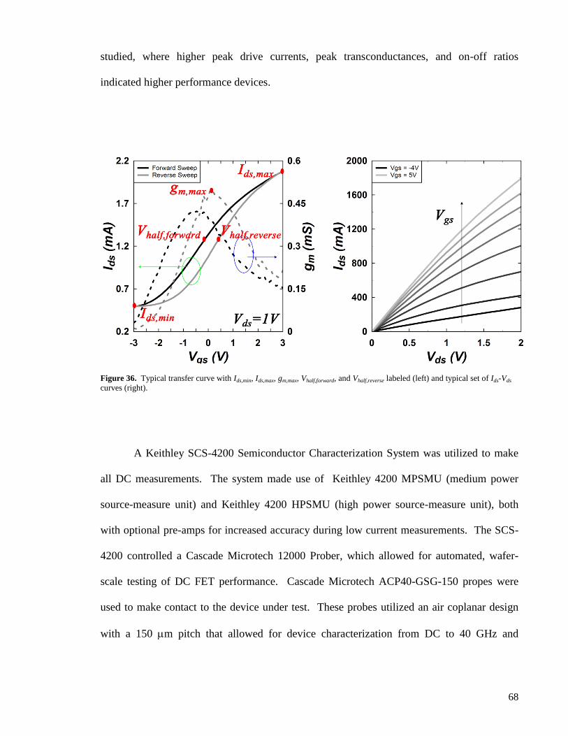
68
studied, where higher peak drive currents, peak transconductances, and on-off ratios
indicated higher performance devices.
Figure 36. Typical transfer curve with Ids,min, Ids,max, gm,max, Vhalf,forward, and Vhalf,reverse labeled (left) and typical set of Ids-Vds
curves (right).
A Keithley SCS-4200 Semiconductor Characterization System was utilized to make
all DC measurements. The system made use of Keithley 4200 MPSMU (medium power
source-measure unit) and Keithley 4200 HPSMU (high power source-measure unit), both
with optional pre-amps for increased accuracy during low current measurements. The SCS-
4200 controlled a Cascade Microtech 12000 Prober, which allowed for automated, wafer-
scale testing of DC FET performance. Cascade Microtech ACP40-GSG-150 propes were
used to make contact to the device under test. These probes utilized an air coplanar design
with a 150 m pitch that allowed for device characterization from DC to 40 GHz and
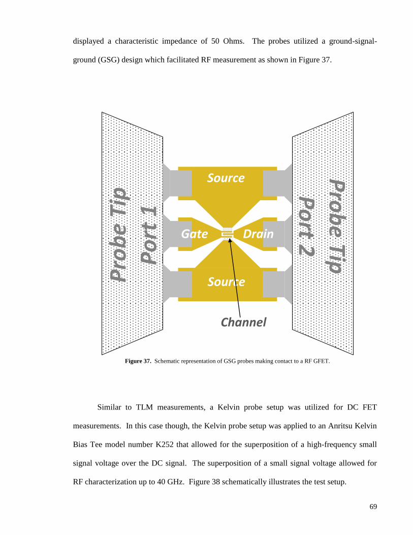
69
displayed a characteristic impedance of 50 Ohms. The probes utilized a ground-signal-
ground (GSG) design which facilitated RF measurement as shown in Figure 37.
Similar to TLM measurements, a Kelvin probe setup was utilized for DC FET
measurements. In this case though, the Kelvin probe setup was applied to an Anritsu Kelvin
Bias Tee model number K252 that allowed for the superposition of a high-frequency small
signal voltage over the DC signal. The superposition of a small signal voltage allowed for
RF characterization up to 40 GHz. Figure 38 schematically illustrates the test setup.
Source
Source Pro
be
Tip
Po
rt 1
Pro
be Tip
Po
rt 2
Gate Drain
Figure 37. Schematic representation of GSG probes making contact to a RF GFET.
Channel

70
2.4.4 – Small Signal Characterization of Transistors
Small signal transistor characterization was completed using an Anritsu 37269B
Vector Network Analyzer which was integrated with the Keithley SCS-4200 characterization
system as shown in Figure 38. The use of a vector network analyzer allows for the accurate
characterization of scattering parameters (S-parameters) by measuring the amplitude and
phase of test signals going into and out of the device under test (DUT). The Anritsu network
Figure 38. Schematic representation of the test setup used for DC and RF FET characterization showing the connections
between the SCS-4200, Anritsu VNA, and device under test.
HPSMU
MPSMU
SCS-4200
Force
Force
Sense
Sense
K252 Bias Tee
K252 Bias Tee
DUT
Anritsu VNA
Port 1 Port 2

71
analyzer was utilized to measure S-parameters from 50 MHz to 40 GHz at select bias
conditions.
A short-open-load-through (SOLT) calibration was performed before all RF
measurement sessions using a Suss MicroTec CSR-8 Calibration Substrate. This allowed for
the quantification of systematic errors in the setup by moving the plane of measurement to
the probe tips and calibrating out any error due to cabling or probes. The SOLT method is a
two-port calibration which is typical for coaxial transmissions. It relies on a short, open, and
load at each port in order to measure reflection errors and isolation between the ports.
Additionally, the through standard is used to measure frequency response tracking. After
calibration, the device measurements can be error-corrected for greater accuracy.
Extrinsic small signal current gain (
, where I2 is the ouput current and I1 is
the input current) was extracted from the devices in order to determine the extrinsic current
gain cut-off frequency (fT) of the transistors, where H21 is determined from the measured S-
parameters according to Equation (9).
(9)
Additionally, on-wafer de-embed structures consisting of open and short structures
were used to calibrate out pad and device parasitics so that intrinsic small signal current gain
might be characterized. The de-embed process follows Equation (10), where the measured
S-parameters of the open and short structures are removed from the S-parameters of the DUT
by first converting the S-parameters to Y-parameters.
(10)
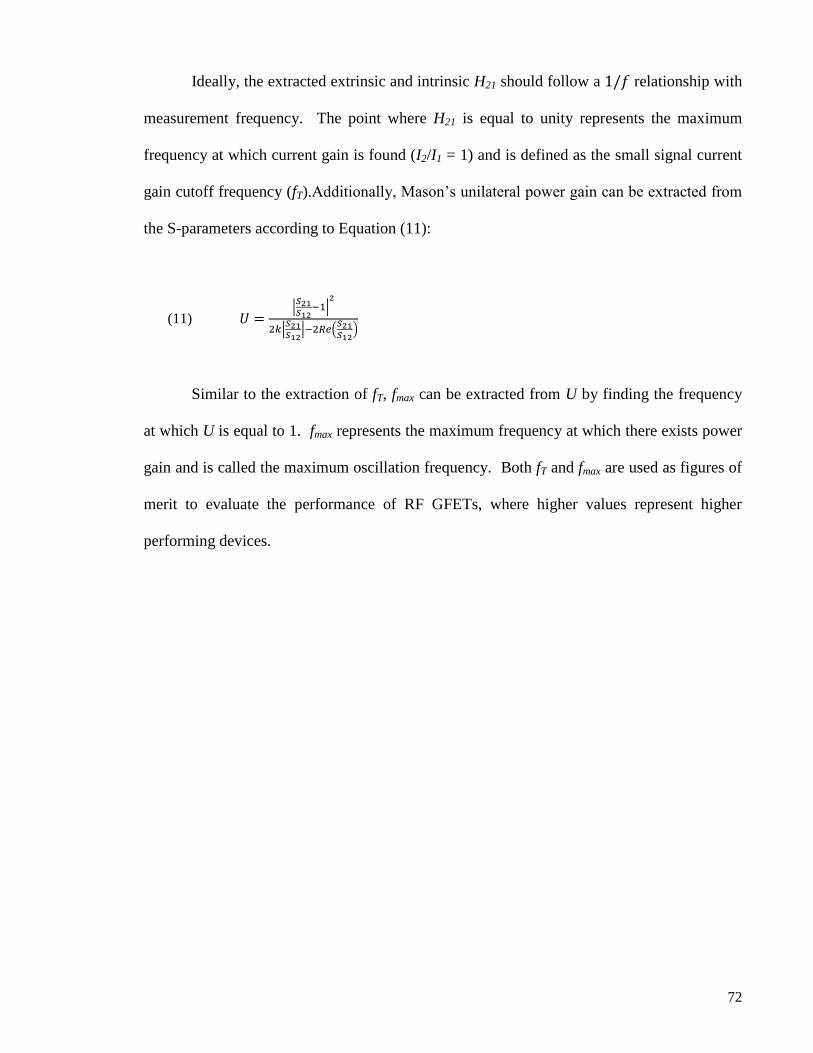
72
Ideally, the extracted extrinsic and intrinsic H21 should follow a relationship with
measurement frequency. The point where H21 is equal to unity represents the maximum
frequency at which current gain is found (I2/I1 = 1) and is defined as the small signal current
gain cutoff frequency (fT).Additionally, Mason’s unilateral power gain can be extracted from
the S-parameters according to Equation (11):
(11)
Similar to the extraction of fT, fmax can be extracted from U by finding the frequency
at which U is equal to 1. fmax represents the maximum frequency at which there exists power
gain and is called the maximum oscillation frequency. Both fT and fmax are used as figures of
merit to evaluate the performance of RF GFETs, where higher values represent higher
performing devices.
73
Chapter Three: Results
3.1 – Optimizing the Metal-Graphene Interface
As discussed in Section 1, the metal-graphene interface is a critical component of the
graphene transistor that has the potential to limit ultimate device performance in the form of
parasitic resistances. These parasitic resistances become even more important as the channel
is scaled to shorter lengths due to the fact that the channel resistance, Rch, scales with channel
length while contact resistances, RC, does not. Although the metal-graphene interface is not
well understood, it is clear from initial work that the metal-graphene interface must be
improved.
Initial work studying the effect of various gate dielectrics on GFET performance
indicated that the metal-graphene interface was of poor quality when metal contacts were
simply evaporated onto the graphene without any pre- or post-processing. Figure 39 shows
two subsequent transfer curves for one of these initial devices. The device utilized a Ti/Au
metal stack for source/drain contact metallizations and employed no pre- or post-processing.
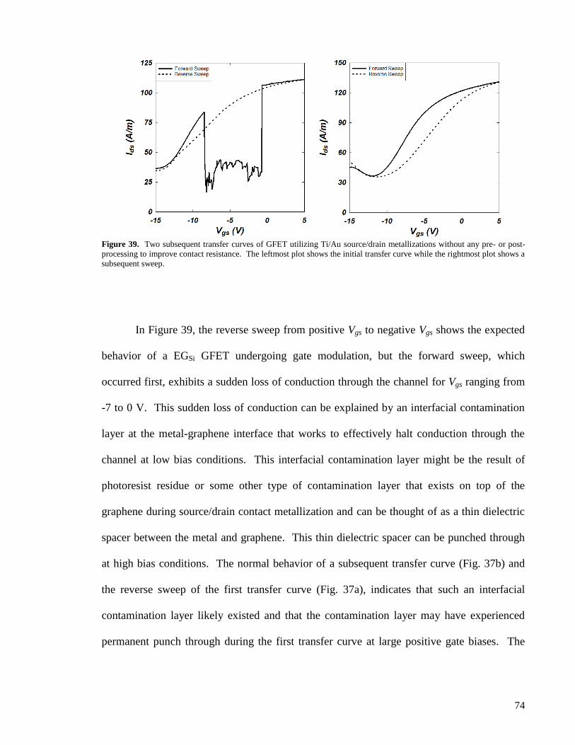
74
Figure 39. Two subsequent transfer curves of GFET utilizing Ti/Au source/drain metallizations without any pre- or post-
processing to improve contact resistance. The leftmost plot shows the initial transfer curve while the rightmost plot shows a
subsequent sweep.
In Figure 39, the reverse sweep from positive Vgs to negative Vgs shows the expected
behavior of a EGSi GFET undergoing gate modulation, but the forward sweep, which
occurred first, exhibits a sudden loss of conduction through the channel for Vgs ranging from
-7 to 0 V. This sudden loss of conduction can be explained by an interfacial contamination
layer at the metal-graphene interface that works to effectively halt conduction through the
channel at low bias conditions. This interfacial contamination layer might be the result of
photoresist residue or some other type of contamination layer that exists on top of the
graphene during source/drain contact metallization and can be thought of as a thin dielectric
spacer between the metal and graphene. This thin dielectric spacer can be punched through
at high bias conditions. The normal behavior of a subsequent transfer curve (Fig. 37b) and
the reverse sweep of the first transfer curve (Fig. 37a), indicates that such an interfacial
contamination layer likely existed and that the contamination layer may have experienced
permanent punch through during the first transfer curve at large positive gate biases. The

75
existence of a thin contamination layer also might explain the interesting results of substrate
modulated contact resistance in double-gated graphene FETs.98
,99
In order to determine the presence of any contamination on the surface of the
graphene, X-ray photo-electron spectroscopy (XPS) was utilized on a pristine EGSi surface
and compared to EGSi that has been initially coated with photoresist (either Microchem LOR
5A or SPR-3012), subsequently flood exposed to ultraviolet light, and finally soaked in resist
developer. Figure 40 compares the XPS spectra of these three graphene samples.
Figure 40. X-ray photoelectron spectroscopy reveals that the graphene and SiC peaks are severely attenuated following
lithographic processing, suggesting that residual resist residue remains. Adapted from Ref. [100].
The XPS results showed that the use of photoresist in graphene processing leads to
the appearance of both C-O and C=O peaks in the XPS spectra (Fig. 40), while pristine EGSi
76
showed no such peaks.100
These peaks indicated high levels of carbon-oxygen single (C-O)
and double (C=O) bonds and was indicative of a residual contamination layer as a result of
photolithographic processing. Additionally, Figure 40 showed a severe attenuation in the
graphene and SiC XPS peaks after photolithographic processing, indicative of a
contamination layer that coated the EGSi samples.
Although pristine graphene exhibited no contamination, the necessity to pattern the
graphene during the isolation step and before source/drain metallization to ensure good
adhesion of the source/drain contacts prompted the investigation into pre- and post-process
steps that could effectively remove the residual photoresist contamination from the graphene.
3.1.1 – Effect of Pre- and Post-Processing on Metal-Graphene Interface
Previous work suggested that thermal treatments in an H2 ambient at elevated
temperature (> 400 C) provided a route to effectively remove photoresist residue following
photolithographic processing;101
as a result, initial attempts utilized a rapid thermal heat
treatment to contact graphene “through” the resist residue. Whereas previous work showed
reduced photoresist residue after thermal treatments for uncovered graphene samples, the
remaining residue for the metalized graphene suggested that an “in situ” processing step
could lead to significantly reduced contamination compared to the post-metallization thermal
treatment. This was due to the fact that contact metallization likely reduces or prevents the
photoresist contamination from being effectively reduced (removed) by the post-process H2
heat treatment.
The utilization of oxygen plasma is often used to isolate the graphene channel in
devices by etching away the graphene; however, we found it can also be utilized to remove
residual resist prior to metal deposition when implemented properly. Figure 41 shows the

77
effect of O2 plasmas of various durations on the XPS (left) and Raman spectra (right) of EGSi
samples that had undergone photolithographic processing using SPR-3012 photoresist.
Figure 41. As evidenced by the reduction in SiC substrate attenuation, resist residue is successfully removed through the
utilization of an O2 plasma treatment (a), however, as the plasma treatment progresses, the underlying graphene degrades.
Raman spectroscopy (b) confirms the formation of a high density of defects (evidenced by the increase in D peak intensity),
which correlates with the formation of C-O bonds found in XPS (a). Adapted from Ref. [Error! Bookmark not defined.].
In Figure 41, the use of an oxygen plasma after photolithographic processing was
shown to reduce the attenuation of the SiC substrate XPS peak, yet also to introduce a
significant C-O peak. The reduction in attenuation of the SiC peak was attributed to the
removal of resist residue through the utilization of an O2 plasma treatment; however, as the
plasma treatment progresses, it is thought that the O2 plasma introduced a significant number
of defects into the exposed graphene. Raman spectroscopy (Fig. 41, right) was utilized to
confirm the formation of a high density of defects (evidenced by the increase in D peak
intensity), which correlated with the formation of C-O bonds found in XPS.

78
Although XPS results indicated the successful removal of residual photoresist
contamination through use of an O2 plasma, the increase in defectiveness of the exposed
graphene suggested that the metal-graphene interface might be degraded. TLM structures
were utilized to determine the absolute effect of pre- and post-treatments on the specific
contact resistivity, ρc, of the metal-graphene interface, shown in Figure 42.
The use of a lithographic process without surface modification or rapid thermal heat
treatment (400C, 60 – 240 sec, post-metallization) generally resulted in ρc values > 10-5
Ohm-cm2 (Figure 42), indicating a poor interface between the graphene and metal. The high
ρc was attributed to remaining photoresist contamination on the surface of the graphene prior
to contact metallization.
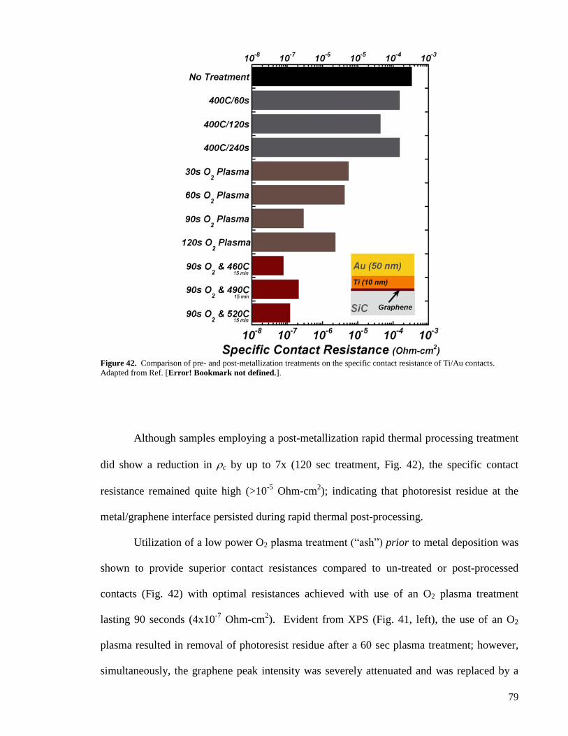
79
Figure 42. Comparison of pre- and post-metallization treatments on the specific contact resistance of Ti/Au contacts.
Adapted from Ref. [Error! Bookmark not defined.].
Although samples employing a post-metallization rapid thermal processing treatment
did show a reduction in c by up to 7x (120 sec treatment, Fig. 42), the specific contact
resistance remained quite high (>10-5
Ohm-cm2); indicating that photoresist residue at the
metal/graphene interface persisted during rapid thermal post-processing.
Utilization of a low power O2 plasma treatment (“ash”) prior to metal deposition was
shown to provide superior contact resistances compared to un-treated or post-processed
contacts (Fig. 42) with optimal resistances achieved with use of an O2 plasma treatment
lasting 90 seconds (4x10⁻⁷
Ohm-cm2). Evident from XPS (Fig. 41, left), the use of an O2
plasma resulted in removal of photoresist residue after a 60 sec plasma treatment; however,
simultaneously, the graphene peak intensity was severely attenuated and was replaced by a
80
combination of C-C and C-O bonds. Expectedly, as the etch time was increased to 120 sec
the C-C bonding was further reduced, being replaced by C-O bonds.
Degradation of the graphene exposed to the O2 plasma was confirmed by Raman
spectroscopy (Fig. 41, right), where the D/G peak ratio indicated a graphene domain size of
~10 nm.102
Even under the most benign conditions there was degradation in the structure of
the graphene (evidenced by the increase in D/G ratio); however, ρc continued to improve as
the O2 plasma treatment time increased from 30 – 90 sec to an average value of 4x10⁻⁷
Ohm-
cm2. Upon reaching 120 sec, ρc began increasing again, which was correlated with a severe
degradation in the Raman 2D peak intensity (Fig. 41, right), suggesting that the bulk of the
sp2-bonding expected in graphene had been destroyed. Additionally, an increased fraction of
the chemistry included C-O bonding (Fig. 41, left), suggesting that the formation of
graphene-oxide might have occurred.
Initial evaluation of the “defectiveness” measured by Raman spectroscopy may lead
to the conclusion that the graphene is no longer suitable for device applications; however,
only the graphene that will be covered by the metal contact is exposed to the O2 plasma and
one should consider that, in all cases, the graphene channel is protected. Post-contact
metallization Hall effect measurements indicated that graphene between the contacts
remained unaffected by the plasma treatment, experiencing no degradation in carrier mobility
compared to graphene test structures utilizing un-treated contacts (utilizing no pre- or post-
processing) or utilizing contacts prepared using a post-metallization thermal treatment with
H2.

81
3.1.2 – Effect of Combining Pre- and Post-Processing on Metal-Graphene Interface
For an additional set of EGSi samples, pre-process O2 plasma treatments were
combined with post-process thermal treatments at various temperatures. Thermal treatments
with H2 were performed after removal of photoresist residue by low power O2 plasma etch
and contact metallization. Thermal treatments were increased in duration to 15 minutes.
Following heat treatment, there was a 1.3 – 5x reduction in specific contact resistance
compared to the O2 plasma treatment alone, as shown in Figure 42. An optimized specific
contact resistance of approximately 5x10⁻⁸
Ohm-cm2 was achieved by combining an O2
plasma pre-treatment with a thermal treatment at 450 – 475 C.
3.2 – Effect of Choice of Metal on the Metal-Graphene Interface
As discussed in Section 1, theory suggests that the use of contact metallization with a
large difference in work function (φ) compared to graphene may result in a charge transfer
that leads to doping of the underlying graphene and formation of a dipole at the metal-
graphene interface. The charge transfer process leads to an increased density of states in the
graphene at the metal-graphene interface and should reduce contact resistance at the metal-
graphene interface. To explore this, metal contacts were prepared using a 90 sec O2 plasma
etch pre-treatment prior to deposition of Al (φ = 4.31), Ti (φ = 4.35), Cu (φ = 4.7), Pd (φ =
5.16), Ni (φ = 5.23), or Pt (φ = 5.64) metals.103
Graphene exhibits an electron work function
of 4.49 eV, resulting in absolute work function differences ranging from -0.2 to 1.2eV,
although effective differences may be different due to impurities or the presence of defects at
the metal-graphene interface. Such defects might lead to a dramatic change in the difference
between the two material’s work functions by altering the graphene metal spacing and the

82
dipole interaction at the metal-graphene interface.41,60,65
Figure 43 shows the resulting
average specific contact resistances measured from fifteen TLM structures and plots them as
a function of the theoretical ideal work function difference between the metal (first layer) and
graphene.
Figure 43. Comparison of specific contact resistance for different composition contact metallizations (using a O2 plasma
pre-treatment). Adapted from Ref. [Error! Bookmark not defined.].
Although φ varied from -0.2 to 1.2eV, little difference in specific contact resistance
between metallizations was found. While there was a clear lack of trend with φ, it is
important to note that the graphene in this work was fundamentally altered through use of O2
plasma pre-treatment and can no longer be considered “pristine” at the metal-graphene
interface. XPS and Raman spectroscopy (Fig. 41) indicated that the graphene was highly
defective with a large fraction (> 10%) of C-O bonds. The highly defective nature of the

83
graphene and chemical modification at the metal-graphene interface could explain the
relatively similar specific contact resistances between metallizations, where process
dependent chemisorptions/physisorption differences may lead to a change in the effective
work function difference at the metal-graphene interface.66
Finally, it is important to note that the use of some metallizations, even with
acceptable specific contact resistance, may not be warranted due to loss of adhesion or highly
non-uniform surface coverage. Specific examples of common issues related to the deposition
of aluminum and copper on graphene surfaces are illustrated in Figures 44 and 45.
Figure 44. SEM micrograph of Al/Au contact metallization showing significant delamination. Adapted from Ref. [Error!
ookmark not defined.].
Figure 44 is an SEM micrograph that shows that the use of aluminum as a first level
metallization resulted in severe delamination of the contacts from the graphene surface. The
inability of the Al/Au contact metallization to provide sufficient contact to the underlying
graphene was evidenced by TLM measurements which revealed exceedingly high and

84
variable specific contact resistances. This phenomenon was also found to occur in
metallization schemes that utilized layers of Pd or Pt with thicknesses greater than 15 nm,
although use of Pd or Pt layers <15 nm resulted in no delamination.
Figure 45. . AFM micrograph of thin Cu films deposited on graphene showing agglomeration of Cu to the extent that it was
not useful in device processing. Adapted from Ref. [Error! Bookmark not defined.].
Figure 45 is an atomic force micrograph of a 5 nm Cu film deposited on graphene that
shows an island-like growth morphology for Cu on graphene. Islands exhibited heights as
high as 20 nm, suggesting that the utilization of copper as a first layer resulted in highly non-
uniform metallization. Such a morphology is unacceptable for device processing, as
evidenced by the unacceptably high specific contact resistances listed in Figure 43.
3.3 – Depositing Gate Dielectrics on Graphene
As discussed in Section 1, the dielectric-graphene interface is a critical component of
the graphene transistor that has the potential to limit ultimate device performance in the form
of degraded transport properties. In this thesis, a novel technique for the deposition of
dielectrics on graphene by atomic layer deposition (ALD) was investigated. This technique

85
utilized direct deposited oxide films as a seed layer for subsequent growth of ALD dielectric
overlayers, referred to as O-ALD. This technique differed from previous work which
utilized thin metal seeds that were oxidized to form a seed layer for subsequent ALD,
referred to as M-ALD, and previous work which utilized low- polymer seeds for subsequent
ALD.
Compared to other techniques for depositing dielectrics, O-ALD requires no chemical
functionalization of the graphene surface, which may alter electronic properties; bypasses the
oxidation step of M-ALD techniques, which may degrade carrier mobility;79,80
and allows for
a high- seed layer in intimate contact with the graphene as opposed to techniques utilizing
low- seeds. It is thought that these differences should allow for minimal impact on carrier
transport while simultaneously promoting dielectric screening, though charge traps and/or a
high density of fixed oxide charge may still negatively affect transistor performance and
charge transport in the underlying graphene.
3.3.1 – Dielectric Film Morphology
Similar to previous work utilizing oxidized metal seeds,80
seeding by direct deposited
oxide was found to be an effective technique for the nucleation of conformal ALD growth,
with AFM showing uniform and complete coverage for films as thin as 10 nm (total
thickness including seed layer).
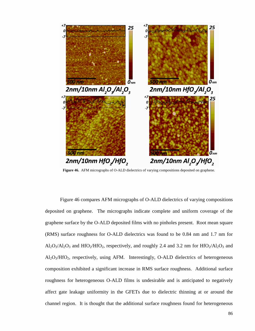
86
Figure 46. AFM micrographs of O-ALD dielectrics of varying compositions deposited on graphene.
Figure 46 compares AFM micrographs of O-ALD dielectrics of varying compositions
deposited on graphene. The micrographs indicate complete and uniform coverage of the
graphene surface by the O-ALD deposited films with no pinholes present. Root mean square
(RMS) surface roughness for O-ALD dielectrics was found to be 0.84 nm and 1.7 nm for
Al2O3/Al2O3 and HfO2/HfO2, respectively, and roughly 2.4 and 3.2 nm for HfO2/Al2O3 and
Al2O3/HfO2, respectively, using AFM. Interestingly, O-ALD dielectrics of heterogeneous
composition exhibited a significant increase in RMS surface roughness. Additional surface
roughness for heterogeneous O-ALD films is undesirable and is anticipated to negatively
affect gate leakage uniformity in the GFETs due to dielectric thinning at or around the
channel region. It is thought that the additional surface roughness found for heterogeneous

87
gate stacks could be a result of a rough interfacial region between the EBPVD seed and ALD
dielectric. Figure 47 shows TEM cross-sections of O-ALD gate stacks of various
seed/dielectric combinations.104
Figure 47. TEM micrographs show the interface between oxide seed and ALD dielectric for Al2O3/Al2O3 (d), HfO2/Al2O3
(e), Al2O3/HfO2 (f), and HfO2/HfO2 (g) gate stacks, where the heterogeneous O-ALD films (e) and (f) produced a
particularly rough interfacial region. The scale bar is 3 nm in length. Adapted from Ref. [104].
Although Figures 47a and 47d lack the contrast to discern any interfacial region
between the seed and dielectric overlayer, Figures 47b and 47c illustrate a rough interfacial
region at the seed-dielectric overlayer interface. The significant reduction in RMS surface
roughness for homogeneous gate stacks coupled with the presence of a rough interfacial
region for heterogeneous dielectrics as discerned by TEM indicated that the heterogeneous

88
interface was likely a significant source of roughness in the O-ALD deposited dielectrics.
Any increase in interfacial roughness near the graphene channel is undesirable in that it may
lead to increased interface roughness scattering of carriers in the channel.
Additionally, Figure 47a shows the EGSi-dielectric interface and indicated that O-
ALD processing did not significantly alter the structure of the underlying graphene. The lack
of structural degradation with use of O-ALD dielectrics was supported by Raman analysis of
graphene before and after deposition of O-ALD dielectrics (Fig. 48). Figure 48 shows G and
D peaks of the EGSi before and after deposition of O-ALD dielectric.
Figure 48. Averaged Raman spectra for O-ALD gate dielectrics show that seed layers did not degrade the underlying
graphene structurally. Adapted from Ref. [104].

89
The plotted spectra were averaged over several hundred locations across the samples,
after which each spectra was normalized to achieve an equivalent intensity G peak. The low
D/G ratio for the as-grown sample indicated high crystalline quality of the epitaxial
graphene. Additionally, the lack of any significant change in the D/G ratio with deposition
of dielectric by O-ALD (Fig. 48) indicated that the O-ALD deposition technique did not
significantly alter the structure of the underlying graphene. Similar results were found for
both metal seeded80
and EBPVD dielectrics that underwent Raman analysis. Although an
increase in D/G peak ratio was not found for O-ALD or EBPVD dielectrics in this work or
most M-ALD dielectrics in previous work (Ref. [80]), it should be noted that M-ALD
dielectrics using a tantalum metal seed did produce a large change in the D/G peak ratio.
This change was attributed to the large change in unit cell volume with oxidation and was
confirmed through TEM to have a highly destructive effect on the underlying graphene.
3.3.2 – Effect of Dielectric Overlayers on Carrier Transport
Hall effect measurements were used to evaluate the effect of seed layer and dielectric
overlayer on carrier transport within the graphene by measuring carrier density and Hall
mobility before and after deposition of the dielectric overlayer. Dielectric overlayers were
found to affect Hall mobility (Hall) as well as carrier concentration (ns), as shown in Figure
49. As-grown samples (black symbols) exhibited Hall of 700 – 1100 cm2/V·s and ns of 5 –
8x10¹²
cm-2
(n-type), typical of Si-face EG.105,106
The overall variation in as-grown carrier
concentration and Hall mobility found between samples indicated the challenge of obtaining
uniform doping across multiple samples, although samples prepared in a single run often
showed little variation.

90
Figure 49. Evaluation of Hall and ns (a) indicated that deposition of high- dielectrics by O-ALD and EBPVD can lead to
improved Hall through dielectric screening. Adapted from Ref. [104].
From Figure 49, we see that as-grown samples appeared to follow a
trend (black dashed line), where samples that were more heavily doped (n-type) were found
to have reduced mobility. Such a trend has been previously reported for Si-face EG,105
although it was unclear from the un-gated measurements whether this trend was due only to a
change in carrier concentration or also a change in sample quality. In order to determine the
actual Hall dependency on ns, gated Hall effect measurements were performed on samples
utilizing O-ALD deposited dielectric films. These samples utilized a duplicate process to
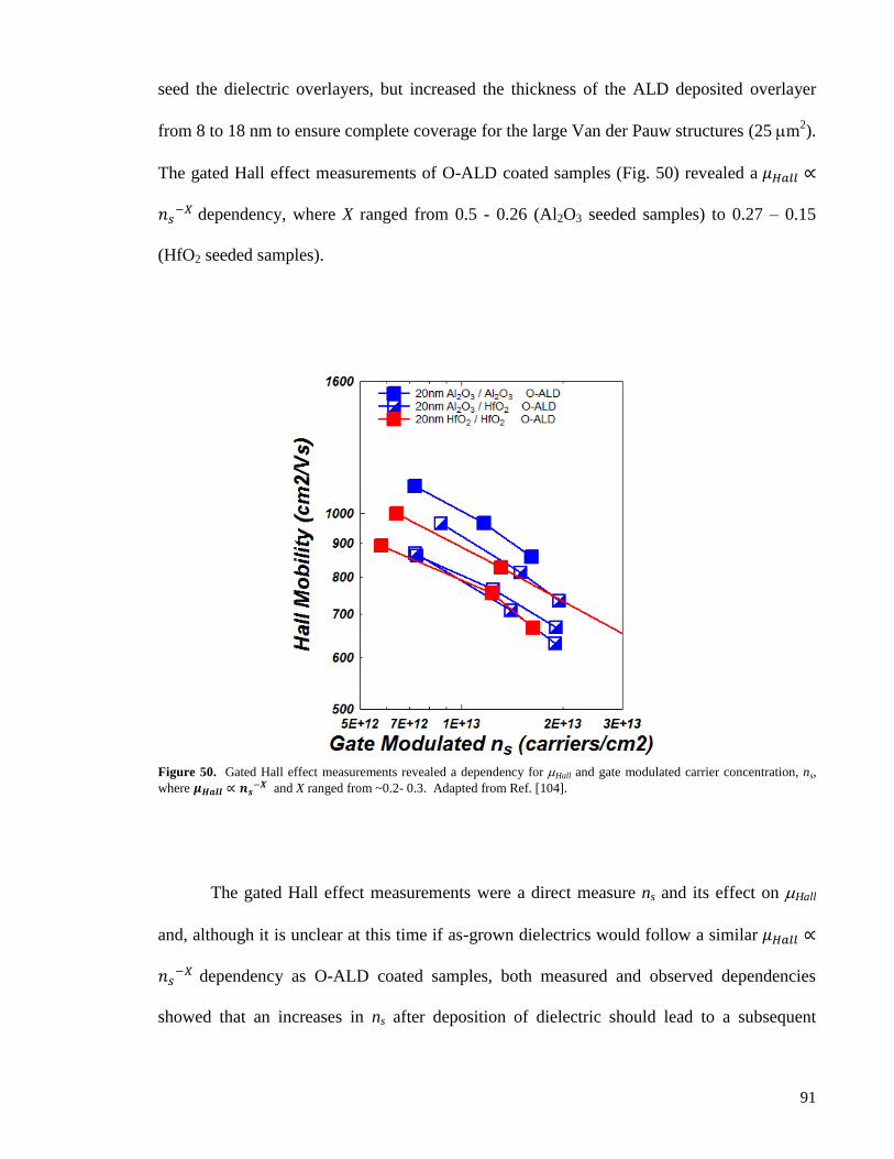
91
seed the dielectric overlayers, but increased the thickness of the ALD deposited overlayer
from 8 to 18 nm to ensure complete coverage for the large Van der Pauw structures (25 m2).
The gated Hall effect measurements of O-ALD coated samples (Fig. 50) revealed a
dependency, where X ranged from 0.5 - 0.26 (Al2O3 seeded samples) to 0.27 – 0.15
(HfO2 seeded samples).
Figure 50. Gated Hall effect measurements revealed a dependency for Hall and gate modulated carrier concentration, ns,
where and X ranged from ~0.2- 0.3. Adapted from Ref. [104].
The gated Hall effect measurements were a direct measure ns and its effect on Hall
and, although it is unclear at this time if as-grown dielectrics would follow a similar
dependency as O-ALD coated samples, both measured and observed dependencies
showed that an increases in ns after deposition of dielectric should lead to a subsequent

92
decrease in Hall, unless deposited dielectrics also acted to modify the scattering physics for
charge carriers within the graphene.
In this thesis all dielectrics were found to cause an increase in ns. This phenomenon
was likely due to the presence of oxygen vacancies or other charged defect complexes which
doped the graphene through a charge transfer process.79,107
Although all dielectrics caused an
increase in ns not all dielectrics subsequently caused a decrease in Hall. Figure 49 shows that
high- seeded dielectrics deposited by EBPVD (orange and blue circles) and by O-ALD
(filled and half-filled red and blue squares) caused both an increase in Hall and an increase in
ns. Conversely, low- seeded dielectrics deposited by O-ALD (SiO2/HfO2; half-filled green
squares) led to decreased Hall with increased ns.
Comparing the high- and low- seeded dielectrics, the high- seeds, in effect,
simply acted to shift the dependency upwards from and in parallel with the
low- dependency, similar to the case of high- solvents on exfoliated graphene.83
The
increase of Hall with deposition of high- was attributed to dielectric screening,81–85
signifying a reduction in scattering by remote charged impurities, and represented the first
time such an increase has been observed using conventional deposition techniques on EG.
Compared to previous work using M-ALD, it is thought that the use of direct deposited oxide
seed in O-ALD deposited films helps to preserve transport properties in the EG in order that
dielectric screening is not masked by a degradation of mobility.
Assuming the measured power dependencies of the O-ALD coated
samples were also valid for as-grown samples, one can make a rough estimation of the
change in Hall with deposition of dielectric. This is achieved by fitting the measured average
dependency to each individual pair of Hall and ns data points. The change in Hall could then
be estimated by calculating the percent change between as-grown and post-dielectric Hall at
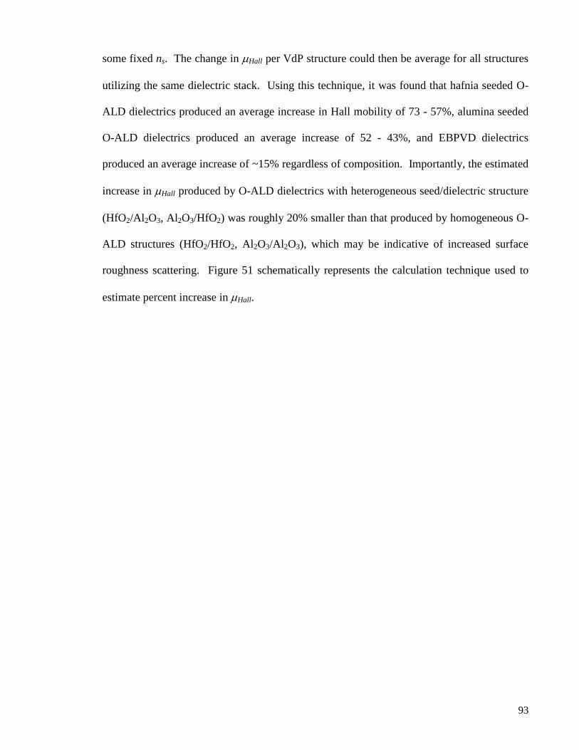
93
some fixed ns. The change in Hall per VdP structure could then be average for all structures
utilizing the same dielectric stack. Using this technique, it was found that hafnia seeded O-
ALD dielectrics produced an average increase in Hall mobility of 73 - 57%, alumina seeded
O-ALD dielectrics produced an average increase of 52 - 43%, and EBPVD dielectrics
produced an average increase of ~15% regardless of composition. Importantly, the estimated
increase in Hall produced by O-ALD dielectrics with heterogeneous seed/dielectric structure
(HfO2/Al2O3, Al2O3/HfO2) was roughly 20% smaller than that produced by homogeneous O-
ALD structures (HfO2/HfO2, Al2O3/Al2O3), which may be indicative of increased surface
roughness scattering. Figure 51 schematically represents the calculation technique used to
estimate percent increase in Hall.
94
Figure 51. The measured dependencies for the HfO2/HfO2 and Al2O3/Al2O3 samples from Fig. 48 are plotted along with
Hall effect data for the O-ALD and as-grown samples from Fig. 47 showing an improvement in Hall mobility due to
dielectric screening. Adapted from Ref. [104].
The estimated changes in mobility for O-ALD dielectrics were slightly lower than
those predicted by theory. In Ref. [83], the suppression factor, S, is a result of application of
the Born approximation while modeling the scattering potential for a Coulombic scatterer. S
is dependent on the effective relative permittivity, , where s and are the
dielectric constants of the substrate and a dielectric coating of at least a few nanometers,
respectively. Adapting the effective relative permittivity equation to Al2O3/Al2O3 (r ~7,
from capacitance measurements) and HfO2/HfO2 (r ~16, from capacitance measurements)

95
on a SiC substrate (r ~10; 6H polymorph22
) and solving for the suppression factor should
result in ~1.6x and ~2.5x increases in Hall, respectively.
EBPVD-only dielectrics exhibited a reduced improvement in Hall relative to O-ALD
dielectrics (~15% as compared to 50 – 65%). This reduced improvement could be the result
of a higher intrinsic defect concentration in these films relative to the O-ALD films leading
to increased remote charged impurity scattering. The presence of a large concentration of
charged defects in the EBPVD films was supported by thickness dependent measurements of
ns that suggested increased defect concentration with continued use of the EBPVD technique.
Figure 52 plots fractional change in Hall mobility versus fractional change in carrier density
(Hall/0 versus ns/n0 where 0 and n0 are the as-grown Hall and ns) for EBPVD HfO2
samples of varying thickness.
Figure 52. Normalized Hall effect data (Hall/0 and ns/n0 where 0 and n0 are as-grown Hall mobility and carrier
concentration, respectively). Adapted from Ref. [104].
96
For 5 nm thick EBPVD HfO2 films, a small increase in ns from as-grown of 10% was
found which increased to 40% for 10 nm thick films (Fig. 52). The increase in ns was also
accompanied by an expected decrease in Hall (also shown in Fig. 49). Fallahazad et al
showed a similar dependence on dielectric thickness for M-ALD dielectrics on exfoliated
graphene,79
where a decrease in mobility was reported that was attributed to an increase in
the charged impurity concentration with increasing thickness due to a charge transfer process
between the graphene and oxygen vacancies within the dielectric. While no mobility
decrease was found for EBPVD deposited dielectrics of different thicknesses in this work, it
is thought that a similar charge transfer process was responsible for the thickness dependence
of ns and might be indicative of a large defect concentration in these films. The lack of
mobility degradation with thickness for the EBPVD dielectrics in this work was likely due to
the lower intrinsic mobility of the EG system ( ~1000) as compared to the exfoliated
graphene on SiO2 studied by Fallahazad et al ( ~10000), or due to a higher defect
concentration in M-ALD dielectrics relative to EBPVD.
3.4 – DC Performance of Graphene FETs
Hall effect measurements for O-ALD and EBPVD dielectrics clearly indicated that
successful integration of a top-gate dielectric is possible without disrupting the transport
properties of EG and that proper choice and deposition of dielectrics are critical in optimizing
the performance of top-gate dielectrics on EG. However, in addition to optimizing the effect
of the overlayer on transport properties, the choice of material and deposition technique must
produce top-gates that satisfy the main functions of a gate dielectric, which are to sufficiently

97
isolate the channel from the gate and to capacitively couple the gate to the channel. An
investigation of the DC performance of the GFETs utilizing O-ALD and EBPVD gate
dielectrics was performed in order to compare the two techniques and the various gate
compositions for use in graphene based transistors.
3.4.1 – Effect of Dielectric on Leakage and Gate Modulation of Carriers
While the majority of the O-ALD gate stacks averaged 5x10-12
– 8x10-12
A/m2,
leakage currents for O-ALD HfO2/Al2O3 gates exhibited significant variability, ranging from
2x10-11
to 7x10⁻⁷
A/m2 (Vgs=3V) for different dimension GFETs with different degrees of
gate overlap. The variability in gate leakage for HfO2/Al2O3 gated GFETs was attributed to a
high RMS roughness relative to others. The small amount of gate leakage current for the
majority of O-ALD gated GFETs confirmed oxide seeding as a robust functionalization
technique ensuring uniform coverage of ALD dielectrics. Most gate stacks exhibited hard
breakdown at fields ranging between 4 – 9 MV/cm and with little correlation to composition
or deposition technique. For breakdown at this field strength, B-mode failure was
expected108
and suggested the presence of dielectric thinning, confirming AFM results
indicating thickness variability on the order of ±2 nm. Table 5 summarizes the gate leakage
through the deposited dielectrics, where a range of Ileak is presented representing the average
gate leakage through over 100 GFETs of various device dimensions.

98
Table 5. Summary of gate leakage through gate dielectrics deposited by various techniques and exhibiting various
compositions
deposition technique seed / dielectric combination Ileak @ Vgs=3V (A/m2)
O-ALD HfO2 / HfO2 5.6x10⁻¹² - 8.4x10⁻¹²
O-ALD HfO2 / Al2O3 1.7x10⁻¹¹ - 6.7x10⁻⁷
O-ALD Al2O3 / Al2O3 4.4x10⁻¹² - 7.3x10⁻¹²
O-ALD Al2O3 / HfO2 5.8x10⁻¹² - 8.8x10⁻¹²
Besides isolating the channel from the gate metallization, the gate dielectric must also
act to capacitively couple the gate contact to the channel so that the carrier concentration in
the channel can be modulated be effectively modulated. Table 6 summarizes the ability of
the investigated dielectrics to perform this task, showing Cox / q, , and n0, where is
defined from with ns as the carrier density in the channel, Vgs as the
applied gate bias, and n0 as the carrier density at zero-bias conditions.. In this way, is a
measure of the number of carriers that are modulated by an applied gate voltage. Ideally, Cox
/ q and should be equivalent, although the effects of quantum capacitance, traps, and non-
idealities all contribute to degrade from its ideal value. was extracted from gated Hall
effect measurements at room temperature in ambient conditions (Fig. 50).
Table 6. Carrier modulation for O-ALD gates of varying seed/overlayer combination
seed / dielectric combination
Cox / q
(e-/Vx1012)
a
(e-/V x 1012)
n0 b
(e-/ cm2)
HfO2 / HfO2 7.5 2.12 5.5x10¹²
HfO2 / Al2O3 6.3 1.43 5.6x10¹²
Al2O3 / Al2O3 5.0 1.57 7.2x10¹²
Al2O3 / HfO2 5.6 2.27 8.2x10¹²
99
Comparing the Cox / q and values listed in Table 6, it is clear that the measured
dependency of ns on Vgs was significantly less than that anticipated by measurements of Cox.
This discrepancy was attributed to a significant density of traps within the as-deposited gate
dielectrics due to the fact that quantum capacitance effects are anticipated to be small at such
high carrier concentrations (away from the low DOS at the Dirac point).
3.4.2 – Effect of Dielectric on Direct Current Measurements of GFETs
Direct current (DC) measurement of GFETs utilizing O-ALD and EBPVD gate
dielectrics were compared, confirming the benefits of high- EBPVD and O-ALD as
techniques for optimizing GFET performance. Figure 53 plots the transfer curves (Ids-Vgs
sweeps) of four different GFETs that utilized various different gate dielectrics. In the figure,
the high drive current and large modulation of the GFETs utilizing high- EBPVD and O-
ALD dielectrics are contrasted with the low drive current and small modulation of the GFET
utilizing a low- O-ALD dielectric.

100
Figure 53. Comparison of transfer curves of GFETs utilizing four different gate dielectrics. Adapted from Ref. [104].
As can be seen in Fig. 53, the combined effects of doping by the both the SiC
substrate and the deposited gate dielectrics resulted in GFETs that were heavily doped n-
type. The doping was so severe as to cause the NP to be inaccessible for most devices in this
thesis, even with extreme biasing of the device, which caused significant dielectric
breakdown and degraded performance of the GFETs.
Due to process variability and scatter in the results, peak transconductance (gm,max)
and peak drive current, Idss (Ids @ Vgs=3V, Vds=1V) were extracted from Ids-Vgs sweeps for
more than 500 devices utilizing various gate dielectrics and these extracted values were
plotted (Fig. 54).

101
Figure 54. Plot of peak transconductance versus peak drive current for GFETs utilizing gate dielectrics deposited by
EBPVD and O-ALD techniques. Adapted from Ref. [104].
The plot of peak transconductance versus peak drive current is sectioned into three
regions by black dotted lines (Fig. 54). The left-most region represents the poorest
performing devices while the right-most region represents the best performing devices.
GFETs utilizing low- SiO2 seeded O-ALD gates (Fig. 52; left-most section) exhibited
average Idss < 50 A/m and average gm,max < 10 S/m and represented the lowest
performance GFETs in this work. Low Idss and gm,max for SiO2 seeded O-ALD was attributed
to reduced mobility and increased ns relative to high- seeded gates (Fig. 49). Additionally,
high contact resistances (Rc) were found for this sample, where the oxygen plasma pre-
treatment was omitted. For all other samples, the use of plasma pre-treatment reduced Rc to
less than 200 -m, making contact resistance negligible under depletion conditions and
102
roughly 20% of the total resistance under accumulation. For the case of SiO2 seeded GFETs,
it iss anticipated that reduction of Rc should lead to a shift in the average Idss and gm,max closer
to 100 A/m and 20 S/m in accord with the highest performing SiO2 seeded GFETs. On
the other hand, GFETs utilizing high- EBPVD or high- seeded heterogeneous O-ALD
gates (Fig. 54; middle section) showed a 3-4x increase in Idss to 340 – 440 A/m and gm,max
to 40 – 70 S/m, with 5 nm EBPVD HfO2 gated GFETS displaying gm,max up to 140 S/m.
Homogeneous O-ALD gated GFETs (Fig. 54; right-most section) exhibited exceptional FET
characteristics with average Idss= 550 – 780 A/m and average gm,max = 66 – 134 S/m
depending on gate composition. Of the homogeneous O-ALD gated GFETs, HfO2/HfO2
GFETs were found to be superior to all others with Idss up to 971 A/m and gm,max up to 175
S/m. The increase in performance for GFETs utilizing high- EBPVD and high- O-ALD
dielectrics was attributed to a reduction of remote charged impurity scattering through
dielectric screening, leading to increased carrier mobility. The superior performance of
homogeneous O-ALD gated GFETs relative to heterogeneous O-ALD was attributed to
removal of the seed/overlayer interface which was thought to negatively affect carrier
transport in the channel through increased interface roughness scattering.
Transfer curve hysteresis in O-ALD GFETs ranged from 0.5 – 0.7 V with no
statistically significant trending according to gate composition. Additionally, we found an
increase in hysteresis for EBPVD gates to 1V, which was in agreement with a higher density
of charge traps for EBPVD dielectrics relative to O-ALD. The passivation or reduction of
these traps by thermal processing or optimized reactive depositions is anticipated to
significantly reduce hysteresis.
Additionally, we note that Al2O3 seeded O-ALD dielectrics led to reduced gm,max
relative to HfO2 seeds at a given Idss. This was attributed to a difference in the NP between
103
the HfO2 and Al2O3 coated samples, where a change in the intrinsic ns at zero-bias conditions
(Table 6) leads to a shift in the NP. For Figure 54, gm,max and Idss are both dependent on the
gate capacitance (Cox), eff, and carrier density according to and
, respectively. Therefore,
, the slope of the
regression plotted in Fig. 54 is related to if and only if gm,max and Idss occur at
equivalent bias conditions. Although gm,max and Idss generally refer to different points on the
transfer curve, the overall similarity between transfer curves leads to a constant relationship
between gm,max and Idss for the different O-ALD GFETs. This relationship means that,
approximately,
. Therefore, the change in slope between Al2O3
and HfO2 seeded regressions in Figure 54 can be explained by the fact that the Al2O3 seeded
gates are displaced farther from the NP than the HfO2 seeded gates under the same bias
conditions (Table 6, n0). The EBPVD GFETs, which are shown to have the smallest zero-
bias condition ns after deposition of gate (Fig. 49), also show the steepest slope (smallest
magnitude |Vgs – VNP|).
3.4.3 – Effect of Heterogeneous O-ALD Dielectrics on DC GFET Performance
The difference in performance between homogeneous and heterogeneous high-
seeded O-ALD gated FETs highlighted in Figure 52 and in estimation of change in Hall (Fig.
51) illustrates a key consideration for gate dielectric implementation: the effect of
seed/overlayer interface on carrier transport. Figure 55 compares the homogeneous and
heterogeneous high- seeded O-ALD gated GFETs, showing representative transfer curves
for O-ALD gated GFETs of varying seed/overlayer composition.

104
Figure 55. Transfer curves of four representative GFETs utilizing high- O-ALD gates illustrating increased Idss and gm,max
for GFETs utilizing homogeneous gate stacks. Adapted from Ref. [104].
Evident from Figure 55, heterogeneous gate dielectrics led to a decrease in Ids of more
than 30% compared to homogeneous gate dielectrics using the same seed material. The
absolute difference in average (post-dielectric) Hall and ns between samples with the same
oxide seed was < 4% (Fig. 49) and does not provide sufficient explanation for the differences
found in Ids.
Alternatively, the effective mobility (eff) of the GFETs can be extracted using a
simple charge control model:
, where Jds, is drain current
normalized by width,
is the gate capacitance normalized by area, Vgs is the applied gate
bias, VNP is the neutrality point (NP), and Vds is the driving voltage.63
In this work, the charge

105
control model was modified to become , where n0 is the
measured intrinsic ns at zero-bias conditions (Table 6, n0) and relates the charge carrier
density to the applied gate bias (Table 6, ) and is extracted from gated Hall effect
measurements at room temperature in ambient conditions. The modified model alleviates the
VNP constraint by directly sampling the carrier concentration at zero-bias conditions and uses
gated Hall effect measurements in place of Cox to make a more accurate estimation of carrier
density in the channel in the presence of a large number of traps and any quantum
capacitance effects. The model does not address contact resistance, although Rc was found to
be uniform between the high- seeded O-ALD samples. Figure 56 plots eff as a function of
ns and provides evidence that the degraded performance of heterogeneous dielectric GFETs
was the result of an approximate 40 – 30% degradation in eff compared to homogeneous
gate stacks.

106
Figure 56. Extracted eff plotted as a function of ns confirms a degradation in eff of 30 – 40% for GFETs with
heterogeneous O-ALD gate dielectrics. Adapted from Ref. [104].
Although Hall effect measurements show little change between heterogeneous and
homogeneous O-ALD dielectrics, it is speculated that interface roughness scattering had a
greater impact on GFET measurements and only minimally impacted Hall effect
measurements. The strong dependency of interface roughness scattering on carrier energy,109
yet weak dependency of remote charged impurity scattering on carrier energy109
help to
explain why the overall contributions of these two scattering processes could change
significantly between Hall effect and DC FET characterization at high drain biases.
Therefore, the degradation of eff for heterogeneous O-ALD dielectrics was attributed to
surface roughness scattering, although further work to model the scattering physics for this

107
system is necessary in order to develop a complete understanding of how the heterogeneous
gate dielectric interface impacts transport in GFETs.
3.5 – Small Signal Performance of Graphene FETs
Extrinsic H21 was extracted from high- O-ALD gated GFETs with gate dimensions
W=10 m and L=1 m. More than 5 GFETs were characterized for each of the four different
gate stacks (HfO2/HfO2, HfO2/ Al2O3, Al2O3/ Al2O3, and Al2O3/HfO2). Extrinsic current gain
was extracted for each GFET for Vds=1, 2, and 3V while Vgs was swept from -3 to -2V (5
points). H21 is plotted for representative devices under these bias conditions in Figures 57,
58, 59, and 60.
Figure 57. H21 extracted from S-parameters of a HfO2/HfO2 O-ALD gated GFET at various bias conditions.

108
Figure 58. H21 extracted from S-parameters of a HfO2/Al2O3 O-ALD gated GFET at various bias conditions.
Figure 59. H21 extracted from S-parameters of a Al2O3/Al2O3 O-ALD gated GFET at various bias conditions.

109
Figure 60. H21 extracted from S-parameters of a Al2O3/HfO2 O-ALD gated GFET at various bias conditions.
Figure 61 summarizes the small signal results. In this figure, both the average
maximum and average minimum extracted fT is plotted as a function of Vds for the high- O-
ALD gated GFETs utilizing the four different gate stack combinations. A unique curve fill is
then applied between the maximum and minimum curves.

110
Figure 61. Average extracted fT as a function of Vds. fT is plotted as a range (curve fill) showing the average maximum and
minimum fT measured as Vgs was varied between -3 and -2 V.
Extrinsic small signal current gain cutoff frequency (fT) was found to increase with
increasing drive voltage for all combinations of O-ALD dielectric. The increase in fT was
found to be approximately linear with Vds, showing an approximate 2x increase in fT as Vds
was increased from -1 to -3 V. Similar to DC performance of GFETs, the presence of a
seed/overlayer interface was found to negatively impact fT, where GFETs utilizing
homogeneous O-ALD gate dielectrics exhibited fT that was enhanced by 10 – 70%. Figure
62 plots the increase in maximum and minimum fT as a function of Vds for the GFETs
utilizing HfO2 and Al2O3 seeded O-ALD gate dielectrics.

111
Figure 62. Percent increase in maximum (left) and minimum (right) fT with use of homogeneous O-ALD deposited gate
dielectric as a function of Vds.
Although use of homogeneous gate dielectric was found to increase both maximum
and minimum fT for all investigated bias conditions, Figure 62 shows that the percent
increase in fT degraded as Vds was increased from -1 to -3V. Regardless, homogeneous gate
stacks outperformed heterogeneous gate stacks and demonstrate extrinsic fT > 2 GHz at
Vds=1V and up to 5.8 GHz at Vds=3V. Figure 63 plots |H21| as a function of frequency for
representative O-ALD gated GFETs biased close to peak transconductance.

112
Figure 63. Extrinsic small signal current gain as a function of frequency for GFETs demonstrated that RF performance
follows a similar trend as DC FET performance, where heterogeneous composition gate dielectrics led to a lower in fT.
Adapted from Ref. [104].
Based on DC performance of the O-ALD gated GFETs, the extrinsic RF performance
of homogeneous HfO2/HfO2 gated GFETs was expected to surpass all others; however, the
results indicated similar performance for both HfO2/HfO2and Al2O3/Al2O3 seeded GFETs,
with the highest recorded fT demonstrated using an Al2O3/Al2O3 gated device. The similar
performance between the homogeneous gated was likely the result of device processing
variation between samples. Although measured fT should ideally be a measure of mobility,
extrinsic GFET measurements may deviate from direct measurement as a result of parasitic
capacitances and resistances, which may vary due to processing variation. None-the-less,
Figure 63 clearly shows that the presence of a heterogeneous dielectric in GFETs can
significantly degrade RF performance.

113
Chapter Four: Conclusions
In this thesis, materials integration of metals and dielectrics with epitaxial graphene
was investigated. Various contact metals, pre-treatments, and post-treatments were
compared and a reproducible, robust process for producing low specific contact resistivity
metal contacts to epitaxial graphene was developed. Similarly, various gate dielectrics and
methods of deposition were investigated and a reproducible, robust technique for the
deposition of thin, high-k gate dielectrics on epitaxial graphene was developed. Importantly,
this method not only produces uniform, conformal, and robust gate dielectrics, but also leads
to an improvement in the transport properties of the underlying graphene, which was
attributed to dielectric screening and a reduction in remote charged impurity scattering.
Finally, the combination of optimized contacts and high-k gate dielectrics on epitaxial
graphene has allowed for the demonstration of high performance GFETs with excellent peak
drive currents, peak transconductances, and extrinsic current gain cutoff frequencies.
4.1 – Contacts
Through process optimization, we have demonstrated that the combination of a
“gentle” O2 plasma etch and subsequent heat treatment can result in superior contact
resistance values, which are necessary for high speed micro- and nano-electronic
technologies based on graphene. XPS was utilized to show that the use of an O2 plasma
resulted in removal of photoresist residue, but that, simultaneously, the graphene peak
intensity was severely attenuated and was replaced by a combination of C-C and C-O bonds
after use of O2 plasma. The degradation of the graphene exposed to O2 plasma was

114
confirmed by Raman spectroscopy; however, ρc was shown to increase despite damage to the
graphene to an average value of 4x10⁻⁷
Ohm-cm2 O2 plasmas lasting 30 – 90 sec.
Although we found little difference in specific contact resistance by varying the ideal
metal/graphene work function difference, the severely altered graphene structure and
chemistry prior to metallization complicates comparison to ideal models of the metal-
graphene interface.
4.2 – Gate Dielectrics
Several factors have been considered for integrating dielectrics with EG for device
applications including the importance of choice of seed layer on FET performance and
dielectric screening, as well as the effect of seed/dielectric interfaces on FET performance.
AFM was used to indicate complete and uniform coverage of the graphene surface by
EBPVD and O-ALD deposited films, although RMS surface roughness was shown to be on
the order of 1 – 2 nm. Raman spectroscopy and TEM micrographs were used to show that
O-ALD deposited films introduced minimal structural damage to the EG.
Hall effect measurements were utilized to show an improvement in Hall with
deposition of high- EBPVD and O-ALD dielectrics despite an increase in ns, which was
attributed to dielectric screening and a reduction in remote impurity scattering. The percent
increase in Hall mobility was estimated by assuming a dependency, where X
ranged from 0.5 - 0.15 and was extracted from gated Hall measurements in atmosphere of
VdP Hall structures gated with O-ALD dielectrics. With the assumed dependency, mobility
improvement was found to be 73 - 57% for hafnia seeded O-ALD dielectrics, 52 - 43% for
alumina seeded O-ALD dielectrics, and ~15% for EBPVD dielectrics regardless of
composition. The increase in Hall produced by O-ALD dielectrics with heterogeneous
115
seed/dielectric structure (HfO2/Al2O3, Al2O3/HfO2) was roughly 20% smaller than that
produced by homogeneous O-ALD structures.
The reduced improvement in Hall for EBPVD-only dielectrics relative to O-ALD
dielectrics was attributed to a higher intrinsic defect concentration in these films relative to
the O-ALD films leading to increased remote charged impurity scattering. The presence of a
large concentration of charged defects in the EBPVD films was supported by thickness
dependent measurements of ns that suggested increased defect concentration with continued
use of the EBPVD technique.
4.3 – DC Performance
GFET performance was characterized using Ids-Vgs sweeps and extracting several
parameters of interest, including peak drive current, peak transconductance, and maximum
leakage current.
Gate leakage currents averaging 5x10-12
– 8x10-12
A/m2 for the majority of O-ALD
gated GFETs confirmed oxide seeding as a robust functionalization technique ensuring
uniform coverage of ALD dielectrics. Hard breakdown ranging between 4 – 9 MV/cm was
found for the EBPVD and O-ALD gate dielectrics with little correlation to composition or
deposition technique, suggesting the presence of dielectric thinning and confirming AFM
results indicating thickness variability on the order of ±2 nm.
GFETs utilizing high- EBPVD and high- seeded O-ALD gates were demonstrated
and showed dramatically improved performance relative to GFETs utilizing low- seeded O-
ALD gates, attributed to dielectric screening. GFETs were demonstrated with drive currents
and transconductances up to 971 A/m and 235 S/m using a wafer scale growth

116
technique, where the excellent performance of high- seeded O-ALD gated GFETs was
attributed to the combination of low resistance contacts and enhanced transport through
dielectric screening. Additionally, DC performance of heterogeneous O-ALD gated GFETs
was shown to be degraded roughly 30 – 40% from homogeneous O-ALD gated GFETs.
Electrical characterization of GFETs using a charge control model was used to extract
eff, showing the degradation of effective mobility in the presence of a heterogeneous gate
stack. The degradation of effective mobility for heterogeneous gate stacks was attributed to
increased surface roughness scattering.
4.4 – Small Signal Performance
Small signal performance of O-ALD gated GFETs was characterized by extracting
the small signal current gain, H21, from the measured extrinsic scattering parameters.
Extrinsic small signal current gain cutoff frequency (fT) was found to increase with
increasing drive voltage for all combinations of O-ALD dielectric. The increase in fT was
found to be approximately linear with Vds. Similar to DC performance of GFETs, the
presence of a seed/overlayer interface was found to negatively impact fT, where GFETs
utilizing homogeneous O-ALD gate dielectrics exhibited fT that was enhanced by 10 – 70%.
Although DC characterization and Hall effect measurements suggested that
homogeneous HfO2 O-ALD gated GFETs should demonstrate the highest small signal
performance, this was not the case. Instead, both HfO2 and Al2O3 gated homogeneous O-
ALD GFETs showed similar performance, which was attributed to process variation during
device fabrication and the effects of parasitics on the extrinsic RF device performance.
117
Chapter Five: Future Work
Only a few years after the first reported graphene FET researchers have been able to
successfully incorporate them in low-noise amplifiers, frequency mixers, and frequency
multipliers. The rapid advance of graphene technology in only a few short years is a
testament to its phenomenal intrinsic properties and its potential as an electronic material for
use in advanced or novel applications. Although it is uncertain at this time whether graphene
will ultimately surpass III-V and Si semiconductors in the RF or digital application space, the
unique structure and properties of graphene present exciting opportunities in these and other
application spaces.
Although graphene transistors in recent years have reached an impressive intrinsic
current gain cut-off frequency (fT) of 300 GHz, the extrinsic performance of RF GFETs has
lagged behind intrinsic performance. The difference in extrinsic and intrinsic performance of
graphene FETs is a direct result of device parasitics. Parasitic resistances in the form of
contact resistances or un-gated portions of graphene combine to create high access
resistances that degrade RF performance. Additionally, un-optimized device designs might
lead to unacceptably high parasitic capacitances. Along with device parasitics, the limited
saturation behavior demonstrated by graphene devices and the in-ability to integrate top-
dielectrics without degradation of transport properties in the underlying graphene combine to
limit the ultimate achievable RF performance of graphene FETs by leading to high gd and
reduced mobility (low gm).
In this thesis, metal-graphene contacts and top-gate dielectrics were investigated as
components of the graphene-based FET. Optimized processes for the formation of contacts
and deposition of gate dielectrics were developed, yet, in order to push graphene-based
technologies forward, metal-graphene contacts and top-gate dielectrics on graphene must
118
continue to be optimized. Additionally, the weak-saturation of graphene devices, device
processing, and short-channel effects in graphene FETs must also be better understood. By
working to improve the material properties and utilizing optimized device architectures that
minimize parasitics and help to control short-channel effects, GFET RF performance can be
developed to its ultimate potential. Whether this will be enough to surpass conventional
semiconductors is unknown at this time, but graphene devices cannot be competitive with
current semiconductor devices without continued work to optimize and understand.
Following are several key areas of improvement that EGSi-based devices must
overcome in order to achieve high performance, wafer-scale graphene-based devices.
5.1 – Hydrogen Intercalation to Improve Carrier Mobility
Although use of sublimation allows for highly controllable, wafer-scale synthesis of
graphene on SiC substrates, the presence of a buffer layer on EGSi leads to distortion of the
Dirac cone and reduced transport properties relative to pristine exfoliated graphene. In order
to continue to advance the performance of epitaxial graphene, the removal, or passivation, of
the carbon buffer layer is desirable.
Recently, successful “cleaving” of the buffer layer in EGSi was achieved via hydrogen
intercalation.110111,112,113,114115
This process, which in its simplest form amounts to exposing
EGSi to molecular hydrogen at elevated temperatures, results in what is referred to as quasi-
free standing epitaxial graphene (QF-EGSi).110
The process allows for the passivation of the
carbon buffer layer that exists between the EGSi and SiC substrate by terminating the SiC
surface in H-bonds and converting the buffer layer into a single-layer of graphene. The
carrier mobility and transport properties of QF-EGSi are increased substantially over non-
119
hydrogen intercalated EGSi due to its more free-standing nature, confirmed by angle resolved
photoemission spectroscopy (ARPES) and Hall effect measurements.
The increase in transport properties found with hydrogen intercalation should lead
directly to improved DC and RF GFET performance through increased drive currents,
transconductances, and cutoff frequencies. Thus, the incorporation of hydrogen intercalation
into the process flow of GFET fabrication should be of paramount importance.
5.2 – Reducing Output Conductance
The large output conductance of graphene based devices is a result of weak-saturation
behavior. The weak saturation behavior of GFETs is a result of ambipolar conduction which
prevents pinch-off in the graphene channel. As the drain bias is increased, the channel is
depleted of one type of carrier and inverted to the other type, thus allowing for increased
drain current as the drain bias is increased. In order to maximize the RF performance of the
graphene-based FET, the large output conductance of the GFET must be reduced. Initially,
there are two ways to go about doing this.
The first method relies on the fact that a small saturation region plateau is observed in
the ideal GFET Ids-Vds curve as the channel is initially depleted of majority carriers by the
drain bias at the drain end of the channel, but before the drain bias increases to the point
where the carrier type is inverted. If the GFET is biased so that the device operates in this
regime, the output conductance can be reduced, leading to improved high frequency
performance and cutoff frequency.
The second method requires the utilization of a technique to open a bandgap in the
graphene. By opening a bandgap, the output conductance can be reduced by reducing
120
ambipolar conduction as the drain bias increases. Additionally, the opening of a bandgap
would also lead to improved on-off ratios. The combination of these two changes should
lead to improved transistor performance, although the opening of a bandgap might also act to
degrade the carrier mobility in the channel. As discussed in Chapter 1, there are several
techniques that might be used to open a bandgap in graphene.
5.3 – Optimizing GFET Design to Minimize Device Parasitics
In order to access the excellent intrinsic properties of graphene, the effect of device
parasitics must be minimized, including parasitic resistances due to un-gated portions of the
channel or un-optimized contacts and parasitic capacitances due to un-optimized device
structures. These parasitics act to reduce the device performance by limiting
transconductance and, ultimately, the extrinsic small signal performance.
In order to minimize the effects of parasitics, they must first be quantified and
characterized, requiring an extensive study of RF performance of GFETs of various gate
length, width, and source-drain spacing, as well as device processing, and their effects on
device parasitics. Such a study should make use of de-embed structures allowing device
parasitics can be extracted from extrinsic S-parameters so that the source or cause of such
parasitics might be discerned.
Continued optimization of the metal-graphene contact are anticipated to reduce
parasitic contact resistances, while the adoption of a self-aligned process or source-drain
extensions might be used to reduce the un-gated regions of the channel and reduce access
resistance. Further work to identify device architectures that minimize parasitic capacitances
or other device parasitics is necessary.
121
5.4 – Optimizing the Gate Dielectric Using Post-Processing
Although the results presented in this thesis show that use of O-ALD deposited gate
dielectrics can lead to a substantial improvement in transport properties (up to 70%) and DC
GFET performance, the significant amount of hysteresis present in Ids-Vgs curves suggest that
the dielectric-graphene interface can be improved.
The extent of hysteresis found for O-ALD and EBPVD gated GFETs combined with
a thickness dependence of mobility for EBPVD dielectrics suggest the presence of a large
degree of charge traps which contribute both to hysteresis and also to limiting carrier
mobility. The passivation or reduction of these traps or other defects that might exist within
the as-deposited dielectric should lead to improved carrier mobility and reduced hysteresis.
For silicon devices, utilization of post-processing techniques such as heat treatments
in forming gas have allowed for the reduction of such defects. Similarly, post-processing
heat treatments of dielectrics on graphene-based devices could lead to substantial
improvements in device performance. Therefore, work should continue to understand the
dielectric-graphene interface and how best to optimize it so as to achieve a low density of
charge traps and interface states, which degrade transistor performance.

122
References
1 Peierls, R.E. Quelques proprieties typiques des corpses solides. Ann. I. H. Poincare 1935
5, 177-222.
2 Landau, L.D. Zur Theorie der phasenumwandlungen II. Phys. Z. Sowjetunion 1937 11,
26-35.
3 Landau, L.D.; Lifshitz, E.M. Statistical Physics, Part I. Pergamon Press, Oxford, 1980.
4 Novoselov, K.S.; et al. Electric Field Effect in Atomically Thin Carbon Films. Science
2004, 306, 666-669.
5 Novoselov, K.S.; et al. Two-dimensional atomic crystals. Proc. Natl. Acad. Sci. USA 2005
102, 10451-10453.
6 Novoselov, K.S.; et al. Two-dimensional gas of massless Dirac Fermions in Graphene.
Nature 2005 438, 197-200.
7 Zhang, Y.; Tan, J.W.; Stormer, H.L.; Kim, P. Experimental Observation of the Quantum
Hall Effet and Berry’s Phase in Graphene. Nature 2005 438, 201-204.
8 Meyer, J.C.; et al. The structure of suspended graphene sheets. Nature 2007.
9 Stankovich, S.; et al. Graphene-based Composite Materials. Nature 2006 442, 282-286.
10 Geim, A.; et al. Graphene: Status and Prospects. Science 2009 324, 5934.
11 Heyrovska, R. Atomic Structures of Graphene, Benzene and Methane with Bond Lengths
as Sums of the Single, Double and Resonance Bond Radii of Carbon.
12 Lee, C.; Wei, X.; Kysar, J.W.; Hone, J. “Measurement of the Elastic Properties and
Intrinsic Strength of Monolayer Graphene.” Science 2008 321, 5887, 385-388.
13 Balandin, A.A.; Gosh, S.; Bao, W.; Calizo, I.; Tewldebrhan, D.; Miao, F.; Lau, C.N.
“Superior Thermal Conductivity of Single-Layer Graphene.” Nano Letters 2008 8, 3,
902-907.
14 Geim, A.K.; Novoselov, K.S. The Rise of Graphene. Nature Materials 2007 6, 183-191.
15 Wojtaszek, Magdalena. Graphene: A Two Type Charge Carrier System. MS Thesis,
Faculteit der Wiskunde en Natuurwetenshappen Technische Natuurkunde, Rijks
Universiteit Groningen. July 2009.
16 Adam, S.; Hwang, E.H.; Galitski, V.M.; Das Sarma, S. Proc. Natl. Acad. Sci. of America
2007 104, 47, 18392-18397.

123
17 Bolotin, K.I.; Sikes, K.J.; Jiang, Z.; Klima, M.; Fudenberg, G.; Hone, J.; Kim, P.; Stormer,
H.L. Ultrahigh Electron Mobility in Suspended Graphene. Solid State
Communications 2008 146, 351-355.
18 Chen, J.H.; Jang, C.; Xiao, S.; Ishigami, M.; Fuhrer, M. Intrinsic and Extrinsic
Performance Limits of Graphene Devices on SiO2. Nature Nanotech. 2008 3, 206-
209.
19 Dorgan, V.E.; Bae, M.H.; Pop, E. Mobility and Saturation Velocity in Graphene on SiO2.
Appl. Phys. Lett. 2010 97, 082112.
20 Akturk, A.; Goldsman N.; “Electron transport and full-band electron-phonon interactions
in graphene.” Journal of Applied Physics 2008, 103, 053702
21 Murali, R.; Yan, Y.; Brenner, K.; Beck, T.; Meindl, J.D. “Breakdown Current Density of
Graphene Nanoribbons.” Applied Physics Letters 2009 94, 2434114
22 Semiconductors on NSM. <www.ioffe.ru/SVA/NSM/Semicond/>.
23 Hernandez, Y.; et al. Nature Nano. 2008 3, 563.
24 Yu, Q.; Lian, J.; Siriponglert, S.; Li, H.; Chen, Y.P.; Pei, S.S. Graphene Segregated on Ni
Surface and Transferred to Insulators. Appl. Phys. Lett. 2008 93, 113103.
25 Wintterlin, J.; Bocquet, M.L. Graphene on Metal Surfaces. Surface Science 2009 603,
1841-1852.
26 Li, X.; Zhu, Y.; Cai, W.; Borysiak, M.; Han, B.; Chen, D.; Piner, R.D.; Colombo, L.;
Ruoff, R.S. “Transfer of Large-Area Graphene Films for High-Performance
Transparent Conductive Electrodes.” Nano Lett. 2009, 9, 12, 4359-4363.
27 Reina, A.; Jia, X.; Ho, J.; Nezich, D.; Son, H.; Bulovic, V.; Dresselhaus, M.S.; Kong, J.
“Large Area, Few-layer Graphene Films on Arbitrary Substrates by Chemical Vapor
Deposition.” Nano Lett. 2009, 9, 1, 30-35.
28 Levendorf, M.P; Ruiz-Vargas, C.S.; Garg, S.; Park, J. “Transfer-Free Batch Fabrication
of Single Layer Graphene Transistors.” Nano Lett. 2009, 9, 12, 4479-4483.
29 Emtsev, K.V.; Bostqick, A.; Horn, K.; Jobst, J.; Kellogg, G.L.; Ley, L.; McChesney, J.L.;
Ohta, T.; Reshanov, S.A.; Rohrl, J.; Rotenberg, E.; Schmid, A.K.; Waldmann, D.;
Weber, H.B.; Seyller, T. “Towards Wafer-size Graphene Layers by Atmospheric
Pressure Graphitization of Silicon Carbide.” Nature Materials 2009 8, 203-207.
30 Nakamura, S.; Kimoto, T.; Matsunami, H.; Tanaka, S.; Teraguchi, N.; Suzuki, A.
“Formation of Periodic Steps with a Unit-Cell Height on 6H-SiC (0001) Surface by
HCl Etching.” Appl. Phys. Lett. 2000, 76, 3412-3414.

124
31 Robinson, J.A.; Weng, X.; Trumbull, K.A.; Cavalero, R.; Wetherington, M.; Frantz, E.;
LaBella M.; Hughes, Z.; Fanton, M.; Snyder, D. “Nucleation of Epitaxial Graphene
on SiC(0001).” ACS Nano. 2010 4, 153-158.
32 Zhou, S.Y.; et al. Nature Mat. 2007 6, 770.
33 Kim, S.; Ihm, J.; Choi, H.J.; Son, Y.W. Phys. Rev. Lett. 2008 100, 176802.
34 Riedl, C.; Coletti, C.; Iwasaki, T.; Zakharov, A.A.; Starke, U. “Quasi-Free-Standing
Epitaxial Graphene on SiC Obtained by Hydrogen Intercalation.” Phys. Rev. Lett.
2009 103, 246804.
35 Robinson, J.A.; Wetherington, M.; Tedesco, J.L.; Campbell, P.M.; Weng, X.; Stitt, J.;
Fanton, M.A.; Frantz, E.; Snyder, D.; VanMill, B.L.; Jernigan, G.G.; Myers-Ward,
R.L.; Eddy, C.R.; Gaskill, D.K. “Correlating Raman Spectral Signatures with Carrier
Mobility in Epitaxial Graphene: A Guide to Achieving High Mobility on the Wafer
Scale.” Nano Lett. 2009 9, 2873-2876.
36 Orlita, M.; Faugeras, C.; Plochocka, P.; Neugebauer, P.; Martinez, G.; Maude, D.K.;
Barra, A.-L.; Sprinkle, M.; Berger, C.; de Heer, W.A.; Potemski, M. “Approaching
the Dirac Point in High-Mobility Multilayer Epitaxial Graphene.” Phys. Rev. Lett.
2008 101, 267601.
37 Zhang, Y.; et al. “Direct Observation of a Widley Tunable Bandgap in Bilayer
Graphene.” Nature 2009 459, 820-823.
38 Pereira, V.M.; Castro Neto, A.H.; Peres, N.M.R. “Tight-binding Approach to Uniaxial
Strain in Graphene.” Phys. Rev. B 2009, 80, 045401.
39 Yang, L.; et al. “Quasiparticle energies and band gaps in graphene nanoribbons.” Phys.
Rev. Lett. 2007, 99, 186801.
40 The International Technology Roadmap for Semiconductors
http://www.itrs.net/Links/2009ITRS/Home2009.htm (Semiconductor Industry
Association, 2009).
41 Schwierz, F. “Graphene Transistors.” Nature Nanotechnology 2010 5, 487.
42 Schwierz, F.; Liou, J.J. Modern Microwave Transistors – Theory, Design, and
Performance (Wiley, 2003).
43 Zhang, Q.; Lu Y.; Xing, H.G.; Koester, S.J.; Koswatta, S.O.; “Scalability of Atomic-
Thin-Body (ATB) Transistors Based on Graphene Nanoribbons.” Electron Device
Letters, IEEE 2010 31, Issue 6, 531-533
44 Meric, I.; Han, M.Y.; Young, A.F.; Ozylimaz, B.; Kim, P.; Shepard, K.L. “Current
saturation in zero-bandgap, top-gated graphene field-effect transistors.” Nature
Nanotechnology 2008 3, 654-659

125
45 Moon, J.S.; Curtis, D.; Bui, S.; Hu, M.; Gaskill, D.K.; Tedesco, J.L.; Asbeck, P.; Jernigan,
G.G.; VanMil, B.L.; Myers-Ward, R.L.; Eddy, C.R.; Campbell, P.,M.; Weng, X.;
“Top-gated epitaxial graphene FETs on Si-face SiC wafers with a peak
transconductance of 600mS/mm.” Electron Device Letters, IEEE 2010 31, No. 4,
260-262
46 Moon, J.S.; Curtis, D.; Zehnder, D.; Kim, S.; Gaskill, K.; Jernigan, G.G.; Myers-Ward,
R.L.; Eddy, C.R.; Campbell, P.M.; Lee, K.-M.; Asbeck, P. “Low-Phase Noise
Graphene FETs in Ambipolar RF Applications.” Electron Device Letters, IEEE
2011, 32, 3, 270-272
47 Lei Liao, Jingwei Bai, Rui Cheng, Yung-Chen Lin, Shan Jiang, Yongquan Qu, Yu Huang,
and Xiangfeng Duan; Sub-100 nm Channel Length Graphene Transistors; DOI:
10.1021/nl101724k
48 Lin, Y.M.; Dimitrakopoulos, C.; Jenkins, K.A.; Farmer, D.B.; Chiu, H.Y.; Grill, A.;
Avouris, Ph.; “100-Ghz transistors from wafer-scale epitaxial graphene.” Science
2010 327, 5966, 662
49 Moon, J.S.; et al. “Epitaxial-graphene RF Field-effect Transistors on Si-face 6H-SiC
Substrates. IEEE Electron Dev. Lett. 2009 30, 650-652.
50 Defense Advanced Research Projects Agency Broad Area Announcement: Carbon
Electronics for RF Applications (BAA07-50), June 2007
51Han Wang, Allen Hsu, Justin Wu, Jing Kong, and Tomas Palacios; IEEE ELECTRON
DEVICE LETTERS, VOL. 31, NO. 9, SEPTEMBER 2010
52 Yu-Ming Lin, Alberto Valdes-Garcia, Shu-Jen Han, Damon B. Farmer, Inanc Meric,
Yanning Sun, Yanqing Wu, Christos Dimitrakopoulos, Alfred Grill, Phaedon
Avouris, Keith A. Jenkins; Science 10, 1294-1297 (2011)
53 J. S. Moon, D. Curtis, D. Zehnder, S. Kim, D. K. Gaskill, G. G. Jernigan, R. L. Myers-
Ward,C. R. Eddy, Jr., P. M. Campbell, K.-M. Lee, and P. Asbeck; IEEE ELECTRON
DEVICE LETTERS, VOL. 32, NO. 3, MARCH 2011
54 Lemme, M.C.; Echtermeyer, T.J.; Baus, M.; Kurz, H. “A Graphene Field-effect Device.”
Ieee Electron Dev. Lett. 2007, 28, 282-284.
55 Liao, L. et al. High-speed graphene transistors with a self-aligned nanowire gate. Nature
467, 305–308 (2010).
56 Liao, L.; Bai, J.; Cheng, R.; Lin, Y.; Jiang, S.; Qu, Y.; Huang, Y.; Duan, X.; Sub-100 nm
Channel Length Graphene Transistors. Nano Lett., 2010, 10, 3952–3956
126
57 Rangel, N.; Seminario, J. Graphene Terahertz Generators for Molecular Circuits and
Sensors. J. Phys. Chem. A 2008, 112, 13699–13705
58 Ryzhii, V.; Dubinov, A.; Otsuji, T.; Mitin, V.; Shur,M. Terahertz lasers based on optically
pumped multiple graphene structures with slot-line and dielectric waveguides. J.
Appl. Phys. 2010, 107, 054505.
59 Venugopal, V.; Colombo, L.; Vogel, E.; Contact resistance in few and multilayer
graphene devices. Appl. Phys. Lett. 2010, 96, 013512
60 Nagashio, K.; Nishimura, T.; Kita, K.; Toriumi, A. Metal/Graphene Contact as a
Performance Killer of Ultra-high Mobility Graphene: Analysis of Intrinsic Mobility
and Contact Resistance. IEEE IEDM Conference 2009, 565-568
61 S. Russoa, S.; Craciuna, M.; Yamamotoa, M.; Morpurgoc, A.; Taruchaa, S. Contact
resistance in graphene-based devices. Physica E 2010, 4, 677-679
62 Moon, J.; Curtis, D.; Bui, S.; Marshall, T.; Wheeler, D.; Valles, I.; Kim, S.; Wang, E.;
Weng, X.; Fanton, M. Top-Gated Graphene Field-Effect Transistors Using Graphene
on Si (111) Wafers. IEEE Eectron. Dev. Lett. 2010, 31, 1193-1195
63 Moon, J.; Curtis, D.; Bui, S.; Hu, M.; Gaskill, D.; Tedesco, J.; Asbeck, P.; Jernigan, G.;
VanMil, B.; Myers-Ward, R.; Eddy, Jr., C.; Campbell, P.M. Top-gated epitaxial
graphene FETs on Si-face SiC wafers with a peak transconductance of 600 mS/mm.
IEEE Electron Device Lett. 2010, 31, 260–262
64 K. Nagashio, T. Nishimura, K. Kita and A. Toriumi; Contact resistivity and current flow
path at metal/graphene contact, Appl. Phys. Lett. 2010, 97, 143514
65 Giovannetti, G.; Khomyakov, P.A.; Brocks, G.; Karpan, V.M.; van den Brink, J.; Kelly,
P.J. “Doping Graphene with Metal Contacts.” Phys. Rev. Lett. 2008, 101, 026803.
66 Nagashio, K.; Nishimura, T.; Kita, K.; Toriumi, A. “Metal/Graphene Contact as a
Performance Killer of Ultra-high Mobility Graphene – Analysis of Intrinsic Mobility
and Contact Resistance –.” IEDM 2009, 565.
67 Chen, Z.; Appenzeller, J. “Gate Modulation of Graphene Contacts – On the Scaling of
Graphene FETs.” 2009 Symposium on VLSI Technology 2009 128-129.
68 Berdebes, D.; Low, T.; Sui, Y.; Appenzeller, J.; Lundstrom, M. “Substrate Gating of
Contact Resistance in Graphene Transistors.” Mesoscale and Nanoscale Physics
2011.
69 Wu, Y.Q.; Ye, P.D.; Capano, M.A.; Xuan, Y.; Sui, Y.; Qi, M.; Cooper, J.A.; Shen, T.;
Pandey, D.; Prakash, G.; Reifenberger, R. “Top-gated graphene field-effect-
transistors formed by decomposition of SiC.” Applied Physics Letters 2008 92,
092102
127
70 Kedzierski, J.; Hsu, P.-L.; Healy, P. Wyatt, P.W.; Keast, C.L.; Sprinkle, M.; Berger, C.;
de Heer, W.A. “Epitaxial Graphene Transistors on SiC Substrates.” IEEE
Transactions on Electron Devices. 2008 Vol. 55, No. 8
71 Lee, B.; Park, S.Y.; Kim,H.C.; Cho, K.J.; Vogel, E.M.; Kim, M.J.; Wallace, R.M.; Kim, J.
“Conformal Al2O3 Dielectric Layer Deposited by Atomic Layer Deposition for
Graphene-based Nanoelectronics.” Appl. Phys. Lett. 2008, 92, 203102
72 Lin,Y.M.; Jenkins, K.A.; Valdes-Garcia, A.; Small, J.P.; Farmer, D.B.; Avouris, P.
“Operation of Graphene Transistors at Gigahertz Frequencies.” Nano Lett. 2009, 9,
422
73 Wang, X.; Tabakman, S.M.; Dai, H. “Atomic Layer Deposition of Metal Oxides on
Pristine and Functionalized Graphene.” J. Am. Chem. Soc. 2008, 130, 8152.
74 Kim, S.; Nah, J.; Jo, I.; Shahrjerdi, D.; Colombo, L.; Yao, Z.; Tutuc, E.; Banerjee, S.K.
“Realization of a high mobility dual-gated graphene field-effect transistor with Al2O3
dielectric.” Applied Physics Letters 2009 94, 062107
75 Xu H.; Zhang, Z.; Wang, Z.; Wang, S.; Liang, X.; Peng, L.M. “Quantum Capacitance
Limited Vertical Scaling of Graphene Field-Effect Transistor.” ACS Nano 2011 Vol.
5, No. 3 2340-2347.
76 Farmer, D.B.; Chiu, H.Y.; Lin, Y.M.; Jenkins, K.A.; Xia, F.; Avouris, P. “Utilization of a
buffered dielectric to achieve high field-effect carrier mobility in graphene
transistors.” Nano Letters 2009 9, 12, 4474-4478
77 Liao, L.; Bai, J.; Qu, Y.; Lin, Y.C.; Li, Y.; Huang, Y.; Duan, X. “High-k oxide
nanoribbons as gate dielectrics for high mobility top-gated graphene transistors.”
Applied Physical Sciences 2010 107, 15, 6711-6715
78 Liao, L.; Lin, Y.C.; Bao, M.; Cheng, R.; Bai, J.; Liu, Y.; Qu, Y.; Wang, K.L.; Huang, Y.;
Duan, X. “High-speed graphene transistors with a self-aligned nanowire gate.”
Nature 2010 467, 7313, 305-308
79 Fallahazad, B.; Kim, S.; Colombo, L.; Tutuc, E. “Dielectric thickness dependence of
carrier mobility in graphene with HfO2 top dielectric.” Applied Physics Letters 2010
97, 123105
80 Robinson, J.A.; Labella, M.; Trumball, K.A.; Weng, X.J.; Cavelero, R.; Daniels, T.;
Hughes, Z.; Hollander, M.J.; Fanton, M.; Snyder, D.; “Epitaxial Graphene Materials
Integration: Effects of Dielectric Overlayers on Structural and Electronic Properties”
ACS Nano 2010 4 (5), 2667-2672
128
81 Hwang, E.H.; Sarma, S.D. “Dielectric function, screening, and plasmons in two
dimensional graphene.” Physical Review B 2007 75, 205418
82 Konar, A.; Fang, T.; Jena, D. “Effect of high-k gate dielectrics on charge transport in
graphene-based field effect transistors.” Physical Review B 2010 82, 115452
83 Ponomarenko, L.A.; Yang, R.; Mohiuddin, T.M.; Katsnelson, M.I.; Novoselov, K.S.;
Morozov, S.V.; Zhukov, A.A.; Schedin, F.; Hill, E.W.; Geim, A.K. “Effect of a
High-k Environment on Charge Carrier Mobility in Graphene.” Physical Review
Letters 2009 102, 206603
84 Chen, F.; Xia, J.; Ferry, D.K.; Tao, N. “Dielectric screening enhanced performance in
graphene FET.” Nano Letters 2009 9, 7, 2571-2574
85 Jang, C.; Adam, S.; Chen, J.-H.; Williams, E.D.; Sarma, S.D.; Fuhrer, M.S. “Tuning the
effective fine structure constant in graphene: opposing effects of dielectric screening
on short- and long-range potential scattering.” Physical Review Letters 2008 101,
146805
86 Ni, Z.H.; Wang, H.M.; Ma, Y.; Kasim, J.; Wu, Y.H.; Shen, Z.X. ACS Nano 2008, 2,
1033-1039.
87 Lee, B.K.; Park, S.Y.; Kim, H.C.; Cho, K.; Vogel, E.M.; Kim, M.J.; Wallace, R.M.; Kim,
J.Y. Applied Phys. Lett. 2008, 92, 203102.
88 Wang, X.R.; Tabakman, S.M.; Dai, H.J. “Atomic Layer Deposition of Metal Oxide on
Pristine and Functionalized Graphene.” Journal of Amer. Chem. Soc. 2008 130,
8152-8153.
89 Liao, L.; Duan, Z. “Graphene-dielectric Integration for Graphene Transistors.” Materials
Science and Engineering R 2010, 70, 354-370.
90 Robinson, J.A.; Wetherington, M.; Tedesco, J.L.: Campbell, P.M.; Weng, X.; Stitt, J.;
Fanton, M.; Frantz, E.; Snyder, D.; VanMil, B.L.; Jernigan, G.G.; Meyers-Ward,
R.L.; Eddy, C.R.; Gaskill, D.K.; “Correlating raman spectral signatures with carrier
mobility in epitaxial graphene: a guide to achieving high mobility on the wafer scale”
Nano Letters 2009, 9, 2873-2876
91 <en.wikipedia.org/wiki/File:Atomic_force_microscope_block_diagram.svg>.
92 Ferrari, A.C.; Meyer, J.C.; Scardaci, V.; Casiraghi, C.; Lazzeri, M.; Mauri, F.; Piscanec,
S.; Jiang, D.; Novoselov, K.S.; Roth, S.; Geim, A.K. “Raman Spectrum of Graphene
and Graphene Layers.” Phys. Rev. Lett. 2006, 97, 187401.
129
93 Drakos, N.; Moore, R. Fabrication and Characterization of Planar Gunn Diodes for
Monolithic Microwave Integrated Circuits. MS Thesis, Computer Based Learning
Unit, University of Leeds
94 Lin, Y.M.; Dimitrakopoulos, C.; Farmer, D.B.; Han, S.-J.; Wu, Y.; Zhu, W.; Gaskill,
D.K.; Tedesco, J.L.; Myers-Ward, R.L; Eddy, C.R.; Grill, A.; Avouris, P.
“Multicarrier Transport in Epitaxial Multilayer Graphene.” Applied Physics Letters
2010 97, 112107
95 Smith, R.A. Semiconductors, Cambridge University Press, Cambridge, 1959, Ch. 5.
96 Beer, A.C. Galvanomagnetic Effects in Semiconductors, Academic Press, New York,
1963, p. 308.
97 Xia, J.L.; Chen, F.; Wektor, P.; Ferry, D.K.; Tao, N.J. “Effect of Top Dielectric Medium
on Gate Capacitance of Graphene Field Effect Transistors: Implications in Mobility
Measurements and Sensor Applications.” Nano Letters 2010 10, 5060-5064
98 Chen, Z.; Appenzeller, J. “Gate Modulation of Graphene Contacts – On the Scaling of
Graphene FETs.” 2009 Symposium on VLSI Technology 2009 128-129.
99 Berdebes, D.; Low, T.; Sui, Y.; Appenzeller, J.; Lundstrom, M. “Substrate Gating of
Contact Resistance in Graphene Transistors.” Mesoscale and Nanoscale Physics
2011.
100 Robinson, J.A.; LaBella, M.; Zhu, M.; Hollander, M.; Kasarda, R.; Hughes, Z.;
Trumbull, K.; Cavalero, R.; Snyder, D. “Contacting Graphene.” Applied Phys. Lett.
2011, 98, 053103.
101 Ishigami, M.; Chen, C.; Cullen,C.; Fuhrer, M.; Williams, E. Atomic Structure of
Graphene on SiO2. Nano Lett. 2007, 7 , 1643–1648
102 Cancado, L.G.; Takai, K.; Enoki, T.; Endo, M.; Kim, Y.A.; Mizusaki, H.; Jorio, A.;
Coelho, L.N.; Magalhaes-Paniago, R; Pimenta, M. General equation for the
determination of the crystallite size La of nanographite by Raman spectroscopy.
Appl. Phys. Lett. 2006, 88, 163106
103 S.M. Sze, Physics of Semiconductor Devices; John Wiley & Sons, 1981, p.251
104 Hollander, M.J.; LaBella, M.; Hughes, Z.R.; Zhu, M.; Trumbull, K.A.; Cavalero, R.;
Snyder, D.W.; Wang, X.; Hwang, E.; Datta, S.; Robinson, J.A. “Enhanced Transport
and Transistor Performance with Oxide Seeded High-k Gate Dielectrics on Wafer-
Scale Epitaxial Graphene.” Nano Lett. 2011, To be published ASAP.
105 Tedesco, J.L.; VanMil, B.L.; Myers-Ward, R.L.; McCrate, J.M.; Kitt, S.A.; Campbell,
P.M.; Jernigan, G.G.; Culberston, J.C.; Eddy, J.R.; Gaskill, D.K. “Hall Effect

130
Mobility of Epitaxial Graphene Grown on Silicon Carbide.” Applied Physics Letters
2009 95, 1221202
106 Varchon, F.; Feng, R.; Hass, J.; Li, X.; Ngoc Nguyen, B.; Naud, C.; Mallet, P.; Veuillen,
J.-Y.; Berger, C.; Conrad, E.H.; Magaud, L. “Electronic Structure of Epitaxial
Graphene Layers on SiC: Effect of the Substrate.” Physical Review Letters 2007
99, 126805
107 Guha, S.; Narayanan, V. “Oxygen Vacancies in High Dielectric Constant Oxide-
Semiconductor Films.” Physical Review Lett. 2007, 98, 196101.
108 Schroder, D.K. Semiconductor Material and Device Characterization. 2006 John Wiley
& Sons, Inc., NJ
109 Shah, R.; Mohiuddin, T.M. “Charge Carrier Mobility Degradation in Graphene Sheet
Under Induced Strain.” Cond. Matter: Mesoscale and Nanoscale Phys. 2010.
110 C. Riedl, C. Coletti, T. Iwasaki, A. A. Zakharov, and U. Starke, Phys. Rev. Lett. 103,
246804 (2009).
111 C. Virojanadara, A.A. Zakharov, R. Yakimova, L.I. Johansson; Surface Science 604
(2010) L4–L7
112 C. Riedl, C. Coletti, and U. Starke, J. Phys. D: Appl. Phys. 43 (2010) 374009
113 C Virojanadara, R Yakimova, A A Zakharov, and L I Johansson, J. Phys. D: Appl. Phys.
43 (2010) 374010
114 F. Speck,1 J. Jobst,2 F. Fromm,1 M. Ostler,1 D. Waldmann,2 M. Hundhausen,1 H. B.
Weber,2 and Th. Seyller; Preprint: arXiv:1103.3997v1 [cond-mat.mtrl-sci]
115 D. Waldmann, J. Jobst, F. Speck, T. Seyller, M. Krieger, H. Weber; Bottom-gated
epitaxial graphene; Nature Materials; doi:10.1038/nmat2988 (2011)