Embed Size (px)
Citation preview
MPM3840 2.8V-5.5V, 4A, Power Module, Synchronous
Step-Down Converter with Integrated Inductor
MPM3840 Rev. 1.1 www.MonolithicPower.com 1 3/10/2017 MPS Proprietary Information. Patent Protected. Unauthorized Photocopy and Duplication Prohibited. © 2017 MPS. All Rights Reserved.
The Future of Analog IC Technology
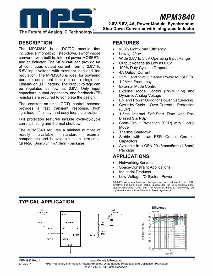
DESCRIPTION The MPM3840 is a DC/DC module that includes a monolithic, step-down, switch-mode converter with built-in, internal power MOSFETs and an inductor. The MPM3840 can provide 4A of continuous output current from a 2.8V to 5.5V input voltage with excellent load and line regulation. The MPM3840 is ideal for powering portable equipment that run on a single-cell Lithium-ion (Li+) battery. The output voltage can be regulated as low as 0.6V. Only input capacitors, output capacitors, and feedback (FB) resistors are required to complete the design.
The constant-on-time (COT) control scheme provides a fast transient response, high light-load efficiency, and easy loop stabilization.
Full protection features include cycle-by-cycle current limiting and thermal shutdown.
The MPM3840 requires a minimal number of readily available, standard, external components and is available in an ultra-small QFN-20 (3mmx5mmx1.6mm) package.
FEATURES >80% Light-Load Efficiency Low IQ: 40μA Wide 2.8V to 5.5V Operating Input Range Output Voltage as Low as 0.6V 100% Duty Cycle in Dropout 4A Output Current 25mΩ and 12mΩ Internal Power MOSFETs 1.2MHz Frequency External Mode Control External Mode Control (PWM.PFM) and
Dynamic Analog Voltage EN and Power Good for Power Sequencing Cycle-by-Cycle Over-Current Protection
(OCP) 1.5ms Internal Soft-Start Time with Pre-
Biased Start-Up Short-Circuit Protection (SCP) with Hiccup
Mode Thermal Shutdown Stable with Low ESR Output Ceramic
Capacitors Available in a QFN-20 (3mmx5mmx1.6mm)
Package
APPLICATIONS Networking/Servers Space-Constraint Applications Industrial Products Low-Voltage I/O System Power All MPS parts are lead-free, halogen-free, and adhere to the RoHS directive. For MPS green status, please visit the MPS website under Quality Assurance. “MPS” and “The Future of Analog IC Technology” are registered trademarks of Monolithic Power Systems, Inc.
TYPICAL APPLICATION
IOUT (A)
EfficiencyVIN=5V
0
10
20
30
40
50
60
70
80
90
100
0.001 0.01 0.1 1 10
Vo=1V@PWM
Vo=1.2V@PWM
Vo=1.5V@PWM
Vo=1.8V@PWM
Vo=1V@PFM
Vo=1.2V@PFM
Vo=1.5V@PFM
Vo=1.8V@PFM
Vo=2.5V@PWM
Vo=3.3V@PWM
Vo=2.5V@PFM
Vo=3.3V@PFM
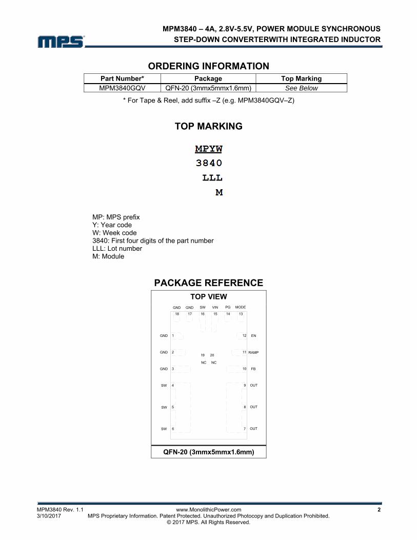
MPM3840 – 4A, 2.8V-5.5V, POWER MODULE SYNCHRONOUS
STEP-DOWN CONVERTERWITH INTEGRATED INDUCTOR
MPM3840 Rev. 1.1 www.MonolithicPower.com 2 3/10/2017 MPS Proprietary Information. Patent Protected. Unauthorized Photocopy and Duplication Prohibited. © 2017 MPS. All Rights Reserved.
ORDERING INFORMATION Part Number* Package Top Marking
MPM3840GQV QFN-20 (3mmx5mmx1.6mm) See Below
* For Tape & Reel, add suffix –Z (e.g. MPM3840GQV–Z)
TOP MARKING
MP: MPS prefix Y: Year code W: Week code 3840: First four digits of the part number LLL: Lot number M: Module
PACKAGE REFERENCE TOP VIEW
1
SW
12
6
PGVIN
SW
GND
SW
RAMP
SW
OUT
OUT
OUT
EN
FB
7
13
MODEGND
2
3
4
5
11
10
9
8
1415161718
GND
GND
GND
NC NC
19 20
QFN-20 (3mmx5mmx1.6mm)
MPM3840 – 4A, 2.8V-5.5V, POWER MODULE SYNCHRONOUS
STEP-DOWN CONVERTERWITH INTEGRATED INDUCTOR
MPM3840 Rev. 1.1 www.MonolithicPower.com 3 3/10/2017 MPS Proprietary Information. Patent Protected. Unauthorized Photocopy and Duplication Prohibited. © 2017 MPS. All Rights Reserved.
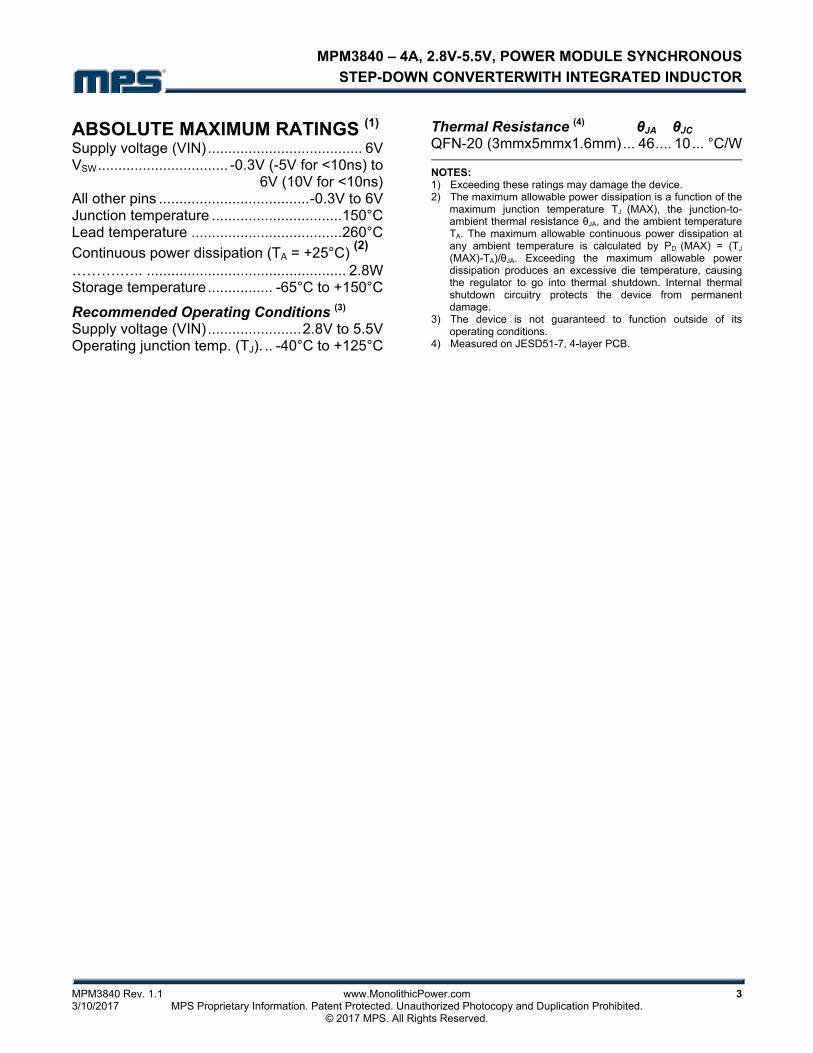
ABSOLUTE MAXIMUM RATINGS (1) Supply voltage (VIN) ...................................... 6V VSW ................................ -0.3V (-5V for <10ns) to
6V (10V for <10ns) All other pins ..................................... -0.3V to 6V Junction temperature ................................ 150°C Lead temperature ..................................... 260°C
Continuous power dissipation (TA = +25°C) (2)
……….….. ................................................. 2.8W Storage temperature ................ -65°C to +150°C
Recommended Operating Conditions (3) Supply voltage (VIN) ....................... 2.8V to 5.5V Operating junction temp. (TJ). .. -40°C to +125°C
Thermal Resistance (4) θJA θJC QFN-20 (3mmx5mmx1.6mm) ... 46 .... 10 ... °C/W
NOTES: 1) Exceeding these ratings may damage the device. 2) The maximum allowable power dissipation is a function of the
maximum junction temperature TJ (MAX), the junction-to-ambient thermal resistance θJA, and the ambient temperature TA. The maximum allowable continuous power dissipation at any ambient temperature is calculated by PD (MAX) = (TJ
(MAX)-TA)/θJA. Exceeding the maximum allowable power dissipation produces an excessive die temperature, causing the regulator to go into thermal shutdown. Internal thermal shutdown circuitry protects the device from permanent damage.
3) The device is not guaranteed to function outside of its operating conditions.
4) Measured on JESD51-7, 4-layer PCB.
MPM3840 – 4A, 2.8V-5.5V, POWER MODULE SYNCHRONOUS
STEP-DOWN CONVERTERWITH INTEGRATED INDUCTOR
MPM3840 Rev. 1.1 www.MonolithicPower.com 4 3/10/2017 MPS Proprietary Information. Patent Protected. Unauthorized Photocopy and Duplication Prohibited. © 2017 MPS. All Rights Reserved.
ELECTRICAL CHARACTERISTICS VIN = 3.6V, VOUT = 1.2V, TJ = -40°C to +125°C, typical value is tested at TJ = +25°C. The limit over temperature is guaranteed by characterization, unless otherwise noted.
Parameter Symbol Condition Min Typ Max Units
Feedback voltage VFB 2.8V ≤ VIN ≤ 5.5V 0.594 0.600 0.606 V
Feedback current IFB VFB = 0.65V 50 nA
P-FET switch on resistance RDSON P 25 mΩ
N-FET switch on resistance RDSON N 12 mΩ
Dropout resistance RDR 100% on duty 47 mΩ
Switch leakage TJ = 25°C 0 1 μA
P-FET peak current limit 4.5 5.5 6.5 A
N-FET valley current limit 4 A
On time TJ = 25°C 216
270 324
ns TJ = -40°C to 85°C 202 338
Switching frequency fs VOUT = 1.2V 1200 kHz
Minimum off time TMIN-OFF 60 ns
Minimum on time(5) TMIN-On 50 ns
Soft-start time TSS-ON 1.5 ms
PG UV threshold rising PGTH_Hi 0.9 VFB
PG UV threshold falling PGTH_Lo 0.85 VFB
PG OV threshold rising PGTH_Hi 1.15 VFB
PG OV threshold falling PGTH_Lo 1.1 VFB
Power good delay 140 μs
Power good sink current capability VPG LO Sink 1mA 0.4 V
Power good logic-high voltage VPG HI VIN = 5V, VFB = 0.6V 4.9 V
Power good internal pull-up resistor RPG 500 kΩ
Under-voltage lockout threshold rising 2.4 2.55 2.7 V
Under-voltage lockout threshold hysteresis
300 mV
EN input logic-low voltage 0.4 V
EN input logic-high voltage 1.2 V
EN input current VEN = 2V 2 μA
VEN = 0V 0 μA
Supply current (shutdown) VEN = 0V, TJ = 25°C 0.1 1 μA
Supply current (quiescent) VIN = 3.6V, VEN = 2V, VFB = 0.65V, TJ = 25°C
40 60 μA
Thermal shutdown(5) 150 °C
Thermal hysteresis(5) 20 °C
Inductor L value 0.47 μH
Inductor DC resistance 22 mΩ
NOTE: 5) Guaranteed by design.
MPM3840 – 4A, 2.8V-5.5V, POWER MODULE SYNCHRONOUS
STEP-DOWN CONVERTERWITH INTEGRATED INDUCTOR
MPM3840 Rev. 1.1 www.MonolithicPower.com 5 3/10/2017 MPS Proprietary Information. Patent Protected. Unauthorized Photocopy and Duplication Prohibited. © 2017 MPS. All Rights Reserved.
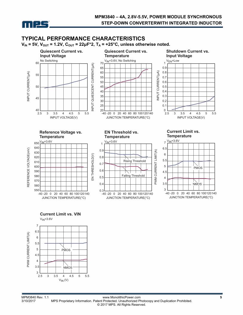
TYPICAL PERFORMANCE CHARACTERISTICS VIN = 5V, VOUT = 1.2V, COUT = 22μF*2, TA = +25°C, unless otherwise noted.
EN
TH
RE
SH
OLD
(V)
RE
FE
RE
NC
E V
OLT
AG
E(m
V)
Quiescent Current vs. TemperatureVIN=3.6V, No Switching
Shutdown Current vs. Input VoltageVEN=Low
EN Threshold vs. TemperatureVIN=3.6V
Reference Voltage vs. TemperatureVIN=3.6V
Current Limit vs. VINVIN=3.6V
Current Limit vs. TemperatureVIN=3.6V
INPUT VOLTAGE(V)
PW
M C
UR
RE
NT
LIM
IT(A
)
VIN (V)
PW
M C
UR
RE
NT
LIM
IT(A
)
INPUT VOLTAGE(V)
Quiescent Current vs. Input VoltageNo Switching
40
45
50
55
60
2.5 3 3.5 4 4.5 5 5.520
25
30
35
40
45
50
55
60
65
70
-40 -20 0 20 40 60 80 100120140 2.5 3 3.5 4 4.5 5 5.5
550
560
570
580
590
600
610
620
630
640
650
-40 -20 0 20 40 60 80 1001201400.3
0.4
0.5
0.6
0.7
0.8
0.9
1
-40 -20 0 20 40 60 80 100120140
Falling Threshold
Rising Threshold
3
3.5
4
4.5
5
5.5
6
6.5
7
-40 -20 0 20 40 60 80 100120140
NMOS
PMOS
3
3.5
4
4.5
5
5.5
6
6.5
7
2.5 3 3.5 4 4.5 5 5.5
NMOS
PMOS
0
0.1
0.2
0.3
0.4
0.5
0.6
0.7
0.8
0.9
1
MPM3840 – 4A, 2.8V-5.5V, POWER MODULE SYNCHRONOUS
STEP-DOWN CONVERTERWITH INTEGRATED INDUCTOR
MPM3840 Rev. 1.1 www.MonolithicPower.com 6 3/10/2017 MPS Proprietary Information. Patent Protected. Unauthorized Photocopy and Duplication Prohibited. © 2017 MPS. All Rights Reserved.
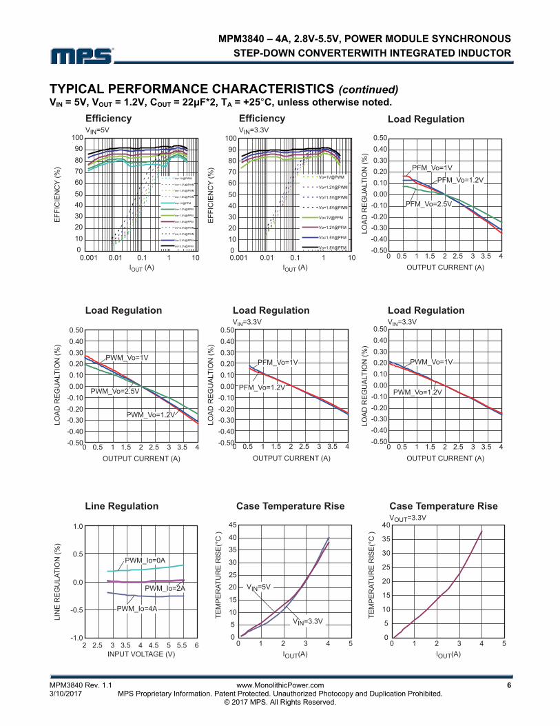
TYPICAL PERFORMANCE CHARACTERISTICS (continued) VIN = 5V, VOUT = 1.2V, COUT = 22μF*2, TA = +25°C, unless otherwise noted.
IOUT (A)
EfficiencyVIN=3.3V
IOUT (A)
EfficiencyVIN=5V
0
10
20
30
40
50
60
70
80
90
100
0.001 0.01 0.1 1 10
Vo=1V@PWM
Vo=1.2V@PWM
Vo=1.5V@PWM
Vo=1.8V@PWM
Vo=1V@PFM
Vo=1.2V@PFM
Vo=1.5V@PFM
Vo=1.8V@PFM
Vo=2.5V@PWM
Vo=3.3V@PWM
Vo=2.5V@PFM
Vo=3.3V@PFM
0
10
20
30
40
50
60
70
80
90
100
0.001 0.01 0.1 1 10
Vo=1V@PWM
Vo=1.2V@PWM
Vo=1.5V@PWM
Vo=1.8V@PWM
Vo=1V@PFM
Vo=1.2V@PFM
Vo=1.5V@PFM
Vo=1.8V@PFM
OUTPUT CURRENT (A)
OUTPUT CURRENT (A)
Load Regulation Load RegulationVIN=3.3V
Load Regulation
Line Regulation
Load RegulationVIN=3.3V
OUTPUT CURRENT (A)
INPUT VOLTAGE (V)
OUTPUT CURRENT (A)
-1.0
-0.5
0.0
0.5
1.0
2 2.5 3 3.5 4 4.5 5 5.5 6
0 0.5 1 1.5 2 2.5 3 3.5 4
0 0.5 1 1.5 2 2.5 3 3.5 4 0 0.5 1 1.5 2 2.5 3 3.5 4 0 0.5 1 1.5 2 2.5 3 3.5 4
PWM_Io=2A
PWM_Io=0A
PWM_Io=4A
-0.50
-0.40
-0.30
-0.20
-0.10
0.00
0.10
0.20
0.30
0.40
0.50
-0.50
-0.40
-0.30
-0.20
-0.10
0.00
0.10
0.20
0.30
0.40
0.50
-0.50
-0.40
-0.30
-0.20
-0.10
0.00
0.10
0.20
0.30
0.40
0.50
-0.50
-0.40
-0.30
-0.20
-0.10
0.00
0.10
0.20
0.30
0.40
0.50
PFM_Vo=2.5V
PFM_Vo=1V
PFM_Vo=1.2V
PWM_Vo=2.5V
PWM_Vo=1V
PWM_Vo=1.2V
PFM_Vo=1V
PFM_Vo=1.2V
PWM_Vo=1V
PWM_Vo=1.2V
Case Temperature Rise
IOUT(A)
Case Temperature RiseVOUT=3.3V
IOUT(A)
0
5
10
15
20
25
30
35
40
45
0 1 2 3 4 5
VIN=3.3V
VIN=5V
0
5
10
15
20
25
30
35
40
0 1 2 3 4 5
MPM3840 – 4A, 2.8V-5.5V, POWER MODULE SYNCHRONOUS
STEP-DOWN CONVERTERWITH INTEGRATED INDUCTOR
MPM3840 Rev. 1.1 www.MonolithicPower.com 7 3/10/2017 MPS Proprietary Information. Patent Protected. Unauthorized Photocopy and Duplication Prohibited. © 2017 MPS. All Rights Reserved.
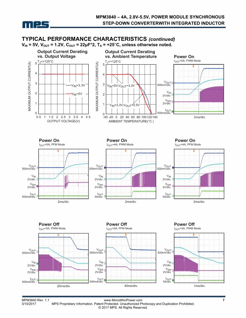
TYPICAL PERFORMANCE CHARACTERISTICS (continued) VIN = 5V, VOUT = 1.2V, COUT = 22μF*2, TA = +25°C, unless otherwise noted.
Power OnIOUT=0A, PWM Mode
Power OnIOUT=0A, PFM Mode
Power OnIOUT=4A, PWM Mode
Power OnIOUT=4A, PFM Mode
VIN2V/div.
VSW2V/div.
VOUT500mV/div.
IOUT500mA/div.
VIN2V/div.
VSW2V/div.
VOUT500mV/div.
IOUT500mA/div.
VIN2V/div.
VSW2V/div.
VOUT500mV/div.
IOUT5A/div.
VIN2V/div.
VSW2V/div.
VOUT500mV/div.
IOUT5A/div.
MA
XIM
UM
OU
TP
UT
CU
RR
EN
T(A
)
MA
XIM
UM
OU
TP
UT
CU
RR
EN
T(A
)
OUTPUT VOLTAGE(V)
0
1
2
3
4
5
0.5 1 1.5 2 2.5 3 3.5 4 4.5
VIN=3.3V
VIN=5V
0
1
2
3
4
5
-40 -20 0 20 40 60 80 100120140
VIN=3.3V,VOUT=2.5V
VIN=5V,VOUT=3.3V
VIN2V/div.
VSW2V/div.
VOUT500mV/div.
IOUT500mA/div.
Power OffIOUT=0A, PWM Mode
VIN2V/div.
VSW2V/div.
VOUT500mV/div.
IOUT500mA/div.
VIN2V/div.
VSW2V/div.
VOUT500mV/div.
IOUT5A/div.
Power OffIOUT=0A, PFM Mode
Power OffIOUT=4A, PWM Mode
MPM3840 – 4A, 2.8V-5.5V, POWER MODULE SYNCHRONOUS
STEP-DOWN CONVERTERWITH INTEGRATED INDUCTOR
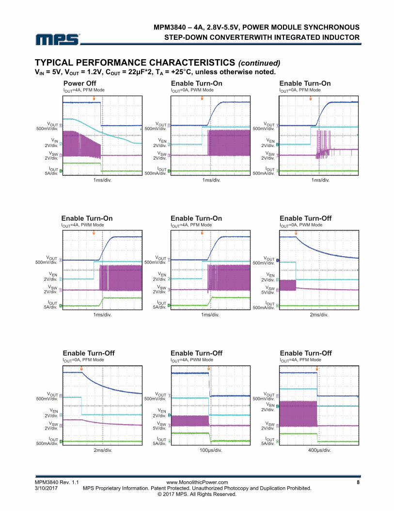
MPM3840 Rev. 1.1 www.MonolithicPower.com 8 3/10/2017 MPS Proprietary Information. Patent Protected. Unauthorized Photocopy and Duplication Prohibited. © 2017 MPS. All Rights Reserved.
TYPICAL PERFORMANCE CHARACTERISTICS (continued) VIN = 5V, VOUT = 1.2V, COUT = 22μF*2, TA = +25°C, unless otherwise noted.
Enable Turn-OnIOUT=0A, PWM Mode
Enable Turn-OnIOUT=4A, PWM Mode
Enable Turn-OnIOUT=4A, PFM Mode
Enable Turn-OffIOUT=0A, PWM Mode
Enable Turn-OnIOUT=0A, PFM Mode
VIN2V/div.
VSW2V/div.
VOUT500mV/div.
IOUT5A/div.
VEN2V/div.
VSW2V/div.
VOUT500mV/div.
IOUT500mA/div.
VEN2V/div.
VSW2V/div.
VOUT500mV/div.
IOUT5A/div.
VEN2V/div.
VSW2V/div.
VOUT500mV/div.
IOUT5A/div.
VEN2V/div.
VSW2V/div.
VOUT500mV/div.
IOUT500mA/div.
VEN2V/div.
VSW5V/div.
VOUT500mV/div.
IOUT500mA/div.
Power OffIOUT=4A, PFM Mode
Enable Turn-OffIOUT=0A, PFM Mode
Enable Turn-OffIOUT=4A, PWM Mode
Enable Turn-OffIOUT=4A, PFM Mode
VEN2V/div.
VSW2V/div.
VOUT500mV/div.
IOUT500mA/div.
VEN2V/div.
VSW5V/div.
VOUT500mV/div.
IOUT5A/div.
VEN2V/div.
VSW2V/div.
VOUT500mV/div.
IOUT5A/div.
MPM3840 – 4A, 2.8V-5.5V, POWER MODULE SYNCHRONOUS
STEP-DOWN CONVERTERWITH INTEGRATED INDUCTOR
MPM3840 Rev. 1.1 www.MonolithicPower.com 9 3/10/2017 MPS Proprietary Information. Patent Protected. Unauthorized Photocopy and Duplication Prohibited. © 2017 MPS. All Rights Reserved.
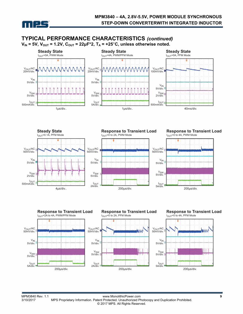
TYPICAL PERFORMANCE CHARACTERISTICS (continued) VIN = 5V, VOUT = 1.2V, COUT = 22μF*2, TA = +25°C, unless otherwise noted.
VIN5V/div.
VSW5V/div.
VOUT/AC20mV/div.
IOUT500mA/div.
VIN5V/div.
VSW2V/div.
VOUT/AC50mV/div.
IOUT500mA/div.
VIN5V/div.
VSW5V/div.
VOUT/AC50mV/div.
IOUT2A/div.
VIN5V/div.
VSW5V/div.
VOUT/AC50mV/div.
IOUT5A/div.
VIN5V/div.
VSW5V/div.
VOUT/AC20mV/div.
IOUT5A/div.
VIN5V/div.
VSW2V/div.
VOUT/AC100mV/div.
IOUT500mA/div.
Steady StateIOUT=0A, PWM Mode
Steady StateIOUT=0A, PFM Mode
Steady StateIOUT=4A, PWM/PFM Mode
Steady StateIOUT=0.1A, PFM Mode
Response to Transient LoadIOUT=0 to 2A, PWM Mode
Response to Transient LoadIOUT=0 to 4A, PWM Mode
VIN5V/div.
VSW5V/div.
VOUT/AC50mV/div.
IOUT5A/div.
VIN5V/div.
VSW5V/div.
VOUT/AC50mV/div.
IOUT5A/div.
VIN5V/div.
VSW5V/div.
VOUT/AC50mV/div.
IOUT2A/div.
Response to Transient LoadIOUT=2A to 4A, PWM/PFM Mode
Response to Transient LoadIOUT=0 to 2A, PFM Mode
Response to Transient LoadIOUT=0 to 4A, PFM Mode
MPM3840 – 4A, 2.8V-5.5V, POWER MODULE SYNCHRONOUS
STEP-DOWN CONVERTERWITH INTEGRATED INDUCTOR
MPM3840 Rev. 1.1 www.MonolithicPower.com 10 3/10/2017 MPS Proprietary Information. Patent Protected. Unauthorized Photocopy and Duplication Prohibited. © 2017 MPS. All Rights Reserved.
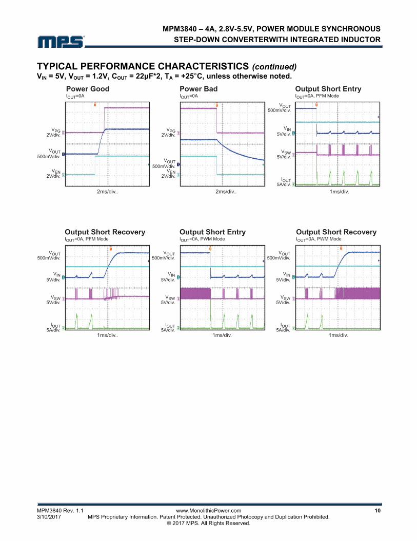
TYPICAL PERFORMANCE CHARACTERISTICS (continued) VIN = 5V, VOUT = 1.2V, COUT = 22μF*2, TA = +25°C, unless otherwise noted.
VOUT500mV/div.
VEN2V/div.
VPG2V/div.
VOUT500mV/div.
VEN2V/div.
VPG2V/div.
VIN5V/div.
VSW5V/div.
VOUT500mV/div.
IOUT5A/div.
VIN5V/div.
VSW5V/div.
VOUT500mV/div.
IOUT5A/div.
VIN5V/div.
VSW5V/div.
VOUT500mV/div.
IOUT5A/div.
VIN5V/div.
VSW5V/div.
VOUT500mV/div.
IOUT5A/div.
Power GoodIOUT=0A
Output Short EntryIOUT=0A, PFM Mode
Power BadIOUT=0A
Output Short RecoveryIOUT=0A, PFM Mode
Output Short EntryIOUT=0A, PWM Mode
Output Short RecoveryIOUT=0A, PWM Mode
MPM3840 – 4A, 2.8V-5.5V, POWER MODULE SYNCHRONOUS
STEP-DOWN CONVERTERWITH INTEGRATED INDUCTOR
MPM3840 Rev. 1.1 www.MonolithicPower.com 11 3/10/2017 MPS Proprietary Information. Patent Protected. Unauthorized Photocopy and Duplication Prohibited. © 2017 MPS. All Rights Reserved.
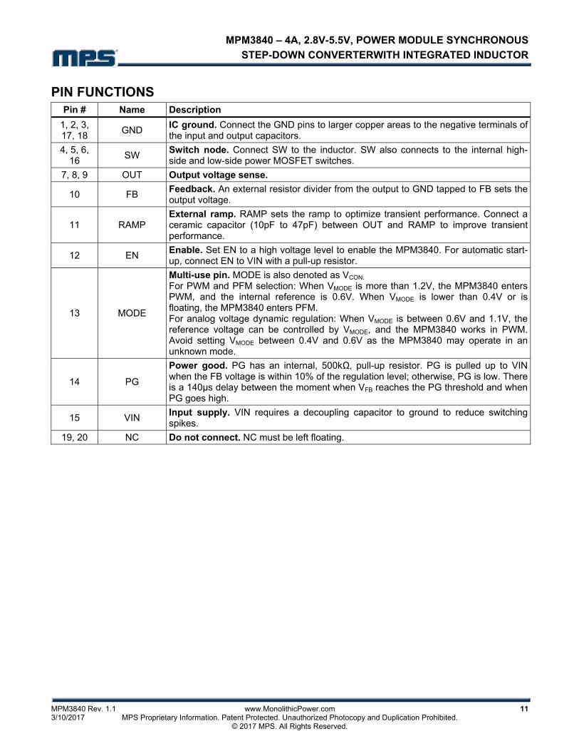
PIN FUNCTIONS Pin # Name Description
1, 2, 3, 17, 18
GND IC ground. Connect the GND pins to larger copper areas to the negative terminals of the input and output capacitors.
4, 5, 6, 16
SW Switch node. Connect SW to the inductor. SW also connects to the internal high-side and low-side power MOSFET switches.
7, 8, 9 OUT Output voltage sense.
10 FB Feedback. An external resistor divider from the output to GND tapped to FB sets the output voltage.
11 RAMP External ramp. RAMP sets the ramp to optimize transient performance. Connect a ceramic capacitor (10pF to 47pF) between OUT and RAMP to improve transient performance.
12 EN Enable. Set EN to a high voltage level to enable the MPM3840. For automatic start-up, connect EN to VIN with a pull-up resistor.
13 MODE
Multi-use pin. MODE is also denoted as VCON.
For PWM and PFM selection: When VMODE is more than 1.2V, the MPM3840 enters PWM, and the internal reference is 0.6V. When VMODE is lower than 0.4V or is floating, the MPM3840 enters PFM. For analog voltage dynamic regulation: When VMODE is between 0.6V and 1.1V, the reference voltage can be controlled by VMODE, and the MPM3840 works in PWM. Avoid setting VMODE between 0.4V and 0.6V as the MPM3840 may operate in an unknown mode.
14 PG
Power good. PG has an internal, 500kΩ, pull-up resistor. PG is pulled up to VIN when the FB voltage is within 10% of the regulation level; otherwise, PG is low. There is a 140μs delay between the moment when VFB reaches the PG threshold and when PG goes high.
15 VIN Input supply. VIN requires a decoupling capacitor to ground to reduce switchingspikes.
19, 20 NC Do not connect. NC must be left floating.
MPM3840 – 4A, 2.8V-5.5V, POWER MODULE SYNCHRONOUS
STEP-DOWN CONVERTERWITH INTEGRATED INDUCTOR
MPM3840 Rev. 1.1 www.MonolithicPower.com 12 3/10/2017 MPS Proprietary Information. Patent Protected. Unauthorized Photocopy and Duplication Prohibited. © 2017 MPS. All Rights Reserved.
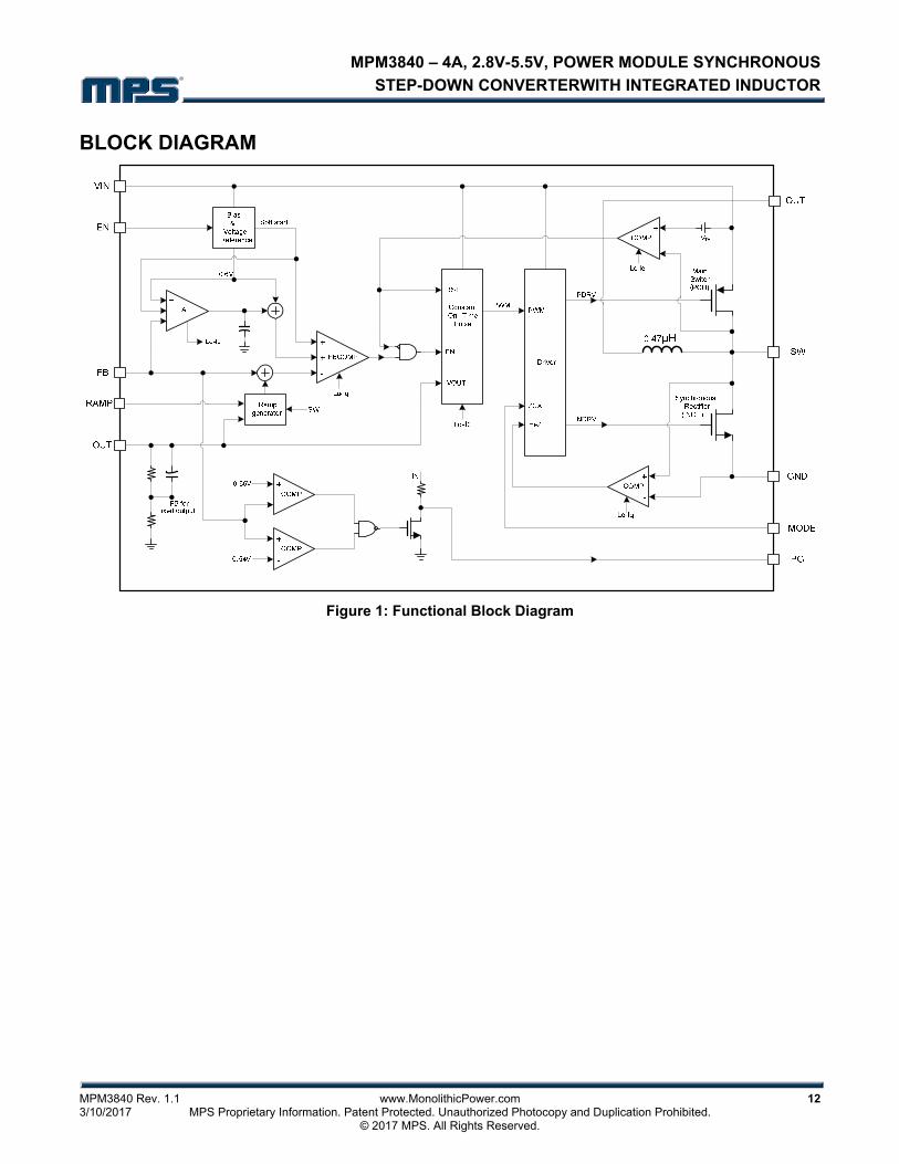
BLOCK DIAGRAM
Figure 1: Functional Block Diagram
MPM3840 – 4A, 2.8V-5.5V, POWER MODULE SYNCHRONOUS
STEP-DOWN CONVERTERWITH INTEGRATED INDUCTOR
MPM3840 Rev. 1.1 www.MonolithicPower.com 13 3/10/2017 MPS Proprietary Information. Patent Protected. Unauthorized Photocopy and Duplication Prohibited. © 2017 MPS. All Rights Reserved.
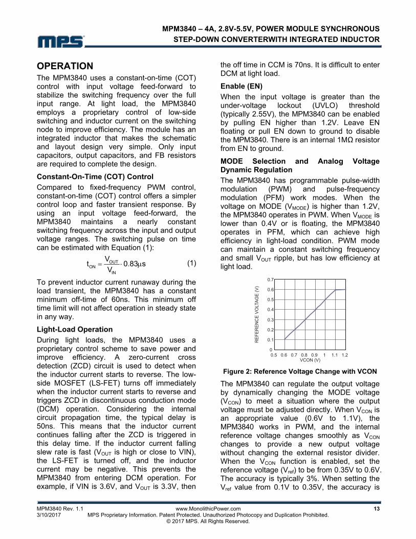
OPERATION The MPM3840 uses a constant-on-time (COT) control with input voltage feed-forward to stabilize the switching frequency over the full input range. At light load, the MPM3840 employs a proprietary control of low-side switching and inductor current on the switching node to improve efficiency. The module has an integrated inductor that makes the schematic and layout design very simple. Only input capacitors, output capacitors, and FB resistors are required to complete the design.
Constant-On-Time (COT) Control
Compared to fixed-frequency PWM control, constant-on-time (COT) control offers a simpler control loop and faster transient response. By using an input voltage feed-forward, the MPM3840 maintains a nearly constant switching frequency across the input and output voltage ranges. The switching pulse on time can be estimated with Equation (1):
OUTON
IN
Vt 0.83 s
V (1)
To prevent inductor current runaway during the load transient, the MPM3840 has a constant minimum off-time of 60ns. This minimum off time limit will not affect operation in steady state in any way.
Light-Load Operation During light loads, the MPM3840 uses a proprietary control scheme to save power and improve efficiency. A zero-current cross detection (ZCD) circuit is used to detect when the inductor current starts to reverse. The low-side MOSFET (LS-FET) turns off immediately when the inductor current starts to reverse and triggers ZCD in discontinuous conduction mode (DCM) operation. Considering the internal circuit propagation time, the typical delay is 50ns. This means that the inductor current continues falling after the ZCD is triggered in this delay time. If the inductor current falling slew rate is fast (VOUT is high or close to VIN), the LS-FET is turned off, and the inductor current may be negative. This prevents the MPM3840 from entering DCM operation. For example, if VIN is 3.6V, and VOUT is 3.3V, then
the off time in CCM is 70ns. It is difficult to enter DCM at light load.
Enable (EN) When the input voltage is greater than the under-voltage lockout (UVLO) threshold (typically 2.55V), the MPM3840 can be enabled by pulling EN higher than 1.2V. Leave EN floating or pull EN down to ground to disable the MPM3840. There is an internal 1MΩ resistor from EN to ground.
MODE Selection and Analog Voltage Dynamic Regulation
The MPM3840 has programmable pulse-width modulation (PWM) and pulse-frequency modulation (PFM) work modes. When the voltage on MODE (VMODE) is higher than 1.2V, the MPM3840 operates in PWM. When VMODE is lower than 0.4V or is floating, the MPM3840 operates in PFM, which can achieve high efficiency in light-load condition. PWM mode can maintain a constant switching frequency and small VOUT ripple, but has low efficiency at light load.
RE
FE
RE
NC
E V
OLT
AG
E (
V)
VCON (V)
0
0.1
0.2
0.3
0.4
0.5
0.6
0.7
0.5 0.6 0.7 0.8 0.9 1 1.1 1.2
Figure 2: Reference Voltage Change with VCON
The MPM3840 can regulate the output voltage by dynamically changing the MODE voltage (VCON) to meet a situation where the output voltage must be adjusted directly. When VCON is an appropriate value (0.6V to 1.1V), the MPM3840 works in PWM, and the internal reference voltage changes smoothly as VCON changes to provide a new output voltage without changing the external resistor divider. When the VCON function is enabled, set the reference voltage (Vref) to be from 0.35V to 0.6V. The accuracy is typically 3%. When setting the Vref value from 0.1V to 0.35V, the accuracy is
MPM3840 – 4A, 2.8V-5.5V, POWER MODULE SYNCHRONOUS
STEP-DOWN CONVERTERWITH INTEGRATED INDUCTOR
MPM3840 Rev. 1.1 www.MonolithicPower.com 14 3/10/2017 MPS Proprietary Information. Patent Protected. Unauthorized Photocopy and Duplication Prohibited. © 2017 MPS. All Rights Reserved.
typically 10%. The detailed VRef curve is shown in Figure 2. Calculate Vref with Equation (2):
Ref(V)=0.985 VCON(V)-0.486 (2)
Soft Start (SS)
The MPM3840 has a built-in soft start (SS) that ramps up the output voltage at a constant slew rate to avoid overshooting at start-up. The soft-start time is about 1.5ms, typically.
Pre-Bias Start-Up
The MPM3840 can start up with a pre-biased output voltage. If the internal SS voltage is lower than the FB voltage, the HS-FET and LS-FET remain off until the SS voltage crosses the FB voltage.
Power Good (PG) Indicator
The MPM3840 has an open drain with a 500kΩ pull-up resistor as a power good (PG) indicator.
PG is pulled up to VIN when the FB voltage is within 10% of the regulation level; otherwise, PG is low. There is a 140μs delay between the moment when VFB reaches the PG threshold and when PG goes high. The MOSFET has a maximum RDS(ON) of 100Ω.
Current Limit
The MPM3840 has a 5.5A current limit for the HS-FET. When the HS-FET reaches its current limit, the MPM3840 enters hiccup mode until the current drops to prevent the inductor current from rising and damaging the components.
Short Circuit and Recovery
The MPM3840 enters short-circuit protection (SCP) mode when it reaches the current limit and attempts to recover with hiccup mode. The MPM3840 disables the output power stage, discharges the soft-start capacitor, and attempts to soft start. If the short-circuit condition remains after the soft start ends, the MPM3840 repeats this operation until the short circuit is removed and the output rises back to regulation levels.
MPM3840 – 4A, 2.8V-5.5V, POWER MODULE SYNCHRONOUS
STEP-DOWN CONVERTERWITH INTEGRATED INDUCTOR
MPM3840 Rev. 1.1 www.MonolithicPower.com 15 3/10/2017 MPS Proprietary Information. Patent Protected. Unauthorized Photocopy and Duplication Prohibited. © 2017 MPS. All Rights Reserved.
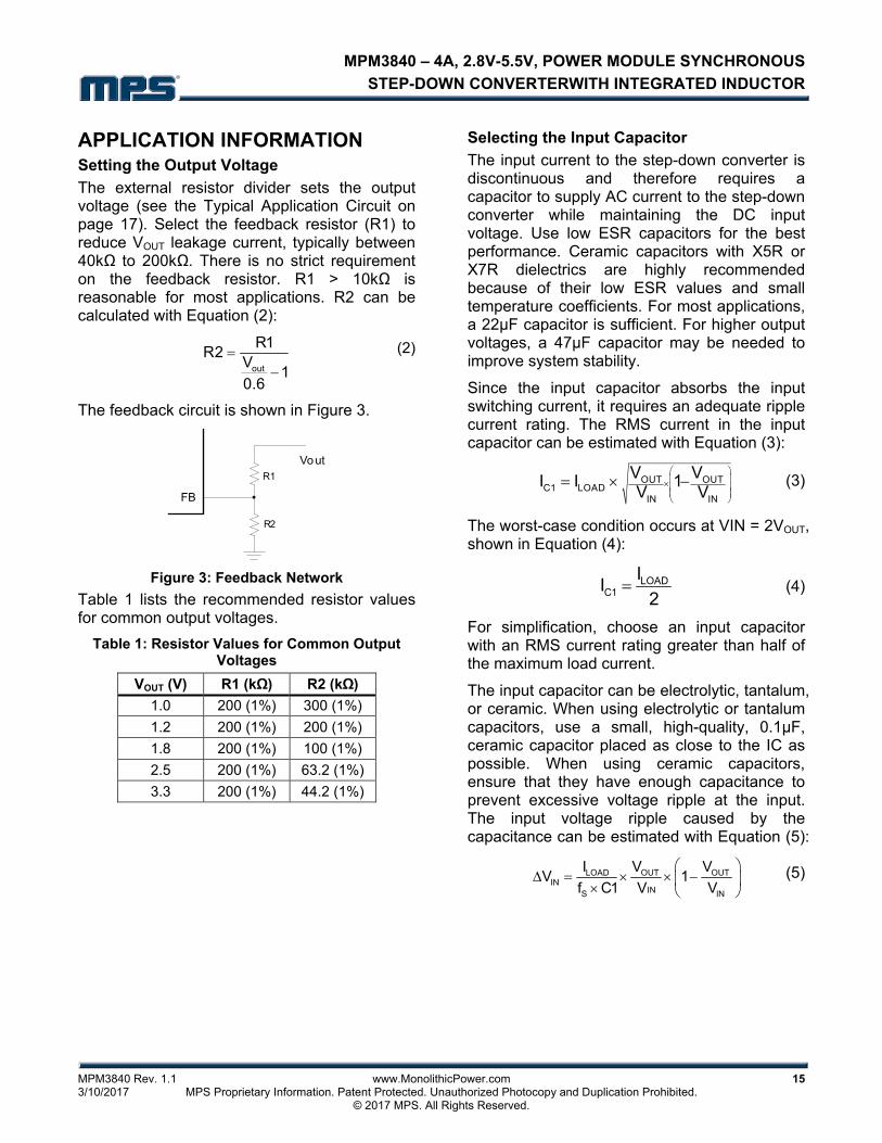
APPLICATION INFORMATION Setting the Output Voltage
The external resistor divider sets the output voltage (see the Typical Application Circuit on page 17). Select the feedback resistor (R1) to reduce VOUT leakage current, typically between 40kΩ to 200kΩ. There is no strict requirement on the feedback resistor. R1 > 10kΩ is reasonable for most applications. R2 can be calculated with Equation (2):
out
R1R2
V1
0.6
(2)
The feedback circuit is shown in Figure 3.
R1
R2
Vout
FB
Figure 3: Feedback Network
Table 1 lists the recommended resistor values for common output voltages.
Table 1: Resistor Values for Common Output Voltages
VOUT (V) R1 (kΩ) R2 (kΩ)
1.0 200 (1%) 300 (1%)
1.2 200 (1%) 200 (1%)
1.8 200 (1%) 100 (1%)
2.5 200 (1%) 63.2 (1%)
3.3 200 (1%) 44.2 (1%)
Selecting the Input Capacitor The input current to the step-down converter is discontinuous and therefore requires a capacitor to supply AC current to the step-down converter while maintaining the DC input voltage. Use low ESR capacitors for the best performance. Ceramic capacitors with X5R or X7R dielectrics are highly recommended because of their low ESR values and small temperature coefficients. For most applications, a 22µF capacitor is sufficient. For higher output voltages, a 47µF capacitor may be needed to improve system stability.
Since the input capacitor absorbs the input switching current, it requires an adequate ripple current rating. The RMS current in the input capacitor can be estimated with Equation (3):
OUT OUTC1 LOAD
IN IN
V VI I 1V V
(3)
The worst-case condition occurs at VIN = 2VOUT, shown in Equation (4):
LOADC1
II
2 (4)
For simplification, choose an input capacitor with an RMS current rating greater than half of the maximum load current.
The input capacitor can be electrolytic, tantalum, or ceramic. When using electrolytic or tantalum capacitors, use a small, high-quality, 0.1μF, ceramic capacitor placed as close to the IC as possible. When using ceramic capacitors, ensure that they have enough capacitance to prevent excessive voltage ripple at the input. The input voltage ripple caused by the capacitance can be estimated with Equation (5):
LOAD OUT OUTIN
INS IN
I V VV 1
f C1 V V
(5)
MPM3840 – 4A, 2.8V-5.5V, POWER MODULE SYNCHRONOUS
STEP-DOWN CONVERTERWITH INTEGRATED INDUCTOR
MPM3840 Rev. 1.1 www.MonolithicPower.com 16 3/10/2017 MPS Proprietary Information. Patent Protected. Unauthorized Photocopy and Duplication Prohibited. © 2017 MPS. All Rights Reserved.
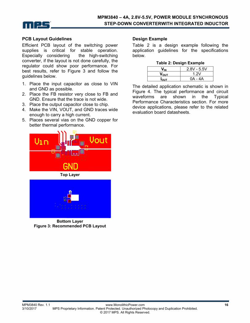
PCB Layout Guidelines
Efficient PCB layout of the switching power supplies is critical for stable operation. Especially considering the high-switching converter, if the layout is not done carefully, the regulator could show poor performance. For best results, refer to Figure 3 and follow the guidelines below.
1. Place the input capacitor as close to VIN and GND as possible.
2. Place the FB resistor very close to FB and GND. Ensure that the trace is not wide.
3. Place the output capacitor close to chip. 4. Make the VIN, VOUT, and GND traces wide
enough to carry a high current. 5. Places several vias on the GND copper for
better thermal performance.
Top Layer
Bottom Layer
Figure 3: Recommended PCB Layout
Design Example
Table 2 is a design example following the application guidelines for the specifications below.
Table 2: Design Example
VIN 2.8V - 5.5V VOUT 1.2V IOUT 0A - 4A
The detailed application schematic is shown in Figure 4. The typical performance and circuit waveforms are shown in the Typical Performance Characteristics section. For more device applications, please refer to the related evaluation board datasheets.
MPM3840 – 4A, 2.8V-5.5V, POWER MODULE SYNCHRONOUS
STEP-DOWN CONVERTERWITH INTEGRATED INDUCTOR
MPM3840 Rev. 1.1 www.MonolithicPower.com 17 3/10/2017 MPS Proprietary Information. Patent Protected. Unauthorized Photocopy and Duplication Prohibited. © 2017 MPS. All Rights Reserved.
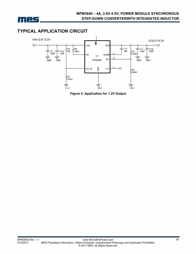
TYPICAL APPLICATION CIRCUIT
GN
DS
WS
WS
WS
W
Figure 4: Application for 1.2V Output
MPM3840 – 4A, 2.8V-5.5V, POWER MODULE SYNCHRONOUS
STEP-DOWN CONVERTERWITH INTEGRATED INDUCTOR
NOTICE: The information in this document is subject to change without notice. Please contact MPS for current specifications. Users should warrant and guarantee that third party Intellectual Property rights are not infringed upon when integrating MPS products into any application. MPS will not assume any legal responsibility for any said applications.
MPM3840 Rev. 1.1 www.MonolithicPower.com 18 3/10/2017 MPS Proprietary Information. Patent Protected. Unauthorized Photocopy and Duplication Prohibited. © 2017 MPS. All Rights Reserved.
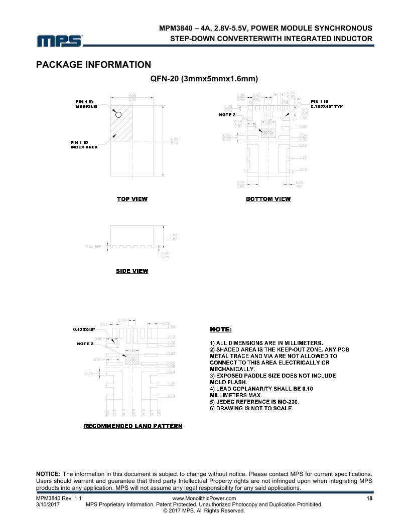
PACKAGE INFORMATION
QFN-20 (3mmx5mmx1.6mm)