Embed Size (px)
Citation preview
Page 1
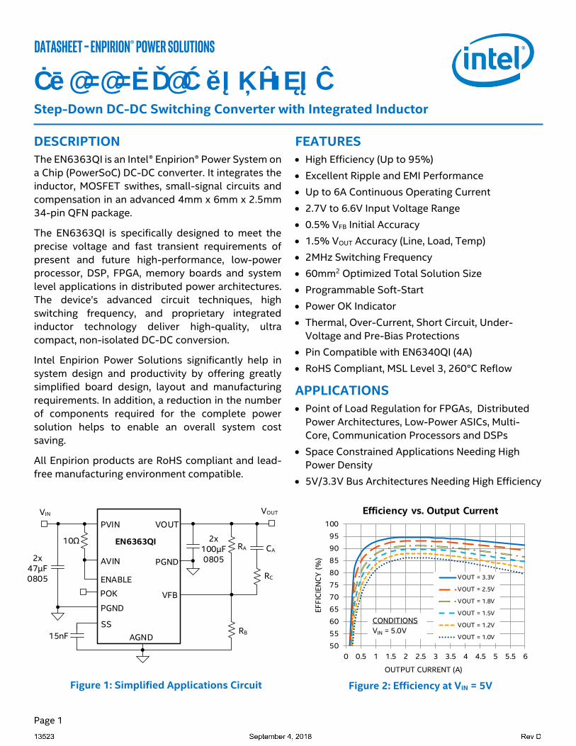
EN6363QI 6A PowerSoC Step-Down DC-DC Switching Converter with Integrated Inductor
DESCRIPTION
The EN6363QI is an Intel® Enpirion® Power System on
a Chip (PowerSoC) DC-DC converter. It integrates the
inductor, MOSFET swithes, small-signal circuits and
compensation in an advanced 4mm x 6mm x 2.5mm
34-pin QFN package.
The EN6363QI is specifically designed to meet the
precise voltage and fast transient requirements of
present and future high-performance, low-power
processor, DSP, FPGA, memory boards and system
level applications in distributed power architectures.
The device’s advanced circuit techniques, high
switching frequency, and proprietary integrated
inductor technology deliver high-quality, ultra
compact, non-isolated DC-DC conversion.
Intel Enpirion Power Solutions significantly help in
system design and productivity by offering greatly
simplified board design, layout and manufacturing
requirements. In addition, a reduction in the number
of components required for the complete power
solution helps to enable an overall system cost
saving.
All Enpirion products are RoHS compliant and lead-
free manufacturing environment compatible.
FEATURES
• High Efficiency (Up to 95%)
• Excellent Ripple and EMI Performance
• Up to 6A Continuous Operating Current
• 2.7V to 6.6V Input Voltage Range
• 0.5% VFB Initial Accuracy
• 1.5% VOUT Accuracy (Line, Load, Temp)
• 2MHz Switching Frequency
• 60mm2 Optimized Total Solution Size
• Programmable Soft-Start
• Power OK Indicator
• Thermal, Over-Current, Short Circuit, Under-
Voltage and Pre-Bias Protections
• Pin Compatible with EN6340QI (4A)
• RoHS Compliant, MSL Level 3, 260°C Reflow
APPLICATIONS
• Point of Load Regulation for FPGAs, Distributed
Power Architectures, Low-Power ASICs, Multi-
Core, Communication Processors and DSPs
• Space Constrained Applications Needing High
Power Density
• 5V/3.3V Bus Architectures Needing High Efficiency
Figure 1: Simplified Applications Circuit
Figure 2: Efficiency at VIN = 5V
DataSheeT – enpirion® power solutions
50
55
60
65
70
75
80
85
90
95
100
0 0.5 1 1.5 2 2.5 3 3.5 4 4.5 5 5.5 6
EF
FIC
IEN
CY
(%
)
OUTPUT CURRENT (A)
Efficiency vs. Output Current
VOUT = 3.3V
VOUT = 2.5V
VOUT = 1.8V
VOUT = 1.5V
VOUT = 1.2V
VOUT = 1.0V
CONDITIONS
VIN = 5.0V
VOUTVIN
2x47µF0805
VOUT
AVIN
AGND
SS
PVIN
ENABLE
PGND
PGND
EN6363QI
15nF
VFB
RA
RB
RC
CA
2x100µF0805
10Ω
POK
Datasheet | Intel® Enpirion® Power Solutions: EN6363QI
Page 2
ORDERING INFORMATION
Part Number Package Markings TJ Rating Package Description
EN6363QI EN6363QI -40°C to +125°C 34-pin (4mm x 6mm x 2.5mm) QFN
EVB-EN6363QI EN6363QI QFN Evaluation Board
Packing and Marking Information: https://www.altera.com/support/quality-and-reliability/packing.html
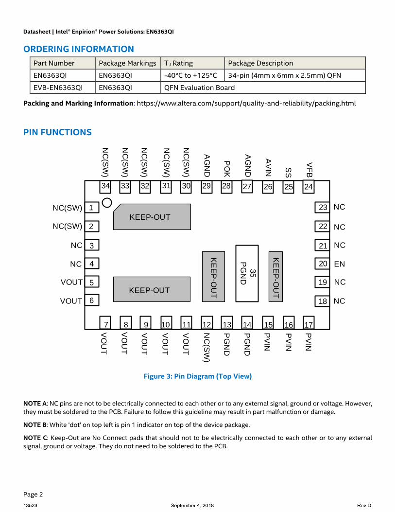
PIN FUNCTIONS
Figure 3: Pin Diagram (Top View)
NOTE A: NC pins are not to be electrically connected to each other or to any external signal, ground or voltage. However,
they must be soldered to the PCB. Failure to follow this guideline may result in part malfunction or damage.
NOTE B: White ‘dot’ on top left is pin 1 indicator on top of the device package.
NOTE C: Keep-Out are No Connect pads that should not to be electrically connected to each other or to any external
signal, ground or voltage. They do not need to be soldered to the PCB.
NC(SW)
NC
(SW
)
NC
(SW
)
NC
(SW
)
NC
(SW
)
NC
VO
UT
VO
UT
VO
UT
VO
UT
AV
IN
PO
K
AG
ND
35
PG
ND
1
2
3
4
7 8 9 10 11 12 13 14
2728293031323334N
C(S
W)
PG
ND
PG
ND
NC(SW)
VOUT 5
6VOUT
NC
15 16 17
NC
NC
23
22
21
20
NC
NC19
18 NC
EN
26 25 24
PV
IN
PV
IN
PV
IN
VO
UT
VF
B
SS
AG
ND
NC
(SW
)
KEEP-OUT
KE
EP
-OU
T
KE
EP
-OU
T
KEEP-OUT
Datasheet | Intel® Enpirion® Power Solutions: EN6363QI
Page 3
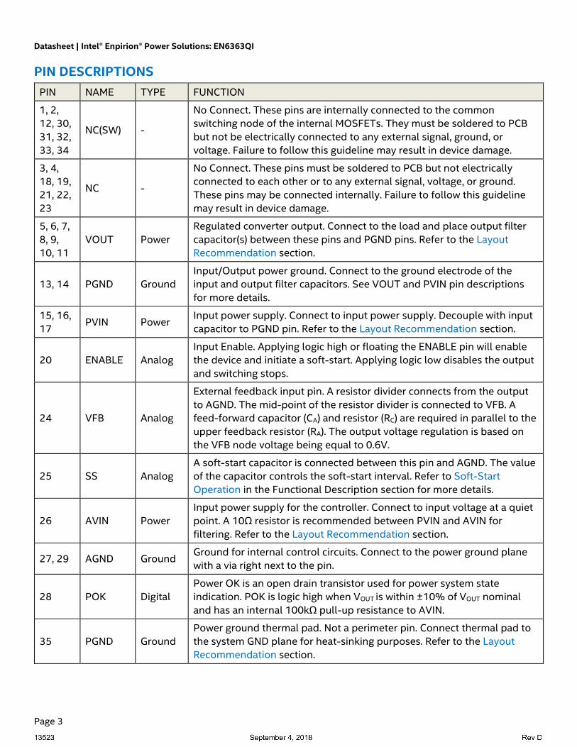
PIN DESCRIPTIONS
PIN NAME TYPE FUNCTION
1, 2,
12, 30,
31, 32,
33, 34
NC(SW) -
No Connect. These pins are internally connected to the common
switching node of the internal MOSFETs. They must be soldered to PCB
but not be electrically connected to any external signal, ground, or
voltage. Failure to follow this guideline may result in device damage.
3, 4,
18, 19,
21, 22,
23
NC -
No Connect. These pins must be soldered to PCB but not electrically
connected to each other or to any external signal, voltage, or ground.
These pins may be connected internally. Failure to follow this guideline
may result in device damage.
5, 6, 7,
8, 9,
10, 11
VOUT Power
Regulated converter output. Connect to the load and place output filter
capacitor(s) between these pins and PGND pins. Refer to the Layout
Recommendation section.
13, 14 PGND Ground
Input/Output power ground. Connect to the ground electrode of the
input and output filter capacitors. See VOUT and PVIN pin descriptions
for more details.
15, 16,
17 PVIN Power
Input power supply. Connect to input power supply. Decouple with input
capacitor to PGND pin. Refer to the Layout Recommendation section.
20 ENABLE Analog
Input Enable. Applying logic high or floating the ENABLE pin will enable
the device and initiate a soft-start. Applying logic low disables the output
and switching stops.
24 VFB Analog
External feedback input pin. A resistor divider connects from the output
to AGND. The mid-point of the resistor divider is connected to VFB. A
feed-forward capacitor (CA) and resistor (RC) are required in parallel to the
upper feedback resistor (RA). The output voltage regulation is based on
the VFB node voltage being equal to 0.6V.
25 SS Analog
A soft-start capacitor is connected between this pin and AGND. The value
of the capacitor controls the soft-start interval. Refer to Soft-Start
Operation in the Functional Description section for more details.
26 AVIN Power
Input power supply for the controller. Connect to input voltage at a quiet
point. A 10Ω resistor is recommended between PVIN and AVIN for
filtering. Refer to the Layout Recommendation section.
27, 29 AGND Ground Ground for internal control circuits. Connect to the power ground plane
with a via right next to the pin.
28 POK Digital
Power OK is an open drain transistor used for power system state
indication. POK is logic high when VOUT is within ±10% of VOUT nominal
and has an internal 100kΩ pull-up resistance to AVIN.
35 PGND Ground
Power ground thermal pad. Not a perimeter pin. Connect thermal pad to
the system GND plane for heat-sinking purposes. Refer to the Layout
Recommendation section.
Datasheet | Intel® Enpirion® Power Solutions: EN6363QI
Page 4
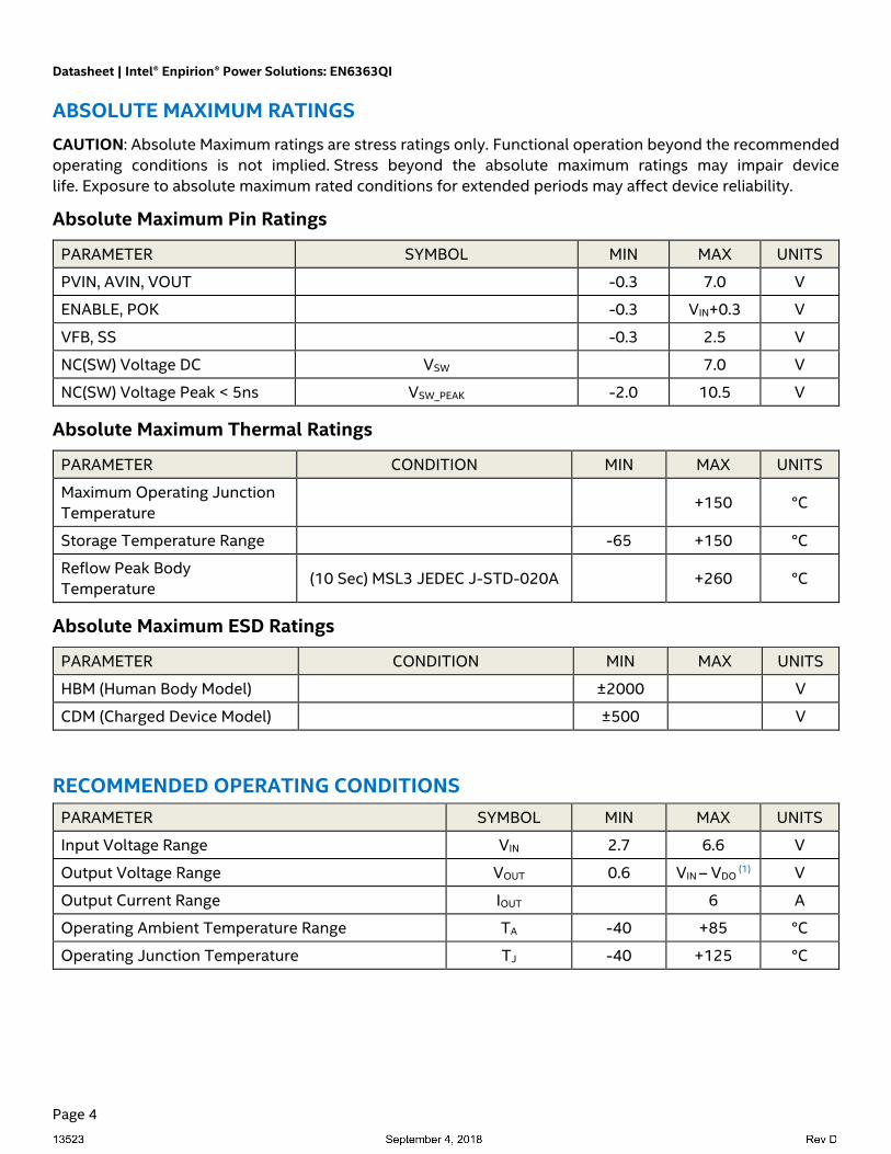
ABSOLUTE MAXIMUM RATINGS
CAUTION: Absolute Maximum ratings are stress ratings only. Functional operation beyond the recommended
operating conditions is not implied. Stress beyond the absolute maximum ratings may impair device
life. Exposure to absolute maximum rated conditions for extended periods may affect device reliability.
Absolute Maximum Pin Ratings
PARAMETER SYMBOL MIN MAX UNITS
PVIN, AVIN, VOUT -0.3 7.0 V
ENABLE, POK -0.3 VIN+0.3 V
VFB, SS -0.3 2.5 V
NC(SW) Voltage DC VSW 7.0 V
NC(SW) Voltage Peak < 5ns VSW_PEAK -2.0 10.5 V
Absolute Maximum Thermal Ratings
PARAMETER CONDITION MIN MAX UNITS
Maximum Operating Junction
Temperature +150 °C
Storage Temperature Range -65 +150 °C
Reflow Peak Body
Temperature (10 Sec) MSL3 JEDEC J-STD-020A +260 °C
Absolute Maximum ESD Ratings
PARAMETER CONDITION MIN MAX UNITS
HBM (Human Body Model) ±2000 V
CDM (Charged Device Model) ±500 V
RECOMMENDED OPERATING CONDITIONS
PARAMETER SYMBOL MIN MAX UNITS
Input Voltage Range VIN 2.7 6.6 V
Output Voltage Range VOUT 0.6 VIN – VDO (1) V
Output Current Range IOUT 6 A
Operating Ambient Temperature Range TA -40 +85 °C
Operating Junction Temperature TJ -40 +125 °C

Datasheet | Intel® Enpirion® Power Solutions: EN6363QI
Page 5
THERMAL CHARACTERISTICS
PARAMETER SYMBOL TYPICAL UNITS
Thermal Shutdown TSD 160 °C
Thermal Shutdown Hysteresis TSDHYS 25 °C
Thermal Resistance: Junction to Ambient (0 LFM) (2) JA 12.5 °C/W
Thermal Resistance: Junction to Case (0 LFM) JC 1 °C/W
(1) VDO (dropout voltage) is defined as (ILOAD x Droput Resistance). Please refer to Electrical Characteristics Table.
(2) Based on 2oz. external copper layers and proper thermal design in line with EIJ/JEDEC JESD51-7 standard for high
thermal conductivity boards.
Datasheet | Intel® Enpirion® Power Solutions: EN6363QI
Page 6
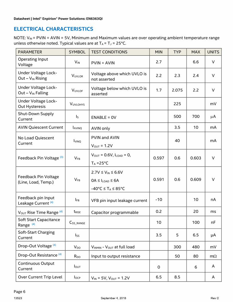
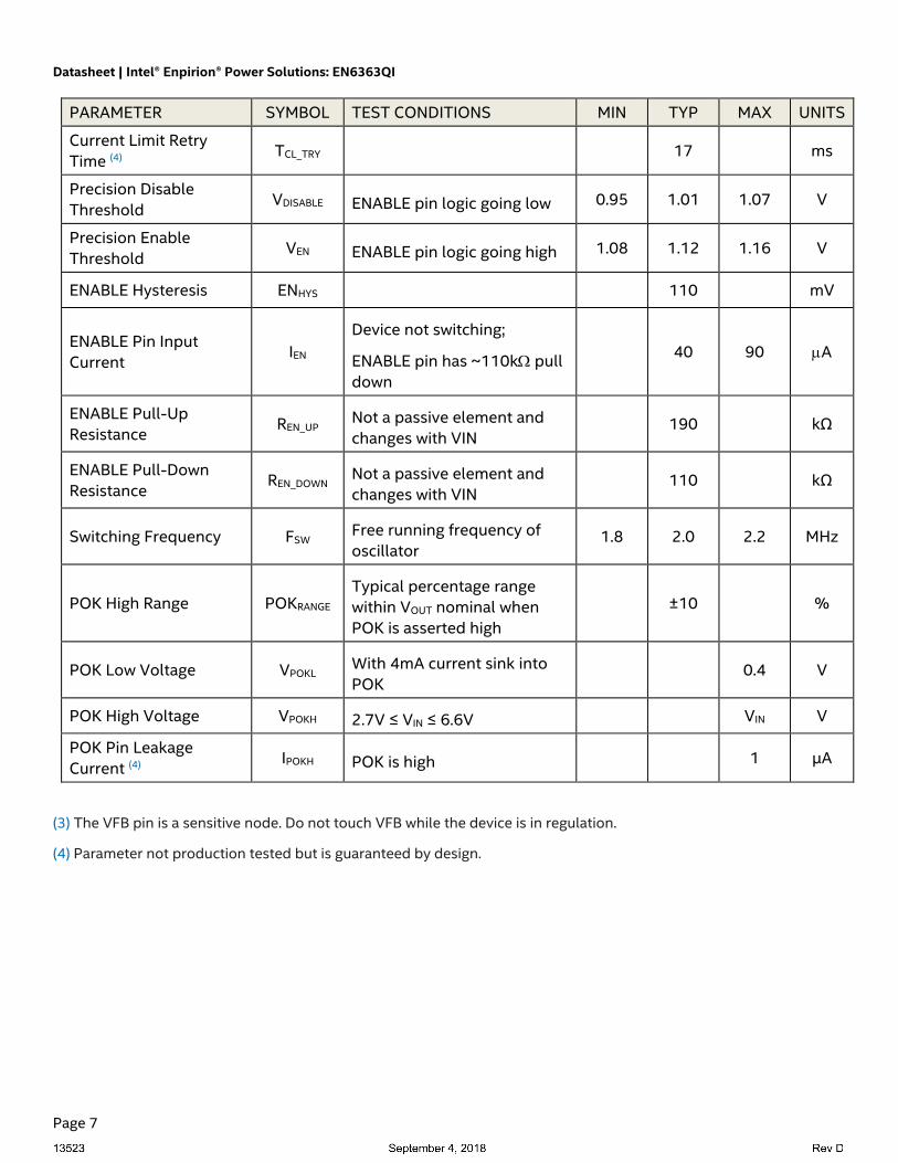
ELECTRICAL CHARACTERISTICS
NOTE: VIN = PVIN = AVIN = 5V, Minimum and Maximum values are over operating ambient temperature range
unless otherwise noted. Typical values are at TA = TJ = 25°C.
PARAMETER SYMBOL TEST CONDITIONS MIN TYP MAX UNITS
Operating Input
Voltage VIN PVIN = AVIN 2.7 6.6 V
Under Voltage Lock-
Out – VIN Rising VUVLOR Voltage above which UVLO is
not asserted 2.2 2.3 2.4 V
Under Voltage Lock-
Out – VIN Falling VUVLOF Voltage below which UVLO is
asserted 1.7 2.075 2.2 V
Under Voltage Lock-
Out Hysteresis VUVLOHYS 225 mV
Shut-Down Supply
Current IS ENABLE = 0V 500 700 A
AVIN Quiescent Current IAVINQ AVIN only 3.5 10 mA
No Load Quiescent
Current IVINQ
PVIN and AVIN
VOUT = 1.2V 40 mA
Feedback Pin Voltage (3) VFB VOUT = 0.6V, ILOAD = 0,
TA =25°C 0.597 0.6 0.603 V
Feedback Pin Voltage
(Line, Load, Temp.) VFB
2.7V ≤ VIN ≤ 6.6V
0A ≤ ILOAD ≤ 6A
-40°C ≤ TA ≤ 85°C
0.591 0.6 0.609 V
Feedback pin Input
Leakage Current (4) IFB VFB pin input leakage current -10 10 nA
VOUT Rise Time Range (4) tRISE Capacitor programmable 0.2 20 ms
Soft Start Capacitance
Range (4) CSS_RANGE 10 100 nF
Soft-Start Charging
Current ISS 3.5 5 6.5 µA
Drop-Out Voltage (4) VDO VINMIN - VOUT at full load 300 480 mV
Drop-Out Resistance (4) RDO Input to output resistance 50 80 m
Continuous Output
Current IOUT 0 6 A
Over Current Trip Level IOCP VIN = 5V, VOUT = 1.2V 6.5 8.5 A
Datasheet | Intel® Enpirion® Power Solutions: EN6363QI
Page 7
PARAMETER SYMBOL TEST CONDITIONS MIN TYP MAX UNITS
Current Limit Retry
Time (4) TCL_TRY 17 ms
Precision Disable
Threshold VDISABLE ENABLE pin logic going low 0.95 1.01 1.07 V
Precision Enable
Threshold VEN ENABLE pin logic going high 1.08 1.12 1.16 V
ENABLE Hysteresis ENHYS 110 mV
ENABLE Pin Input
Current IEN
Device not switching;
ENABLE pin has ~110k pull
down
40 90 A
ENABLE Pull-Up
Resistance REN_UP Not a passive element and
changes with VIN 190 kΩ
ENABLE Pull-Down
Resistance REN_DOWN Not a passive element and
changes with VIN 110 kΩ
Switching Frequency FSW Free running frequency of
oscillator 1.8 2.0 2.2 MHz
POK High Range POKRANGE Typical percentage range
within VOUT nominal when
POK is asserted high
±10 %
POK Low Voltage VPOKL With 4mA current sink into
POK 0.4 V
POK High Voltage VPOKH 2.7V ≤ VIN ≤ 6.6V VIN V
POK Pin Leakage
Current (4) IPOKH POK is high 1 µA
(3) The VFB pin is a sensitive node. Do not touch VFB while the device is in regulation.
(4) Parameter not production tested but is guaranteed by design.
Datasheet | Intel® Enpirion® Power Solutions: EN6363QI
Page 8
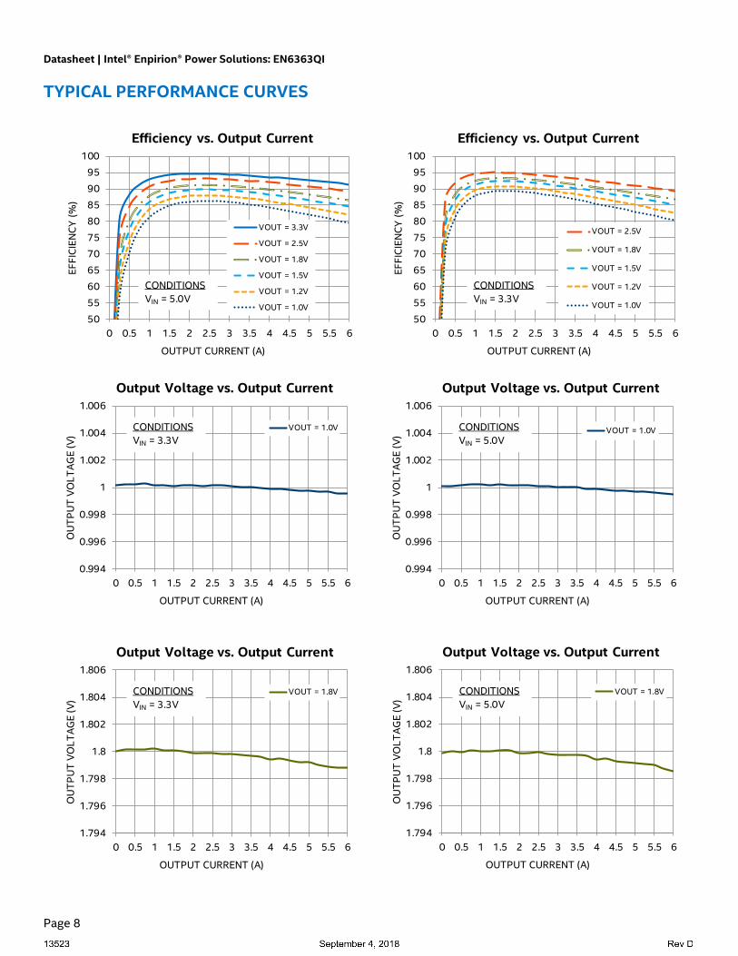
TYPICAL PERFORMANCE CURVES
50
55
60
65
70
75
80
85
90
95
100
0 0.5 1 1.5 2 2.5 3 3.5 4 4.5 5 5.5 6
EF
FIC
IEN
CY
(%
)
OUTPUT CURRENT (A)
Efficiency vs. Output Current
VOUT = 3.3V
VOUT = 2.5V
VOUT = 1.8V
VOUT = 1.5V
VOUT = 1.2V
VOUT = 1.0V
CONDITIONS
VIN = 5.0V
50
55
60
65
70
75
80
85
90
95
100
0 0.5 1 1.5 2 2.5 3 3.5 4 4.5 5 5.5 6
EF
FIC
IEN
CY
(%
)
OUTPUT CURRENT (A)
Efficiency vs. Output Current
VOUT = 2.5V
VOUT = 1.8V
VOUT = 1.5V
VOUT = 1.2V
VOUT = 1.0V
CONDITIONS
VIN = 3.3V
0.994
0.996
0.998
1
1.002
1.004
1.006
0 0.5 1 1.5 2 2.5 3 3.5 4 4.5 5 5.5 6
OU
TP
UT
VO
LT
AG
E (
V)
OUTPUT CURRENT (A)
Output Voltage vs. Output Current
VOUT = 1.0VCONDITIONS
VIN = 3.3V
0.994
0.996
0.998
1
1.002
1.004
1.006
0 0.5 1 1.5 2 2.5 3 3.5 4 4.5 5 5.5 6
OU
TP
UT
VO
LT
AG
E (
V)
OUTPUT CURRENT (A)
Output Voltage vs. Output Current
VOUT = 1.0VCONDITIONS
VIN = 5.0V
1.794
1.796
1.798
1.8
1.802
1.804
1.806
0 0.5 1 1.5 2 2.5 3 3.5 4 4.5 5 5.5 6
OU
TP
UT
VO
LT
AG
E (
V)
OUTPUT CURRENT (A)
Output Voltage vs. Output Current
VOUT = 1.8VCONDITIONS
VIN = 3.3V
1.794
1.796
1.798
1.8
1.802
1.804
1.806
0 0.5 1 1.5 2 2.5 3 3.5 4 4.5 5 5.5 6
OU
TP
UT
VO
LT
AG
E (
V)
OUTPUT CURRENT (A)
Output Voltage vs. Output Current
VOUT = 1.8VCONDITIONS
VIN = 5.0V
Datasheet | Intel® Enpirion® Power Solutions: EN6363QI
Page 9
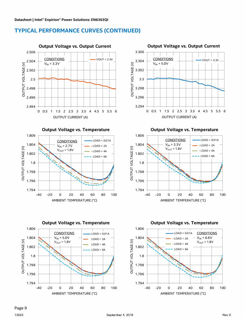
TYPICAL PERFORMANCE CURVES (CONTINUED)
2.494
2.496
2.498
2.5
2.502
2.504
2.506
0 0.5 1 1.5 2 2.5 3 3.5 4 4.5 5 5.5 6
OU
TP
UT
VO
LT
AG
E (
V)
OUTPUT CURRENT (A)
Output Voltage vs. Output Current
VOUT = 2.5VCONDITIONS
VIN = 3.3V
3.294
3.296
3.298
3.3
3.302
3.304
3.306
0 0.5 1 1.5 2 2.5 3 3.5 4 4.5 5 5.5 6
OU
TP
UT
VO
LT
AG
E (
V)
OUTPUT CURRENT (A)
Output Voltage vs. Output Current
VOUT = 3.3VCONDITIONS
VIN = 5.0V
1.794
1.796
1.798
1.8
1.802
1.804
1.806
-40 -20 0 20 40 60 80 100
OU
TP
UT
VO
LT
AG
E (
V)
AMBIENT TEMPERATURE ( C)
Output Voltage vs. Temperature
LOAD = 0.01A
LOAD = 2A
LOAD = 4A
LOAD = 6A
CONDITIONS
VIN = 2.7VVOUT = 1.8V
1.794
1.796
1.798
1.8
1.802
1.804
1.806
-40 -20 0 20 40 60 80 100
OU
TP
UT
VO
LT
AG
E (
V)
AMBIENT TEMPERATURE ( C)
Output Voltage vs. Temperature
LOAD = 0.01A
LOAD = 2A
LOAD = 4A
LOAD = 6A
CONDITIONS
VIN = 3.3VVOUT = 1.8V
1.794
1.796
1.798
1.8
1.802
1.804
1.806
-40 -20 0 20 40 60 80 100
OU
TP
UT
VO
LT
AG
E (
V)
AMBIENT TEMPERATURE ( C)
Output Voltage vs. Temperature
LOAD = 0.01A
LOAD = 2A
LOAD = 4A
LOAD = 6A
CONDITIONS
VIN = 5.0VVOUT = 1.8V
1.794
1.796
1.798
1.8
1.802
1.804
1.806
-40 -20 0 20 40 60 80 100
OU
TP
UT
VO
LT
AG
E (
V)
AMBIENT TEMPERATURE ( C)
Output Voltage vs. Temperature
LOAD = 0.01A
LOAD = 2A
LOAD = 4A
LOAD = 6A
CONDITIONS
VIN = 6.6VVOUT = 1.8V
Datasheet | Intel® Enpirion® Power Solutions: EN6363QI
Page 10
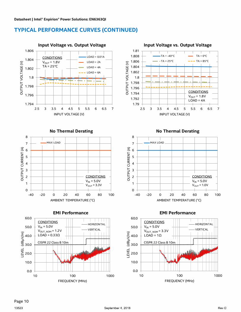
TYPICAL PERFORMANCE CURVES (CONTINUED)
1.794
1.796
1.798
1.8
1.802
1.804
1.806
2.5 3 3.5 4 4.5 5 5.5 6 6.5 7
OU
TP
UT
VO
LT
AG
E (
V)
INPUT VOLTAGE (V)
Input Voltage vs. Output Voltage
LOAD = 0.01A
LOAD = 2A
LOAD = 4A
LOAD = 6A
CONDITIONS
VOUT = 1.8VTA = 25°C
1.79
1.792
1.794
1.796
1.798
1.8
1.802
1.804
1.806
1.808
1.81
2.5 3 3.5 4 4.5 5 5.5 6 6.5 7
OU
TP
UT
VO
LT
AG
E (
V)
INPUT VOLTAGE (V)
Input Voltage vs. Output Voltage
TA = -40°C TA = 0°C
TA = 25°C TA = 85°C
CONDITIONS
VOUT = 1.8V
LOAD = 4A
0
1
2
3
4
5
6
7
8
-40 -20 0 20 40 60 80 100
OU
TP
UT
CU
RR
EN
T (
A)
AMBIENT TEMPERATURE ( C)
No Thermal Derating
MAX LOAD
CONDITIONS
VIN = 5.0VVOUT = 3.3V
0
1
2
3
4
5
6
7
8
-40 -20 0 20 40 60 80 100
OU
TP
UT
CU
RR
EN
T (
A)
AMBIENT TEMPERATURE ( C)
No Thermal Derating
MAX LOAD
CONDITIONS
VIN = 5.0VVOUT = 1.0V
0.0
10.0
20.0
30.0
40.0
50.0
60.0
10 100 1000
LE
VE
L (
dB
µV
/m)
FREQUENCY (MHz)
EMI Performance
HORIZONTAL
VERTICAL
CISPR 22 Class B 10m
CONDITIONS
VIN = 5.0V
VOUT_NOM = 1.2V
LOAD = 0.33Ω
0.0
10.0
20.0
30.0
40.0
50.0
60.0
10 100 1000
LE
VE
L (
dB
µV
/m)
FREQUENCY (MHz)
EMI Performance
HORIZONTAL
VERTICAL
CISPR 22 Class B 10m
CONDITIONS
VIN = 5.0VVOUT_NOM = 3.3V
LOAD = 1Ω
Datasheet | Intel® Enpirion® Power Solutions: EN6363QI
Page 11
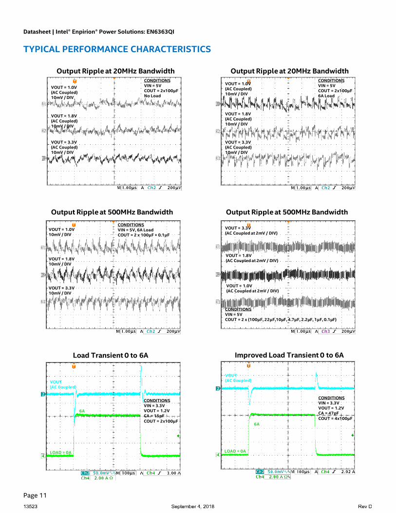
TYPICAL PERFORMANCE CHARACTERISTICS
VOUT = 1.0V(AC Coupled)10mV / DIV
Output Ripple at 20MHz BandwidthCONDITIONSVIN = 5VCOUT = 2x100µFNo Load
VOUT = 1.8V(AC Coupled)10mV / DIV
VOUT = 3.3V(AC Coupled)10mV / DIV
VOUT = 1.0V(AC Coupled)10mV / DIV
Output Ripple at 20MHz BandwidthCONDITIONSVIN = 5VCOUT = 2x100µF6A Load
VOUT = 1.8V(AC Coupled)10mV / DIV
VOUT = 3.3V(AC Coupled)10mV / DIV
VOUT = 1.0V10mV / DIV
Output Ripple at 500MHz Bandwidth
CONDITIONSVIN = 5V, 6A LoadCOUT = 2 x 100µF + 0.1µF
VOUT = 1.8V10mV / DIV
VOUT = 3.3V10mV / DIV
VOUT = 3.3V(AC Coupled at 2mV / DIV)
Output Ripple at 500MHz Bandwidth
CONDITIONSVIN = 5VCOUT = 2 x (100µF, 22µF,10µF, 4.7µF, 2.2µF, 1µF, 0.1µF)
VOUT = 1.8V(AC Coupled at 2mV / DIV)
VOUT = 1.0V(AC Coupled at 2mV / DIV)
VOUT(AC Coupled)
Load Transient 0 to 6A
CONDITIONSVIN = 3.3VVOUT = 1.2VCA = 15pF
COUT = 2x100µF
LOAD = 0A
6A
VOUT(AC Coupled)
Improved Load Transient 0 to 6A
CONDITIONSVIN = 3.3VVOUT = 1.2VCA = 47pFCOUT = 4x100µF
LOAD = 0A
6A
Datasheet | Intel® Enpirion® Power Solutions: EN6363QI
Page 12
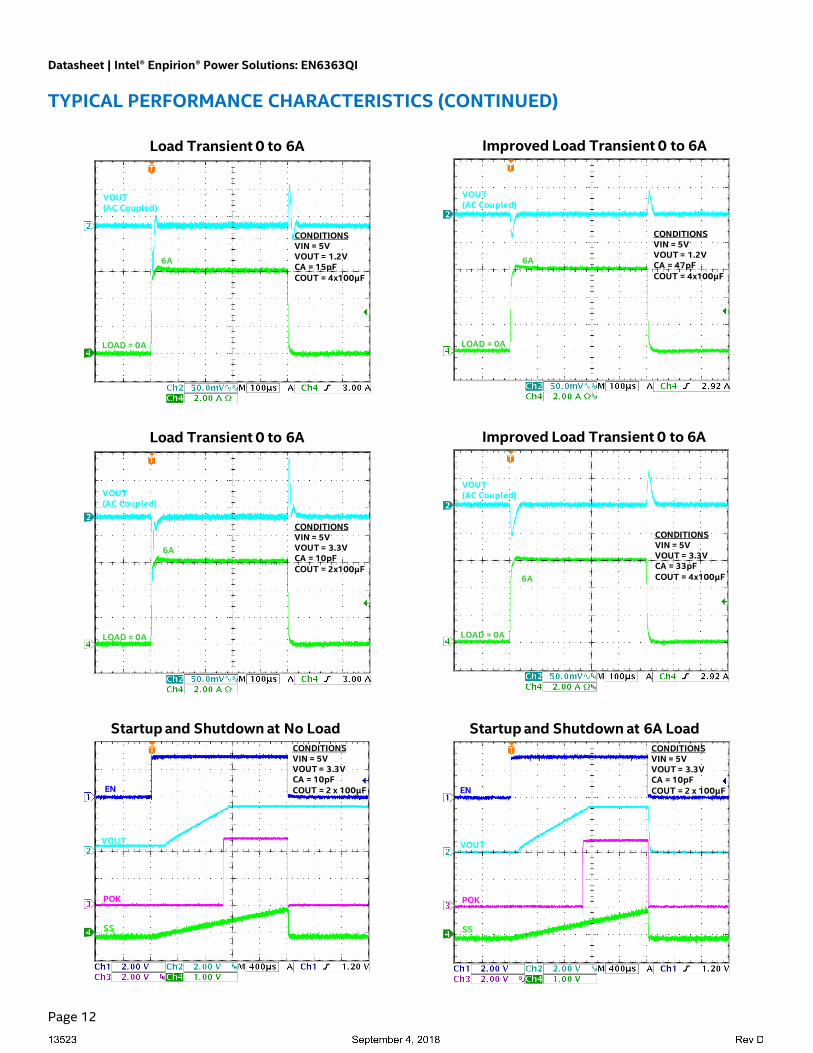
TYPICAL PERFORMANCE CHARACTERISTICS (CONTINUED)
VOUT(AC Coupled)
CONDITIONSVIN = 5VVOUT = 1.2VCA = 15pF
COUT = 4x100µF
LOAD = 0A
6A
Load Transient 0 to 6A
VOUT(AC Coupled)
Improved Load Transient 0 to 6A
CONDITIONSVIN = 5VVOUT = 1.2VCA = 47pFCOUT = 4x100µF
LOAD = 0A
6A
VOUT(AC Coupled)
CONDITIONSVIN = 5VVOUT = 3.3VCA = 10pF
COUT = 2x100µF
LOAD = 0A
6A
Load Transient 0 to 6A
VOUT(AC Coupled)
Improved Load Transient 0 to 6A
CONDITIONSVIN = 5VVOUT = 3.3VCA = 33pFCOUT = 4x100µF
LOAD = 0A
6A
EN
Startup and Shutdown at No LoadCONDITIONSVIN = 5VVOUT = 3.3VCA = 10pF
COUT = 2 x 100µF
VOUT
POK
SS
EN
Startup and Shutdown at 6A Load
VOUT
POK
SS
CONDITIONSVIN = 5VVOUT = 3.3VCA = 10pF
COUT = 2 x 100µF
Datasheet | Intel® Enpirion® Power Solutions: EN6363QI
Page 13
TYPICAL PERFORMANCE CHARACTERISTICS (CONTINUED)
PVIN
PVIN Startup at No LoadCONDITIONSVIN = 5VVOUT = 3.3VCA = 10pFCOUT = 2 x 100µF
VOUT
POK
SS
PVIN
PVIN Shutdown at No Load
CONDITIONSVIN = 5VVOUT = 3.3VCA = 10pF
COUT = 2 x 100µFVOUT
POK
SS
PVIN
PVIN Startup at 6A Load
CONDITIONSVIN = 5VVOUT = 1VCA = 15pFCOUT = 2 x 100µF
VOUT
POK
LOAD
PVIN
PVIN Shutdown at 6A Load
CONDITIONSVIN = 5VVOUT = 1VCA = 15pF
COUT = 2 x 100µFVOUT
POK
LOAD
EN
Pre-Bias Startup
CONDITIONSVIN = 5VVOUT = 1V
VOUT
POK
50% Pre-Bias
10% Pre-Bias
90% Pre-Bias
EN
Pre-Bias Startup
CONDITIONSVIN = 5VVOUT = 3.3V
VOUT
POK
50% Pre-Bias
10% Pre-Bias
90% Pre-Bias
Datasheet | Intel® Enpirion® Power Solutions: EN6363QI
Page 14
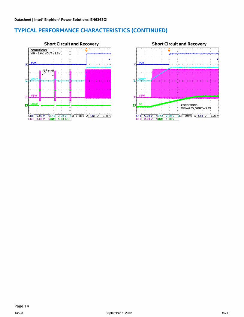
TYPICAL PERFORMANCE CHARACTERISTICS (CONTINUED)
POK
Short Circuit and Recovery
CONDITIONSVIN = 6.6V, VOUT = 3.3V
VOUT
VSW
LOAD
“Re-Try”
POK
Short Circuit and Recovery
CONDITIONSVIN = 6.6V, VOUT = 3.3V
VOUT
VSW
SS
Datasheet | Intel® Enpirion® Power Solutions: EN6363QI
Page 15
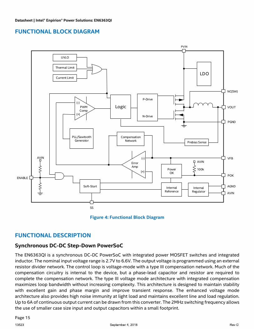
FUNCTIONAL BLOCK DIAGRAM
Figure 4: Functional Block Diagram
FUNCTIONAL DESCRIPTION
Synchronous DC-DC Step-Down PowerSoC
The EN6363QI is a synchronous DC-DC PowerSoC with integrated power MOSFET switches and integrated
inductor. The nominal input voltage range is 2.7V to 6.6V. The output voltage is programmed using an external
resistor divider network. The control loop is voltage-mode with a type III compensation network. Much of the
compensation circuitry is internal to the device, but a phase-lead capacitor and resistor are required to
complete the compensation network. The type III voltage mode architecture with integrated compensation
maximizes loop bandwidth without increasing complexity. This architecture is designed to maintain stability
with excellent gain and phase margin and improve transient response. The enhanced voltage mode
architecture also provides high noise immunity at light load and maintains excellent line and load regulation.
Up to 6A of continuous output current can be drawn from this converter. The 2MHz switching frequency allows
the use of smaller case size input and output capacitors within a small footprint.
(+)
(-)
Error Amp
VFB
VOUT
P-Drive
N-Drive
UVLO
Thermal Limit
Soft-Start
PLL/SawtoothGenerator
(+)
(-)
PWM Comp
PVIN
ENABLE
PGND
Logic
CompensationNetwork
NC(SW)
AVIN
AGNDInternal
RegulatorInternal
Reference
SS
PowerOK
POK
Current Limit
Prebias Sense
LDO
AVIN
AVIN
100k
Datasheet | Intel® Enpirion® Power Solutions: EN6363QI
Page 16
The EN6363QI architecture includes the following features.
Operational Features:
• Precision enable circuit with tight threshold range
• Soft-start circuit allowing controlled startup when the converter is initially powered up
• Power OK circuit indicating the output voltage is greater than 90% of programmed value
Protection Features:
• Over-current protection from short circuit or excessive load current
• Thermal shutdown with hysteresis to prevent over temperature stress
• Output voltage pre-bias startup protection for smooth monotonic startup
• Under-voltage lockout protection to prevent under-voltage operation
Precision Enable Operation
The enable (ENABLE) pin provides a mean to startup or to shutdown the device. When the ENABLE pin is
asserted high, the device will undergo a normal soft-start where the output will rise monotonically into
regulation. Asserting a logic low on this pin will deactivate the device by turning off the internal power switches
and the POK flag will also be pulled low. The ENABLE pin is connected through an internal divider network to
AVIN and AGND. If left floating, the ENABLE voltage will be equal to the AVIN voltage and the value set by the
divider network ratio (~2.5):
VEN (FLOATING) ≈ AVIN / 2.5
The precision enable circuit ensures the device will enable or disable within a tight voltage range for both high
or low logic. In order to ensure a known state the ENABLE pin should be pulled high or low. See the Electrical
Characteristics Table for technical specifications for the ENABLE pin.
Soft-Start Operation
The soft-start circuitry will reduce inrush current during startup as the regulator charges the output voltage up
to nominal level gradually. The output rise time is controlled by the soft-start capacitor, which is placed
between the SS pin and the AGND pin. When the part is enabled, the soft-start (SS) current generator charges
the SS capacitor in a linear manner. Once the voltage on the SS capacitor reaches 0.6V, the controller selects
the intenral bandgap voltage as the reference. The voltage across the SS capacitor will continue ramping up
until it reaches around 1.27V. The rise time is defined as the time needed by the output voltage to go from
zero to the programmed value. The rise time (tRISE) is given by the following equation:
tRISE [ms] = Css [nF] x 0.13
With a 10nF soft-start capacitance on the SS pin, the soft-start rise time will be set to 1.3ms. The recommended
range for the value of the SS capacitor is between 10nF and 100nF. Note that excessive bulk capacitance on
the output can cause an over current event on startup if the soft-start time is too low. Refer to the
Compensation and Transient Response section for details on proper bulk capacitance usage.
POK Operation
The Power OK (POK) is an open drain signal (with internal 100kΩ pull-up to AVIN) to indicate if the output
voltage is within the specified range. POK is asserted high when the rising output voltage exceeds 90% of the
programmed output voltage. For a stronger pull-up, an external resistor may be connected to AVIN. If the
Datasheet | Intel® Enpirion® Power Solutions: EN6363QI
Page 17
nominal output voltage falls outside the set range (typically 90% to 110% of nominal) the POK signal will be
asserted low by an internal 4mA pull-down transistor.
Over-Current Protection (OCP)
The current limit function is achieved by sensing the current flowing through the topside power PFET. When
the sensed current exceeds the over current trip point (see Electrical Characteristics Table), both power FETs
are turned off for the remainder of the switching cycle. If the over-current condition is removed, the over-
current protection circuit will enable normal PWM operation. In the event the OCP circuit trips at least 7
consecutive PWM cycles, the device enters a retry mode; the device is disabled for about 17ms and restarted
with a normal soft-start. This cycle can continue indefinitely as long as the over current condition persists. The
OCP circuit will disable operation and protect the device from excessive current during operation without
compromising the full load capability of the device.
Thermal Protection
The thermal shutdown circuit disables the device operation (switching stops) when the junction temperature
exceeds 160°C. When the junction temperature drops by approximately 25°C, the converter will re-start with
a normal soft-start. By preventing operation at excessive temperatures, the thermal shutdown circuit will
protect the device from overstress.
Pre-Bias Startup Protection
The EN6363QI supports startup into a pre-biased output. A proprietary circuit ensures the output voltage rises
from the pre-bias voltage level to the programmed output voltage on startup. During this soft-start period, the
voltage rise is monotonic for output voltage range from 0% to 90% of nominal. If the pre-bias voltage is above
90% on startup, there might be a slight dip (~3%) in output voltage before it rises monotonically. If the pre-
bias voltage is above 100% of nominal during startup, the device will not switch until the soft-start period is
over. Note that when the device begins switching and the pre-bias output voltage is higher than nominal, the
bottomside NFET will discharge the output quickly (but limited to 2-cycles to prevent excessive current) to
bring the voltage back into regulation. The pre-bias protection circuit is designed to prevent improper behavior
on startup regardless of the pre-bias output voltage during soft-start.
Input Under-Voltage Lock-Out (UVLO)
When the device input voltage falls below UVLO, switching is disabled to prevent operation at insufficient
voltage levels. During startup, the UVLO circuit ensures that the converter will not start switching until the
input voltage is above the specified minimum voltage. Hysteresis and input de-glitch circuits are incorporated
in order to ensure high noise immunity and prevent a false trigger in the UVLO voltage region.
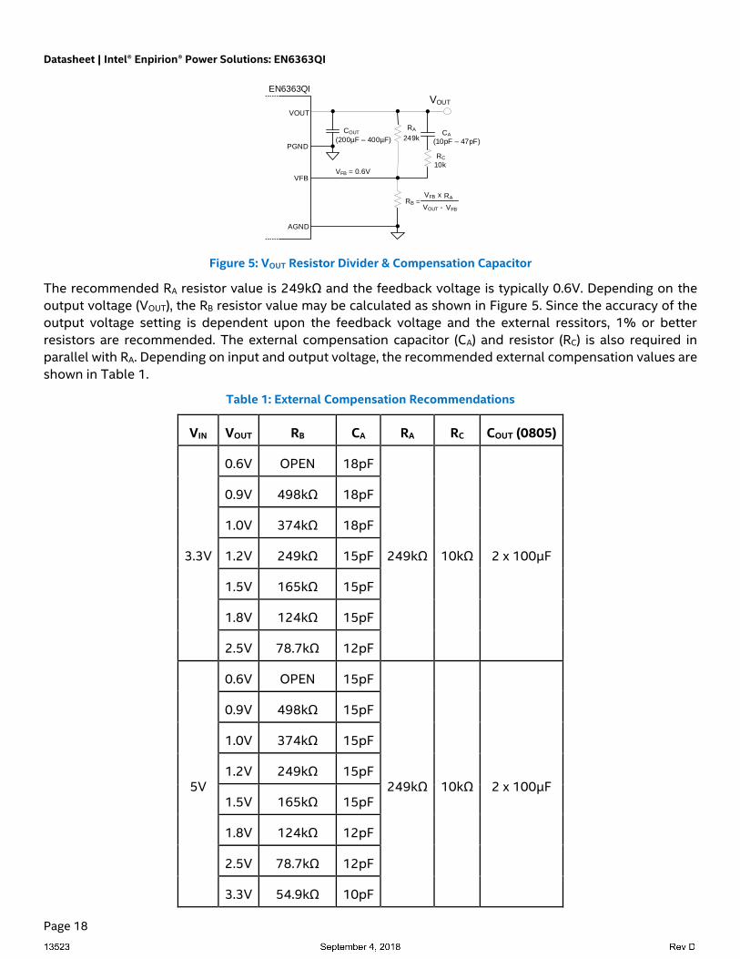
APPLICATION INFORMATION
Output Voltage Setting
The EN6363QI output voltage is programmed using a simple resistor divider network (RA and RB). Figure 5
shows the resistor divider configuration.
Datasheet | Intel® Enpirion® Power Solutions: EN6363QI
Page 18
Figure 5: VOUT Resistor Divider & Compensation Capacitor
The recommended RA resistor value is 249kΩ and the feedback voltage is typically 0.6V. Depending on the
output voltage (VOUT), the RB resistor value may be calculated as shown in Figure 5. Since the accuracy of the
output voltage setting is dependent upon the feedback voltage and the external ressitors, 1% or better
resistors are recommended. The external compensation capacitor (CA) and resistor (RC) is also required in
parallel with RA. Depending on input and output voltage, the recommended external compensation values are
shown in Table 1.
Table 1: External Compensation Recommendations
VIN VOUT RB CA RA RC COUT (0805)
3.3V
0.6V OPEN 18pF
249kΩ 10kΩ 2 x 100µF
0.9V 498kΩ 18pF
1.0V 374kΩ 18pF
1.2V 249kΩ 15pF
1.5V 165kΩ 15pF
1.8V 124kΩ 15pF
2.5V 78.7kΩ 12pF
5V
0.6V OPEN 15pF
249kΩ 10kΩ 2 x 100µF
0.9V 498kΩ 15pF
1.0V 374kΩ 15pF
1.2V 249kΩ 15pF
1.5V 165kΩ 15pF
1.8V 124kΩ 12pF
2.5V 78.7kΩ 12pF
3.3V 54.9kΩ 10pF
VOUT
VOUT
PGND
VFB
RA
RC
CACOUT
VFB = 0.6V
EN6363QI
RB
RAVFB
VFBVOUT
x
-=
AGND
(200µF – 400µF) (10pF – 47pF)
10k
249k
Datasheet | Intel® Enpirion® Power Solutions: EN6363QI
Page 19
Compensation and Transient Response
The EN6363QI uses an enhanced type III voltage mode control architecture. Most of the compensation is
internal, which simplifies the design. In some applications, improved transient performance may be desired
with additional output capacitors (COUT). In such an instance, the phase-lead capacitor (CA) can be adjusted
depending on the total output capacitance. Using Table 1 as the reference for CA, if COUT is increased, then the
CA should also be increased. The relationship is linearly shown below:
ΔCOUT ≈ +100µF ΔCA ≈ +10pF
As COUT increases and the CA value is adjusted, the device bandwidth will reach its optimization level (at around
1/10th of the switching frequency). As shown in Table 1, the recommended CA value is lower for the 5V input
than 3.3V input. This is to ensure that the loop bandwidth is not over extended due to the increased gain at
the higher input voltage range. The CA value may be extrapolated for other input voltages. The limitation for
adjusting the compensation is based on diminished return. Further adjustments by increasing COUT and
increasing CA may not yield better transient response or in some situations cause lower gain and phase margin.
Over compensating with excessive output capacitance may also cause the device to trigger current limit on
startup due to the energy required to charge the output up to regulation level. Due to such limitations, the
recommended maximum output capacitance (COUT_MAX) is 400µF and the recommended maximum phase-lead
capacitance (CA_MAX) is 47pF.
Input Capacitor Selection
The input of synchronous buck regulators can be very noisy and should be decoupled properly in order to
ensure stable operation. In addition, input parasitic line inductance can attribute to higher input voltage ripple.
The EN6363QI requires a minimum of 2 x 47µF 0805 input capacitors. As the distance of the input power
source to the input of the EN6363QI is increased, it is recommended to increase input capacitance in order to
mitigate the line inductance from the source. Low-ESR ceramic capacitors should be used. The dielectric must
be X5R or X7R rated and the size must be at least 0805 (EIA) due to derating. Y5V or equivalent dielectric
formulations must not be used as these lose too much capacitance with frequency, temperature and bias
voltage. In some applications, lower value capacitors are needed in parallel with the larger capacitors in order
to provide high frequency decoupling. Larger electrolytic or tantalum bulk capacitors may be used in
conjunction to increase total input capacitance but should not be used solely as a replacement for the ceramic
capacitors.
Table 2: Recommended Input Capacitors
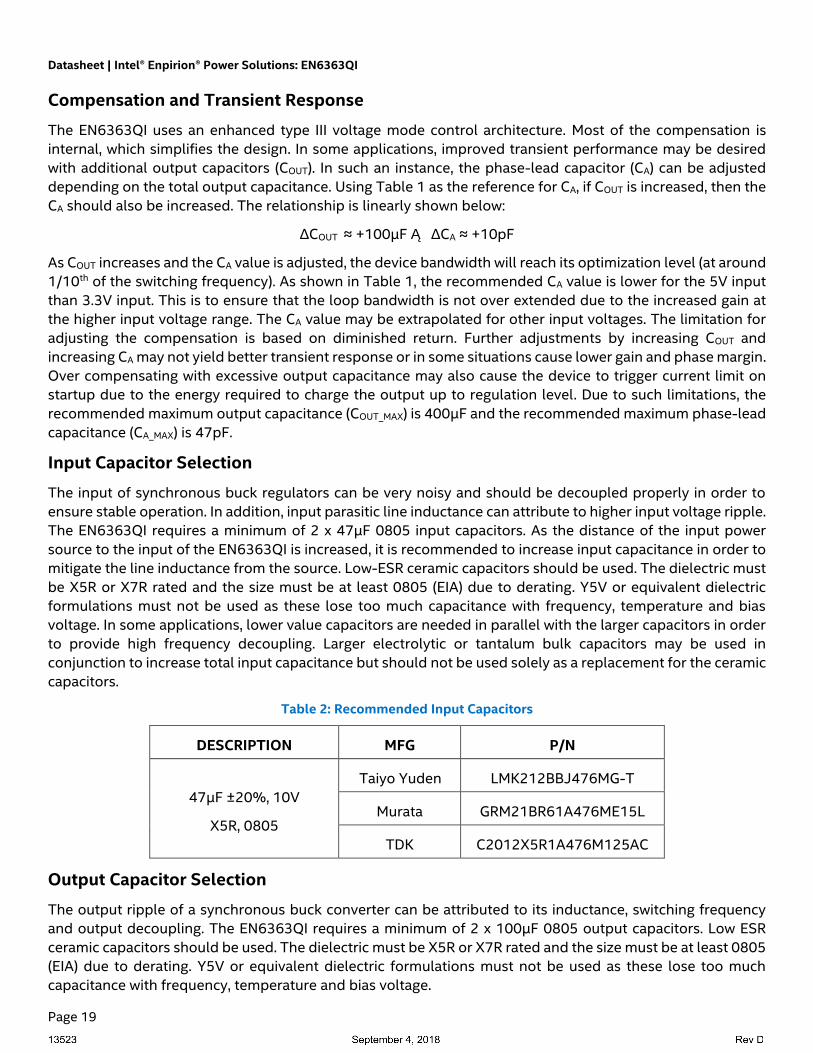
DESCRIPTION MFG P/N
47µF ±20%, 10V
X5R, 0805
Taiyo Yuden LMK212BBJ476MG-T
Murata GRM21BR61A476ME15L
TDK C2012X5R1A476M125AC
Output Capacitor Selection
The output ripple of a synchronous buck converter can be attributed to its inductance, switching frequency
and output decoupling. The EN6363QI requires a minimum of 2 x 100µF 0805 output capacitors. Low ESR
ceramic capacitors should be used. The dielectric must be X5R or X7R rated and the size must be at least 0805
(EIA) due to derating. Y5V or equivalent dielectric formulations must not be used as these lose too much
capacitance with frequency, temperature and bias voltage.
Datasheet | Intel® Enpirion® Power Solutions: EN6363QI
Page 20
Table 3: Recommended Output Capacitors
DESCRIPTION MFG P/N
100µF ±20%, 6.3V,
X5R, 0805 Murata GRM21BR60J107ME15L
Output ripple voltage is determined by the aggregate output capacitor impedance. Output impedance,
denoted as Z, is comprised of effective series resistance (ESR) and effective series inductance (ESL):
Z = ESR + ESL
The resonant frequency of a ceramic capacitor is inversely proportional to the capacitance. Lower capacitance
corresponds to higher resonant frequency. When two capacitors are placed in parallel, the benefit of both are
combined. It is beneficial to decouple the output with capacitors of various capacitance and size. Placing them
all in parallel reduces the impedance and will hence result in lower output ripple.
nTotal ZZZZ
1...
111
21
THERMAL CONSIDERATIONS
Thermal considerations are important elements of power supply design. Whenever there are power losses in
a system, the heat that is generated by the power dissipation needs to be taken into account. The Intel Enpirion
PowerSoC technology helps alleviate some of those concerns.
The EN6363QI DC-DC converter is packaged in a 4mm x 6mm x 2.5mm 34-pin QFN package. The QFN package
is constructed with copper lead frames that have exposed thermal pads. The exposed thermal pad on the
package should be soldered directly on to a copper ground pad on the printed circuit board (PCB) to act as a
heat sink. The recommended maximum junction temperature for continuous operation is 125°C. Continuous
operation above 125°C may reduce long-term reliability. The device has a thermal overload protection circuit
designed to turn off the device at an approximate junction temperature value of 160°C.
The following example and calculations illustrate the thermal performance of the EN6363QI with the following
parameters:
VIN = 5V
VOUT = 3.3V
IOUT = 6A
First, calculate the output power.
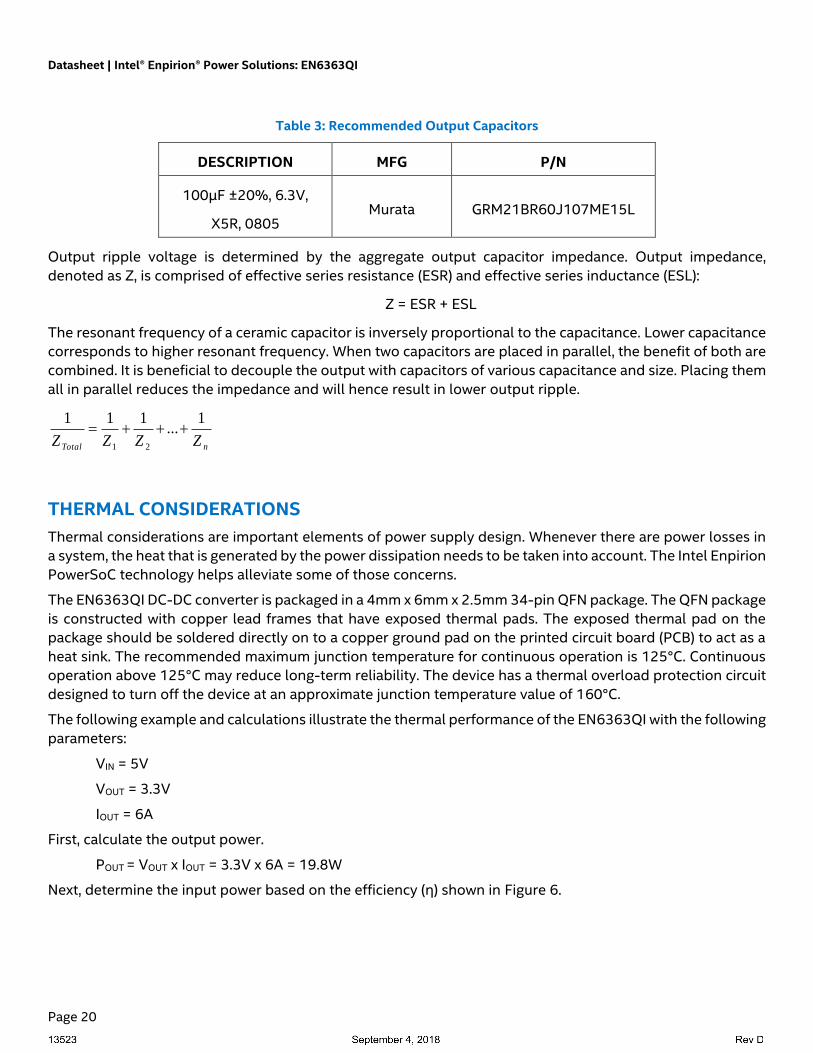
POUT = VOUT x IOUT = 3.3V x 6A = 19.8W
Next, determine the input power based on the efficiency (η) shown in Figure 6.
Datasheet | Intel® Enpirion® Power Solutions: EN6363QI
Page 21
Figure 6: Efficiency vs. Output Current
For VIN = 5V, VOUT = 3.3V at 6A, η ≈ 91%
η = POUT / PIN = 91% = 0.91
PIN = POUT / η
PIN ≈ 19.8W / 0.91 ≈ 21.76W ≈ 21.8W
The power dissipation (PD) is the power loss in the system and can be calculated by subtracting the output
power from the input power.
PD = PIN – POUT
= 21.8W – 19.8W ≈ 2W
With the power dissipation known, the temperature rise in the device may be estimated based on the theta JA
value (θJA). The θJA parameter estimates how much the temperature will rise in the device for every watt of
power dissipation. The EN6363QI has a θJA value of 12.5°C/W without airflow.
Determine the change in temperature (ΔT) based on PD and θJA.
ΔT = PD x θJA
ΔT ≈ 2W x 12.5°C/W ≈ 25°C
The junction temperature (TJ) of the device is approximately the ambient temperature (TA) plus the change in
temperature. We assume the initial ambient temperature to be 25°C.
TJ = TA + ΔT
TJ ≈ 25°C + 25°C ≈ 50°C
The maximum operating junction temperature (TJMAX) of the device is 125°C, so the device can operate at a
higher ambient temperature. The maximum ambient temperature (TAMAX) allowed can be calculated.
TAMAX = TJMAX – PD x θJA
≈ 125°C – 25°C ≈ 100°C
The maximum ambient temperature the device can reach is 100°C given the input and output conditions. Note
that the efficiency will be slightly lower at higher temperatures and this calculation is an estimate.
50
55
60
65
70
75
80
85
90
95
100
0 0.5 1 1.5 2 2.5 3 3.5 4 4.5 5 5.5 6
EF
FIC
IEN
CY
(%
)
OUTPUT CURRENT (A)
Efficiency vs. Output Current
VOUT = 3.3VCONDITIONSVIN = 5.0V
Datasheet | Intel® Enpirion® Power Solutions: EN6363QI
Page 22
APPLICATION CIRCUITS
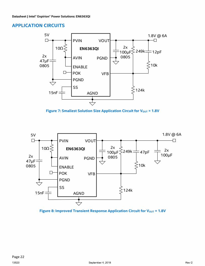
Figure 7: Smallest Solution Size Application Circuit for VOUT = 1.8V
Figure 8: Improved Transient Response Application Circuit for VOUT = 1.8V
1.8V @ 6A5V
2x47µF0805
VOUT
AVIN
AGND
SS
PVIN
ENABLE
PGND
PGND
EN6363QI
15nF
VFB
2x100µF0805
10Ω
POK
249k 12pF
10k
124k
1.8V @ 6A5V
2x47µF0805
VOUT
AVIN
AGND
SS
PVIN
ENABLE
PGND
PGND
EN6363QI
15nF
VFB
2x100µF0805
10Ω
POK
249k 47pF
10k
124k
2x100µF
Datasheet | Intel® Enpirion® Power Solutions: EN6363QI
Page 23
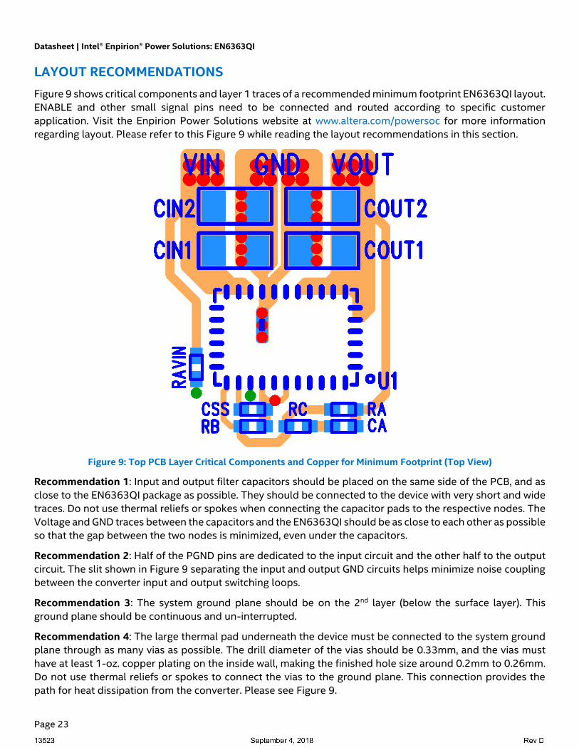
LAYOUT RECOMMENDATIONS
Figure 9 shows critical components and layer 1 traces of a recommended minimum footprint EN6363QI layout.
ENABLE and other small signal pins need to be connected and routed according to specific customer
application. Visit the Enpirion Power Solutions website at www.altera.com/powersoc for more information
regarding layout. Please refer to this Figure 9 while reading the layout recommendations in this section.
Figure 9: Top PCB Layer Critical Components and Copper for Minimum Footprint (Top View)
Recommendation 1: Input and output filter capacitors should be placed on the same side of the PCB, and as
close to the EN6363QI package as possible. They should be connected to the device with very short and wide
traces. Do not use thermal reliefs or spokes when connecting the capacitor pads to the respective nodes. The
Voltage and GND traces between the capacitors and the EN6363QI should be as close to each other as possible
so that the gap between the two nodes is minimized, even under the capacitors.
Recommendation 2: Half of the PGND pins are dedicated to the input circuit and the other half to the output
circuit. The slit shown in Figure 9 separating the input and output GND circuits helps minimize noise coupling
between the converter input and output switching loops.
Recommendation 3: The system ground plane should be on the 2nd layer (below the surface layer). This
ground plane should be continuous and un-interrupted.
Recommendation 4: The large thermal pad underneath the device must be connected to the system ground
plane through as many vias as possible. The drill diameter of the vias should be 0.33mm, and the vias must
have at least 1-oz. copper plating on the inside wall, making the finished hole size around 0.2mm to 0.26mm.
Do not use thermal reliefs or spokes to connect the vias to the ground plane. This connection provides the
path for heat dissipation from the converter. Please see Figure 9.
Datasheet | Intel® Enpirion® Power Solutions: EN6363QI
Page 24
Recommendation 5: Multiple small vias (the same size as the thermal vias discussed in recommendation 4
should be used to connect ground terminal of the input capacitor and output capacitors to the system ground
plane. Put the vias under the capacitors along the edge of the GND copper closest to the Voltage copper.
Please see Figure 9. These vias connect the input/output filter capacitors to the GND plane, and help reduce
parasitic inductances in the input and output current loops. If the vias cannot be placed under CIN and COUT,
then put them just outside the capacitors along the GND slit separating the two components. Do not use
thermal reliefs or spokes to connect these vias to the ground plane.
Recommendation 6: AVIN is the power supply for the internal small-signal control circuits. It should be
connected to the input voltage at a quiet point. In Figure 9 this connection is made at the input capacitor
furthest from the PVIN pin and on the input source side. Avoid connecting AVIN near the PVIN pin even though
it is the same node as the input ripple is higher there.
Recommendation 7: The VOUT sense point should be connected at the last output filter capacitor furthest from
the VOUT pins. Keep the sense trace as short as possible in order to avoid noise coupling into the control loop.
Recommendation 8: Keep RA, CA, RC and RB close to the VFB pin (see Figure 9). The VFB pin is a high-impedance,
sensitive node. Keep the trace to this pin as short as possible. Whenever possible, connect RB directly to the
AGND pin instead of going through the GND plane. The AGND should connect to the PGND at a single point
from the AGND pin to the PGND plane on the 2nd layer.
Recommendation 9: The layer 1 metal under the device must not be more than shown in Figure 9. See the
following section regarding Exposed Metal on Bottom of Package. As with any switch-mode DC-DC converter,
try not to run sensitive signal or control lines underneath the converter package on other layers.
Datasheet | Intel® Enpirion® Power Solutions: EN6363QI
Page 25
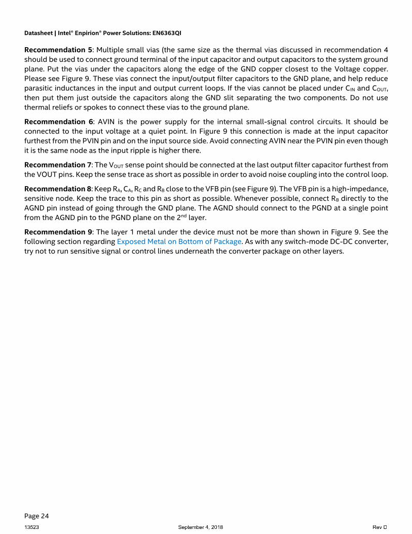
DESIGN CONSIDERATIONS FOR LEAD-FRAME BASED MODULES
Exposed Metal on Bottom of Package
Lead-frames offer many advantages in thermal performance such as in reduced electrical lead resistance and
in overall footprint; however, they do require some special considerations.
In the assembly process lead frame construction requires some of the lead-frame cantilevers be exposed at
the point where wire-bond or internal passives are attached for mechanical support. This results in several
small pads being exposed on the bottom of the package, as shown in Figure 10.
Only the thermal pad and the perimeter pads are to be mechanically or electrically connected to the board.
The PCB top layer under the EN6363QI should be clear of any metal (copper pours, traces, or vias) except for
the thermal pad. The “shaded-out” area in Figure 10 represents the area that should be clear of any metal on
the top layer of the PCB. Any layer 1 metal under the shaded-out area runs the risk of undesirable shorted
connections even if it is covered by solder mask.
The solder stencil aperture should be smaller than the PCB ground pad. This will prevent excess solder from
causing bridging between adjacent pins or other exposed metal under the package. See Figure 11 for details.
Figure 10: Lead-Frame exposed metal (Bottom View)
Shaded area highlights exposed metal that is not to be mechanically or electrically connected to the PCB.
Datasheet | Intel® Enpirion® Power Solutions: EN6363QI
Page 26
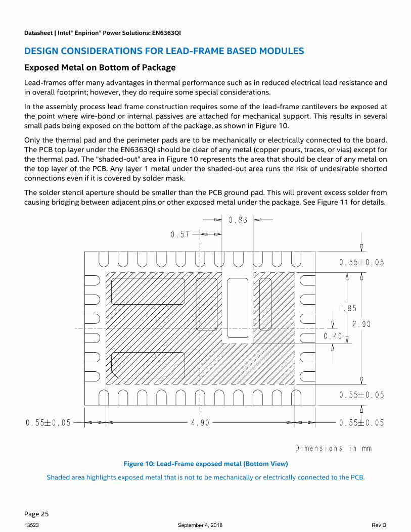
Figure 11: Landing Pattern with Solder Stencil (Top View)
The solder stencil aperture for the thermal PGND pad is shown in Figure 11 and is based on Enpirion power product
manufacturing specifications.
Datasheet | Intel® Enpirion® Power Solutions: EN6363QI
Page 27
PACKAGE DIMENSIONS
Figure 12: EN6363QI Package Dimensions
Packing and Marking Information: https://www.altera.com/support/quality-and-reliability/packing.html

Datasheet | Intel® Enpirion® Power Solutions: EN6363QI
WHERE TO GET MORE INFORMATION
For more information about Intel® and Enpirion® PowerSoCs, visit:
www.altera.com/enpirion
© 2017 Intel Corporation. All rights reserved. Intel, the Intel logo, Altera, ARRIA, CYCLONE, ENPIRION, MAX, MEGACORE, NIOS, QUARTUS, and STRATIX words and logos are trademarks of Intel
Corporation or its subsidiaries in the U.S. and/or other countries. Other marks and brands may be claimed as the property of others. Intel reserves the right to make changes to any products and
services at any time without notice. Intel assumes no responsibility or liability arising out of the application or use of any information, product, or service described herein except as expressly agreed to
in writing by Intel. Intel customers are advised to obtain the latest version of device specifications before relying on any published information and before placing orders for products or services.
* Other marks and brands may be claimed as the property of others.
Page 28
REVISION HISTORY
Rev Date Change(s)
A June, 2017 Initial Release
B Aug, 2017 Updated EMI Performance Curves on page 10 from 3m to 10m
C March, 2018 Updated minimum operating VOUT to 0.6V from 0.75V
D August, 2018 Updated RB value in Table 1 for 0.9V from 590k to 498k


![I:GG:HIG>6A :HH:CI>6A 8A>B6I: K6G>67A:H · I]Z YZh^\cVi^dch ZbeadnZY VcY i]Z egZhZciVi^dc d[ bViZg^Va ^c i]^h ^c[dgbVi^dc egdYjXi Yd cdi ^bean i]Z ZmegZhh^dc d[ Vcn de^c^dc l]VihdZkZg](https://img.pdfslide.us/doc/110x75/605b904e0bb48f292a0fe3d4/igghig6a-hhci6a-8ab6i-k6g67ah-iz-yzhcvidch-zbeadnzy-vcy.jpg)