Embed Size (px)
Citation preview
Product Specification
1 / 23
LB065WQ2Liquid Crystal Display
Ver.0.0 Jan. 26. 2004
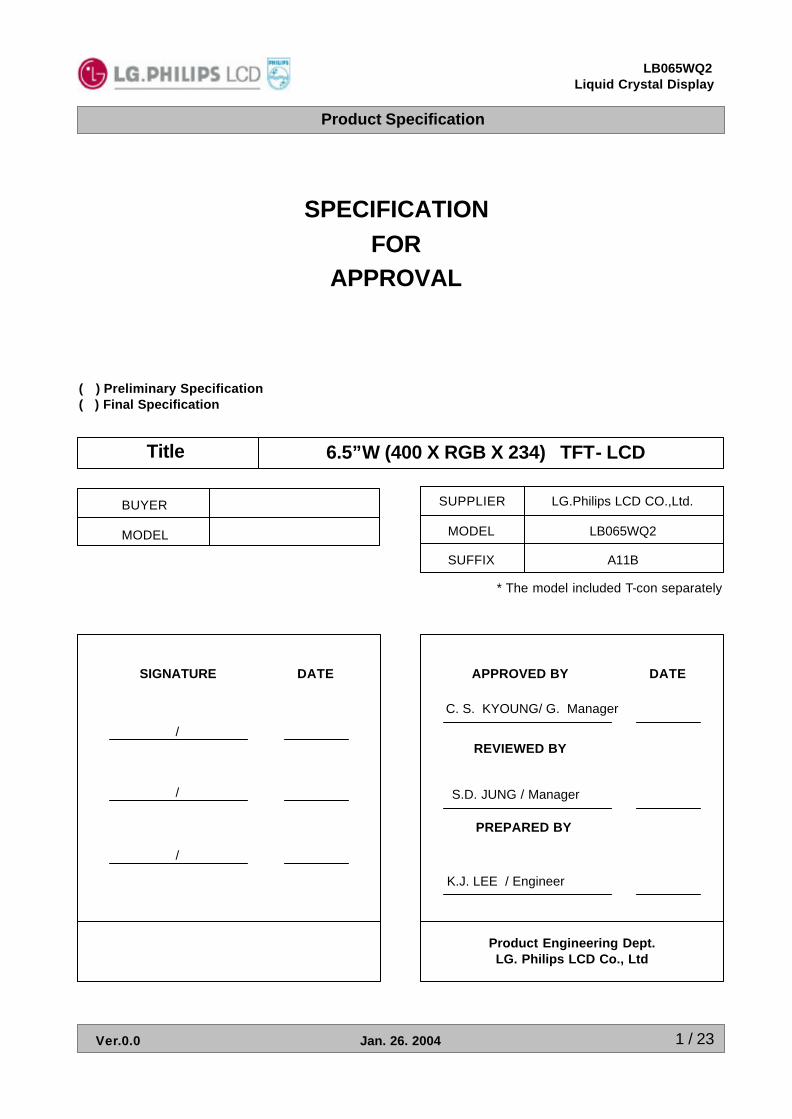
Title 6.5”W (400 X RGB X 234) TFT- LCD
BUYER
MODEL
SIGNATURE DATE
/
/
/
Product Engineering Dept.LG. Philips LCD Co., Ltd
APPROVED BY DATE
REVIEWED BY
PREPARED BY
A11BSUFFIX
LB065WQ2MODEL
LG.Philips LCD CO.,Ltd.SUPPLIER
SPECIFICATIONFOR
APPROVAL
() Preliminary Specification( ) Final Specification
C. S. KYOUNG/ G. Manager
S.D. JUNG / Manager
K.J. LEE / Engineer
* The model included T-con separately
Product Specification
2 / 23
LB065WQ2Liquid Crystal Display
Ver.0.0 Jan. 26. 2004
Contents
20International Standards11
22Precautions13
21Packing12
19Reliability Test10
17Mechanical Characteristics9
14Electro-optical Characteristics8
8Electrical Characteristics7
6Absolute Maximum Ratings6
5Interface (Input Terminal)5
4General Specification4
4Features3
4Summary2
3Record of Revisions1
PAGEITEMNO.
Product Specification
3 / 23
LB065WQ2Liquid Crystal Display
Ver.0.0 Jan. 26. 2004
RECORDS OF REVISIONS
First Draft(Preliminary)-Jan.26.20040.0
SummaryPageRevision
DateRevision No.
Product Specification
4 / 23
LB065WQ2Liquid Crystal Display
Ver.0.0 Jan. 26. 2004
1. Summary
3. General Specification
This module utilizes amorphous silicon thin film transistors and a 16:9 aspect ratio. A 6.5” active matrix liquid crystal display allows full color to be displayed.
The applications are Portable DVD, Multimedia applications and others AV system.
6.5”(16.39)Screen Size (Diagonal)
0.1195(W) [mm] X 0.3389(H) [mm] Dot Pitch
Anti-Glare TreatmentSurface Treatment
CCFL with 3 wave-length spectrum (L Type)Backlight
145g (TYP.)Weight
RGB vertical stripesColor Filter Array
400(W) X 3(RGB) X 234(H)Number Of dots
143.4[mm] X 79.3 [mm] TYP.Active Area
155.5[mm] X 89.8[mm] X 6.0 [mm] TYP.Outline Dimension (W x H x D)
TN Type Full Color / Transmitting Type
/ Normally White
Display Mode
a-Si TFT active matrixDisplay Technology
SPECIFICATIONCHARACTERISTIC ITEM
2. Features
•Utilizes a panel with a 16:9 aspect ratio, which makes the module suitable for use in wide-screen systems.
•The 6.5”screen produces a high resolution image that is composed of 93,600 pixel elements in a stripearrangement.
•Wide viewing angle technology is employed. [The most suitable viewing direction is in the 6 o’clock direction.]
•By adopting an active matrix drive, a picture with high contrast is realized.•A thin, light and compact module is accomplished through the use of COG mounting technology.•By adopting a high aperture panel, high transmittance color filter and high transmission polarizing plates,
transmittance ratio is realized.•This module is compatible with the T-con(Timing controller) developed by LG.Philips LCD.
[ T-con Model Name : FORT_REV(HS503022) , Part Number :0IHYL -0047A ]For a application including the T-con, please refer to the T-con datasheet with this specification sheet.
Product Specification
5 / 23
LB065WQ2Liquid Crystal Display
Ver.0.0 Jan. 26. 2004
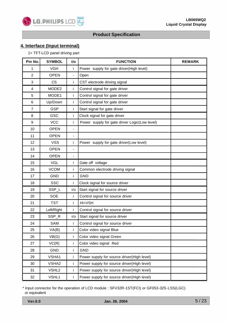
4. Interface (Input terminal)1> TFT-LCD panel driving part
Pin No. SYMBOL i/o FUNCTION REMARK
1 VGH i Power supply for gate driver(High level)
2 OPEN - Open
3 CS i CST electrode driving signal
4 MODE2 i Control signal for gate driver
5 MODE1 i Control signal for gate driver
6 Up/Down i Control signal for gate driver
7 GSP i Start signal for gate driver
8 GSC i Clock signal for gate driver
9 VCC i Power supply for gate driver Logic(Low level)
10 OPEN -
11 OPEN -
12 VSS i Power supply for gate driver(Low level)
13 OPEN -
14 OPEN -
15 VGL i Gate off voltage
16 VCOM i Common electrode driving signal
17 GND i GND
18 SSC i Clock signal for source driver
19 SSP_L i/o Start signal for source driver
20 SOE i Control signal for source driver
21 TST i Hi=VSH
22 Left/Right i Control signal for source driver
23 SSP_R i/o Start signal for source driver
24 SAM i Control signal for source driver
25 VA(B) i Color video signal Blue
26 VB(G) i Color video signal Green
27 VC(R) i Color video signal Red
28 GND i GND
29 VSHA1 i Power supply for source driver(High level)
30 VSHA2 i Power supply for source driver(High level)
31 VSHL2 i Power supply for source driver(High level)
32 VSHL1 i Power supply for source driver(High level)
* Input connector for the operation of LCD module : SFV32R-1ST(FCI) or GF053-32S-LSS(LGC) or equivalent
Product Specification
6 / 23
LB065WQ2Liquid Crystal Display
Ver.0.0 Jan. 26. 2004
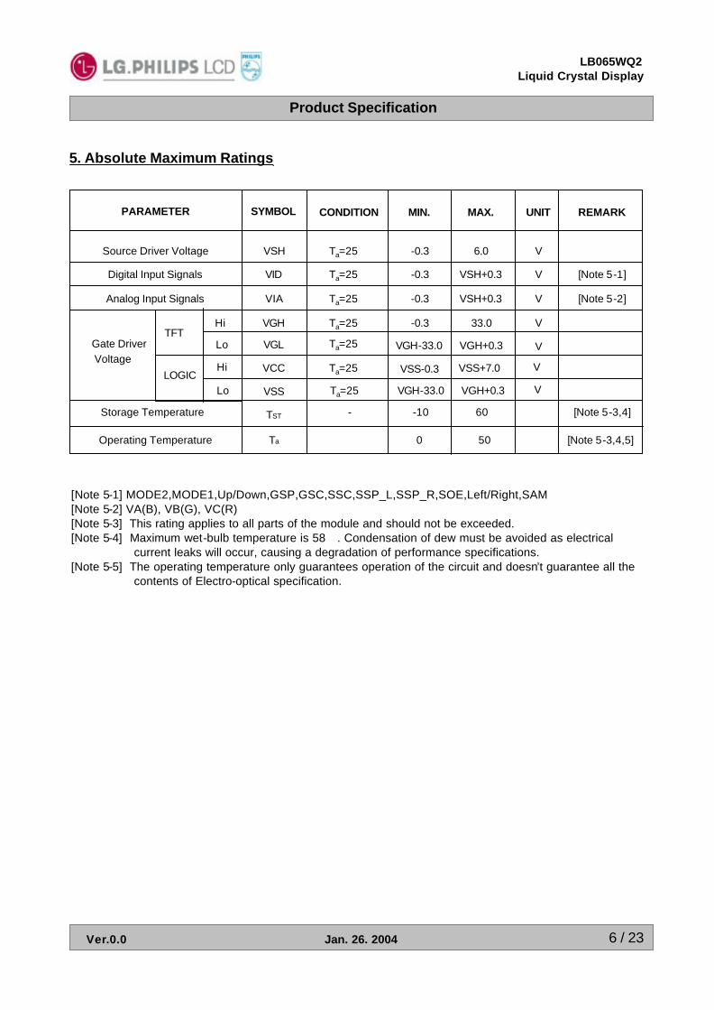
5. Absolute Maximum Ratings
[Note 5-1] MODE2,MODE1,Up/Down,GSP,GSC,SSC,SSP_L,SSP_R,SOE,Left/Right,SAM[Note 5-2] VA(B), VB(G), VC(R)[Note 5-3] This rating applies to all parts of the module and should not be exceeded.[Note 5-4] Maximum wet-bulb temperature is 58. Condensation of dew must be avoided as electrical
current leaks will occur, causing a degradation of performance specifications.[Note 5-5] The operating temperature only guarantees operation of the circuit and doesn’t guarantee all the
contents of Electro-optical specification.
V
VSS+7.0VSS-0.3Ta=25
VGL VVGH-33.0Ta=25
VCC
V33.0-0.3Ta=25VGH
Gate DriverVoltage
[Note 5-2]VVSH+0.3-0.3Ta=25VIAAnalog Input Signals
[Note 5-1]VVSH+0.3-0.3Ta=25VIDDigital Input Signals
V6.0-0.3Ta=25VSHSource Driver Voltage
REMARKUNITMAX.MIN.CONDITIONSYMBOLPARAMETER
500 [Note 5-3,4,5]Operating Temperature
[Note 5-3,4]60-10-TSTStorage Temperature
TFT
LOGIC
Hi
Lo
Hi
Lo Ta=25VSS
VGH+0.3
V
VGH-33.0 VGH+0.3
Ta
Product Specification
7 / 23
LB065WQ2Liquid Crystal Display
Ver.0.0 Jan. 26. 2004
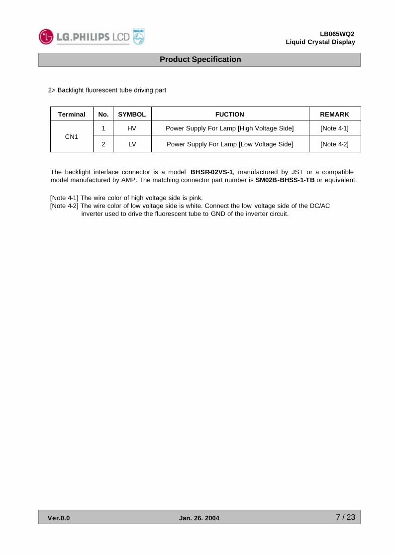
The backlight interface connector is a model BHSR-02VS-1, manufactured by JST or a compatible model manufactured by AMP. The matching connector part number is SM02B-BHSS-1-TB or equivalent.
[Note 4-1] The wire color of high voltage side is pink.[Note 4-2] The wire color of low voltage side is white. Connect the low voltage side of the DC/AC
inverter used to drive the fluorescent tube to GND of the inverter circuit.
2> Backlight fluorescent tube driving part
[Note 4-2]Power Supply For Lamp [Low Voltage Side]LV2
[Note 4-1]
REMARK
Power Supply For Lamp [High Voltage Side]HV1CN1
FUCTIONSYMBOLNo.Terminal
Product Specification
8 / 23
LB065WQ2Liquid Crystal Display
Ver.0.0 Jan. 26. 2004
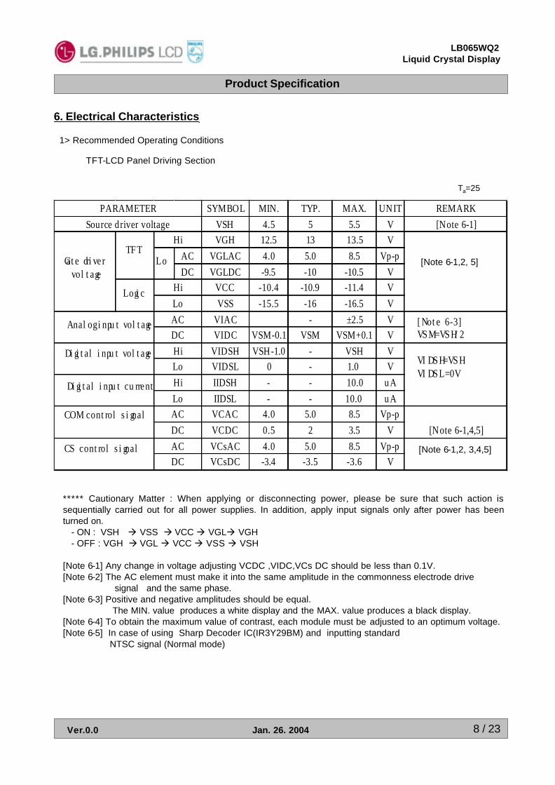
6. Electrical Characteristics
1> Recommended Operating Conditions
TFT-LCD Panel Driving Section
Ta=25
***** Cautionary Matter : When applying or disconnecting power, please be sure that such action is sequentially carried out for all power supplies. In addition, apply input signals only after power has been turned on.
- ON : VSH à VSS à VCC à VGLà VGH- OFF : VGH à VGL à VCC à VSS à VSH
[Note 6-1] Any change in voltage adjusting VCDC ,VIDC,VCs DC should be less than 0.1V.[Note 6-2] The AC element must make it into the same amplitude in the commonness electrode drive
signal and the same phase.[Note 6-3] Positive and negative amplitudes should be equal.
The MIN. value produces a white display and the MAX. value produces a black display.[Note 6-4] To obtain the maximum value of contrast, each module must be adjusted to an optimum voltage. [Note 6-5] In case of using Sharp Decoder IC(IR3Y29BM) and inputting standard
NTSC signal (Normal mode)
SYMBOL MIN. TYP. MAX. UNITVSH 4.5 5 5.5 VVGH 12.5 13 13.5 V
AC VGLAC 4.0 5.0 8.5 Vp-pDC VGLDC -9.5 -10 -10.5 V
VCC -10.4 -10.9 -11.4 VVSS -15.5 -16 -16.5 V
VIAC - ±2.5 VVIDC VSM-0.1 VSM VSM+0.1 V
VIDSH VSH-1.0 - VSH VVIDSL 0 - 1.0 VIIDSH - - 10.0 uAIIDSL - - 10.0 uAVCAC 4.0 5.0 8.5 Vp-pVCDC 0.5 2 3.5 VVCsAC 4.0 5.0 8.5 Vp-pVCsDC -3.4 -3.5 -3.6 V
AC
Hi
HiLo
DC
REMARK[Note 6-1]
PARAMETERSource driver voltage
HiLoHiLoACDCACDC
[Note 6-1,4,5]
Gate driver voltage
TFT
Logic
Lo
Analog input voltage
Digital input voltage
Digital input current
VIDSH=VSHVIDSL=0V
COM control signal
CS control signal
[Note 6-3]VSM=VSH/2
[Note 6-1,2, 3,4,5]
[Note 6-1,2, 5]
Product Specification
9 / 23
LB065WQ2Liquid Crystal Display
Ver.0.0 Jan. 26. 2004
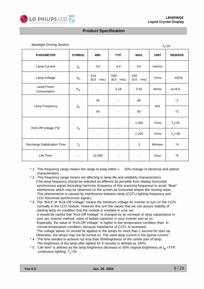
Backlight Driving Section Ta=25
*160-45
*4Minutes3--TSDischarge Stabilization Time
*5Hour--12,000-Life Time
Ta=-30Vrms1,200--
Ta=25Vrms1,000--
VSKick-Off Voltage (*3)
*2
kHz
80-45
fBLLamp Frequency
IBL=6.0Wrms3.503.18-PBLLamp PowerConsumption
±10[%]Vrms630(3.0rms)
530(6.0rms)
515(6.5rms)VBLLamp Voltage
mArms6.56.03.0IBLLamp Current
REMARKUNITMAX.TYP.MIN.SYMBOLPARAMETER
* 1 : This frequency range means the range to keep within ± 10% change of electrical and opticalcharacteristics.
* 2 : This frequency range means not affecting to lamp life and reliability characteristics.(The lamp frequency should be selected as different as possible from display horizontalsynchronous signal (Including harmonic frequency of this scanning frequency) to avoid “Beat”interference which may be observed on the screen as horizontal stripes like moving wave.This phenomenon is caused by interference between lamp (CCFL) lighting frequency andLCD horizontal synchronous signal.)
* 3 : The “MAX”of “Kick-Off Voltage”means the minimum voltage for inverter to turn on the CCFLnormally in the LCD module. However this isn’t the values that we can assure stability ofstarting lamp on condition that the module is installed in your set.It should be careful that “Kick-Off Voltage” is changed by an increase of stray capacitance in your set, inverter method, value of ballast capacitor in your inverter and so on.Especially, the value of “Kick-Off Voltage” is higher in low temperature condition than innormal temperature condition, because impedance of CCFL is increased.
"The voltage above Vs should be applied to the lamps for more than 1 second for start-up. Otherwise, the lamps may not be turned on. The used lamp current is the typical current."
* 4 : The time needed to achieve not less than 95%brightness of the center part of lamp. The brightness of the lamp after lighted for 5 minutes is defined as 100%.
* 5 : “Life time” is defined as the lamp brightness decrease to 50% original brightness at IBL=TYP;continuous lighting, Ta=25.
Product Specification
10 / 23
LB065WQ2Liquid Crystal Display
Ver.0.0 Jan. 26. 2004
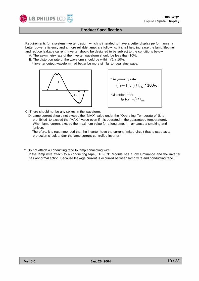
* Asymmetry rate:
( Ip – I –p |) / Irms * 100%
•Distortion rate:Ip (or I –p) / Irms
Requirements for a system inverter design, which is intended to have a better display performance, a better power efficiency and a more reliable lamp, are following. It shall help increase the lamp lifetimeand reduce leakage current. Inverter should be designed to be subject to the conditions below
A. The asymmetry rate of the inverter waveform should be less than 10%.B. The distortion rate of the waveform should be within √2 ± 10%.
* Inverter output waveform had better be more similar to ideal sine wave.
C. There should not be any spikes in the waveform.D. Lamp current should not exceed the “MAX” value under the “Operating Temperature”(it is
prohibited to exceed the “MAX.” value even if it is operated in the guaranteed temperature).When lamp current exceed the maximum value for a long time, it may cause a smoking andignition.Therefore, it is recommended that the inverter have the current limited circuit that is used as aprotection circuit and/or the lamp current-controlled inverter.
∗ Do not attach a conducting tape to lamp connecting wire.If the lamp wire attach to a conducting tape, TFT-LCD Module has a low luminance and the inverterhas abnormal action. Because leakage current is occurred between lamp wire and conducting tape.
I p
I -p
Product Specification
11 / 23
LB065WQ2Liquid Crystal Display
Ver.0.0 Jan. 26. 2004
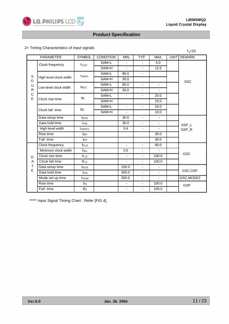
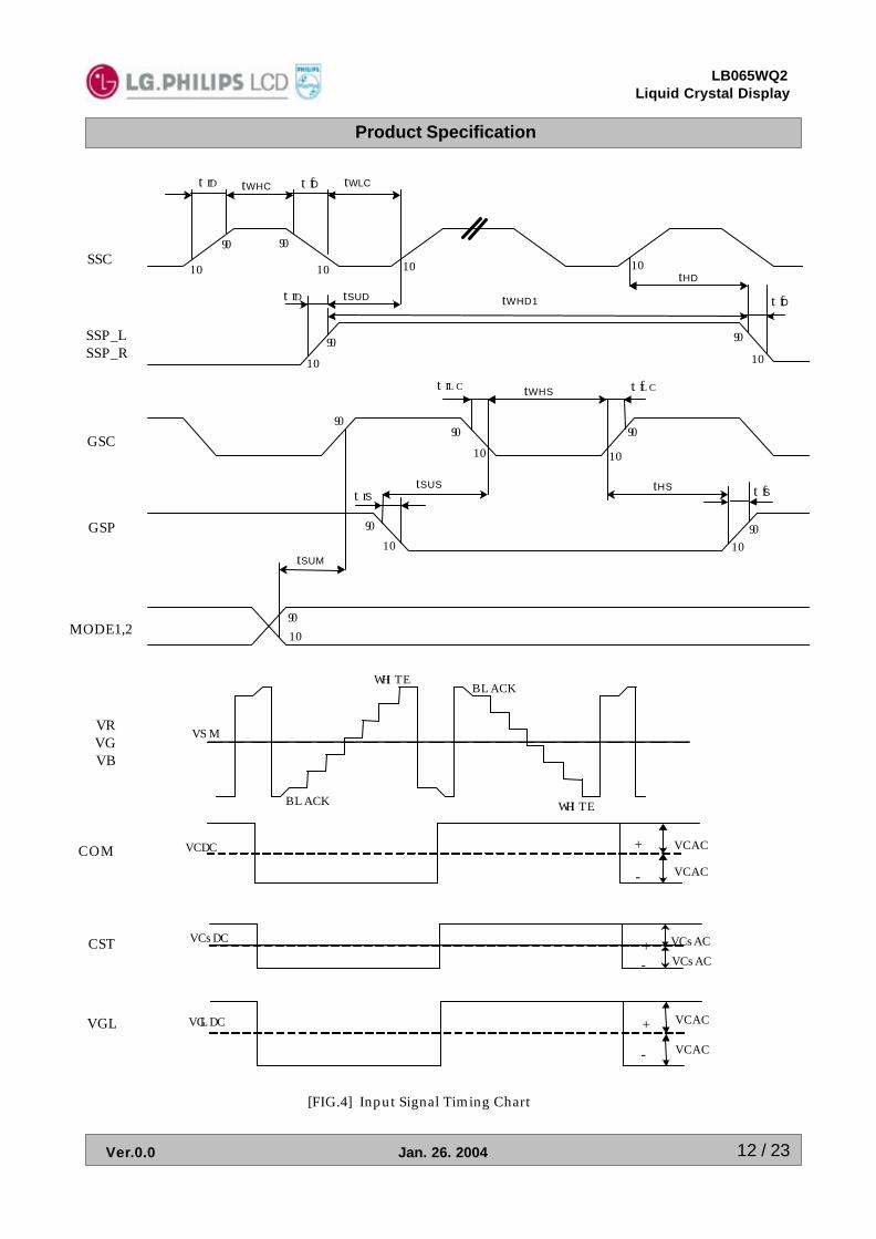
***** Input Signal Timing Chart : Refer [FIG.4].
2> Timing Characteristics of input signals
SYMBOL CONDITION MIN. TYP. MAX. UNIT REMARK
SAM=L - - 5.0
SAM=H - - 12.5
SAM=L 80.0 -
SAM=H 30.0
SAM=L 80.0 - -
SAM=H 30.0 - -
SAM=L - - 20.0
SAM=H 10.0
SAM=L - - 20.0
SAM=H - 10.0
Data setup time tSUD 30.0 - - Data hold time t HD 30.0 - - High level width t WHD1 0.4 - -
Rise time tRP 30.0 Fall time tFP 30.0 Clock frequency fCLS - - 80.0 Minimum clock width fWL 0.5 - - Clock rise time tr LC - - 100.0 Clock fall time tf LC - - 100.0 Data setup time tSUS 100.0 - - Data hold time tHS 300.0 - - Mode set up time tSUM 300.0 - - GSC,MODE2
Rise time trS - - 100.0 Fall time tfS - - 100.0
PARAMETER
Clock frequency f CLD
High level clock width t WHC
SSC
Low level clock width tWLC
Clock rise time trD
Clock fall time tfD
SSP_LSSP_R
SOURCE
GSC
GSC,GSP
GSP
GATE
Ta=25
Product Specification
12 / 23
LB065WQ2Liquid Crystal Display
Ver.0.0 Jan. 26. 2004
SSC
SSP_LSSP_R
GSC
GSP
MODE1,2
[FIG.4] Input Signal Timing Chart
trD tWHC tfD tWLC
10
90 90
10 10
10
90 90
10
10
9090
10 10
90
10
9090
10
10
90
tSUDtrD tWHD1
tHD
tfD
trLC tfLCtWHS
tSUStrS
tHS tfS
tSUM
VRVGVB
VSM
BLACK
WHITEBLACK
WHITE
COM VCDC +
-
VCAC
VCAC
VGL VGLDC VCAC
VCAC-
+
CST VCsDC VCsAC
VCsAC-+
Product Specification
13 / 23
LB065WQ2Liquid Crystal Display
Ver.0.0 Jan. 26. 2004
4> SOE Terminal (Control signal for source driver)
This is control signal of switching sample holder circuit. Please set the high or low levelsynchronizing with SSP signal during the period each horizontal line.
High level = VSH Low level = GND
5> MODE1,2 terminal (Control signal for gate driver)
They are the terminal switching output mode of gate driver.(Setting to VGL level by force)
MODE1 MODE2 Outputting mode
H H Normal mode(1 line writing)
L H Out of use
H L 2 line same time writing mode
L L No Outputting
High level = VSH Low level = GND6>SAM terminal (Control signal for source driver)
Used as input pin for setting the selecting of normal sampling operation or 3-point simultaneoussampling operation.For normal sampling operation (SAM=Hi), video signals are sampled in order1 LCD source driver output.For 3-point simultaneous sampling operation(SAM=Lo), video signals are sampled in ordersimultaneously 3 LCD drive outputs.
7>Current dissipations
SYMBOL CONDITION MIN. TYP. MAX. UNITCurrent for source driver H ISH - 35 60
H IGH - 0.1 1.0 L IGL - 0.1 1.0
ICC - 0.1 1.0 ISS - 0.1 1.0
PARAMETER
LogicCurrent for gate driver
VSH = 5.0VVGH = 13.0VVGLDC = -10.0VVCC = -10.9VVSS = -16.0V
In case of using exclusive timing control IC(LPL standard) and inputting standardNTSC signal (Normal mode)
Ta=25
3> Left/Right,Up/Down terminal (Signal For Reverse Scanning)
H(High Level) =VSH , L(Low Level)=GND
Right/Left & Up/Down Reverse Mode
Up/Down Reverse Mode
Left/Right Reverse Mode
Normal Mode
REMARKMODE Left/Right Up/Down
H
H H
H
L
LL
L
Refer to the p. 15 [Note 7-3].
Product Specification
14 / 23
LB065WQ2Liquid Crystal Display
Ver.0.0 Jan. 26. 2004
7. Electro-optical Characteristics
ms
ms
。
。
。
。
-
-
-
cd/m2
UNIT
4530-τdFall[Note 7-4]
2010-Θ=0。
τrRiseResponseTime
-6560Θdφ=270°
-5040Θuφ=90°
-6560Θrφ=0° [Note 7-2][Note 7-3]
-6560
CR≥5
Θlφ=180°
ViewingAngle
0.3590.3290.299Wy
[Note 7-1]0.343
IBL=6mArmsWxWhite Color
Chromaticity
[Note 7-2]-400150OptimalCRContrast Ratio
[Note 7-1]-400320IBL=6mArmsYLuminance
REMARKMAX.TYP.MIN.CONDITIONSYMBOLPARAMETER
Ta=25
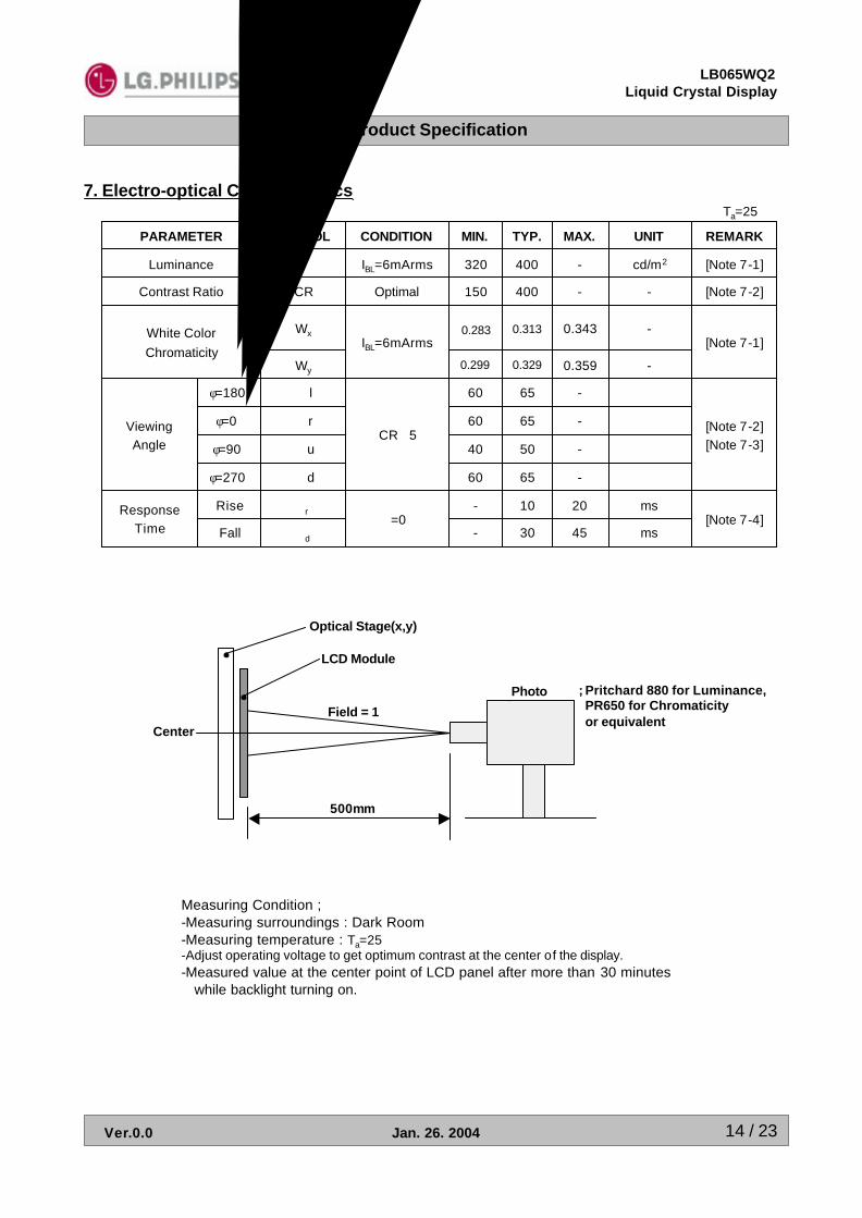
Photo detectorField = 1 °
Center
LCD Module
Optical Stage(x,y)
; Pritchard 880 for Luminance,PR650 for Chromaticity or equivalent
500mm
Measuring Condition ;-Measuring surroundings : Dark Room-Measuring temperature : Ta=25-Adjust operating voltage to get optimum contrast at the center of the display.-Measured value at the center point of LCD panel after more than 30 minutes
while backlight turning on.
0.3130.283
Product Specification
15 / 23
LB065WQ2Liquid Crystal Display
Ver.0.0 Jan. 26. 2004
[Note 7-1]
Measured on the center area of the panel by PHOTO RESEARCH photometer PR-880.
[Note 7-2]
Contrast ratio is defined as follows ;
Contrast Ratio(CR) =Photo detector output with LCD being “white”
Photo detector output with LCD being “black”
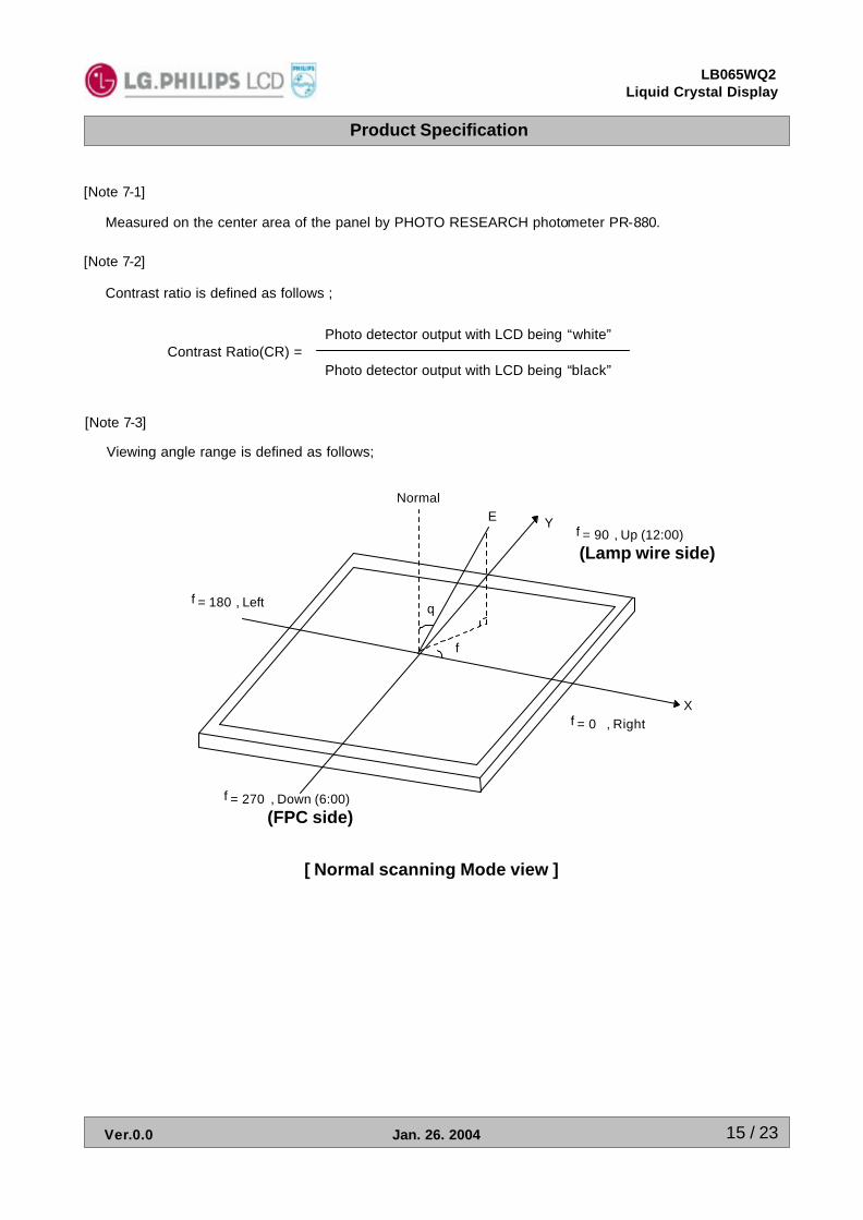
[Note 7-3]
Viewing angle range is defined as follows;
Normal
YE
f
q
f = 0 。, Right
f = 180。, Left
f = 270 。, Down (6:00)(FPC side)
f = 90 。, Up (12:00)(Lamp wire side)
X
[ Normal scanning Mode view ]
Product Specification
16 / 23
LB065WQ2Liquid Crystal Display
Ver.0.0 Jan. 26. 2004
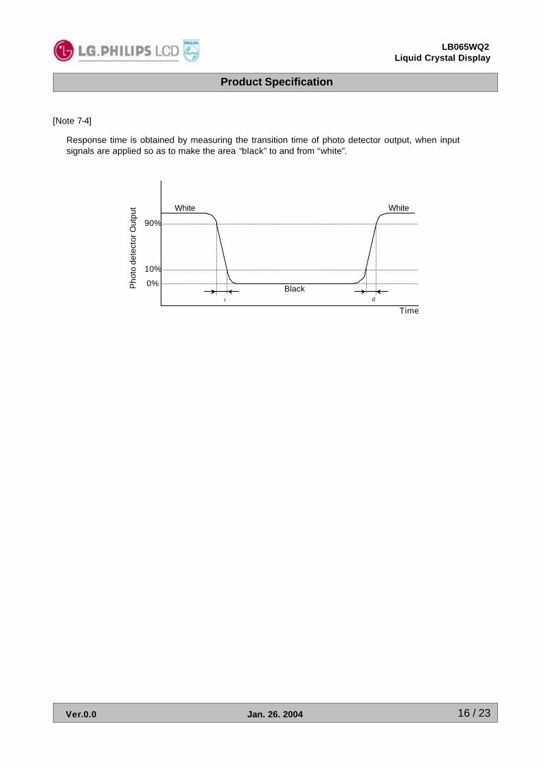
[Note 7-4]
Response time is obtained by measuring the transition time of photo detector output, when input signals are applied so as to make the area “black”to and from “white”.
0%
10%
90%
White White
Black
Time
Pho
to d
etec
tor O
utpu
t
τr τd
Product Specification
17 / 23
LB065WQ2Liquid Crystal Display
Ver.0.0 Jan. 26. 2004
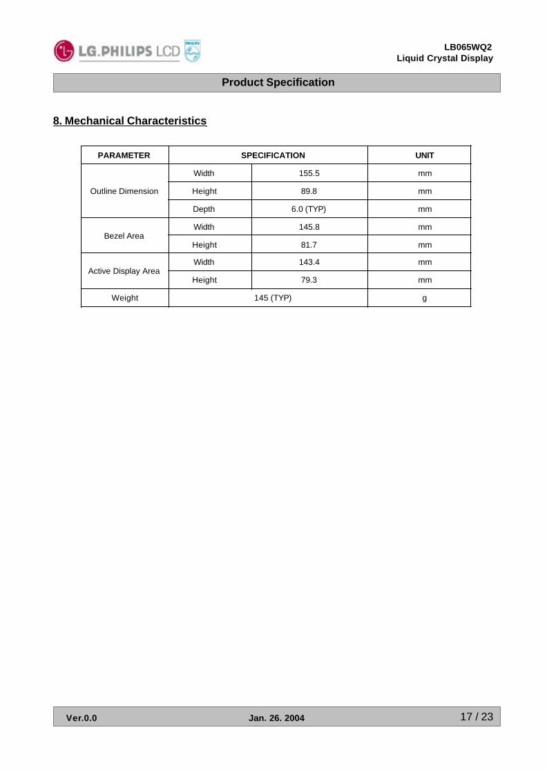
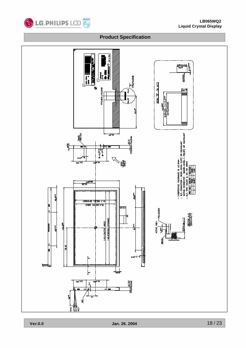
8. Mechanical Characteristics
145 (TYP)
79.3
143.4
81.7
145.8
6.0 (TYP)
89.8
155.5
gWeight
mmHeight
mmWidthActive Display Area
mmHeight
mmWidthBezel Area
mmDepth
mmHeight
mmWidth
Outline Dimension
UNITSPECIFICATIONPARAMETER
Product Specification
18 / 23
LB065WQ2Liquid Crystal Display
Ver.0.0 Jan. 26. 2004
Product Specification
19 / 23
LB065WQ2Liquid Crystal Display
Ver.0.0 Jan. 26. 2004
9. Reliability Test
***** Ta= Ambient Temperature
-10(0.5h) ~ 60(0.5h) / 100 cycles
Sine wave, 10 ~ 500 ~ 10Hz, 1.5G, 0.37oct/min3 axis, 1hour/axis
Half sine wave, 180G, 2msone shock of each six faces(I.e. run 180G 2ms for all six faces)
-Panel Surface/Top_Case: 150pF ±15kV 150Ω
(direct discharge, five times)-FPC input terminal : 100pF ±200V 0Ω
Ta=40 90%RH 240h
Ta=0 240h
Ta=50 240h
Ta=-10 240h
Ta=60 240h
Test Condition REMARK
High Temperature and High Humidity Operation Test5
Thermal Shock Test9
Vibration Test(non-operating)
8
Shock Test(non-operating)
7
Electro Static Discharge Test6
Low Temperature Operation Test4
High Temperature Operation Test3
Low Temperature Storage Test2
High Temperature Storage Test1
Test ItemsNo.
Product Specification
20 / 23
LB065WQ2Liquid Crystal Display
Ver.0.0 Jan. 26. 2004
10. International Standards
10-1. Safety
10-2. EMC
a) UL 60950, Third Edition, Underwriters Laboratories, Inc., Dated Dec. 11, 2000.Standard for Safety of Information Technology Equipment, Including Electrical Business Equipment.
b) CAN/CSA C22.2, No. 60950, Third Edition, Canadian Standards Association, Dec. 1, 2000.Standard for Safety of Information Technology Equipment, Including Electrical Business Equipment.
c) EN 60950 : 2000, Third EditionIEC 60950 : 1999, Third EditionEuropean Committee for Electro technical Standardization(CENELEC)EUROPEAN STANDARD for Safety of Information Technology Equipment Including Electrical BusinessEquipment.
a) ANSI C63.4 “Methods of Measurement of Radio-Noise Emissions from Low-Voltage Electrical and Electrical Equipment in the Range of 9kHZ to 40GHz. “American National Standards Institute(ANSI),1992
b) C.I.S.P.R “Limits and Methods of Measurement of Radio Interface Characteristics of InformationTechnology Equipment.“ International Special Committee on Radio Interference.
c) EN 55022 “Limits and Methods of Measurement of Radio Interface Characteristics of InformationTechnology Equipment.“European Committee for Electro technical Standardization.(CENELEC), 1998( Including A1: 2000 )
Product Specification
21 / 23
LB065WQ2Liquid Crystal Display
Ver.0.0 Jan. 26. 2004
11. Packing
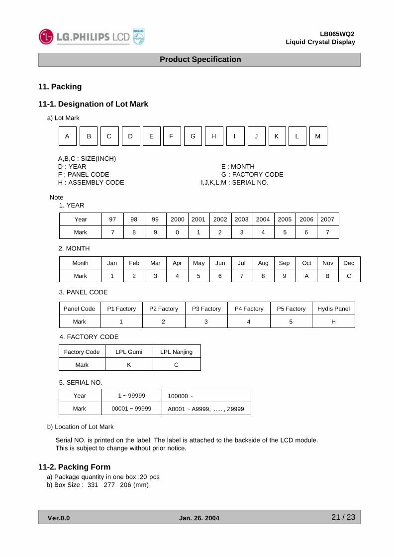
11-1. Designation of Lot Mark
11-2. Packing Forma) Package quantity in one box :20 pcsb) Box Size : 331×277×206 (mm)
a) Lot Mark
A B C D E F G H I J K L M
A,B,C : SIZE(INCH)D : YEAR E : MONTHF : PANEL CODE G : FACTORY CODEH : ASSEMBLY CODE I,J,K,L,M : SERIAL NO.
Note1. YEAR
b) Location of Lot Mark
2. MONTH
Serial NO. is printed on the label. The label is attached to the backside of the LCD module.This is subject to change without prior notice.
5. SERIAL NO.
Mark
Year
6
2006
2
2002
3
2003
4
2004
5
2005
0
2000
1
2001
7987
2007999897
B
Nov
Mark
Month
A
Oct
6
Jun
7
Jul
8
Aug
9
Sep
4
Apr
5
May
C321
DecMarFebJan
A0001 ~ A9999, ..... , Z999900001 ~ 99999Mark
100000 ~1 ~ 99999Year
4. FACTORY CODE
Mark
Factory Code
CK
LPL NanjingLPL Gumi
3. PANEL CODE
5
P5 Factory
4
P4 Factory
3
P3 Factory
H
Hydis Panel
2
P2 Factory
Mark
Panel Code
1
P1 Factory
Product Specification
22 / 23
LB065WQ2Liquid Crystal Display
Ver.0.0 Jan. 26. 2004
12. Precautions
Please pay attention to the following when you use this TFT LCD module.
12-1. Mounting Precautions
(1) You must mount a module using holes arranged in four corners or four sides.(2) You should consider the mounting structure so that uneven force(ex. Twisted stress) is not applied
to the module.And the case on which a module is mounted should have sufficient strength so that external forceis not transmitted directly to the module.
(3) Please attach a transparent protective plate to the surface in order to protect the polarizer.Transparent protective plate should have sufficient strength in order to the resist external force.
(4) You should adopt radiation structure to satisfy the temperature specification.(5) Acetic acid type and chlorine type materials for the cover case are not desirable because the former
generates corrosive gas of attacking the polarizer at high temperature and the latter causes circuitbreak by electro-chemical reaction.
(6) Do not touch, push or rub the exposed polarizers with glass, tweezers or anything harder than HBpencil lead. And please do not rub with dust clothes with chemical treatment.Do not touch the surface of polarizer for bare hand or greasy cloth.(Some cosmetics deterioratethe polarizer.)
(7) When the surface becomes dusty, please wipe gently with absorbent cotton or other soft materialslike chamois soaks with petroleum benzine. Normal-hexane is recommended for cleaning theadhesives used to attach front / rear polarizers. Do not use acetone, toluene and alcohol becausethey cause chemical damage to the polarizer.
(8) Wipe off saliva or water drops as soon as possible. Their long time contact with polarizer causesdeformations and color fading.
(9) Do not open the case because inside circuits do not have sufficient strength. (10) The metal case of a module should be contacted to electrical ground of your system.
12-2. Operating Precautions
(1) The spike noise causes the mis-operation of circuits. It should be lower than following voltage :V=±200mV(Over and under shoot voltage)
(2) Response time depends on the temperature.(In lower temperature, it becomes longer.)(3) Brightness depends on the temperature. (In lower temperature, it becomes lower.)
And in lower temperature, response time(required time that brightness is stable after turned on)becomes longer.
(4) Be careful for condensation at sudden temperature change. Condensation makes damage topolarizer or electrical contacted parts. And after fading condensation, smear or spot will occur.
(5) When fixed patterns are displayed for a long time, remnant image is likely to occur.(6) Module has high frequency circuits. Sufficient suppression to the electromagnetic interference
shall be done by system manufacturers. Grounding and shielding methods may be important tominimized the interference.
Product Specification
23 / 23
LB065WQ2Liquid Crystal Display
Ver.0.0 Jan. 26. 2004
Since a module is composed of electronic circuits, it is not strong to electrostatic discharge. Make certainthat treatment persons are connected to ground through wrist band etc. And don’t touch interface pin directly.
12-3. Electrostatic Discharge Control
Strong light exposure causes degradation of polarizer and color filter.
12-4. Precautions For Strong Light Exposure
When storing modules as spares for a long time, the following precautions are necessary.(1) Store them in a dark place. Do not expose the module to sunlight or fluorescent light. Keep the
temperature between 5°C and 35°C at normal humidity.(2) The polarizer surface should not come in contact with any other object.
It is recommended that they be stored in the container in which they were shipped.
12-5. Storage
(1) When the protection film is peeled off, static electricity is generated between the film and polarizer.This should be peeled off slowly and carefully by people who are electrically grounded and with wellion-blown equipment or in such a condition, etc.
(2) The protection film is attached to the polarizer with a small amount of glue. If some stress is appliedto rub the protection film against the polarizer during the time you peel off the film, the glue is apt toremain on the polarizer.Please carefully peel off the protection film without rubbing it against the polarizer.
(3) When the module with protection film attached is stored for a long time, sometimes there remains avery small amount of glue still on the polarizer after the protection film is peeled off.
(4) You can remove the glue easily. When the glue remains on the polarizer surface or its vestige isrecognized, please wipe them off with absorbent cotton waste or other soft material like chamoissoaked with normal-hexane.
12-6. Handling Precautions For Protection Film


![TECHNICAL SPECIFICATION MODEL NO: ED029TC1 Product... · 20 P VSH Positive Source driving voltage 21 P VGH Positive Gate driving voltage ... TCON 0setting (TCON) 1 60h 0 1 # S2G[3:0],G2S[3:0]](https://img.pdfslide.us/doc/110x75/5b5df7ee7f8b9a51328b68e7/technical-specification-model-no-ed029tc1-product-20-p-vsh-positive-source.jpg)