Embed Size (px)
Citation preview
SOLOMON SYSTECH SEMICONDUCTOR TECHNICAL DATA
This document contains information on a new product. Specifications and information herein are subject to change without notice. http://www.solomon-systech.com SSD1328 Rev 1.4 P 1/39 April 2005 Copyright 2005 Solomon Systech Limited
SSD1328
Advance Information
128 x 128, 16 Gray Scale Dot Matrix OLED/PLED Segment/Common Driver with Controller
Solomon Systech April 2005 P 2/39 Rev 1.4 SSD1328
Table of content
GENERAL DESCRIPTION........................................................................................................................... 6
FEATURES................................................................................................................................................... 6
ORDERING INFORMATION ........................................................................................................................ 6
BLOCK DIAGRAM ....................................................................................................................................... 7
SSD1328Z GOLD BUMP DIE PAD ASSIGNMENT..................................................................................... 8 SSD1328Z DIE PAD COORDINATES............................................................................................................. 9 SSD1328Z DIE TRAY DIMENSIONS ..................................................................................................... 10
PIN DESCRIPTION..................................................................................................................................... 11 M, DOF# .................................................................................................................................................. 11 CL ............................................................................................................................................................ 11 M/S# ........................................................................................................................................................ 11 CLS.......................................................................................................................................................... 11 BS0, BS1, BS2 ........................................................................................................................................ 11 CS#.......................................................................................................................................................... 11 RES# ....................................................................................................................................................... 11 D/C#......................................................................................................................................................... 11 R/W#(WR#) ............................................................................................................................................. 12 E (RD#).................................................................................................................................................... 12 D7-D0........................................................................................................................................................ 12 VDD ........................................................................................................................................................... 12 VSS ........................................................................................................................................................... 12 VCC ........................................................................................................................................................... 12 VREF.......................................................................................................................................................... 12 IREF ........................................................................................................................................................... 12 VCOMH ....................................................................................................................................................... 12 VDDB....................................................................................................................................................... 12 VSSB ....................................................................................................................................................... 12 GDR......................................................................................................................................................... 13 RESE....................................................................................................................................................... 13 VBREF ....................................................................................................................................................... 13 FB ............................................................................................................................................................ 13 BGGND.................................................................................................................................................... 13 COM0-COM127....................................................................................................................................... 13 SEG0-SEG127 ........................................................................................................................................ 13
FUNCTIONAL BLOCK DESCRIPTIONS................................................................................................... 14 COMMAND DECODER ................................................................................................................................. 14 MPU PARALLEL 6800-SERIES INTERFACE................................................................................................... 14 MPU PARALLEL 8080-SERIES INTERFACE................................................................................................... 14 MPU SERIAL INTERFACE............................................................................................................................ 14 OSCILLATOR CIRCUIT AND DISPLAY TIME GENERATOR ................................................................................ 16 CURRENT CONTROL AND VOLTAGE CONTROL ............................................................................................. 16 SEGMENT DRIVERS/COMMON DRIVERS....................................................................................................... 16 GRAPHIC DISPLAY DATA RAM (GDDRAM) ................................................................................................ 16 GRAPHIC DISPLAY DATA RAM (GDDRAM) ADDRESS MAP......................................................................... 16 GRAY SCALE DECODER ............................................................................................................................. 19
COMMAND TABLE .................................................................................................................................... 20
SSD1328 Rev 1.4 P 3/39 April 2005 Solomon Systech
COMMAND DESCRIPTIONS..................................................................................................................... 23 SET COLUMN ADDRESS.............................................................................................................................. 23 SET ROW ADDRESS ................................................................................................................................... 23 SET CONTRAST CONTROL REGISTER.......................................................................................................... 23 SET CURRENT RANGE................................................................................................................................ 23 SET RE-MAP.............................................................................................................................................. 24 SET DISPLAY START LINE........................................................................................................................... 24 SET DISPLAY OFFSET ................................................................................................................................ 24 SET DISPLAY MODE ................................................................................................................................... 25 SET MULTIPLEX RATIO ...............................................................................................................................25 SET DISPLAY ON/OFF ................................................................................................................................ 25 SET PHASE LENGTH................................................................................................................................... 25 SET ROW PERIOD...................................................................................................................................... 25 SET DISPLAY CLOCK DIVIDE RATIO............................................................................................................. 26 SET OSCILLATOR FREQUENCY.................................................................................................................... 26 SET GRAY SCALE TABLE............................................................................................................................ 26 NOP......................................................................................................................................................... 26 STATUS REGISTER READ............................................................................................................................ 26
MAXIMUM RATINGS ................................................................................................................................. 27
DC CHARACTERISTICS............................................................................................................................ 27
AC CHARACTERISTICS............................................................................................................................ 28
APPLICATION EXAMPLE ......................................................................................................................... 32
SSD1328TR1 TAB PACKAGE DIMENSION............................................................................................. 33 SSD1328TR1 PIN ASSIGNMENT .......................................................................................................... 35
APPENDIX.................................................................................................................................................. 37 INTERNAL DC-DC VOLTAGE CONVERTER APPLICATION CIRCUIT.................................................................. 37 VDDB....................................................................................................................................................... 37 VSSB ....................................................................................................................................................... 37 GDR......................................................................................................................................................... 37 RESE....................................................................................................................................................... 37 VBREF ....................................................................................................................................................... 37 FB ............................................................................................................................................................ 37 SET DC-DC CONVERTER COMMAND.......................................................................................................... 38
Solomon Systech April 2005 P 4/39 Rev 1.4 SSD1328
TABLE OF TABLES Table 1 - SSD1328Z Gold bump die pad coordinates .................................................................................. 9 Table 2 - MCU interface setting .................................................................................................................. 11 Table 3 - GDDRAM Address Map - Horizontal Address Increment A[2]=0, Column Address Re-map
A[0]=0, Nibble Re-map A[1]=0, COM Re-map A[4]=0, Display Start Line=00H (Data byte sequence: D0, D1, D2 … D8191).......................................................................................................................... 16
Table 4 - GDDRAM Address Map - Vertical Address Increment A[2]=1, Column Address Re-map A[0]=0, Nibble Re-map A[1]=0, COM Re-map A[4]=0, Display Start Line=00H (Data byte sequence: D0, D1, D2 … D8191) ....................................................................................................................................... 17
Table 5 - GDDRAM Address Map - Horizontal Address Increment A[2]=0, Column Address Re-map A[0]=1, Nibble Re-map A[1]=1, COM Re-map A[4]=0, Display Start line=00H (Data byte sequence: D0, D1, D2 … D8191).......................................................................................................................... 17
Table 6 - GDDRAM Address Map - Horizontal Address Increment A[2]=0, Column Address Re-map A[0]=0, Nibble Re-map A[1]=0, COM Re-map A[4]=1, Display Start Line=78H (Data byte sequence: D0, D1, D2 … D8191).......................................................................................................................... 18
Table 7 - GDDRAM Address Map - Horizontal Address Increment A[2]=0, Column Address Re-map A[0]=0, Nibble Re-map A[1]=0, COM Re-map A[4]=0, Display Start Line=00H (Data byte sequence: D0, D1, D2 … D7811), Column Start Address = 01H, Column End Address = 3EH, Row Start Address = 01H, Row End Address = 7EH........................................................................................... 18
Table 8 -gray scale pulse width set table.................................................................................................... 19 Table 9 - Gray scale pulse width default values ......................................................................................... 19 Table 10 - Command Table (D/C# =0, R/W#(WR#)=0, E (RD#)=1)........................................................... 20 Table 11 - Read Command Table (D/C#=0, R/W#(WR#)=1, E(RD#)=1 for 6800 or E(RD#)=0 for 8080) .22 Table 12 - Address Increment Table (Automatic) ....................................................................................... 22 Table 13 - COM Re-map setting ................................................................................................................. 24 Table 14 - Mapping of data with each gray scale level at different display mode ...................................... 25 Table 15 - Maximum Ratings (Voltage Reference to VSS) .......................................................................... 27 Table 16 - DC Characteristics (Unless otherwise specified, Voltage Referenced to VSS, VDD = 2.4 to 3.5V,
TA = 25°C) ............................................................................................................................................ 27 Table 17 - AC Characteristics (Unless otherwise specified, Voltage Referenced to VSS, VDD = 2.4 to 3.5V,
TA = 25°C.) ........................................................................................................................................... 28 Table 18 - 6800-Series MPU Parallel Interface Timing Characteristics (VDD - VSS = 2.4 to 3.5V, TA = 25°C)
............................................................................................................................................................. 29 Table 19 - 8080-Series MPU Parallel Interface Timing Characteristics (VDD - VSS = 2.4 to 3.5V, TA = 25°C)
............................................................................................................................................................. 30 Table 20 - Serial Interface Timing Characteristics (VDD - VSS = 2.4 to 3.5V, TA = 25°C) ............................ 31 Table 21 - SSD1328TR1 pin assignment ................................................................................................... 36 Table 22- Component lists for internal DC-DC converter application ......................................................... 38
SSD1328 Rev 1.4 P 5/39 April 2005 Solomon Systech
TABLE OF FIGURES Figure 1 - Block Diagram .............................................................................................................................. 7 Figure 2 - SSD1328Z Gold bump die pad assignment ................................................................................. 8 Figure 3 - Display Data Read Back Procedure - Insertion of Dummy Read............................................... 14 Figure 4 - Display data write procedure in SPI mode ................................................................................. 15 Figure 5 - Oscillator Circuit.......................................................................................................................... 16 Figure 6 - Gray scale pulse width set diagram............................................................................................ 19 Figure 7 - Segment current vs Contrast setting .......................................................................................... 23 Figure 8 - 6800-series MPU Parallel Interface Characteristics................................................................... 29 Figure 9 - 8080-series MPU Parallel Interface Characteristics................................................................... 30 Figure 10 - Serial Interface Characteristics................................................................................................. 31 Figure 11 - Application Example for SSD1328TR1..................................................................................... 32 Figure 12 - SSD1328TR1 TAB pin assignment (Copper view, Mirror TAB design) ................................... 35
Solomon Systech April 2005 P 6/39 Rev 1.4 SSD1328
GENERAL DESCRIPTION SSD1328 is a single-chip CMOS OLED/PLED driver with controller for organic/polymer light
emitting diode dot-matrix graphic display system. SSD1328 consists of 256 high voltage/current driving output pins for driving 128 segments and 128 commons. This IC is designed for Common Cathode type OLED/PLED panel.
SSD1328 displays data directly from its internal 128x128x4 bits Graphic Display Data RAM
(GDDRAM). Data/Commands are sent from general MCU through the hardware selectable 6800-/8080-series compatible Parallel Interface or Serial Peripheral Interface.
SSD1328 has a 128-step contrast control and a 16 gray level control. The embedded on-chip
oscillator reduces the number of external components.
FEATURES ! Support max. 128 x 128 matrix panel ! Power supply: VDD=2.4V - 3.5V, VCC=8.0V - 18.0V ! OLED driving output voltage, 16V maximum ! Segment maximum source current: 300uA ! Common maximum sink current: 40mA ! Embedded 128 x 128 x 4 bit SRAM display buffer ! External current reference ! 128 step contrast control on monochrome passive OLED panel ! 16 gray scale ! On-Chip Oscillator ! Programmable Frame Rate/Pre-charge voltage ! 8-bit 6800-series Parallel Interface, 8-bit 8080-series Parallel Interface, Serial Peripheral
Interface. ! Row re-mapping and Column re-mapping ! Vertical scrolling ! Support Partial display ! Low power consumption (<5.0uA @sleep mode) ! Wide range of operating temperature: -30 to 90 °C
ORDERING INFORMATION
Ordering Part Number SEG COM Package Form Reference Remark
SSD1328Z 128 128 COG
Page 8
Die Size: 11.41mm x 1.63mm Die Thickness: 457 +/- 25um I/O pad pitch (a): 76.2um SEG pad pitch (b): 52.2um COM pad pitch (c): 51.8um
SSD1328TR1 128 128 TAB Page 33 --
SSD1328 Rev 1.4 P 7/39 April 2005
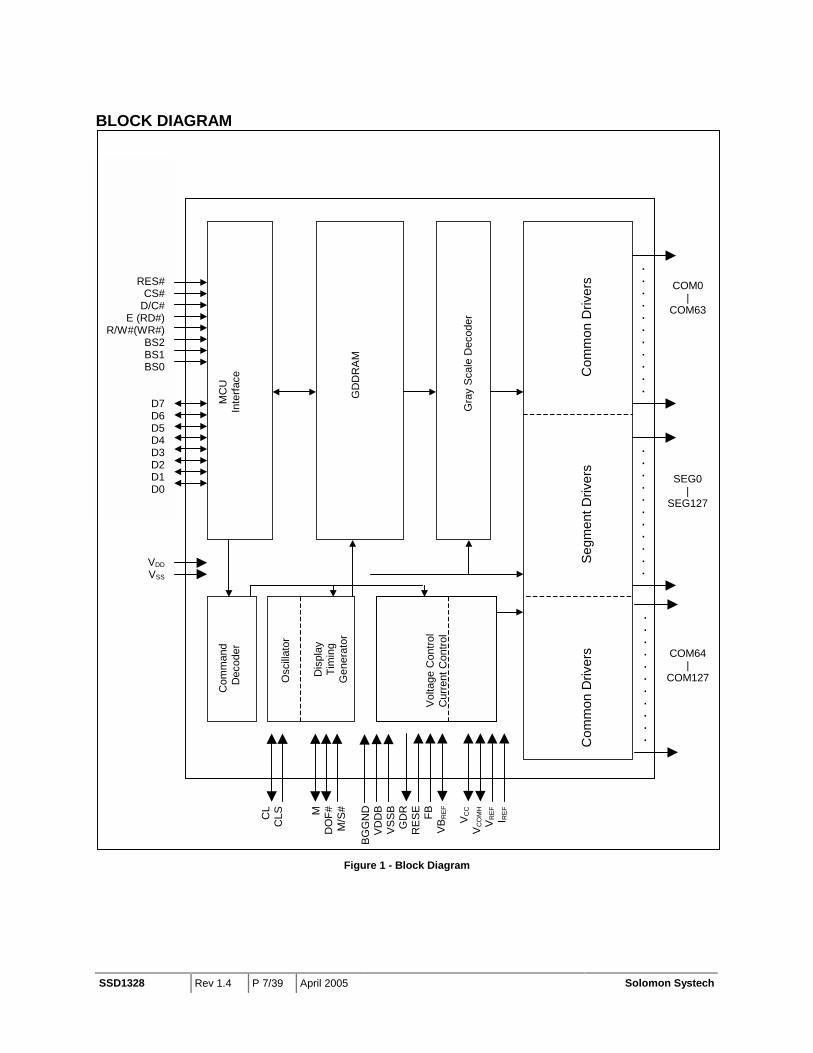
BLOCK DIAGRAM
Figure 1 -
BG
GN
DV
DD
B B R E B EF
Com
mon
Driv
ers
S
egm
ent D
river
s
Com
mon
Driv
ers
G
ray
Sca
le D
ecod
er
D
ispl
ay
Tim
ing
Gen
erat
or
O
scill
ator
G
DD
RA
M
MC
U
Inte
rface
RES#CS#
D/C#E (RD#)
R/W#(WR#)BS2BS1BS0
D7D6D5D4D3D2D1D0
Com
man
d D
ecod
er
VDDVSS
.
.
.
.
.
.
.
.
.
.
.
.
.
.
.
.
.
.
.
.
.
.
COM0 |
COM63
SEG0 |
SEG127
CL
CLS M
DO
F#M
/S#
COM64|
COM127
.
.
.
.
.
.
.
.
.
.
.
CC H EF
EF
Vol
tage
Con
trol
Cur
rent
Con
trol
Solomon Systech
Block Diagram
VS
SG
DR
ES F
VB
R VV
CO
M
VR I R
Solomon Systech April 2005 P 8/39 Rev 1.4 SSD1328
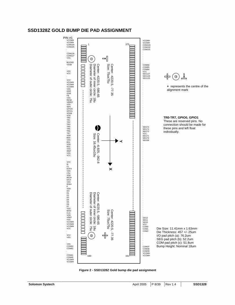
SSD1328Z GOLD BUMP DIE PAD ASSIGNMENT
Figure 2 - SSD1328Z Gold bump die pad assignment
VCOMH VCOMH COM104 COM105 . . COM126 COM127 VSS . BGGND VSSB . . VSS VCC . . VCC VCOMH VCOMH VCOMH VSS GDR GDR FB VSS RESE VBREF VSS SEN GPIO0 GPIO1 VDDB VDD TR0 TR1 TR2 TR3 TR4 TR5 TR6 TR7 VDD BS0 VSS BS1 VDD BS2 VSS IREF VSS VCC . . VCC M CL DOF# VSS CS# VDD RES# D/C# VSS R/W# E VDD DO D1 D2 D3 D4 D5 D6 D7 VSS M/S# CLS VDD VREF VSS VCOMH VCOMH VCOMH VCC . . VCC VSS . . VSS COM63 COM62 . . COM41 COM40 VCOMH VCOMH
VCOMH VCOMH COM103 COM102 COM101 . . . . . . COM66 COM65 COM64 VCC SEG127 SEG126 SEG125 . . . . . . . . . . . . . . . . . . . . . SEG74 SEG73 SEG72 VCC SEG71 SEG70 SEG69 . . . . . . . . . . . . . . . . . . . . . . . . . . . . . . . . . . SEG2 SEG1 SEG0 VCC COM0 COM1 COM2 . . . . . . COM37 COM38 COM39 VCOMH VCOMH
PIN #1
+ represents the centre of the alignment mark
Die Size: 11.41mm x 1.63mm Die Thickness: 457 +/- 25um I/O pad pitch (a): 76.2um SEG pad pitch (b): 52.2um COM pad pitch (c): 51.8um Bump Height: Nominal 18um
Center: -4220.5, -77.35
Size: 75ux75u
Center: -4220.5, -580.65
Diam
eter of inner circle: 18u D
iameter of outer circle: 75u
Center: -6.925, -362.6
Size: 16.45ux15u
Center: 4220.5, -580.65
Diam
eter of inner circle: 18u D
iameter of outer circle: 75u
Center: 4220.5, -77.35
Size: 75ux75u
X
Y
160
375 1
161
TR0-TR7, GPIO0, GPIO1These are reserved pins. No connection should be made for these pins and left float individually.
SSD1328 Rev 1.4 P 9/39 April 2005 Solomon Systech
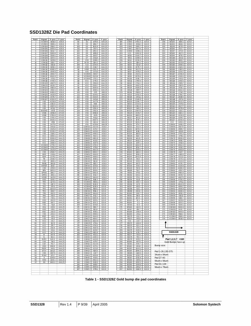
SSD1328Z Die Pad Coordinates
Table 1 - SSD1328Z Gold bump die pad coordinates
Pad # Signal X - p os Y - pos Pad # Signal X - p os Y - pos Pad # Signal X - p os Y - pos Pad # Signal X - p os Y - p os1 VCOM H -5619.9 -636.8 98 D1 1478.5 -644.25 198 COM 4 3703.3 624.8 298 SEG93 -1566.1 624.82 VCOM H -5568.1 -636.8 99 D2 1554.7 -644.25 199 COM 3 3651.5 624.8 299 SEG94 -1618.3 624.83 COM 104 -5516.3 -636.8 100 D2 1630.9 -644.25 200 COM 2 3599.7 624.8 300 SEG95 -1670.5 624.84 COM 105 -5464.5 -636.8 101 D3 1707.1 -644.25 201 COM 1 3547.9 624.8 301 SEG96 -1722.7 624.85 COM 106 -5412.7 -636.8 102 D4 1783.3 -644.25 202 COM 0 3496.1 624.8 302 SEG97 -1774.9 624.86 COM 107 -5360.9 -636.8 103 D5 1859.5 -644.25 203 VCC 3392.9 624.8 303 SEG98 -1827.1 624.87 COM 108 -5309.1 -636.8 104 D6 1935.7 -644.25 204 SEG0 3340.7 624.8 304 SEG99 -1879.3 624.88 COM 109 -5257.3 -636.8 105 D7 2011.9 -644.25 205 SEG1 3288.5 624.8 305 SEG100 -1931.5 624.89 COM 110 -5205.5 -636.8 106 VSS 2088.1 -644.25 206 SEG2 3236.3 624.8 306 SEG101 -1983.7 624.810 COM 111 -5153.7 -636.8 107 M /S# 2164.3 -644.25 207 SEG3 3184.1 624.8 307 SEG102 -2035.9 624.811 COM 112 -5101.9 -636.8 108 CLS 2240.5 -644.25 208 SEG4 3131.9 624.8 308 SEG103 -2088.1 624.812 COM 113 -5050.1 -636.8 109 VDD 2316.7 -644.25 209 SEG5 3079.7 624.8 309 SEG104 -2140.3 624.813 COM 114 -4998.3 -636.8 110 VREF 2397.3 -644.25 210 SEG6 3027.5 624.8 310 SEG105 -2192.5 624.814 COM 115 -4946.5 -636.8 111 VSS 2473.5 -644.25 211 SEG7 2975.3 624.8 311 SEG106 -2244.7 624.815 COM 116 -4894.7 -636.8 112 VCOM H 2549.7 -644.25 212 SEG8 2923.1 624.8 312 SEG107 -2296.9 624.816 COM 117 -4842.9 -636.8 113 VCOM H 2625.9 -644.25 213 SEG9 2870.9 624.8 313 SEG108 -2349.1 624.817 COM 118 -4791.1 -636.8 114 VCOM H 2702.1 -644.25 214 SEG10 2818.7 624.8 314 SEG109 -2401.3 624.818 COM 119 -4739.3 -636.8 115 VCC 2778.3 -644.25 215 SEG11 2766.5 624.8 315 SEG110 -2453.5 624.819 COM 120 -4687.5 -636.8 116 VCC 2854.5 -644.25 216 SEG12 2714.3 624.8 316 SEG111 -2505.7 624.820 COM 121 -4635.7 -636.8 117 VCC 2930.7 -644.25 217 SEG13 2662.1 624.8 317 SEG112 -2557.9 624.821 COM 122 -4583.9 -636.8 118 VCC 3006.9 -644.25 218 SEG14 2609.9 624.8 318 SEG113 -2610.1 624.822 COM 123 -4532.1 -636.8 119 VSS 3083.1 -644.25 219 SEG15 2557.7 624.8 319 SEG114 -2662.3 624.823 COM 124 -4480.3 -636.8 120 VSS 3173 -686.15 220 SEG16 2505.5 624.8 320 SEG115 -2714.5 624.824 COM 125 -4428.5 -636.8 121 VSS 3249.2 -686.15 221 SEG17 2453.3 624.8 321 SEG116 -2766.7 624.825 COM 126 -4376.7 -636.8 122 VSS 3325.4 -686.15 222 SEG18 2401.1 624.8 322 SEG117 -2818.9 624.826 COM 127 -4324.9 -636.8 123 VSS 3401.6 -686.15 223 SEG19 2348.9 624.8 323 SEG118 -2871.1 624.827 VSS -4239.8 -674.65 124 VSS 3477.8 -686.15 224 SEG20 2296.7 624.8 324 SEG119 -2923.3 624.828 VSS -4163.6 -674.65 125 VSS 3554 -686.15 225 SEG21 2244.5 624.8 325 SEG120 -2975.5 624.829 VSS -4087.4 -674.65 126 VSS 3630.2 -686.15 226 SEG22 2192.3 624.8 326 SEG121 -3027.7 624.830 VSS -4011.2 -674.65 127 VSS 3706.4 -686.15 227 SEG23 2140.1 624.8 327 SEG122 -3079.9 624.831 BGGND -3935 -674.65 128 VSS 3782.6 -686.15 228 SEG24 2087.9 624.8 328 SEG123 -3132.1 624.832 VSSB -3858.8 -674.65 129 VSS 3858.8 -686.15 229 SEG25 2035.7 624.8 329 SEG124 -3184.3 624.833 VSSB -3782.6 -674.65 130 VSS 3935 -686.15 230 SEG26 1983.5 624.8 330 SEG125 -3236.5 624.834 VSS -3706.4 -674.65 131 VSS 4011.2 -686.15 231 SEG27 1931.3 624.8 331 SEG126 -3288.7 624.835 VSS -3630.2 -674.65 132 VSS 4087.4 -686.15 232 SEG28 1879.1 624.8 332 SEG127 -3340.9 624.836 VSS -3554 -674.65 133 VSS 4163.6 -686.15 233 SEG29 1826.9 624.8 333 VCC -3393.1 624.837 VSS -3477.8 -674.65 134 VSS 4239.8 -686.15 234 SEG30 1774.7 624.8 334 COM 64 -3496.1 624.838 VSS -3401.6 -674.65 135 COM 63 4324.9 -636.8 235 SEG31 1722.5 624.8 335 COM 65 -3547.9 624.839 VSS -3325.4 -674.65 136 COM 62 4376.7 -636.8 236 SEG32 1670.3 624.8 336 COM 66 -3599.7 624.840 VSS -3249.2 -674.65 137 COM 61 4428.5 -636.8 237 SEG33 1618.1 624.8 337 COM 67 -3651.5 624.841 VSS -3159.3 -644.25 138 COM 60 4480.3 -636.8 238 SEG34 1565.9 624.8 338 COM 68 -3703.3 624.842 VCC -3083.1 -644.25 139 COM 59 4532.1 -636.8 239 SEG35 1513.7 624.8 339 COM 69 -3755.1 624.843 VCC -3006.9 -644.25 140 COM 58 4583.9 -636.8 240 SEG36 1461.5 624.8 340 COM 70 -3806.9 624.844 VCC -2930.7 -644.25 141 COM 57 4635.7 -636.8 241 SEG37 1409.3 624.8 341 COM 71 -3858.7 624.845 VCC -2854.5 -644.25 142 COM 56 4687.5 -636.8 242 SEG38 1357.1 624.8 342 COM 72 -3910.5 624.846 VCOM H -2778.3 -644.25 143 COM 55 4739.3 -636.8 243 SEG39 1304.9 624.8 343 COM 73 -3962.3 624.847 VCOM H -2702.1 -644.25 144 COM 54 4791.1 -636.8 244 SEG40 1252.7 624.8 344 COM 74 -4014.1 624.848 VCOM H -2625.9 -644.25 145 COM 53 4842.9 -636.8 245 SEG41 1200.5 624.8 345 COM 75 -4065.9 624.849 VSS -2549.7 -644.25 146 COM 52 4894.7 -636.8 246 SEG42 1148.3 624.8 346 COM 76 -4117.7 624.850 GDR -2451.4 -644.25 147 COM 51 4946.5 -636.8 247 SEG43 1096.1 624.8 347 COM 77 -4169.5 624.851 GDR -2375.2 -644.25 148 COM 50 4998.3 -636.8 248 SEG44 1043.9 624.8 348 COM 78 -4221.3 624.852 FB -2048.7 -644.25 149 COM 49 5050.1 -636.8 249 SEG45 991.7 624.8 349 COM 79 -4273.1 624.853 VSS -1968.1 -644.25 150 COM 48 5101.9 -636.8 250 SEG46 939.5 624.8 350 COM 80 -4324.9 624.854 RESE -1891.9 -644.25 151 COM 47 5153.7 -636.8 251 SEG47 887.3 624.8 351 COM 81 -4376.7 624.855 VBREF -1815.7 -644.25 152 COM 46 5205.5 -636.8 252 SEG48 835.1 624.8 352 COM 82 -4428.5 624.856 VSS -1739.5 -644.25 153 COM 45 5257.3 -636.8 253 SEG49 782.9 624.8 353 COM 83 -4480.3 624.857 SEN -1663.3 -644.25 154 COM 44 5309.1 -636.8 254 SEG50 730.7 624.8 354 COM 84 -4532.1 624.858 GPIO0 -1582.7 -644.25 155 COM 43 5360.9 -636.8 255 SEG51 678.5 624.8 355 COM 85 -4583.9 624.859 GPIO1 -1502.1 -644.25 156 COM 42 5412.7 -636.8 256 SEG52 626.3 624.8 356 COM 86 -4635.7 624.860 VDDB -1425.9 -644.25 157 COM 41 5464.5 -636.8 257 SEG53 574.1 624.8 357 COM 87 -4687.5 624.861 VDD -1349.7 -644.25 158 COM 40 5516.3 -636.8 258 SEG54 521.9 624.8 358 COM 88 -4739.3 624.862 TR0 -1273.5 -644.25 159 VCOM H 5568.1 -636.8 259 SEG55 469.7 624.8 359 COM 89 -4791.1 624.863 TR1 -1197.3 -644.25 160 VCOM H 5619.9 -636.8 260 SEG56 417.5 624.8 360 COM 90 -4842.9 624.864 TR2 -1121.1 -644.25 161 VCOM H 5619.9 624.8 261 SEG57 365.3 624.8 361 COM 91 -4894.7 624.865 TR3 -1044.9 -644.25 162 VCOM H 5568.1 624.8 262 SEG58 313.1 624.8 362 COM 92 -4946.5 624.866 TR4 -968.7 -644.25 163 COM 39 5516.3 624.8 263 SEG59 260.9 624.8 363 COM 93 -4998.3 624.867 TR5 -892.5 -644.25 164 COM 38 5464.5 624.8 264 SEG60 208.7 624.8 364 COM 94 -5050.1 624.868 TR6 -816.3 -644.25 165 COM 37 5412.7 624.8 265 SEG61 156.5 624.8 365 COM 95 -5101.9 624.869 TR7 -740.1 -644.25 166 COM 36 5360.9 624.8 266 SEG62 104.3 624.8 366 COM 96 -5153.7 624.870 VDD -663.9 -644.25 167 COM 35 5309.1 624.8 267 SEG63 52.1 624.8 367 COM 97 -5205.5 624.871 BS0 -587.7 -644.25 168 COM 34 5257.3 624.8 268 SEG64 -0.1 624.8 368 COM 98 -5257.3 624.872 VSS -511.5 -644.25 169 COM 33 5205.5 624.8 269 SEG65 -52.3 624.8 369 COM 99 -5309.1 624.873 BS1 -435.3 -644.25 170 COM 32 5153.7 624.8 270 SEG66 -104.5 624.8 370 COM 100 -5360.9 624.874 VDD -359.1 -644.25 171 COM 31 5101.9 624.8 271 SEG67 -156.7 624.8 371 COM 101 -5412.7 624.875 BS2 -282.9 -644.25 172 COM 30 5050.1 624.8 272 SEG68 -208.9 624.8 372 COM 102 -5464.5 624.876 VSS -202.3 -644.25 173 COM 29 4998.3 624.8 273 SEG69 -261.1 624.8 373 COM 103 -5516.3 624.877 IREF -126.1 -644.25 174 COM 28 4946.5 624.8 274 SEG70 -313.3 624.8 374 VCOM H -5568.1 624.878 VSS -49.9 -644.25 175 COM 27 4894.7 624.8 275 SEG71 -365.5 624.8 375 VCOM H -5619.9 624.879 VCC 26.3 -644.25 176 COM 26 4842.9 624.8 276 VCC -417.7 624.880 VCC 102.5 -644.25 177 COM 25 4791.1 624.8 277 SEG72 -469.9 624.881 VCC 178.7 -644.25 178 COM 24 4739.3 624.8 278 SEG73 -522.1 624.882 VCC 254.9 -644.25 179 COM 23 4687.5 624.8 279 SEG74 -574.3 624.883 VCC 331.1 -644.25 180 COM 22 4635.7 624.8 280 SEG75 -626.5 624.884 VCC 407.3 -644.25 181 COM 21 4583.9 624.8 281 SEG76 -678.7 624.885 M 487.9 -644.25 182 COM 20 4532.1 624.8 282 SEG77 -730.9 624.886 CL 564.1 -644.25 183 COM 19 4480.3 624.8 283 SEG78 -783.1 624.887 DOF# 640.3 -644.25 184 COM 18 4428.5 624.8 284 SEG79 -835.3 624.888 VSS 716.5 -644.25 185 COM 17 4376.7 624.8 285 SEG80 -887.5 624.889 CS# 792.7 -644.25 186 COM 16 4324.9 624.8 286 SEG81 -939.7 624.890 VDD 868.9 -644.25 187 COM 15 4273.1 624.8 287 SEG82 -991.9 624.891 RES# 945.1 -644.25 188 COM 14 4221.3 624.8 288 SEG83 -1044.1 624.892 D/C# 1021.3 -644.25 189 COM 13 4169.5 624.8 289 SEG84 -1096.3 624.893 VSS 1097.5 -644.25 190 COM 12 4117.7 624.8 290 SEG85 -1148.5 624.894 R/W# 1173.7 -644.25 191 COM 11 4065.9 624.8 291 SEG86 -1200.7 624.895 E 1249.9 -644.25 192 COM 10 4014.1 624.8 292 SEG87 -1252.9 624.896 VDD 1326.1 -644.25 193 COM 9 3962.3 624.8 293 SEG88 -1305.1 624.897 D0 1402.3 -644.25 194 COM 8 3910.5 624.8 294 SEG89 -1357.3 624.8
195 COM 7 3858.7 624.8 295 SEG90 -1409.5 624.8196 COM 6 3806.9 624.8 296 SEG91 -1461.7 624.8197 COM 5 3755.1 624.8 297 SEG92 -1513.9 624.8
Pad 1,2,3,? >160Gold Bumps face up
SSD1328
Bump size:
Pad 1-26,135-375:34um x 84umPad 27-40:56um x 56umPad 41-134:56um x 79um
Solomon Systech April 2005 P 10/39 Rev 1.4 SSD1328
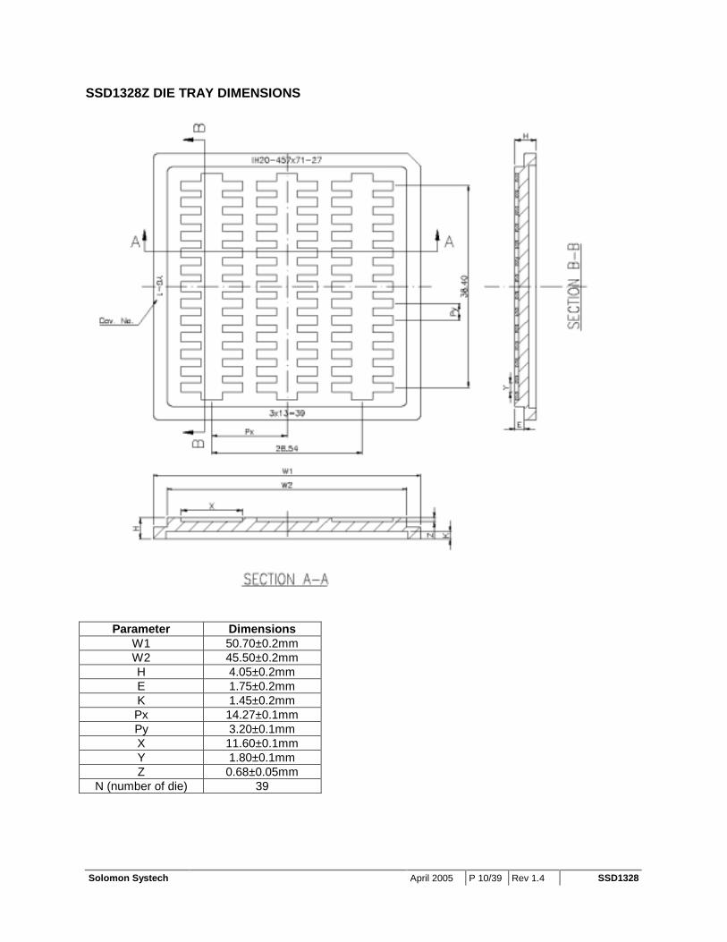
SSD1328Z DIE TRAY DIMENSIONS
Parameter Dimensions W1 50.70±0.2mm W2 45.50±0.2mm H 4.05±0.2mm E 1.75±0.2mm K 1.45±0.2mm Px 14.27±0.1mm Py 3.20±0.1mm X 11.60±0.1mm Y 1.80±0.1mm Z 0.68±0.05mm
N (number of die) 39
SSD1328 Rev 1.4 P 11/39 April 2005 Solomon Systech
PIN DESCRIPTION
M, DOF# These pins are No Connection pins. Nothing should be connected to these pins, nor they are connected together. These pins should be left open individually.
CL This pin is the system clock input. When internal clock is enabled, this pin should be left open. Nothing should be connected to this pin. In this case, the output clock frequency equals to the internal clock frequency. When internal oscillator is disabled, this pin receives display clock signal from external clock source.
M/S# This pin is an input pin and must be pulled high to enable the chip function.
CLS This pin is internal clock enable. When this pin is pulled high, internal clock is enabled. The internal clock will be disabled when it is pulled low, an external clock source must be connected to CL pin for normal operation.
BS0, BS1, BS2 These pins are MCU interface selection input. See the following table: 6800-parallel
interface 8080-parallel interface
Serial interface
BS0 0 0 0 BS1 0 1 0 BS2 1 1 0
Table 2 - MCU interface setting
CS# This pin is the chip select input. The chip is enabled for MCU communication only when CS# is pulled low.
RES# This pin is reset signal input. When the pin is low, initialization of the chip is executed.
D/C# This pin is Data/Command control pin. When the pin is pulled high, the input at D7-D0 is treated as display data. When the pin is pulled low, the input at D7-D0 will be transferred to the command register. For detail relationship to MCU interface signals, please refer to the Timing Characteristics Diagrams.
Solomon Systech April 2005 P 12/39 Rev 1.4 SSD1328
R/W#(WR#) This pin is MCU interface input. When interfacing to a 6800-series microprocessor, this pin will be used as Read/Write (R/W#) selection input. Pull this pin to “High” for read mode and pull it to “LOW” for write mode. When 8080 interface mode is selected, this pin will be the Write (WR#) input. Data write operation is initiated when this pin is pulled low and the CS# is pulled low.
E (RD#) This pin is MCU interface input. When interfacing to a 6800-series microprocessor, this pin will be used as the Enable (E) signal. Read/write operation is initiated when this pin is pulled high and the CS# is pulled low. When connecting to an 8080-microprocessor, this pin receives the Read (RD#) signal. Data read operation is initiated when this pin is pulled low and CS# is pulled low.
D7-D0 These pins are 8-bit bi-directional data bus to be connected to the microprocessor’s data bus. When serial mode is selected, D1 will be the serial data input SDIN and D0 will be the serial clock input SCLK.
VDD This is a voltage supply pin. It must be connected to external source.
VSS This is a ground pin. It also acts as a reference for the logic pins and the OLED driving voltages. It must be connected to external ground.
VCC This is the most positive voltage supply pin of the chip. It is supplied externally.
VREF This pin is the voltage reference for pre-charge voltage in driving OLED device. Voltage should be set to match with the OLED driving voltage in current drive phase. It can be either supplied externally or connected to VCC.
IREF This pin is segment current reference pin. A resistor should be connected between this pin and VSS. Set the current at 10uA. See setting in application example on page 32.
VCOMH This pin is the input pin for the voltage output high level for COM signals. A capacitor should be connected between this pin and VSS.
VDDB This is power pin. It should be connected to VDD.
VSSB This is ground pin. It must be connected to external ground.
SSD1328 Rev 1.4 P 13/39 April 2005 Solomon Systech
GDR This is used for testing purpose. It should be left open under normal operation.
RESE This is used for testing purpose. It should be left open under normal operation.
VBREF This is used for testing purpose. It should be left open under normal operation.
FB This is used for testing purpose. It should be left open under normal operation.
BGGND This is a ground pin for analog circuits. It must be connected to external ground.
COM0-COM127 These pins provide the Common switch signals to the OLED panel. These pins are in high impedance state when display is off.
SEG0-SEG127 These pins provide the OLED segment driving signals. These pins are in high impedance state when display is off.
Solomon Systech April 2005 P 14/39 Rev 1.4 SSD1328
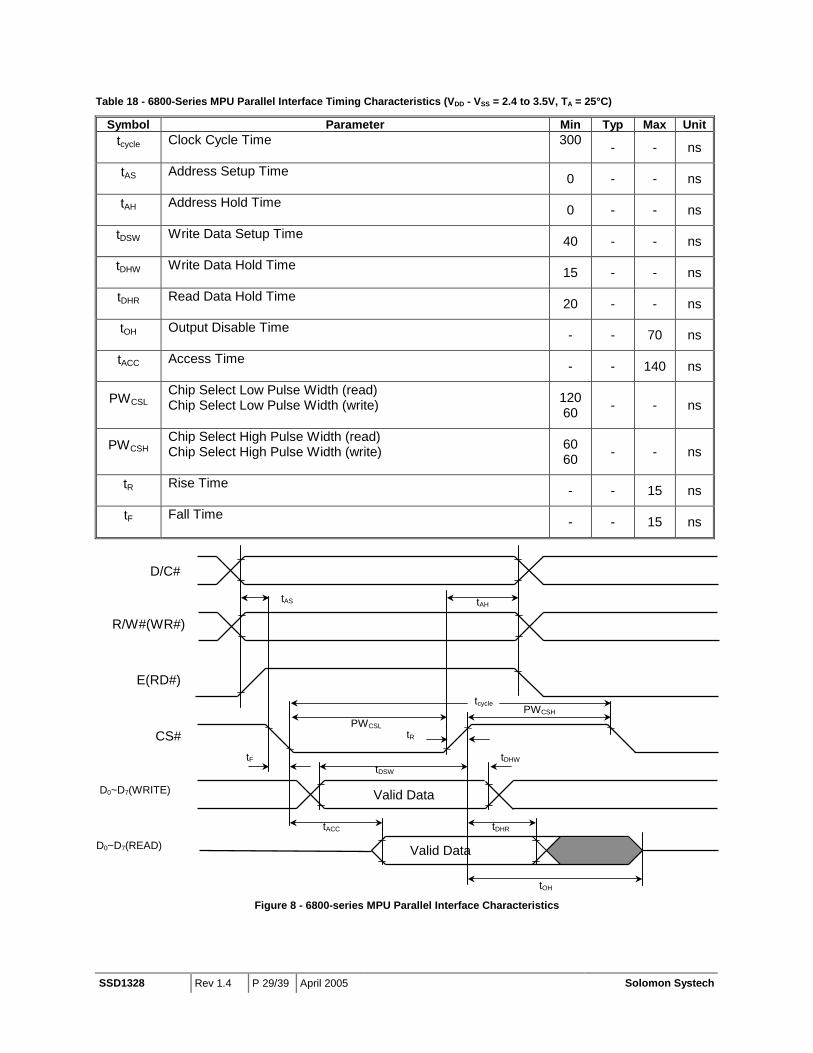
FUNCTIONAL BLOCK DESCRIPTIONS Command Decoder This module determines whether the input data is interpreted as data or command. Data is interpreted based upon the input of the D/C# pin. If D/C# pin is high, the input at D7-D0 is written to Graphic Display Data RAM (GDDRAM). If it is low, the input at D7-D0 is interpreted as a Command which will be decoded and be written to the corresponding command register. MPU Parallel 6800-series Interface The parallel interface consists of 8 bi-directional data pins (D7-D0), R/W#(WR#), D/C#, E (RD#), CS#. R/W#(WR#) input High indicates a read operation from the Graphic Display Data RAM (GDDRAM) or the status register. R/W# (WR#) input Low indicates a write operation to Display Data RAM or Internal Command Registers depending on the status of D/C# input. The E (RD#) input serves as data latch signal (clock) when high provided that CS# is low. Refer to Parallel Interface Timing Diagram of 6800-series microprocessors. In order to match the operating frequency of display RAM with that of the microprocessor, some pipeline processing is internally performed which requires the insertion of a dummy read before the first actual display data read. This is shown in Figure 3 below.
Figure 3 - Display Data Read Back Procedure - Insertion of Dummy Read
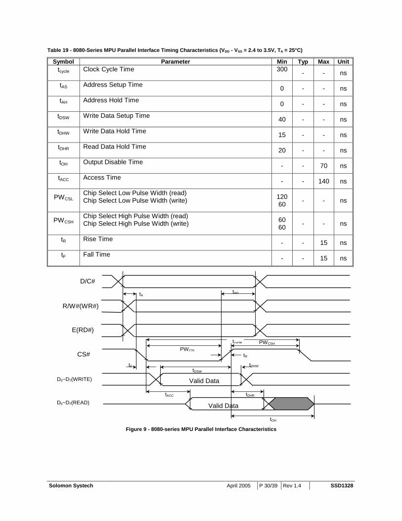
MPU Parallel 8080-series Interface The parallel interface consists of 8 bi-directional data pins (D7-D0), E (RD#), R/W#(WR#), D/C#, CS#. The E (RD#) input serves as data read latch signal (clock) when it is low, and provided that CS# is low. Display data or status register read is controlled by D/C#. R/W# (WR#) input serves as data write latch signal (clock) when it is high and provided that CS# is low. Display data or command register write is controlled by D/C#. Refer to Parallel Interface Timing Diagram of 8080-series microprocessor. Similar to 6800-series interface, a dummy read is also required before the first actual display data read.
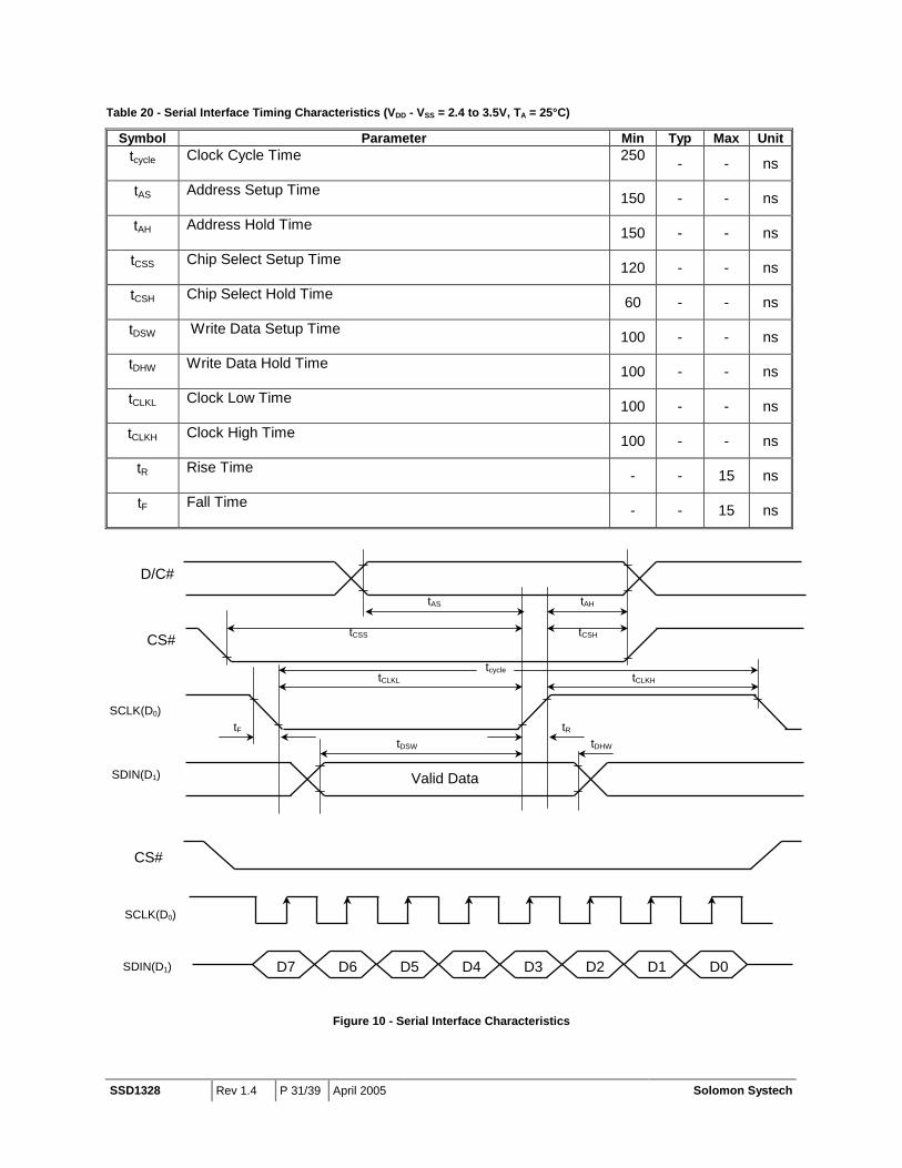
MPU Serial Interface The serial interface consists of serial clock SCLK, serial data SDIN, D/C#, CS#. SDIN is shifted into an 8-bit shift register on every rising edge of SCLK in the order of D7, D6, ... D0. D/C is sampled on every eighth clock and the data byte in the shift register is written to the Display Data RAM or command register in the same clock.
n+2 n+1
Write address Dummy read Data read1
R/W#(WR#)
DataN n
E(RD#)
Data read2 Data read3
SSD1328 Rev 1.4 P 15/39 April 2005 Solomon Systech
During data writing, an additional NOP command should be inserted before the CS# goes high (Refer to Figure 4.
Figure 4 - Display data write procedure in SPI mode
D7 D6 D5 D4 D3 D2 D1 D0
SCKL(D0)
SDIN(D1)
DB1 DB2 DBn NOP COMMAND
CS#
D/C
SDIN/SCLK
Reset Circuit When RES# input is low, the chip is initialized with the following status:
1. Display is OFF 2. 128x128 Display Mode 3. Normal segment and display data column address and row address mapping (SEG0 mapped to
address 00H and COM0 mapped to address 00H) 4. Shift register data clear in serial interface 5. Display start line is set at display RAM address 0 6. Column address counter is set at 0 7. Normal scan direction of the COM outputs 8. Contrast control register is set at 40H 9. Set quarter current range
Solomon Systech April 2005 P 16/39 Rev 1.4 SSD1328
Oscillator Circuit and Display Time Generator
Figure 5 - Oscillator Circuit
This module is an On-Chip low power RC oscillator circuitry (Figure 5). The oscillator generates the clock for the Display Timing Generator.
Current Control and Voltage Control This block is used to derive the incoming power sources into the different levels of internal use voltage and current. VCC and VDD are external power supplies. VREF is reference voltage, which is used to derive driving voltage for segments and commons. IREF is a reference current source for segment current drivers.
Segment Drivers/Common Drivers Segment drivers deliver 128 current sources to drive OLED panel. The driving current can be adjusted from 0 to 300uA with 128 steps. Common drivers generate voltage scanning pulse.
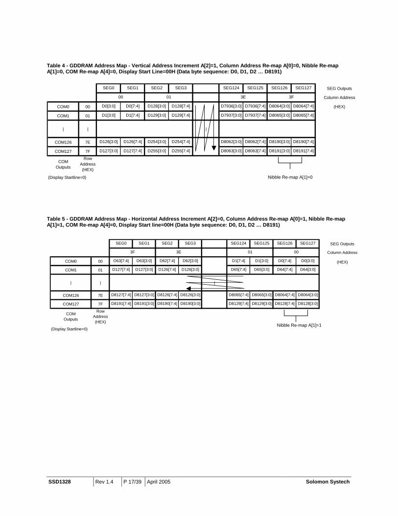
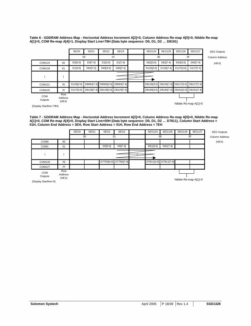
Graphic Display Data RAM (GDDRAM) The GDDRAM is a bit mapped static RAM holding the bit pattern to be displayed. The size of the RAM is 128x128x4 bits. See the description of the GDDRAM address map in Table 3 -Table 7 on page16 - 18. For mechanical flexibility, re-mapping on both Segment and Common outputs can be selected by software. For vertical scrolling of the display, an internal register storing display start line can be set to control the portion of the RAM data to be mapped to the display. Table 6 shows the example in which the display start line register is set to 78H. Graphic Display Data RAM (GDDRAM) Address Map
Table 3 - GDDRAM Address Map - Horizontal Address Increment A[2]=0, Column Address Re-map A[0]=0, Nibble Re-map A[1]=0, COM Re-map A[4]=0, Display Start Line=00H (Data byte sequence: D0, D1, D2 … D8191)
Nibble Re-map A[1]=0
Divider
Internal Oscillator
MUX
CL CLK DCLK
Internal Display Clock
SEG Outputs
Column Address
COM0 00 (HEX)
COM1 01
| | |
COM126 7E
COM127 7F
COMOutputs
RowAddress(HEX)
3E 3F00 01
D0[3:0] D0[7:4]
D64[3:0] D64[7:4]
D1[3:0] D1[7:4]
D65[3:0] D65[7:4]
D8064[3:0] D8064[7:4] D8065[3:0] D8065[7:4]
D8128[3:0] D8128[7:4] D8129[3:0] D8129[7:4]
D62[3:0] D62[7:4] D63[3:0] D63[7:4]
D126[3:0] D126[7:4] D127[3:0] D127[7:4]
D8126[3:0] D8126[7:4] D8127[3:0] D8127[7:4]
D8190[3:0] D8190[7:4] D8191[3:0] D8191[7:4]
SEG0 SEG1 SEG2 SEG127SEG3 SEG124 SEG125 SEG126
SSD1328 Rev 1.4 P 17/39 April 2005 Solomon Systech
Table 4 - GDDRAM Address Map - Vertical Address Increment A[2]=1, Column Address Re-map A[0]=0, Nibble Re-map A[1]=0, COM Re-map A[4]=0, Display Start Line=00H (Data byte sequence: D0, D1, D2 … D8191)
Table 5 - GDDRAM Address Map - Horizontal Address Increment A[2]=0, Column Address Re-map A[0]=1, Nibble Re-map A[1]=1, COM Re-map A[4]=0, Display Start line=00H (Data byte sequence: D0, D1, D2 … D8191)
Nibble Re-map A[1]=0
SEG Outputs
Column Address
COM0 00 (HEX)
COM1 01
| | |
COM126 7E
COM127 7F
COMOutputs
RowAddress(HEX)
(Display Startline=0)
D0[3:0] D0[7:4] D128[3:0] D128[7:4]
D1[3:0] D1[7:4] D129[3:0] D129[7:4]
D126[3:0] D126[7:4] D254[3:0] D254[7:4]
D127[3:0] D127[7:4] D255[3:0] D255[7:4]
D7936[3:0] D7936[7:4] D8064[3:0] D8064[7:4]
D7937[3:0] D7937[7:4] D8065[3:0] D8065[7:4]
D8062[3:0] D8062[7:4] D8190[3:0] D8190[7:4]
D8063[3:0] D8063[7:4] D8191[3:0] D8191[7:4]
00 01 3E 3F
SEG124 SEG125 SEG126 SEG127SEG0 SEG1 SEG2 SEG3
SEG Outputs
Column Address
COM0 00 (HEX)
COM1 01
| | |
COM126 7E
COM127 7F
COMOutputs
RowAddress(HEX)
(Display Startline=0)
3F 3E 01 00
SEG124 SEG125 SEG126 SEG127SEG0 SEG1 SEG2 SEG3
D8129[7:4] D8129[3:0] D8128[7:4] D8128[3:0]D8191[7:4] D8191[3:0] D8190[7:4] D8190[3:0]
D8065[7:4] D8065[3:0] D8064[7:4] D8064[3:0]D8127[7:4] D8127[3:0] D8126[7:4] D8126[3:0]
D65[7:4] D65[3:0] D64[7:4] D64[3:0]D127[7:4] D127[3:0] D126[7:4] D126[3:0]
D1[7:4] D1[3:0] D0[7:4] D0[3:0]D63[7:4] D63[3:0] D62[7:4] D62[3:0]
Nibble Re-map A[1]=1
Solomon Systech April 2005 P 18/39 Rev 1.4 SSD1328
Table 6 - GDDRAM Address Map - Horizontal Address Increment A[2]=0, Column Address Re-map A[0]=0, Nibble Re-map A[1]=0, COM Re-map A[4]=1, Display Start Line=78H (Data byte sequence: D0, D1, D2 … D8191)
Table 7 - GDDRAM Address Map - Horizontal Address Increment A[2]=0, Column Address Re-map A[0]=0, Nibble Re-map A[1]=0, COM Re-map A[4]=0, Display Start Line=00H (Data byte sequence: D0, D1, D2 … D7811), Column Start Address = 01H, Column End Address = 3EH, Row Start Address = 01H, Row End Address = 7EH
SEG Outputs
Column Address
COM0 00 (HEX)
COM1 01
| | |
COM126 7E
COM127 7F
COMOutputs
RowAddress(HEX)
(Display Startline=0)
SEG124SEG0 SEG125 SEG126 SEG127
00 01 3E 3F
SEG1 SEG2 SEG3
D0[3:0] D0[7:4] D61[3:0] D61[7:4]
D7750[3:0] D7750[7:4] D7811[3:0] D7811[7:4]
SEG Outputs
Column Address
COM119 00 (HEX)
COM118 01
| | |
COM121 7E
COM120 7F
COMOutputs
RowAddress(HEX)
(Display Startline=78H)
D63[3:0] D63[7:4]
00 01
D62[3:0] D62[7:4]D0[3:0] D0[7:4] D1[3:0] D1[7:4]
D1[3:0] D64[7:4] D65[3:0] D65[7:4]
3E 3F
D126[3:0] D126[7:4] D127[3:0] D127[7:4]
D126[3:0] D8064[7:4] D8065[3:0] D8065[7:4] D8127[3:0] D8127[7:4]
D127[3:0] D8128[7:4] D8129[3:0] D8129[7:4]
D8126[3:0] D8126[7:4]
D8190[3:0] D8190[7:4] D8191[3:0] D8191[7:4]
SEG0 SEG1 SEG2 SEG3 SEG124 SEG125 SEG126 SEG127
Nibble Re-map A[1]=0
Nibble Re-map A[1]=0
SSD1328 Rev 1.4 P 19/39 April 2005 Solomon Systech
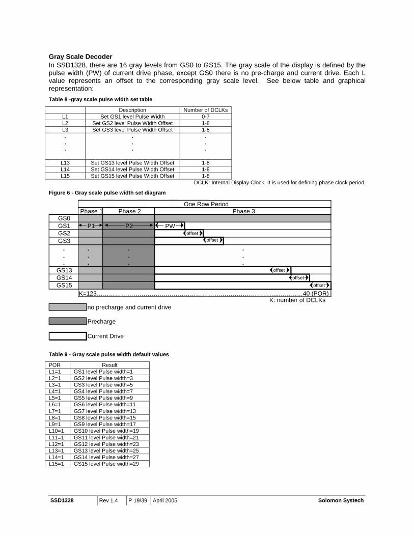
Gray Scale Decoder In SSD1328, there are 16 gray levels from GS0 to GS15. The gray scale of the display is defined by the pulse width (PW) of current drive phase, except GS0 there is no pre-charge and current drive. Each L value represents an offset to the corresponding gray scale level. See below table and graphical representation: Table 8 -gray scale pulse width set table
Description Number of DCLKs L1 Set GS1 level Pulse Width 0-7 L2 Set GS2 level Pulse Width Offset 1-8 L3 Set GS3 level Pulse Width Offset 1-8 . . .
.
.
.
.
.
.
L13 Set GS13 level Pulse Width Offset 1-8 L14 Set GS14 level Pulse Width Offset 1-8 L15 Set GS15 level Pulse Width Offset 1-8
DCLK: Internal Display Clock. It is used for defining phase clock period.
Figure 6 - Gray scale pulse width set diagram
Table 9 - Gray scale pulse width default values
POR Result L1=1 GS1 level Pulse width=1 L2=1 GS2 level Pulse width=3 L3=1 GS3 level Pulse width=5 L4=1 GS4 level Pulse width=7 L5=1 GS5 level Pulse width=9 L6=1 GS6 level Pulse width=11 L7=1 GS7 level Pulse width=13 L8=1 GS8 level Pulse width=15 L9=1 GS9 level Pulse width=17 L10=1 GS10 level Pulse width=19 L11=1 GS11 level Pulse width=21 L12=1 GS12 level Pulse width=23 L13=1 GS13 level Pulse width=25 L14=1 GS14 level Pulse width=27 L15=1 GS15 level Pulse width=29
GS0 GS1 P1 P2 GS2 GS3
. . .
. . .
. . . GS13 GS14 GS15
K: number of DCLKs no precharge and current drive
Precharge
Current Drive
.
.
K=123………………………….…………………………………………………..…………40 (POR)
One Row PeriodPhase 3
.
Phase 1 Phase 2
offset
offset offset
offset
PW
offset
Solomon Systech April 2005 P 20/39 Rev 1.4 SSD1328
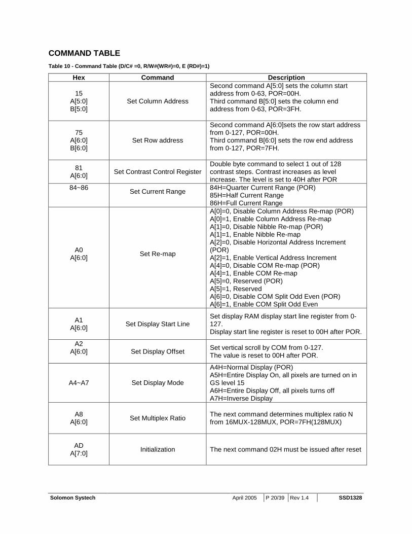
COMMAND TABLE Table 10 - Command Table (D/C# =0, R/W#(WR#)=0, E (RD#)=1)
Hex Command Description
15 A[5:0] B[5:0]
Set Column Address
Second command A[5:0] sets the column start address from 0-63, POR=00H. Third command B[5:0] sets the column end address from 0-63, POR=3FH.
75 A[6:0] B[6:0]
Set Row address
Second command A[6:0]sets the row start address from 0-127, POR=00H. Third command B[6:0] sets the row end address from 0-127, POR=7FH.
81 A[6:0] Set Contrast Control Register
Double byte command to select 1 out of 128 contrast steps. Contrast increases as level increase. The level is set to 40H after POR
84~86
Set Current Range
84H=Quarter Current Range (POR) 85H=Half Current Range 86H=Full Current Range
A0
A[6:0]
Set Re-map
A[0]=0, Disable Column Address Re-map (POR) A[0]=1, Enable Column Address Re-map A[1]=0, Disable Nibble Re-map (POR) A[1]=1, Enable Nibble Re-map A[2]=0, Disable Horizontal Address Increment (POR) A[2]=1, Enable Vertical Address Increment A[4]=0, Disable COM Re-map (POR) A[4]=1, Enable COM Re-map A[5]=0, Reserved (POR) A[5]=1, Reserved A[6]=0, Disable COM Split Odd Even (POR) A[6]=1, Enable COM Split Odd Even
A1
A[6:0]
Set Display Start Line Set display RAM display start line register from 0-127. Display start line register is reset to 00H after POR.
A2 A[6:0]
Set Display Offset Set vertical scroll by COM from 0-127.
The value is reset to 00H after POR.
A4~A7
Set Display Mode
A4H=Normal Display (POR) A5H=Entire Display On, all pixels are turned on in GS level 15 A6H=Entire Display Off, all pixels turns off A7H=Inverse Display
A8
A[6:0]
Set Multiplex Ratio The next command determines multiplex ratio N from 16MUX-128MUX, POR=7FH(128MUX)
AD
A[7:0]
Initialization The next command 02H must be issued after reset
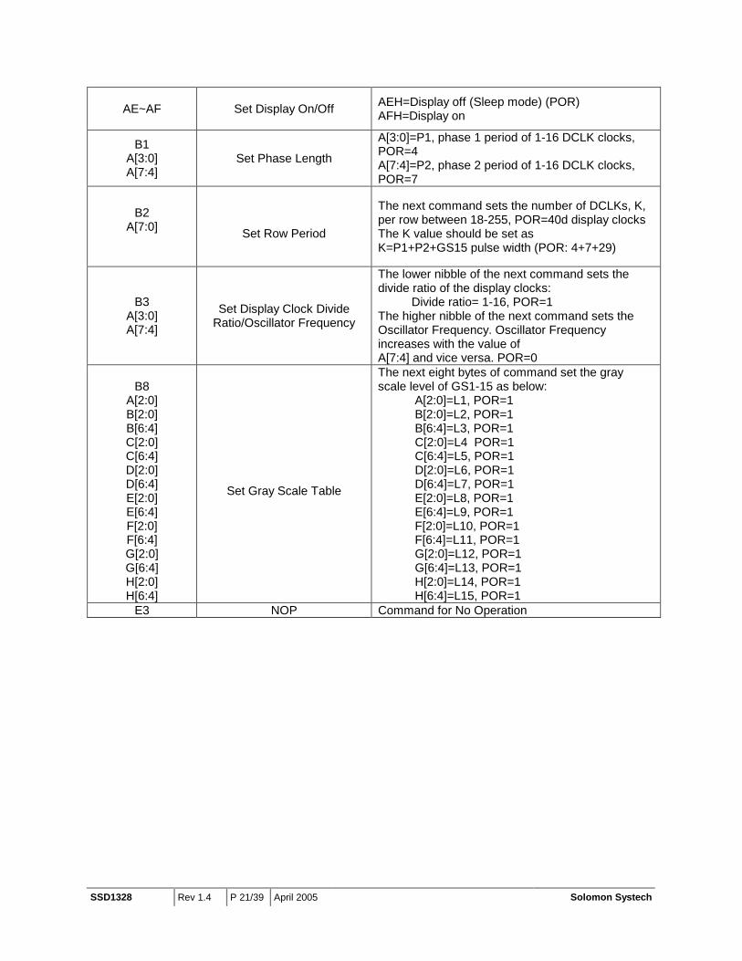
SSD1328 Rev 1.4 P 21/39 April 2005 Solomon Systech
AE~AF
Set Display On/Off
AEH=Display off (Sleep mode) (POR) AFH=Display on
B1 A[3:0] A[7:4]
Set Phase Length
A[3:0]=P1, phase 1 period of 1-16 DCLK clocks, POR=4 A[7:4]=P2, phase 2 period of 1-16 DCLK clocks, POR=7
B2
A[7:0]
Set Row Period
The next command sets the number of DCLKs, K, per row between 18-255, POR=40d display clocks The K value should be set as K=P1+P2+GS15 pulse width (POR: 4+7+29)
B3 A[3:0] A[7:4]
Set Display Clock Divide Ratio/Oscillator Frequency
The lower nibble of the next command sets the divide ratio of the display clocks: Divide ratio= 1-16, POR=1 The higher nibble of the next command sets the Oscillator Frequency. Oscillator Frequency increases with the value of A[7:4] and vice versa. POR=0
B8
A[2:0] B[2:0] B[6:4] C[2:0] C[6:4] D[2:0] D[6:4] E[2:0] E[6:4] F[2:0] F[6:4] G[2:0] G[6:4] H[2:0] H[6:4]
Set Gray Scale Table
The next eight bytes of command set the gray scale level of GS1-15 as below: A[2:0]=L1, POR=1 B[2:0]=L2, POR=1 B[6:4]=L3, POR=1 C[2:0]=L4 POR=1 C[6:4]=L5, POR=1 D[2:0]=L6, POR=1 D[6:4]=L7, POR=1 E[2:0]=L8, POR=1 E[6:4]=L9, POR=1 F[2:0]=L10, POR=1 F[6:4]=L11, POR=1 G[2:0]=L12, POR=1 G[6:4]=L13, POR=1 H[2:0]=L14, POR=1 H[6:4]=L15, POR=1
E3 NOP Command for No Operation
Solomon Systech April 2005 P 22/39 Rev 1.4 SSD1328
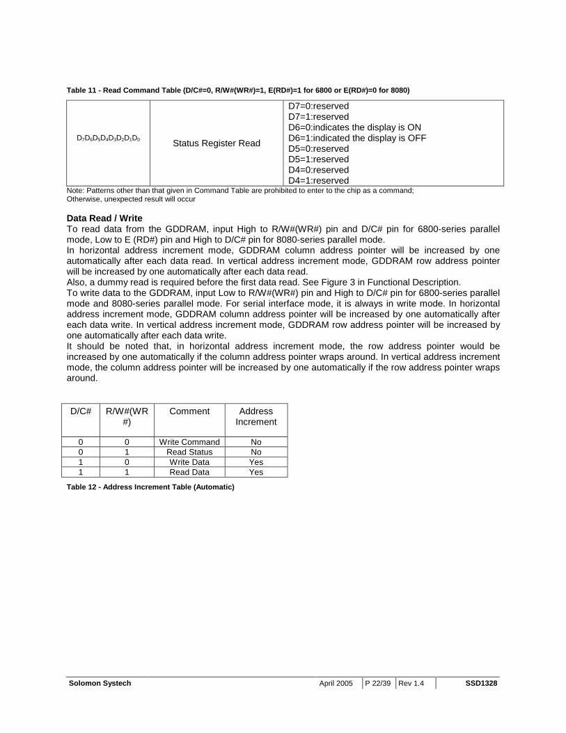
Table 11 - Read Command Table (D/C#=0, R/W#(WR#)=1, E(RD#)=1 for 6800 or E(RD#)=0 for 8080)
D7D6D5D4D3D2D1D0 Status Register Read
D7=0:reserved D7=1:reserved D6=0:indicates the display is ON D6=1:indicated the display is OFF D5=0:reserved D5=1:reserved D4=0:reserved D4=1:reserved
Note: Patterns other than that given in Command Table are prohibited to enter to the chip as a command; Otherwise, unexpected result will occur Data Read / Write To read data from the GDDRAM, input High to R/W#(WR#) pin and D/C# pin for 6800-series parallel mode, Low to E (RD#) pin and High to D/C# pin for 8080-series parallel mode. In horizontal address increment mode, GDDRAM column address pointer will be increased by one automatically after each data read. In vertical address increment mode, GDDRAM row address pointer will be increased by one automatically after each data read. Also, a dummy read is required before the first data read. See Figure 3 in Functional Description. To write data to the GDDRAM, input Low to R/W#(WR#) pin and High to D/C# pin for 6800-series parallel mode and 8080-series parallel mode. For serial interface mode, it is always in write mode. In horizontal address increment mode, GDDRAM column address pointer will be increased by one automatically after each data write. In vertical address increment mode, GDDRAM row address pointer will be increased by one automatically after each data write. It should be noted that, in horizontal address increment mode, the row address pointer would be increased by one automatically if the column address pointer wraps around. In vertical address increment mode, the column address pointer will be increased by one automatically if the row address pointer wraps around.
D/C#
R/W#(WR
#)
Comment
Address Increment
0 0 Write Command No 0 1 Read Status No 1 0 Write Data Yes 1 1 Read Data Yes
Table 12 - Address Increment Table (Automatic)
SSD1328 Rev 1.4 P 23/39 April 2005 Solomon Systech
COMMAND DESCRIPTIONS
Set Column Address This command specifies column start address and end address of the display data RAM. This command also sets the column address pointer to column start address.
Set Row Address This command specifies row start address and end address of the display data RAM. This command also sets the row address pointer to row start address.
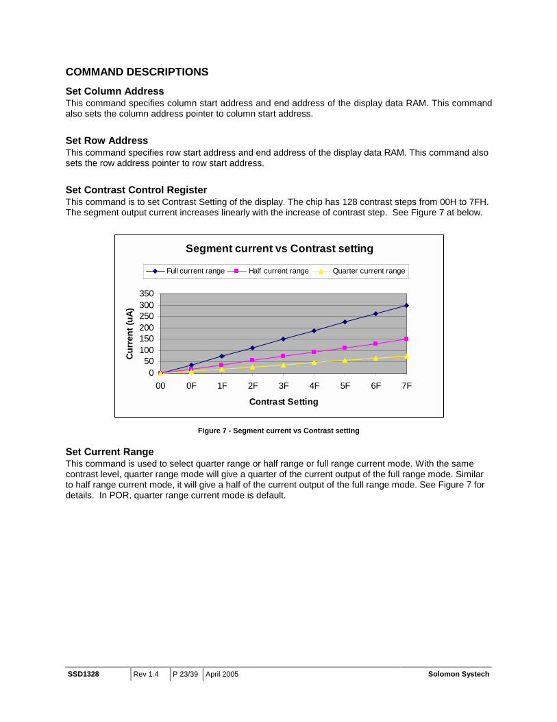
Set Contrast Control Register This command is to set Contrast Setting of the display. The chip has 128 contrast steps from 00H to 7FH. The segment output current increases linearly with the increase of contrast step. See Figure 7 at below.
Figure 7 - Segment current vs Contrast setting
Set Current Range This command is used to select quarter range or half range or full range current mode. With the same contrast level, quarter range mode will give a quarter of the current output of the full range mode. Similar to half range current mode, it will give a half of the current output of the full range mode. See Figure 7 for details. In POR, quarter range current mode is default.
Segment current vs Contrast setting
050
100150200250300350
00 0F 1F 2F 3F 4F 5F 6F 7F
Contrast Setting
Cur
rent
(uA)
Full current range Half current range Quarter current range
Solomon Systech April 2005 P 24/39 Rev 1.4 SSD1328
Set Re-map This command changes the mapping between the display data column address and segment driver, row address and common driver. It allows flexibility in layout during OLED module assembly. See the Re-map setting below: Column Address Re-map If column address re-map is set, Col 0-63 map to SEG127-0, regardless of start column and end column commands. Nibble Re-map If nibble re-map is set, the two nibbles of the data bus for RAM access are re-mapped, such that (D7, D6, D5, D4, D3, D2, D1, D0) acts like (D3, D2, D1, D0, D7, D6, D5, D4) This feature working with Column Address Re-map would produce an effect of flipping outputs SEG0-127 to SEG127-SEG0. Address Increment Mode If horizontal increment mode is set, the column address pointer advances after each RAM access. If vertical increment mode is set, the row address pointer advances after each RAM access. COM Re-map This 3-bit command is used to set the mapping for COM signals. If COM re-map is set, ROW 0-127 maps to COM127-0, regardless of start and end row commands. If COM split odd even is set, ROW0,2,4,…,62 map to COM0-63, ROW1,3,5,…,63 map to COM64-127. See Table 13 below:
A[4:6] COM 0-127 000 ROW 0-127 100 ROW 127-0
A[4:6] COM0,1,2,…,63 COM64,65,66,…,127 000 ROW0,1,2,…,63 ROW64,65,66,…,127001 ROW0,2,4,…,126 ROW1,3,5,…,127
Table 13 - COM Re-map setting
Set Display Start Line This command is to set Display Start Line register to determine starting address of display RAM to be displayed by selecting a value from 0 to 127.
Set Display Offset This is a double byte command. The next command specifies the mapping of display start line (it is assumed that COM0 is the display start line, display start line register equals to 0) to one of COM0-127. For example, to move the COM16 towards the COM0 direction for 16 lines, the 7-bit data in the second command should be given by 0010000. To move in the opposite direction by 16 lines, the 6-bit data should be given by (128-16) and so the second command should be 1110000.
SSD1328 Rev 1.4 P 25/39 April 2005 Solomon Systech
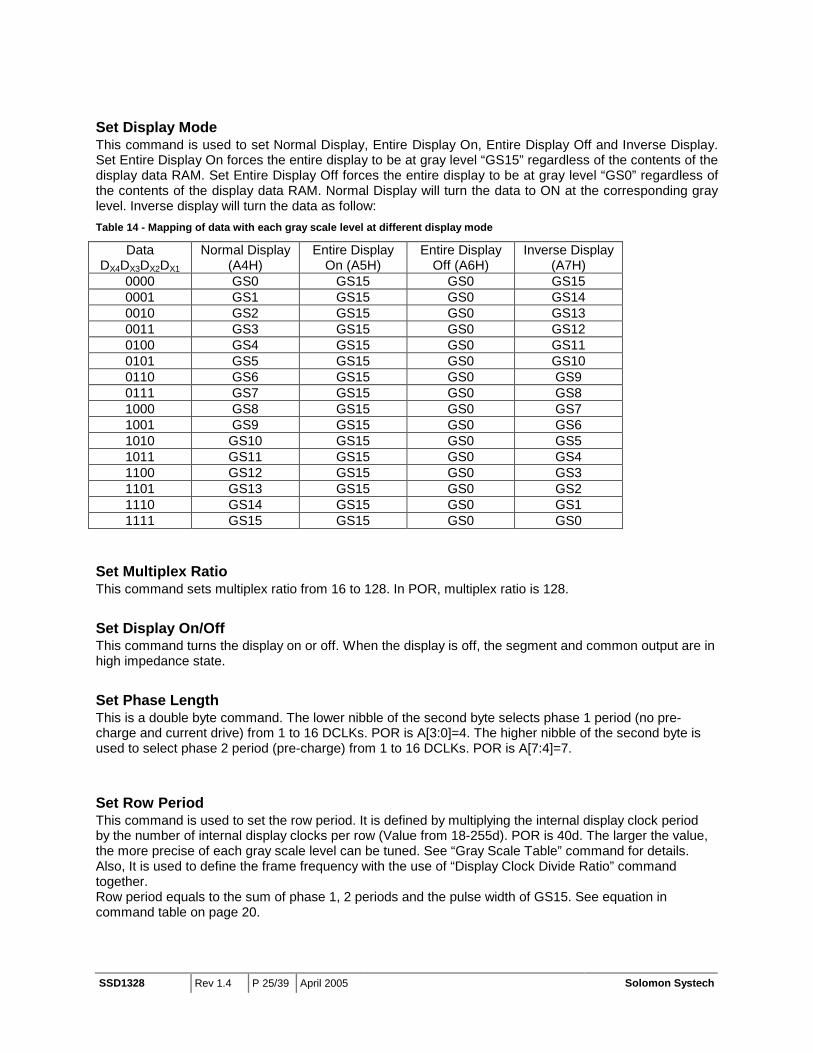
Set Display Mode This command is used to set Normal Display, Entire Display On, Entire Display Off and Inverse Display. Set Entire Display On forces the entire display to be at gray level “GS15” regardless of the contents of the display data RAM. Set Entire Display Off forces the entire display to be at gray level “GS0” regardless of the contents of the display data RAM. Normal Display will turn the data to ON at the corresponding gray level. Inverse display will turn the data as follow: Table 14 - Mapping of data with each gray scale level at different display mode
Data DX4DX3DX2DX1
Normal Display (A4H)
Entire Display On (A5H)
Entire Display Off (A6H)
Inverse Display (A7H)
0000 GS0 GS15 GS0 GS15 0001 GS1 GS15 GS0 GS14 0010 GS2 GS15 GS0 GS13 0011 GS3 GS15 GS0 GS12 0100 GS4 GS15 GS0 GS11 0101 GS5 GS15 GS0 GS10 0110 GS6 GS15 GS0 GS9 0111 GS7 GS15 GS0 GS8 1000 GS8 GS15 GS0 GS7 1001 GS9 GS15 GS0 GS6 1010 GS10 GS15 GS0 GS5 1011 GS11 GS15 GS0 GS4 1100 GS12 GS15 GS0 GS3 1101 GS13 GS15 GS0 GS2 1110 GS14 GS15 GS0 GS1 1111 GS15 GS15 GS0 GS0
Set Multiplex Ratio This command sets multiplex ratio from 16 to 128. In POR, multiplex ratio is 128.
Set Display On/Off This command turns the display on or off. When the display is off, the segment and common output are in high impedance state.
Set Phase Length This is a double byte command. The lower nibble of the second byte selects phase 1 period (no pre-charge and current drive) from 1 to 16 DCLKs. POR is A[3:0]=4. The higher nibble of the second byte is used to select phase 2 period (pre-charge) from 1 to 16 DCLKs. POR is A[7:4]=7.
Set Row Period This command is used to set the row period. It is defined by multiplying the internal display clock period by the number of internal display clocks per row (Value from 18-255d). POR is 40d. The larger the value, the more precise of each gray scale level can be tuned. See “Gray Scale Table” command for details. Also, It is used to define the frame frequency with the use of “Display Clock Divide Ratio” command together. Row period equals to the sum of phase 1, 2 periods and the pulse width of GS15. See equation in command table on page 20.
Solomon Systech April 2005 P 26/39 Rev 1.4 SSD1328
Set Display Clock Divide Ratio This command is used to set the frequency of the internal display clocks, DCLKs. It is defined by dividing the oscillator frequency by the divide ratio (Value from 1 to 16). POR is 1. Frame frequency is determined by divide ratio, number of display clocks per row, MUX ratio and oscillator frequency. See equation on page 20.
Set Oscillator Frequency This is a double byte command. The lower nibble of the second byte is used to select the oscillator frequency. Default value is shown in Table 17 on page 28.
Set Gray Scale Table This command is used to set the gray scale table for the display. Except GS0, which has no pre-charge and current drive, each GS level is programmed by a set of offset values. As shown in Table 8, GS1 is defined with pulse width equals to the first offset value, L1, select from 0-7 internal display clocks. GS2 is defined with pulse width equals to GS1 plus the next offset value, L2, select from1-8 internal display clocks. Similarly, the next GS level is defined with pulse width equals to its lower one GS level plus the next offset value, select from 1-8 internal display clocks. In normal operation, GS15 should take the full current drive period as its pulse width. Therefore, the row period should be set as the sum of phase 1 period, phase 2 period, and the pulse width of GS15 with the use of “Row period” command.
NOP No Operation Command.
Status register Read This command is issued by setting D/C# low during a data read (refer to Figure 8 and Figure 9 parallel interface waveform). It allows the MCU to monitor the internal status of the chip.
SSD1328 Rev 1.4 P 27/39 April 2005 Solomon Systech
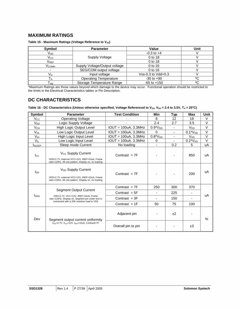
MAXIMUM RATINGS Table 15 - Maximum Ratings (Voltage Reference to VSS)
Symbol Parameter Value Unit VDD -0.3 to +4 V VCC 0 to 18 V VREF
Supply Voltage 0 to 18 V
VCOMH Supply Voltage/Output voltage 0 to 16 V - SEG/COM output voltage 0 to 16 V
Vin Input voltage Vss-0.3 to Vdd+0.3 V TA Operating Temperature -30 to +90 ºC Tstg Storage Temperature Range -65 to +150 ºC
*Maximum Ratings are those values beyond which damage to the device may occur. Functional operation should be restricted to the limits in the Electrical Characteristics tables or Pin Description.
DC CHARACTERISTICS Table 16 - DC Characteristics (Unless otherwise specified, Voltage Referenced to VSS, VDD = 2.4 to 3.5V, TA = 25°°°°C)
Symbol Parameter Test Condition Min Typ Max Unit VCC Operating Voltage - 8 12 18 V VDD Logic Supply Voltage - 2.4 2.7 3.5 V VOH High Logic Output Level IOUT = 100uA, 3.3MHz 0.9*VDD - VDD V VOL Low Logic Output Level IOUT = 100uA, 3.3MHz 0 - 0.1*VDD V VIH High Logic Input Level IOUT = 100uA, 3.3MHz 0.8*VDD - VDD V VIL Low Logic Input Level IOUT = 100uA, 3.3MHz 0 - 0.2*VDD V
ISLEEP Sleep mode Current No loading - 0.2 5 uA
ICC
VCC Supply Current
VDD=2.7V, external VCC=12V, IREF=10uA, Frame rate=110Hz, All one pattern, Display on, no loading
Contrast = 7F - - 850 uA
IDD
VDD Supply Current
VDD=2.7V, external VCC=12V, IREF=10uA, Frame rate=110Hz, All one pattern, Display on, no loading
Contrast = 7F - - 200 uA
Contrast = 7F 250 300 370 Contrast = 5F - 225 - Contrast = 3F - 150 -
ISEG Segment Output Current
VDD=2.7V, VCC=12V, IREF=10uA, Frame
rate=110Hz, Display on, Segment pin under test is connected with a 20K resistive load to VSS
Contrast = 1F 50 75 100
uA
Adjacent pin - ±2 - Dev
Segment output current uniformity
VDD=2.7V, VCC=12V, IREF=10uA, Contrast=7F Overall pin to pin - - ±3
%
Solomon Systech April 2005 P 28/39 Rev 1.4 SSD1328
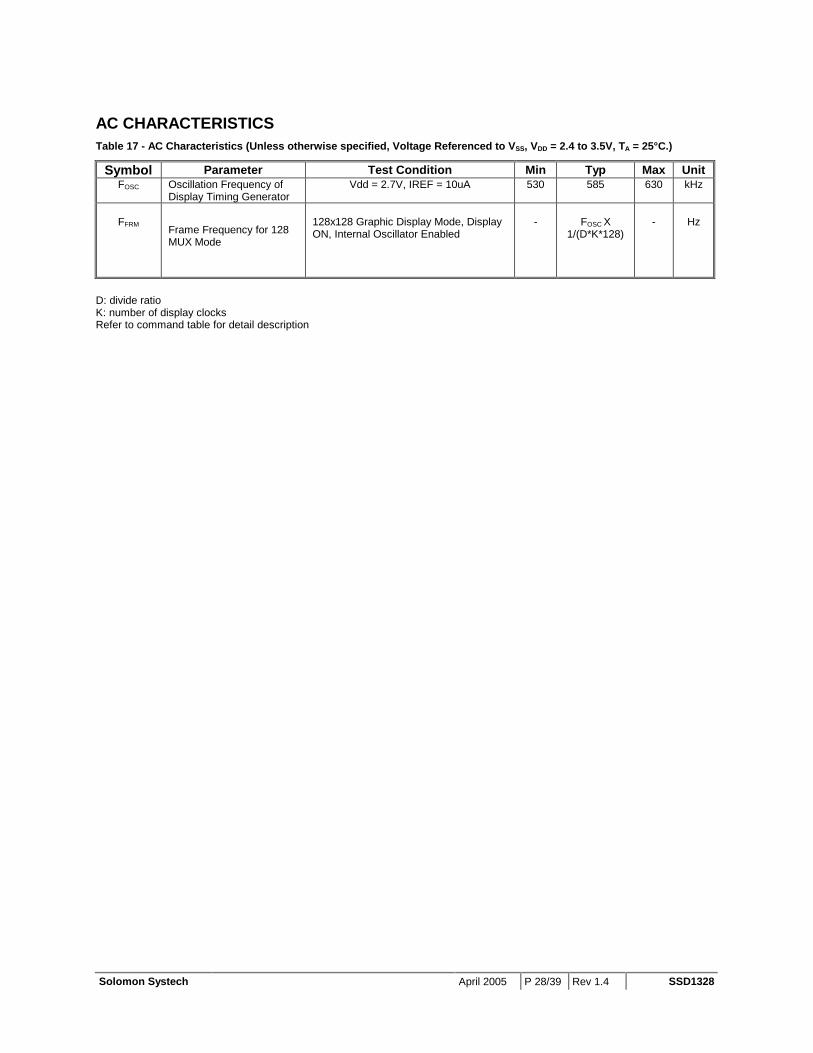
AC CHARACTERISTICS Table 17 - AC Characteristics (Unless otherwise specified, Voltage Referenced to VSS, VDD = 2.4 to 3.5V, TA = 25°C.)
Symbol Parameter Test Condition Min Typ Max Unit FOSC Oscillation Frequency of
Display Timing Generator Vdd = 2.7V, IREF = 10uA
530 585 630 kHz
FFRM
Frame Frequency for 128 MUX Mode
128x128 Graphic Display Mode, Display ON, Internal Oscillator Enabled
-
FOSC X 1/(D*K*128)
-
Hz
D: divide ratio K: number of display clocks Refer to command table for detail description
SSD1328 Rev 1.4 P 29/39 April 2005 Solomon Systech
Table 18 - 6800-Series MPU Parallel Interface Timing Characteristics (VDD - VSS = 2.4 to 3.5V, TA = 25°C)
Symbol Parameter Min Typ Max Unit tcycle
Clock Cycle Time
300
- - ns
tAS
Address Setup Time 0 - - ns
tAH
Address Hold Time 0 - - ns
tDSW
Write Data Setup Time 40 - - ns
tDHW
Write Data Hold Time 15 - - ns
tDHR
Read Data Hold Time 20 - - ns
tOH
Output Disable Time - - 70 ns
tACC
Access Time - - 140 ns
PWCSL
Chip Select Low Pulse Width (read) Chip Select Low Pulse Width (write)
120 60 - - ns
PWCSH
Chip Select High Pulse Width (read) Chip Select High Pulse Width (write)
60 60 - - ns
tR
Rise Time - - 15 ns
tF
Fall Time - - 15 ns
Figure 8 - 6800-series MPU Parallel Interface Characteristics
D0~D7(WRITE)
D0~D7(READ)
E(RD#)
CS#
R/W#(WR#)
PWCSL tR
tF tDHW
tOH
tACC tDHR
Valid Data
tDSW
Valid Data
tcycle PWCSH
tAH tAS
D/C#
Solomon Systech April 2005 P 30/39 Rev 1.4 SSD1328
Table 19 - 8080-Series MPU Parallel Interface Timing Characteristics (VDD - VSS = 2.4 to 3.5V, TA = 25°C)
Symbol Parameter Min Typ Max Unit tcycle
Clock Cycle Time
300
- - ns
tAS
Address Setup Time 0 - - ns
tAH
Address Hold Time 0 - - ns
tDSW
Write Data Setup Time 40 - - ns
tDHW
Write Data Hold Time 15 - - ns
tDHR
Read Data Hold Time 20 - - ns
tOH
Output Disable Time - - 70 ns
tACC
Access Time - - 140 ns
PWCSL
Chip Select Low Pulse Width (read) Chip Select Low Pulse Width (write)
120 60 - - ns
PWCSH
Chip Select High Pulse Width (read) Chip Select High Pulse Width (write)
60 60 - - ns
tR
Rise Time - - 15 ns
tF
Fall Time - - 15 ns
Figure 9 - 8080-series MPU Parallel Interface Characteristics
PWCSH PWCSL
tF tDSW
tDHW
tOH
tACC
Valid Data
tDHR
Valid Data
tcycle
tAH tA
D/C#
E(RD#)
CS#
D0~D7(WRITE)
D0~D7(READ)
R/W#(WR#)
tR
SSD1328 Rev 1.4 P 31/39 April 2005 Solomon Systech
Table 20 - Serial Interface Timing Characteristics (VDD - VSS = 2.4 to 3.5V, TA = 25°C)
Symbol Parameter Min Typ Max Unit tcycle
Clock Cycle Time
250
- - ns
tAS
Address Setup Time 150 - - ns
tAH
Address Hold Time 150 - - ns
tCSS
Chip Select Setup Time 120 - - ns
tCSH
Chip Select Hold Time 60 - - ns
tDSW
Write Data Setup Time 100 - - ns
tDHW
Write Data Hold Time 100 - - ns
tCLKL
Clock Low Time 100 - - ns
tCLKH
Clock High Time 100 - - ns
tR
Rise Time - - 15 ns
tF
Fall Time - - 15 ns
Figure 10 - Serial Interface Characteristics
tAH tAS
D/C#
Valid Data
tDHW
tCLKL
tDSW
tCLKH tcycle
tCSS tCSH
tF tR
SDIN(D1)
CS#
SCLK(D0)
D7 SDIN(D1)
CS#
SCLK(D0)
D6 D5 D4 D3 D2 D1 D0
Solomon Systech
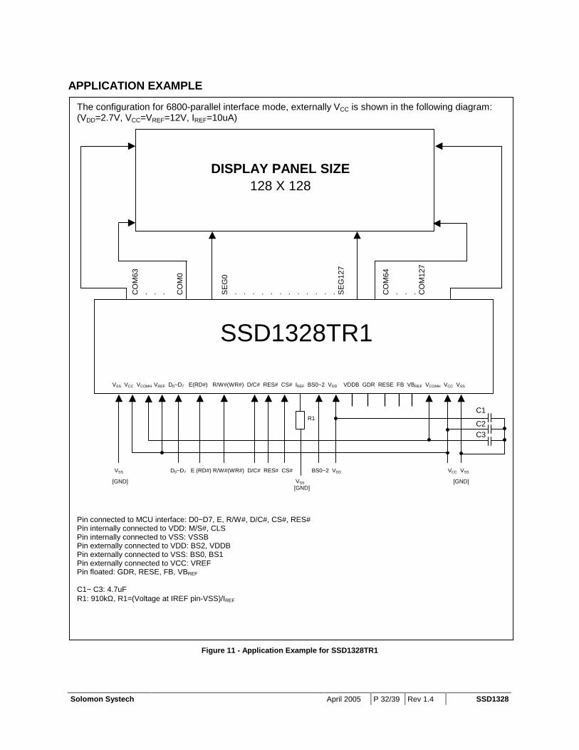
The configuration for 6800-parallel interface mode, externally VCC is shown in the following diagram: (VDD=2.7V, VCC=VREF=12V, IREF=10uA) Pin connected to MCU inPin internally connected tPin internally connected tPin externally connected Pin externally connected Pin externally connected Pin floated: GDR, RESE, C1~ C3: 4.7uF R1: 910kΩ, R1=(Voltage
APPLICATION EXAMPLE
DISPLAY PANEL SIZE 128 X 128
CO
M63
. .
7 7
VSS VCC VCOMH VR
terface: D0~D7,o VDD: M/S#, Co VSS: VSSB to VDD: BS2, Vto VSS: BS0, BSto VCC: VREF FB, VBREF
at IREF pin-VSS
Figu
. CO
M0
SE
G0
. . . . . . . . . . . . SE
G12
CO
M64
. . . CO
M12
EF D0~D7 E(RD#) R
SSD1328TR1
/W#(WR#) D/C# RES# CS# IREF BS0~2 VDD VDDB GDR RESE FB VBREF VCOMH VCC VSS
R1
C1
C2C3
[GND] VSS [GND]
VSS D0~D7 E (RD#) R/W#(WR#) D/C# RES# CS# BS0~2 VDD VCC VSS
April 2005 P 32/39 Rev 1.4 SSD1328
E, R/W#, D/C#, CS#, RES# LS
DDB 1
)/IREF
re 11 - Application Example for SSD1328TR1
[GND]
SSD1328 Rev 1.4 P 33/39 April 2005 Solomon Systech
SOLOMON
SOLOMON SSD1328T
SSD1328T
SSD1328TR1 TAB PACKAGE DIMENSION
Solomon Systech April 2005 P 34/39 Rev 1.4 SSD1328
SSD1328 Rev 1.4 P 35/39 April 2005 Solomon Systech
SSD1328TR1 PIN ASSIGNMENT
Figure 12 - SSD1328TR1 TAB pin assignment (Copper view, Mirror TAB design)
328327326325324. . . 265264263262. . 245244243242. . . . 119118117116. . 99 98 97 96 . . . 37 36 35 34 33
DUMMY DUMMY COM63 COM62 COM61 . . . COM2 COM1 COM0 DUMMY . . DUMMY SEG0 SEG1 SEG2 . . . . SEG125 SEG126 SEG127 DUMMY . . DUMMY COM64 COM65 COM66 . . . COM125 COM126 COM127 DUMMY DUMMY
1 2 3 4 5 6 7 8 9 10 11 12 13 14 15 16 17 18 19 20 21 22 23 24 25 26 27 28 29 30 31 32
DUMMY VSS VCC VCOMH VREF D7 D6 D5 D4 D3 D2 D1 D0 E(RD#) R/W#(WR#) D/C# RES# CS# IREF BS2 BS1 BS0 VDD VDDB VBREF RESE FB GDR VCOMH VCC VSS VSSB
Solomon Systech April 2005 P 36/39 Rev 1.4 SSD1328
Note: Dummy pin should be in no connection and do not group them together.
Table 21 - SSD1328TR1 pin assignment
PIN NO. PIN NAME PIN NO. PIN NAME PIN NO. PIN NAME PIN NO. PIN NAME PIN NO. PIN NAME PIN NO. PIN NAME
1 DUMMY 33 DUMMY 99 DUMMY 149 SEG95 213 SEG31 263 COM02 VSS 34 DUMMY 100 DUMMY 150 SEG94 214 SEG30 264 COM13 VCC 35 COM127 101 DUMMY 151 SEG93 215 SEG29 265 COM24 VCOMH 36 COM126 102 DUMMY 152 SEG92 216 SEG28 266 COM35 VREF 37 COM125 103 DUMMY 153 SEG91 217 SEG27 267 COM46 D7 38 COM124 104 DUMMY 154 SEG90 218 SEG26 268 COM57 D6 39 COM123 105 DUMMY 155 SEG89 219 SEG25 269 COM68 D5 40 COM122 106 DUMMY 156 SEG88 220 SEG24 270 COM79 D4 41 COM121 107 DUMMY 157 SEG87 221 SEG23 271 COM810 D3 42 COM120 108 DUMMY 158 SEG86 222 SEG22 272 COM911 D2 43 COM119 109 DUMMY 159 SEG85 223 SEG21 273 COM1012 D1 44 COM118 110 DUMMY 160 SEG84 224 SEG20 274 COM1113 D0 45 COM117 111 DUMMY 161 SEG83 225 SEG19 275 COM1214 E(RD#) 46 COM116 112 DUMMY 162 SEG82 226 SEG18 276 COM1315 R/W#(WR#) 47 COM115 113 DUMMY 163 SEG81 227 SEG17 277 COM1416 D/C# 48 COM114 114 DUMMY 164 SEG80 228 SEG16 278 COM1517 RES# 49 COM113 115 DUMMY 165 SEG79 229 SEG15 279 COM1618 CS# 50 COM112 116 DUMMY 166 SEG78 230 SEG14 280 COM1719 IREF 51 COM111 117 SEG127 167 SEG77 231 SEG13 281 COM1820 BS2 52 COM110 118 SEG126 168 SEG76 232 SEG12 282 COM1921 BS1 53 COM109 119 SEG125 169 SEG75 233 SEG11 283 COM2022 BS0 54 COM108 120 SEG124 170 SEG74 234 SEG10 284 COM2123 VDD 55 COM107 121 SEG123 171 SEG73 235 SEG9 285 COM2224 VDDB 56 COM106 122 SEG122 172 SEG72 236 SEG8 286 COM2325 VBREF 57 COM105 123 SEG121 173 SEG71 237 SEG7 287 COM2426 RESE 58 COM104 124 SEG120 174 SEG70 238 SEG6 288 COM2527 FB 59 COM103 125 SEG119 175 SEG69 239 SEG5 289 COM2628 GDR 60 COM102 126 SEG118 176 SEG68 240 SEG4 290 COM2729 VCOMH 61 COM101 127 SEG117 177 SEG67 241 SEG3 291 COM2830 VCC 62 COM100 128 SEG116 178 SEG66 242 SEG2 292 COM2931 VSS 63 COM99 129 SEG115 179 SEG65 243 SEG1 293 COM3032 VSSB 64 COM98 130 SEG114 180 SEG64 244 SEG0 294 COM31
65 COM97 131 SEG113 181 SEG63 245 DUMMY 295 COM3266 COM96 132 SEG112 182 SEG62 246 DUMMY 296 COM3367 COM95 133 SEG111 183 SEG61 247 DUMMY 297 COM3468 COM94 134 SEG110 184 SEG60 248 DUMMY 298 COM3569 COM93 135 SEG109 185 SEG59 249 DUMMY 299 COM3670 COM92 136 SEG108 186 SEG58 250 DUMMY 300 COM3771 COM91 137 SEG107 187 SEG57 251 DUMMY 301 COM3872 COM90 138 SEG106 188 SEG56 252 DUMMY 302 COM3973 COM89 139 SEG105 189 SEG55 253 DUMMY 303 COM4074 COM88 140 SEG104 190 SEG54 254 DUMMY 304 COM4175 COM87 141 SEG103 191 SEG53 255 DUMMY 305 COM4276 COM86 142 SEG102 192 SEG52 256 DUMMY 306 COM4377 COM85 143 SEG101 193 SEG51 257 DUMMY 307 COM4478 COM84 144 SEG100 194 SEG50 258 DUMMY 308 COM4579 COM83 145 SEG99 195 SEG49 259 DUMMY 309 COM4680 COM82 146 SEG98 196 SEG48 260 DUMMY 310 COM4781 COM81 147 SEG97 197 SEG47 261 DUMMY 311 COM4882 COM80 148 SEG96 198 SEG46 262 DUMMY 312 COM49
83 COM79 199 SEG45 313 COM5084 COM78 200 SEG44 314 COM5185 COM77 201 SEG43 315 COM5286 COM76 202 SEG42 316 COM5387 COM75 203 SEG41 317 COM5488 COM74 204 SEG40 318 COM5589 COM73 205 SEG39 319 COM5690 COM72 206 SEG38 320 COM5791 COM71 207 SEG37 321 COM5892 COM70 208 SEG36 322 COM5993 COM69 209 SEG35 323 COM6094 COM68 210 SEG34 324 COM6195 COM67 211 SEG33 325 COM6296 COM66 212 SEG32 326 COM63
97 COM65 327 DUMMY98 COM64 328 DUMMY
SSD1328
Appendix
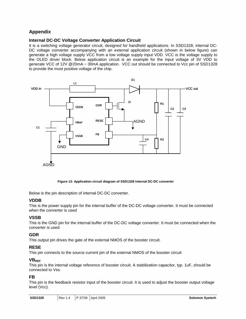
Internal DC-DC Voltage Converter Application Circuit It is a switching voltage generator circuit, designed for handheld applications. In SSD1328, internal DC-DC voltage converter accompanying with an external application circuit (shown in below figure) can generate a high voltage supply VCC from a low voltage supply input VDD. VCC is the voltage supply to the OLED driver block. Below application circuit is an example for the input voltage of 3V VDD to generate VCC of 12V @20mA ~ 30mA application. VCC out should be connected to Vcc pin of SSD1328 to provide the most positive voltage of the chip.
Below is the pin
VDDB This is the powwhen the conve
VSSB This is the GNDconverter is us
GDR This output pin
RESE This pin conne
VBREF This pin is the connected to V
FB This pin is the level (Vcc).
RESE
GDR
FB
VBref
VDDB
VSSB
VDD in L1
R1
R2
C2
C1
D1
J1
VCC out
C3
C4
RESE
GDR
FB
VBref
VDDB
VSSB
VDD in L1
R1
R2
C2
C1
D1
J1
VCC out
C3
C4
AGND
GND
AGND
r
Figure 13- Application circuit diagram of SSD1328 internal DC-DC converteRev 1.4 P 37/39 April 2005 Solomon Systech
description of internal DC-DC converter.
er supply pin for the internal buffer of the DC-DC voltage converter. It must be connected rter is used
pin for the internal buffer of the DC-DC voltage converter. It must be connected when the ed
drives the gate of the external NMOS of the booster circuit.
cts to the source current pin of the external NMOS of the booster circuit
internal voltage reference of booster circuit. A stabilization capacitor, typ. 1uF, should be ss.
feedback resistor input of the booster circuit. It is used to adjust the booster output voltage
Solomon Systech April 2005 P 38/39 Rev 1.4 SSD1328
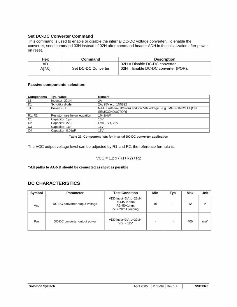
Set DC-DC Converter Command This command is used to enable or disable the internal DC-DC voltage converter. To enable the converter, send command 03H instead of 02H after command header ADH in the initialization after power on reset.
Hex Command Description AD
A[7:0]
Set DC-DC Converter 02H = Disable DC-DC converter. 03H = Enable DC-DC converter (POR).
Passive components selection:
Components Typ. Value Remark L1 Inductor, 22µH 2A D1 Schottky diode 2A, 25V e.g. 1N5822 J1 Power FET N-FET with low rDS(on) and low Vth voltage. e.g. MGSF1N02LT1 [ON
SEMICONDUCTOR] R1, R2 Resistor, see below equation 1%,1/4W C1 Capacitor, 1µF 16V C2 Capacitor, 22µF Low ESR, 25V C3 Capacitor, 1µF 16V C4 Capacitor, 0.01µF 16V
Table 22- Component lists for internal DC-DC converter application
The VCC output voltage level can be adjusted by R1 and R2, the reference formula is:
VCC = 1.2 x (R1+R2) / R2 *All paths to AGND should be connected as short as possible
DC CHARACTERISTICS
Symbol Parameter Test Condition Min Typ Max Unit
Vcc
DC-DC converter output voltage
VDD input=3V, L=22uH; R1=450Kohm; R2=50Kohm;
Icc = 20mA(loading)
10 - 12 V
Pwr DC-DC converter output power VDD input=3V, L=22uH; Vcc = 12V - - 400 mW
SSD1328 Rev 1.4 P 39/39 April 2005 Solomon Systech
Solomon Systech reserves the right to make changes without further notice to any products herein. Solomon Systech makes no warranty, representation or guarantee regarding the suitability of its products for any particular purpose, nor does Solomon Systech assume any liability arising out of the application or use of any product or circuit, and specifically disclaims any and all liability, including without limitation consequential or incidental damages. “Typical” parameters can and do vary in different applications. All operating parameters, including “Typicals” must be validated for each customer application by customer’s technical experts. Solomon Systech does not convey any license under its patent rights nor the rights of others. Solomon Systech products are not designed, intended, or authorized for use as components in systems intended for surgical implant into the body, or other applications intended to support or sustain life, or for any other application in which the failure of the Solomon Systech product could create a situation where personal injury or death may occur. Should Buyer purchase or use Solomon Systech products for any such unintended or unauthorized application, Buyer shall indemnify and hold Solomon Systech and its offices, employees, subsidiaries, affiliates, and distributors harmless against all claims, costs, damages, and expenses, and reasonable attorney fees arising out of, directly or indirectly, any claim of personal injury or death associated with such unintended or unauthorized use, even if such claim alleges that Solomon Systech was negligent regarding the design or manufacture of the part. http://www.solomon-systech.com