Embed Size (px)
Citation preview

Some Trends and Impacts of Micro/Nanoelectronics
G.Q. (Kouchi) ZhangPhilips Semiconductors
Delft University of [email protected]
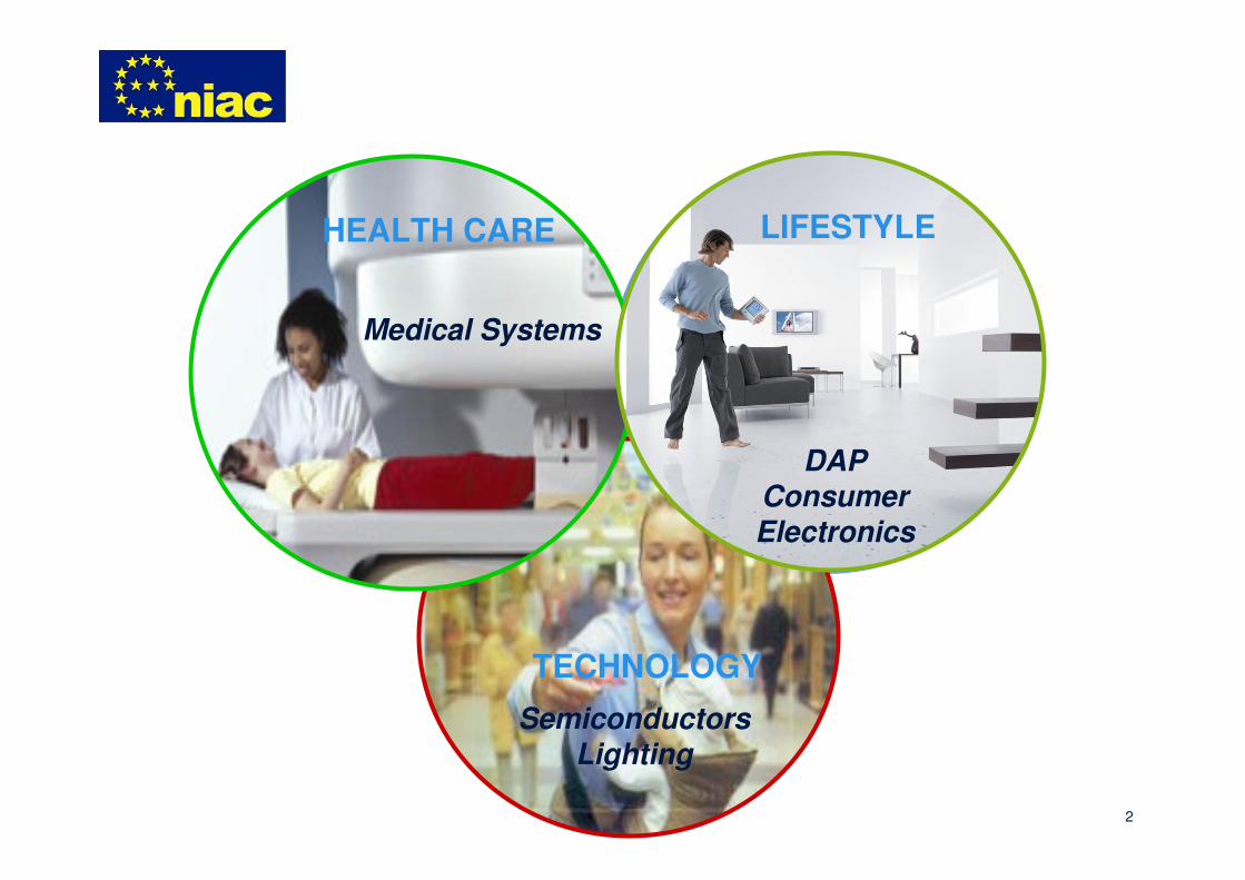
2
TECHNOLOGY
Medical Systems
DAPConsumerElectronics
SemiconductorsLighting
LIFESTYLEHEALTH CARE
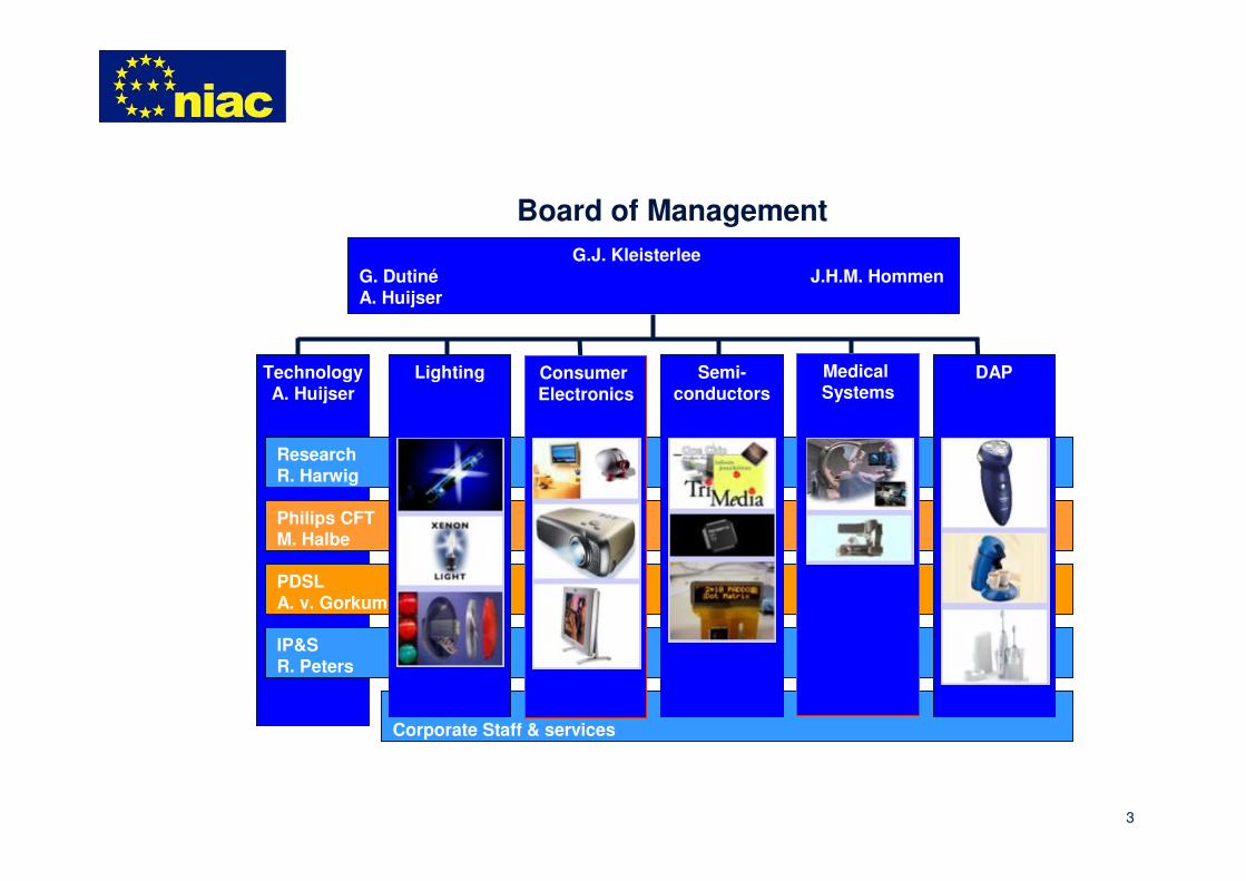
3
TechnologyA. Huijser
Corporate Staff & services
PDSLA. v. Gorkum
IP&SR. Peters
ResearchR. Harwig
G.J. Kleisterlee G. Dutiné J.H.M. HommenA. Huijser
Philips CFTM. Halbe
Lighting Semi-conductors
DAPConsumer Electronics
Medical Systems
Board of Management

4
Philips today Sales per sector, as % of total
1998 2003
100%= EUR 30.5 B 100%= EUR 29.0 B
UnallocatedLighting CE DAP Components Semiconductors Medical Misc.
36%
6%
14%
11%
6%8% 15%
4%16%
31%
7%
17%
21%
8%
5
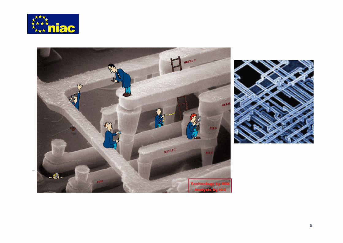
Bond Pad Via PlugMetal
Front-End
Back-End
6
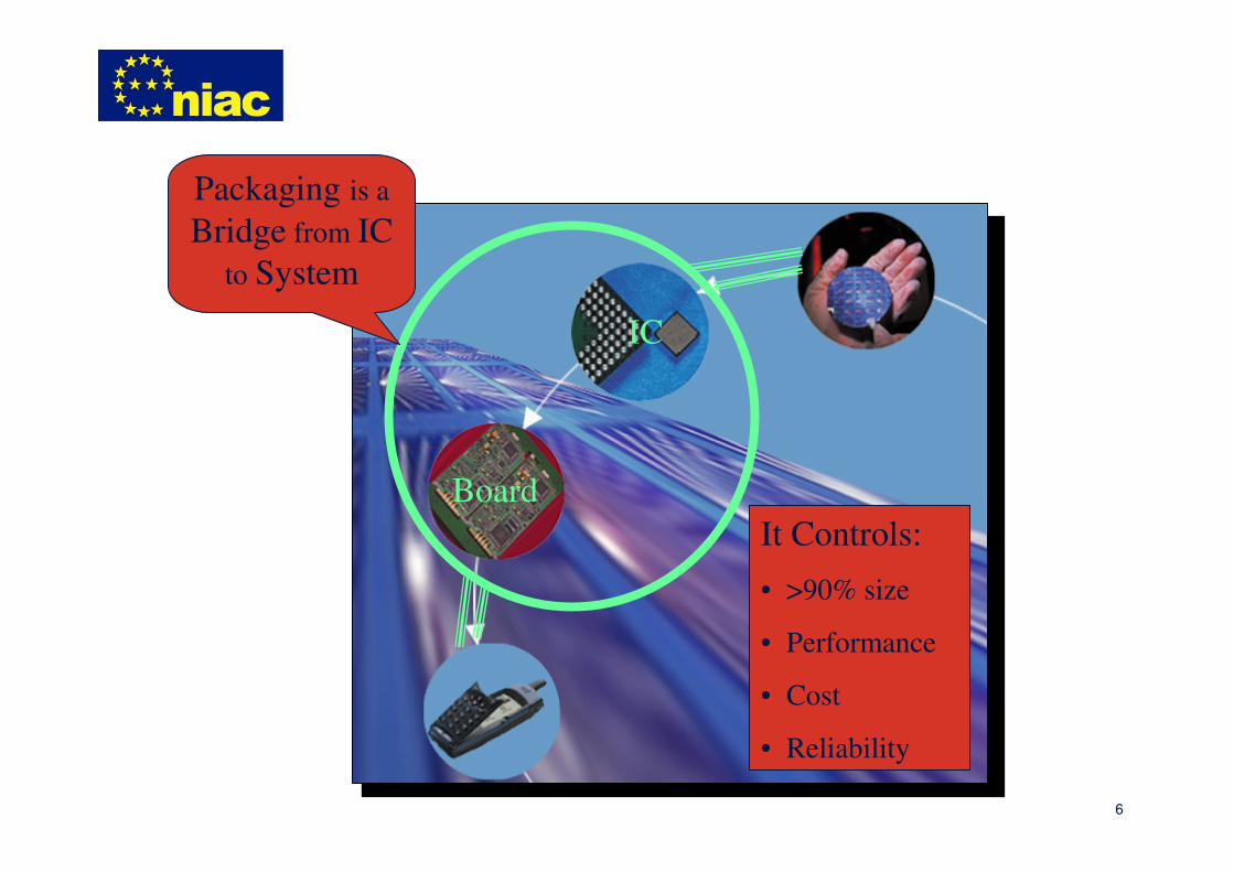
Board
IC
Packaging is a
Bridge from IC
to System
It Controls:
• >90% size
• Performance
• Cost
• Reliability
7
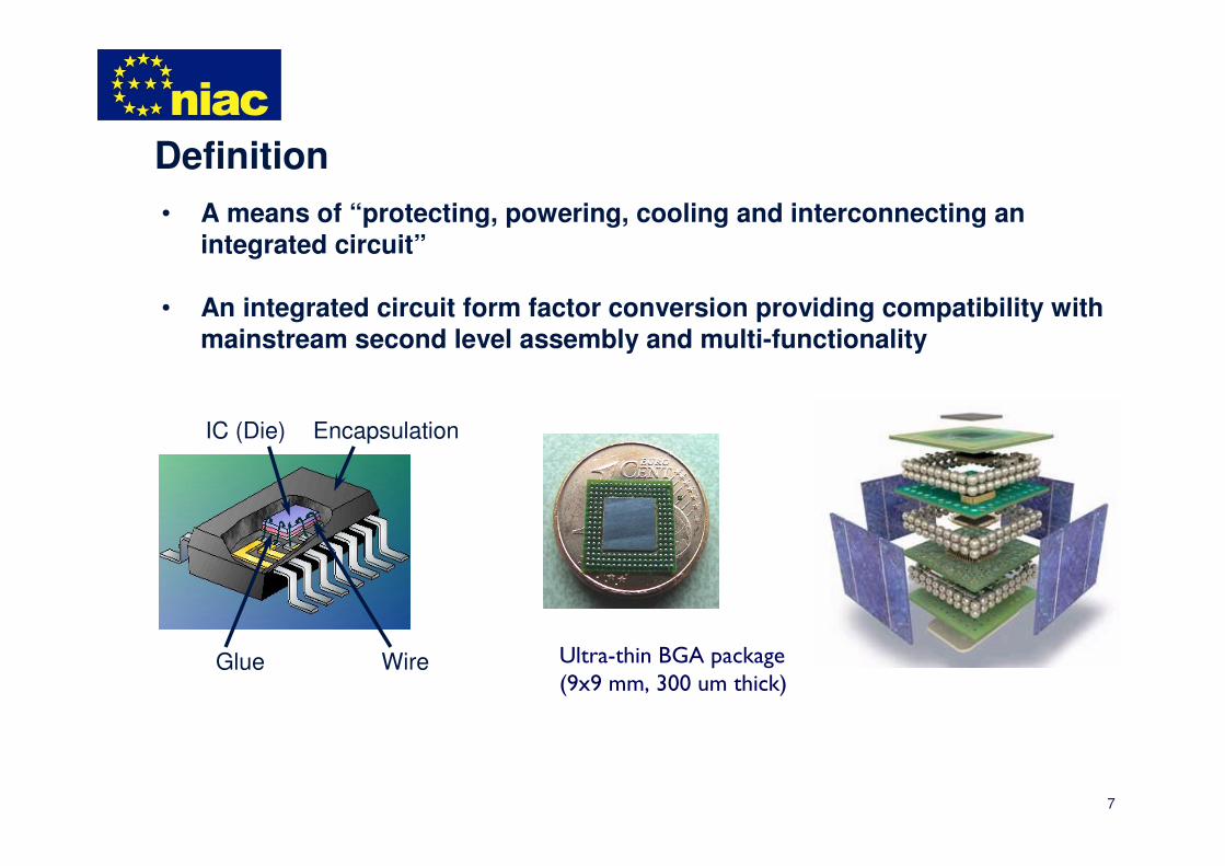
Definition
• A means of “protecting, powering, cooling and interconnecting an integrated circuit”
• An integrated circuit form factor conversion providing compatibility with mainstream second level assembly and multi-functionality
EncapsulationIC (Die)
Glue Wire Ultra-thin BGA package(9x9 mm, 300 um thick)
8
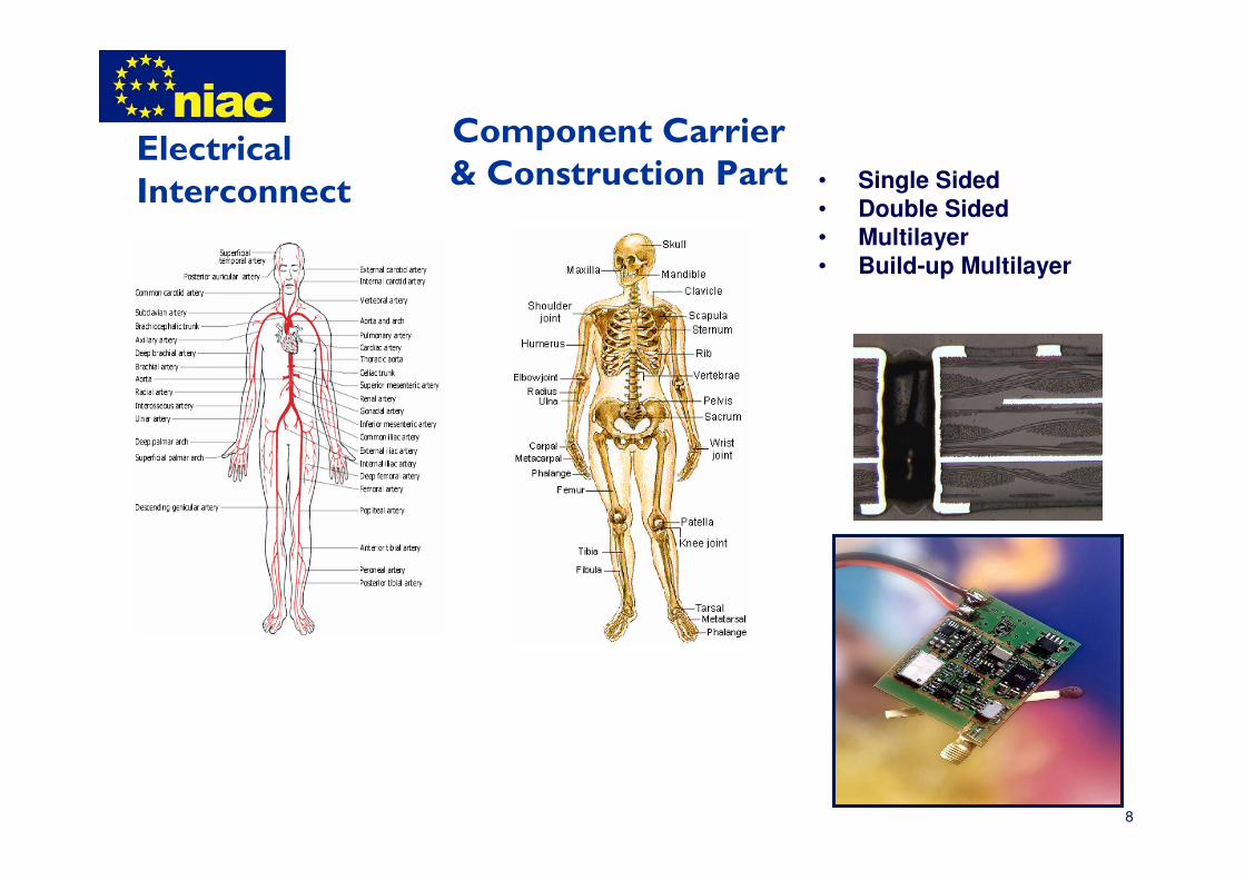
Electrical Interconnect
Component Carrier& Construction Part • Single Sided
• Double Sided• Multilayer• Build-up Multilayer
9
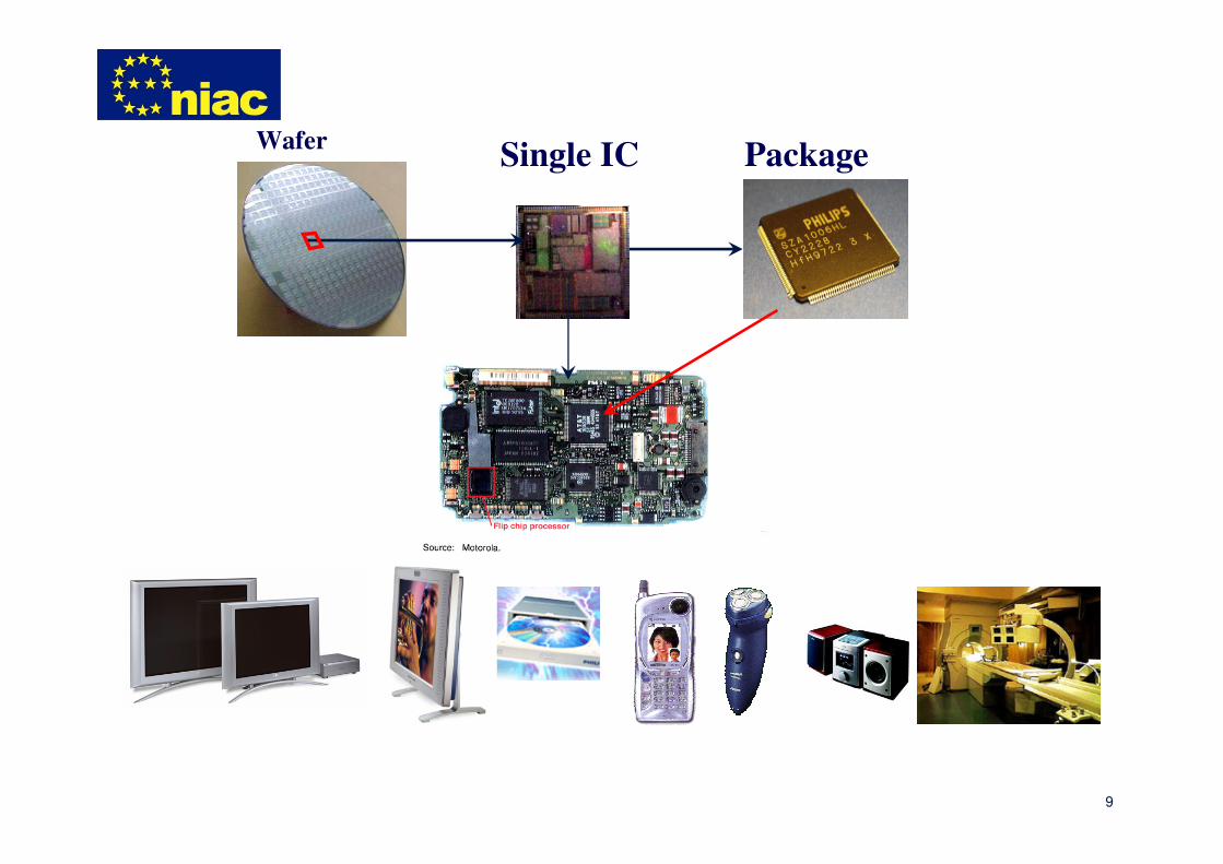
WaferPackageSingle IC
Some Trends and Impacts of Micro/Nanoelectronics
G.Q. (Kouchi) ZhangPhilips Semiconductors
Delft University of [email protected]
11
Outline
1. Development trends
2. Characteristics and Consequences
3. Challenges
4. Eniac /7FP
5. Concluding remarks
12
1. Development trends

13
14
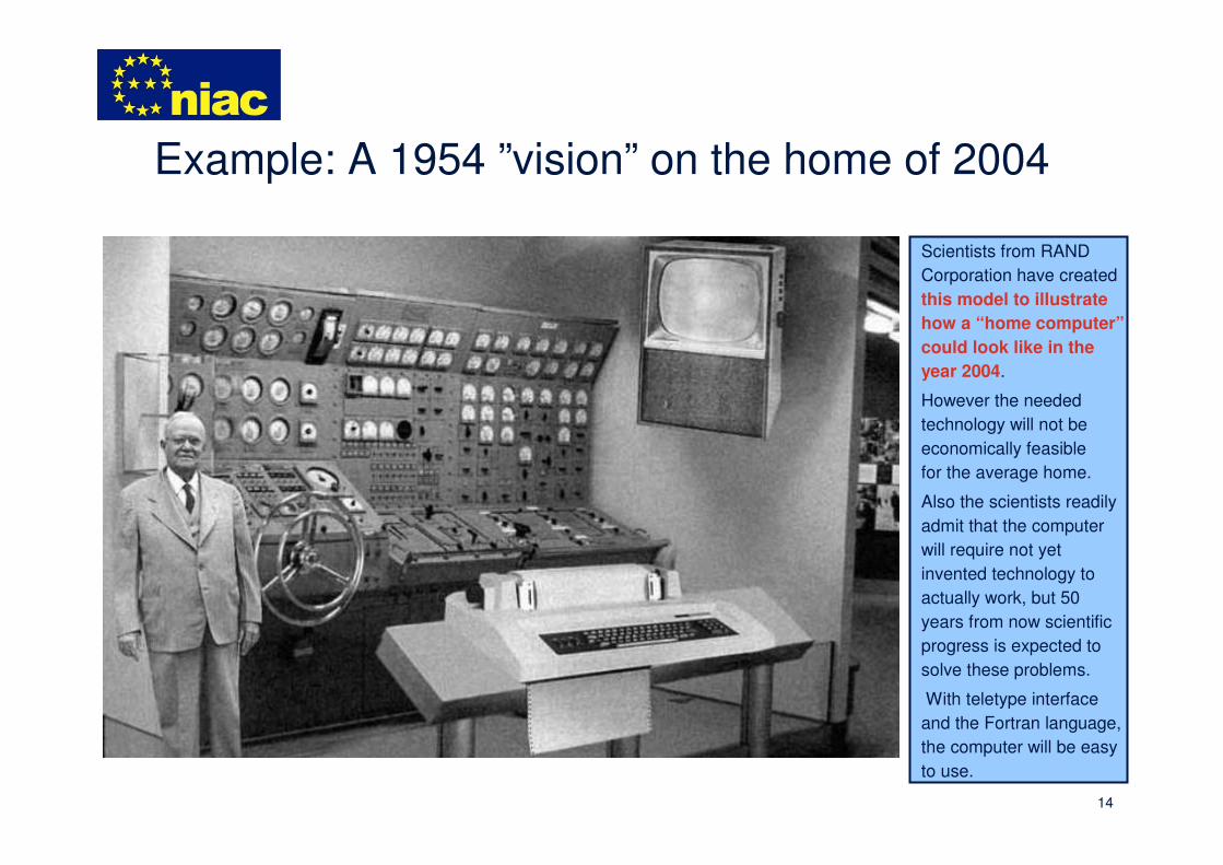
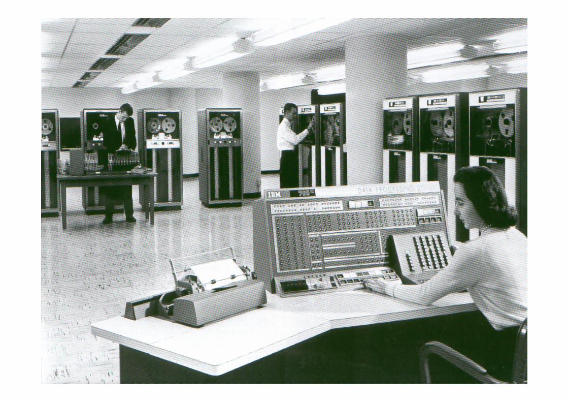
Example: A 1954 ”vision” on the home of 2004
Scientists from RAND
Corporation have created
this model to illustrate
how a “home computer”
could look like in the
year 2004.
However the needed
technology will not be
economically feasible
for the average home.
Also the scientists readily
admit that the computer
will require not yet
invented technology to
actually work, but 50
years from now scientific
progress is expected to
solve these problems.
With teletype interface
and the Fortran language,
the computer will be easy
to use.
15
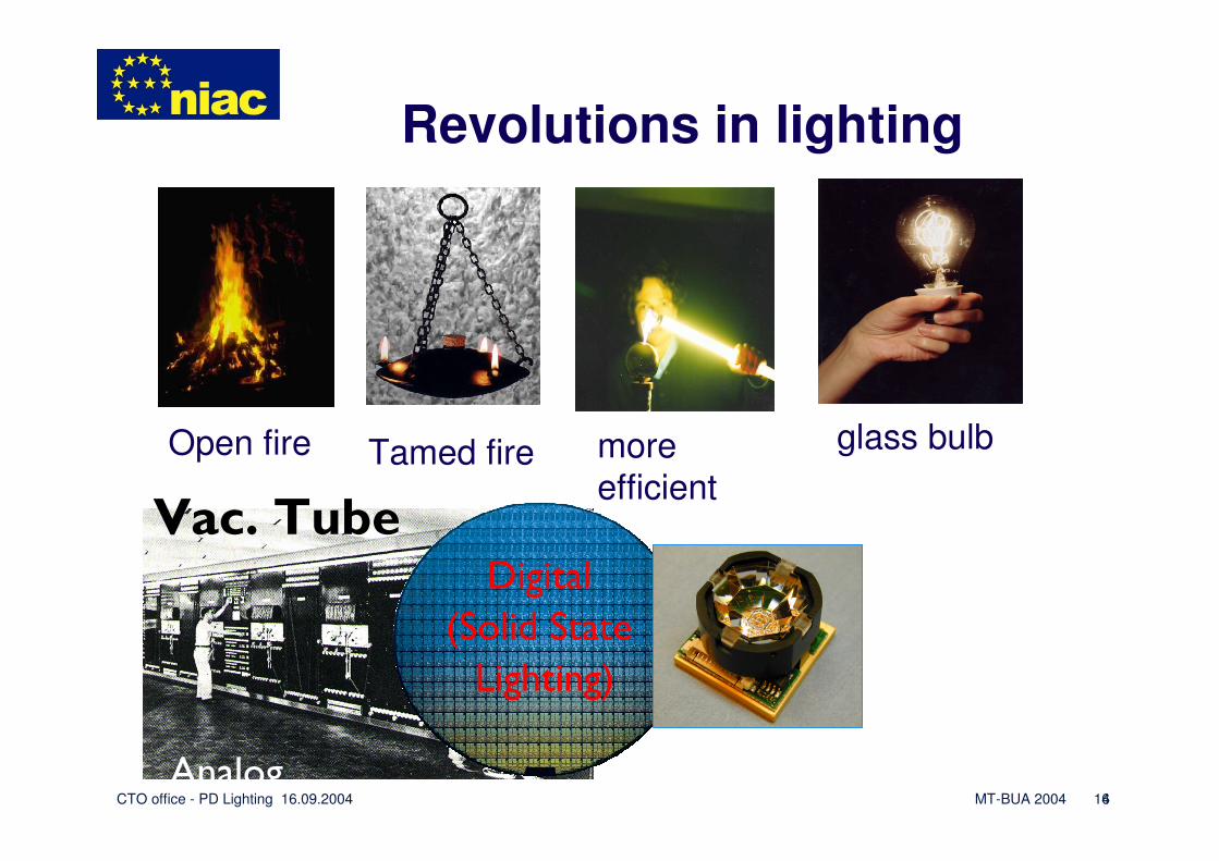
16MT-BUA 2004 4CTO office - PD Lighting 16.09.2004
Revolutions in lighting
Open fire Tamed fire glass bulbmore
efficient Vac. Tube
Analog
Digital
(Solid State
Lighting)
17
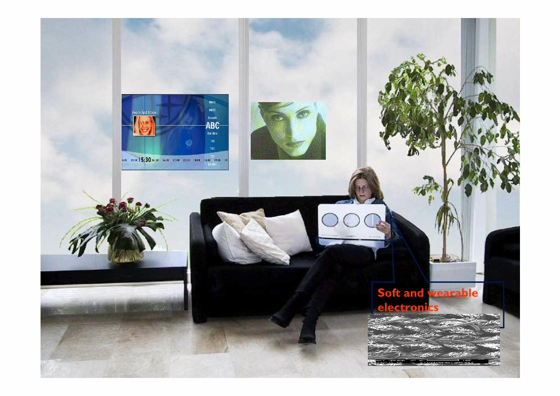
18
Soft and wearable electronics
19
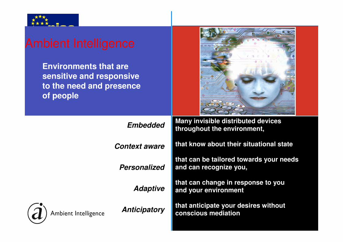
Embedded
Context aware
Personalized
Adaptive
Anticipatory
Many invisible distributed devices throughout the environment,
that know about their situational state
that can be tailored towards your needs and can recognize you,
that can change in response to you and your environment
that anticipate your desires without conscious mediation
Ambient Intelligence
Environments that are sensitive and responsive to the need and presence of people
20
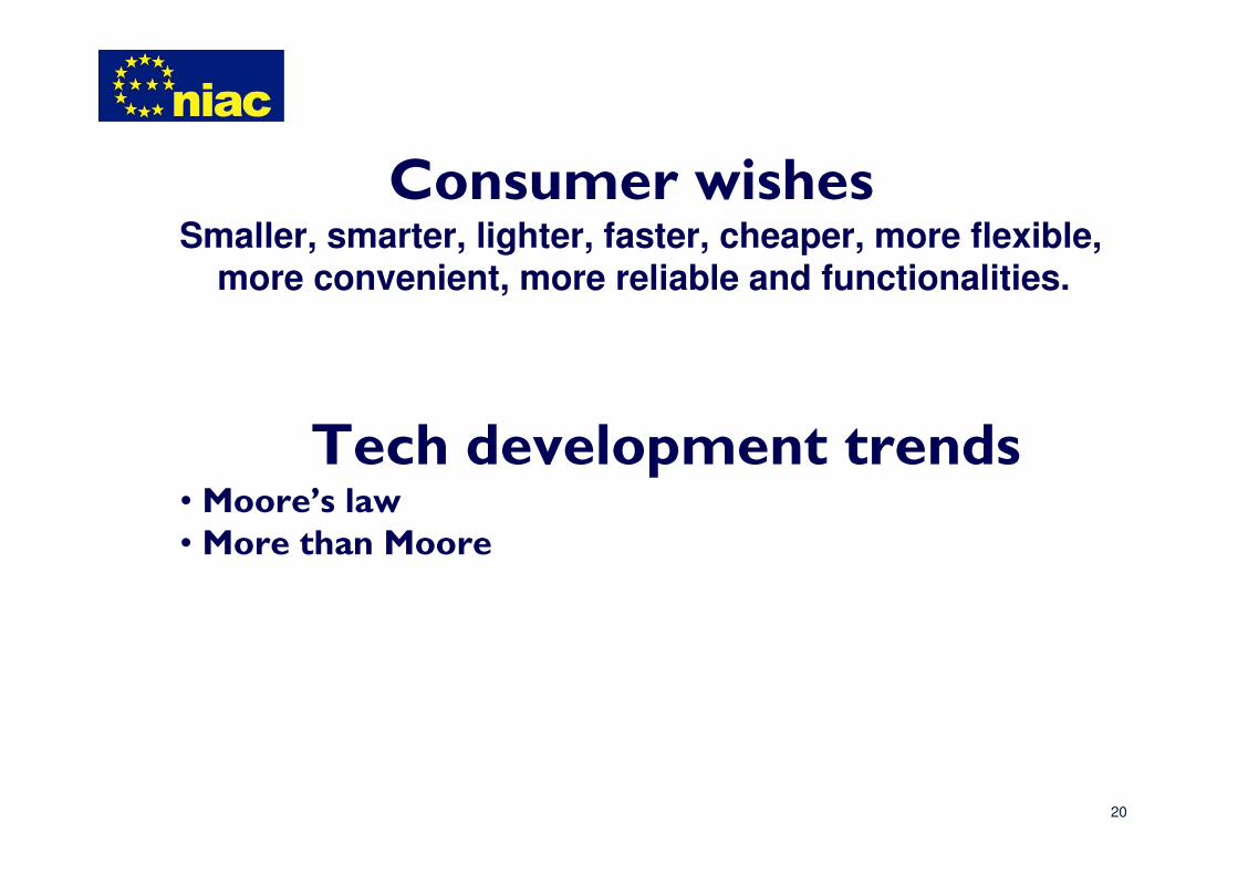
Consumer wishesSmaller, smarter, lighter, faster, cheaper, more flexible,
more convenient, more reliable and functionalities.
Tech development trends • Moore’s law• More than Moore
21
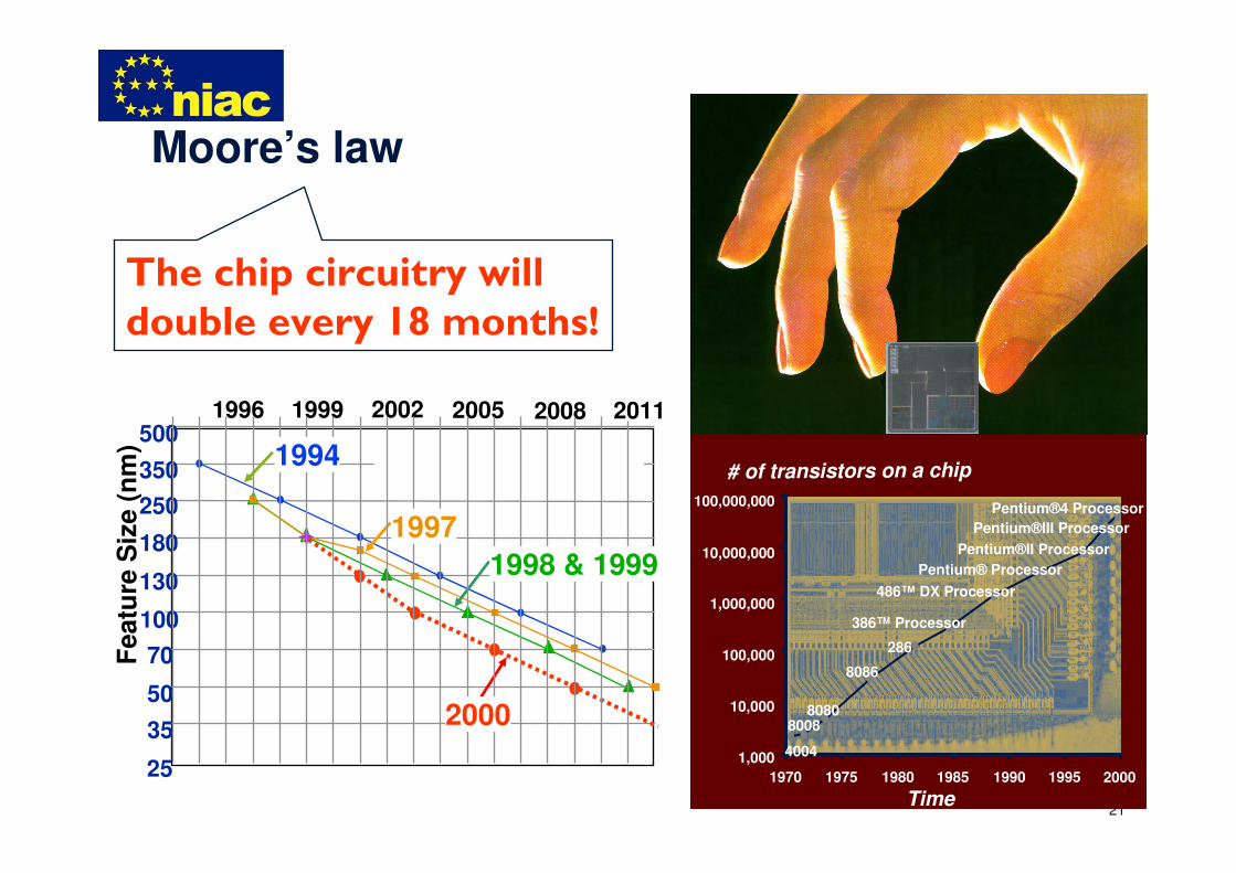
The ongoing miniaturizationallows integration of electronics
into peoples’ environments
4004
80088080
8086
286
386™ Processor
486™ DX Processor
Pentium® Processor
Pentium®II Processor
Pentium®III Processor
Pentium®4 Processor
1970 1975 1980 1985 1990 1995 2000
# of transistors on a chip
100,000,000
10,000,000
1,000,000
100,000
10,000
1,000
Time
Moore’s law
The chip circuitry will double every 18 months!
1996 1999 2002 2005 2008 2011
Featu
re S
ize (
nm
)500
350
250
180
130
100
70
50
35
25
1994
1997
1998 & 1999
2000
22
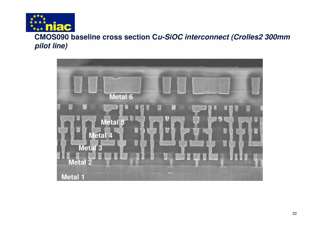
CMOS090 baseline cross section Cu-SiOC interconnect (Crolles2 300mm
pilot line)
Metal 6
Metal 1
Metal 2
Metal 3
Metal 4
Metal 5
23
Packaging & assembly
•Wire diameter < 10 microns•Interconnect pitch of NLWSP < 20 microns•Thickness of copper film/PCB < 5 microns•Microvia diameter < 20 microns•Wafer thickness < 40 microns
Not only the wafer technology, packaging and assembly are also going beyond visualization!
24
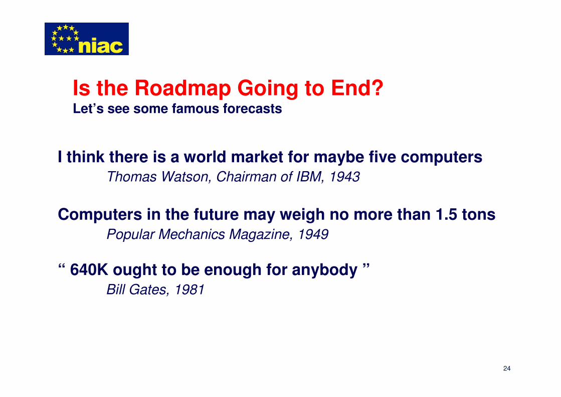
Is the Roadmap Going to End?Let’s see some famous forecasts
I think there is a world market for maybe five computers Thomas Watson, Chairman of IBM, 1943
Computers in the future may weigh no more than 1.5 tons Popular Mechanics Magazine, 1949
“ 640K ought to be enough for anybody ”Bill Gates, 1981
25
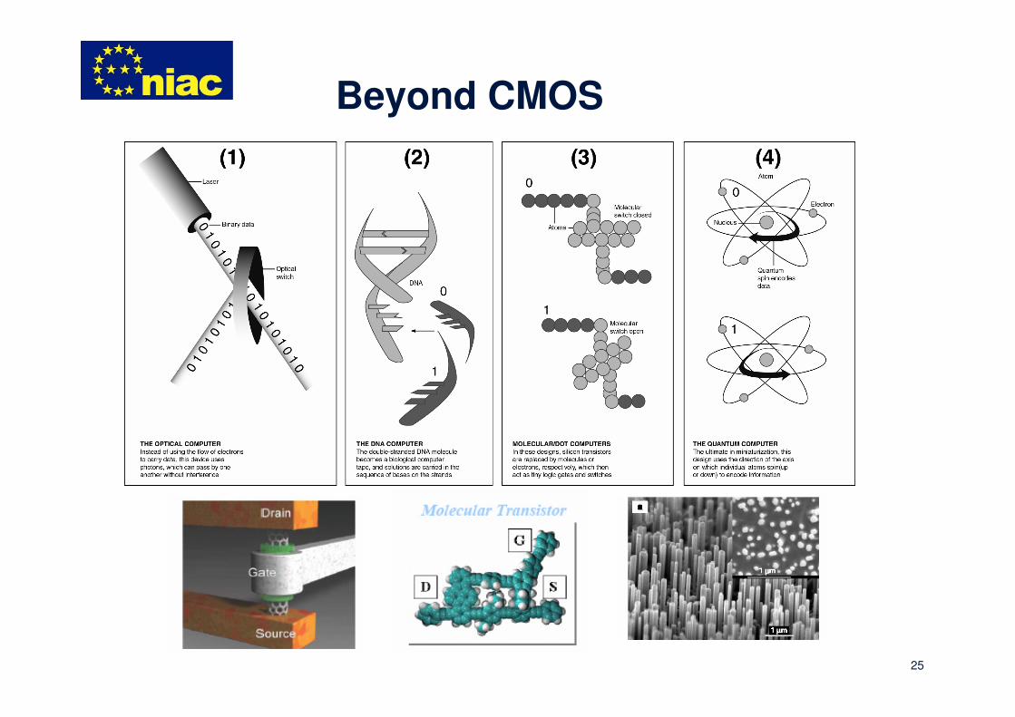
Beyond CMOS
26
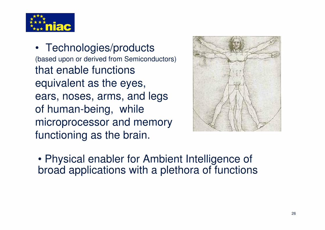
• Technologies/products (based upon or derived from Semiconductors)
that enable functions
equivalent as the eyes,
ears, noses, arms, and legs
of human-being, while
microprocessor and memory
functioning as the brain.
• Physical enabler for Ambient Intelligence ofbroad applications with a plethora of functions
27
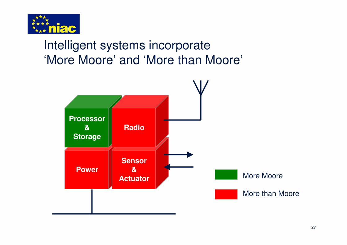
PowerSensor
&Actuator
Intelligent systems incorporate
‘More Moore’ and ‘More than Moore’
Processor&
StorageRadio
More Moore
More than Moore
28
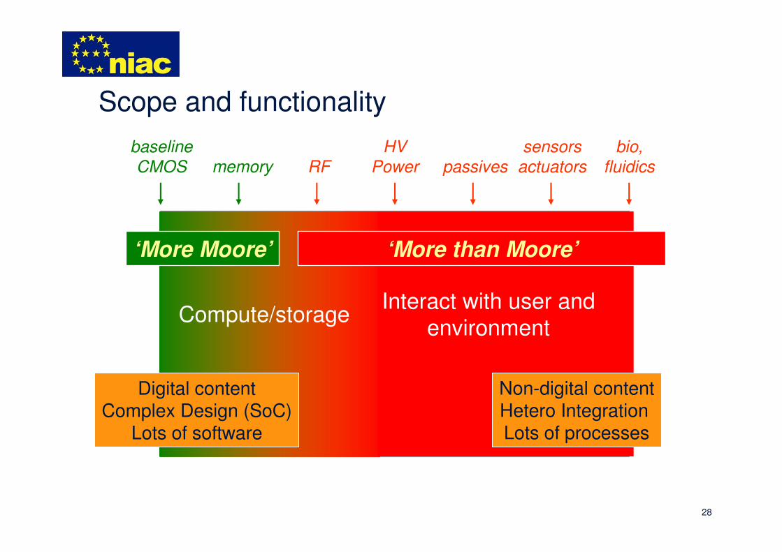
baseline
CMOS memory
Interact with user and environment
RF
HV
Power passives
sensors
actuators
bio,
fluidics
Compute/storage
‘More Moore’ ‘More than Moore’
Digital contentComplex Design (SoC)
Lots of software
Non-digital contentHetero Integration Lots of processes
Scope and functionality
29
9
ABS
Window Wipers
Steering angle
Oil Level and aging
Oil Temperature
Steering Torsion
EPAS Motor Positioning
Engine Coolant
E-Throttle
VVT
Active Transmission
n
Chassis Height
Mirror Positioning
CAM / CRANK
Butterfly Valve
Headlight Adjustment Sidewall
Torsion
EHB / EMB
Seat Positioning
E-Gas
Tire pressure
Monitor
30
Intelligence applied: personal comfort
Personal Health Monitor-Heart activity
-Blood pressure
-Glucose level
Identification
Mouse
Decibel Meter
Personal Weather Station-Humidity
-Pressure
-Ozone
-UV exposure
Gaming
Personal Map-Compass
-GPS
-Altitude
31
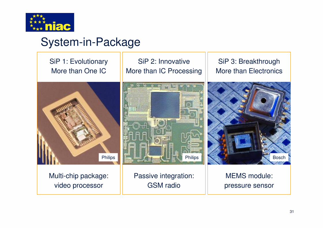
System-in-Package
SiP 1: Evolutionary
More than One IC
Multi-chip package:
video processor
SiP 2: Innovative
More than IC Processing
Passive integration:
GSM radio
SiP 3: Breakthrough
More than Electronics
MEMS module:
pressure sensor
Philips Philips Bosch
32
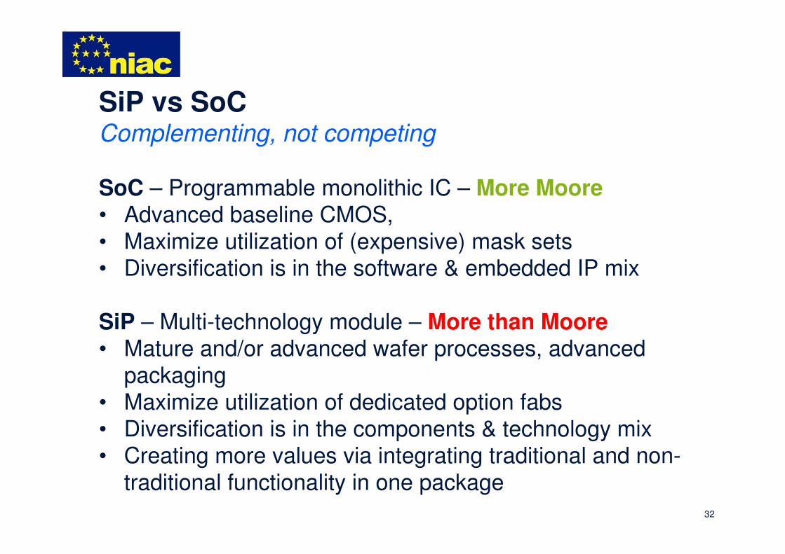
SiP vs SoCComplementing, not competing
SoC – Programmable monolithic IC – More Moore• Advanced baseline CMOS,
• Maximize utilization of (expensive) mask sets• Diversification is in the software & embedded IP mix
SiP – Multi-technology module – More than Moore• Mature and/or advanced wafer processes, advanced
packaging• Maximize utilization of dedicated option fabs
• Diversification is in the components & technology mix• Creating more values via integrating traditional and non-
traditional functionality in one package
33
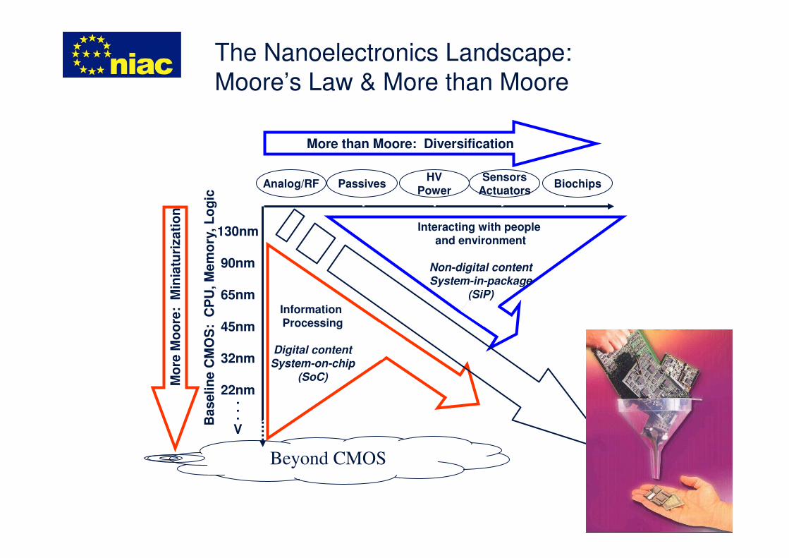
More than Moore: Diversification
Mo
re M
oo
re:
Min
iatu
rizati
on
Baseli
ne C
MO
S:
CP
U, M
em
ory
, L
og
ic
BiochipsSensors
ActuatorsHV
PowerAnalog/RF Passives
130nm
90nm
65nm
45nm
32nm
22nm...V
Information Processing
Digital contentSystem-on-chip
(SoC)
Interacting with people and environment
Non-digital contentSystem-in-package
(SiP)
Beyond CMOS
The Nanoelectronics Landscape:
Moore’s Law & More than Moore
Combining SoC and SiP: High Value System
s
34
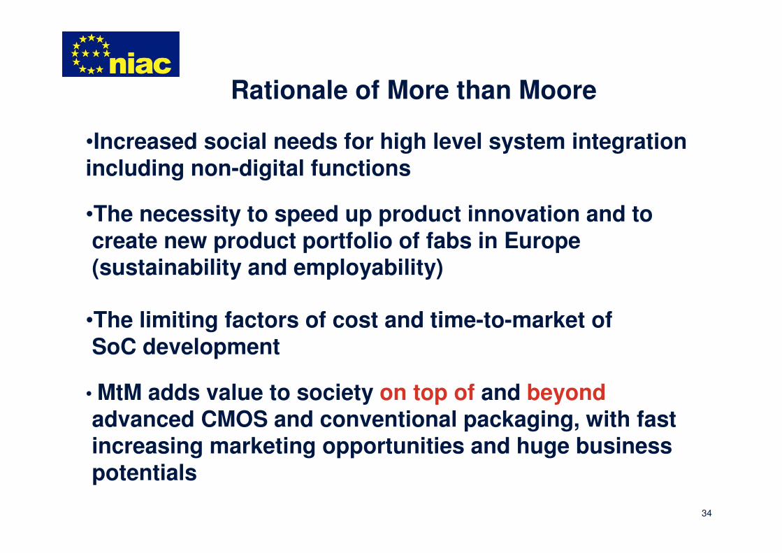
• MtM adds value to society on top of and beyondadvanced CMOS and conventional packaging, with fast increasing marketing opportunities and huge business potentials
•The necessity to speed up product innovation and to create new product portfolio of fabs in Europe(sustainability and employability)
•The limiting factors of cost and time-to-market of SoC development
•Increased social needs for high level system integrationincluding non-digital functions
Rationale of More than Moore
35
2. Characteristics and Consequences
36
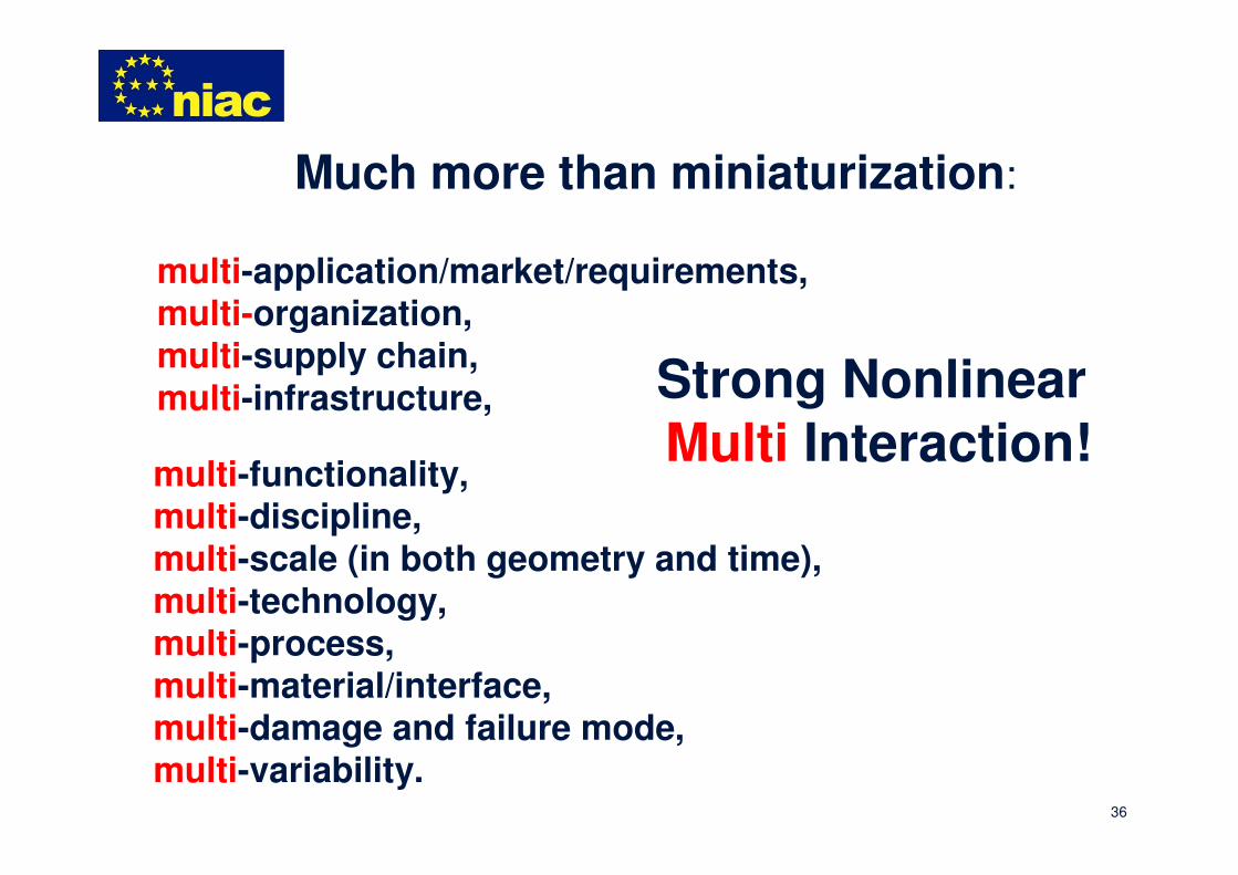
multi-application/market/requirements, multi-organization, multi-supply chain,multi-infrastructure,
Much more than miniaturization:
multi-functionality, multi-discipline, multi-scale (in both geometry and time), multi-technology,multi-process, multi-material/interface, multi-damage and failure mode,multi-variability.
Strong Nonlinear Multi Interaction!
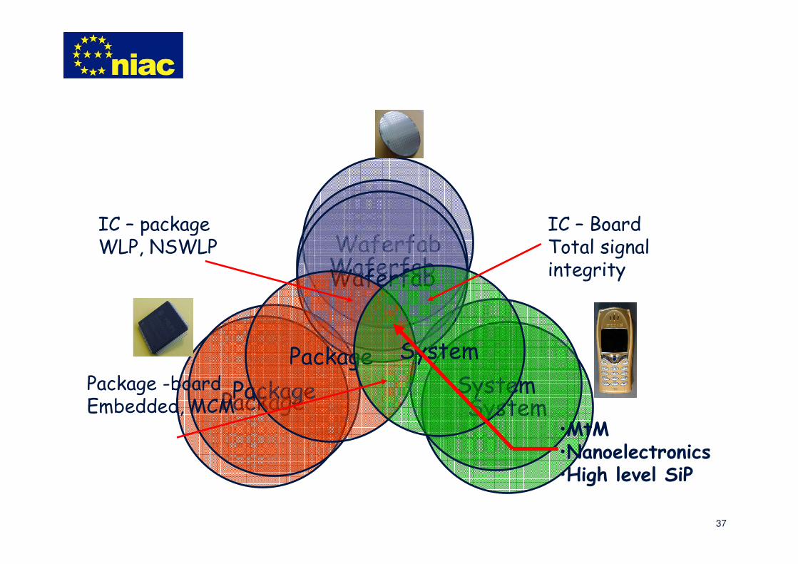
37
Waferfab
Package System
Waferfab
Package System
Waferfab
Package System
IC – BoardTotal signalintegrity
IC – packageWLP, NSWLP
Package -boardEmbedded, MCM
•MtM•Nanoelectronics•High level SiP

38
Linking Giga-Scale Dreams to Nano-Scale Realities
?
Giga-Scale Complexity Nanoscale Realities
Dramatically increased design complexity
Architectural gapNanoscale design tolerance and process windowsDevice variability impacts predictability and yield
No co-designing theories, methods and tools
39
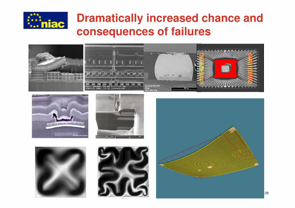
Buckling
Dramatically increased chance and consequences of failures
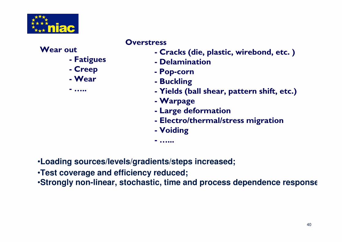
40
Overstress- Cracks (die, plastic, wirebond, etc. )- Delamination- Pop-corn- Buckling- Yields (ball shear, pattern shift, etc.)- Warpage - Large deformation- Electro/thermal/stress migration- Voiding- …...
Wear out- Fatigues- Creep- Wear- …..
•Loading sources/levels/gradients/steps increased;
•Test coverage and efficiency reduced;•Strongly non-linear, stochastic, time and process dependence responses;
41
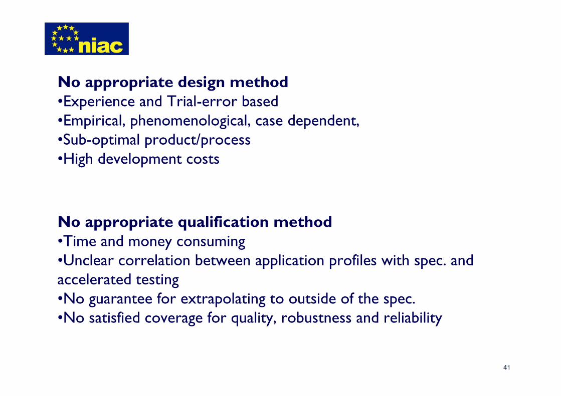
No appropriate design method•Experience and Trial-error based •Empirical, phenomenological, case dependent, •Sub-optimal product/process•High development costs
No appropriate qualification method •Time and money consuming•Unclear correlation between application profiles with spec. and accelerated testing•No guarantee for extrapolating to outside of the spec. •No satisfied coverage for quality, robustness and reliability
42
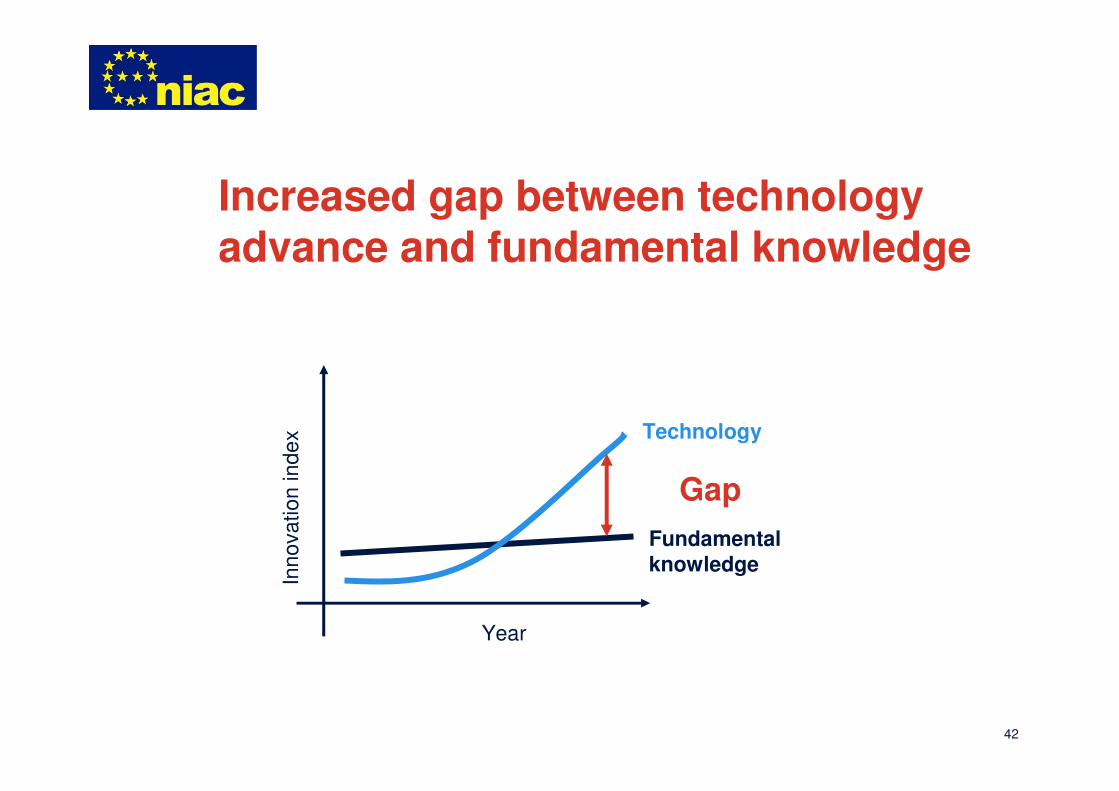
Increased gap between technology advance and fundamental knowledge
Fundamentalknowledge
Technology
Gap
Year
Inn
ova
tio
n in
de
x
43
3. Challenges- Predictive modeling
44
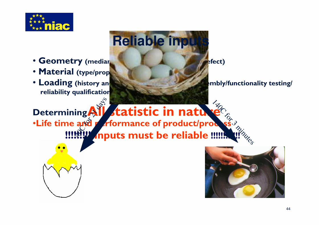
• Geometry (median value/distribution/tolerance/defect)
• Material (type/property/interface)
• Loading (history and gradients, manufacturing/assembly/functionality testing/
reliability qualifications/field use)
Determining•Life time and performance of product/process
!!!!!!!!! Inputs must be reliable !!!!!!!!!!!!
All statistic in nature
40C
for
21
days 140C
for 3 minutes
Reliable inputs
45
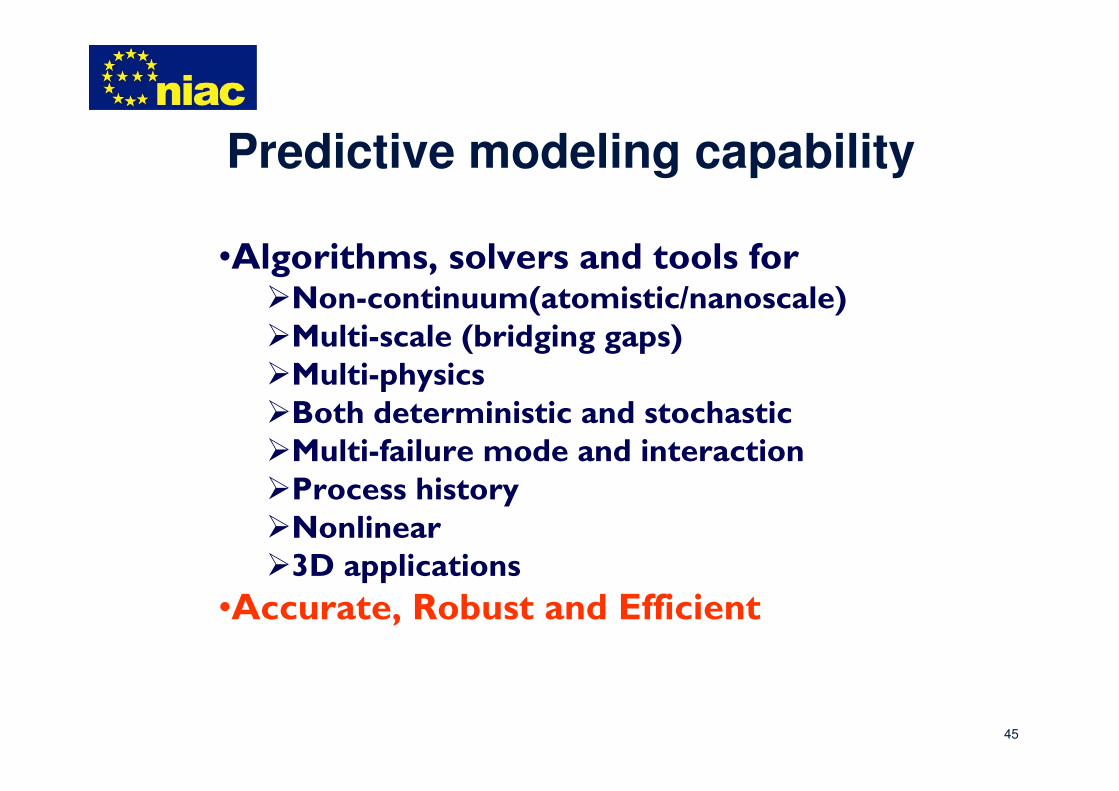
•Algorithms, solvers and tools for�Non-continuum(atomistic/nanoscale)�Multi-scale (bridging gaps)�Multi-physics�Both deterministic and stochastic�Multi-failure mode and interaction�Process history�Nonlinear�3D applications
•Accurate, Robust and Efficient
Predictive modeling capability
46
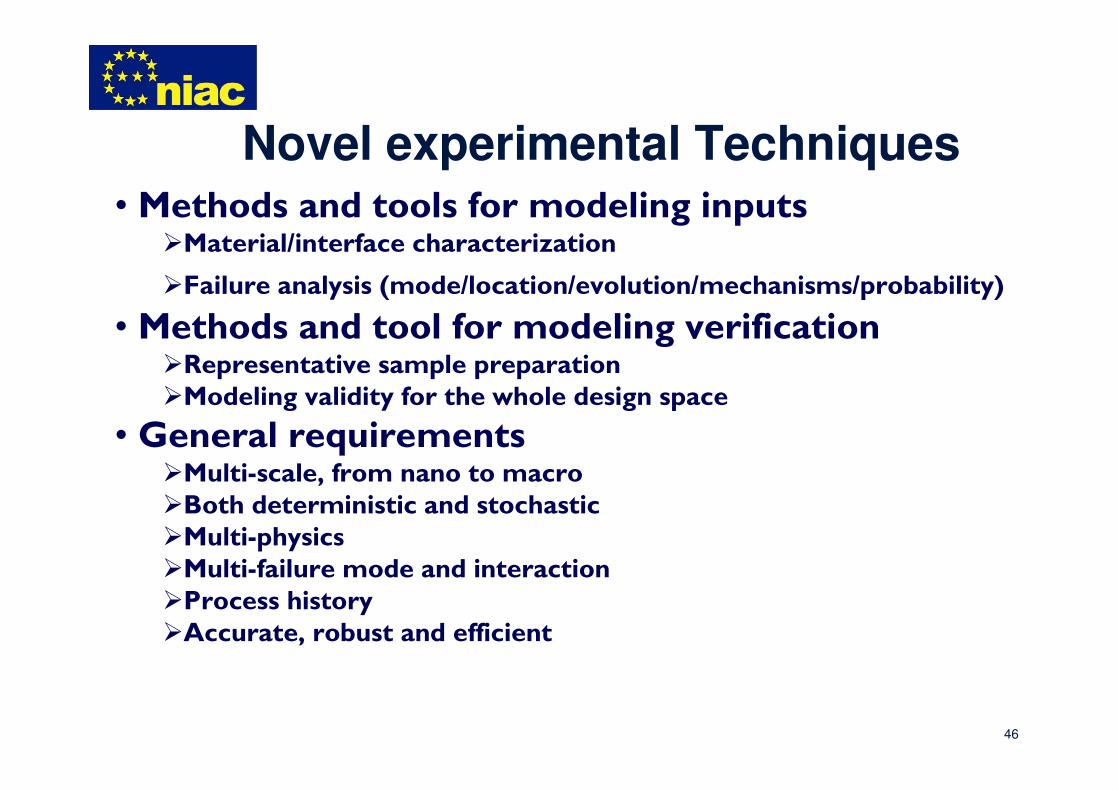
Novel experimental Techniques• Methods and tools for modeling inputs
�Material/interface characterization
�Failure analysis (mode/location/evolution/mechanisms/probability)
• Methods and tool for modeling verification�Representative sample preparation�Modeling validity for the whole design space
• General requirements �Multi-scale, from nano to macro�Both deterministic and stochastic�Multi-physics�Multi-failure mode and interaction�Process history�Accurate, robust and efficient
47
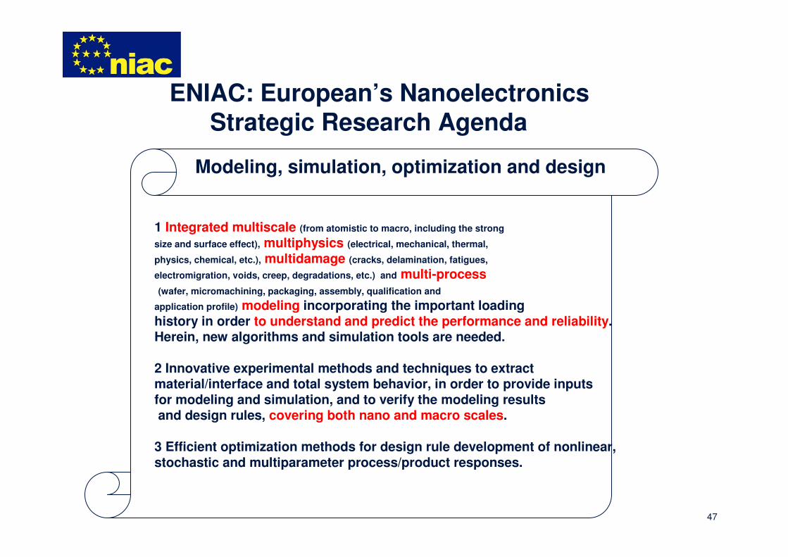
ENIAC: European’s Nanoelectronics Strategic Research Agenda
1 Integrated multiscale (from atomistic to macro, including the strong
size and surface effect), multiphysics (electrical, mechanical, thermal,
physics, chemical, etc.), multidamage (cracks, delamination, fatigues,
electromigration, voids, creep, degradations, etc.) and multi-process(wafer, micromachining, packaging, assembly, qualification and
application profile) modeling incorporating the important loading history in order to understand and predict the performance and reliability. Herein, new algorithms and simulation tools are needed.
2 Innovative experimental methods and techniques to extract material/interface and total system behavior, in order to provide inputs for modeling and simulation, and to verify the modeling resultsand design rules, covering both nano and macro scales.
3 Efficient optimization methods for design rule development of nonlinear, stochastic and multiparameter process/product responses.
Modeling, simulation, optimization and design
4. Eniac
European Technology Platform
European Nanoelectronics InitiativeAdvisory Council
49
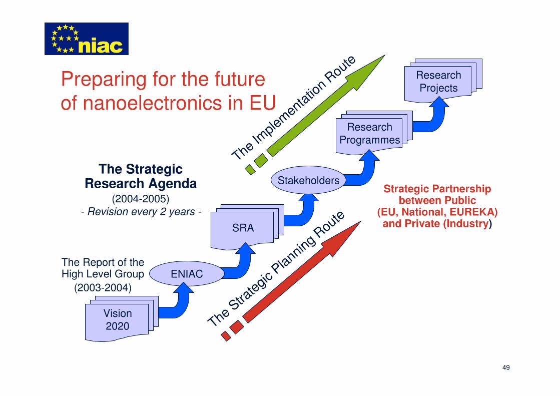
Preparing for the future
of nanoelectronics in EU
SRA
The Report of the High Level Group
(2003-2004)
The Strategic Research Agenda
(2004-2005)
- Revision every 2 years -
ENIAC
Vision
2020 The Stra
tegic
Plannin
g Route
Research
Projects
Research
Programmes
StakeholdersStrategic Partnership
between Public (EU, National, EUREKA) and Private (Industry)
The Imple
menta
tion R
oute
50
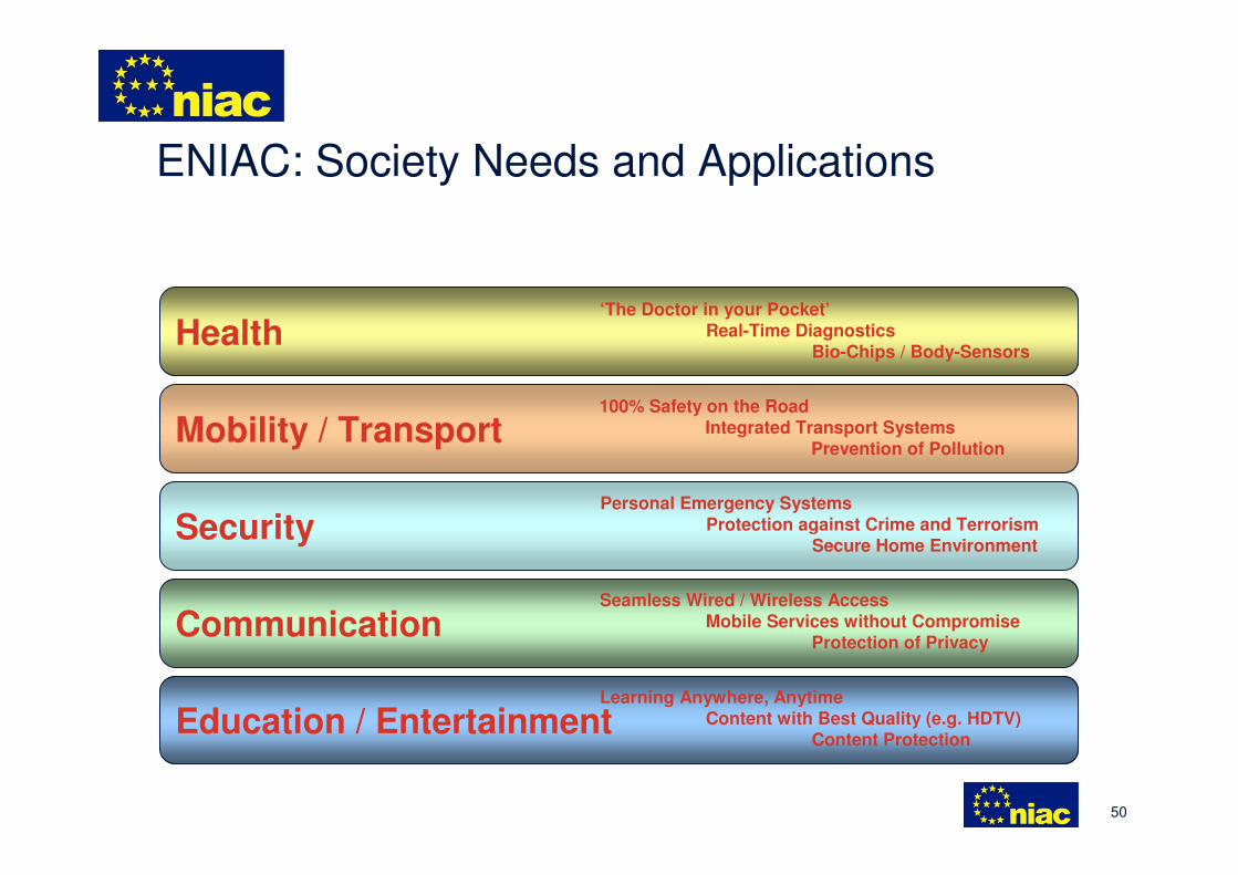
ENIAC: Society Needs and Applications
Mobility / Transport
Security
Health
Communication
Education / Entertainment
100% Safety on the RoadIntegrated Transport Systems
Prevention of Pollution
‘The Doctor in your Pocket’Real-Time Diagnostics
Bio-Chips / Body-Sensors
Personal Emergency SystemsProtection against Crime and Terrorism
Secure Home Environment
Seamless Wired / Wireless AccessMobile Services without Compromise
Protection of Privacy
Learning Anywhere, AnytimeContent with Best Quality (e.g. HDTV)
Content Protection

51
Six enabling technology domains
‘MoreMoore’
‘More than Moore’
Design Automation
Application Domains
Equipment and Materials
He
tero
ge
ne
ou
sIn
tegra
tion
Be
yo
nd
CM
OS
Society Needs
52
5. Concluding remark
53
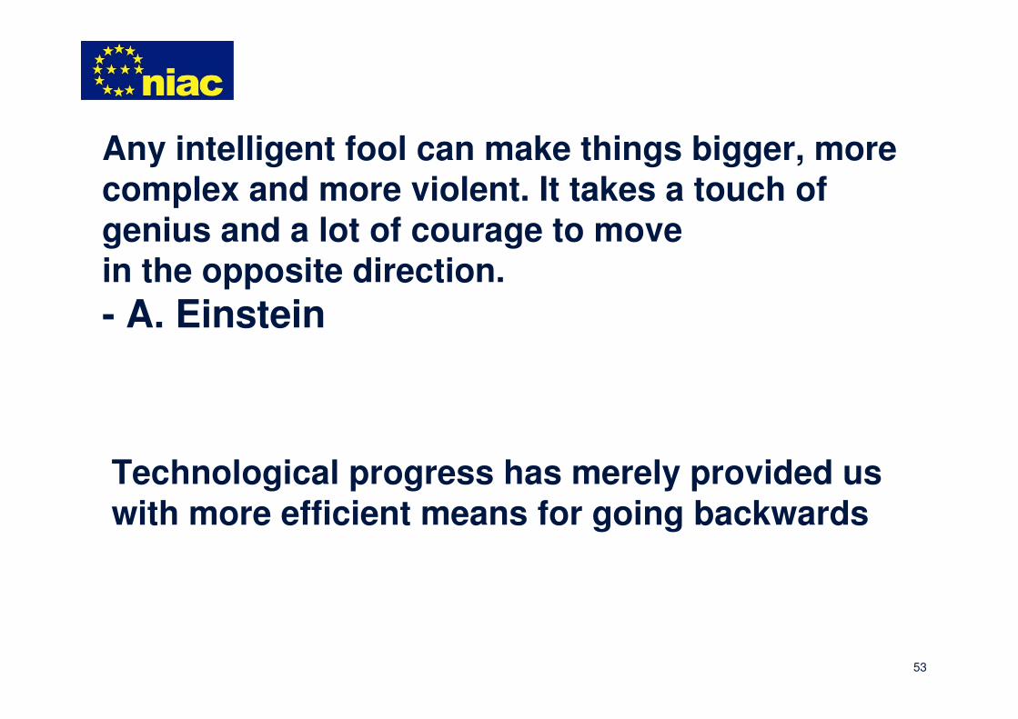
Any intelligent fool can make things bigger, more complex and more violent. It takes a touch of genius and a lot of courage to move in the opposite direction.
- A. Einstein
Technological progress has merely provided us with more efficient means for going backwards
54
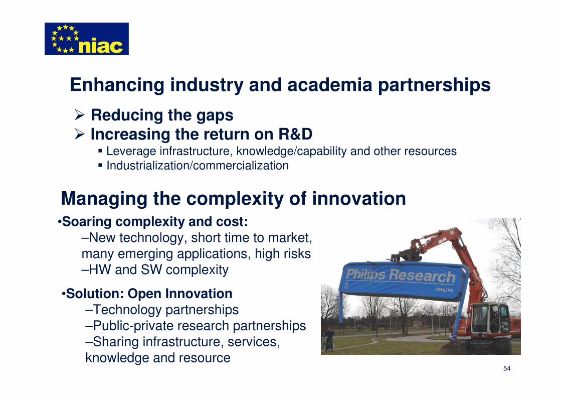
Enhancing industry and academia partnerships
� Reducing the gaps� Increasing the return on R&D
� Leverage infrastructure, knowledge/capability and other resources
� Industrialization/commercialization
Managing the complexity of innovation•Soaring complexity and cost:
–New technology, short time to market, many emerging applications, high risks–HW and SW complexity
•Solution: Open Innovation–Technology partnerships –Public-private research partnerships–Sharing infrastructure, services, knowledge and resource
552631-10-2005
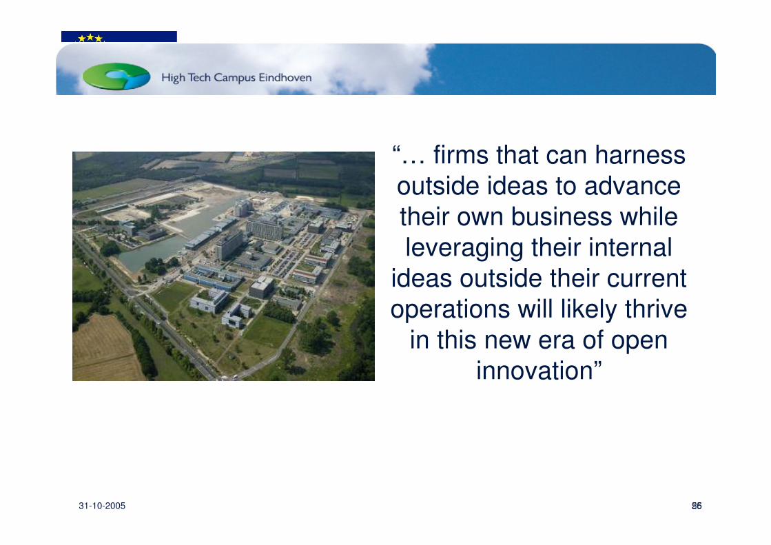
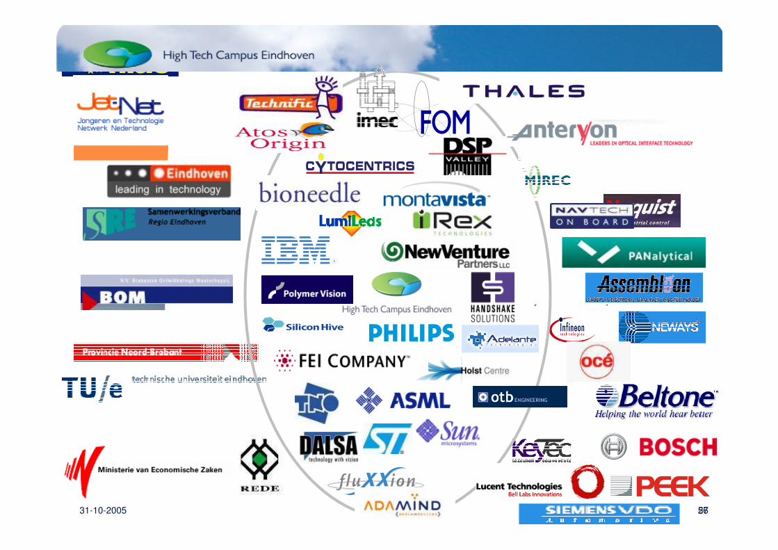
“… firms that can harness
outside ideas to advance
their own business while
leveraging their internal
ideas outside their current
operations will likely thrive
in this new era of open
innovation”
562731-10-2005

57
Thanks for your attention!
Questions?