Embed Size (px)
Citation preview

PI Paul Rothemund, computer scientist, Senior Research Associate (research faculty) Expert in creating complex shapes and patterns using DNA self-assembly. Interested in scaling up DNA self-assembly, bridging nano, micro and macro scales.
PI Erik Winfree, computer scientist, Associate Professor Expert in creating complex shapes and patterns using DNA self-assembly. Interested in creating large, complex patterns using algorithmic self-assembly.
PI Marc Bockrath, applied physicist, Assistant Professor Expert in nanoscale device fabrication, physics and properties of single molecules. Interested in carbon nanotube (CNT) circuit fabrication and characterization.
Hareem Maune, graduate student synthesizing and testing CNT devices
PI William Goddard, theoretical chemist, Full Professor Expert in atomistic simulation of chemical systems. Interested in simulation of DNA-CNT device and circuit systems.
Andres Jaramillo-Botero, Director Caltech Center for Multi-scale ModellingSiping Han, graduate student, synthesizing and modelling CNT devices metallization of DNA nanostructures.
Goal: To use DNA self-assembly to overcome the challengesof optical and e-beam lithography in creating nanoscale circuits.

100 nanometer shapes with 200 pixel patterns, 6 nanometer resolution,100 billion per drop, 90% yield (Rothemund)uses many distinct DNA strands, relatively expensive for higher complexity
100 nanometers200 nanometers
Arbitrary shapes Arbitrary patterns on top of shapes 100 nm100 nm

ATGGA GACCA
CTGGT TACCT
42 nucleotides, 14.3 nm
ATGGA GACCA
CTGGT TACCT
ATGGA GACCA
CTGGT TACCT
ATGGA GACCA
CTGGT TACCT
ATGGA GACCA
CTGGT TACCT
6 tile wideDNA ribbon:


Si/ SiO2
Pd
+
+
Challenge 1: "Functionalization" electronically or optically active materialsmust be coupled to DNA nanostructures in high yield at specificed locations.
We focus on carbon nanotubes (CNTs) but also work on metallization.
DNA noncovalently wraps CNTsand allows them to disperse inbuffer solution.
An origami is made with 'red' and'blue' DNA hooks, having differentDNA sequences on top and bottom.Two batches of CNTs are madewith complementary red or bluestrands.
Red and blue CNT assembleinto crossbar FET on theorigami.
A device measurement is made

To make nanostructures more rigid and to avoid aggregationorigami-ribbon hybrids are used.
crossbar
red tube blue tubes
50 nm
MOSFET geometry
ChannelGate
red and blue hooks

Over 30% of tubes are within 10 degrees of the desired orientation
Characterization of DNA self-assembled CNT FET
------ Vg= 0.5V
-- -- Vg= -0.5V-- - -- Vg= 0.5V
VSD [V]
I SD
[nA
]
Vg [V]
I SD [
nA
]
-0.5 0.0 0.5 1.00
100
200
300
400
-0.5 0.0 0.5
0
100
200
VSD = 0.85VISD
VSD
Vg
ab
ISD
Orientation of SWNT
0
5
10
15
20
25
30
35
40
0-20 20-40 40-60 60-80 80-100 100-120 120-140 140-160 160-180
22%2%
76%
Red side (-1)Unknown (0)Blue side (1)F
requ
ency
Angle

Challenges for DNA organized nanoelectronics 2

Challenge 3, "Wiring-up" and "Bridging length scales": DNA nanostructureshave a fundamental size mismatch with electronics at a larger spatial scale.
Still hard to build, we would liketo self-assemble connections.
E-beam cannot achieve wiring tocomplex objects at the nanoscale.
Challenge 4, "Scaling-up": 200 pixels for DNA origami is a start, butwe expect to want billions of devices. Similarly, a single FET is nice butwe desire circuits.
E-beam patterningcan only wire-upsimple nanodevices.
single origamimax 200 devices
VLSI chip


Rothemund's Aims:
To create DNA structures with features that bridge the nano andmicroscales so that a complete device can be fabricated...
To continue work with IBM, to replicate positioning andorienting work at Caltech, so that CNT devices can be moreeasily characterized and integrated.
To combine multiple origami to create large origami breadboards.
A
B
C
D
A B C D
jigsaw puzzle stacking bonds enable 800 pixels
origami shapespatterned DLC on Si placed shapes CNT organization

Bridging the nano and micro scales
N
P
tiles
metallize strands with nanogoldmineralize strands bearing peptides
cross-shaped origami
100 nm
50 x 2microns
furthertileadditions

Patterning of nanotubes (wires) so that theydiverge and can be wired up at the microscale
+ =
CNT FET
+ =
(or colored tracks may be metallized)

n
Winfree's Aims:To use combined existing DNA self-assembly techniques(DNA origami, ribbons, algorithmic self-assembly, and periodicDNA crystals) to create squares of programmable size.These squares will have a pattern that is appropriate for amemory with demultiplexers, an architecture perfectly suited foruseful circuits.
To explore the addition of actual nanoelectronic components tothe memory pattern, for example a crossbar lattice ofcarbon nanotubes.
an origami seed encoding the number n is added to a soup of tiles
The 'computed'output is asquare of sizen tiles x n tileswith the origamiembeddedin one corner.

AND gate
AND gate, lower input negated
NOT gate
000100000
0 1 1 0
Self-assembly can compute:a simple example is counting.
A counter grown from origami
Full N x N squares remain animportant challenge.
Error rates must be reduced. A termination scheme for
counters must be demonstrated.
Counting to a fixed length from an origamienables programmed growth of NxN squares
1 n1
n
10 n0
n
0
1 c1
n
00 c0
c
1Rc
L0
S
Counting tile set.
The pattern left behind isa template for a demultiplexer

0 0 0 0 0 0 0 0 0 1 0 0 0 0 0 000
000
000
0100
000
001
10
1 0 0 1
Input lines encodebinary values for6 (vertical) and9 (horizontal) whichare demultiplexedto access the redmemory element.
The light graypattern underneathwhich determinesthe circuit would becreated by theself-assembly of this21 x 21 square.
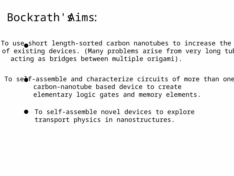
Bockrath's Aims:
To self-assemble and characterize circuits of more than onecarbon-nanotube based device to create elementary logic gates and memory elements.
To use short length-sorted carbon nanotubes to increase the yieldof existing devices. (Many problems arise from very long tubesacting as bridges between multiple origami).
To self-assemble novel devices to explore transport physics in nanostructures.

Rationally Engineered Logic gates and Memory Elements Utilizing Multiple Nanotubes
Vs
Vin
Vout
Vs
Vout
Vs
Vs
Vin1
Vout
Vin2
Inverter
SRAM
NOR
Nanotube assembly Schematic circuit diagram

B
V
I
Novel Devices Probing Transport Physics in Nanostructures: Phase Coherence in Strongly-Interacting Electron Systems
Nanotubes act as a “which path?” interferometer enabling the study of phase coherent transport in Nanotube-based Luttinger liquids via a transport experiment. The setup is analogous to a double slit experiment in optics. The magnetic field B tunes the phase by the Ahoronov-Bohm effect. Tubes must be closer together than the phase coherence length in the electrodes, which is readily obtainable using DNA based self-assembly.
Tunable separation with desired values ~5-20 nm
DNA origami template for parallel nanotubes
Interferometer device
source drain
Many possibilities exist for making novel devices.

Goddard's Aims:Electron transport in DNA-carbon nanotube hybrids:The effect of an insulating DNA layer between carbon nanotubes,silicon nanowires, and quantum dots is unknown. In some casesDNA may be removed from devices post-assembly, in other casesmay remain. Thus it is important to simulate electron transport incarbon nanotube devices, with and without intervening DNA, startingwith atomistic simulation (Next slide).
Simulations of the placement process:The interactions which bind DNA structures to technologicalsurfaces like silicon or diamond-like carbon are poorly understood.The best choice of experimental conditions, as well as the bestchoice of DNA shapes to bind can be explored by atomistic andmesoscale simulation. Free energies of correct and mismatchedbinding, and possible kinetic traps can be explored.
patterned DLC on Si possible kinetic traps and mismatches

• Size of molecules << scattering lengths (e.g. mean free path, de Broglie wavelength, etc.) -> quantum descriptions necessary.
• Quantum chemistry of molecule(s) + nanotube -> charge flow & bonding -> geometry & energy spectrum of the entire system.
• Organo-metallic interface mechanics and transport. Need to treat molecule as finite and nanotubes as semi-infinite electrodes.
• Escape currents (through organic insulator layer).• Conformation effects on electronic transport.• Effect of finite bias.
• IV characteristic of self-assembled CNT-based transistor junctions.
HOMO
LUMO FE
V
2μ
1μ
ICNT
DNA
Organic molecule
CNT
V
DNA-origami CNT-based Transistor Junctions
Theory and Modeling to Describe…

Multiscale Methodology:1st-principles I-V validated by
rotaxane modeling
Density-functional theory (Hohenberg-Kohn-Sham)Density-functional theory (Hohenberg-Kohn-Sham)
Ballistic transport theory (Landauer, Buttiker)Ballistic transport theory (Landauer, Buttiker)
T(E,V)
contact widening
self-energy
Green’s ftn. Formalism (Fisher-Lee)Green’s ftn. Formalism (Fisher-Lee)
transmission
electro-chemical potential
conductance
current
HneV ⇒=− , 11 μμ
I =2eh
T(E,V) f1(E −μ2 )− f2 (E −μ1)[ ]dE −∞
∞
∫
G =dIdV
≈2e2
hT
Gm =(EmSm −Hm −Σ1 −Σ2 )−1
Γ1,2 =i Σ1,2 −Σ1,2+( )
T (E,V ) =Tr Γ1GΓ2G+( )
F =m
d2Rdt2
Molecular Mechanics
Dynamics
Molecular Mechanics
Dynamics
geometry
OSS
SS OO O
OO
O
O
O
N N
N N
OSO
S +
+ +
+
4PF6–
O O O
O
O
S S
O O OS
S
S
SO O O
O
O
SS
N
N
N
N
+
++
+
4 P F6–
5
4
3
2
1
0
0 .1 00 .0 50 .0 0-0 .0 5-0 .1 0
-3
-2
-1
0
1
2
3
6 04 02 00-2 0-4 0-6 0
Mono -disulfide [2]Rotaxane Bis -disulfide [2]Rotaxane
- 3- 2
- 10
1
4 00- 4 0x 1 0
- 3
@ gate volta ge 2.55V
2 0 0
1 0 0
0
- 1 0 0
- 2 0 0
1 0 05 00- 5 0- 1 0 0x1 0
- 3
@ gate volta ge 2.4V
Lower curre nt, asymmetric I-V Hig her current, symmetric I-V
dI/dV vs . junction bias and gate bias
source to drain volta ge (mV)source to drain volta ge (mV)
symmetric dI/dV plo t vs junction bias
OSS
SS OO O
OO
O
O
O
N N
N N
OSO
S +
+ +
+
4PF6–
OSS
SS OO O
OO
O
O
O
N N
N N
OSO
S +
+ +
+
4PF6–4PF6–
O O O
O
O
S S
O O OS
S
S
SO O O
O
O
SS
N
N
N
N
+
++
+
4 P F6–
5
4
3
2
1
0
0 .1 00 .0 50 .0 0-0 .0 5-0 .1 0
-3
-2
-1
0
1
2
3
6 04 02 00-2 0-4 0-6 0
Mono -disulfide [2]Rotaxane Bis -disulfide [2]Rotaxane
- 3- 2
- 10
1
4 00- 4 0x 1 0
- 3
@ gate volta ge 2.55V
2 0 0
1 0 0
0
- 1 0 0
- 2 0 0
1 0 05 00- 5 0- 1 0 0x1 0
- 3
@ gate volta ge 2.4V
Lower curre nt, asymmetric I-V Hig her current, symmetric I-V
dI/dV vs . junction bias and gate bias
source to drain volta ge (mV)source to drain volta ge (mV)
symmetric dI/dV plo t vs junction bias
dI/dVe.g. Rotaxane switch
Γ1 Γ2
1m
2

Further validation: bi-phenyl-dithiol modeling
Au (111)
∫ −= 2
1
))(,(2
)( 21
μ
μdEffVET
h
eVI
T(E)
I(V)molecule
contact
contact

Relevance to the Office of Naval Research
DNA self-assembly uses non-hazardous "green" chemistries,decreasing the Navy's environmental footprint.
Fundamental advances in microelectronics underlie all ofour country's defense systems, from networked warfare toavionic systems. Eventually, self-assembly based methods maybe the only path forward to more powerful nanoelectronic systems.
DNA self-assembly techniques may yield lower costelectronics "grown" from cheap components withoutcapital investment in conventional chip fabs.

Budget for 4 years, $2.6 million including:
PI: Paul Rothemund: $200K/yr for Senior Research Associate salary and materials
Co-PI: Mark Bockrath $100K/yr for 1 graduate student and materials
Co-PI: Bill Goddard $100K/yr for 1 graduate student and materials
Co-PI: Erik Winfree $100K/yr for 1 graduate student and materials
Equipment $150K/yr including plasma etcher/cleaner ($20K), wafer-scale Atomic Force Microscope ($200K) temperature-controlled dynamic light scattering ($50K).


![The Caltech DNA- nanoelectronics teamdna.caltech.edu/~pwkr/talks/ONR-DNA-nanoelectronics.pdf · The Caltech DNA-nanoelectronics team PI Paul Rothemund, ... D [n A] V g [V] I S D S](https://img.pdfslide.us/doc/110x75/5a962fc57f8b9ad96f8cc74c/the-caltech-dna-nanoelectronics-pwkrtalksonr-dna-nanoelectronicspdfthe-caltech.jpg)