Embed Size (px)
Citation preview
Solid State Device Fundamentals
ENS 345
Lecture Course
by
Alexander M. Zaitsev
Tel: 718 982 2812
Office 4N101b
College of Staten Island / CUNY Department of Engineering Science and Physics
1
2. Crystals
College of Staten Island / CUNY Department of Engineering Science and Physics
Solid State Device Fundamentals
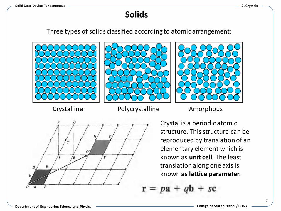
Solids
Crystal is a periodic atomic structure. This structure can be reproduced by translation of an elementary element which is known as unit cell. The least translation along one axis is known as lattice parameter.
2
Three types of solids classified according to atomic arrangement:
Crystalline Polycrystalline Amorphous
2. Crystals
Department of Engineering Science and Physics
Solid State Device Fundamentals
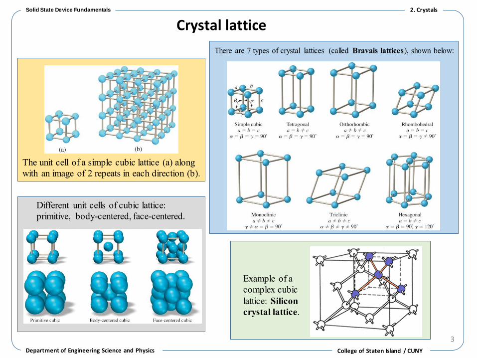
Crystal lattice
The unit cell of a simple cubic lattice (a) along
with an image of 2 repeats in each direction (b).
Example of a
complex cubic
lattice: Silicon
crystal lattice.
3
College of Staten Island / CUNY
Different unit cells of cubic lattice:
primitive, body-centered, face-centered.
There are 7 types of crystal lattices (called Bravais lattices), shown below:
2. Crystals
College of Staten Island / CUNY Department of Engineering Science and Physics
Solid State Device Fundamentals
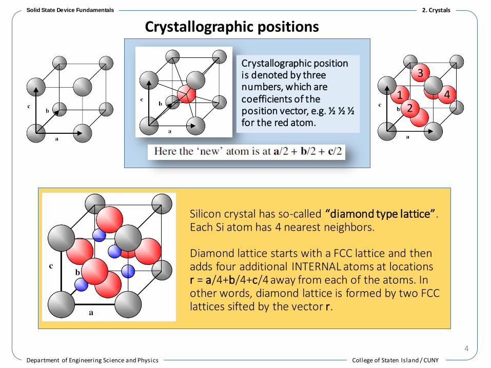
Crystallographic positions
4
Silicon crystal has so-called “diamond type lattice”.Each Si atom has 4 nearest neighbors.
Diamond lattice starts with a FCC lattice and then adds four additional INTERNAL atoms at locationsr = a/4+b/4+c/4 away from each of the atoms. In other words, diamond lattice is formed by two FCC lattices sifted by the vector r.
Crystallographic position is denoted by three numbers, which are coefficients of the position vector, e.g. ½ ½ ½ for the red atom.
2. Crystals
12
3
4
College of Staten Island / CUNY Department of Engineering Science and Physics
Solid State Device Fundamentals
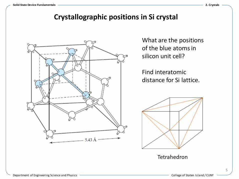
Crystallographic positions in Si crystal
5
What are the positions of the blue atoms in silicon unit cell?
Find interatomic distance for Si lattice.
Tetrahedron
2. Crystals
6College of Staten Island / CUNY Department of Engineering Science and Physics
Solid State Device Fundamentals
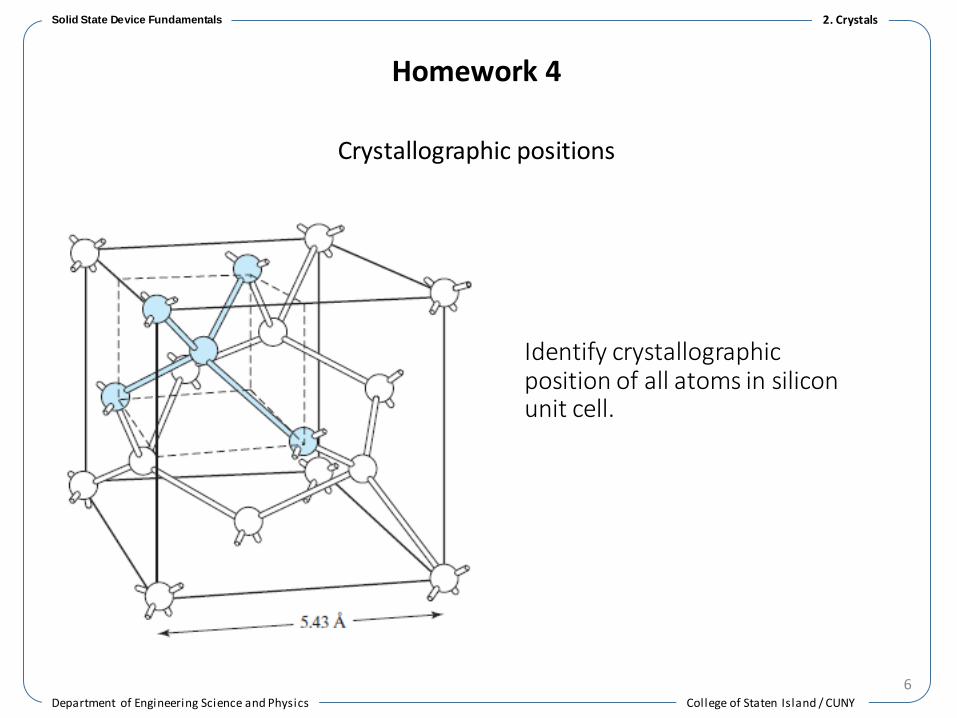
Homework 4
Crystallographic positions
Identify crystallographic position of all atoms in silicon unit cell.
2. Crystals
College of Staten Island / CUNY Department of Engineering Science and Physics
Solid State Device Fundamentals
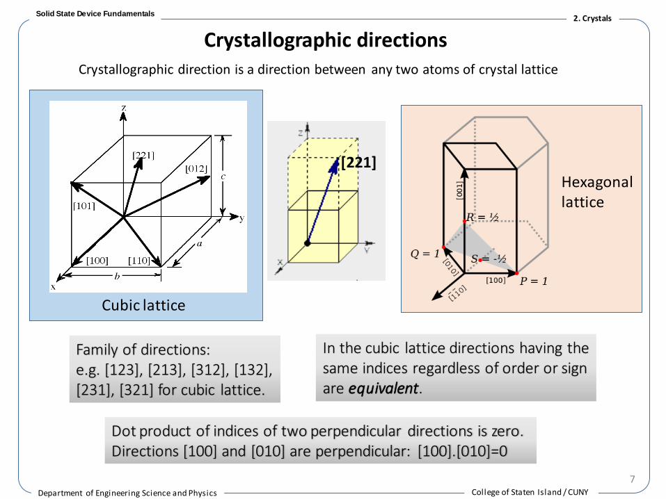
Crystallographic directions
7
Crystallographic direction is a direction between any two atoms of crystal lattice
[221]
Cubic lattice
Hexagonallattice
2. Crystals
Family of directions:e.g. [123], [213], [312], [132], [231], [321] for cubic lattice.
In the cubic lattice directions having the same indices regardless of order or sign are equivalent.
Dot product of indices of two perpendicular directions is zero. Directions [100] and [010] are perpendicular: [100].[010]=0
College of Staten Island / CUNY Department of Engineering Science and Physics
Solid State Device Fundamentals
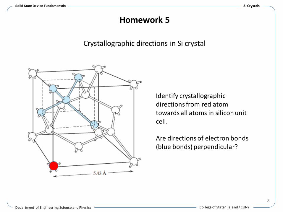
Homework 5
Crystallographic directions in Si crystal
8
Identify crystallographic directions from red atom towards all atoms in silicon unit cell.
Are directions of electron bonds (blue bonds) perpendicular?
2. Crystals
9College of Staten Island / CUNY Department of Engineering Science and Physics
Solid State Device Fundamentals
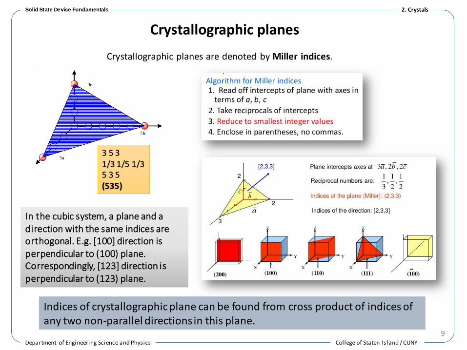
Crystallographic planes
Crystallographic planes are denoted by Miller indices.
3 5 31/3 1/5 1/35 3 5(535)
2. Crystals
In the cubic system, a plane and a direction with the same indices are orthogonal. E.g. [100] direction is perpendicular to (100) plane. Correspondingly, [123] direction is perpendicular to (123) plane.
Indices of crystallographic plane can be found from cross product of indices of any two non-parallel directions in this plane.
10College of Staten Island / CUNY Department of Engineering Science and Physics
Solid State Device Fundamentals
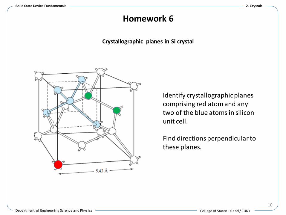
Homework 6
Crystallographic planes in Si crystal
Identify crystallographic planes comprising red atom and any two of the blue atoms in silicon unit cell.
Find directions perpendicular to these planes.
2. Crystals
11College of Staten Island / CUNY Department of Engineering Science and Physics
Solid State Device Fundamentals
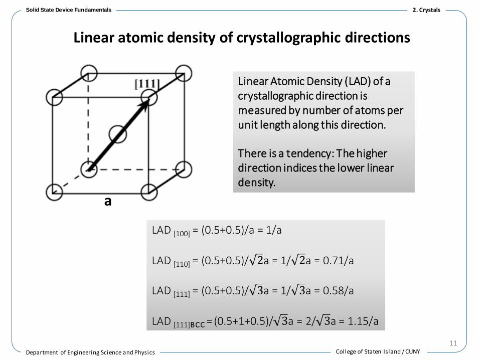
Linear atomic density of crystallographic directions
Linear Atomic Density (LAD) of a crystallographic direction is measured by number of atoms per unit length along this direction.
There is a tendency: The higher direction indices the lower linear density.
a
LAD [100] = (0.5+0.5)/a = 1/a
LAD [110] = (0.5+0.5)/ 2a = 1/ 2a = 0.71/a
LAD [111] = (0.5+0.5)/ 3a = 1/ 3a = 0.58/a
LAD [111]BCC = (0.5+1+0.5)/ 3a = 2/ 3a = 1.15/a
2. Crystals
12College of Staten Island / CUNY Department of Engineering Science and Physics
Solid State Device Fundamentals
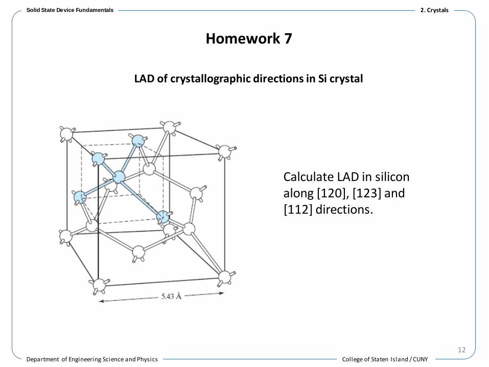
Calculate LAD in silicon along [120], [123] and [112] directions.
Homework 7
LAD of crystallographic directions in Si crystal
2. Crystals
13College of Staten Island / CUNY Department of Engineering Science and Physics
Solid State Device Fundamentals
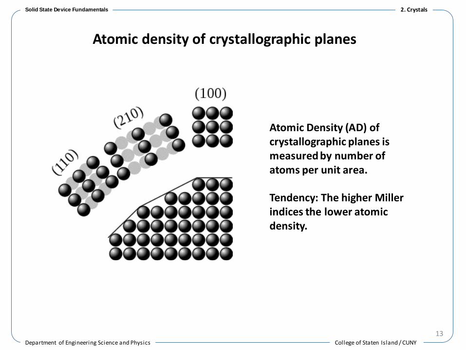
Atomic density of crystallographic planes
Atomic Density (AD) of crystallographic planes is measured by number of atoms per unit area.
Tendency: The higher Miller indices the lower atomic density.
2. Crystals
14College of Staten Island / CUNY Department of Engineering Science and Physics
Solid State Device Fundamentals
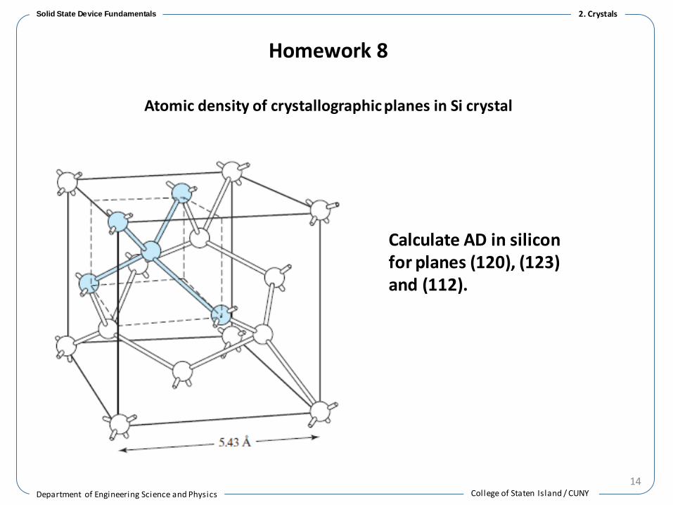
Calculate AD in silicon for planes (120), (123) and (112).
Homework 8
Atomic density of crystallographic planes in Si crystal
2. Crystals
College of Staten Island / CUNY Department of Engineering Science and Physics
Solid State Device Fundamentals
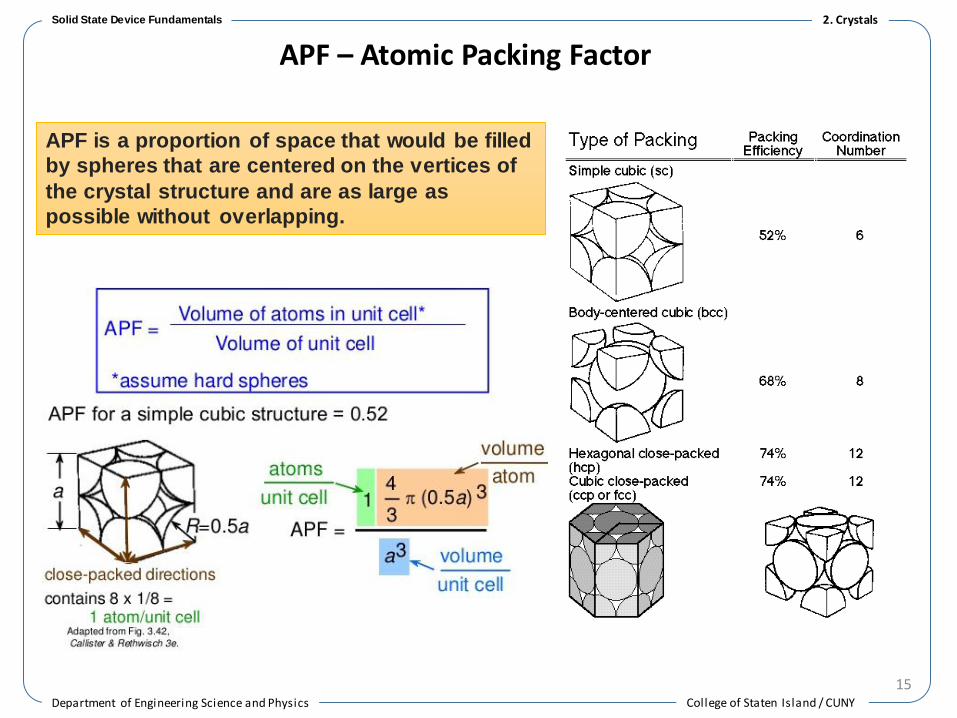
APF – Atomic Packing Factor
15
APF is a proportion of space that would be filled
by spheres that are centered on the vertices of
the crystal structure and are as large as
possible without overlapping.
2. Crystals
16College of Staten Island / CUNY Department of Engineering Science and Physics
Solid State Device Fundamentals
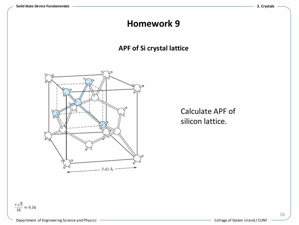
Calculate APF of silicon lattice.
Homework 9
APF of Si crystal lattice
2. Crystals
College of Staten Island / CUNY Department of Engineering Science and Physics
Solid State Device Fundamentals
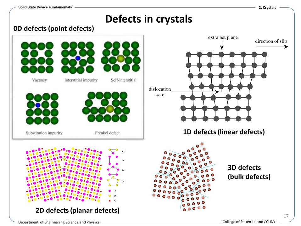
Defects in crystals
17
0D defects (point defects)
1D defects (linear defects)
2D defects (planar defects)
3D defects(bulk defects)
2. Crystals