Embed Size (px)
Citation preview
Invited paper SOI Technology:
An Opportunity for RF Designers?Jean-Pierre Raskin
Abstract— This last decade silicon-on-insulator (SOI) MOS-
FET technology has demonstrated its potentialities for high
frequency (reaching cutoff frequencies close to 500 GHz for
n-MOSFETs) and for harsh environments (high temperature,
radiation) commercial applications. For RF and system-on-
chip applications, SOI also presents the major advantage of
providing high resistivity substrate capabilities, leading to sub-
stantially reduced substrate losses. Substrate resistivity values
higher than 1 kΩΩΩ cm can easily be achieved and high resistivity
silicon (HRS) is commonly foreseen as a promising substrate
for radio frequency integrated circuits (RFIC) and mixed sig-
nal applications. In this paper, based on several experimental
and simulation results the interest, limitations but also pos-
sible future improvements of the SOI MOS technology are
presented.
Keywords— crosstalk, high resistivity silicon substrate, MOS-
FET, nonlinearities, silicon-on-insulator, wideband characteri-
zation.
1. Introduction
The semiconductor technology has been progressing enor-
mously these last decades, such evolution has been driven
by the continuous look for the increase of the operation
speed and the integration density of complex digital cir-
cuits [1]. In the early 70’s a scaling-down procedure of
the transistor dimensions established by Dennard and co-
workers [2] was proposed to pave the way to reaching both
objectives. From those days to now, the keystone of the
semiconductor industry has been the optimization of this
scaling-down procedure.
The communication industry has always been a very chal-
lenging and profitable market for the semiconductor com-
panies. The new communication systems are today very de-
manding; high frequency, high degree of integration, multi-
standards, low power consumption, and they have to present
good performance even under harsh environment such as
high temperature, radiation, etc. The integration and power
consumption reduction of the digital part will further im-
prove with the continued downscaling of technologies. The
bottleneck for further advancement is the analog front-end.
Present-day transceivers often consist of three or four chip-
set solutions combined with several external components.
A reduction of the external components is essential to ob-
tain lower cost, power consumption and weight, but it will
lead to a fundamental change in the design of analog front-
end architectures. The analog front-end requires a high
performance technology, like GaAs or silicon bipolar, with
devices that can easily achieve operating frequencies in
the GHz range. For the digital signal processor a small
device feature size is essential for the implementation of
complex algorithms. Therefore, it appears that only the
best submicron CMOS technologies could provide a fea-
sible and cost-effective integration of the communication
systems.
This last decade metal oxide semiconductor (MOS) tran-
sistors have reached amazingly high operation speed and
the semiconductor community has started to notice the ra-
dio frequency (RF) possibilities of such mainstream de-
vices. Silicon-on-insulator (SOI) MOSFET technology has
demonstrated its potentialities for high frequency (reaching
cutoff frequencies close to 500 GHz for n-MOSFETs [3])
and for harsh environments (high temperature, radiations)
commercial applications.
From its early development phase till recent years, SOI has
grown from a mere scientific curiosity into a mature tech-
nology. Partially depleted (PD) SOI is now massively serv-
ing the 45-nm digital market where it is seen as a low cost –
low power alternative to bulk silicon. Fully depleted (FD)
devices are also widely spread as they outperform exist-
ing semiconductor technologies for extremely low power
analog applications [4].
For RF and system-on-chip applications, SOI also presents
the major advantage of providing high resistivity sub-
strate capabilities, leading to substantially reduced substrate
losses. Substrate resistivity values higher than 1 kΩcm can
easily be achieved and high resistivity silicon (HRS) is
commonly foreseen as a promising substrate for radio fre-
quency integrated circuits (RFIC) and mixed signal appli-
cations [5].
In this paper, based on several experimental and simula-
tion results the interest, limitations but also possible fu-
ture improvements of the SOI MOSFET technology for mi-
crowaves and millimeter-waves applications are presented.
2. State of the Art RF Performance
Since the invention of the bipolar transistor in 1947, the
operating frequencies of integrated transistors have been
improved every year. In 1958, a cut-off frequency above
1 GHz is reached with a germanium bipolar transistor [6].
Since that date, several integrated technologies have been
investigated and improved to further increase the operating
frequency of transistors. In 1965, a GaAs metal semicon-
ductor field effect transistor (MESFET) appears in the liter-
ature [7]. In 1973, a maximum oscillation frequency ( fmax)
of 100 GHz is measured for a FET [8]. In 1980, a new
architecture of field effect transistor with high electron mo-
3
Jean-Pierre Raskin
bility (HEMT) is proposed and fabricated [9]. In 1995,
a cutoff frequency fmax higher than 500 GHz is extrapolated
for a HEMT [10]. In 2000, the limit of 1 THz is reached
with III-V heterostructure bipolar transistor (HBT) [11] and
even overpassed by HEMT in 2007 [12].
It is only in 1996, thanks to the successful downscaling
of the silicon MOSFET gate, that cutoff frequencies higher
than 200 GHz are presented [13]. Since that date, the inter-
est in MOSFETs for low voltage, low power, high integra-
tion mixed-mode ICs (digital and analog parts on the same
chip) in the field of microwaves and millimeter-waves ap-
plications has been constantly growing. MOSFET is a well-
known, well-controlled and mature technology, as well as
cost effective, which makes it the key technology for mass
production.
Nowadays, thanks to the introduction of mobility booster
such as strained silicon channel, cutoff frequencies
close to 500 GHz and 350 GHz are achieved, respec-
tively, for n- and p-MOSFETs [3] with the channel length
of 30 nm.
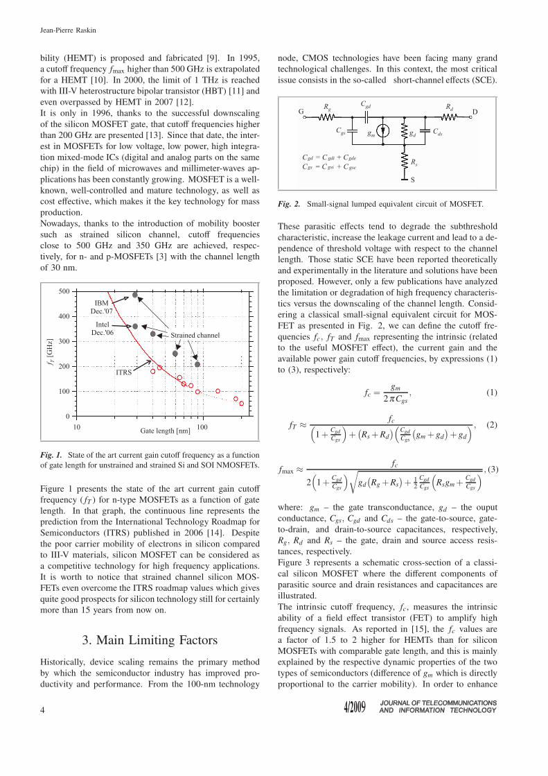
Fig. 1. State of the art current gain cutoff frequency as a function
of gate length for unstrained and strained Si and SOI NMOSFETs.
Figure 1 presents the state of the art current gain cutoff
frequency ( fT ) for n-type MOSFETs as a function of gate
length. In that graph, the continuous line represents the
prediction from the International Technology Roadmap for
Semiconductors (ITRS) published in 2006 [14]. Despite
the poor carrier mobility of electrons in silicon compared
to III-V materials, silicon MOSFET can be considered as
a competitive technology for high frequency applications.
It is worth to notice that strained channel silicon MOS-
FETs even overcome the ITRS roadmap values which gives
quite good prospects for silicon technology still for certainly
more than 15 years from now on.
3. Main Limiting Factors
Historically, device scaling remains the primary method
by which the semiconductor industry has improved pro-
ductivity and performance. From the 100-nm technology
node, CMOS technologies have been facing many grand
technological challenges. In this context, the most critical
issue consists in the so-called short-channel effects (SCE).
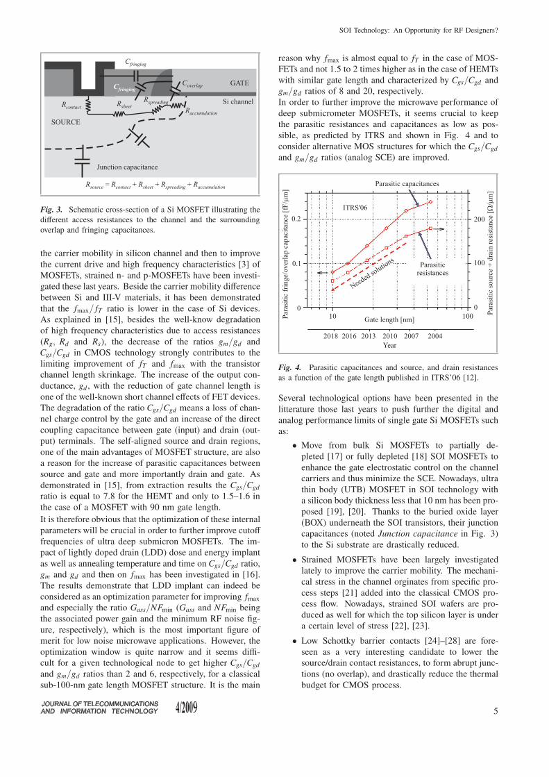
Fig. 2. Small-signal lumped equivalent circuit of MOSFET.
These parasitic effects tend to degrade the subthreshold
characteristic, increase the leakage current and lead to a de-
pendence of threshold voltage with respect to the channel
length. Those static SCE have been reported theoretically
and experimentally in the literature and solutions have been
proposed. However, only a few publications have analyzed
the limitation or degradation of high frequency characteris-
tics versus the downscaling of the channel length. Consid-
ering a classical small-signal equivalent circuit for MOS-
FET as presented in Fig. 2, we can define the cutoff fre-
quencies fc, fT and fmax representing the intrinsic (related
to the useful MOSFET effect), the current gain and the
available power gain cutoff frequencies, by expressions (1)
to (3), respectively:
fc =gm
2π Cgs
, (1)
fT ≈fc
(
1 +Cgd
Cgs
)
+(
Rs + Rd
)
(
Cgd
Cgs
(
gm + gd
)
+ gd
) , (2)
fmax ≈fc
2
(
1 +Cgd
Cgs
)
√
gd
(
Rg + Rs
)
+ 1
2
Cgd
Cgs
(
Rsgm +Cgd
Cgs
)
, (3)
where: gm – the gate transconductance, gd – the ouput
conductance, Cgs, Cgd and Cds – the gate-to-source, gate-
to-drain, and drain-to-source capacitances, respectively,
Rg, Rd and Rs – the gate, drain and source access resis-
tances, respectively.
Figure 3 represents a schematic cross-section of a classi-
cal silicon MOSFET where the different components of
parasitic source and drain resistances and capacitances are
illustrated.
The intrinsic cutoff frequency, fc, measures the intrinsic
ability of a field effect transistor (FET) to amplify high
frequency signals. As reported in [15], the fc values are
a factor of 1.5 to 2 higher for HEMTs than for silicon
MOSFETs with comparable gate length, and this is mainly
explained by the respective dynamic properties of the two
types of semiconductors (difference of gm which is directly
proportional to the carrier mobility). In order to enhance
4
SOI Technology: An Opportunity for RF Designers?
Fig. 3. Schematic cross-section of a Si MOSFET illustrating the
different access resistances to the channel and the surrounding
overlap and fringing capacitances.
the carrier mobility in silicon channel and then to improve
the current drive and high frequency characteristics [3] of
MOSFETs, strained n- and p-MOSFETs have been investi-
gated these last years. Beside the carrier mobility difference
between Si and III-V materials, it has been demonstrated
that the fmax/ fT ratio is lower in the case of Si devices.
As explained in [15], besides the well-know degradation
of high frequency characteristics due to access resistances
(Rg, Rd and Rs), the decrease of the ratios gm/gd and
Cgs/Cgd in CMOS technology strongly contributes to the
limiting improvement of fT and fmax with the transistor
channel length skrinkage. The increase of the output con-
ductance, gd , with the reduction of gate channel length is
one of the well-known short channel effects of FET devices.
The degradation of the ratio Cgs/Cgd means a loss of chan-
nel charge control by the gate and an increase of the direct
coupling capacitance between gate (input) and drain (out-
put) terminals. The self-aligned source and drain regions,
one of the main advantages of MOSFET structure, are also
a reason for the increase of parasitic capacitances between
source and gate and more importantly drain and gate. As
demonstrated in [15], from extraction results the Cgs/Cgd
ratio is equal to 7.8 for the HEMT and only to 1.5–1.6 in
the case of a MOSFET with 90 nm gate length.
It is therefore obvious that the optimization of these internal
parameters will be crucial in order to further improve cutoff
frequencies of ultra deep submicron MOSFETs. The im-
pact of lightly doped drain (LDD) dose and energy implant
as well as annealing temperature and time on Cgs/Cgd ratio,
gm and gd and then on fmax has been investigated in [16].
The results demonstrate that LDD implant can indeed be
considered as an optimization parameter for improving fmax
and especially the ratio Gass/NFmin (Gass and NFmin being
the associated power gain and the minimum RF noise fig-
ure, respectively), which is the most important figure of
merit for low noise microwave applications. However, the
optimization window is quite narrow and it seems diffi-
cult for a given technological node to get higher Cgs/Cgd
and gm/gd ratios than 2 and 6, respectively, for a classical
sub-100-nm gate length MOSFET structure. It is the main
reason why fmax is almost equal to fT in the case of MOS-
FETs and not 1.5 to 2 times higher as in the case of HEMTs
with similar gate length and characterized by Cgs/Cgd and
gm/gd ratios of 8 and 20, respectively.
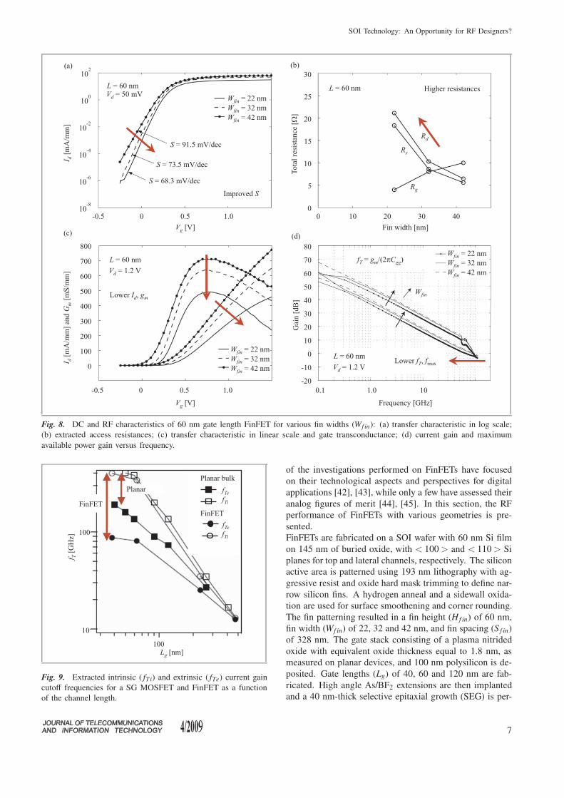
In order to further improve the microwave performance of
deep submicrometer MOSFETs, it seems crucial to keep
the parasitic resistances and capacitances as low as pos-
sible, as predicted by ITRS and shown in Fig. 4 and to
consider alternative MOS structures for which the Cgs/Cgd
and gm/gd ratios (analog SCE) are improved.
Fig. 4. Parasitic capacitances and source, and drain resistances
as a function of the gate length published in ITRS’06 [12].
Several technological options have been presented in the
litterature those last years to push further the digital and
analog performance limits of single gate Si MOSFETs such
as:
• Move from bulk Si MOSFETs to partially de-
pleted [17] or fully depleted [18] SOI MOSFETs to
enhance the gate electrostatic control on the channel
carriers and thus minimize the SCE. Nowadays, ultra
thin body (UTB) MOSFET in SOI technology with
a silicon body thickness less that 10 nm has been pro-
posed [19], [20]. Thanks to the buried oxide layer
(BOX) underneath the SOI transistors, their junction
capacitances (noted Junction capacitance in Fig. 3)
to the Si substrate are drastically reduced.
• Strained MOSFETs have been largely investigated
lately to improve the carrier mobility. The mechani-
cal stress in the channel orginates from specific pro-
cess steps [21] added into the classical CMOS pro-
cess flow. Nowadays, strained SOI wafers are pro-
duced as well for which the top silicon layer is under
a certain level of stress [22], [23].
• Low Schottky barrier contacts [24]–[28] are fore-
seen as a very interesting candidate to lower the
source/drain contact resistances, to form abrupt junc-
tions (no overlap), and drastically reduce the thermal
budget for CMOS process.
5
Jean-Pierre Raskin
• Metal gate allows to get rid of loss of electrostatic
gate control related to the polysilicon gate depletion
[29], [30], as well as to reduce the gate sheet resis-
tance.
• Low-k and air gap [31], [32] should be introduced to
reduce fringing capacitances between gate-to-source
and gate-to-drain electrodes.
• SOI wafers with thin BOX have been proposed these
last years to reduce SCE (for instance, DIBL) but also
to lower self-heating issues [19], [20], [33], [34].
• High resistivity silicon substrate has demonstrated su-
perior characteristics for the integration of high qual-
ity passive elements such as transmission lines [35],
inductors [36], etc., as well as for reduction of the
crosstalk between circuit blocks integrated on the
same silicon chip [5].
This last point will be developed in detail in Section 5.
Figure 5 schematically presents the cross-section of what
we can call an ultimate single gate MOSFET basically in-
cluding the technological options listed above. Unstrained
p-type MOSFET including a metal gate and low Schottky
barrier source and drain contacts has been built and char-
Fig. 5. Schematic cross-section view of an optimized single fully
depleted SOI MOSFET.
Fig. 6. Current gain as a function of frequency for a 30 nm
p-type segregated PtSi Schottky barrier MOSFET.
acterized over a wide frequency band in [27]. The device
architecture features a 20 nm thick SOI channel, a 2.4 nm
SiO2 gate oxide, a metallic tungsten gate and 15 nm-wide
SiN spacers. The integration of a low Schottky barrier
silicide (PtSi) coupled to boron segregation demonstrates
a 50% improvement on the current drive accompanied by
reinforced immunity against SCE when compared to the
dopant-free approach. This constitutes the first implemen-
tation of a dopant segregated band-edge silicide obtained by
implant-to-silicide (ITS) and activated at low temperature
(500°C). The RF characterization unveils a unity current
gain cut-off frequency fT of 180 GHz for a 30 nm gate
long device as shown in Fig. 6. This constitutes the best
result reported in literature [37] for unstrained channel fully
depleted SOI p-MOSFETs.
Multiple gate MOSFETs are often cited as the ultimate
MOS devices to reduce the SCE. The analog and RF per-
formances of FinFETs are presented in the following sec-
tion.
4. RF Performance of a Multigate
MOSFET: FinFET
To reduce the SCE in nanometer scale MOSFETs, multiple-
gate architectures emerge as one of the most promis-
ing novel device structures, thanks to the simultaneous
control of the channel by more than one gate. The
idea of the double-gate (DG) MOSFET was first intro-
duced by J.-P. Colinge [38]. Starting by the FinFET [39],
other multiple-gate SOI MOSFETs have been introduced
since [40] such as triple-gate (TG), FinFET, pi-gate (PG),
quadruple-gate (QG), omega-gate (Ω-G), etc. Many works
have investigated and demonstrated the great potential of
multiple-gate devices to comply with the Ion/Io f f require-
ments of the ITRS for logic operation [40], [41].
Fig. 7. Schematic top view of a FinFET composed of 10 fins (up-
per) and SG MOSFET (lower) occupying the same active silicon
foot print.
Indeed, FinFETs are known to be promising devices for
high density digital applications in the sub-65 nm nodes
due to their high immunity to short channel effects and their
excellent compatibility with planar CMOS process. Most
6
SOI Technology: An Opportunity for RF Designers?
Fig. 8. DC and RF characteristics of 60 nm gate length FinFET for various fin widths (Wf in): (a) transfer characteristic in log scale;
(b) extracted access resistances; (c) transfer characteristic in linear scale and gate transconductance; (d) current gain and maximum
available power gain versus frequency.
Fig. 9. Extracted intrinsic ( fTi) and extrinsic ( fTe) current gain
cutoff frequencies for a SG MOSFET and FinFET as a function
of the channel length.
of the investigations performed on FinFETs have focused
on their technological aspects and perspectives for digital
applications [42], [43], while only a few have assessed their
analog figures of merit [44], [45]. In this section, the RF
performance of FinFETs with various geometries is pre-
sented.
FinFETs are fabricated on a SOI wafer with 60 nm Si film
on 145 nm of buried oxide, with < 100 > and < 110 > Si
planes for top and lateral channels, respectively. The silicon
active area is patterned using 193 nm lithography with ag-
gressive resist and oxide hard mask trimming to define nar-
row silicon fins. A hydrogen anneal and a sidewall oxida-
tion are used for surface smoothening and corner rounding.
The fin patterning resulted in a fin height (H f in) of 60 nm,
fin width (Wf in) of 22, 32 and 42 nm, and fin spacing (S f in)
of 328 nm. The gate stack consisting of a plasma nitrided
oxide with equivalent oxide thickness equal to 1.8 nm, as
measured on planar devices, and 100 nm polysilicon is de-
posited. Gate lengths (Lg) of 40, 60 and 120 nm are fab-
ricated. High angle As/BF2 extensions are then implanted
and a 40 nm-thick selective epitaxial growth (SEG) is per-
7
Jean-Pierre Raskin
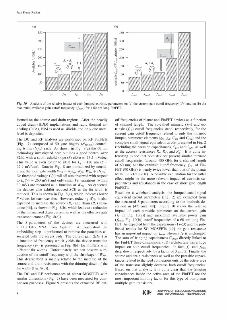
Fig. 10. Analysis of the relative impact of each lumped extrinsic parameters on (a) the current gain cutoff frequency ( fT ) and on (b) the
maximum available gain cutoff frequency ( fmax) for a 60 nm long FinFET.
formed on the source and drain regions. After the heavily
doped drain (HDD) implantations and rapid thermal an-
nealing (RTA), NiSi is used as silicide and only one metal
level is deposited.
The DC and RF analyses are performed on RF FinFETs
(Fig. 7) composed of 50 gate fingers (N f inger) control-
ing 6 fins (N f in) each. As shown in Fig. 8(a) the 60 nm
technology investigated here outlines a good control over
SCE, with a subthreshold slope (S) close to 73.5 mV/dec.
This value is even closer to ideal for Lg = 120 nm (S =62.9 mV/dec). Data in Fig. 8 are normalized by consid-
ering the total gate width Wtot = N f ingerN f in(Wf in +2H f in).No threshold voltage (VT ) roll off was observed with respect
to Lg(VT ∼ 260 mV) and only small VT variations (within
30 mV) are recorded as a function of Wf in. As expected,
the devices also exhibit reduced SCE as the fin width is
reduced. This is shown in Fig. 8(a), which indicates lower
S values for narrower fins. However, reducing Wf in is also
expected to increase the source (Rs) and drain (Rd) resis-
tance [46], as shown in Fig. 8(b), which leads to a reduction
of the normalized drain current as well as the effective gate
transconductance (Fig. 8(c)).
The S-parameters of the devices are measured with
a 110 GHz VNA from Agilent. An open-short de-
embedding step is performed to remove the parasitics as-
sociated with the access pads. The current gain (|H21|) as
a function of frequency which yields the device transition
frequency ( fT ) is presented in Fig. 8(d) for FinFETs with
different fin widths. Unfortunately, we can observe a re-
duction of the cutoff frequency with the shrinkage of Wf in.
This degradation is mainly related to the increase of the
source and drain resistances with the thinning down of the
fin width (Fig. 8(b)).
The DC and RF performances of planar MOSFETs with
similar dimensions (Fig. 7) have been measured for com-
parison purposes. Figure 9 presents the extracted RF cut-
off frequencies of planar and FinFET devices as a function
of channel length. The so-called intrinsic ( fTi) and ex-
trinsic ( fTe) cutoff frequencies stand, respectively, for the
current gain cutoff frequency related to only the intrinsic
lumped parameter elements (gm, gd , Cgsi and Cgdi) and the
complete small-signal equivalent circuit presented in Fig. 2
(including the parasitic capacitances, Cgse and Cgde, as well
as the accesss resistances Rs, Rd , and Rg). It is quite in-
teresting to see that both devices present similar intrinsic
cutoff frequencies (around 400 GHz for a channel length
of 60 nm) but the extrinsic cutoff frequency, fTe, of Fin-
FET (90 GHz) is nearly twice lower than that of the planar
MOSFET (180 GHz). A possible explanation for the latter
effect might be the more relevant impact of extrinsic ca-
pacitances and resistances in the case of short gate length
FinFETs.
Based on a wideband analysis, the lumped small-signal
equivalent circuit parameters (Fig. 2) are extracted from
the measured S-parameters according to the methods de-
scribed in [47] and [48]. Figure 10 shows the relative
impact of each parasitic parameter on the current gain
( fT in Fig. 10(a)) and maximum available power gain
( fmax, Fig. 10(b)) cutoff frequencies of a 60 nm long Fin-
FET. As expected from the expressions (1)–(3) and the pub-
lished results for SG MOSFETs [49] the gate resistance
has an important impact on fmax whereas fT is unchanged.
The sum of fringing capacitances Cinner directly linked to
the FinFET three-dimensional (3D) architecture has a huge
impact on both cutoff frequencies. In fact, fT and fmax
drop down, respectively, by a factor of 3 and 2. Finally, the
source and drain resistances as well as the parasitic capaci-
tances related to the feed connexions outside the active area
of the transistor slightly decrease both cutoff frequencies.
Based on that analysis, it is quite clear that the fringing
capacitances inside the active area of the FinFET are the
most important limiting factor for this type of non-planar
multiple gate transistors.
8
SOI Technology: An Opportunity for RF Designers?
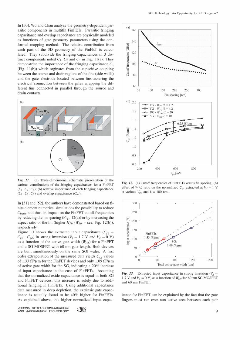
In [50], Wu and Chan analyze the geometry-dependent par-
asitic components in multifin FinFETs. Parasitic fringing
capacitance and overlap capacitance are physically modeled
as functions of gate geometry parameters using the con-
formal mapping method. The relative contribution from
each part of the 3D geometry of the FinFET is calcu-
lated. They subdivide the fringing capacitances in 3 dis-
tinct components noted C1, C2 and C3 in Fig. 11(a). They
demonstrate the importance of the fringing capacitance C3
(Fig. 11(b)) which orginates from the capacitive coupling
between the source and drain regions of the fins (side walls)
and the gate electrode located between fins assuring the
electrical connection between the gates wrapping the dif-
ferent fins connected in parallel through the source and
drain contacts.
Fig. 11. (a) Three-dimensional schematic presentation of the
various contributions of the fringing capacitances for a FinFET
(C1, C2, C3); (b) relative importance of each fringing capacitance
(C1, C2, C3) and overlap capacitance (Cov).
In [51] and [52], the authors have demonstrated based on fi-
nite element numerical simulations the possibility to reduce
Cinner and thus its impact on the FinFET cutoff frequencies
by reducing the fin spacing (Fig. 12(a)) or by increasing the
aspect ratio of the fin (higher H f in/Wf in – see, Fig. 12(b)),
respectively.
Figure 13 shows the extracted input capacitance (Cgg =Cgs +Cgd) in strong inversion (Vg = 1.7 V and Vd = 0 V)
as a function of the active gate width (Wtot) for a FinFET
and a SG MOSFET with 60 nm gate length. Both devices
are built simultanuously on the same SOI wafer. A first
order extrapolation of the measured data yields Cgg values
of 1.33 fF/µm for the FinFET devices and only 1.09 fF/µm
of active gate width for the SG, indicating a 20% increase
of input capacitance in the case of FinFETs. Assuming
that the normalized oxide capacitance is equal in both SG
and FinFET devices, this increase is solely due to addi-
tional fringing in FinFETs. Using additional capacitance
data measured in deep depletion, the extrinsic gate capac-
itance is actually found to be 40% higher for FinFETs.
As explained above, this higher normalized input capac-
Fig. 12. (a) Cutoff frequencies of FinFETs versus fin spacing; (b)
effect of W/L ratio on the normalized Cgs extracted at Vd = 1 V
at various Vgo and L = 100 nm.
Fig. 13. Extracted input capacitance in strong inversion (Vg =1.7 V and Vd = 0 V) as a function of Wtot for 60 nm SG MOSFET
and 60 nm FinFET.
itance for FinFET can be explained by the fact that the gate
fingers must run over non active area between each pair
9
Jean-Pierre Raskin
of parallel fins, a situation that is not encountered in SG
MOSFETs.
To summarize, the simulation and experimental results in-
dicate that FinFET is a multiple gate structure of interest to
reduce digital short channel effects and then assure a lower
threshold voltage roll-off, a better subthreshold slope and
then higher Ion/Io f f ratio, but the high frequency perfor-
mance such as the cutoff frequencies as well as RF noise
figure as presented in [53] are degraded compared to its
SG MOSFET counterpart because of the increased fring-
ing capacitance linked to its complex 3D non-planar ar-
chitecture. Consequently, a trade-off exists regarding Wf in
between high fT and fmax (large Wf in) and good control of
SCE (small Wf in).
5. High Resistivity SOI Substrate
5.1. Coplanar Waveguides Transmission Lines
The use of high resistivity silicon substrate is mandatory
to reduce as much as possible the high frequency losses
associated with the substrate conductivity. High resistivity
silicon substrate cannot be introduced in the case of bulk
Si MOSFETs due to the problem related to latch-up be-
tween devices. In SOI technology, thanks to the buried
oxide the thin top silicon layer in which the transistors are
implemented is electrically isolated from the Si substrate
which can have high resistivity without impacting the good
behavior of the MOS integrated circuits (ICs). Recently,
high quality coplanar waveguides (CPW) presenting inser-
tion loss of less than 2 dB/mm at 200 GHz as well as
low- and high-pass filters at millimeter waves have been
succefully built in an industrial SOI CMOS process envi-
ronment [54].
The insertion loss of a CPW line lying on a lossy silicon
substrate depends on the conductor loss (αcond) and the
substrate loss (αsub) which is inversely proportional to the
effective resistivity of the substrate. The effective resistiv-
ity represents the value of the substrate resistivity that is
actually seen by the coplanar devices. This parameter ac-
counts for the wafer inhomogeneities (i.e., oxide covering
and space charge effects) and corresponds to the resistiv-
ity that a uniform (without oxide nor space charge effects)
silicon wafer should have in order to sustain identical RF
substrate losses. The effective resistivity is extracted from
the measured S-parameters of the CPW line with a method
depicted in [55].
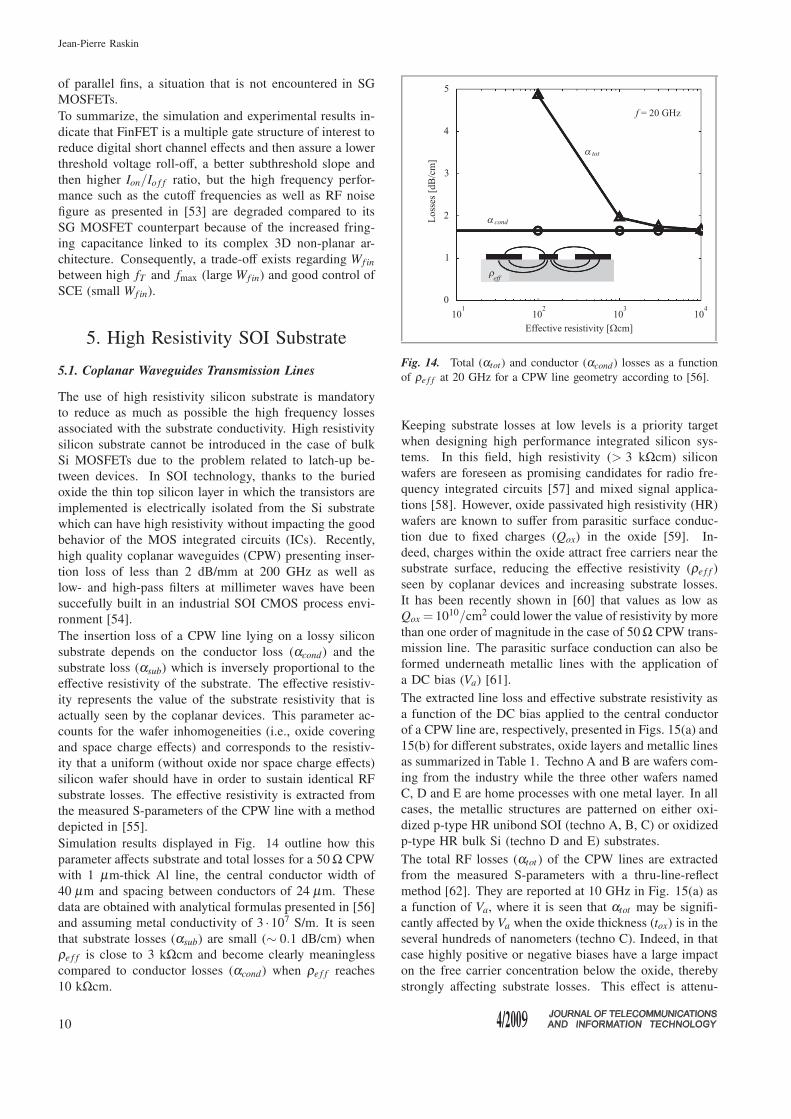
Simulation results displayed in Fig. 14 outline how this
parameter affects substrate and total losses for a 50 Ω CPW
with 1 µm-thick Al line, the central conductor width of
40 µm and spacing between conductors of 24 µm. These
data are obtained with analytical formulas presented in [56]
and assuming metal conductivity of 3 ·107 S/m. It is seen
that substrate losses (αsub) are small (∼ 0.1 dB/cm) when
ρe f f is close to 3 kΩcm and become clearly meaningless
compared to conductor losses (αcond) when ρe f f reaches
10 kΩcm.
Fig. 14. Total (αtot) and conductor (αcond) losses as a function
of ρe f f at 20 GHz for a CPW line geometry according to [56].
Keeping substrate losses at low levels is a priority target
when designing high performance integrated silicon sys-
tems. In this field, high resistivity (> 3 kΩcm) silicon
wafers are foreseen as promising candidates for radio fre-
quency integrated circuits [57] and mixed signal applica-
tions [58]. However, oxide passivated high resistivity (HR)
wafers are known to suffer from parasitic surface conduc-
tion due to fixed charges (Qox) in the oxide [59]. In-
deed, charges within the oxide attract free carriers near the
substrate surface, reducing the effective resistivity (ρe f f )
seen by coplanar devices and increasing substrate losses.
It has been recently shown in [60] that values as low as
Qox = 1010/cm2 could lower the value of resistivity by more
than one order of magnitude in the case of 50 Ω CPW trans-
mission line. The parasitic surface conduction can also be
formed underneath metallic lines with the application of
a DC bias (Va) [61].
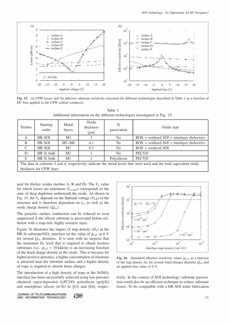
The extracted line loss and effective substrate resistivity as
a function of the DC bias applied to the central conductor
of a CPW line are, respectively, presented in Figs. 15(a) and
15(b) for different substrates, oxide layers and metallic lines
as summarized in Table 1. Techno A and B are wafers com-
ing from the industry while the three other wafers named
C, D and E are home processes with one metal layer. In all
cases, the metallic structures are patterned on either oxi-
dized p-type HR unibond SOI (techno A, B, C) or oxidized
p-type HR bulk Si (techno D and E) substrates.
The total RF losses (αtot ) of the CPW lines are extracted
from the measured S-parameters with a thru-line-reflect
method [62]. They are reported at 10 GHz in Fig. 15(a) as
a function of Va, where it is seen that αtot may be signifi-
cantly affected by Va when the oxide thickness (tox) is in the
several hundreds of nanometers (techno C). Indeed, in that
case highly positive or negative biases have a large impact
on the free carrier concentration below the oxide, thereby
strongly affecting substrate losses. This effect is attenu-
10
SOI Technology: An Opportunity for RF Designers?
Fig. 15. (a) CPW losses and (b) effective substrate resistivity measured for different technologies described in Table 1 as a function of
DC bias applied to the CPW central conductor.
Table 1
Additional information on the different technologies investigated in Fig. 15.
TechnoStarting
wafer
Metal
layers
Oxide
thickness
[µm]
Si
passivationOxide type
A HR SOI M3 3 No BOX + oxidized SOI + interlayer dielectrics
B HR SOI M5–M6 4.1 No BOX + oxidized SOI + interlayer dielectrics
C HR SOI M1 0.3 No BOX + oxidized SOI
D HR Si bulk M1 1 No PECVD
E HR Si bulk M1 1 Polysilicon PECVD
The data in columns 3 and 4, respectively, indicate the metal levels that were used and the total equivalent oxide
thickness for CPW lines.
ated for thicker oxides (techno A, B and D). The Va value
for which losses are minimum (Va,min) corresponds to the
state of deep depletion underneath the oxide. As shown in
Fig. 15, the Va depends on the flatband voltage (VFB) of the
structure and is therefore dependent on tox as well as the
oxide charge density (Qox).
The parasitic surface conduction can be reduced or even
suppressed if the silicon substrate is passivated before oxi-
dation with a trap-rich, highly resistive layer.
Figure 16 illustrates the impact of trap density (Dit ) at the
HR Si substrate/SiO2 interface on the value of ρe f f at 0 V
for several Qox densities. It is seen with no surprise that
the minimum Dit level that is required to obtain lossless
substrates (i.e., ρe f f = 10 kΩcm) is an increasing function
of the fixed charge density in the oxide. This is because for
higher positive densities, a higher concentration of electrons
is attracted near the substrate surface and a higher density
of traps is required to absorb those charges.
The introduction of a high density of traps at the Si/SiO2
interface has been successfully achieved using low-pressure
chemical vapor-deposited (LPCVD) polysilicon (polySi)
and amorphous silicon (α-Si) in [63] and [64], respec-
Fig. 16. Simulated effective resistivity values ρe f f as a function
of the trap density Dit for several fixed charges densities Qox and
an applied bias value of 0 V.
tively. In the context of SOI technology, substrate passiva-
tion could also be an efficient technique to reduce substrate
losses. To be compatible with a HR SOI wafer fabrication
11
Jean-Pierre Raskin
process, the passivation layer should be included within the
SOI structure by bonding an oxidized silicon wafer with
a passivated HR substrate.
In [65], the proposed method consists in the LPCVD-
deposition of amorphous silicon followed by Si-
crystallization at 900°C with RTA. This method was com-
pared with previously published techniques (passivation
with amorphous silicon in [64] or LPCVD-polysilicon
in [63] and was demonstrated to perform better in terms
of substrate loss reduction: effective resistivity values
higher than 10 kΩcm were reported, compared to 3 and
6 kΩcm in the case of amorphous Si and LPCVD polySi
passivation, respectively. The new passivation method
was also shown to present better rms surface roughness
(σ = 0.37 nm) and to remain effective after long thermal
anneals (4 hours at 900°C). A successful bonding of this
layer with an oxidized substrate was achieved, showing that
this new passivation technique could be introduced at re-
duced cost inside a smartcut or BESOI process in order to
fabricate SOI wafers with enhanced resistivity, i.e., higher
than 10 kΩcm.
Figure 15(a) indicates that substrate passivation with
polysilicon (techno E) significantly reduces RF losses while
getting rid of the Va influence. This is because traps present
inside the polySi layer can absorb free carriers and pin the
surface potential to a value independent on Va [63]. Fig-
ure 15(b) presents the effective resistivity (ρe f f ) extracted
according to a method depicted in [55]. Not surprisingly,
the highest ρe f f value is observed for the passivated sub-
strate, while at 0 V, the lowest value is obtained for the
low quality (Qox-rich) PECVD oxide. It should also be
noticed that due to the inverted layer underneath the BOX
in techno A and B, the extracted values of ρe f f do not ex-
ceed 130 and 580 Ωcm, respectively. These values are both
more than one order of magnitude lower than the nominal
substrate resistivity.
5.2. Crosstalk
In recent years, rapid progress of integrated circuit tech-
nology has enabled the co-integration of analog front-end
and digital baseband processing circuits of communication
systems onto the same chip. Such mixed-signal systems-on-
chip (SoCs) allow more functionality, higher performance,
lower power and higher reliability than non-integrated so-
lutions, where at least two chips are needed, one for digital
and one for the analog applications. Moreover, thanks to
CMOS technology scaling and its associated increasing in-
tegration level, SoCs have become the way to achieve cost
effectiveness for demanding applications such as home en-
tertainment and graphics, mobile consumer devices, net-
working and storage equipment.
Such a rising integration level of mixed-signal ICs raises
new issues for circuit designers. One of these issues is the
substrate noise (Fig. 19(a)) generated by switching digital
circuits, called digital substrate noise (DSN), which may
degrade the behavior of adjacent analog circuits [66].
DSN issues become more and more important with IC evo-
lution as
– digital parts get more noisy due to increasing com-
plexity and clock frequencies;
– digital and analog parts get closer;
– analog parts get more sensitive because of Vdd scaling
for power concern issues.
In general, substrate noise can be decomposed in three dif-
ferent mechanisms: noise generation, injection/propagation
into the substrate and reception by the analog part [67].
Improvement in the reduction of any of these three mech-
anisms, or in all of them, will lead to a reduction of the
DSN and in a relaxation of the design requirements. Typi-
cally, guard rings and overdesigned structures are adopted
to limit the effect of substrate noise, thereby reducing the
advantages of the introduction of new technologies. It is
thus a major issue for the semiconductor industry to find
area-efficient design/technology solutions to reduce the im-
pact of substrate noise in mixed-signal ICs.
This last decade several publications have demonstrated the-
oretically and experimentally the interest of high resistivity
SOI substrate to greatly reduce the crosstalk level between
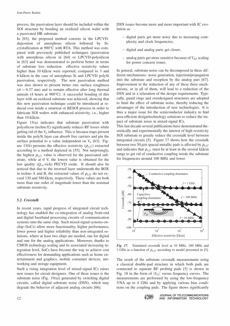
integrated circuits [5]. Figure 17 shows how the crosstalk
between two 50 µm spaced metallic pads is affected by ρe f f
and indicates that ρe f f must be at least in the several kΩcm
range to get rid of conductive coupling inside the substrate
for frequencies around 100 MHz and lower.
Fig. 17. Simulated crosstalk level at 10 MHz, 100 MHz and
1 GHz as a function of ρe f f according to model presented in [5].
The result of the substrate crosstalk measurements using
a classical double-pad structure in which both pads are
connected to separate RF probing pads [5] is shown in
Fig. 18 in the form of |S21| versus frequency curves. The
measurements are performed by using the low-frequency
VNA up to 4 GHz and by applying various bias condi-
tions on the coupling pads. The figure shows significantly
12
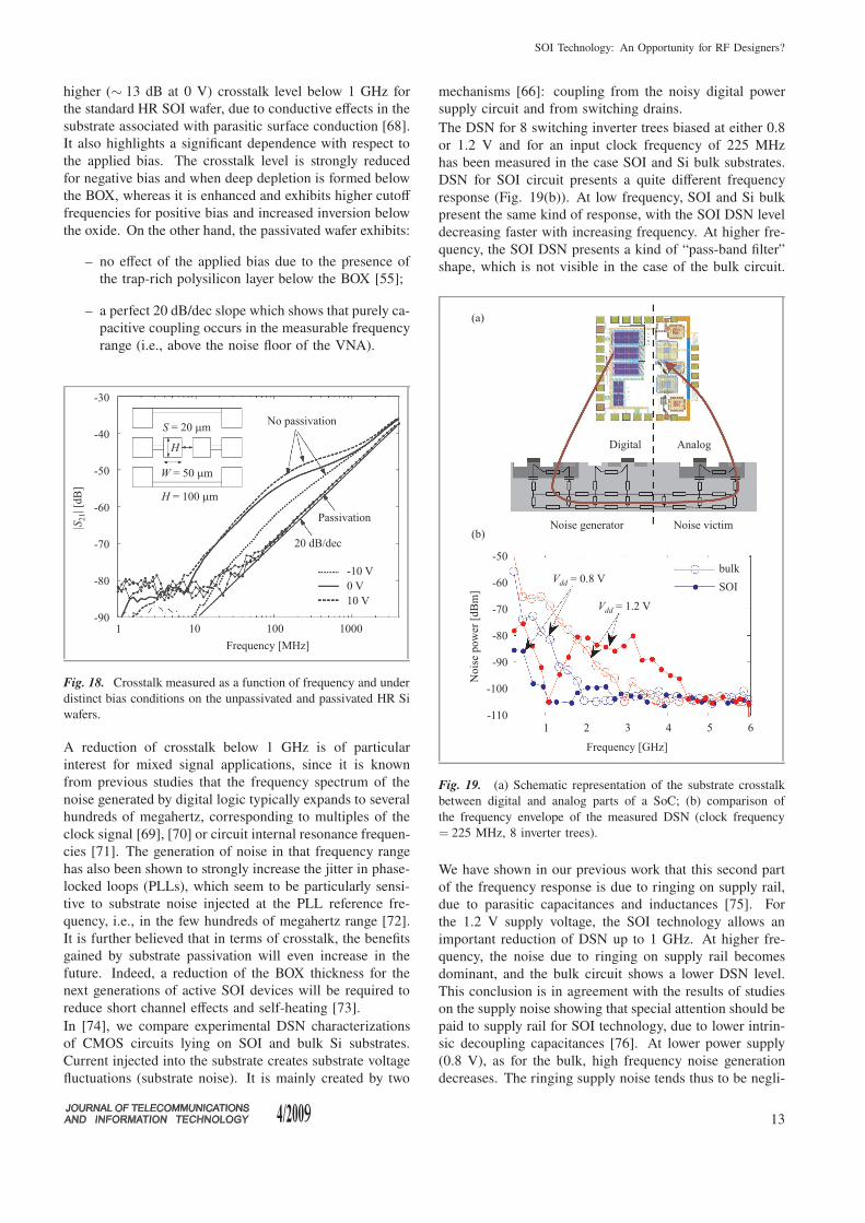
SOI Technology: An Opportunity for RF Designers?
higher (∼ 13 dB at 0 V) crosstalk level below 1 GHz for
the standard HR SOI wafer, due to conductive effects in the
substrate associated with parasitic surface conduction [68].
It also highlights a significant dependence with respect to
the applied bias. The crosstalk level is strongly reduced
for negative bias and when deep depletion is formed below
the BOX, whereas it is enhanced and exhibits higher cutoff
frequencies for positive bias and increased inversion below
the oxide. On the other hand, the passivated wafer exhibits:
– no effect of the applied bias due to the presence of
the trap-rich polysilicon layer below the BOX [55];
– a perfect 20 dB/dec slope which shows that purely ca-
pacitive coupling occurs in the measurable frequency
range (i.e., above the noise floor of the VNA).
Fig. 18. Crosstalk measured as a function of frequency and under
distinct bias conditions on the unpassivated and passivated HR Si
wafers.
A reduction of crosstalk below 1 GHz is of particular
interest for mixed signal applications, since it is known
from previous studies that the frequency spectrum of the
noise generated by digital logic typically expands to several
hundreds of megahertz, corresponding to multiples of the
clock signal [69], [70] or circuit internal resonance frequen-
cies [71]. The generation of noise in that frequency range
has also been shown to strongly increase the jitter in phase-
locked loops (PLLs), which seem to be particularly sensi-
tive to substrate noise injected at the PLL reference fre-
quency, i.e., in the few hundreds of megahertz range [72].
It is further believed that in terms of crosstalk, the benefits
gained by substrate passivation will even increase in the
future. Indeed, a reduction of the BOX thickness for the
next generations of active SOI devices will be required to
reduce short channel effects and self-heating [73].
In [74], we compare experimental DSN characterizations
of CMOS circuits lying on SOI and bulk Si substrates.
Current injected into the substrate creates substrate voltage
fluctuations (substrate noise). It is mainly created by two
mechanisms [66]: coupling from the noisy digital power
supply circuit and from switching drains.
The DSN for 8 switching inverter trees biased at either 0.8
or 1.2 V and for an input clock frequency of 225 MHz
has been measured in the case SOI and Si bulk substrates.
DSN for SOI circuit presents a quite different frequency
response (Fig. 19(b)). At low frequency, SOI and Si bulk
present the same kind of response, with the SOI DSN level
decreasing faster with increasing frequency. At higher fre-
quency, the SOI DSN presents a kind of “pass-band filter”
shape, which is not visible in the case of the bulk circuit.
Fig. 19. (a) Schematic representation of the substrate crosstalk
between digital and analog parts of a SoC; (b) comparison of
the frequency envelope of the measured DSN (clock frequency
= 225 MHz, 8 inverter trees).
We have shown in our previous work that this second part
of the frequency response is due to ringing on supply rail,
due to parasitic capacitances and inductances [75]. For
the 1.2 V supply voltage, the SOI technology allows an
important reduction of DSN up to 1 GHz. At higher fre-
quency, the noise due to ringing on supply rail becomes
dominant, and the bulk circuit shows a lower DSN level.
This conclusion is in agreement with the results of studies
on the supply noise showing that special attention should be
paid to supply rail for SOI technology, due to lower intrin-
sic decoupling capacitances [76]. At lower power supply
(0.8 V), as for the bulk, high frequency noise generation
decreases. The ringing supply noise tends thus to be negli-
13
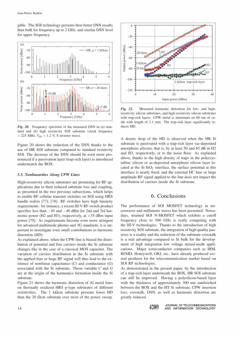
Jean-Pierre Raskin
gible. The SOI technology presents then better DSN results
than bulk for frequency up to 2 GHz, and similar DSN level
for upper frequency.
Fig. 20. Frequency spectrum of the measured DSN in (a) stan-
dard and (b) high resistivity SOI substrate (clock frequency
= 225 MHz, Vdd = 1.2 V, 8 inverter trees).
Figure 20 shows the reduction of the DSN thanks to the
use of HR SOI substrate compared to standard resistivity
SOI. The decrease of the DSN should be even more pro-
nounced if a passivation layer (trap-rich layer) is introduced
underneatch the BOX.
5.3. Nonlinearities Along CPW Lines
High-resistivity silicon substrates are promising for RF ap-
plications due to their reduced substrate loss and coupling,
as presented in the two previous subsections, which helps
to enable RF cellular transmit switches on SOI using HRS
handle wafers [77], [78]. RF switches have high linearity
requirements: for instance, a recent III-V RF switch product
specifies less than −45 and −40 dBm for 2nd and 3rd har-
monic power (H2 and H3), respectively, at +35 dBm input
power [79]. As requirements become even more stringent
for advanced multimode phones and 3G standards, it is im-
portant to investigate even small contributions to harmonic
distortion (HD).
As explained above, when the CPW line is biased the distri-
bution of potential and free carriers inside the Si substrate
changes like in the case of a classical MOS capacitor. The
variation of carriers distribution in the Si substrate with
the applied bias or large RF signal will thus lead to the ex-
istence of nonlinear capacitance (C) and conductance (G)
associated with the Si substrate. Those variable C and G
are at the origin of the harmonics formation inside the Si
substrate.
Figure 21 shows the harmonic distortion of Al metal lines
on thermally oxidized HRS p-type substrates of different
resistivities. The 1 kΩcm substrate presents lower HD
than the 20 Ωcm substrate over most of the power sweep.
Fig. 21. Measured harmonic distortion for low- and high-
resistivity silicon substrates, and high-resistivity silicon substrates
with trap-rich layers. CPW metal is aluminum on 60 nm of ox-
ide with length of 2.1 mm. The trap-rich layer significantly re-
duces HD.
A drastic drop of the HD is observed when the HR Si
substrate is passivated with a trap-rich layer (as-deposited
amorphous silicon), that is, by at least 50 and 65 dB in H2
and H3, respectively, or to the noise floor. As explained
above, thanks to the high density of traps in the polycrys-
talline silicon or as-deposited amorphous silicon layer lo-
cated at the Si-SiO2 interface, the surface potential at this
interface is nearly fixed, and the external DC bias or large
amplitude RF signal applied to the line does not impact the
distribution of carriers inside the Si substrate.
6. Conclusions
The performance of SOI MOSFET technology in mi-
crowaves and millimeter waves has been presented. Nowa-
days, strained SOI N-MOSFET which exhibits a cutoff
frequency close to 500 GHz is really competing with
the III-V technologies. Thanks to the introduction of high
resistivity SOI substrate, the integration of high quality pas-
sives is a reality and the reduction of the substrate crosstalk
is a real advantage compared to Si bulk for the develop-
ment of high integration low voltage mixed-mode appli-
cations. Major semiconductor companies such as IBM,
RFMD, Honeywell, OKI, etc., have already produced sev-
eral products for the telecommunication market based on
SOI RF technologies.
As demonstrated in the present paper, by the introduction
of a trap-rich layer underneath the BOX, HR SOI substrate
can still be improved. Having a polysilicon-based layer
with the thickness of approximately 300 nm sandwiched
between the BOX and the HT Si substrate, CPW insertion
loss, crosstalk, DSN, as well as harmonic distortion are
greatly reduced.
14
SOI Technology: An Opportunity for RF Designers?
To summarize, present and future HR SOI MOSFET tech-
nologies are very good candidatea for mixed-mode low volt-
age low power RF and even millimeter waves applications.
References
[1] G. E. Moore, “Cramming more components onto integrated circuits”,
Electronics, vol. 38, pp. 114–117, 1965.
[2] R. H. Dennard, F. H. Gaensslen, H.-N. Yu, V. L. Rideout, E. Bas-
sous, and A. R. Leblanc, “Design of ion-implanted MOSFET’s
with very small physical dimensions”, IEEE J. Solid-State Circ.,
vol. SC-9, pp. 256–268, 1974.
[3] S. Lee, B. Jagannathan, S. Narasimha, A. Chou, N. Zamdmer,
J. Johnson, R. Williams, L. Wagner, J. Kim, J.-O. Plouchart,
J. Pekarik, S. Springer, and G. Freeman, “Record RF performance
of 45-nm SOI CMOS technology”, in Proc. IEEE Int. Electron Dev.
Meet. IEDM 2007, Washington, USA, 2007, pp. 255–258.
[4] T. Sakurai, A. Matsuzawa, and T. Douseki, Fully-Depleted SOI
CMOS Circuits and Technology for Ultralow-Power Applications.
New Jersey: Springer, 2006.
[5] J.-P. Raskin, A. Viviani, D. Flandre, and J.-P. Colinge, “Substrate
crosstalk reduction using SOI technology”, IEEE Trans. Electron
Dev., vol. 44, no. 12, pp. 2252–2261, 1997.
[6] H. F. Cooke, “Microwave transistors: theory and design”, Proc.
IEEE, vol. 59, pp. 1163–1181, 1971.
[7] C. A. Mead, “Schottky barrier gate field effect transistor”, Proc.
IEEE, vol. 59, pp. 307–308, 1966.
[8] W. Baechtold, K. Daetwyler, T. Forster, T. O. Mohr, W. Walter,
and P. Wolf, “Si and GaAs 0.5 µm gate Schottky-barrier field-effect
transistors”, Electron. Lett., vol. 9, pp. 232–234, 1973.
[9] T. Mimura, S. Hiyamizu, T. Fujii, and K. Nanbu, “A new field-effect
transistor with selectively doped GaAs/n-AlxGa1−xAs heterojunc-
tions”, Jpn. J. Appl. Phys., vol. 19, pp. L225–L227, 1980.
[10] P. M. Smith, S.-M. J. Liu, M.-Y. Kao, P. Ho, S. C. Wang,
K. H. G. Duh, S. T. Fu, and P. C. Chao, “W-band high efficiency
InP-based power HEMT with 600 GHz fmax”, IEEE Microw. Guid.
Wave Lett., vol. 5, no. 7, pp. 230–232, 1995.
[11] M. J. W. Rodwell, M. Urteaga, T. Mathew, D. Scott, D. Mensa,
Q. Lee, J. Guthrie, Y. Betser, S. C. Martin, R. P. Smith, S. Ja-
ganathan, S. Krishnan, S. I. Long, R. Pullela, B. Agarwal, U. Bhat-
tacharya, L. Samoska, and M. Dahlstrom, “Submicron scaling
of HBTs”, IEEE Trans. Electron Dev., vol. 48, pp. 2606–2624, 2001.
[12] R. Lai, X. B. Mei, W. R. Deal, W. Yoshida, Y. M. Kim, P. H. Liu,
J. Lee, J. Uyeda, V. Radisic, M. Lange, T. Gaier, L. Samoska, and
A. Fung, “Sub 50 nm InP HEMT device with fmax greater than
1 THz”, in Proc. IEEE Int. Electron Dev. Meet. IEDM 2007, Wash-
ington, USA, 2007, pp. 609–611.
[13] H. S. Momose, E. Morifuji, T. Yoshitomi, T. Ohguro, I. Saito, T. Mo-
rimoto, Y. Katsumata, and H. Iwai, “High-frequency AC character-
istics of 1.5 nm gate oxide MOSFETs”, in Proc. IEEE Int. Electron
Dev. Meet. IEDM 1996, San Francisco, USA, 1996, pp. 105–108.
[14] “International Technology Roadmap for Semiconductors”, 2006,
[Online]. Available: http://www.itrs.net/Common/2006ITRS/
Home2006.html
[15] G. Dambrine, C. Raynaud, D. Lederer, M. Dehan, O. Rozeaux,
M. Vanmackelberg, F. Danneville, S. Lepilliet, and J.-P. Raskin,
“What are the limiting parameters of deep-submicron MOSFETs for
high frequency applications?”, IEEE Electron Dev. Lett., vol. 24,
no. 3, pp. 189–191, 2003.
[16] G. Pailloncy, C. Raynaud, M. Vanmackelberg, F. Danneville, S. Lep-
illiet, J.-P. Raskin, and G. Dambrine, “Impact of down scaling on
high frequency noise performance of bulk and SOI MOSFETs”,
IEEE Trans. Electron Dev., vol. 51, no. 10, pp. 1605–1612, 2004.
[17] V. Kilchytska, A. Neve, L. Vancaillie, D. Levacq, S. Adriaensen,
H. van Meer, K. De Mayer, C. Raynaud, M. Dehan, J.-P. Raskin,
and D. Flandre, “Influence of device engineering on the analog and
RF performances of SOI MOSFETs”, IEEE Trans. Electron Dev.,
vol. 50, no. 3, pp. 577–588, 2003.
[18] M. Vanmackelberg, C. Raynaud, O. Faynot, J.-L. Pelloie, C. Tabone,
A. Grouillet, F. Martin, G. Dambrine, L. Picheta, E. Mackowiak,
P. Llinares, J. Sevenhans, E. Compagne, G. Fletcher, D. Flandre,
V. Dessard, D. Vanhoenacker, and J.-P. Raskin, “0.25 µm fully-
depleted SOI MOSFET’s for RF mixed analog-digital circuits, in-
cluding a comparison with partially-depleted devices for high fre-
quency noise parameters”, Solid-State Electron., vol. 46, iss. 3,
pp. 379–386, 2002.
[19] S. Burignat, D. Flandre, V. Kilchytska, F. Andrieux, O. Faynot, and
J.-P. Raskin, “Substrate impact on sub-32 nm ultra thin SOI MOS-
FETs with thin buried oxide”, in Proc EUROSOI 2009, Fifth Worksh.
Them. Netw. Sil. Insul. Technol. Dev. Circ., Göteborg, Sweden, 2009,
pp. 27–28.
[20] T. Rudenko, V. Kilchytska, S. Burignat, J.-P. Raskin, F. Andrieu,
O. Faynot, A. Nazarov, and D. Flandre, “Transconductance and
mobility behaviors in UTB SOI MOSFETs with standard and thin
BOX”, in Proc. EUROSOI 2009, Fifth Worksh. Them. Netw. Sil.
Insul. Technol. Dev. Circ., Göteborg, Sweden, 2009, pp. 111–112.
[21] K.-W. Ang, J. Lin, C.-H. Tung, N. Balasubramanian, G. S. Samudra,
and Y.-C. Yeo, “Strained n-MOSFET with embedded source/drain
stressors and strain-transfer structure (STS) for enhanced transis-
tor performance”, IEEE Trans. Electron Dev., vol. 55, no. 3,
pp. 850–857, 2008.
[22] G. Néau, F. Martinez, M. Valenza, J. C. Vildeuil, E. Vincent,
F. Boeuf, F. Payet, and K. Rochereau, “Impact of strained-channe
n-MOSFETs with a SiGe virtual substrate on dielectric interface
quality evaluated by low frequency noise measurements”, Micro-
electron. Reliab., vol. 47, pp. 567–572, 2007.
[23] S. H. Olsen, E. Escobedo-Cousin, J. B. Varzgar, R. Agaiby,
J. Seger, P. Dobrosz, S. Chattopadhyay, S. J. Bull, A. G. O’Neill,
P.-E. Hellstrom, J. Edholm, M. Ostling, K. L. Lyutovich, M. Oehme,
and E. Kasper, “Control of self-heating in thin virtual substrate
strained Si MOSFETs”, IEEE Trans. Electron Dev., vol. 53, no. 9,
pp. 2296–2305, 2006.
[24] J. M. Larson and J. Snyder, “Overview and status of metal S/D
Schottky barrier MOSFET technology”, IEEE Trans. Electron Dev.,
vol. 53, no. 5, pp. 1048–1058, 2006.
[25] D. J. Pearman, G. Pailloncy, J.-P. Raskin, J. M. Larson, and
T. E. Whall, “Static and high-frequency behavior and performance
of Schottky barrier p-MOSFET devices”, IEEE Trans. Electron Dev.,
vol. 54, no. 10, pp. 2796–2802, 2007.
[26] J.-P. Raskin, D. J. Pearman, G. Pailloncy, J. M. Larson, J. Snyder,
D. L. Leadley, and T. E. Whall, “High-frequency performance of
Schottky barrier p-MOSFET devices”, IEEE Electron Dev. Lett.,
vol. 29, no. 4, pp. 396–398, 2008.
[27] G. Larrieu, E. Dubois, R. Valentin, N. Breil, F. Danneville,
G. Dambrine, J.-P. Raskin, and J.-C. Pesant, “Low temperature im-
plementation of dopant-segregated band-edge metallic S/D junctions
in thin-body SOI p-MOSFETs”, in Proc. IEEE Int. Electron Dev.
Meet. IEDM 2007, Washington, USA, 2007, pp. 147–150.
[28] R. Valentin, E. Dubois, J.-P. Raskin, G. Larrieu, G. Dambrine,
T. C. Lim, N. Breil, and F. Danneville, “RF small signal analysis of
Schottky-barrier p-MOSFET”, IEEE Trans. Electron Dev., vol. 55,
no. 5, pp. 1192–1202, 2008.
[29] B. Ricco, R. Versari, and D. Esseni, “Characterization of polysilicon-
gate depletion in MOS structures”, IEEE Electron Dev. Lett., vol. 17,
no. 3, pp. 103–105, 1996.
[30] A. Vandooren, A. V. Y. Thean, Y. Du, I. To, J. Hughes, T. Stephens,
M. Huang, S. Egley, M. Zavala, K. Sphabmixay, A. Barr, T. White,
S. Samavedam, L. Mathew, J. Schaeffer, D. Triyoso, M. Rossow,
D. Roan, D. Pham, R. Rai, B.-Y. Nguyen, B. White, M. Orlowski,
A. Duvallet, T. Dao, and J. Mogab, “Mixed-signal performance of
sub-100 nm fully-depleted SOI devices with metal gate, high K
(HfO2) dielectric and elevated source/drain extensions”, in Proc.
IEEE Int. Electron Dev. Meet. IEDM 2003, Washington, USA, 2003,
pp. 11.5.1–11.5.3.
[31] C. H. Ko, T. M. Kuan, K. Zhang, G. Tsai, S. M. Seutter, C. H. Wu,
T. J. Wang, C. N. Ye, H. W. Chen, C. H. Ge, K. H. Wu, and
W. C. Lee, “A novel CVD-SiBCN low-K spacer technology for
high-speed applications”, in Proc. Int. Symp. VLSI Technol. 2008,
Honolulu, Hawaii, USA, 2008, pp. 108–109.
15
Jean-Pierre Raskin
[32] T. I. Bao, H. C. Chen, C. J. Lee, H. H. Lu, S. L. Shue, and C. H. Yu,
“Low capacitance approaches for 22 nm generation Cu intercon-
nect”, in Proc. Int. Symp. VLSI Technol. Syst. Appl. VLSI-TSA 2009,
Hsinchu, Taiwan, 2009, pp. 51–56.
[33] T. Ernst, C. Tinella, C. Raynaud, and S. Cristoloveanu, “Fringing
fields in sub-0.1 µm fully depleted SOI MOSFET’s: optimization of
the device architecture”, Solid-State Electron., vol. 46, pp. 373–378,
2002.
[34] M. Fujiwara et al., “Impact of BOX scaling on 30 nm gate length
FD SOI MOSFET”, IEEE Int. SOI Conf., Honolulu, Hawaii, USA,
2005, pp. 180–182.
[35] F. Gianesello, D. Gloria, C. Raynaud, S. Montusclat, S. Boret,
C. Clement, P. Benech, J. M. Fournier, and G. Dambrine, “State of
the art 200 GHz passive components and circuits integrated in ad-
vanced thin SOI CMOS technology on high resistivity substrate”, in
Proc. IEEE Int. SOI Conf., Niagara Falls, USA, 2006, pp. 121–122.
[36] F. Gianesello, D. Gloria, C. Raynaud, S. Montusclat, S. Boret, and
P. Touret, “On the design of high performance RF integrated induc-
tors on high resistively thin film 65 nm SOI CMOS technology”,
in Proc. IEEE 8th Top. Meet. Sil. Monolit. Integr. Circ. RF Syst.
SiRF 2008, Orlando, USA, 2008, pp. 98–101.
[37] I. Post, M. Akbar, G. Curello, S. Gannavaram, W. Hafez, U. Jalan,
K. Komeyii, J. Lin, N. Lindert, J. Park, J. Rizk, G. Sacks, C. Tsai,
D. Yeh, P. Bai, and C.-H. Jan, “A 65 m CMOS SOC technology
featuring strained silicon transistors for RF applications”, in Proc.
Int. Electron Dev. Meet. IEDM 2006, San Francisco, USA, 2006,
pp. 1–3.
[38] J.-P. Colinge, M.-H. Gao, A. Romano, H. Maes, and C. Claeys,
“Silicon-on-insulator “gate-all-around” MOS device”, in Proc. IEEE
SOS/SOI Tech. Conf., Key West, USA, 1990, pp. 137–138.
[39] D. Hisamoto et al., “FinFET – a self-aligned double-gate MOSFET
scalable to 20 nm”, IEEE Trans. Electron Dev., vol. 47, no. 12,
pp. 2320–2325, 2000.
[40] S. Cristoloveanu, “Silicon on insulator technologies and devices:
from present to future”, Solid-State Electron., vol. 45, no. 8,
pp. 1403–1411, 2001.
[41] J.-T. Park and J.-P. Colinge, “Multiple-gate SOI MOSFETs: de-
vice design guidelines”, IEEE Trans. Electron Dev., vol. 49, no. 12,
pp. 2222–2229, 2002.
[42] J. Kedzierski et al., “High performance symmetric-gate and CMOS-
compatible Vt asymmetric-gate FinFET devices”, in Proc. IEEE
Int. Electron Dev. Meet. IEDM 2001, Washington, USA, 2001,
pp. 437–440.
[43] D. Woo et al., “Electrical characteristics of FinFET with vertically
nonuniform source/drain profile”, IEEE Trans. Nanotech., vol. 1,
no. 4, pp. 233–237, 2002.
[44] V. Kilchytska, N. Collaert, R. Rooyackers, D. Lederer, J.-P. Raskin,
and D. Flandre, “Perspective of FinFETs for analog applications”,
in Proc. 34th Eur. Solid-State Dev. Res. Conf. ESSDERC 2004, Leu-
ven, Belgium, 2004, pp. 65–68.
[45] D. Lederer et al., “FinFet analogue characterization from DC to
110 GHz”, Solild-State Electron., vol. 49, pp. 1488–1496, 2005.
[46] A. Dixit et al., “Analysis of the parasitic source/drain resistance in
multiple gate field effect transistors”, IEEE Trans. Electron Dev.,
vol. 52, no. 6, pp. 1131–1140, 2005.
[47] J. P. Raskin et al., “Accurate MOSFET characterization at microwa-
ver frequencies for device optimization and analog modeling”, IEEE
Trans. Electron Dev., vol. 45, pp. 1017–1025, 1998.
[48] A. Bracale et al., “A new approach for SOI device small-signal
parameter extraction”, Analog Integr. Circ. Sig. Process., vol. 25,
pp. 159–167, 2000.
[49] B. Razavi, R.-H. Yan, and K. F. Lee, “Impact of distributed gate
resistance on the performance of MOS devices”, IEEE Trans. Circ.
Syst. I: Fund. Theory Appl., vol. 41, no. 11, pp. 750–754, 1994.
[50] W. Wu and M. Chan, “Analysis of geometry-dependent parasitics in
multifin double-gate FinFETs”, IEEE Trans. Electron Dev., vol. 54,
no. 4, pp. 692–698, 2007.
[51] O. Moldovan, D. Lederer, B. Iniguez, and J.-P. Raskin, “Finite el-
ement simulations of parasitic capacitances related to multiple-gate
field-effect transistors architectures”, in Proc. 8th Top. Meet. Sil.
Monolit. Integr. Circ. RF Syst. SiRF 2008, Orlando, USA, 2008,
pp. 183–186.
[52] J.-P. Raskin, T. M. Chung, V. Kilchytska, D. Lederer, and D. Flan-
dre, “Analog/RF performance of multiple-gate SOI devices: wide-
band simulations and characterization”, IEEE Trans. Electron Dev.,
vol. 53, no. 5, pp. 1088–1094, 2006.
[53] J.-P. Raskin, G. Pailloncy, D. Lederer, F. Danneville, G. Dambrine,
S. Decoutere, A. Mercha, and B. Parvais, “High frequency noise
performance of 60 nm gate length FinFETs”, IEEE Trans. Electron
Dev., vol. 55, no. 10, pp. 2718–2727, 2008.
[54] F. Gianesello et al., “1.8 dB insertion loss 200 GHz CPW band pass
filter integrated in HR SOI CMOS technology”, in Proc. Conf. IEEE
MTT-S, Honolulu, Hawaii, USA, 2007.
[55] D. Lederer and J.-P. Raskin, “Effective resistivity of fully-processed
high resistivity wafers”, Solid-State Electron., vol. 49, pp. 491–496,
2005.
[56] W. Heinrich, “Quasi-TEM description of MMIC coplanar lines in-
cluding conductor-loss effects”, IEEE Trans. Microw. Theory Tech.,
vol. 41, no. 1, pp. 45–52, 1993.
[57] A. C. Reyes, S. M. El-Ghazaly, S. J. Dom, M. Dydyk,
D. K. Schroeder, and H. Patterson, “Coplanar waveguides and mi-
crowave inductors on silicon substrates”, IEEE Trans. Microw. The-
ory Tech., vol. 43, no. 9, pp. 2016–2021, 1995.
[58] K. Benaissa, J.-T. Yuan, D. Crenshaw, B. Williams, S. Sridhar, J. Ai,
G. Boselli, S. Zhao, S. Tang, S. Ashbun, P. Madhani, T. Blythe,
N. Mahalingam, and H. Schichijo, “RF CMOS high-resistivity sub-
strates for systems-on-chip applications”, IEEE Trans. Electron Dev.,
vol. 50, no. 3, pp. 567–576, 2003.
[59] Y. Wu, H. S. Gamble, B. M. Armstrong, V. F. Fusco, and
J. A. C. Stewart, “SiO2 interface layer effects on microwave loss of
high-resistivity CPW line”, IEEE Microw. Guid. Wave Lett., vol. 9,
no. 1, pp. 10–12, 1999.
[60] D. Lederer, C. Desrumeaux, F. Brunier, and J.-P. Raskin, “High
resistivity SOI substrates: how high should we go?”, in Proc. IEEE
Int. SOI Conf., Newport Beach, USA, 2003, pp. 50–51.
[61] C. Schollhorn, W. Zhao, M. Morschbach, and E. Kasper, “Attenua-
tion mechanisms of aluminum millimeter-wave coplanar waveguides
on silicon”, IEEE Trans. Electron Dev., vol. 50, no. 3, pp. 740–746,
2003.
[62] H.-C. Lu and T.-H. Chu, “The thru-line-symmetry (TLS) calibration
method for on-wafer scattering matrix measurement of four-port net-
works”, in Proc. IEEE MTT-S Int. Microw. Symp. Dig., Ford Worth,
USA, 2004, vol. 3, pp. 1801–1804.
[63] H. Gamble, B. M. Armstrong, S. J. N. Mitchell, Y. Wu, V. F. Fusco,
and J. A. C. Stewart, “Low-loss CPW lines on surface stabilized high
resistivity silicon”, IEEE Microw. Guid. Wave Lett., vol. 9, no. 10,
pp. 395–397, 1999.
[64] B. Wong, J. N. Burghartz, L. K. Natives, B. Rejaei, and M. van
der Zwan, “Surface-passivated high resistivity silicon substrates tor
RFICs”, IEEE Electron Dev. Lett., vol. 25, no. 4, pp. 176–178, 2004.
[65] D. Lederer and J.-P. Raskin, “New substrate passivation method
dedicated to high resistivity SOI wafer fabrication with increase
substrate resistivity”, IEEE Electron Dev. Lett., vol. 26, no. 11,
pp. 805–807, 2005.
[66] F. Calmon, C. Andrei, O. Valorge, J.-C. Nunez Perez, J. Verdier, and
C. Gontrand, “Impact of low-frequency substrate disturbances on
a 4.5 GHz VCO”, Microelectron. J., vol. 37, no. 1, pp. 1119–1127,
2006.
[67] M. van Heijningen, M. Badaroglu, S. Donnay, M. Engels, and
I. Bolsen, “High-level simulation of substrate noise generation in-
cluding power supply noise coupling”, in Proc. 37th Conf. Des.
Automat. DAC 2000, Los Angeles, USA, 2000, pp. 446–451.
[68] D. Lederer and J.-P. Raskin, “Bias effects on RF passive structures
in HR Si substrates”, in Proc. 6th Top. Meet. Sil. Microw. Integr.
Circ. RF Syst., San Diego, USA, 2006, pp. 8–11.
16
SOI Technology: An Opportunity for RF Designers?
[69] M. van Heijningen, J. Compiet, P. Wambacq, S. Donnay,
M. G. E. Engels, and I. Bolsens, “Analysis and experimental verifi-
cation of digital substrate noise generation for epi-type substrates”,
IEEE J. Solid-State Circ., vol. 35, no. 7, pp. 1002–1008, 2000.
[70] M. van Heijningen, M. Badaroglu, S. Donnay, G. G. E. Gielen,
and H. J. De Man, “Substrate noise generation in complex digital
systems: efficient modeling and simulation methodology and ex-
perimental verification”, IEEE J. Solid-State Circ., vol. 37, no. 8,
pp. 1065–1072, 2002.
[71] M. Badaroglu, S. Donnay, H. J. De Man, Y. A. Zinzius, G. G. E. Gie-
len, W. Sansen, T. Fonden, and S. Signell, “Modeling and experi-
mental verification of substrate noise generation in a 220-k gates
WLAN system-on-chip with multiple supplies”, IEEE J. Solid-State
Circ., vol. 38, no. 7, pp. 1250–1260, 2003.
[72] K. A. Jenkins, W. Rhee, J. Liobe, and H. Ainspan, “Experimental
analysis of the effect of substrate noise on PLL”, in Proc. 6th Top.
Meet. Sil. Monolit. Integr. Circ. RF Syst., San Diego, USA, 2006,
pp. 54–57.
[73] “International Technology Roadmap for Semiconductors: Front end
processes”, 2005 [Online]. Available: http://www.itrs.net/Common/
2005ITRS/FEP2005.pdf
[74] C. Roda Neve, D. Bol, R. Ambroise, D. Flandre, and J.-P. Raskin,
“Comparison of digital substrate noise in SOI and bulk Si CMOS
technologies”, in Proc. 7th Worksh. Low-Volt. Low Power Des.,
Louvain-la-Neuve, Belgium, 2008, pp. 23–28.
[75] D. Bol, R. Ambroise, C. Roda Neve, J.-P. Raskin, and D. Flandre,
“Wide-band simulation and characterization of digital substrate noise
in SOI technology”, in Proc. IEEE Int. SOI Conf., Indian Wells,
USA, 2007, pp. 133–134.
[76] H. H. Chen and D. D. Ling, “Power supply noise analysis method-
ology for deep-submicron VLSI chip design”, in Proc. 34th Des.
Automat., Anaheim, USA, 1997, pp. 638–643.
[77] C. Tinella, O. Richard, A. Cathelin, F. Reaute, S. Majcherczak,
F. Blanchet, and D. Belot, “0.13 µm CMOS SOI SP6T antenna
switch for multi-standard handsets”, in Proc. 6th Top. Meet. Sil.
Monolit. Integr. Circ. RF Syst., San Diego, USA, 2006, p. 58.
[78] T. G. McKay, M. S. Carroll, J. Costa, C. Iversen, D. C. Kerr, and
Y. Remoundos, “Linear cellular antenna switch for highly integrated
SOI front-end”, in Proc. IEEE Int. SOI Conf., Indian Wells, USA,
2007.
[79] “Single-pole four-throw high-power switch”, RF1450 Data sheet
[Online]. Available: http://www.rfmd.com/pdfs/1450DS.pdf
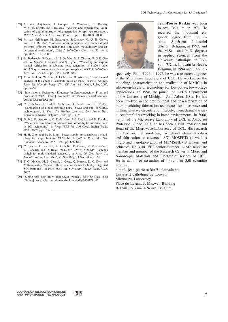
Jean-Pierre Raskin was born
in Aye, Belgium, in 1971. He
received the industrial en-
gineer degree from the In-
stitut Supérieur Industriel
d’Arlon, Belgium, in 1993, and
the M.Sc. and Ph.D. degrees
in applied sciences from the
Université catholique de Lou-
vain (UCL), Louvain-la-Neuve,
Belgium, in 1994 and 1997, re-
spectively. From 1994 to 1997, he was a research engineer
at the Microwave Laboratory of UCL. He worked on the
modeling, characterization and realization of MMIC’s in
silicon-on-insulator technology for low-power, low-voltage
applications. In 1998, he joined the EECS Department
of the University of Michigan, Ann Arbor, USA. He has
been involved in the development and characterization of
micromachining fabrication techniques for microwave and
millimeter-wave circuits and microelectromechanical trans-
ducers/amplifiers working in harsh environments. In 2000,
he joined the Microwave Laboratory of UCL as Associate
Professor. Since 2007, he has been a Full Professor and
Head of the Microwave Laboratory of UCL. His research
interests are the modeling, wideband characterization
and fabrication of advanced SOI MOSFETs as well as
micro and nanofabrication of MEMS/NEMS sensors and
actuators. He is an IEEE senior member, EuMA associate
member and member of the Research Center in Micro and
Nanoscopic Materials and Electronic Devices of UCL.
He is author or co-author of more than 350 scientific
articles.
e-mail: [email protected]
Université catholique de Louvain
Microwave Laboratory
Place du Levant, 3, Maxwell Building
B-1348 Louvain-la-Neuve, Belgium
17