Embed Size (px)
Citation preview

SN75161B, SN75162BOCTAL GENERAL-PURPOSE INTERFACE BUS TRANSCEIVERS
SLLS005B – OCTOBER 1980 – REVISED MAY 1995
1POST OFFICE BOX 655303 • DALLAS, TEXAS 75265
Meets IEEE Standard 488-1978 (GPIB)
8-Channel Bidirectional Transceivers
Power-Up/Power-Down Protection(Glitch Free)
Designed to Implement Control BusInterface
SN75161B Designed for Single Controller
SN75162B Designed for MultipleControllers
High-Speed, Low-Power Schottky Circuitry
Low Power Dissipatio n . . . 72 mW Max PerChannel
Fast Propagation Times . . . 22 ns Max
High-Impedance pnp Inputs
Receiver Hysteresi s . . . 650 mV Typ
Bus-Terminating Resistors Provided onDriver Outputs
No Loading of Bus When Device IsPowered Down (V CC = 0)
description
The SN75161B and SN75162B eight-channel,general-purpose interface bus transceivers aremonolithic, high-speed, low-power Schottkydevices designed to meet the requirements ofIEEE Standard 488-1978. Each transceiver isdesigned to provide the bus-management anddata-transfer signals between operating units ofa single- or multiple-controller instrumentationsystem. When combined with the SN75160B octalbus transceiver, the SN75161B or SN75162Bprovides the complete 16-wire interface for theIEEE-488 bus.
The SN75161B and SN75162B feature eightdriver-receiver pairs connected in a front-to-backconfiguration to form input/output (I/O) ports atboth the bus and terminal sides. A power-up/-down disable circuit is included on all bus andreceiver outputs. This provides glitch-free opera-tion during VCC power up and power down.
Copyright 1995, Texas Instruments IncorporatedPRODUCTION DATA information is current as of publication date.Products conform to specifications per the terms of Texas Instrumentsstandard warranty. Production processing does not necessarily includetesting of all parameters.
Please be aware that an important notice concerning availability, standard warranty, and use in critical applications ofTexas Instruments semiconductor products and disclaimers thereto appears at the end of this data sheet.
SCTE
RENIFC
NDACNRFD
DAVEOIATNSRQ
NCGND
1
2
3
4
5
6
7
8
9
10
11
22
21
20
19
18
17
16
15
14
13
12
VCCNCRENIFCNDACNRFDDAVEOIATNSRQNCDC
(TOP VIEW)
TERENIFC
NDACNRFD
DAVEOIATNSRQGND
VCCRENIFCNDACNRFDDAVEOIATNSRQDC
1
2
3
4
5
6
7
8
9
10
20
19
18
17
16
15
14
13
12
11
GPIBI/O Ports
TerminalI/O Ports
(TOP VIEW)
1
2
3
4
5
6
7
8
9
10
11
12
24
23
22
21
20
19
18
17
16
15
14
13
SCTE
RENIFC
NDACNRFD
DAVEOIATNSRQGND
VCCNCRENIFCNDACNRFDDAVEOIATNSRQDC
(TOP VIEW)
NC–No internal connection
SN75161B . . . DW OR N PACKAGE
SN75162B . . . DW PACKAGE
SN75162B . . . N PACKAGE
GPIBI/O Ports
TerminalI/O Ports
GPIBI/O Ports
TerminalI/O Ports
SN75161B, SN75162BOCTAL GENERAL-PURPOSE INTERFACE BUS TRANSCEIVERS
SLLS005B – OCTOBER 1980 – REVISED MAY 1995
2 POST OFFICE BOX 655303 • DALLAS, TEXAS 75265
description (continued)
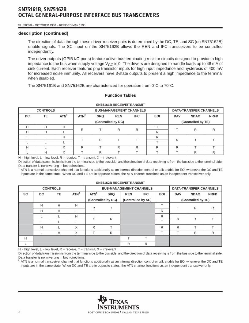
The direction of data through these driver-receiver pairs is determined by the DC, TE, and SC (on SN75162B)enable signals. The SC input on the SN75162B allows the REN and IFC transceivers to be controlledindependently.
The driver outputs (GPIB I/O ports) feature active bus-terminating resistor circuits designed to provide a highimpedance to the bus when supply voltage VCC is 0. The drivers are designed to handle loads up to 48 mA ofsink current. Each receiver features pnp transistor inputs for high input impedance and hysteresis of 400 mVfor increased noise immunity. All receivers have 3-state outputs to present a high impedance to the terminalwhen disabled.
The SN75161B and SN75162B are characterized for operation from 0°C to 70°C.
Function Tables
SN75161B RECEIVE/TRANSMIT
CONTROLS BUS-MANAGEMENT CHANNELS DATA-TRANSFER CHANNELS
DC TE ATN† ATN† SRQ REN IFC EOI DAV NDAC NRFD
(Controlled by DC) (Controlled by TE)
H H HR T R R
TT R R
H H LR T R R
RT R R
L L HT R T T
RR T T
L L LT R T T
TR T T
H L X R T R R R R T T
L H X T R T T T T R R
H = high level, L = low level, R = receive, T = transmit, X = irrelevantDirection of data transmission is from the terminal side to the bus side, and the direction of data receiving is from the bus side to the terminal side.Data transfer is noninverting in both directions.† ATN is a normal transceiver channel that functions additionally as an internal direction control or talk enable for EOI whenever the DC and TE
inputs are in the same state. When DC and TE are in opposite states, the ATN channel functions as an independent transceiver only.
SN75162B RECEIVE/TRANSMIT
CONTROLS BUS-MANAGEMENT CHANNELS DATA-TRANSFER CHANNELS
SC DC TE ATN† ATN† SRQ REN IFC EOI DAV NDAC NRFD
(Controlled by DC) (Controlled by SC) (Controlled by TE)
H H HR T
TT R R
H H LR T
RT R R
L L HT R
RR T T
L L LT R
TR T T
H L X R T R R T T
L H X T R T T R R
H T T
L R R
H = high level, L = low level, R = receive, T = transmit, X = irrelevantDirection of data transmission is from the terminal side to the bus side, and the direction of data receiving is from the bus side to the terminal side.Data transfer is noninverting in both directions.† ATN is a normal transceiver channel that functions additionally as an internal direction control or talk enable for EOI whenever the DC and TE
inputs are in the same state. When DC and TE are in opposite states, the ATN channel functions as an independent transceiver only.

SN75161B, SN75162BOCTAL GENERAL-PURPOSE INTERFACE BUS TRANSCEIVERS
SLLS005B – OCTOBER 1980 – REVISED MAY 1995
3POST OFFICE BOX 655303 • DALLAS, TEXAS 75265
CHANNEL-IDENTIFICATION TABLE
NAME IDENTITY CLASS
DC Direction Control
TE Talk Enable Control
SC System Control (SN75162B only)
ATN Attention
SRQ Service Request
REN Remote Enable Bus
IFC Interface Clear Management
EOI End of Identity
DAV Data Valid
NDAC Not Data Accepted Data
NRFD Not Ready for Data Transfer
SN75161B logic symbol †
EN31
ATN8
1
ATN13
11
EOI7
3
EOI14
13
SRQ
1
SRQ12
1
1
REN2
1
REN19
11
IFC3
1
IFC18
1
1
DAV6
2
DAV15
12
NDAC4
2
NDAC17
12
21
16NRFD
2
EN1/G4
EN2/G5
5
4
5NRFD
TE1
DC11
This symbol is in accordance with IEEE Std 91-1984 and IEC Publication 617-12.Designates 3-state outputsDesignates passive-pullup outputs
9
SN75161B logic diagram (positive logic)
NRFD5NRFD 16
NDAC4NDAC 17
DAV6DAV 15
IFC3IFC18
REN2REN 19
SRQ9SRQ 12
EOI7EOI14
11DC
1TE
13ATN 8 ATN

SN75161B, SN75162BOCTAL GENERAL-PURPOSE INTERFACE BUS TRANSCEIVERS
SLLS005B – OCTOBER 1980 – REVISED MAY 1995
4 POST OFFICE BOX 655303 • DALLAS, TEXAS 75265
SN75162B logic symbol †
EN3≥ 1
ATN1
ATN14
11
EOI6
EOI1
6
SRQ
1
SRQ
1
1
RENREN
13
IFCIFC
1DAV
2
DAV
12
NDAC
2
NDAC
1
2
21
NRFD
2
EN1/G4
EN2/G5
5
4
NRFD
TE
DC
This symbol is in accordance with IEEE Std 91-1984 and IEC Publication 617-12.Designates 3-state outputsDesignates passive-pullup outputs
EN3
12
2
1
15
SC
13
20
19
16
18
17
9
8
10
3
4
7
5
6
3
33
Pin numbers shown are for the N package.
SN75162B logic diagram (positive logic)
NRFDNRFD
NDACNDAC
DAVDAV
IFCIFC
RENREN
SRQSRQ
EOIEOI
DC
TE
ATN ATN
12
2
1
14
15
13
20
19
16
18
17
9
8
10
3
4
7
5
6
SC

SN75161B, SN75162BOCTAL GENERAL-PURPOSE INTERFACE BUS TRANSCEIVERS
SLLS005B – OCTOBER 1980 – REVISED MAY 1995
5POST OFFICE BOX 655303 • DALLAS, TEXAS 75265
schematics of inputs and outputs
NOM4 kΩ
R(eq) 1.7 kΩNOM
10 kΩNOM
VCC
GND
Input/Output Port
Input/Output Port
GND
VCC
NOM10 kΩ
NOM4 kΩ
NOM1.7 kΩ
NOM9 kΩ
GND
Input
VCC
NOM4 kΩ
EQUIVALENT OF ALL CONTROL INPUTS TYPICAL OF SRQ, NDAC, AND NRFD GPIB I/O PORT
Circuit inside dashed lines is on the driver outputs only.
TYPICAL OF ALL I/O PORTS EXCEPT SRQ, NDAC,AND NRFD GPIB I/O PORTS
Driver output R (eq) = 30 Ω NOMReceiver output R (eq) = 110 Ω NOMCircuit inside dashed lines is on the driver outputs only.R(eq) = equivalent resistor
absolute maximum ratings over operating free-air temperature range (unless otherwise noted) †
Supply voltage, VCC (see Note 1) 7 V. . . . . . . . . . . . . . . . . . . . . . . . . . . . . . . . . . . . . . . . . . . . . . . . . . . . . . . . . . . . . Input voltage, VI 5.5 V. . . . . . . . . . . . . . . . . . . . . . . . . . . . . . . . . . . . . . . . . . . . . . . . . . . . . . . . . . . . . . . . . . . . . . . . . . Low-level driver output current, IOL 100 mA. . . . . . . . . . . . . . . . . . . . . . . . . . . . . . . . . . . . . . . . . . . . . . . . . . . . . . . . Continuous total power dissipation See Dissipation Rating Table. . . . . . . . . . . . . . . . . . . . . . . . . . . . . . . . . . . . . Operating free-air temperature range, TA 0°C to 70°C. . . . . . . . . . . . . . . . . . . . . . . . . . . . . . . . . . . . . . . . . . . . . . Storage temperature range, Tstg –65°C to 150°C. . . . . . . . . . . . . . . . . . . . . . . . . . . . . . . . . . . . . . . . . . . . . . . . . . . Lead temperature 1,6 mm (1/16) inch from the case for 10 seconds 260°C. . . . . . . . . . . . . . . . . . . . . . . . . . . .
† Stresses beyond those listed under “absolute maximum ratings” may cause permanent damage to the device. These are stress ratings only, andfunctional operation of the device at these or any other conditions beyond those indicated under “recommended operating conditions” is notimplied. Exposure to absolute-maximum-rated conditions for extended periods may affect device reliability.
NOTE 1: All voltage values are with respect to network ground terminal.

SN75161B, SN75162BOCTAL GENERAL-PURPOSE INTERFACE BUS TRANSCEIVERS
SLLS005B – OCTOBER 1980 – REVISED MAY 1995
6 POST OFFICE BOX 655303 • DALLAS, TEXAS 75265
DISSIPATION RATING TABLE
PACKAGETA ≤ 25°C
POWER RATINGDERATING FACTORABOVE TA = 25°C
TA = 70°CPOWER RATING
DW (20 pin) 1125 mW 9.0 mW/°C 720 mW
DW (24 pin) 1350 mW 10.8 mW/°C 864 mW
N (20 pin) 1150 mW 9.2 mW/°C 736 mW
N (22 pin) 1700 mW 13.6 mW/°C 1088 mW
recommended operating conditions
MIN NOM MAX UNIT
Supply voltage, VCC 4.75 5 5.25 V
High-level input voltage, VIH 2 V
Low-level input voltage, VIL 0.8 V
High level output current IOHBus ports with 3-state outputs –5.2 mA
High-level output current, IOHTerminal ports –800 µA
Low level output current IOLBus ports 48
mALow-level output current, IOLTerminal ports 16
mA
Operating free-air temperature, TA 0 70 °C

SN75161B, SN75162BOCTAL GENERAL-PURPOSE INTERFACE BUS TRANSCEIVERS
SLLS005B – OCTOBER 1980 – REVISED MAY 1995
7POST OFFICE BOX 655303 • DALLAS, TEXAS 75265
electrical characteristics over recommended ranges of supply voltage and operating free-airtemperature (unless otherwise noted)
PARAMETER TEST CONDITIONS MIN TYP† MAX UNIT
VIK Input clamp voltage II = –18 mA –0.8 –1.5 V
VhysHysteresis voltage (VIT+ – VIT–) Bus See Figure 7 0.4 0.65 V
VOH‡ High level output voltageTerminal IOH = –800 µA 2.7 3.5
VVOH‡ High-level output voltageBus IOH = –5.2 mA 2.5 3.3
V
VOL Low level output voltageTerminal IOL = 16 mA 0.3 0.5
VVOL Low-level output voltageBus IOL = 48 mA 0.35 0.5
V
IIInput current at maximum
Terminal VI = 5 5 V 0 2 100 µAII input voltageTerminal VI = 5.5 V 0.2 100 µA
IIH High-level input current Terminal and VI = 2.7 V 0.1 20 µA
IIL Low-level input current control inputs VI = 0.5 V –10 –100 µA
VI/O(b ) Voltage at bus port Driver disabledII(bus) = 0 2.5 3.0 3.7
VVI/O(bus) Voltage at bus port Driver disabledII(bus) = –12 mA –1.5
V
VI(bus) = –1.5 V to 0.4 V –1.3
VI(bus) = 0.4 V to 2.5 V 0 –3.2
Power on Driver disabled VI(b ) = 2 5 V to 3 7 V2.5
mAII/O(bus) Current into bus port
Power on Driver disabled VI(bus) = 2.5 V to 3.7 V–3.2
mA( )
VI(bus) = 3.7 V to 5 V 0 2.5
VI(bus) = 5 V to 5.5 V 0.7 2.5
Power off VCC = 0, VI(bus) = 0 V to 2.5 V –40 µA
IOS Short circuit output currentTerminal –15 –35 –75
mAIOS Short-circuit output currentBus –25 –50 –125
mA
ICC Supply current No load, TE, DE, and SC low 110 mA
CI/O(b ) Bus port capacitanceVCC = 5 V to 0,
16 pFCI/O(bus) Bus-port capacitance CCVI/O = 0 to 2 V, f = 1 MHz 16 pF
† All typical values are at VCC = 5 V, TA = 25°C.‡ VOH applies for 3-state outputs only.

SN75161B, SN75162BOCTAL GENERAL-PURPOSE INTERFACE BUS TRANSCEIVERS
SLLS005B – OCTOBER 1980 – REVISED MAY 1995
8 POST OFFICE BOX 655303 • DALLAS, TEXAS 75265
switching characteristics, V CC = 5 V, CL = 15 pF, TA = 25°C (unless otherwise noted)
PARAMETER FROM(INPUT)
TO(OUTPUT)
TESTCONDITIONS MIN TYP MAX UNIT
tPLHPropagation delay time, low- to high-level output
Terminal BusCL = 30 pF,
14 20ns
tPHLPropagation delay time, high- to low-level output
Terminal Bus LSee Figure 1
14 20
ns
tPLHPropagation delay time, low- to high-level output
TerminalBus
(SRQ,NDAC,NRFD)
CL = 30 pF, See Figure 1
29 35 ns
tPLHPropagation delay time, low- to high-level output
Bus TerminalCL = 30 pF,
10 20ns
tPHLPropagation delay time, high- to low-level output
Bus Terminal LSee Figure 2
15 22
ns
tPZH Output enable time to high levelBus (ATN
60
tPHZ Output disable time from high level TE,DC,or
Bus (ATN,EOI, REN, See Figure 3
45ns
tPZL Output enable time to low levelorSC
, ,IFC, and
DAV)
See Figure 360
ns
tPLZ Output disable time from low levelSC
DAV)55
tPZH Output enable time to high level 55
tPHZ Output disable time from high level TE,DC,or Terminal See Figure 4
50ns
tPZL Output enable time to low levelorSC
Terminal See Figure 445
ns
tPLZ Output disable time from low levelSC
55

SN75161B, SN75162BOCTAL GENERAL-PURPOSE INTERFACE BUS TRANSCEIVERS
SLLS005B – OCTOBER 1980 – REVISED MAY 1995
9POST OFFICE BOX 655303 • DALLAS, TEXAS 75265
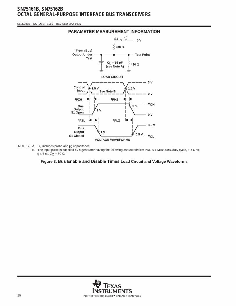
PARAMETER MEASUREMENT INFORMATION
VOLTAGE WAVEFORMS
LOAD CIRCUIT
480 Ω
200 Ω
(see Note A)CL = 30 pF
Test Point
5 V
OutputBus
InputTerminal
See Note B
VOH
VOH
0 V
3 V
tPHL
2.2 V
1.0 V
1.5 V
tPLH
1.5 V
From (Bus)Output Under
Test
NOTES: A. CL includes probe and jig capacitance.B. The input pulse is supplied by a generator having the following characteristics: PRR ≤ 1 MHz, 50% duty cycle, tr ≤ 6 ns,
tf ≤ 6 ns, ZO = 50 Ω.
Figure 1. Terminal-to-Bus Load Circuit and Voltage Waveforms
See Note B1.5 V
tPLH
1.5 V
1.5 V1.5 V
tPHL
3 V
0 V
VOH
VOL
BusInput
Output
From (Terminal)Output Under
Test
4.3 V
Test Point
CL = 30 pF(see Note A)
240 Ω
3 kΩ
LOAD CIRCUIT
VOLTAGE WAVEFORMS
Terminal
NOTES: A. CL includes probe and jig capacitance.B. The input pulse is supplied by a generator having the following characteristics: PRR ≤ 1 MHz, 50% duty cycle, tr ≤ 6 ns,
tf ≤ 6 ns, ZO = 50 Ω.
Figure 2. Bus-to-Terminal Load Circuit and Voltage Waveforms
SN75161B, SN75162BOCTAL GENERAL-PURPOSE INTERFACE BUS TRANSCEIVERS
SLLS005B – OCTOBER 1980 – REVISED MAY 1995
10 POST OFFICE BOX 655303 • DALLAS, TEXAS 75265
PARAMETER MEASUREMENT INFORMATION
NOTES: A. CL includes probe and jig capacitance.B. The input pulse is supplied by a generator having the following characteristics: PRR ≤ 1 MHz, 50% duty cycle, tr ≤ 6 ns,
tf ≤ 6 ns, ZO = 50 Ω.
S1 Open
tPHZ
1.5 V
3 V
0 V
S1 Closed1 V
3.5 V
VOL
InputControl
See Note B1.5 V
tPZH
S1
VOLTAGE WAVEFORMS
2 V
tPZL
90%
0.5 V
tPLZ
VOH
0 V
BusOutput
BusOutput
5 V
Test Point
CL = 15 pF(see Note A)
200 Ω
480 Ω
LOAD CIRCUIT
From (Bus)Output Under
Test
Figure 3. Bus Enable and Disable Times Load Circuit and Voltage Waveforms

SN75161B, SN75162BOCTAL GENERAL-PURPOSE INTERFACE BUS TRANSCEIVERS
SLLS005B – OCTOBER 1980 – REVISED MAY 1995
11POST OFFICE BOX 655303 • DALLAS, TEXAS 75265
PARAMETER MEASUREMENT INFORMATION
90%OutputTerminalS1 Open
S1 Closed
Terminal
tPHZ
VOLTAGE WAVEFORMS
Output
0 V
VOH
tPLZ
0.7 V
tPZL
1.5 V
tPZH
1.5 VSee Note B
ControlInput
VOL
4 V
1 V
0 V
3 V
1.5 V
LOAD CIRCUIT
3 kΩ
240 Ω
Test Point
4.3 VS1
CL = 15 pF(see Note A)
From (Terminal)Output Under
Test
NOTES: A. CL includes probe and jig capacitance.B. The Input pulse is supplied by a generator having the following characteristics: PRR ≤ 1 MHz, 50% duty cycle,
tr ≤ 6 ns, tf ≤ 6 ns, ZO = 50 Ω.
Figure 4. Terminal Enable and Disable Times Load Circuit and Voltage Waveforms
SN75161B, SN75162BOCTAL GENERAL-PURPOSE INTERFACE BUS TRANSCEIVERS
SLLS005B – OCTOBER 1980 – REVISED MAY 1995
12 POST OFFICE BOX 655303 • DALLAS, TEXAS 75265
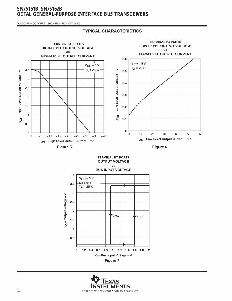
TYPICAL CHARACTERISTICS
VO
H –
Hig
h-Le
vel O
utpu
t Vol
tage
– V
TERMINAL I/O PORTSHIGH-LEVEL OUTPUT VOLTAGE
vsHIGH-LEVEL OUTPUT CURRENT
3.5
3
2.5
2
1.5
1
0.5
–35–30–25–20–15–10–50
–40
4
0
TA = 25°CVCC = 5 V
IOH – High-Level Output Current – mA
V OH
Figure 5
IOL – Low-Level Output Current – mA
VO
L –
Low
-Lev
el O
utpu
t Vol
tage
– V
TERMINAL I/O PORTSLOW-LEVEL OUTPUT VOLTAGE
vsLOW-LEVEL OUTPUT CURRENT
TA = 25°CVCC = 5 V
0.5
0.4
0.3
0.2
0.1
50403020100
60
0.6
0
VO
L
Figure 6
2
VO
– O
utpu
t Vol
tage
– V
TERMINAL I/O PORTSOUTPUT VOLTAGE
vsBUS INPUT VOLTAGE
VIT–
TA = 25°CNo Load
VCC = 5 V
3.5
3
2.5
2
1.5
1
0.5
1.81.61.41.210.80.60.40.20
4
VI – Bus Input Voltage – V
0
V O
VIT+
Figure 7
SN75161B, SN75162BOCTAL GENERAL-PURPOSE INTERFACE BUS TRANSCEIVERS
SLLS005B – OCTOBER 1980 – REVISED MAY 1995
13POST OFFICE BOX 655303 • DALLAS, TEXAS 75265
TYPICAL CHARACTERISTICS
IOH – High-Level Output Current – mA
– H
igh-
Leve
l Out
put V
olta
ge –
V
GPIB I/O PORTSHIGH-LEVEL OUTPUT VOLTAGE
vsHIGH-LEVEL OUTPUT CURRENT
TA = 25°CVCC = 5 V
3
2
1
–50–30–40–20–100
–60
0
0
V OH
Figure 8
IOL – Low-Level Output Current – mA
– L
ow-L
evel
Out
put V
olta
ge –
V
GPIB I/O PORTSLOW-LEVEL OUTPUT VOLTAGE
vsLOW-LEVEL OUTPUT CURRENT
TA = 25°CVCC = 5 V
0.5
0.4
0.3
0.2
0.1
9080706050403020100
100
0.6
0
V OL
Figure 9
Figure 10
VI – Input Voltage – V
VO
– O
utpu
t Vol
tage
– V
GPIB I/O PORTSOUTPUT VOLTAGE
vsTHERMAL INPUT VOLTAGE
TA = 25°CNo LoadVCC = 5 V
3
2
1
1.61.51.41.31.21.110
4
0.9 1.7
VO
– C
urre
nt –
mA
GPIB I/O PORTSCURRENT
vsVOLTAGE
2
1
0
–1
–2
–3
–6
543210–1–7
6
VI/O – Voltage – V
–2
TA = 25°CVCC = 5 V
ÁÁÁÁÁÁÁÁÁÁÁÁÁÁÁÁÁÁÁÁÁÁÁÁ
The UnshadedArea Conforms toParagraph 3.5.3 ofIEEE Standard 488-1978
I I/O
–5
–4
Figure 11
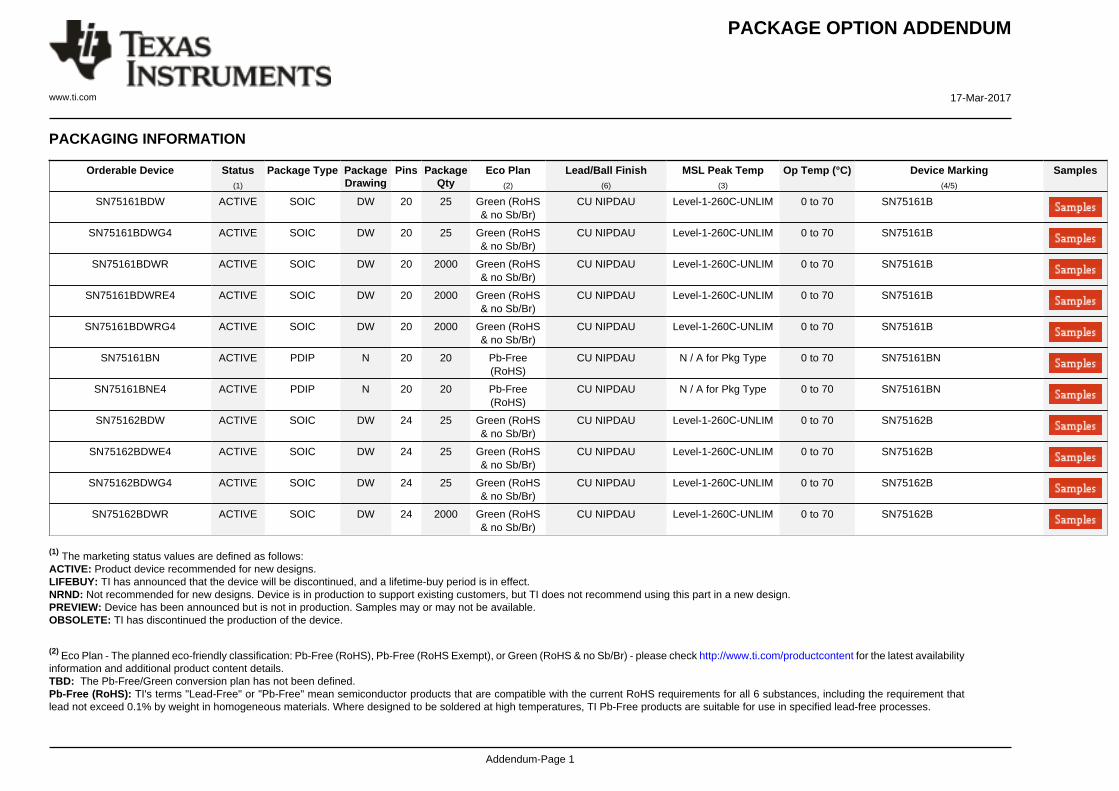
PACKAGE OPTION ADDENDUM
www.ti.com 17-Mar-2017
Addendum-Page 1
PACKAGING INFORMATION
Orderable Device Status(1)
Package Type PackageDrawing
Pins PackageQty
Eco Plan(2)
Lead/Ball Finish(6)
MSL Peak Temp(3)
Op Temp (°C) Device Marking(4/5)
Samples
SN75161BDW ACTIVE SOIC DW 20 25 Green (RoHS& no Sb/Br)
CU NIPDAU Level-1-260C-UNLIM 0 to 70 SN75161B
SN75161BDWG4 ACTIVE SOIC DW 20 25 Green (RoHS& no Sb/Br)
CU NIPDAU Level-1-260C-UNLIM 0 to 70 SN75161B
SN75161BDWR ACTIVE SOIC DW 20 2000 Green (RoHS& no Sb/Br)
CU NIPDAU Level-1-260C-UNLIM 0 to 70 SN75161B
SN75161BDWRE4 ACTIVE SOIC DW 20 2000 Green (RoHS& no Sb/Br)
CU NIPDAU Level-1-260C-UNLIM 0 to 70 SN75161B
SN75161BDWRG4 ACTIVE SOIC DW 20 2000 Green (RoHS& no Sb/Br)
CU NIPDAU Level-1-260C-UNLIM 0 to 70 SN75161B
SN75161BN ACTIVE PDIP N 20 20 Pb-Free(RoHS)
CU NIPDAU N / A for Pkg Type 0 to 70 SN75161BN
SN75161BNE4 ACTIVE PDIP N 20 20 Pb-Free(RoHS)
CU NIPDAU N / A for Pkg Type 0 to 70 SN75161BN
SN75162BDW ACTIVE SOIC DW 24 25 Green (RoHS& no Sb/Br)
CU NIPDAU Level-1-260C-UNLIM 0 to 70 SN75162B
SN75162BDWE4 ACTIVE SOIC DW 24 25 Green (RoHS& no Sb/Br)
CU NIPDAU Level-1-260C-UNLIM 0 to 70 SN75162B
SN75162BDWG4 ACTIVE SOIC DW 24 25 Green (RoHS& no Sb/Br)
CU NIPDAU Level-1-260C-UNLIM 0 to 70 SN75162B
SN75162BDWR ACTIVE SOIC DW 24 2000 Green (RoHS& no Sb/Br)
CU NIPDAU Level-1-260C-UNLIM 0 to 70 SN75162B
(1) The marketing status values are defined as follows:ACTIVE: Product device recommended for new designs.LIFEBUY: TI has announced that the device will be discontinued, and a lifetime-buy period is in effect.NRND: Not recommended for new designs. Device is in production to support existing customers, but TI does not recommend using this part in a new design.PREVIEW: Device has been announced but is not in production. Samples may or may not be available.OBSOLETE: TI has discontinued the production of the device.
(2) Eco Plan - The planned eco-friendly classification: Pb-Free (RoHS), Pb-Free (RoHS Exempt), or Green (RoHS & no Sb/Br) - please check http://www.ti.com/productcontent for the latest availabilityinformation and additional product content details.TBD: The Pb-Free/Green conversion plan has not been defined.Pb-Free (RoHS): TI's terms "Lead-Free" or "Pb-Free" mean semiconductor products that are compatible with the current RoHS requirements for all 6 substances, including the requirement thatlead not exceed 0.1% by weight in homogeneous materials. Where designed to be soldered at high temperatures, TI Pb-Free products are suitable for use in specified lead-free processes.

PACKAGE OPTION ADDENDUM
www.ti.com 17-Mar-2017
Addendum-Page 2
Pb-Free (RoHS Exempt): This component has a RoHS exemption for either 1) lead-based flip-chip solder bumps used between the die and package, or 2) lead-based die adhesive used betweenthe die and leadframe. The component is otherwise considered Pb-Free (RoHS compatible) as defined above.Green (RoHS & no Sb/Br): TI defines "Green" to mean Pb-Free (RoHS compatible), and free of Bromine (Br) and Antimony (Sb) based flame retardants (Br or Sb do not exceed 0.1% by weightin homogeneous material)
(3) MSL, Peak Temp. - The Moisture Sensitivity Level rating according to the JEDEC industry standard classifications, and peak solder temperature.
(4) There may be additional marking, which relates to the logo, the lot trace code information, or the environmental category on the device.
(5) Multiple Device Markings will be inside parentheses. Only one Device Marking contained in parentheses and separated by a "~" will appear on a device. If a line is indented then it is a continuationof the previous line and the two combined represent the entire Device Marking for that device.
(6) Lead/Ball Finish - Orderable Devices may have multiple material finish options. Finish options are separated by a vertical ruled line. Lead/Ball Finish values may wrap to two lines if the finishvalue exceeds the maximum column width.
Important Information and Disclaimer:The information provided on this page represents TI's knowledge and belief as of the date that it is provided. TI bases its knowledge and belief on informationprovided by third parties, and makes no representation or warranty as to the accuracy of such information. Efforts are underway to better integrate information from third parties. TI has taken andcontinues to take reasonable steps to provide representative and accurate information but may not have conducted destructive testing or chemical analysis on incoming materials and chemicals.TI and TI suppliers consider certain information to be proprietary, and thus CAS numbers and other limited information may not be available for release.
In no event shall TI's liability arising out of such information exceed the total purchase price of the TI part(s) at issue in this document sold by TI to Customer on an annual basis.

TAPE AND REEL INFORMATION
*All dimensions are nominal
Device PackageType
PackageDrawing
Pins SPQ ReelDiameter
(mm)
ReelWidth
W1 (mm)
A0(mm)
B0(mm)
K0(mm)
P1(mm)
W(mm)
Pin1Quadrant
SN75161BDWR SOIC DW 20 2000 330.0 24.4 10.8 13.3 2.7 12.0 24.0 Q1
SN75161BDWR SOIC DW 20 2000 330.0 24.4 10.8 13.3 2.7 12.0 24.0 Q1
SN75162BDWR SOIC DW 24 2000 330.0 24.4 10.75 15.7 2.7 12.0 24.0 Q1
PACKAGE MATERIALS INFORMATION
www.ti.com 31-Jan-2014
Pack Materials-Page 1
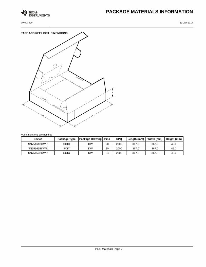
*All dimensions are nominal
Device Package Type Package Drawing Pins SPQ Length (mm) Width (mm) Height (mm)
SN75161BDWR SOIC DW 20 2000 367.0 367.0 45.0
SN75161BDWR SOIC DW 20 2000 367.0 367.0 45.0
SN75162BDWR SOIC DW 24 2000 367.0 367.0 45.0
PACKAGE MATERIALS INFORMATION
www.ti.com 31-Jan-2014
Pack Materials-Page 2


www.ti.com
PACKAGE OUTLINE
C
TYP10.639.97
2.65 MAX
18X 1.27
20X 0.510.31
2X11.43
TYP0.330.10
0 - 80.30.1
0.25GAGE PLANE
1.270.40
A
NOTE 3
13.012.6
B 7.67.4
4220724/A 05/2016
SOIC - 2.65 mm max heightDW0020ASOIC
NOTES: 1. All linear dimensions are in millimeters. Dimensions in parenthesis are for reference only. Dimensioning and tolerancing per ASME Y14.5M. 2. This drawing is subject to change without notice. 3. This dimension does not include mold flash, protrusions, or gate burrs. Mold flash, protrusions, or gate burrs shall not exceed 0.15 mm per side. 4. This dimension does not include interlead flash. Interlead flash shall not exceed 0.43 mm per side.5. Reference JEDEC registration MS-013.
120
0.25 C A B
1110
PIN 1 IDAREA
NOTE 4
SEATING PLANE
0.1 C
SEE DETAIL A
DETAIL ATYPICAL
SCALE 1.200

www.ti.com
EXAMPLE BOARD LAYOUT
(9.3)
0.07 MAXALL AROUND
0.07 MINALL AROUND
20X (2)
20X (0.6)
18X (1.27)
(R )TYP
0.05
4220724/A 05/2016
SOIC - 2.65 mm max heightDW0020ASOIC
SYMM
SYMM
LAND PATTERN EXAMPLESCALE:6X
1
10 11
20
NOTES: (continued) 6. Publication IPC-7351 may have alternate designs. 7. Solder mask tolerances between and around signal pads can vary based on board fabrication site.
METALSOLDER MASKOPENING
NON SOLDER MASKDEFINED
SOLDER MASK DETAILS
SOLDER MASKOPENING
METAL UNDERSOLDER MASK
SOLDER MASKDEFINED
www.ti.com
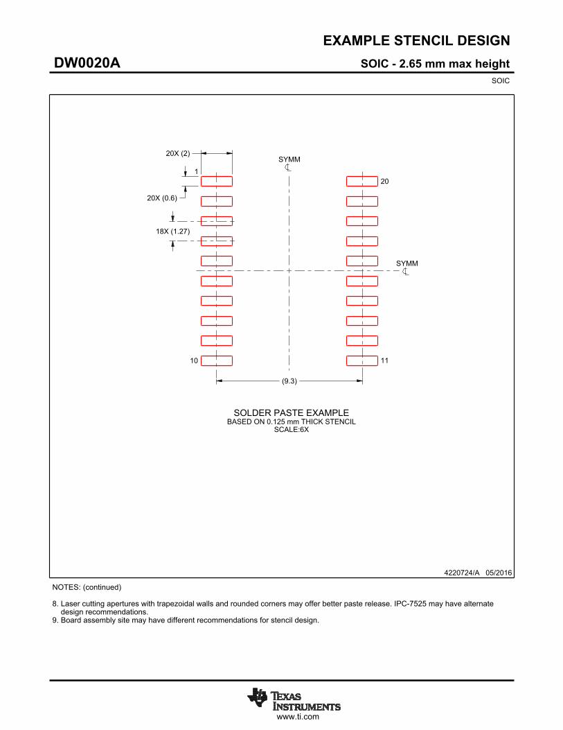
EXAMPLE STENCIL DESIGN
(9.3)
18X (1.27)
20X (0.6)
20X (2)
4220724/A 05/2016
SOIC - 2.65 mm max heightDW0020ASOIC
NOTES: (continued) 8. Laser cutting apertures with trapezoidal walls and rounded corners may offer better paste release. IPC-7525 may have alternate design recommendations. 9. Board assembly site may have different recommendations for stencil design.
SYMM
SYMM
1
10 11
20
SOLDER PASTE EXAMPLEBASED ON 0.125 mm THICK STENCIL
SCALE:6X

IMPORTANT NOTICE
Texas Instruments Incorporated (TI) reserves the right to make corrections, enhancements, improvements and other changes to itssemiconductor products and services per JESD46, latest issue, and to discontinue any product or service per JESD48, latest issue. Buyersshould obtain the latest relevant information before placing orders and should verify that such information is current and complete.TI’s published terms of sale for semiconductor products (http://www.ti.com/sc/docs/stdterms.htm) apply to the sale of packaged integratedcircuit products that TI has qualified and released to market. Additional terms may apply to the use or sale of other types of TI products andservices.Reproduction of significant portions of TI information in TI data sheets is permissible only if reproduction is without alteration and isaccompanied by all associated warranties, conditions, limitations, and notices. TI is not responsible or liable for such reproduceddocumentation. Information of third parties may be subject to additional restrictions. Resale of TI products or services with statementsdifferent from or beyond the parameters stated by TI for that product or service voids all express and any implied warranties for theassociated TI product or service and is an unfair and deceptive business practice. TI is not responsible or liable for any such statements.Buyers and others who are developing systems that incorporate TI products (collectively, “Designers”) understand and agree that Designersremain responsible for using their independent analysis, evaluation and judgment in designing their applications and that Designers havefull and exclusive responsibility to assure the safety of Designers' applications and compliance of their applications (and of all TI productsused in or for Designers’ applications) with all applicable regulations, laws and other applicable requirements. Designer represents that, withrespect to their applications, Designer has all the necessary expertise to create and implement safeguards that (1) anticipate dangerousconsequences of failures, (2) monitor failures and their consequences, and (3) lessen the likelihood of failures that might cause harm andtake appropriate actions. Designer agrees that prior to using or distributing any applications that include TI products, Designer willthoroughly test such applications and the functionality of such TI products as used in such applications.TI’s provision of technical, application or other design advice, quality characterization, reliability data or other services or information,including, but not limited to, reference designs and materials relating to evaluation modules, (collectively, “TI Resources”) are intended toassist designers who are developing applications that incorporate TI products; by downloading, accessing or using TI Resources in anyway, Designer (individually or, if Designer is acting on behalf of a company, Designer’s company) agrees to use any particular TI Resourcesolely for this purpose and subject to the terms of this Notice.TI’s provision of TI Resources does not expand or otherwise alter TI’s applicable published warranties or warranty disclaimers for TIproducts, and no additional obligations or liabilities arise from TI providing such TI Resources. TI reserves the right to make corrections,enhancements, improvements and other changes to its TI Resources. TI has not conducted any testing other than that specificallydescribed in the published documentation for a particular TI Resource.Designer is authorized to use, copy and modify any individual TI Resource only in connection with the development of applications thatinclude the TI product(s) identified in such TI Resource. NO OTHER LICENSE, EXPRESS OR IMPLIED, BY ESTOPPEL OR OTHERWISETO ANY OTHER TI INTELLECTUAL PROPERTY RIGHT, AND NO LICENSE TO ANY TECHNOLOGY OR INTELLECTUAL PROPERTYRIGHT OF TI OR ANY THIRD PARTY IS GRANTED HEREIN, including but not limited to any patent right, copyright, mask work right, orother intellectual property right relating to any combination, machine, or process in which TI products or services are used. Informationregarding or referencing third-party products or services does not constitute a license to use such products or services, or a warranty orendorsement thereof. Use of TI Resources may require a license from a third party under the patents or other intellectual property of thethird party, or a license from TI under the patents or other intellectual property of TI.TI RESOURCES ARE PROVIDED “AS IS” AND WITH ALL FAULTS. TI DISCLAIMS ALL OTHER WARRANTIES ORREPRESENTATIONS, EXPRESS OR IMPLIED, REGARDING RESOURCES OR USE THEREOF, INCLUDING BUT NOT LIMITED TOACCURACY OR COMPLETENESS, TITLE, ANY EPIDEMIC FAILURE WARRANTY AND ANY IMPLIED WARRANTIES OFMERCHANTABILITY, FITNESS FOR A PARTICULAR PURPOSE, AND NON-INFRINGEMENT OF ANY THIRD PARTY INTELLECTUALPROPERTY RIGHTS. TI SHALL NOT BE LIABLE FOR AND SHALL NOT DEFEND OR INDEMNIFY DESIGNER AGAINST ANY CLAIM,INCLUDING BUT NOT LIMITED TO ANY INFRINGEMENT CLAIM THAT RELATES TO OR IS BASED ON ANY COMBINATION OFPRODUCTS EVEN IF DESCRIBED IN TI RESOURCES OR OTHERWISE. IN NO EVENT SHALL TI BE LIABLE FOR ANY ACTUAL,DIRECT, SPECIAL, COLLATERAL, INDIRECT, PUNITIVE, INCIDENTAL, CONSEQUENTIAL OR EXEMPLARY DAMAGES INCONNECTION WITH OR ARISING OUT OF TI RESOURCES OR USE THEREOF, AND REGARDLESS OF WHETHER TI HAS BEENADVISED OF THE POSSIBILITY OF SUCH DAMAGES.Unless TI has explicitly designated an individual product as meeting the requirements of a particular industry standard (e.g., ISO/TS 16949and ISO 26262), TI is not responsible for any failure to meet such industry standard requirements.Where TI specifically promotes products as facilitating functional safety or as compliant with industry functional safety standards, suchproducts are intended to help enable customers to design and create their own applications that meet applicable functional safety standardsand requirements. Using products in an application does not by itself establish any safety features in the application. Designers mustensure compliance with safety-related requirements and standards applicable to their applications. Designer may not use any TI products inlife-critical medical equipment unless authorized officers of the parties have executed a special contract specifically governing such use.Life-critical medical equipment is medical equipment where failure of such equipment would cause serious bodily injury or death (e.g., lifesupport, pacemakers, defibrillators, heart pumps, neurostimulators, and implantables). Such equipment includes, without limitation, allmedical devices identified by the U.S. Food and Drug Administration as Class III devices and equivalent classifications outside the U.S.TI may expressly designate certain products as completing a particular qualification (e.g., Q100, Military Grade, or Enhanced Product).Designers agree that it has the necessary expertise to select the product with the appropriate qualification designation for their applicationsand that proper product selection is at Designers’ own risk. Designers are solely responsible for compliance with all legal and regulatoryrequirements in connection with such selection.Designer will fully indemnify TI and its representatives against any damages, costs, losses, and/or liabilities arising out of Designer’s non-compliance with the terms and provisions of this Notice.
Mailing Address: Texas Instruments, Post Office Box 655303, Dallas, Texas 75265Copyright © 2017, Texas Instruments Incorporated