Embed Size (px)
Citation preview
SmartFusion2 MSSCreating a Design Using MSS Fabric Interfaces
SmartFusion2 MSS Creating a Design Using MSS Fabric Interfaces
2
Table of Contents
Introduction . . . . . . . . . . . . . . . . . . . . . . . . . . . . . . . . . . . . . . . . . . . . . . . . . . . . . . . . . . . . . . . . . . . . . . 3High-Level View . . . . . . . . . . . . . . . . . . . . . . . . . . . . . . . . . . . . . . . . . . . . . . . . . . . . . . . . . . . . . . . . . . . . . . . . . . . . 3
1 MSS Configurator. . . . . . . . . . . . . . . . . . . . . . . . . . . . . . . . . . . . . . . . . . . . . . . . . . . . . . . . . . . . . . . . . . 6
2 SmartDesign and MSS Configurator Actions . . . . . . . . . . . . . . . . . . . . . . . . . . . . . . . . . . . . . . . . . . . . . 7
3 Configuring the DDR_FIC Sub-System . . . . . . . . . . . . . . . . . . . . . . . . . . . . . . . . . . . . . . . . . . . . . . . . . 8Step 1: Configure the MSS MDDR Sub-block to Expose the DDR_FIC Bus Interface . . . . . . . . . . . . . . . . . . . . . . 8
Step 2: Create the FPGA Fabric DDR_FIC Sub-System . . . . . . . . . . . . . . . . . . . . . . . . . . . . . . . . . . . . . . . . . . . . . 9
4 Configuring the SMC_FIC Sub-System . . . . . . . . . . . . . . . . . . . . . . . . . . . . . . . . . . . . . . . . . . . . . . . . 13Step 1: Configure the MSS MDDR Sub-block to Expose the SMC_FIC Bus Interface . . . . . . . . . . . . . . . . . . . . . 13
Step 2: Create the FPGA Fabric SMC_FIC Sub-System . . . . . . . . . . . . . . . . . . . . . . . . . . . . . . . . . . . . . . . . . . . . 15
5 Configuring the FIC Sub-Systems . . . . . . . . . . . . . . . . . . . . . . . . . . . . . . . . . . . . . . . . . . . . . . . . . . . . 17Step 1: Configure the MSS FIC Sub-Block . . . . . . . . . . . . . . . . . . . . . . . . . . . . . . . . . . . . . . . . . . . . . . . . . . . . . . 17
Step 2: Create the FPGA Fabric FIC Sub-System . . . . . . . . . . . . . . . . . . . . . . . . . . . . . . . . . . . . . . . . . . . . . . . . . 18
6 Configuring the FIC Sub-System Clocks . . . . . . . . . . . . . . . . . . . . . . . . . . . . . . . . . . . . . . . . . . . . . . . 23Step 1: Configure the MSS CCC Sub-Block . . . . . . . . . . . . . . . . . . . . . . . . . . . . . . . . . . . . . . . . . . . . . . . . . . . . . 24
Step 2: Configure the FPGA Fabric FIC clocks . . . . . . . . . . . . . . . . . . . . . . . . . . . . . . . . . . . . . . . . . . . . . . . . . . . 24
Step 3: Connect the FPGA Fabric FIC Sub-Systems Clock Networks . . . . . . . . . . . . . . . . . . . . . . . . . . . . . . . . . 25
Step 4: Connect the MSS CLK_BASE Port . . . . . . . . . . . . . . . . . . . . . . . . . . . . . . . . . . . . . . . . . . . . . . . . . . . . . . 25
Step 5: Connect the MSS MCCC_CLK_BASE_PLL_LOCK Port . . . . . . . . . . . . . . . . . . . . . . . . . . . . . . . . . . . . . 25
Timing Analysis Requirements . . . . . . . . . . . . . . . . . . . . . . . . . . . . . . . . . . . . . . . . . . . . . . . . . . . . . . . . . . . . . . . 26
7 Configuring the FIC Sub-System Reset . . . . . . . . . . . . . . . . . . . . . . . . . . . . . . . . . . . . . . . . . . . . . . . . 27
8 Configuring the System Memory Map . . . . . . . . . . . . . . . . . . . . . . . . . . . . . . . . . . . . . . . . . . . . . . . . . 28Configuring the Memory Map (Generic SmartDesign Behavior) . . . . . . . . . . . . . . . . . . . . . . . . . . . . . . . . . . . . . . 28
Configuring the Memory Regions for the FIC Interfaces (MSS Master View) . . . . . . . . . . . . . . . . . . . . . . . . . . . . 29
Memory Map Computation General Formula . . . . . . . . . . . . . . . . . . . . . . . . . . . . . . . . . . . . . . . . . . . . . . . . . . . . . 30
A Product Support . . . . . . . . . . . . . . . . . . . . . . . . . . . . . . . . . . . . . . . . . . . . . . . . . . . . . . . . . . . . . . . . . . 31Customer Service . . . . . . . . . . . . . . . . . . . . . . . . . . . . . . . . . . . . . . . . . . . . . . . . . . . . . . . . . . . . . . . . . . . . . . . . . 31
Customer Technical Support Center . . . . . . . . . . . . . . . . . . . . . . . . . . . . . . . . . . . . . . . . . . . . . . . . . . . . . . . . . . . 31
Technical Support . . . . . . . . . . . . . . . . . . . . . . . . . . . . . . . . . . . . . . . . . . . . . . . . . . . . . . . . . . . . . . . . . . . . . . . . . 31
Website . . . . . . . . . . . . . . . . . . . . . . . . . . . . . . . . . . . . . . . . . . . . . . . . . . . . . . . . . . . . . . . . . . . . . . . . . . . . . . . . . 31
Contacting the Customer Technical Support Center . . . . . . . . . . . . . . . . . . . . . . . . . . . . . . . . . . . . . . . . . . . . . . . 31
ITAR Technical Support . . . . . . . . . . . . . . . . . . . . . . . . . . . . . . . . . . . . . . . . . . . . . . . . . . . . . . . . . . . . . . . . . . . . . 32
Introduction
The SmartFusion2 Microcontroller Sub-System (MSS) offers four different Fabric Interface Controllers (FIC):
• DDR_FIC
• SMC_FIC
• FIC_0 and FIC_1, depending on your device
These interface blocks enable the MSS to interface with logic implemented in the FPGA fabric and vice versa.
The DDR_FIC is used when you configure the MSS DDR block (MDDR) such that the external DDR memory can be accessed from an FPGA fabric master via an AXI interface or 2 AHBLite AMBA interfaces.
The SMC_FIC is used when you configure the MSS DDR Block in the Single Date Rate (SDR) mode. In this configuration, the MSS accesses external Single Data Rate DRAM or Asynchronous memories via a soft memory controller instantiated in the FPGA fabric, such as CoreSDR_AXI. The SMC_FIC is an AXI or AHBLite slave AMBA interface. The DDR_FIC and SMC_FIC interfaces are mutually exclusive; only one is active at a time.
The FIC interfaces enable you to naturally extend the MSS AMBA Bus into the FPGA fabric. There are up to two FIC instances per MSS depending on the selected device. The first instance is named FIC_0 (which is available on every device) and the second is named FIC_1 (may not be present in the smaller devices). You can configure the FIC as either an APB3 or AHBLite AMBA interface depending on your design needs. In each mode, a master and a slave bus interface is available. That is, a master in the fabric can interface to a slave in the MSS and a master in the MSS can interface to a slave in the fabric.
Each Fabric Interface sub-system can operate on a different clock frequency, defined as a ratio of the MSS main clock M3_CLK.
The SmartFusion2 architecture imposes rules related to clocking domains between the Fabric Interfaces and the FPGA Fabric. This document provides guidance on how to properly construct such systems.
High-Level ViewFigure 1 and Figure 2 show how the MSS connects to the FPGA fabric via the various Fabric Interface Controllers (FIC). Figure 1 shows an overall block diagram when DDR_FIC is used (external DDR memory) and Figure 2 shows a block diagram for when SMC_FIC is used (external SDR memory).
The diagrams show the MSS sub-blocks essential to connecting the MSS to the FPGA fabric. The FIC sub-block may or not be used in your application. You also may not be using the DDR_FIC or SMC_FIC
3
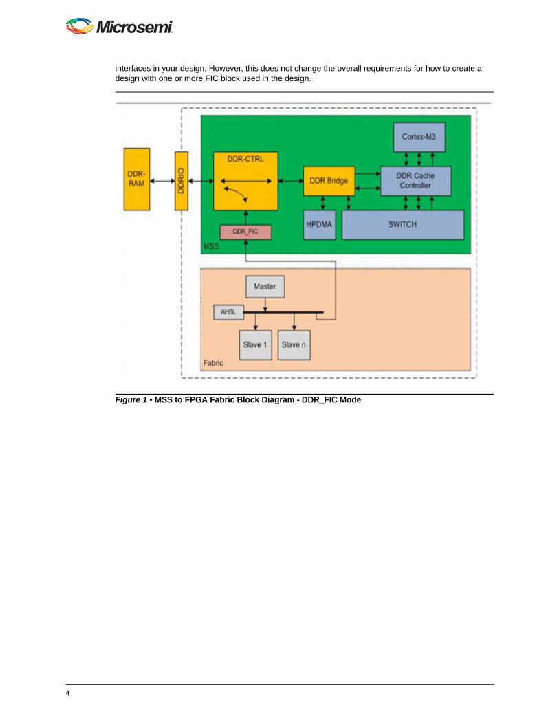
interfaces in your design. However, this does not change the overall requirements for how to create a design with one or more FIC block used in the design.
Figure 1 • MSS to FPGA Fabric Block Diagram - DDR_FIC Mode
4
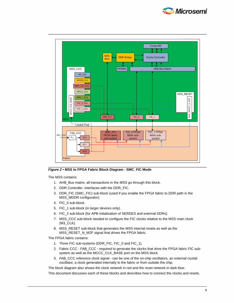
The MSS contains:
1. AHB_Bus matrix; all transactions in the MSS go through this block.
2. DDR Controller -interfaces with the DDR_FIC.
3. DDR_FIC (SMC_FIC) sub-block (used if you enable the FPGA fabric to DDR path in the MSS_MDDR configurator).
4. FIC_0 sub-block.
5. FIC_1 sub-block (in larger devices only).
6. FIC_2 sub-block (for APB initialization of SERDES and external DDRs).
7. MSS_CCC sub-block needed to configure the FIC clocks relative to the MSS main clock (M3_CLK).
8. MSS_RESET sub-block that generates the MSS internal resets as well as the MSS_RESET_N_M2F signal that drives the FPGA fabric.
The FPGA fabric contains:
1. Three FIC sub-systems (DDR_FIC, FIC_0 and FIC_1).
2. Fabric CCC - FAB_CCC - required to generate the clocks that drive the FPGA fabric FIC sub-system as well as the MCCC_CLK_BASE port on the MSS block.
3. FAB_CCC reference clock signal - can be one of the on-chip oscillators, an external crystal oscillator, a clock generated internally to the fabric or from outside the chip.
The block diagram also shows the clock network in red and the reset network in dark blue.
This document discusses each of these blocks and describes how to connect the clocks and resets.
Figure 2 • MSS to FPGA Fabric Block Diagram - SMC_FIC Mode
5
6
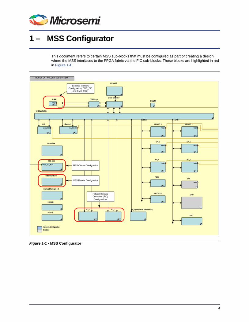
1 – MSS Configurator
This document refers to certain MSS sub-blocks that must be configured as part of creating a design where the MSS interfaces to the FPGA fabric via the FIC sub-blocks. Those blocks are highlighted in red in Figure 1-1.
Figure 1-1 • MSS Configurator
7
2 – SmartDesign and MSS Configurator Actions
There are several common actions referenced in this document; they are summarized in the following list:. If you are familiar with SmartDesign and the MSS you can skip to the next section.
Instantiating a core - The action of selecting a core from the Libero SoC IP catalog, dragging and dropping that core onto a SmartDesign Canvas.
Configuring a core - The action of opening the configurator for an instance of that core on the Canvas, selecting a particular configuration and committing it by clicking OK in the configurator dialog box. As a result of that action, only ports pertinent to the current configuration are visible and available for use.
Instantiating a component - The action of selecting a component in the Libero SoC Design Hierarchy, dragging and dropping that component onto a SmartDesign canvas.
Instantiating a custom AMBA compliant component - The action of selecting an HDL+ component in the Libero SoC Design Hierarchy, dragging and dropping that component onto a SmartDesign Canvas. Using the HDL+ feature enables you to add AMBA compliant Bus Interfaces (BIFs) to your regular HDL module.
Configuring a component - The action of opening the configurator for a component instantiated on a SmartDesign Canvas or from the Design Hierarchy, selecting a particular configuration and committing it by clicking OK in the configurator dialog box. As a result of that action, all instances on that component in the Libero SoC project are affected and need to be updated. When an instance is updated with the latest component, only ports pertinent to the current configuration are visible and available for use.
Enabling an MSS sub-block - Some MSS sub-blocks can be enabled or disabled, indicating that they are used in the current application. All unused sub-blocks should be disabled.
Configuring an MSS sub-block - The action of opening the configurator for that sub-block in the MSS configurator, selecting a particular configuration and committing it by clicking OK in the configurator dialog box, then saving the MSS configuration. As the result of these actions, the MSS component has a new configuration and potentially a new port interface. When the instance of the MSS is updated with the latest component, only the MSS ports pertinent to the current configuration are visible and available for use.
Creating a FPGA fabric sub-system - The action of instantiating, configuring cores and components in a SmartDesign Canvas and connecting them together and to the MSS component instantiated already in that particular SmartDesign.
3 – Configuring the DDR_FIC Sub-System
To configure/create a DDR_FIC sub-system, you must:
1. Configure the MSS MDDR to expose the DDR_FIC interface
2. Create the FPGA fabric DDR_FIC sub-system including instantiation/configuration/connectivity for:
– AXI or AHBLite bus
– AXI or AHBLite bus master(s)
– Other masters and peripherals on the bus as required by your application
– Clocks and resets; refer to "Configuring the FIC Sub-System Clocks" on page 23 and "Configuring the FIC Sub-System Reset" on page 27
These steps are described in detail below.
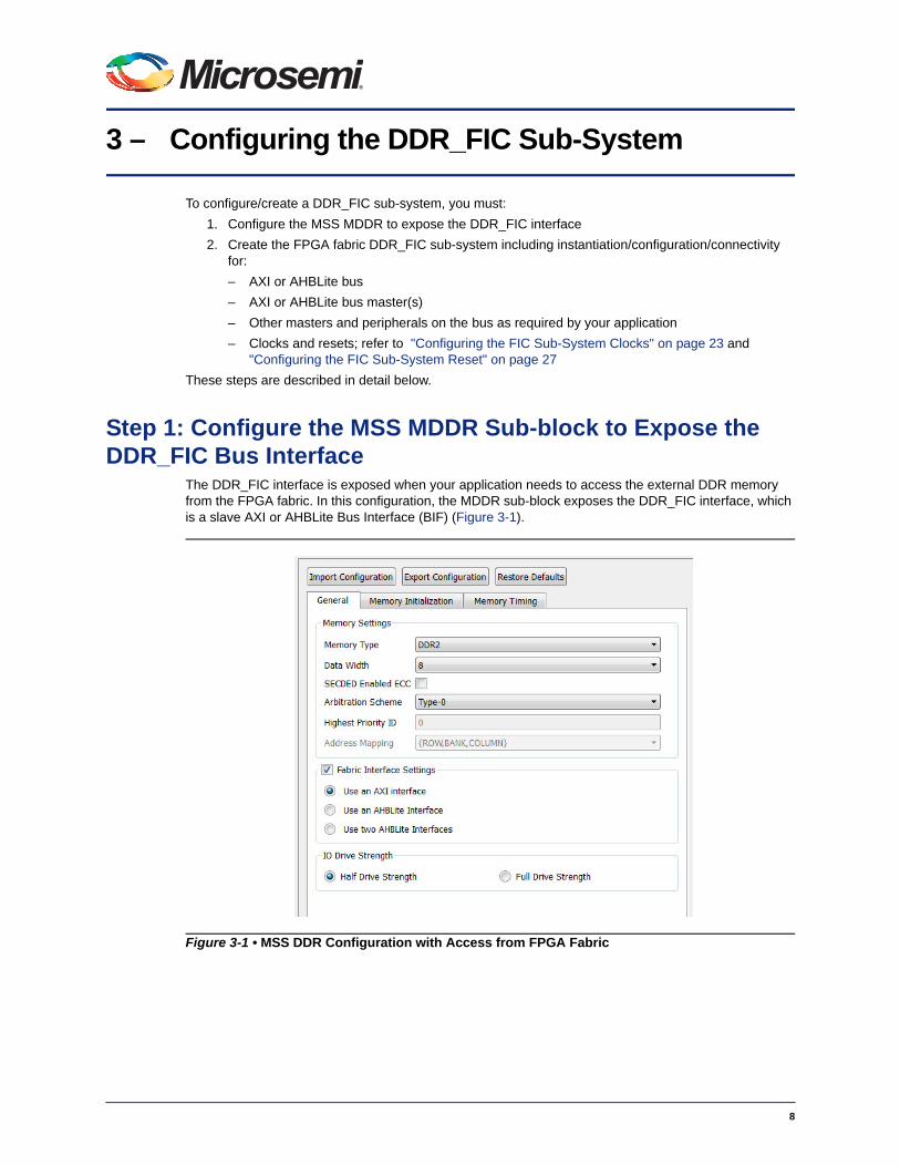
Step 1: Configure the MSS MDDR Sub-block to Expose the DDR_FIC Bus Interface
The DDR_FIC interface is exposed when your application needs to access the external DDR memory from the FPGA fabric. In this configuration, the MDDR sub-block exposes the DDR_FIC interface, which is a slave AXI or AHBLite Bus Interface (BIF) (Figure 3-1).
Figure 3-1 • MSS DDR Configuration with Access from FPGA Fabric
8
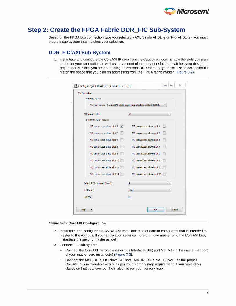
Step 2: Create the FPGA Fabric DDR_FIC Sub-SystemBased on the FPGA bus connection type you selected - AXI, Single AHBLite or Two AHBLite - you must create a sub-system that matches your selection.
DDR_FIC/AXI Sub-System1. Instantiate and configure the CoreAXI IP core from the Catalog window. Enable the slots you plan
to use for your application as well as the amount of memory per slot that matches your design requirements. Since you are addressing an external DDR memory, your slot size selection should match the space that you plan on addressing from the FPGA fabric master. (Figure 3-2).
2. Instantiate and configure the AMBA AXI-compliant master core or component that is intended to master to the AXI bus. If your application requires more than one master onto the CoreAXI bus, instantiate the second master as well.
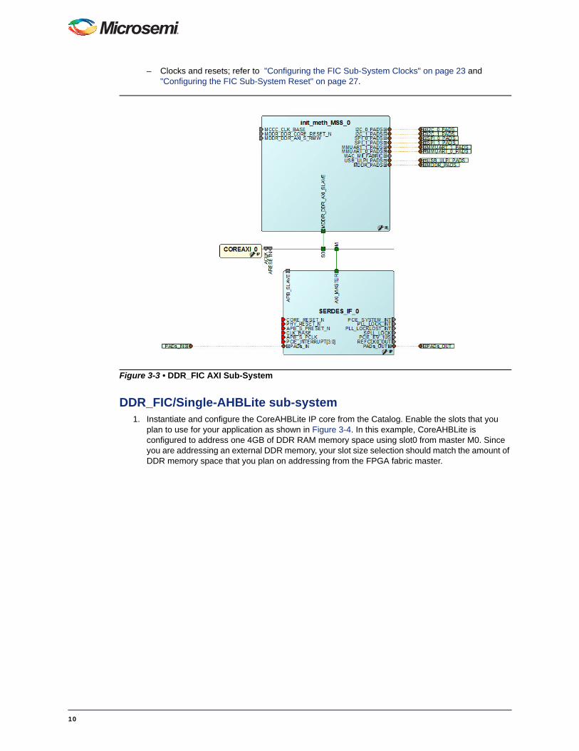
3. Connect the sub-system:
– Connect the CoreAXI mirrored-master Bus Interface (BIF) port M0 (M1) to the master BIF port of your master core instance(s) (Figure 3-3).
– Connect the MSS DDR_FIC slave BIF port - MDDR_DDR_AXI_SLAVE - to the proper CoreAXI bus mirrored-slave slot as per your memory map requirement. If you have other slaves on that bus, connect them also, as per you memory map.
Figure 3-2 • CoreAXI Configuration
9
– Clocks and resets; refer to "Configuring the FIC Sub-System Clocks" on page 23 and "Configuring the FIC Sub-System Reset" on page 27.
DDR_FIC/Single-AHBLite sub-system1. Instantiate and configure the CoreAHBLite IP core from the Catalog. Enable the slots that you
plan to use for your application as shown in Figure 3-4. In this example, CoreAHBLite is configured to address one 4GB of DDR RAM memory space using slot0 from master M0. Since you are addressing an external DDR memory, your slot size selection should match the amount of DDR memory space that you plan on addressing from the FPGA fabric master.
Figure 3-3 • DDR_FIC AXI Sub-System
10
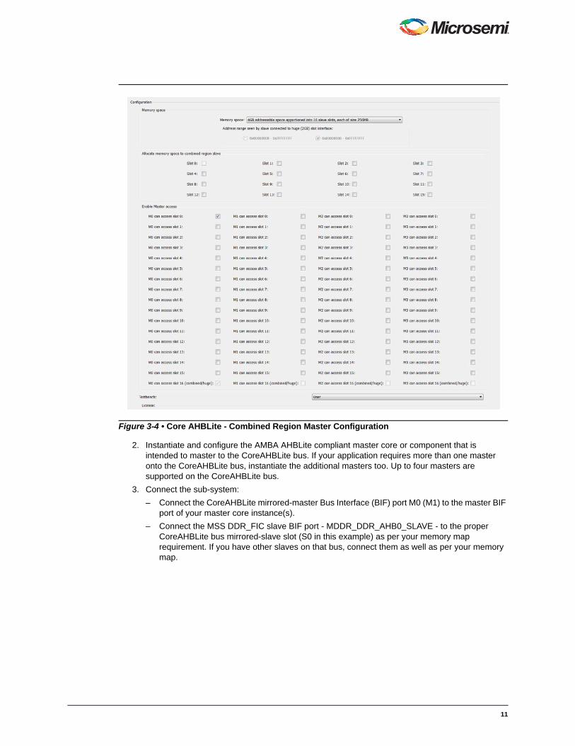
2. Instantiate and configure the AMBA AHBLite compliant master core or component that is intended to master to the CoreAHBLite bus. If your application requires more than one master onto the CoreAHBLite bus, instantiate the additional masters too. Up to four masters are supported on the CoreAHBLite bus.
3. Connect the sub-system:
– Connect the CoreAHBLite mirrored-master Bus Interface (BIF) port M0 (M1) to the master BIF port of your master core instance(s).
– Connect the MSS DDR_FIC slave BIF port - MDDR_DDR_AHB0_SLAVE - to the proper CoreAHBLite bus mirrored-slave slot (S0 in this example) as per your memory map requirement. If you have other slaves on that bus, connect them as well as per your memory map.
Figure 3-4 • Core AHBLite - Combined Region Master Configuration
11
– Clocks and resets; refer to "Configuring the FIC Sub-System Clocks" on page 23 and "Configuring the FIC Sub-System Reset" on page 27.
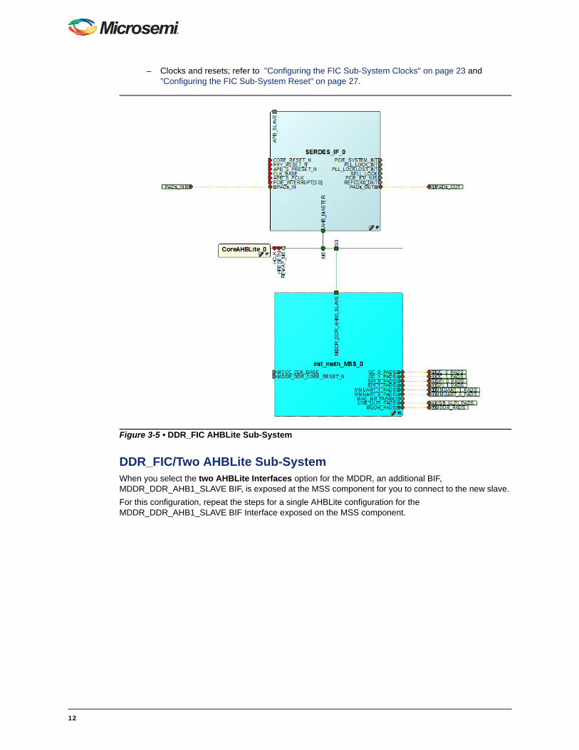
DDR_FIC/Two AHBLite Sub-SystemWhen you select the two AHBLite Interfaces option for the MDDR, an additional BIF, MDDR_DDR_AHB1_SLAVE BIF, is exposed at the MSS component for you to connect to the new slave.
For this configuration, repeat the steps for a single AHBLite configuration for the MDDR_DDR_AHB1_SLAVE BIF Interface exposed on the MSS component.
Figure 3-5 • DDR_FIC AHBLite Sub-System
12
4 – Configuring the SMC_FIC Sub-System
Although the SMC_FIC can be used as an AXI or AHBLite bus interface, this document only describes how to use the SMC_FIC interface configured in AXI mode to connect to the CoreSDR_AXI core. That core is an AXI-based SDR RAM controller used to connect, in this case, the MSS to an external Single Data Rate (SDR) memory component. You can easily infer how to use the AHBLite interface from the following description; the steps are very similar. The AXI interface is a more efficient interface and is the preferred option.
To configure/create a SMC_FIC sub-system, you must:
1. Configure the MSS MDDR to expose the SMC_FIC interface
2. Create the FPGA fabric DDR_FIC sub-system, including instantiation/configuration/connectivity for:
– CoreAXI bus
– CoreSDR_AXI
– Other masters and peripherals on the bus as required by your application
– Clocks and resets; refer to "Configuring the FIC Sub-System Clocks" on page 23 and "Configuring the FIC Sub-System Reset" on page 27
These steps are described in detail below.
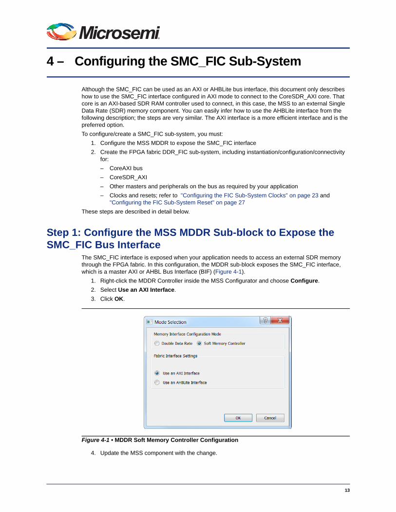
Step 1: Configure the MSS MDDR Sub-block to Expose the SMC_FIC Bus Interface
The SMC_FIC interface is exposed when your application needs to access an external SDR memory through the FPGA fabric. In this configuration, the MDDR sub-block exposes the SMC_FIC interface, which is a master AXI or AHBL Bus Interface (BIF) (Figure 4-1).
1. Right-click the MDDR Controller inside the MSS Configurator and choose Configure.
2. Select Use an AXI Interface.
3. Click OK.
4. Update the MSS component with the change.
Figure 4-1 • MDDR Soft Memory Controller Configuration
13

(Right-click the MSS Component and choose Update Instances with Latest Component). The MDDR_SMC_AXI_MASTER is exposed as a Bus Interface Port of the MSS component.
14
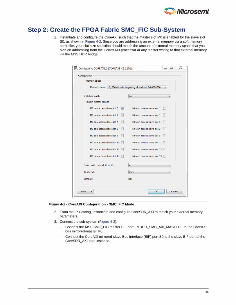
Step 2: Create the FPGA Fabric SMC_FIC Sub-System1. Instantiate and configure the CoreAXI such that the master slot M0 is enabled for the slave slot
S0, as shown in Figure 4-2. Since you are addressing an external memory via a soft memory controller, your slot size selection should match the amount of external memory space that you plan on addressing from the Cortex-M3 processor or any master writing to that external memory via the MSS DDR bridge.
2. From the IP Catalog, instantiate and configure CoreSDR_AXI to match your external memory parameters.
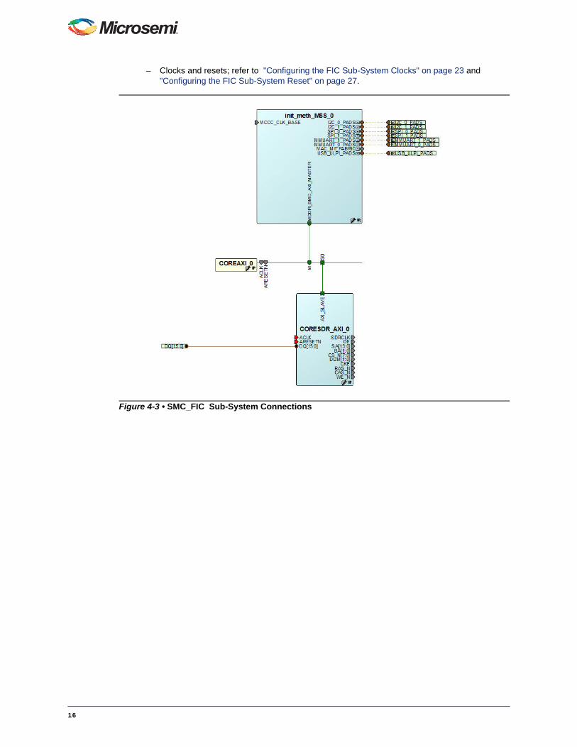
3. Connect the sub-system (Figure 4-3):
– Connect the MSS SMC_FIC master BIF port - MDDR_SMC_AXI_MASTER - to the CoreAXI bus mirrored-master M0.
– Connect the CoreAXI mirrored-slave Bus Interface (BIF) port S0 to the slave BIF port of the CoreSDR_AXI core instance.
Figure 4-2 • CoreAXI Configuration - SMC_FIC Mode
15
– Clocks and resets; refer to "Configuring the FIC Sub-System Clocks" on page 23 and "Configuring the FIC Sub-System Reset" on page 27.
Figure 4-3 • SMC_FIC Sub-System Connections
16
5 – Configuring the FIC Sub-Systems
To configure/create a FIC sub-system, you must:
1. Configure the MSS FIC to expose the FIC interface
2. Create the FPGA fabric FIC sub-system including instantiation/configuration/connectivity for:
– APB3 or AHBLite bus
– APB3 and AHBLite compliant master and/or peripherals configuration and connection onto the bus as required by your application
– Clocks and resets; refer to "Configuring the FIC Sub-System Clocks" on page 23 and "Configuring the FIC Sub-System Reset" on page 27
These steps are described in detail below.
Step 1: Configure the MSS FIC Sub-Block1. Invoke the FIC Configurator and right-click on FIC_0 or FIC_1 to open the FIC Configurator.
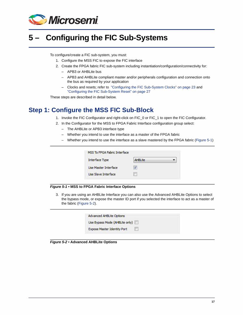
2. In the Configurator for the MSS to FPGA Fabric Interface configuration group select:
– The AHBLite or APB3 interface type
– Whether you intend to use the interface as a master of the FPGA fabric
– Whether you intend to use the interface as a slave mastered by the FPGA fabric (Figure 5-1)
3. If you are using an AHBLite Interface you can also use the Advanced AHBLite Options to select the bypass mode, or expose the master ID port if you selected the interface to act as a master of the fabric (Figure 5-2).
Figure 5-1 • MSS to FPGA Fabric Interface Options
Figure 5-2 • Advanced AHBLite Options
17
Step 2: Create the FPGA Fabric FIC Sub-SystemFor each FIC interface exposed - master and slave, you must instantiate a bus (CoreAHBLite or CoreAPB3) that matches the type you selected. Depending on the interface role (master/slave) and type (AHBLite/APB3), the bus must be configured as follows:
Master/AHBLiteInstantiate and configure the CoreAHBLite bus as follows:
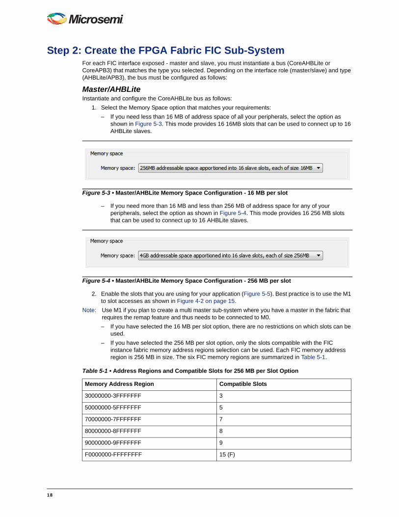
1. Select the Memory Space option that matches your requirements:
– If you need less than 16 MB of address space of all your peripherals, select the option as shown in Figure 5-3. This mode provides 16 16MB slots that can be used to connect up to 16 AHBLite slaves.
– If you need more than 16 MB and less than 256 MB of address space for any of your peripherals, select the option as shown in Figure 5-4. This mode provides 16 256 MB slots that can be used to connect up to 16 AHBLite slaves.
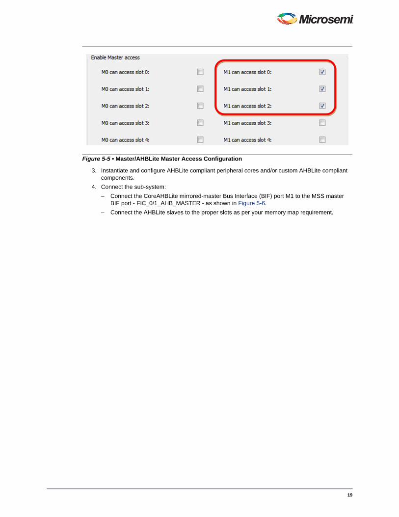
2. Enable the slots that you are using for your application (Figure 5-5). Best practice is to use the M1 to slot accesses as shown in Figure 4-2 on page 15.
Note: Use M1 if you plan to create a multi master sub-system where you have a master in the fabric that requires the remap feature and thus needs to be connected to M0.
– If you have selected the 16 MB per slot option, there are no restrictions on which slots can be used.
– If you have selected the 256 MB per slot option, only the slots compatible with the FIC instance fabric memory address regions selection can be used. Each FIC memory address region is 256 MB in size. The six FIC memory regions are summarized in Table 5-1.
Figure 5-3 • Master/AHBLite Memory Space Configuration - 16 MB per slot
Figure 5-4 • Master/AHBLite Memory Space Configuration - 256 MB per slot
Table 5-1 • Address Regions and Compatible Slots for 256 MB per Slot Option
Memory Address Region Compatible Slots
30000000-3FFFFFFF 3
50000000-5FFFFFFF 5
70000000-7FFFFFFF 7
80000000-8FFFFFFF 8
90000000-9FFFFFFF 9
F0000000-FFFFFFFF 15 (F)
18
3. Instantiate and configure AHBLite compliant peripheral cores and/or custom AHBLite compliant components.
4. Connect the sub-system:
– Connect the CoreAHBLite mirrored-master Bus Interface (BIF) port M1 to the MSS master BIF port - FIC_0/1_AHB_MASTER - as shown in Figure 5-6.
– Connect the AHBLite slaves to the proper slots as per your memory map requirement.
Figure 5-5 • Master/AHBLite Master Access Configuration
19
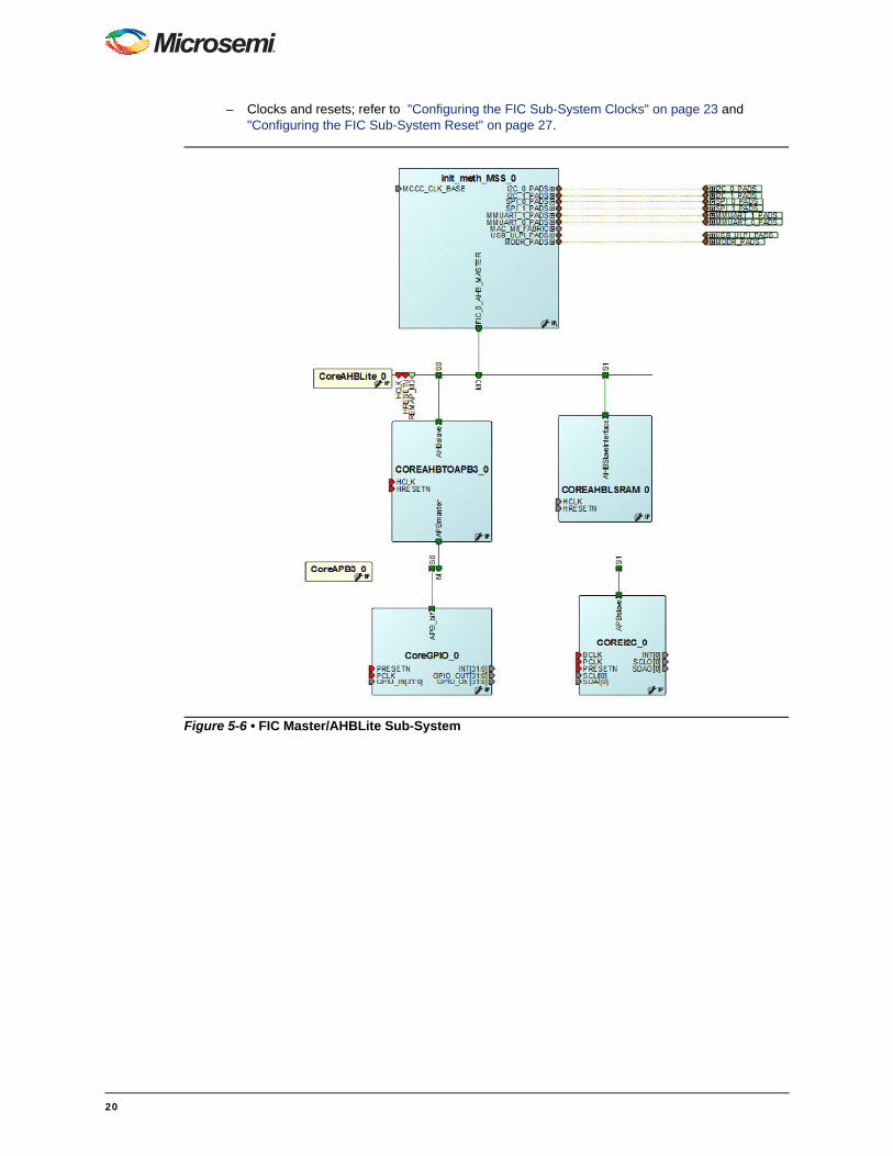
– Clocks and resets; refer to "Configuring the FIC Sub-System Clocks" on page 23 and "Configuring the FIC Sub-System Reset" on page 27.
Figure 5-6 • FIC Master/AHBLite Sub-System
20
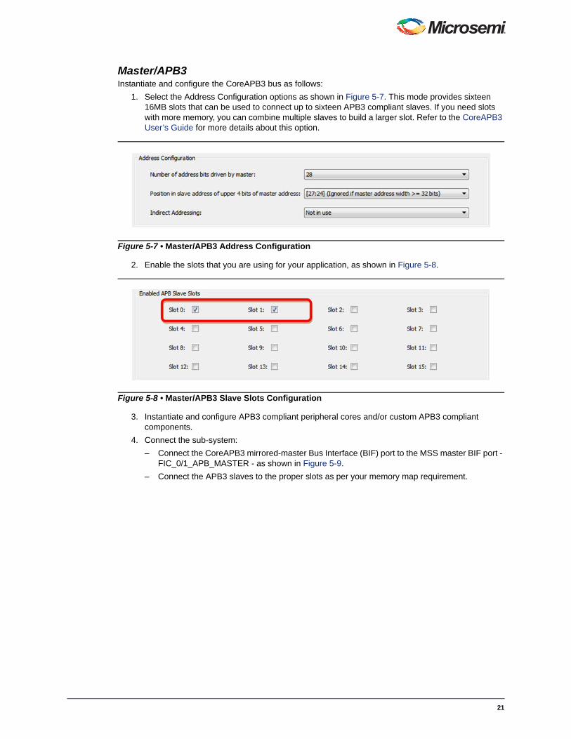
Master/APB3Instantiate and configure the CoreAPB3 bus as follows:
1. Select the Address Configuration options as shown in Figure 5-7. This mode provides sixteen 16MB slots that can be used to connect up to sixteen APB3 compliant slaves. If you need slots with more memory, you can combine multiple slaves to build a larger slot. Refer to the CoreAPB3 User’s Guide for more details about this option.
2. Enable the slots that you are using for your application, as shown in Figure 5-8.
3. Instantiate and configure APB3 compliant peripheral cores and/or custom APB3 compliant components.
4. Connect the sub-system:
– Connect the CoreAPB3 mirrored-master Bus Interface (BIF) port to the MSS master BIF port - FIC_0/1_APB_MASTER - as shown in Figure 5-9.
– Connect the APB3 slaves to the proper slots as per your memory map requirement.
Figure 5-7 • Master/APB3 Address Configuration
Figure 5-8 • Master/APB3 Slave Slots Configuration
21
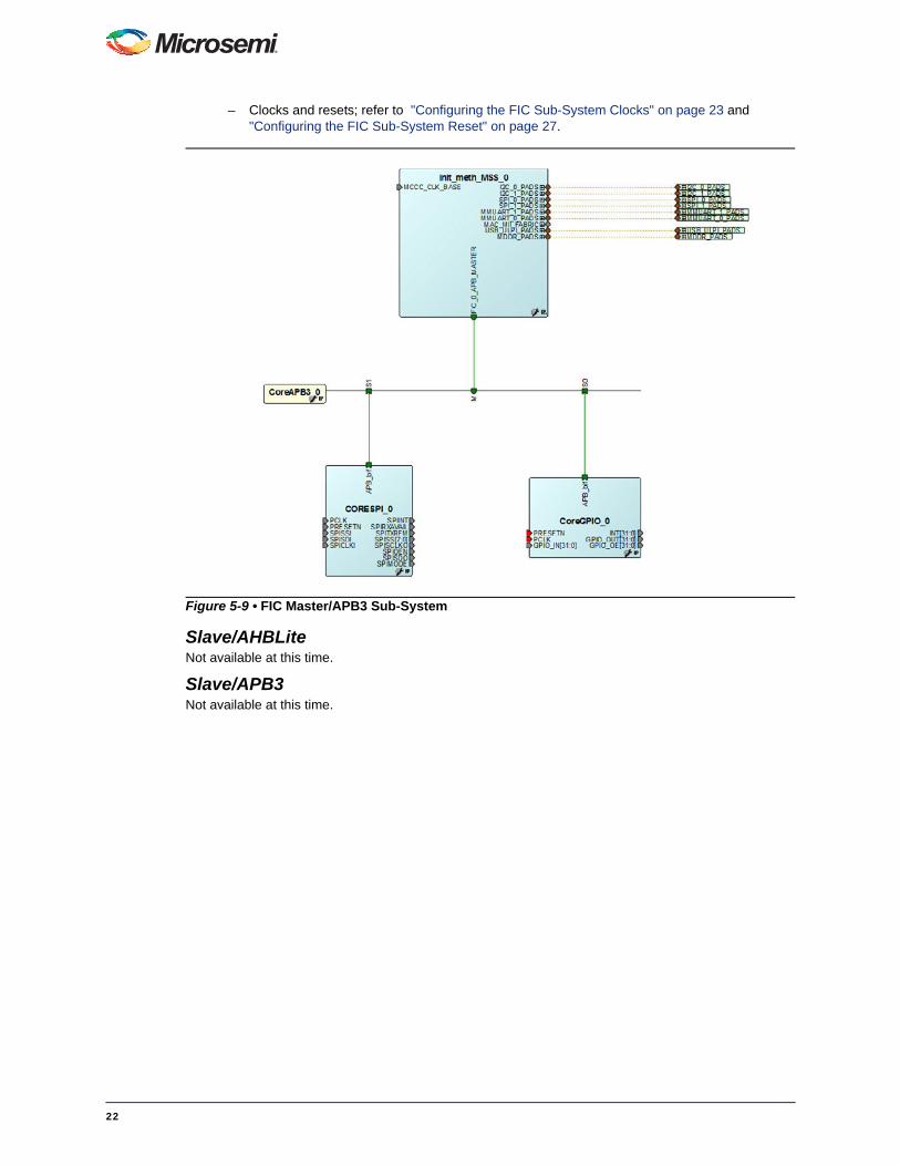
– Clocks and resets; refer to "Configuring the FIC Sub-System Clocks" on page 23 and "Configuring the FIC Sub-System Reset" on page 27.
Slave/AHBLiteNot available at this time.
Slave/APB3Not available at this time.
Figure 5-9 • FIC Master/APB3 Sub-System
22
6 – Configuring the FIC Sub-System Clocks
To create the proper clock configuration and connectivity, you must:
• Configure the MSS CCC FIC clocks
• Instantiate and configure an FPGA fabric CCC core
• Connect the clock networks for each FIC sub-system
• Connect the MSS CLK_BASE port to the correct FPGA fabric FIC sub-system clock network
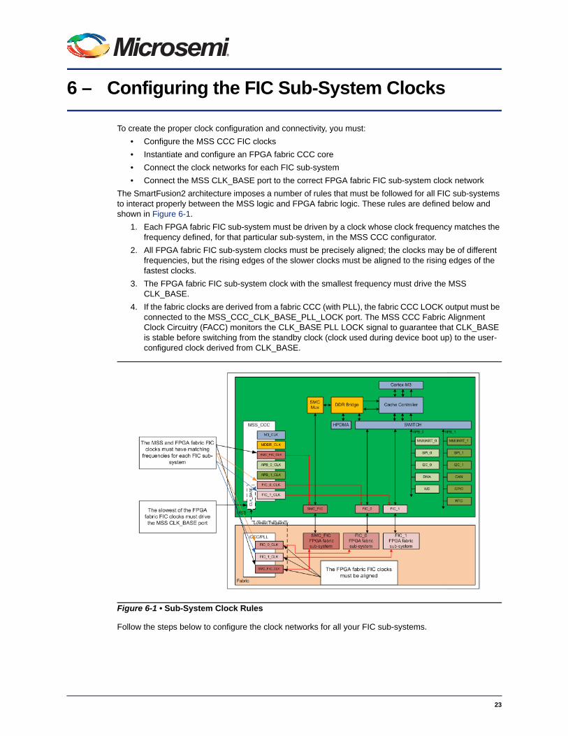
The SmartFusion2 architecture imposes a number of rules that must be followed for all FIC sub-systems to interact properly between the MSS logic and FPGA fabric logic. These rules are defined below and shown in Figure 6-1.
1. Each FPGA fabric FIC sub-system must be driven by a clock whose clock frequency matches the frequency defined, for that particular sub-system, in the MSS CCC configurator.
2. All FPGA fabric FIC sub-system clocks must be precisely aligned; the clocks may be of different frequencies, but the rising edges of the slower clocks must be aligned to the rising edges of the fastest clocks.
3. The FPGA fabric FIC sub-system clock with the smallest frequency must drive the MSS CLK_BASE.
4. If the fabric clocks are derived from a fabric CCC (with PLL), the fabric CCC LOCK output must be connected to the MSS_CCC_CLK_BASE_PLL_LOCK port. The MSS CCC Fabric Alignment Clock Circuitry (FACC) monitors the CLK_BASE PLL LOCK signal to guarantee that CLK_BASE is stable before switching from the standby clock (clock used during device boot up) to the user-configured clock derived from CLK_BASE.
Follow the steps below to configure the clock networks for all your FIC sub-systems.
Figure 6-1 • Sub-System Clock Rules
23
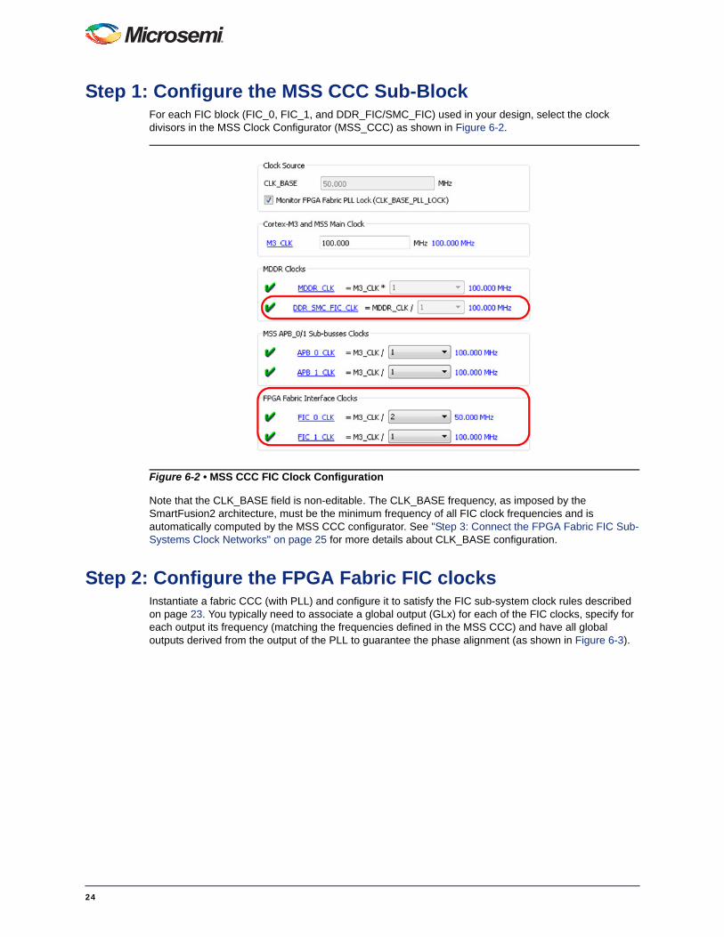
Step 1: Configure the MSS CCC Sub-BlockFor each FIC block (FIC_0, FIC_1, and DDR_FIC/SMC_FIC) used in your design, select the clock divisors in the MSS Clock Configurator (MSS_CCC) as shown in Figure 6-2.
Note that the CLK_BASE field is non-editable. The CLK_BASE frequency, as imposed by the SmartFusion2 architecture, must be the minimum frequency of all FIC clock frequencies and is automatically computed by the MSS CCC configurator. See "Step 3: Connect the FPGA Fabric FIC Sub-Systems Clock Networks" on page 25 for more details about CLK_BASE configuration.
Step 2: Configure the FPGA Fabric FIC clocksInstantiate a fabric CCC (with PLL) and configure it to satisfy the FIC sub-system clock rules described on page 23. You typically need to associate a global output (GLx) for each of the FIC clocks, specify for each output its frequency (matching the frequencies defined in the MSS CCC) and have all global outputs derived from the output of the PLL to guarantee the phase alignment (as shown in Figure 6-3).
Figure 6-2 • MSS CCC FIC Clock Configuration
24
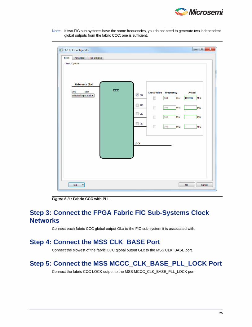
Note: If two FIC sub-systems have the same frequencies, you do not need to generate two independent global outputs from the fabric CCC; one is sufficient.
Step 3: Connect the FPGA Fabric FIC Sub-Systems Clock Networks
Connect each fabric CCC global output GLx to the FIC sub-system it is associated with.
Step 4: Connect the MSS CLK_BASE PortConnect the slowest of the fabric CCC global output GLx to the MSS CLK_BASE port.
Step 5: Connect the MSS MCCC_CLK_BASE_PLL_LOCK PortConnect the fabric CCC LOCK output to the MSS MCCC_CLK_BASE_PLL_LOCK port.
Figure 6-3 • Fabric CCC with PLL
25

Timing Analysis RequirementsPerform post-layout static timing analysis to make sure that the design meets the timing requirements defined in the MSS CCC and FPGA fabric CCC Configurators. You may have to change M3_CLK or increase the clock ratio between the MSS and the fabric to get a design that passes Static Timing Analysis.
26
27
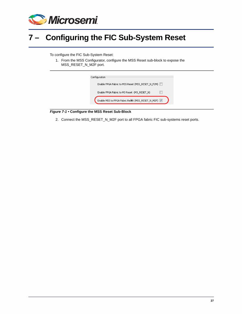
7 – Configuring the FIC Sub-System Reset
To configure the FIC Sub-System Reset:
1. From the MSS Configurator, configure the MSS Reset sub-block to expose the MSS_RESET_N_M2F port.
2. Connect the MSS_RESET_N_M2F port to all FPGA fabric FIC sub-systems reset ports.
Figure 7-1 • Configure the MSS Reset Sub-Block
8 – Configuring the System Memory Map
Each peripheral (AMBA AXI, AHBLite and APB3 slaves) is identified by an address from the FIC sub-system's master point of view. We usually refer to the overall relationships between masters and slaves of a sub-system as the memory map of that sub-system. The memory map of a sub-system can be edited in SmartDesign. You can also view the final memory map of your system when you generate the entire system. The memory map is part of the Datasheet generated for the 'root' of your design upon generation.
Configuring the Memory Map (Generic SmartDesign Behavior)
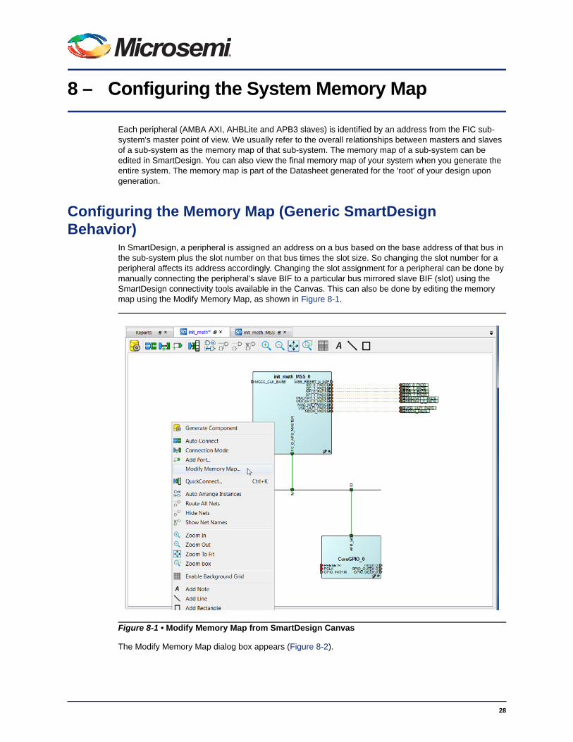
In SmartDesign, a peripheral is assigned an address on a bus based on the base address of that bus in the sub-system plus the slot number on that bus times the slot size. So changing the slot number for a peripheral affects its address accordingly. Changing the slot assignment for a peripheral can be done by manually connecting the peripheral's slave BIF to a particular bus mirrored slave BIF (slot) using the SmartDesign connectivity tools available in the Canvas. This can also be done by editing the memory map using the Modify Memory Map, as shown in Figure 8-1.
The Modify Memory Map dialog box appears (Figure 8-2).
Figure 8-1 • Modify Memory Map from SmartDesign Canvas
28
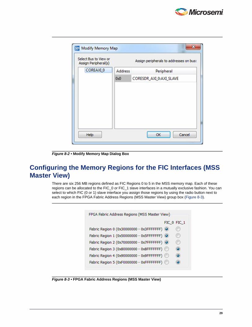
Configuring the Memory Regions for the FIC Interfaces (MSS Master View)
There are six 256 MB regions defined as FIC Regions 0 to 5 in the MSS memory map. Each of these regions can be allocated to the FIC_0 or FIC_1 slave interfaces in a mutually exclusive fashion. You can select to which FIC (0 or 1) slave interface you assign those regions by using the radio button next to each region in the FPGA Fabric Address Regions (MSS Master View) group box (Figure 8-3).
Figure 8-2 • Modify Memory Map Dialog Box
Figure 8-3 • FPGA Fabric Address Regions (MSS Master View)
29

Memory Map Computation General FormulaThe possible base addresses for the FIC fabric interfaces are 0x30000000, 0x50000000, 0x70000000, 0x80000000, 0x90000000 and 0xF0000000. See "Configuring the FIC Sub-Systems" on page 17 for details on how to configure each FIC instance to map to these addresses.
For AHBLite, the slot size can either be 16 MB (0x01000000) or 256 MB (0x10000000).
When using 16 MB per slot, all slots from 0 to 16 can be used; the address of client peripheral can be computed as the FIC memory region base address + (slot number * 0x01000000). In this configuration, all regions are actually aliases of each other as the AHBLite core does not decode the address bits [31:28]; the slots are decoded using address bits [27:24].
When using 256 MB per slot, only slots 3, 5, 7, 8, 9 and F can be used; the address of client peripheral can be computed as the FIC memory region base address + (slot number * 0x10000000). In this configuration, all regions uniquely address different slots as the AHBLite core decodes the slots using address bits [31:28]. In this configuration, to simplify the memory map equation, the base address is 0x00000000, instead of one of the six fixed address defined above.
Example 1 (16 MB slot configuration):Using memory region 0x50000000, if the peripheral is at slot number 7, then its address is:
0x50000000 + (0x7 * 0x01000000) = 0x57000000
Example 2 (256 MB slot configuration):Using memory region 0x50000000, if the peripheral is at slot number 15, then its address is:
0x00000000 + (0xF * 0x10000000) = 0xF0000000
Viewing the Final Memory MapAt this time, Libero SoC does not generate a correct memory map for systems using the SmartFusion2 MSS.
30
A – Product Support
Microsemi SoC Products Group backs its products with various support services, including Customer Service, Customer Technical Support Center, a website, electronic mail, and worldwide sales offices. This appendix contains information about contacting Microsemi SoC Products Group and using these support services.
Customer ServiceContact Customer Service for non-technical product support, such as product pricing, product upgrades, update information, order status, and authorization.
From North America, call 800.262.1060From the rest of the world, call 650.318.4460Fax, from anywhere in the world, 408.643.6913
Customer Technical Support CenterMicrosemi SoC Products Group staffs its Customer Technical Support Center with highly skilled engineers who can help answer your hardware, software, and design questions about Microsemi SoC Products. The Customer Technical Support Center spends a great deal of time creating application notes, answers to common design cycle questions, documentation of known issues, and various FAQs. So, before you contact us, please visit our online resources. It is very likely we have already answered your questions.
Technical SupportVisit the Customer Support website (www.microsemi.com/soc/support/search/default.aspx) for more information and support. Many answers available on the searchable web resource include diagrams, illustrations, and links to other resources on the website.
WebsiteYou can browse a variety of technical and non-technical information on the SoC home page, at www.microsemi.com/soc.
Contacting the Customer Technical Support CenterHighly skilled engineers staff the Technical Support Center. The Technical Support Center can be contacted by email or through the Microsemi SoC Products Group website.
EmailYou can communicate your technical questions to our email address and receive answers back by email, fax, or phone. Also, if you have design problems, you can email your design files to receive assistance. We constantly monitor the email account throughout the day. When sending your request to us, please be sure to include your full name, company name, and your contact information for efficient processing of your request.
The technical support email address is [email protected].
31
MOWSaFa
Microsemi Corporation (NASDAQ: MSCC) offers a comprehensive portfolio of semiconductorsolutions for: aerospace, defense and security; enterprise and communications; and industrialand alternative energy markets. Products include high-performance, high-reliability analogand RF devices, mixed signal and RF integrated circuits, customizable SoCs, FPGAs, andcomplete subsystems. Microsemi is headquartered in Aliso Viejo, Calif. Learn more atwww.microsemi.com.
icrosemi Corporate Headquarters
My CasesMicrosemi SoC Products Group customers may submit and track technical cases online by going to My Cases.
Outside the U.S.Customers needing assistance outside the US time zones can either contact technical support via email ([email protected]) or contact a local sales office. Sales office listings can be found at www.microsemi.com/soc/company/contact/default.aspx.
ITAR Technical SupportFor technical support on RH and RT FPGAs that are regulated by International Traffic in Arms Regulations (ITAR), contact us via [email protected]. Alternatively, within My Cases, select Yes in the ITAR drop-down list. For a complete list of ITAR-regulated Microsemi FPGAs, visit the ITAR web page.
5-02-00370-1/08.14
© 2014 Microsemi Corporation. All rights reserved. Microsemi and the Microsemi logo are trademarks ofMicrosemi Corporation. All other trademarks and service marks are the property of their respective owners.
ne Enterprise, Aliso Viejo CA 92656 USAithin the USA: +1 (949) 380-6100les: +1 (949) 380-6136x: +1 (949) 215-4996