Embed Size (px)
Citation preview
SmartFusion2 MSSDDR Controller Configuration
SmartFusion2 MSS DDR Controller Configuration
2
Table of Contents
Introduction . . . . . . . . . . . . . . . . . . . . . . . . . . . . . . . . . . . . . . . . . . . . . . . . . . . . . . . . . . . . . . . . . . . . . . 3
1 MDDR Configurator . . . . . . . . . . . . . . . . . . . . . . . . . . . . . . . . . . . . . . . . . . . . . . . . . . . . . . . . . . . . . . . . 4
2 MDDR Controller Configuration . . . . . . . . . . . . . . . . . . . . . . . . . . . . . . . . . . . . . . . . . . . . . . . . . . . . . . . 6MSS DDR Control Registers . . . . . . . . . . . . . . . . . . . . . . . . . . . . . . . . . . . . . . . . . . . . . . . . . . . . . . . . . . . . . . . . . . 6
Importing DDR Configuration Files . . . . . . . . . . . . . . . . . . . . . . . . . . . . . . . . . . . . . . . . . . . . . . . . . . . . . . . . . . . . . 7
Exporting DDR Configuration Files . . . . . . . . . . . . . . . . . . . . . . . . . . . . . . . . . . . . . . . . . . . . . . . . . . . . . . . . . . . . . 8
Firmware . . . . . . . . . . . . . . . . . . . . . . . . . . . . . . . . . . . . . . . . . . . . . . . . . . . . . . . . . . . . . . . . . . . . . . . . . . . . . . . . . 9
MSS DDR Configuration Path . . . . . . . . . . . . . . . . . . . . . . . . . . . . . . . . . . . . . . . . . . . . . . . . . . . . . . . . . . . . . . . . 10
3 Port Description . . . . . . . . . . . . . . . . . . . . . . . . . . . . . . . . . . . . . . . . . . . . . . . . . . . . . . . . . . . . . . . . . . 12
A Product Support . . . . . . . . . . . . . . . . . . . . . . . . . . . . . . . . . . . . . . . . . . . . . . . . . . . . . . . . . . . . . . . . . . 19Customer Service . . . . . . . . . . . . . . . . . . . . . . . . . . . . . . . . . . . . . . . . . . . . . . . . . . . . . . . . . . . . . . . . . . . . . . . . . 19
Customer Technical Support Center . . . . . . . . . . . . . . . . . . . . . . . . . . . . . . . . . . . . . . . . . . . . . . . . . . . . . . . . . . . 19
Technical Support . . . . . . . . . . . . . . . . . . . . . . . . . . . . . . . . . . . . . . . . . . . . . . . . . . . . . . . . . . . . . . . . . . . . . . . . . 19
Website . . . . . . . . . . . . . . . . . . . . . . . . . . . . . . . . . . . . . . . . . . . . . . . . . . . . . . . . . . . . . . . . . . . . . . . . . . . . . . . . . 19
Contacting the Customer Technical Support Center . . . . . . . . . . . . . . . . . . . . . . . . . . . . . . . . . . . . . . . . . . . . . . . 19
ITAR Technical Support . . . . . . . . . . . . . . . . . . . . . . . . . . . . . . . . . . . . . . . . . . . . . . . . . . . . . . . . . . . . . . . . . . . . . 20
3
Introduction
The SmartFusion2 MSS has an embedded DDR controller. This DDR controller is intended to control an off-chip DDR memory. The MDDR controller can be accessed from the MSS as well as from the FPGA fabric. In addition, the DDR controller can also be bypassed, providing an additional interface to the FPGA fabric (Soft Controller Mode (SMC)).
To fully configure the MSS DDR controller you must:
1. Select the datapath using the MDDR Configurator.
2. Set the register values for the DDR controller registers.
3. Select the DDR memory clock frequencies and FPGA fabric to MDDR clock ratio (if needed)using the MSS CCC Configurator.
4. Connect the controller's APB configuration interface as defined by the Peripheral Initializationsolution.
1 – MDDR Configurator
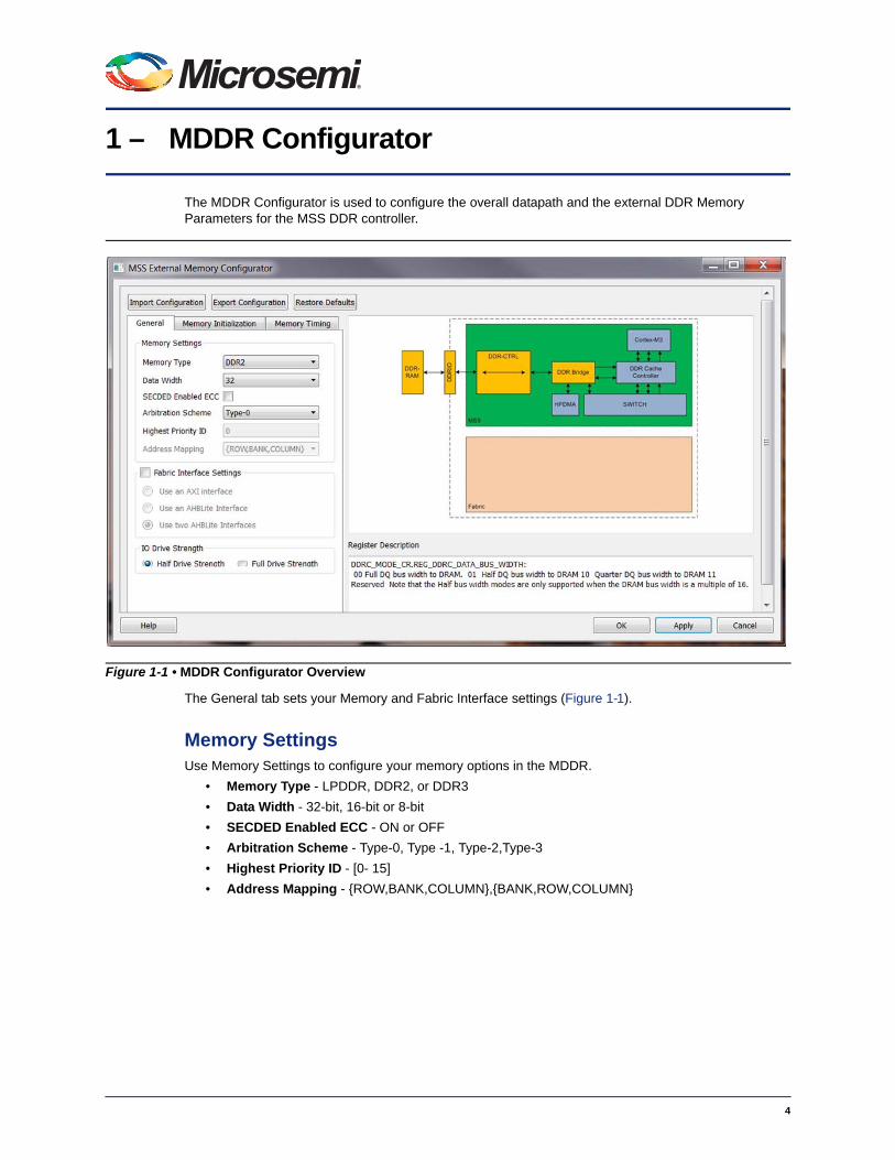
The MDDR Configurator is used to configure the overall datapath and the external DDR Memory Parameters for the MSS DDR controller.
The General tab sets your Memory and Fabric Interface settings (Figure 1-1).
Memory SettingsUse Memory Settings to configure your memory options in the MDDR.
• Memory Type - LPDDR, DDR2, or DDR3
• Data Width - 32-bit, 16-bit or 8-bit
• SECDED Enabled ECC - ON or OFF
• Arbitration Scheme - Type-0, Type -1, Type-2,Type-3
• Highest Priority ID - [0- 15]
• Address Mapping - {ROW,BANK,COLUMN},{BANK,ROW,COLUMN}
Figure 1-1 • MDDR Configurator Overview
4
Fabric Interface SettingsBy default, the hard Cortex-M3 processor is set up to access the DDR Controller. You can also allow a fabric Master to access the DDR Controller by enabling the Fabric Interface Setting checkbox. In this case, you can choose one of the following options:
• Use an AXI Interface - The fabric Master accesses the DDR Controller through a 64-bit AXI interface.
• Use a Single AHBLite Interface - The fabric Master accesses the DDR Controller through a single 32-bit AHB interface.
• Use two AHBLite Interfaces - Two fabric Masters access the DDR Controller using two 32-bit AHB interfaces.
The configuration view (Figure 1-1) updates according to your Fabric Interface selection.
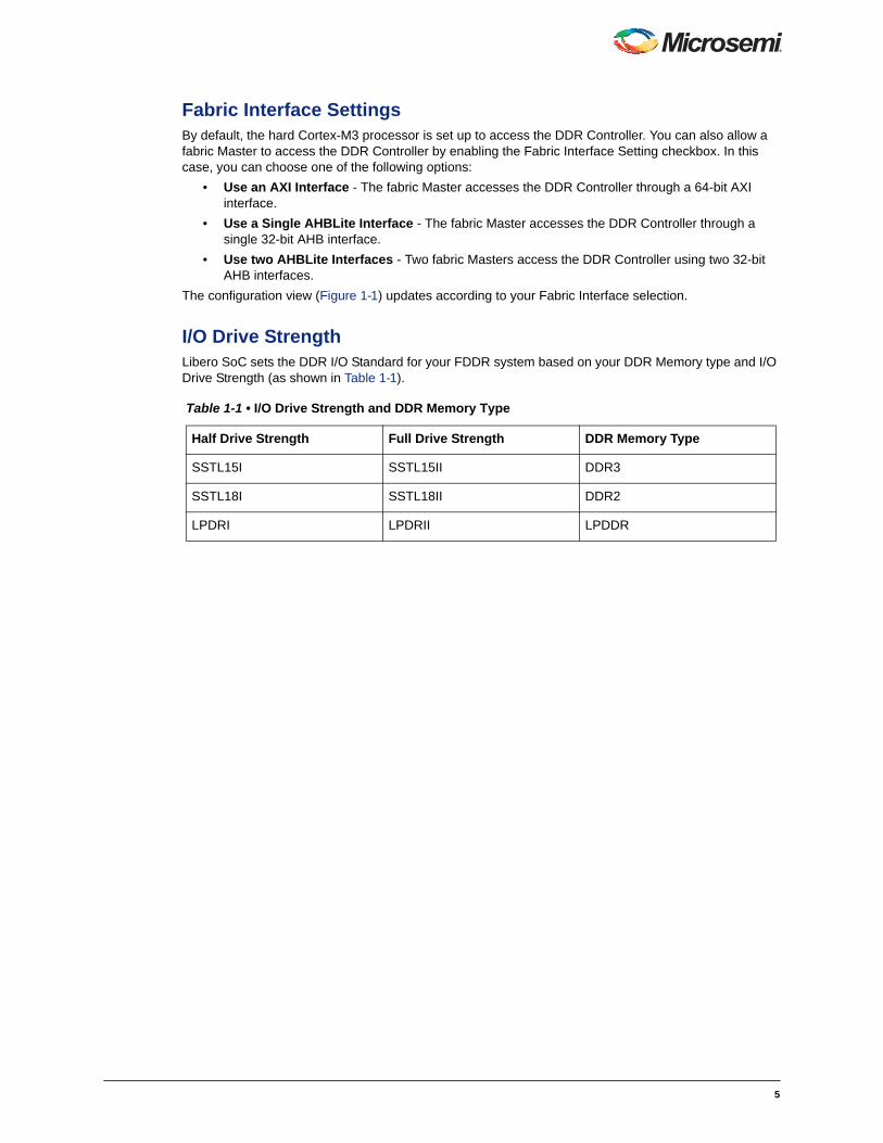
I/O Drive StrengthLibero SoC sets the DDR I/O Standard for your FDDR system based on your DDR Memory type and I/O Drive Strength (as shown in Table 1-1).
Table 1-1 • I/O Drive Strength and DDR Memory Type
Half Drive Strength Full Drive Strength DDR Memory Type
SSTL15I SSTL15II DDR3
SSTL18I SSTL18II DDR2
LPDRI LPDRII LPDDR
5
2 – MDDR Controller Configuration
When you use the MSS DDR Controller to access an external DDR Memory, the DDR Controller must be configured at runtime. This is done by writing configuration data to dedicated DDR controller configuration registers. This configuration data is dependent on the characteristics of the external DDR memory and your application. In this section, we describe how to enter these configuration parameters in the MSS DDR controller configurator and how the configuration data is managed as part of the overall Peripheral Initialization solution. Refer to the Peripheral Initialization User Guide for detailed information about the peripheral initialization solution.
MSS DDR Control RegistersThe MSS DDR Controller has a set of registers that need to be configured at runtime. The configuration values for these registers represent different parameters, such as DDR mode, PHY width, burst mode, and ECC. For complete details about the DDR controller configuration registers please refer to the Microsemi SmartFusion2 User's Guide
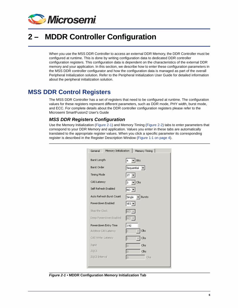
MSS DDR Registers ConfigurationUse the Memory Initialization (Figure 2-1) and Memory Timing (Figure 2-2) tabs to enter parameters that correspond to your DDR Memory and application. Values you enter in these tabs are automatically translated to the appropriate register values. When you click a specific parameter its corresponding register is described in the Register Description Window (Figure 1-1 on page 4).
Figure 2-1 • MDDR Configuration Memory Initialization Tab
6
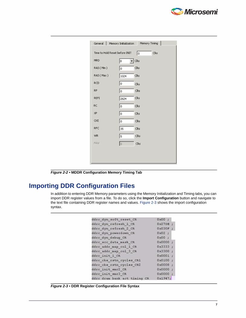
Importing DDR Configuration FilesIn addition to entering DDR Memory parameters using the Memory Initialization and Timing tabs, you can import DDR register values from a file. To do so, click the Import Configuration button and navigate to the text file containing DDR register names and values. Figure 2-3 shows the import configuration syntax.
Figure 2-2 • MDDR Configuration Memory Timing Tab
Figure 2-3 • DDR Register Configuration File Syntax
7
Note: If you choose to import register values rather than entering them using the GUI, you must specify all necessary register values. Consult the SmartFusion2 User Guide for details.
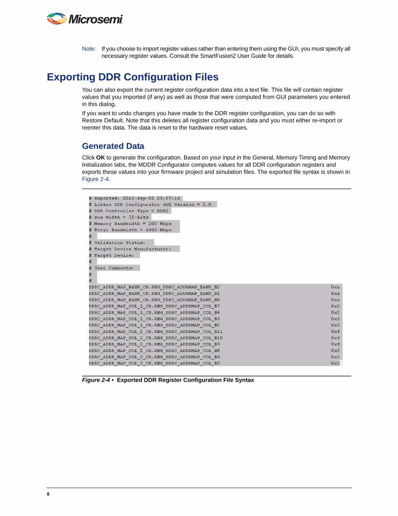
Exporting DDR Configuration FilesYou can also export the current register configuration data into a text file. This file will contain register values that you imported (if any) as well as those that were computed from GUI parameters you entered in this dialog.
If you want to undo changes you have made to the DDR register configuration, you can do so with Restore Default. Note that this deletes all register configuration data and you must either re-import or reenter this data. The data is reset to the hardware reset values.
Generated DataClick OK to generate the configuration. Based on your input in the General, Memory Timing and Memory Initialization tabs, the MDDR Configurator computes values for all DDR configuration registers and exports these values into your firmware project and simulation files. The exported file syntax is shown in Figure 2-4.
Figure 2-4 • Exported DDR Register Configuration File Syntax
8
FirmwareWhen you generate the SmartDesign, the following files are generated in the <project dir>/firmware/drivers_config/sys_config directory. These files are required for the CMSIS firmware core to compile properly and contain information regarding your current design including peripheral configuration data and clock configuration information for the MSS. Do not edit these files manually as they are re-created every time your root design is re-generated.
• sys_config.c
• sys_config.h
• sys_config_mddr_define.h - MDDR configuration data.
• Sys_config_fddr_define.h - FDDR configuration data.
• sys_config_mss_clocks.h - MSS clocks configuration
SimulationWhen you generate the SmartDesign associated with your MSS, the following simulation files are generated in the <project dir>/simulation directory:
• test.bfm - Top-level BFM file that is first "executed" during any simulation that exercises the SmartFusion2 MSS' Cortex-M3 processor. It executes peripheral_init.bfm and user.bfm, in that order.
• peripheral_init.bfm - Contains the BFM procedure that emulates the CMSIS::SystemInit() function run on the Cortex-M3 before you enter the main() procedure. It essentially copies the configuration data for any peripheral used in the design to the correct peripheral configuration registers and then waits for all the peripherals to be ready before asserting that the user can use these peripherals.
• MDDR_init.bfm - Contains BFM write commands that simulate writes of the MSS DDR configuration register data you entered (using the Edit Registers dialog above) into the DDR Controller registers.
• user.bfm - Intended for user commands. You can simulate the datapath by adding your own BFM commands in this file. Commands in this file will be "executed" after peripheral_init.bfm has completed.
Using the files above, the configuration path is simulated automatically. You only need to edit the user.bfm file to simulate the datapath. Do not edit the test.bfm, peripheral_init.bfm, or MDDR_init.bfm files as these files are re-created every time your root design is re-generated.
9
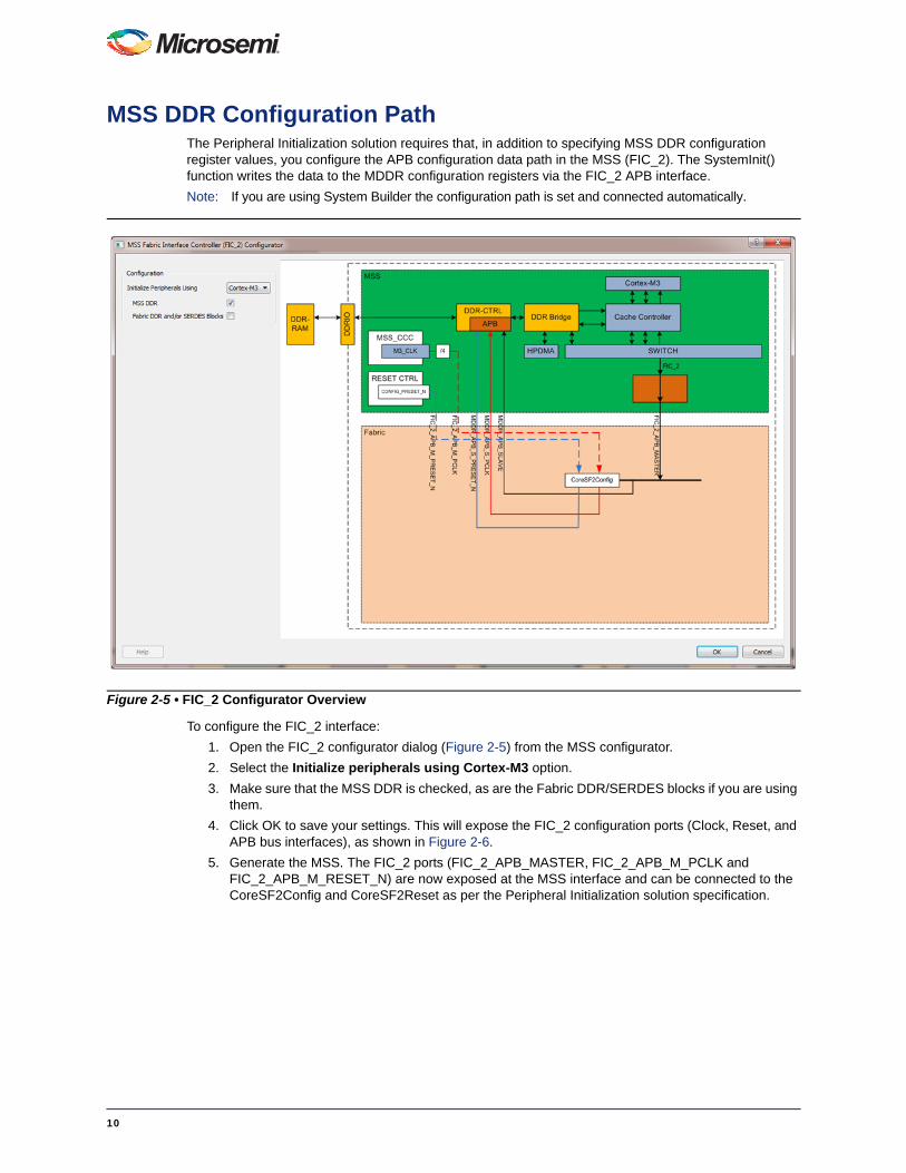
MSS DDR Configuration PathThe Peripheral Initialization solution requires that, in addition to specifying MSS DDR configuration register values, you configure the APB configuration data path in the MSS (FIC_2). The SystemInit() function writes the data to the MDDR configuration registers via the FIC_2 APB interface.
Note: If you are using System Builder the configuration path is set and connected automatically.
To configure the FIC_2 interface:
1. Open the FIC_2 configurator dialog (Figure 2-5) from the MSS configurator.
2. Select the Initialize peripherals using Cortex-M3 option.
3. Make sure that the MSS DDR is checked, as are the Fabric DDR/SERDES blocks if you are using them.
4. Click OK to save your settings. This will expose the FIC_2 configuration ports (Clock, Reset, and APB bus interfaces), as shown in Figure 2-6.
5. Generate the MSS. The FIC_2 ports (FIC_2_APB_MASTER, FIC_2_APB_M_PCLK and FIC_2_APB_M_RESET_N) are now exposed at the MSS interface and can be connected to the CoreSF2Config and CoreSF2Reset as per the Peripheral Initialization solution specification.
Figure 2-5 • FIC_2 Configurator Overview
10
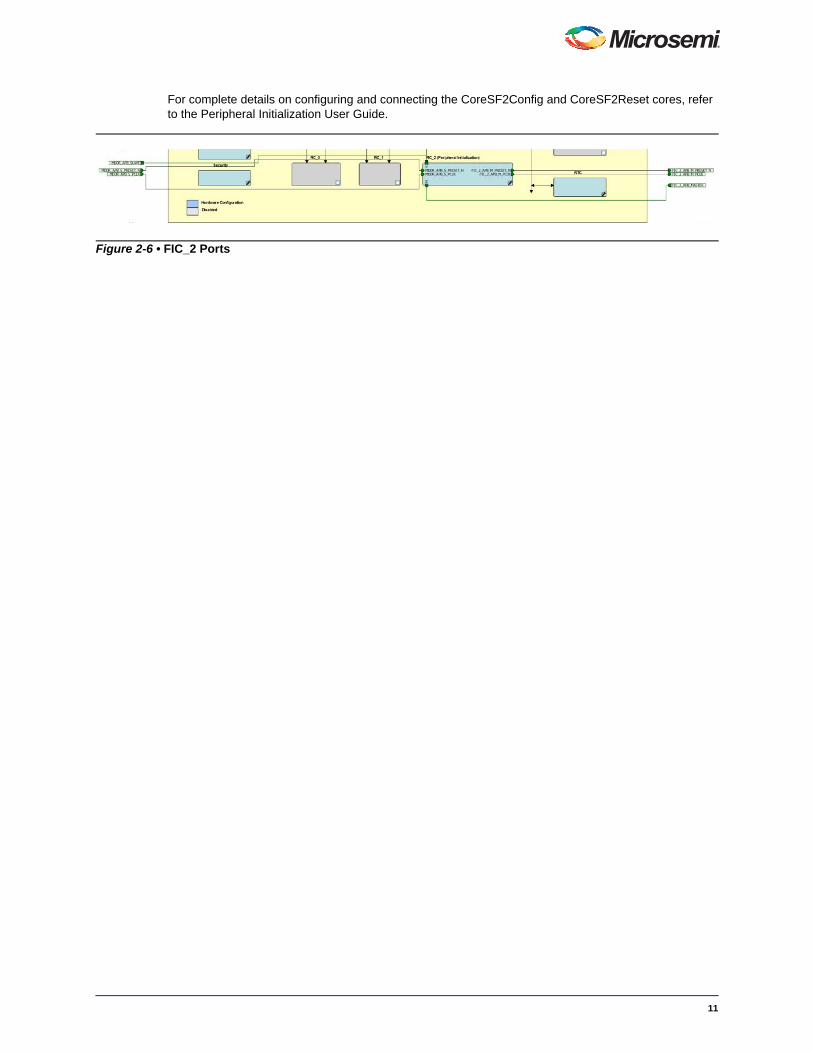
For complete details on configuring and connecting the CoreSF2Config and CoreSF2Reset cores, refer to the Peripheral Initialization User Guide.
Figure 2-6 • FIC_2 Ports
11
3 – Port Description
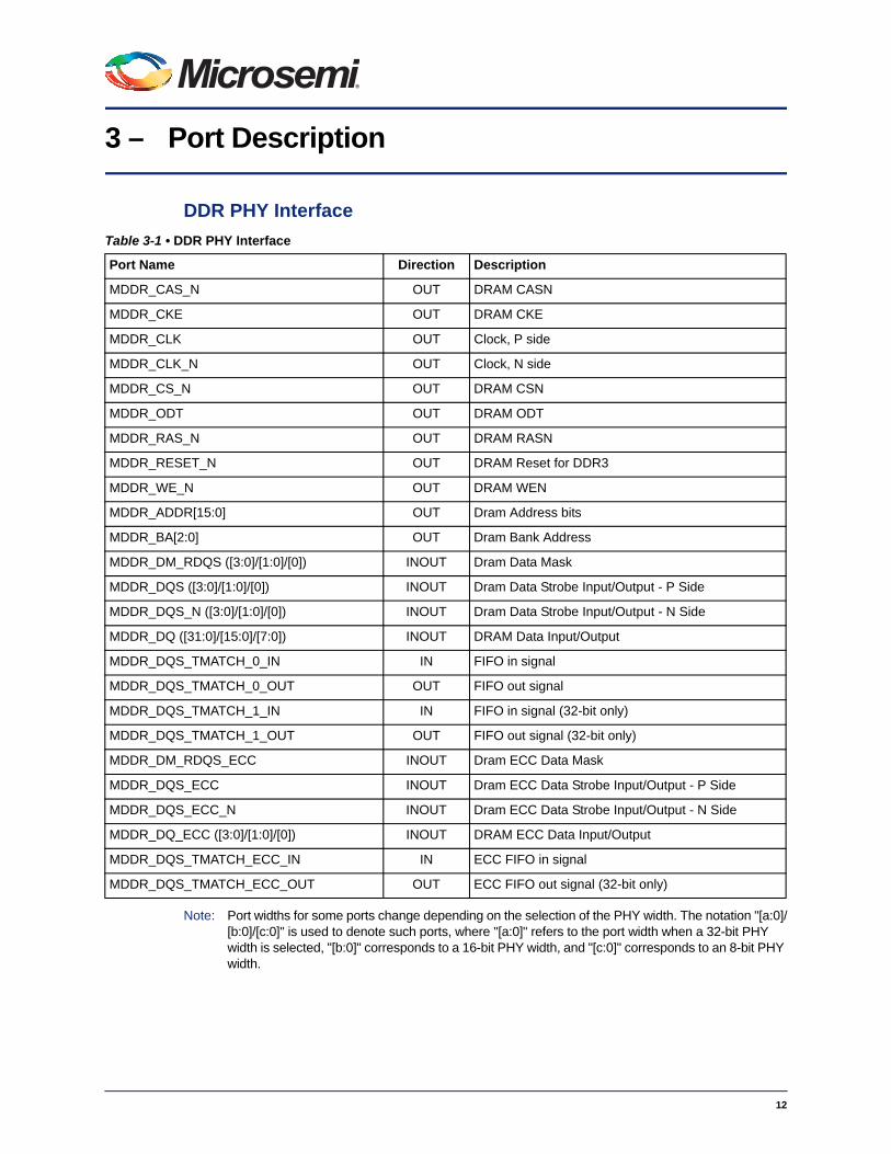
DDR PHY Interface
Note: Port widths for some ports change depending on the selection of the PHY width. The notation "[a:0]/[b:0]/[c:0]" is used to denote such ports, where "[a:0]" refers to the port width when a 32-bit PHY width is selected, "[b:0]" corresponds to a 16-bit PHY width, and "[c:0]" corresponds to an 8-bit PHY width.
Table 3-1 • DDR PHY Interface
Port Name Direction Description
MDDR_CAS_N OUT DRAM CASN
MDDR_CKE OUT DRAM CKE
MDDR_CLK OUT Clock, P side
MDDR_CLK_N OUT Clock, N side
MDDR_CS_N OUT DRAM CSN
MDDR_ODT OUT DRAM ODT
MDDR_RAS_N OUT DRAM RASN
MDDR_RESET_N OUT DRAM Reset for DDR3
MDDR_WE_N OUT DRAM WEN
MDDR_ADDR[15:0] OUT Dram Address bits
MDDR_BA[2:0] OUT Dram Bank Address
MDDR_DM_RDQS ([3:0]/[1:0]/[0]) INOUT Dram Data Mask
MDDR_DQS ([3:0]/[1:0]/[0]) INOUT Dram Data Strobe Input/Output - P Side
MDDR_DQS_N ([3:0]/[1:0]/[0]) INOUT Dram Data Strobe Input/Output - N Side
MDDR_DQ ([31:0]/[15:0]/[7:0]) INOUT DRAM Data Input/Output
MDDR_DQS_TMATCH_0_IN IN FIFO in signal
MDDR_DQS_TMATCH_0_OUT OUT FIFO out signal
MDDR_DQS_TMATCH_1_IN IN FIFO in signal (32-bit only)
MDDR_DQS_TMATCH_1_OUT OUT FIFO out signal (32-bit only)
MDDR_DM_RDQS_ECC INOUT Dram ECC Data Mask
MDDR_DQS_ECC INOUT Dram ECC Data Strobe Input/Output - P Side
MDDR_DQS_ECC_N INOUT Dram ECC Data Strobe Input/Output - N Side
MDDR_DQ_ECC ([3:0]/[1:0]/[0]) INOUT DRAM ECC Data Input/Output
MDDR_DQS_TMATCH_ECC_IN IN ECC FIFO in signal
MDDR_DQS_TMATCH_ECC_OUT OUT ECC FIFO out signal (32-bit only)
12
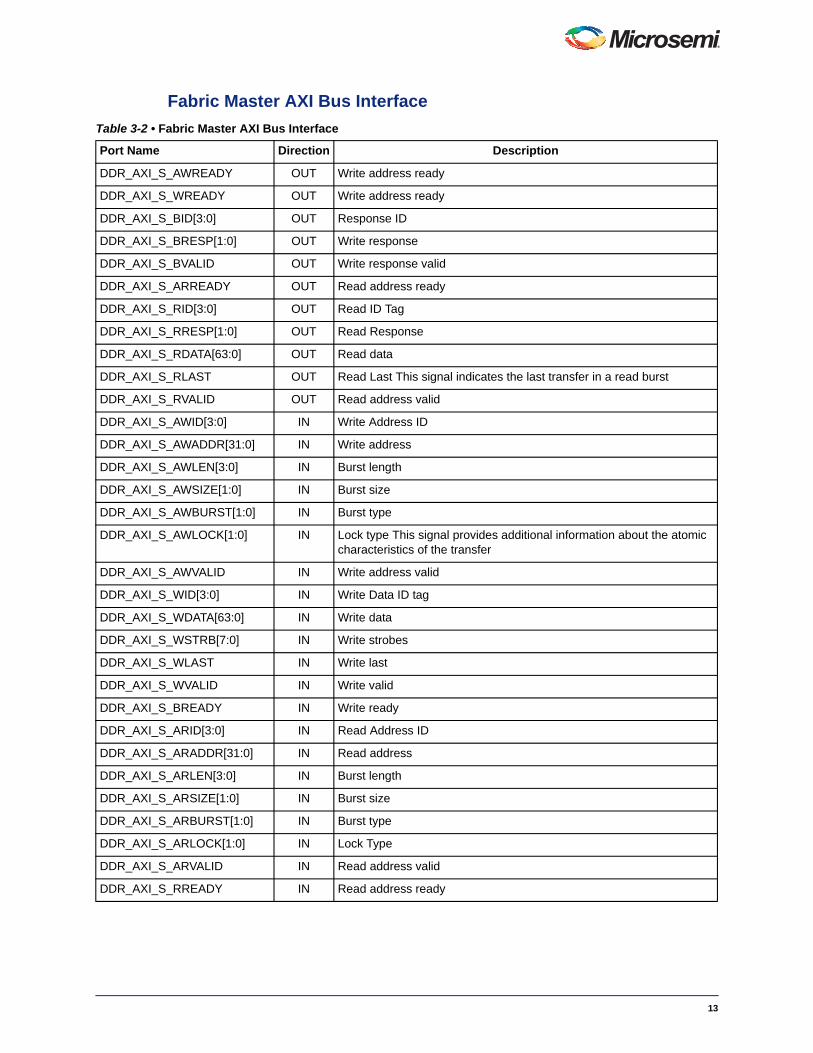
Fabric Master AXI Bus Interface
Table 3-2 • Fabric Master AXI Bus Interface
Port Name Direction Description
DDR_AXI_S_AWREADY OUT Write address ready
DDR_AXI_S_WREADY OUT Write address ready
DDR_AXI_S_BID[3:0] OUT Response ID
DDR_AXI_S_BRESP[1:0] OUT Write response
DDR_AXI_S_BVALID OUT Write response valid
DDR_AXI_S_ARREADY OUT Read address ready
DDR_AXI_S_RID[3:0] OUT Read ID Tag
DDR_AXI_S_RRESP[1:0] OUT Read Response
DDR_AXI_S_RDATA[63:0] OUT Read data
DDR_AXI_S_RLAST OUT Read Last This signal indicates the last transfer in a read burst
DDR_AXI_S_RVALID OUT Read address valid
DDR_AXI_S_AWID[3:0] IN Write Address ID
DDR_AXI_S_AWADDR[31:0] IN Write address
DDR_AXI_S_AWLEN[3:0] IN Burst length
DDR_AXI_S_AWSIZE[1:0] IN Burst size
DDR_AXI_S_AWBURST[1:0] IN Burst type
DDR_AXI_S_AWLOCK[1:0] IN Lock type This signal provides additional information about the atomic characteristics of the transfer
DDR_AXI_S_AWVALID IN Write address valid
DDR_AXI_S_WID[3:0] IN Write Data ID tag
DDR_AXI_S_WDATA[63:0] IN Write data
DDR_AXI_S_WSTRB[7:0] IN Write strobes
DDR_AXI_S_WLAST IN Write last
DDR_AXI_S_WVALID IN Write valid
DDR_AXI_S_BREADY IN Write ready
DDR_AXI_S_ARID[3:0] IN Read Address ID
DDR_AXI_S_ARADDR[31:0] IN Read address
DDR_AXI_S_ARLEN[3:0] IN Burst length
DDR_AXI_S_ARSIZE[1:0] IN Burst size
DDR_AXI_S_ARBURST[1:0] IN Burst type
DDR_AXI_S_ARLOCK[1:0] IN Lock Type
DDR_AXI_S_ARVALID IN Read address valid
DDR_AXI_S_RREADY IN Read address ready
13
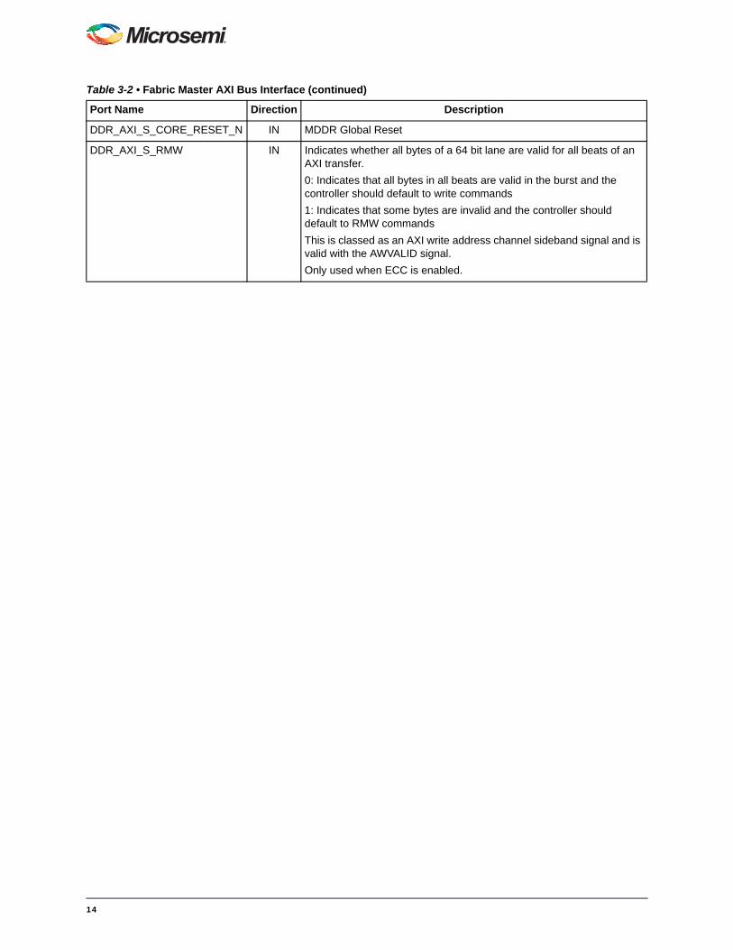
DDR_AXI_S_CORE_RESET_N IN MDDR Global Reset
DDR_AXI_S_RMW IN Indicates whether all bytes of a 64 bit lane are valid for all beats of an AXI transfer.
0: Indicates that all bytes in all beats are valid in the burst and the controller should default to write commands
1: Indicates that some bytes are invalid and the controller should default to RMW commands
This is classed as an AXI write address channel sideband signal and is valid with the AWVALID signal.
Only used when ECC is enabled.
Table 3-2 • Fabric Master AXI Bus Interface (continued)
Port Name Direction Description
14
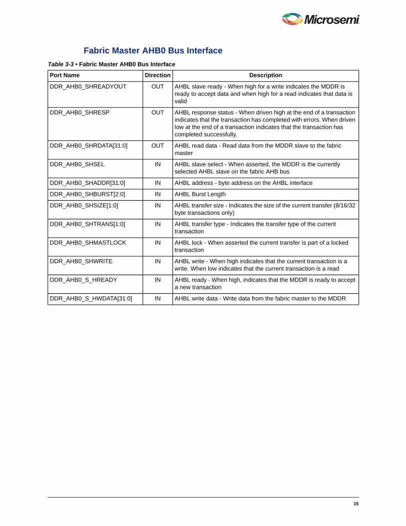
Fabric Master AHB0 Bus Interface
Table 3-3 • Fabric Master AHB0 Bus Interface
Port Name Direction Description
DDR_AHB0_SHREADYOUT OUT AHBL slave ready - When high for a write indicates the MDDR is ready to accept data and when high for a read indicates that data is valid
DDR_AHB0_SHRESP OUT AHBL response status - When driven high at the end of a transaction indicates that the transaction has completed with errors. When driven low at the end of a transaction indicates that the transaction has completed successfully.
DDR_AHB0_SHRDATA[31:0] OUT AHBL read data - Read data from the MDDR slave to the fabric master
DDR_AHB0_SHSEL IN AHBL slave select - When asserted, the MDDR is the currently selected AHBL slave on the fabric AHB bus
DDR_AHB0_SHADDR[31:0] IN AHBL address - byte address on the AHBL interface
DDR_AHB0_SHBURST[2:0] IN AHBL Burst Length
DDR_AHB0_SHSIZE[1:0] IN AHBL transfer size - Indicates the size of the current transfer (8/16/32 byte transactions only)
DDR_AHB0_SHTRANS[1:0] IN AHBL transfer type - Indicates the transfer type of the current transaction
DDR_AHB0_SHMASTLOCK IN AHBL lock - When asserted the current transfer is part of a locked transaction
DDR_AHB0_SHWRITE IN AHBL write - When high indicates that the current transaction is a write. When low indicates that the current transaction is a read
DDR_AHB0_S_HREADY IN AHBL ready - When high, indicates that the MDDR is ready to accept a new transaction
DDR_AHB0_S_HWDATA[31:0] IN AHBL write data - Write data from the fabric master to the MDDR
15
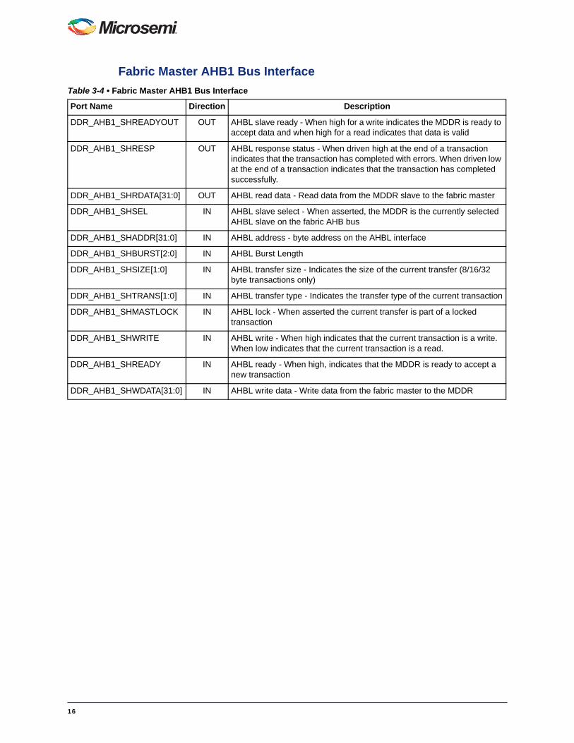
Fabric Master AHB1 Bus Interface
Table 3-4 • Fabric Master AHB1 Bus Interface
Port Name Direction Description
DDR_AHB1_SHREADYOUT OUT AHBL slave ready - When high for a write indicates the MDDR is ready to accept data and when high for a read indicates that data is valid
DDR_AHB1_SHRESP OUT AHBL response status - When driven high at the end of a transaction indicates that the transaction has completed with errors. When driven low at the end of a transaction indicates that the transaction has completed successfully.
DDR_AHB1_SHRDATA[31:0] OUT AHBL read data - Read data from the MDDR slave to the fabric master
DDR_AHB1_SHSEL IN AHBL slave select - When asserted, the MDDR is the currently selected AHBL slave on the fabric AHB bus
DDR_AHB1_SHADDR[31:0] IN AHBL address - byte address on the AHBL interface
DDR_AHB1_SHBURST[2:0] IN AHBL Burst Length
DDR_AHB1_SHSIZE[1:0] IN AHBL transfer size - Indicates the size of the current transfer (8/16/32 byte transactions only)
DDR_AHB1_SHTRANS[1:0] IN AHBL transfer type - Indicates the transfer type of the current transaction
DDR_AHB1_SHMASTLOCK IN AHBL lock - When asserted the current transfer is part of a locked transaction
DDR_AHB1_SHWRITE IN AHBL write - When high indicates that the current transaction is a write. When low indicates that the current transaction is a read.
DDR_AHB1_SHREADY IN AHBL ready - When high, indicates that the MDDR is ready to accept a new transaction
DDR_AHB1_SHWDATA[31:0] IN AHBL write data - Write data from the fabric master to the MDDR
16
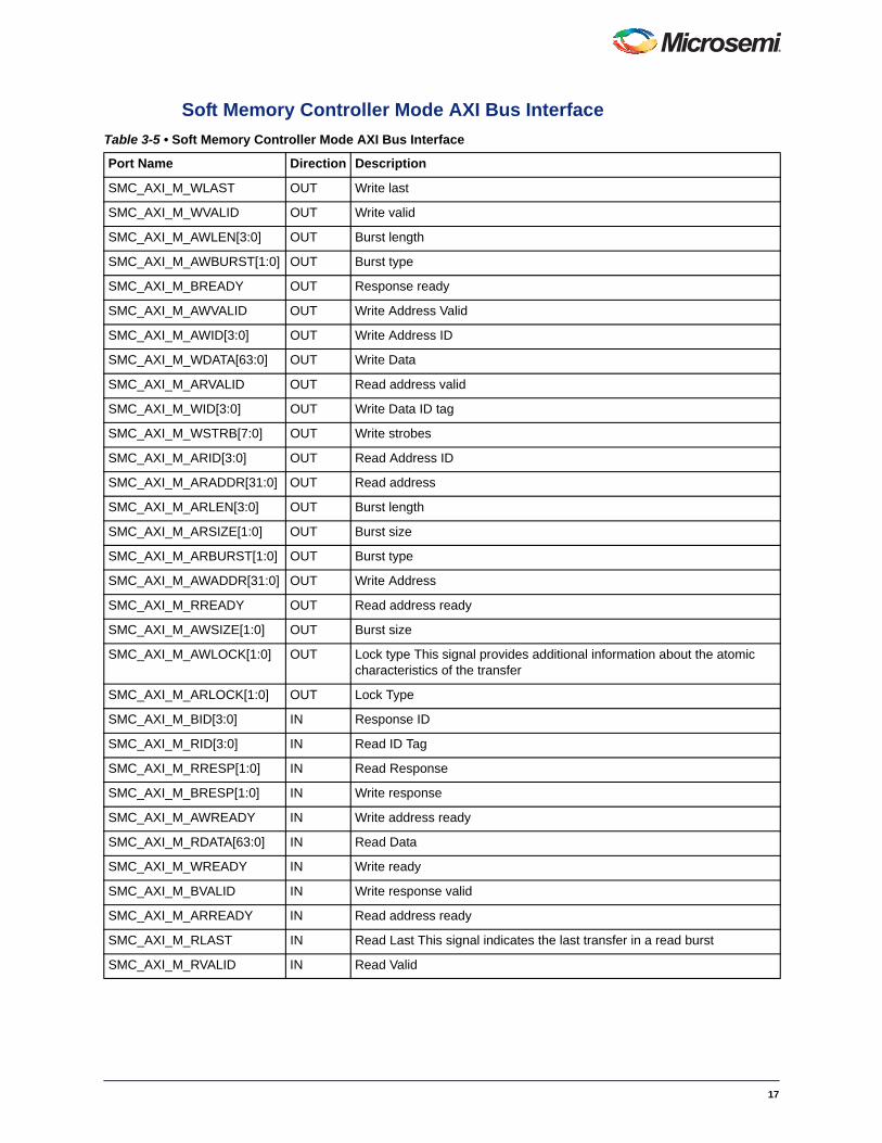
Soft Memory Controller Mode AXI Bus Interface
Table 3-5 • Soft Memory Controller Mode AXI Bus Interface
Port Name Direction Description
SMC_AXI_M_WLAST OUT Write last
SMC_AXI_M_WVALID OUT Write valid
SMC_AXI_M_AWLEN[3:0] OUT Burst length
SMC_AXI_M_AWBURST[1:0] OUT Burst type
SMC_AXI_M_BREADY OUT Response ready
SMC_AXI_M_AWVALID OUT Write Address Valid
SMC_AXI_M_AWID[3:0] OUT Write Address ID
SMC_AXI_M_WDATA[63:0] OUT Write Data
SMC_AXI_M_ARVALID OUT Read address valid
SMC_AXI_M_WID[3:0] OUT Write Data ID tag
SMC_AXI_M_WSTRB[7:0] OUT Write strobes
SMC_AXI_M_ARID[3:0] OUT Read Address ID
SMC_AXI_M_ARADDR[31:0] OUT Read address
SMC_AXI_M_ARLEN[3:0] OUT Burst length
SMC_AXI_M_ARSIZE[1:0] OUT Burst size
SMC_AXI_M_ARBURST[1:0] OUT Burst type
SMC_AXI_M_AWADDR[31:0] OUT Write Address
SMC_AXI_M_RREADY OUT Read address ready
SMC_AXI_M_AWSIZE[1:0] OUT Burst size
SMC_AXI_M_AWLOCK[1:0] OUT Lock type This signal provides additional information about the atomic characteristics of the transfer
SMC_AXI_M_ARLOCK[1:0] OUT Lock Type
SMC_AXI_M_BID[3:0] IN Response ID
SMC_AXI_M_RID[3:0] IN Read ID Tag
SMC_AXI_M_RRESP[1:0] IN Read Response
SMC_AXI_M_BRESP[1:0] IN Write response
SMC_AXI_M_AWREADY IN Write address ready
SMC_AXI_M_RDATA[63:0] IN Read Data
SMC_AXI_M_WREADY IN Write ready
SMC_AXI_M_BVALID IN Write response valid
SMC_AXI_M_ARREADY IN Read address ready
SMC_AXI_M_RLAST IN Read Last This signal indicates the last transfer in a read burst
SMC_AXI_M_RVALID IN Read Valid
17
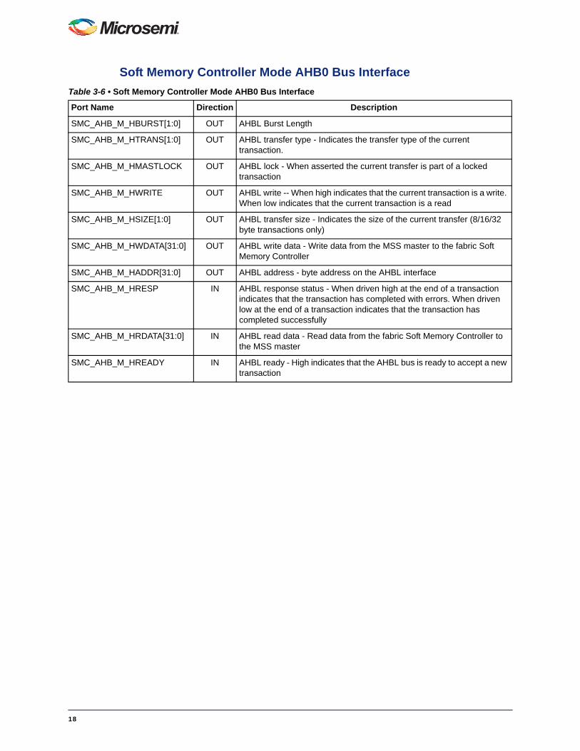
Soft Memory Controller Mode AHB0 Bus Interface
Table 3-6 • Soft Memory Controller Mode AHB0 Bus Interface
Port Name Direction Description
SMC_AHB_M_HBURST[1:0] OUT AHBL Burst Length
SMC_AHB_M_HTRANS[1:0] OUT AHBL transfer type - Indicates the transfer type of the current transaction.
SMC_AHB_M_HMASTLOCK OUT AHBL lock - When asserted the current transfer is part of a locked transaction
SMC_AHB_M_HWRITE OUT AHBL write -- When high indicates that the current transaction is a write. When low indicates that the current transaction is a read
SMC_AHB_M_HSIZE[1:0] OUT AHBL transfer size - Indicates the size of the current transfer (8/16/32 byte transactions only)
SMC_AHB_M_HWDATA[31:0] OUT AHBL write data - Write data from the MSS master to the fabric Soft Memory Controller
SMC_AHB_M_HADDR[31:0] OUT AHBL address - byte address on the AHBL interface
SMC_AHB_M_HRESP IN AHBL response status - When driven high at the end of a transaction indicates that the transaction has completed with errors. When driven low at the end of a transaction indicates that the transaction has completed successfully
SMC_AHB_M_HRDATA[31:0] IN AHBL read data - Read data from the fabric Soft Memory Controller to the MSS master
SMC_AHB_M_HREADY IN AHBL ready - High indicates that the AHBL bus is ready to accept a new transaction
18
A – Product Support
Microsemi SoC Products Group backs its products with various support services, including Customer Service, Customer Technical Support Center, a website, electronic mail, and worldwide sales offices. This appendix contains information about contacting Microsemi SoC Products Group and using these support services.
Customer ServiceContact Customer Service for non-technical product support, such as product pricing, product upgrades, update information, order status, and authorization.
From North America, call 800.262.1060From the rest of the world, call 650.318.4460Fax, from anywhere in the world, 408.643.6913
Customer Technical Support CenterMicrosemi SoC Products Group staffs its Customer Technical Support Center with highly skilled engineers who can help answer your hardware, software, and design questions about Microsemi SoC Products. The Customer Technical Support Center spends a great deal of time creating application notes, answers to common design cycle questions, documentation of known issues, and various FAQs. So, before you contact us, please visit our online resources. It is very likely we have already answered your questions.
Technical SupportVisit the Customer Support website (www.microsemi.com/soc/support/search/default.aspx) for more information and support. Many answers available on the searchable web resource include diagrams, illustrations, and links to other resources on the website.
WebsiteYou can browse a variety of technical and non-technical information on the SoC home page, at www.microsemi.com/soc.
Contacting the Customer Technical Support CenterHighly skilled engineers staff the Technical Support Center. The Technical Support Center can be contacted by email or through the Microsemi SoC Products Group website.
EmailYou can communicate your technical questions to our email address and receive answers back by email, fax, or phone. Also, if you have design problems, you can email your design files to receive assistance. We constantly monitor the email account throughout the day. When sending your request to us, please be sure to include your full name, company name, and your contact information for efficient processing of your request.
The technical support email address is [email protected].
19
MOWSaFa
Microsemi Corporation (NASDAQ: MSCC) offers a comprehensive portfolio of semiconductorsolutions for: aerospace, defense and security; enterprise and communications; and industrialand alternative energy markets. Products include high-performance, high-reliability analogand RF devices, mixed signal and RF integrated circuits, customizable SoCs, FPGAs, andcomplete subsystems. Microsemi is headquartered in Aliso Viejo, Calif. Learn more atwww.microsemi.com.
icrosemi Corporate Headquarters
My CasesMicrosemi SoC Products Group customers may submit and track technical cases online by going to My Cases.
Outside the U.S.Customers needing assistance outside the US time zones can either contact technical support via email ([email protected]) or contact a local sales office. Sales office listings can be found at www.microsemi.com/soc/company/contact/default.aspx.
ITAR Technical SupportFor technical support on RH and RT FPGAs that are regulated by International Traffic in Arms Regulations (ITAR), contact us via [email protected]. Alternatively, within My Cases, select Yes in the ITAR drop-down list. For a complete list of ITAR-regulated Microsemi FPGAs, visit the ITAR web page.
5-02-00377-2/06.14
© 2014 Microsemi Corporation. All rights reserved. Microsemi and the Microsemi logo are trademarks ofMicrosemi Corporation. All other trademarks and service marks are the property of their respective owners.
ne Enterprise, Aliso Viejo CA 92656 USAithin the USA: +1 (949) 380-6100les: +1 (949) 380-6136x: +1 (949) 215-4996