Embed Size (px)
Citation preview

Application Note AC428
SmartFusion2 and IGLOO2 - DDR Low Power Modes - Libero SoC v11.6
Table of Contents
PurposeThis application note describes the double-data rate (DDR) low power modes using an example designfor the IGLOO®2 field programmable gate array (FPGA) Evaluation Kit board. The DDR low powermodes explained in this application note can also be used for the SmartFusion®2 system-on-chip (SoC)FPGA devices.
IntroductionIn FPGA based designs, power consumption and design complexity are two significant factors. Achievingthe SoC functionality in an FPGA reduces the design complexity, yet power consumption is the mostcritical issue for the design community. The SmartFusion2 SoC FPGAs and IGLOO2 FPGAs reduce thedesign complexity and exhibit low power characteristics similar to an application specific integratedcircuit (ASIC), making the SmartFusion2 SoC FPGAs and IGLOO2 FPGAs an ideal choice for powersensitive applications. The DDR controllers in the SmartFusion2 and IGLOO2 devices support variouspower-saving modes to reduce the overall system power consumption.
Purpose . . . . . . . . . . . . . . . . . . . . . . . . . . . . . . . . . . . . . . . . . . . . . . . . . . 1Introduction . . . . . . . . . . . . . . . . . . . . . . . . . . . . . . . . . . . . . . . . . . . . . . . . 1References . . . . . . . . . . . . . . . . . . . . . . . . . . . . . . . . . . . . . . . . . . . . . . . . 2Design Requirements . . . . . . . . . . . . . . . . . . . . . . . . . . . . . . . . . . . . . . . . . . . 2
Power Saving Modes . . . . . . . . . . . . . . . . . . . . . . . . . . . . . . . . . . . . . . . . . . . 3Self-Refresh . . . . . . . . . . . . . . . . . . . . . . . . . . . . . . . . . . . . . . . . . . . . . . . . .3Precharge Power-Down . . . . . . . . . . . . . . . . . . . . . . . . . . . . . . . . . . . . . . . . . . .3Deep Power-Down (DPD) . . . . . . . . . . . . . . . . . . . . . . . . . . . . . . . . . . . . . . . . . .4Stop Clock . . . . . . . . . . . . . . . . . . . . . . . . . . . . . . . . . . . . . . . . . . . . . . . . . .4
Implementing Power Saving Modes on IGLOO2 Device . . . . . . . . . . . . . . . . . . . . . . . . . 4Design Description . . . . . . . . . . . . . . . . . . . . . . . . . . . . . . . . . . . . . . . . . . . . . .4Hardware Implementation . . . . . . . . . . . . . . . . . . . . . . . . . . . . . . . . . . . . . . . . . .8Configuring the System Builder . . . . . . . . . . . . . . . . . . . . . . . . . . . . . . . . . . . . . . .9Simulation using Microsemi LPDDR SDRAM VIP Model . . . . . . . . . . . . . . . . . . . . . . . . . 13Setting Up Simulation Model . . . . . . . . . . . . . . . . . . . . . . . . . . . . . . . . . . . . . . . . 14Running the Design . . . . . . . . . . . . . . . . . . . . . . . . . . . . . . . . . . . . . . . . . . . . 20Setting Up the Hardware . . . . . . . . . . . . . . . . . . . . . . . . . . . . . . . . . . . . . . . . . . 20IGLOO2 LPDDR Power Modes GUI . . . . . . . . . . . . . . . . . . . . . . . . . . . . . . . . . . . . 21Power Measurements . . . . . . . . . . . . . . . . . . . . . . . . . . . . . . . . . . . . . . . . . . . 24
Conclusion . . . . . . . . . . . . . . . . . . . . . . . . . . . . . . . . . . . . . . . . . . . . . . . 26
Appendix A: Design Files . . . . . . . . . . . . . . . . . . . . . . . . . . . . . . . . . . . . . . . . 27
Appendix B: Changing LPDDRI to LVCMOS18 I/O Type . . . . . . . . . . . . . . . . . . . . . . . . 28Libero SoC . . . . . . . . . . . . . . . . . . . . . . . . . . . . . . . . . . . . . . . . . . . . . . . . . 28IGLOO2 Evaluation Kit Board . . . . . . . . . . . . . . . . . . . . . . . . . . . . . . . . . . . . . . . 29
List of Changes . . . . . . . . . . . . . . . . . . . . . . . . . . . . . . . . . . . . . . . . . . . . . 30
Supers
eded
September 2015 1
© 2015 Microsemi Corporation

SmartFusion2 and IGLOO2 - DDR Low Power Modes - Libero SoC v11.6
The DDR controllers can operate the DDR memories in the following power saving modes:
• Self-Refresh
• Precharge power-down (PPD)
• Deep power-down (DPD)
• Stop clock
The example design describes how to implement the power saving modes on the IGLOO2 Evaluation Kitboard. The example design package has a graphical user interface (GUI) that runs on a host PC tocommunicate with the IGLOO2 Evaluation Kit board. The GUI allows enabling or disabling the powersaving modes, start or stop, and read or write transactions to the DDR memories.
The example design has
• Advanced eXtensible Interface (AXI) master
• Advanced High Performance Bus Lite (AHBL) master
• Command decoder
• CoreUART interface logic
The CoreUART interface logic receives the commands from the GUI and sends them to the Commanddecoder. The Command decoder decodes the commands and generates the AXI write or read signals,and the AHBL write or read signals.
To indicate the memory write or read operation, a graph is displayed on the GUI. The power savingoptions in the GUI trigger the AHBL write transaction, which enables or disables the power saving mode.The core power and power across LPDDR memory are measured during the low power modes andmemory operation.
ReferencesThe list of references are:
• UG0446: SmartFusion2 and IGLOO2 FPGA High Speed DDR Interfaces User Guide
• AC409:Connecting User Logic to AXI Interfaces of High-Perf Comm Blocks-SmartFusion2
• AC333: Connecting User Logic to the SmartFusion Microcontroller Subsystem Application Note
• SmartFusion2 DDR Controller and Serial High Speed Controller Initialization Methodology
• UG0478: IGLOO2 FPGA Evaluation Kit User Guide
• IGLOO2 System Builder User Guide
Design RequirementsTable 1 lists the design requirements.
Table 1 • Design Requirements
Design Requirements Description
Hardware Requirements
IGLOO2 Evaluation Kit Rev C or later
Desktop or Laptop Any 64-bit Windows Operating System
Software Requirements
Libero® System-on-Chip (SoC) v11.6
FlashPro4 Programming Interface v11.6
Microsoft .NET Framework 4 Client Profile –
Supers
eded
2

Power Saving Modes
Power Saving ModesThe DDR controllers in the SmartFusion2 and IGLOO2 devices support various power-saving modes toreduce the overall system power consumption. This section describes the following power saving modes:
• Self-Refresh
• Precharge Power-Down
• Deep Power-Down (DPD)
• Stop Clock
Enabling and Disabling Power Saving ModesThe following methods describe how to enable or disable DDR Low Power Modes:
• An AHB/advanced peripheral bus 3 (APB) master in the FPGA fabric accesses themicrocontroller subsystem double-data rate (MDDR) configuration registers to enable or disabledthe DDR low power modes.
• DDR low power mode can be enabled or disabled while configuring the System Builder. Navigateto the Memories page > Memory Initialization in the System Builder MDDR Configurator GUI.
Self-RefreshThe self-refresh mode is used to retain the data without an external clocking in the DDR memory whilethe rest of the system is powered down. An internal temperature sensor in the DDR memory adjusts therefresh rate to optimize the device power consumption while ensuring the data integrity. During self-refresh, the refresh intervals are scheduled internally, and vary from the specified average periodicrefresh interval (REFI) time entered in the DDR configurator GUI.
The DDR controller puts the DDR memory devices in self-refresh mode.This is when the
• REG_DDRC_SELFREF_EN register bit is set
• There are no read or write operations pending in the DDR controller
The DDR controller forces the DDR memory out of self-refresh mode, when theREG_DDRC_SELFREF_EN input is de-asserted or new commands are received.
To demonstrate the different low power modes, an AHB master in the FPGA fabric accesses the MDDRconfiguration registers to enable or disabled the self-refresh mode as described in the example design,refer to Table 2 on page 7. Based on the design requirements, the self-refresh mode can be enabled ordisabled while configuring the System Builder. Navigate to the Memories Tab > Memory Initialization inthe System Builder MDDR Configurator GUI to enable or disable the self-refresh mode.
Precharge Power-DownIf REG_DDRC_POWERDOWN_EN = 1, the DDR controller automatically changes the DDR memory tothe precharge power-down mode after the period specified in the REG_DDRC_POWERDOWN_TO_X32register. Entering into the precharge power-down mode deactivates all the DDR I/Os, except clockenable (CKE).
The DDR controller automatically performs the precharge power-down exit on any of the followingconditions:
• A refresh cycle is required to any rank in the system.
• The DDR controller receives a new request from the core logic.
• REG_DDRC_POWERDOWN_EN bit is set to 0.
The precharge power-down mode can be enabled or disabled while configuring the System Builder.Navigate to the Memories Tab > Memory Initialization > Powerdown Enabled in the System BuilderMDDR Configurator GUI.
Supers
eded
3

SmartFusion2 and IGLOO2 - DDR Low Power Modes - Libero SoC v11.6
Deep Power-Down (DPD)The DPD mode is supported only for LPDDR1. The DPD mode minimizes the memory powerconsumption by shutting down the internal power to the memory array, and stopping the refreshoperations. Data is not retained if the device changes to the DPD mode. The DPD mode is effectivewhen the LPDDR SDRAM devices are not accessed and data retention is not required.
The DDR controller changes the LPDDR SDRAM devices to the DPD mode
• If the REG_DDRC_DEEPPOWERDOWN_EN bit is set
• There are no read or write operations pending in the DDR controller
The DDR controller automatically exits the DPD mode and runs the initialization sequence again, whenthe REG_DDRC_DEEPPOWERDOWN_EN bit is reset to 0.
Based on the design requirements, the DPD mode can be enabled or disabled while configuring theSystem Builder. Navigate to the Memories Tab > Memory Initialization > Deep Power-down Enabled in the System Builder MDDR Configurator GUI.
Stop ClockA method of minimizing the memory power consumption is to stop the DDR SDRAM clock. The stopclock mode is supported only for LPDDR1. Stop the DDR SDRAM clock, when the LPDDR SDRAMdevices are not accessed. All the SDRAM operations must be completed before entering into the stopclock mode.
The DDR controller stops the DDR clock
• When the REG_DDRC_CLOCK_STOP_EN bit is set
• There are no read or write operations pending in the DDR controller
The DDR controller exits the stop clock mode, when the REG_DDRC_CLOCK_STOP_EN bit is reset to0.
The stop clock mode can be enabled or disabled while configuring the System Builder. Navigate to theMemories Tab > Memory Initialization > Stop Clock in the System Builder MDDR Configurator GUI.
Implementing Power Saving Modes on IGLOO2 Device Power saving modes such as self-refresh, precharge power-down, DPD, and stop clock are implementedand validated using the IGLOO2 Evaluation Kit board. This section describes the following:
• Design Description
• Hardware Implementation
• Running the Design
Design DescriptionThe example design has the following:
• HPMS - System Builder Generated
• DDR initialization subsystem - System Builder Generated
• AXI master (AXI_IF)
• AHBL master (AHB_IF)
• Command decoder (CMD_Decoder)
• COM interface (COM_Interface) block
Supers
eded
4

Implementing Power Saving Modes on IGLOO2 Device
Figure 1 shows the IGLOO2 top-level block diagram.
The System Builder is used to create high performance memory subsystem (HPMS) with the MDDR andDDR initialization subsystems. The memory subsystem double-data rate (MDDR) in HPMS is configuredto use the LPDDR interface. The AXI interface in the DDR FIC subsystem routed to the FPGA fabric.
The DDR initialization subsystem has the CoreConfigMaster and CoreConfigP IPs that initialize theMDDR controller.
The following steps describe how to initialize the process:
1. The CoreConfigMaster IP (AHBL Master) accesses the DDR configuration data that is stored ineNVM using the FIC_0 port.
2. The configuration data is sent to the CoreConfigP IP using the FIC_2 master port.
3. The CoreConfigP IP sends the configuration data to the APB bus of MDDR.
Figure 1 • IGLOO2 Top-Level Block Diagram
Supers
eded
5
SmartFusion2 and IGLOO2 - DDR Low Power Modes - Libero SoC v11.6
The Command decoder receives the command from the COM interface block and generates thefollowing signals:
• AXI write start
• AXI read start
• AXI write data size
• AXI read data size
• AHB write
• AHB read
• AHB address
• AHB write data
The AXI write size and read size are fixed to 2 KB. Figure 2 shows the command decoding.
Command [5:2] is used to decode the request for enabling or disabling the low power mode and readingthe status register. The Command decoder generates the AHB write, AHB read, AHB Address, and AHBwrite data signals to write or read from the MDDR configuration register.
Figure 2 • Command DecodingSupers
eded
6

Implementing Power Saving Modes on IGLOO2 Device
Table 2 lists the MDDR configuration registers that are used for implementing the low power modes.
Refer to UG0446: SmartFusion2 and IGLOO2 FPGA High Speed DDR Interfaces User Guide for moreinformation.
The AHBL master handles the MDDR configuration register transaction request from the Commanddecoder. The output of the AHBL master is connected to the COM interface block. The AHBL mastersends the MDDR register values to the COM interface block for a read transaction request. The controllogic in the COM interface block reads the values and sends to the host PC using the CoreUARTinterface.
The AXI master block has
• AXI read channel
• AXI write channel
• write throughput counter
• read throughput counter
• 512 x 64 LSRAM
It performs the write or read operation1 based on the input signals from the Command decoder. Duringthe write operation, the AXI master reads from the LSRAM and writes to the LPDDR memory, and thenmeasures the write throughput. During the read operation, the AXI master reads from the LPDDRmemory and writes to the LSRAM, and then measures the read throughput. The write throughput countercounts the AXI clocks between AWVALID of first data and WLAST of last data. Similarly, the readthroughput counter counts the AXI clocks between ARVALID of first data and RLAST of last data.
After triggering the write or read operation, the AXI master performs the write or read operation eighttimes to get the average throughput and ACTIVATE all banks. During the write operation, the writeaddress (AWADDR) starts from 0x00000000, incremented by 128 (16-beat burst). During the readoperation, the read address (ARADDR) starts from 0x00000000, incremented by 128.
After each write or read operation, the AXI master sends the throughput count value and an addressstarting from 0x0 to the COM interface block. Then, the COM interface block writes the throughput valuesinto TPSRAM. The control logic in the COM interface block reads the values and sends to the host PCusing the CoreUART interface.
Note: This application note re-uses the design from Optimizing DDR Controller for Improved Efficiencyapplication note to implement the continuous write and read memory operation. This application note is focused on low power modes and therefore the throughput values are notvalidated. It is recommended to refer the following application notes to understand the throughputmeasurement and MDDR controller optimization techniques:
– AC422: SmartFusion2 - Optimizing DDR Controller for Improved Efficiency
– AC424: IGLOO2 - Optimizing DDR Controller for Improved Efficiency
Table 2 • MDDR Configuration Registers
Low Power Mode Register NameAddressOffset Data
Stop clock DDRC_PWR_SAVE_1_CR 0×084 0x414 - Disables the stop clock
0x415 - Enables the stop clock
Self-refresh DDRC_DYN_REFRESH_1_CR 0×008 0xc88 - Disables the self-refresh
0xca8 - Enables the self-refresh
Precharge Power Down and Deep Power Down
DDRC_DYN_POWERDOWN_CR 0×010 0x0 - Disables PPD and DPD
0x1 - Disables PPD and enables DPD
0x2 - Enables PPD and disables DPD
0x3 - Enables PPD and DPD
1. One AXI write or read operation equals to 16x16-beat burst (16x16x64).
Supers
eded
7
SmartFusion2 and IGLOO2 - DDR Low Power Modes - Libero SoC v11.6
For information about Creating a Custom AXI Interface on User Logic in SmartFusion2, refer toAC409:Connecting User Logic to AXI Interfaces of High-Perf Comm Blocks-SmartFusion2.
For information about Creating a Custom AHB Interface on User Logic, refer to AC333: Connecting UserLogic to the SmartFusion Microcontroller Subsystem Application Note
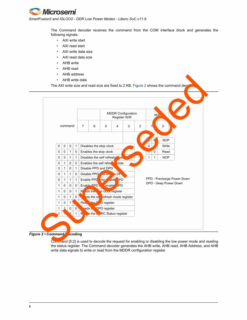
Hardware ImplementationThe hardware implementation has the following:
• Configuring the System Builder wizard.
• Connecting with the custom logic (AXI master, AHBL master, Command decoder and COMinterface).
Figure 3 shows the IGLOO2 top-level SmartDesign.
Figure 3 • IGLOO2 Top-Level SmartDesign
Supers
eded
8

Implementing Power Saving Modes on IGLOO2 Device
Configuring the System BuilderThis section describes how to configure MDDR and other device features, and build a complete systemusing the System Builder graphical design wizard in the Libero SoC software. Refer to the IGLOO2System Builder User Guide for more information about how to launch the System Builder wizard and itsusages.
The follow steps describe how to configure the MDDR subsystem and access it from the AXI master inthe FPGA fabric:
1. Launch the Libero SoC software and System Builder.
2. Click the Device Features tab in the System Builder window. Figure 4 shows the SystemBuilder - Device Features window.
3. Select the HPMS External Memory and HPMS On-Chip SRAM (eSRAM) check boxes underMemory as shown in Figure 4.
4. Click the Memories tab. The System Builder-Memories window is displayed as shown inFigure 5 on page 10.
Figure 4 • System Builder - Device Features Supers
eded
9

SmartFusion2 and IGLOO2 - DDR Low Power Modes - Libero SoC v11.6
In this example, the design is created to access the LPDDR memory with a 16-bit data width andno ECC.
5. Set the DDR memory settling time (us) as 200.
6. Click Import Configuration to initialize the DDR memory. The configuration file is stored ineNVM. The MDDR subsystem registers should be initialized before accessing the DDR memorythrough the MDDR subsystem. The MDDR configuration register file is provided along with thedesign file. Refer to "Appendix A: Design Files" on page 27 for more information.
Figure 5 • System Builder - Memories
Supers
eded
10

Implementing Power Saving Modes on IGLOO2 Device
7. Click the Peripherals tab. The System Builder-Peripherals window is displayed as shown inFigure 6.
8. Drag-and-drop Fabric AMBA Master from the bottom left pane to the HPMS DDR FICSubsystem on the right pane. The AMBA_MASTER_0 is added to the subsystem and configuredthe Interface Type as an AXI.
Note: The HPMS_FIC_0_USER_MASTER is added to the HPMS FIC_0 - Fabric Master Subsystem bydefault. It enables the AHBL master in the FPGA fabric to connect to the FIC_0 subsystem andaccess the MDDR configuration registers.
Figure 6 • System Builder - Peripherals
Supers
eded
11

SmartFusion2 and IGLOO2 - DDR Low Power Modes - Libero SoC v11.6
9. Click the Clocks tab. The Clock window is displayed as shown in Figure 7.
10. Configure the System Clock and Subsystem Clocks in the Clocks tab as listed in Table 3.
11. Follow the rest of the steps with the default settings and generate the design.
12. Instantiate the custom logic for AXI master, AHBL master, Command decoder, and COM interfaceto make the connections as shown in Figure 3 on page 8.
Figure 7 • System and Subsystem Clocks Configuration
Table 3 • System and Subsystem Clocks
Clock Name Frequency (MHz)
System Clock On-chip 25 MHz/50 MHz RC Oscillator
HPMS_CLK 83
MDDR_CLK 166
DDR/SMC_FIC_CLK 83
FIC_0_CLK 83Supers
eded
12

Implementing Power Saving Modes on IGLOO2 Device
Figure 8 shows the SmartDesign of the COM Interface Block. The COM_interface SmartDesign does theUART communication between the GUI and AXI or AHBL master logic.
The COREUART_0 IP receives the UART signals from the GUI. The Control_Logic_0 collects the reador write command from the COREUART_0 and sends it to the AXI master using the Command decoder,which triggers the read or write operation. After the write or read operation, the Control_Logic_0 readsthe throughput count values from TPSRAM_0 and sends them to the host PC using the COREUART_0IP. Similarly, the Control_Logic_0 collects the power saving mode commands from the COREUART_0 IPand sends them to the AHBL master using the Command decoder, which enables or disables the powersaving mode.
CoreUART IP has the following configuration:
• Baud Rate: 115200
• Data Bits: 8
• Parity: None
TPSRAM IP has the following configuration:
• Write port depth: 8
• Write port width: 16
• Read port depth: 16
• Read port width: 8
Simulation using Microsemi LPDDR SDRAM VIP ModelThe Libero SoC includes a generic DDR memory simulation model, also called verification intellectualproperty (VIP). This VIP is attached to the pin side of the MDDR or fabric double-data rate (FDDR)subsystem, and it simulates the functionality of a DDR memory device. It can also be configured forDDR2, DDR3, and LPDDR SDRAM memories.
Figure 8 • SmartDesign - COM Interface Block Diagram
Supers
eded
13

SmartFusion2 and IGLOO2 - DDR Low Power Modes - Libero SoC v11.6
Setting Up Simulation ModelThe following steps describe how to set up and run the simulation:
1. Click the Catalog tab in the Libero SoC.
2. Select the Simulation Mode check box.
3. Select the Generic DDR Memory Simulation model under Memory & Controllers to drag intothe SmartDesign testbench canvas. Figure 9 shows the Catalog dialog box.
Figure 9 • Catalog Dialog Box
Supers
eded
14

Implementing Power Saving Modes on IGLOO2 Device
The example design uses an instance of SimDRAM (VIP model) with 16 data width.
Figure 10 • Configuring SimDRAM_0
Supers
eded
15
SmartFusion2 and IGLOO2 - DDR Low Power Modes - Libero SoC v11.6
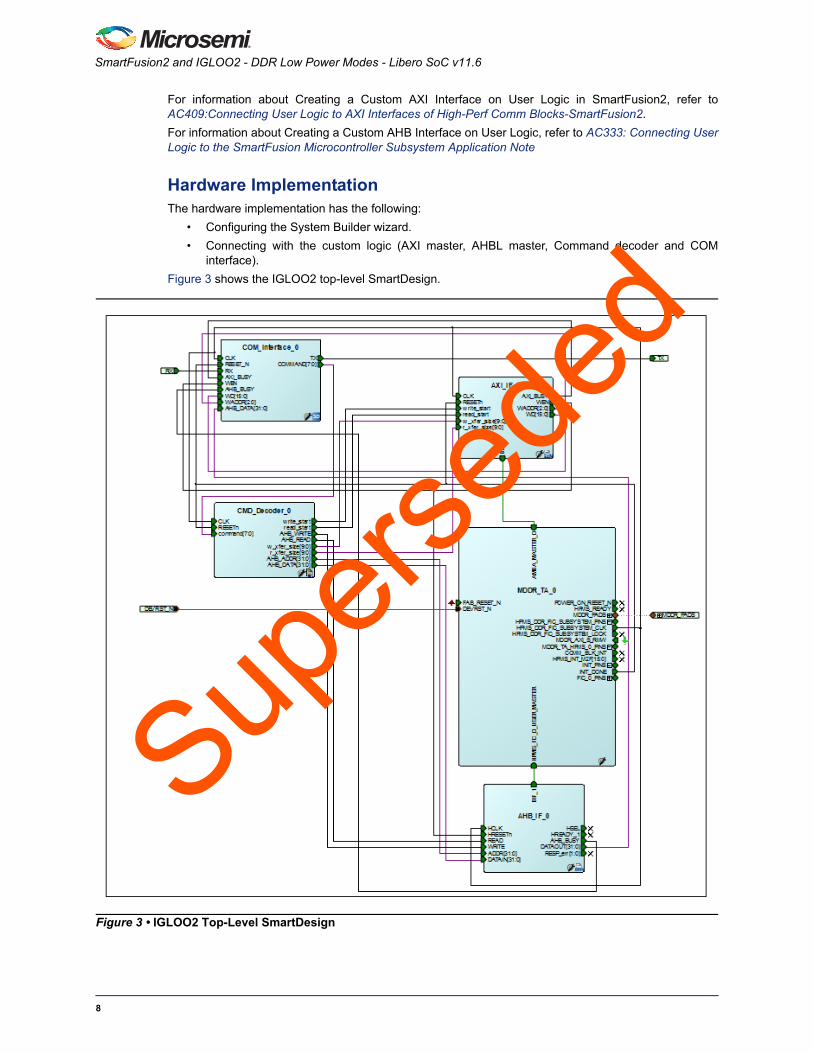
4. Connect the signals as shown in Figure 11.
5. Click SmartDesign > Generate Component to generate the design or click the GenerateComponent icon on the SmartDesign tool bar.
6. Click the Files tab. Figure 12 shows the folder structure in Files window.
7. Navigate to Component > Work > LPDDRP_VIP_Simulation folders in Files window.
8. Double-click LPDDR_VIP_Simulation.v to open the generated SmartDesign testbench file.Figure 12 shows the SmartDesign generated testbench file.
9. Replace timescale 1ns/100ps with timescale 1ps/1fs.
Figure 11 • SmartDesign Testbench for Example Design with Microsemi LPDDR SDRAM VIP
Figure 12 • SmartDesign Generated Testbench File
Supers
eded
16

Implementing Power Saving Modes on IGLOO2 Device
10. Add the following code above endmodule:
wire MDDR_CLK;wire MDDR_CKE;wire MDDR_CS_N;wire [15:0] MDDR_ADDR;wire [2:0] MDDR_BA;
wire [7:0] TX_DATA;wire [1:0] MDDR_DM_RDQS;wire [15:0] MDDR_DQ;wire [1:0] MDDR_DQS;wire [2:0] COMMAND;reg txdata;
reg BRCLK;parameter BRCLK_PERIOD = 8680500; /* COREUART BAUD RATE 115200 Hz */
assign MDDR_DM_RDQS = net_2;assign MDDR_DQ = net_1;assign MDDR_DQS = net_0;assign MDDR_CLK = MDDR_TA_top_0_MDDR_CLK;assign MDDR_CKE = MDDR_TA_top_0_MDDR_CKE;assign MDDR_CS_N = MDDR_TA_top_0_MDDR_CS_N;assign MDDR_ADDR = MDDR_TA_top_0_MDDR_ADDR;assign MDDR_BA = MDDR_TA_top_0_MDDR_BA;
assign COMMAND = {MDDR_TA_top_0_MDDR_RAS_N,MDDR_TA_top_0_MDDR_CAS_N,MDDR_TA_top_0_MDDR_WE_N};assign TX_DATA = LPDDR_VIP_Simulation.MDDR_TA_top_0.COM_Interface_0.COREUART_0.DATA_IN;
initialbegin
BRCLK = 1'b0; @(posedge LPDDR_VIP_Simulation.MDDR_TA_top_0.AXI_IF_0.CLK); repeat(3000) begin #(BRCLK_PERIOD / 2.0) BRCLK <= !BRCLK; end
end
initialbegin $display ("+++++++++++++++++++++++++++++++++++++++++++++++++++++++++++++"); $display ("Loading LSRAM from lsram.mem file"); $display (""); $readmemh("lsram_512x64.mem",LPDDR_VIP_Simulation.MDDR_TA_top_0.AXI_IF_0.Rdata_mem); $display (" Completed Loading LSRAM"); $display ("+++++++++++++++++++++++++++++++++++++++++++++++++++++++++++++");
@(posedge LPDDR_VIP_Simulation.MDDR_TA_top_0.AXI_IF_0.RESETn);
force LPDDR_VIP_Simulation.MDDR_TA_top_0.COM_Interface_0.COREUART_0.DATA_OUT = 8'b01_1110_00; /* Handshaking Command 'x' */@(posedge txdata ) /* Waiting for acknowledgement 'a' */repeat(1) @(posedge BRCLK);force LPDDR_VIP_Simulation.MDDR_TA_top_0.COM_Interface_0.COREUART_0.DATA_OUT = 8'b00_0000_01; /* Write command */ repeat(10) @(posedge BRCLK);
Supers
eded
17

SmartFusion2 and IGLOO2 - DDR Low Power Modes - Libero SoC v11.6
force LPDDR_VIP_Simulation.MDDR_TA_top_0.COM_Interface_0.COREUART_0.DATA_OUT = 8'b00_1000_00; /* DEEP POWER DOWN Entry */ repeat(10) @(posedge BRCLK);
force LPDDR_VIP_Simulation.MDDR_TA_top_0.COM_Interface_0.COREUART_0.DATA_OUT = 8'b00_0101_10; /* DEEP POWER DOWN Exit and Read */repeat(10) @(posedge BRCLK);
force LPDDR_VIP_Simulation.MDDR_TA_top_0.COM_Interface_0.COREUART_0.DATA_OUT = 8'b00_0000_00; /* NO OPERATION */
end
always @(posedge LPDDR_VIP_Simulation.MDDR_TA_top_0.AXI_IF_0.CLK)begin if(TX_DATA == 8'b01100001) begin txdata <= 1'b1; end else begin txdata <= 1'b0; endend
11. Click the Stimulus Hierarchy tab. Figure 13 shows the Stimulus Hierarchy window.
12. Right-click LPDDR_VIP_Simulation and select Set as active stimulus to set the SmartDesigntestbench as active stimulus. Figure 13 shows the Stimulus Hierarchy window.
Figure 13 • Stimulus Hierarchy
Supers
eded
18
Implementing Power Saving Modes on IGLOO2 Device
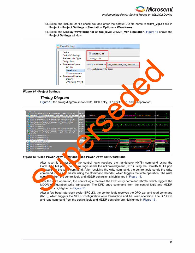
13. Select the Include Do file check box and enter the default DO file name to wave_vip.do file inProject > Project Settings > Simulation Options > Waveforms.
14. Select the Display waveforms for as top_level LPDDR_VIP Simulation. Figure 14 shows theProject Settings window.
Timing DiagramFigure 15 the timing diagram shows write, DPD entry, DPD exit, read, and no operation.
After reset is de-asserted, the control logic receives the handshake (0x78) command using theCoreUART RX port. The control logic sends the acknowledgment (0x61) using the CoreUART TX portand waits for the write command. After receiving the write command, the control logic sends the writecommand to the AXI master using the Command decoder, which triggers the write operation. The writecommand from the control logic and MDDR controller is highlighted in Figure 15.
After the write operation, the control logic receives the DPD entry command (0x20), which triggers theMDDR configuration write transaction. The DPD entry command from the control logic and MDDRcontroller is highlighted in Figure 15.
After a few baud rate clock cycle (BRCLK), the control logic receives the DPD exit and read command(0x16), which triggers the MDDR configuration write transaction and AXI read operation. The DPD exitand read command from the control logic and MDDR controller are highlighted in Figure 15.
Figure 14 • Project Settings
Figure 15 • Deep Power-Down Entry and Deep Power-Down Exit Operations
Supers
eded
19

SmartFusion2 and IGLOO2 - DDR Low Power Modes - Libero SoC v11.6
Running the DesignThe example design is designed to run on the IGLOO2 Evaluation Kit board. Refer to the IGLOO2-Evaluation Kit for more information.
Setting Up the HardwareThe following steps describe how to setup the hardware:
1. Connect the jumpers on the IGLOO2 Evaluation Kit board as listed in Table 4.
Note: Ensure that the power supply switch, SW7 is switched off when connecting the jumpers.
2. Connect the Power supply to the J6 connector.
3. Switch on the power supply switch, SW7.
4. Connect the FlashPro4 programmer to the PROG HEADER J5 connector of the IGLOO2Evaluation Kit board.
5. Connect the host PC USB port to the IGLOO2 Evaluation Kit board's J18 (FTDI) USB connectorusing the USB mini-B cable.
6. Ensure that the USB to UART bridge drivers are automatically detected. This can be verified in the Device Manager of the host PC. If the USB to UART bridge drivers are not installed, download the drivers from www.microsemi.com/soc/documents/CDM_2.08.24_WHQL_Certified.zip.
7. Program the IGLOO2 Evaluation Kit board with the generated or provided *.stp file (Refer to"Appendix A: Design Files" on page 27) using FlashPro4.
Table 4 • IGLOO2 FPGA Evaluation Kit Jumper Settings
Jumpers Pin (from) Pin (to) Comments
J22 1 2 Default
J23 1 2 Default
J24 1 2 Default
J8 1 2 Default
J3 1 2 Default
Supers
eded
20

Implementing Power Saving Modes on IGLOO2 Device
IGLOO2 LPDDR Power Modes GUIThe example design has a Windows GUI and IGL2_LPDDR_LP.exe that run on the host PC tocommunicate with the IGLOO2 Evaluation Kit board. The UART protocol is used as a communicationprotocol between the host PC and IGLOO2 Evaluation Kit board. Figure 16 shows the initial screen of theGUI.
The following steps describe the functionalities of LPDDR Power Modes:
1. Click the Power Modes tab. The Power Modes window is displayed as shown in Figure 16.
2. Select Write or Read under Transfer Type.
3. Select the following Power Modes check boxes as required:
– Stop Clock
– Self Refresh
– Power Down (Precharge Power-Down)
– Deep Power-Down
4. Click R to read back the content of MDDR Configuration Registers. The Status Registerdisplays the current operational mode on the right pane of the GUI as shown in Figure 16.
Power modes and their purposes,
– Connect: connects or disconnects the serial port communication between the host PC andthe IGLOO2 Evaluation Kit board.
– Start: starts or stops the write or read operation.
– Enable Graph: starts or stops plotting the throughput values.
– Exit: quits the application.
5. Run the IGLOO2 LPDDR power modes .exe and launch the GUI. The default location is at <download_folder>\m2s_m2gl_ac428_ddrlowpwr_liberov11p6_df/M2S_M2GL_AC428_DF/Windows_Utility\IGL2_LPDDR_LP.exe
Figure 16 • IGLOO2 LPDDR Power Modes
Supers
eded
21

SmartFusion2 and IGLOO2 - DDR Low Power Modes - Libero SoC v11.6
6. Click Connect and wait until it connects to the FDTI COM port. The connection status along withthe COM port and baud rate is displayed in the left bottom corner of the window. Figure 17 showsthe connection status and baud rate.
7. Click R one-by-one. The MDDR Configuration Registers content is displayed in the text boxes.The Status Register displays the current operational mode. Figure 18 shows the MDDRConfiguration Registers.
8. Select the Power Down check box under Power Modes. The LPDDR (or MDDR) memorychanges to the power down mode.
Figure 17 • IGLOO2 LPDDR Power Modes Connection Status
Figure 18 • MDDR Configuration Registers
Supers
eded
22

Implementing Power Saving Modes on IGLOO2 Device
9. Click Status Register R. Figure 19 shows the power down mode.
10. Click Start as highlighted in Figure 19. It triggers the LPDDR memory write operation after exitingthe power down mode.
11. Click Status Register R. Figure 20 shows the normal mode after exiting the power down mode.
Figure 19 • Power-Down Mode
Figure 20 • Normal Mode after Exiting Power Down Mode
Supers
eded
23

SmartFusion2 and IGLOO2 - DDR Low Power Modes - Libero SoC v11.6
12. Click Enable Graph as highlighted in Figure 20 on page 23. Figure 21 shows the moving graph of a write or read operation.
Power MeasurementsThe LPDDR memory is connected to 1.8 V voltage rail in the IGLOO2 Evaluation Kit board. The 1.8 Vvoltage rail is also shared by other components such as USB PHY, Ethernet PHY, and so on. Therefore,the exact power measurement is not possible during low power modes. However, the power variationscan be co-related with the low power modes.
The LVCMOS18 I/O standard has lower power characteristics for LPDDR memories than the LPDDRI(SSTL18) standard. The IGLOO2 Evaluation Kit board and design example use the LPDDRI type I/Os.Change the I/O type in the example design to LVCMOS18 and re-work on the board to observe thelowest power characteristics. To change the I/O type in the example design and IGLOO2 Evaluation Kitboard, refer to "Appendix B: Changing LPDDRI to LVCMOS18 I/O Type" on page 28.
The IGLOO2 Evaluation Kit board has a voltage measuring circuit, which measures the voltage acrossthe 1.8 V voltage rail current sense resistor.
EQ 1 The power is calculated using the following equation:
Current (mA) = Measured Voltage (mV) ÷ 5 (Scaling Factor)
Power (mW) = 1.8 × Current
Figure 21 • Graph
Supers
eded
24

Implementing Power Saving Modes on IGLOO2 Device
Figure 22 shows the IGLOO2 Evaluation Kit board.
To measure the voltage across the 1.8 V voltage rail current sense resistor;
Connect the positive terminal of a standard digital voltmeter (DVM)/multimeter to TP15 and negativeterminal to TP11. TP14 and TP7 terminals are used for measuring the core power.
Figure 23 shows that Stop Clock + Self Refresh has the lowest power.
Figure 22 • IGLOO2 Evaluation Kit Board
TP14
TP7
TP14
TP11
Figure 23 • Low Power Mode Characteristics
Supers
eded
25

SmartFusion2 and IGLOO2 - DDR Low Power Modes - Libero SoC v11.6
ConclusionThis application note describes the DDR low power modes using an example design for the IGLOO2Evaluation Kit board. It also shows the LPDDR SDRAM simulation flow using the Microsemi® LPDDRSDRAM VIP model. The DDR low power modes explained for the IGLOO2 device can be used for theSmartFusion2 device.
Supers
eded
26

Appendix A: Design Files
Appendix A: Design FilesDownload the design files from the Microsemi SoC Products Group website:
www.microsemi.com/soc/download/rsc/?f=m2s_m2gl_ac428_ddrlowpwr_liberov11p6_df
The design file consists of Libero SoC Verilog project, MDDR Configuration files, Simulation model files,and programming files (*.stp) for the IGLOO2 Evaluation Kit board. Refer to the readme.txt file includedin the design file for the directory structure and description.
Supers
eded
27

SmartFusion2 and IGLOO2 - DDR Low Power Modes - Libero SoC v11.6
Appendix B: Changing LPDDRI to LVCMOS18 I/O Type
Libero SoC In Memories tab, select I/O Standard > LVCMOS18 (Lowest Power) while configuring the SystemBuilder. Figure 24 shows the System Builder - Memories window.
Figure 24 • System Builder - Memories Tab with LVCMOS18 I/O Type Selected
Supers
eded
28

Appendix B: Changing LPDDRI to LVCMOS18 I/O Type
IGLOO2 Evaluation Kit BoardRemove the resistors and capacitors shown in Figure 25.
Figure 25 • LPDDR Termination Resistors
Supers
eded
29

SmartFusion2 and IGLOO2 - DDR Low Power Modes - Libero SoC v11.6
List of ChangesThe following table shows important changes made in this document for each revision.
Revision* Changes Page
Revision 2(September 2015)
Updated the document for Libero SoC v11.6 software release (SAR 71309). NA
Removed Appendix C: Characterization Report for Low Power Modes (SAR 69065). NA
Revision 1(February 2015)
Initial Release. NA
Note: *The revision number is located in the part number after the hyphen. The part number is displayed at the bottomof the last page of the document. The digits following the slash indicate the month and year of publication.
Supers
eded
30

51900296-2/09.15
Microsemi Corporate HeadquartersOne Enterprise, Aliso Viejo,CA 92656 USA
Within the USA: +1 (800) 713-4113 Outside the USA: +1 (949) 380-6100Sales: +1 (949) 380-6136Fax: +1 (949) 215-4996
E-mail: [email protected]
Microsemi Corporation (Nasdaq: MSCC) offers a comprehensive portfolio of semiconductorand system solutions for communications, defense & security, aerospace and industrialmarkets. Products include high-performance and radiation-hardened analog mixed-signalintegrated circuits, FPGAs, SoCs and ASICs; power management products; timing andsynchronization devices and precise time solutions, setting the world’s standard for time; voiceprocessing devices; RF solutions; discrete components; security technologies and scalableanti-tamper products; Ethernet Solutions; Power-over-Ethernet ICs and midspans; as well ascustom design capabilities and services. Microsemi is headquartered in Aliso Viejo, Calif., andhas approximately 3,600 employees globally. Learn more at www.microsemi.com.
© 2015 Microsemi Corporation. Allrights reserved. Microsemi and theMicrosemi logo are trademarks ofMicrosemi Corporation. All othertrademarks and service marks are theproperty of their respective owners.
Microsemi makes no warranty, representation, or guarantee regarding the information contained herein orthe suitability of its products and services for any particular purpose, nor does Microsemi assume anyliability whatsoever arising out of the application or use of any product or circuit. The products soldhereunder and any other products sold by Microsemi have been subject to limited testing and should notbe used in conjunction with mission-critical equipment or applications. Any performance specifications arebelieved to be reliable but are not verified, and Buyer must conduct and complete all performance andother testing of the products, alone and together with, or installed in, any end-products. Buyer shall not relyon any data and performance specifications or parameters provided by Microsemi. It is the Buyer'sresponsibility to independently determine suitability of any products and to test and verify the same. Theinformation provided by Microsemi hereunder is provided "as is, where is" and with all faults, and the entirerisk associated with such information is entirely with the Buyer. Microsemi does not grant, explicitly orimplicitly, to any party any patent rights, licenses, or any other IP rights, whether with regard to suchinformation itself or anything described by such information. Information provided in this document isproprietary to Microsemi, and Microsemi reserves the right to make any changes to the information in thisdocument or to any products and services at any time without notice.
Supers
eded