Embed Size (px)
Citation preview
6
5
4
1
2
3
IN+
IN-
GND
VDD
OUTH
OUTL
UCC27511
R1
R2
Q1
IN+
D1
C1
+
VOUT
VSOURCE
L1
C2
V+
4.5 V to 18 V
Noninverting Input
6
5
4
1
2
3
IN+
IN-
GND
VDD
OUTH
OUTL
UCC27511
R1
R2
Q1
IN-
D1
C1
+
VOUT
VSOURCE
L1
C2
V+
4.5 V to 18 V
Inverting Input
1
2
3
6
5
4
IN+
GND
VDD
IN-
GND
OUT
UCC27512
R3
Q1
V+
D1
C1
+
VSOURCE
L1
C2
IN-
4.5 V to 18 V
Inverting Input
1
2
3
6
5
4
IN+
GND
VDD
IN-
GND
OUT
UCC27512
R3
Q1
IN+
D1
C1
+
VOUT
VSOURCE
L1
C2
V+
4.5 V to 18 V
Noninverting Input
Product
Folder
Sample &Buy
Technical
Documents
Tools &
Software
Support &Community
UCC27511, UCC27512SLUSAW9F –FEBRUARY 2012–REVISED NOVEMBER 2014
UCC2751x Single-Channel, High-Speed, Low-Side Gate Driver (With 4-A Peak Source and8-A Peak Sink)
1
1 Features• Low-Cost Gate-Driver Device Offering Superior • 6-Pin DBV (SOT-23) and 6-Pin DRS (3-mm ×
Replacement of NPN and PNP Discrete Solutions 3-mm WSON With Exposed Thermal Pad)Package Options• 4-A Peak Source and 8-A Peak Sink
Asymmetrical Drive2 Applications• Strong Sink Current Offers Enhanced Immunity• Switched-Mode Power SuppliesAgainst Miller Turnon• DC-to-DC Converters• Split Output Configuration (Allows Easy and
Independent Adjustment of Turnon and Turnoff • Companion Gate-Driver Devices for Digital PowerSpeeds) in the UCC27511 Saves 1 Diode Controllers
• Fast Propagation Delays (13-ns Typical) • Solar Power, Motor Control, UPS• Fast Rise and Fall Times (9-ns and 7-ns Typical) • Gate Driver for Emerging Wide Band-Gap Power
Devices (such as GaN)• 4.5-V to 18-V Single Supply Range• Outputs Held Low During VDD UVLO (Ensures
3 DescriptionGlitch-Free Operation at Power Up and PowerThe UCC27511 and UCC27512 single-channel, high-Down)speed, low-side gate-driver device can effectively• TTL and CMOS Compatible Input-Logic Threshold drive MOSFET and IGBT power switches. Using a(Independent of Supply Voltage) design that inherently minimizes shoot-through
• Hysteretic-Logic Thresholds for High-Noise current, UCC27511 and UCC27512 are capable ofImmunity sourcing and sinking high peak-current pulses into
capacitive loads offering rail-to-rail drive capability• Dual-Input Design (Choice of an Inverting (IN–and extremely small propagation delay, typically 13Pin) or Noninverting (IN+ Pin) Driverns.Configuration)
– Unused Input Pin can be Used for Enable or Device Information(1)
Disable Function PART NUMBER PACKAGE BODY SIZE (NOM)• Output Held Low When Input Pins Are Floating UCC27511 SOT-23 (6) 2.90 mm x 1.60 mm• Input Pin Absolute Maximum Voltage Levels Not UCC27512 WSON (6) 3.00 mm x 3.00 mm
Restricted by VDD Pin Bias Supply Voltage(1) For all available packages, see the orderable addendum at
• Operating Temperature Range of –40°C to 140°C the end of the datasheet.
Typical Application Diagrams
1
An IMPORTANT NOTICE at the end of this data sheet addresses availability, warranty, changes, use in safety-critical applications,intellectual property matters and other important disclaimers. PRODUCTION DATA.
UCC27511, UCC27512SLUSAW9F –FEBRUARY 2012–REVISED NOVEMBER 2014 www.ti.com
Table of Contents9.2 Functional Block Diagram ....................................... 151 Features .................................................................. 19.3 Feature Description................................................. 162 Applications ........................................................... 19.4 Device Functional Modes........................................ 213 Description ............................................................. 1
10 Application and Implementation........................ 224 Revision History..................................................... 210.1 Application Information.......................................... 225 Description (Continued) ........................................ 410.2 Typical Application ................................................ 226 UCC2751x Product Family .................................... 4
11 Power Supply Recommendations ..................... 277 Pin Configuration and Functions ......................... 512 Layout................................................................... 278 Specifications......................................................... 7
12.1 Layout Guidelines ................................................. 278.1 Absolute Maximum Ratings ...................................... 712.2 Layout Example .................................................... 288.2 Handling Ratings....................................................... 7
13 Device and Documentation Support ................. 298.3 Recommended Operating Conditions....................... 713.1 Related Links ........................................................ 298.4 Thermal Information .................................................. 813.2 Trademarks ........................................................... 298.5 Electrical Characteristics........................................... 913.3 Electrostatic Discharge Caution............................ 298.6 Switching Characteristics ........................................ 1013.4 Glossary ................................................................ 298.7 Typical Characteristics ............................................ 12
14 Mechanical, Packaging, and Orderable9 Detailed Description ............................................ 15 Information ........................................................... 299.1 Overview ................................................................. 15
4 Revision HistoryNOTE: Page numbers for previous revisions may differ from page numbers in the current version.
Changes from Revision E (December 2013) to Revision F Page
• Added Pin Configuration and Functions section, Handling Rating table, Feature Description section, DeviceFunctional Modes, Application and Implementation section, Power Supply Recommendations section, Layoutsection, Device and Documentation Support section, and Mechanical, Packaging, and Orderable Informationsection ................................................................................................................................................................................... 1
Changes from Revision D (May 2013) to Revision E Page
• Changed OUTL in the ABS Max Ratings table to show DC and Repetitive pulse values ..................................................... 7
Changes from Revision C (June 2012) to Revision D Page
• Added 0.05 to PSW equation in the Power Dissipation section. ........................................................................................... 26
Changes from Revision B (March, 2012) to Revision C Page
• Added UCC27512 device throughout. ................................................................................................................................... 1• Added 6-Pin DRS package feature. ....................................................................................................................................... 1• Added DRS pinout for the UCC27512.................................................................................................................................... 5• Added UCC27512 TERMINAL FUNCTIONS table. ............................................................................................................... 6• Added OUT voltage ab max ratings for the UCC27512. ........................................................................................................ 7• Added (1) ................................................................................................................................................................................. 7• Changed ESD ratings of Human Body Model, HBM from 2000 V to 4000 V. ....................................................................... 7• Changed ESD ratings of Charged Device Model, CDM SOT-23 from 500 V to 1000 V........................................................ 7• Added UCC27512 Thermal Information. ................................................................................................................................ 8• Added power dissipation conditions note to Thermal Information section. ............................................................................ 8• Added UCC27512 Functional Block Diagram. ..................................................................................................................... 16
(1) Values are verified by characterization on bench.
2 Submit Documentation Feedback Copyright © 2012–2014, Texas Instruments Incorporated
Product Folder Links: UCC27511 UCC27512
UCC27511, UCC27512www.ti.com SLUSAW9F –FEBRUARY 2012–REVISED NOVEMBER 2014
• Added UCC27512 application diagrams. ............................................................................................................................. 22• Added Typical Application Diagram note.............................................................................................................................. 23• Added PCB layout bullet....................................................................................................................................................... 28
Copyright © 2012–2014, Texas Instruments Incorporated Submit Documentation Feedback 3
Product Folder Links: UCC27511 UCC27512
UCC27511, UCC27512SLUSAW9F –FEBRUARY 2012–REVISED NOVEMBER 2014 www.ti.com
5 Description (Continued)UCC27511 features a dual-input design which offers flexibility of implementing both inverting (IN– pin) andnoninverting (IN+ pin) configuration with the same device. Either IN+ or IN– pin can be used to control the stateof the driver output. The unused input pin can be used for enable and disable functions. For safety purpose,internal pullup and pulldown resistors on the input pins ensure that outputs are held low when input pins are infloating condition. Hence the unused input pin is not left floating and must be properly biased to ensure thatdriver output is in enabled for normal operation.
The input pin threshold of the UCC27511 device is based on TTL and CMOS-compatible low-voltage logic whichis fixed and independent of the VDD supply voltage. Wide hysteresis between the high and low thresholds offersexcellent noise immunity.
The UCC27511 and UCC27512 provides 4-A source, 8-A sink (asymmetrical drive) peak-drive current capability.Strong sink capability in asymmetrical drive boosts immunity against parasitic, Miller turnon effect. TheUCC27511 device also features a unique split output configuration where the gate-drive current is sourcedthrough OUTH pin and sunk through OUTL pin. This unique pin arrangement allows the user to applyindependent turnon and turnoff resistors to the OUTH and OUTL pins respectively and easily control theswitching slew rates.
UCC27511 and UCC27512 are designed to operate over a wide VDD range of 4.5 to 18 V and wide temperaturerange of –40°C to 140°C. Internal Undervoltage Lockout (UVLO) circuitry on VDD pin holds output low outsideVDD operating range. The capability to operate at low voltage levels such as below 5 V, along with best-in-classswitching characteristics, is especially suited for driving emerging wide band-gap power-switching devices suchas GaN power-semiconductor devices.
6 UCC2751x Product Family
The UCC2751x family of gate-driver products (Table 1) represent Texas Instruments’ latest generation of single-channel low-side high-speed gate-driver devices featuring high-source/sink current capability, industry best-in-class switching characteristics and a host of other features (Table 2) all of which combine to ensure efficient,robust and reliable operation in high-frequency switching power circuits.
Table 1. UCC2751x Product Family SummaryPART NUMBER PACKAGE PEAK CURRENT INPUT THRESHOLD LOGIC(SOURCE/SINK)UCC27511DBV SOT-23, 6 pin 4-A/8-A
CMOS/TTL-Compatible(Asymmetrical Drive)UCC27512DRS 3-mm x 3-mm WSON, 6 pin(low voltage, independent of VDD
UCC27516DRS (1) 3-mm x 3-mm WSON, 6 pin bias voltage)UCC27517DBV (1) SOT-23, 5 pin 4-A/4-A
(Symmetrical Drive)UCC27518DBV (1) SOT-23, 5 pin CMOS(follows VDD bias voltage)UCC27519DBV (1) SOT-23, 5 pin
(1) Visit www.ti.com for the latest product datasheet.
Table 2. UCC2751x Features and BenefitsFEATURE BENEFIT
High Source and Sink Current Capability High current capability offers flexibility in employing UCC2751x4 A and 8 A (Asymmetrical) – UCC2751/6/7/8/9 family of devices to drive a variety of power switching devices at4 A and 4 A (Symmetrical) – UCC27511 and UCC27512 varying speedsBest-in-class 13-ns (typ) Propagation delay Extremely low pulse-transmission distortionExpanded VDD Operating range of 4.5 V to 18 V Flexibility in system design
Low VDD operation ensures compatibility with emerging wide band-Expanded Operating Temperature range of –40°C to 140°Cgap power devices such as GaN(See Electrical Characteristics table)Outputs are held low in UVLO condition, which ensures predictableVDD UVLO Protection glitch-free operation at power up and power downSafety feature, especially useful in passing abnormal condition testsOutputs held low when input pins (INx) in floating condition during safety certification
4 Submit Documentation Feedback Copyright © 2012–2014, Texas Instruments Incorporated
Product Folder Links: UCC27511 UCC27512
DRS Package(Top View)
1
2
3 4
5
6 IN-
GND
OUT
IN+
GND
VDD
GND
VDD IN+
OUTH
OUTL
1
2
3
6
4
IN-5
GND
VDD IN+
OUTH
OUTL
1
2
3
6
4
IN-5
UCC27511, UCC27512www.ti.com SLUSAW9F –FEBRUARY 2012–REVISED NOVEMBER 2014
Table 2. UCC2751x Features and Benefits (continued)FEATURE BENEFIT
Ability of input pins (and enable pin in UCC27518/9) to handle System simplification, especially related to auxiliary bias supplyvoltage levels not restricted by VDD pin bias voltage architectureSplit output structure in UCC27511 (OUTH, OUTL) Allows independent optimization of turnon and turnoff speedsStrong sink current (8 A) and low pulldown impedance (0.375 Ω) in High immunity to C x dV/dt Miller turnon eventsUCC27511 and UCC27512
Enhanced noise immunity, while retaining compatibility withCMOS/TTL compatible input-threshold logic with wide hysteresis in microcontroller logic-level input signals (3.3 V, 5 V) optimized forUCC27511, UCC27512, UCC27516 and UCC27517 digital powerCMOS input threshold logic in UCC27518/9 (VIN_H – 70% VDD, Well suited for slow input-voltage signals, with flexibility to programVIN_L – 30% VDD) delay circuits (RCD)
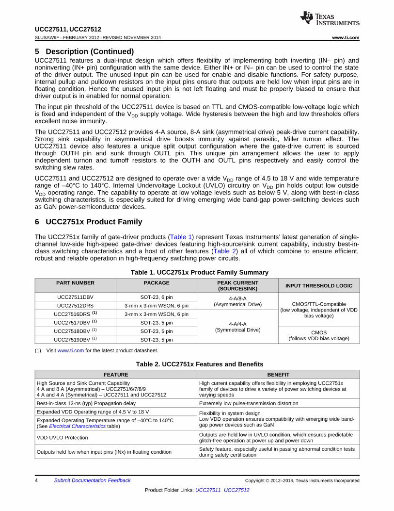
7 Pin Configuration and Functions
6-PinsDBV Package
(Top View)
6-Pins
Copyright © 2012–2014, Texas Instruments Incorporated Submit Documentation Feedback 5
Product Folder Links: UCC27511 UCC27512
UCC27511, UCC27512SLUSAW9F –FEBRUARY 2012–REVISED NOVEMBER 2014 www.ti.com
Pin Functions - UCC27511PIN
I/O DESCRIPTIONNO. NAME
1 VDD I Bias supply input.Sourcing current output of driver. Connect resistor between OUTH and Gate of2 OUTH O power-switching device to adjust turnon speed.Sinking current output of driver. Connect resistor between OUTL and Gate of3 OUTL O power-switching device to adjust turnoff speed.
4 GND - Ground: All signals referenced to this pin.Inverting input: When the driver is used in noninverting configuration, connect IN- to5 IN- I GND in order to enable output, OUT held LOW if IN- is unbiased or floatingNoninverting input: When the driver is used in inverting configuration, connect IN+6 IN+ I to VDD in order to enable output, OUT held LOW if IN+ is unbiased or floating
Pin Functions - UCC27512PIN
I/O DESCRIPTIONNO. NAME
1 IN+ I Noninverting input: When the driver is used in inverting configuration, connect IN+to VDD in order to enable output, OUT held LOW if IN+ is unbiased or floating.
2, 5 GND - Ground: All signals referenced to this pin. TI recommends to connect pin 2 and pin 5on PCB as close to the device as possible.
3 VDD I Bias supply input.4 OUT O Sourcing/sinking current output of driver.6 IN- I Inverting input: When the driver is used in noninverting configuration, connect IN- to
GND in order to enable output, OUT held LOW if IN- is unbiased or floating.
6 Submit Documentation Feedback Copyright © 2012–2014, Texas Instruments Incorporated
Product Folder Links: UCC27511 UCC27512
UCC27511, UCC27512www.ti.com SLUSAW9F –FEBRUARY 2012–REVISED NOVEMBER 2014
8 Specifications
8.1 Absolute Maximum Ratings (1) (2) (3)
over operating free-air temperature range (unless otherwise noted)MIN MAX UNIT
Supply voltage range VDD –0.3 20OUTH voltage, (UCC27511) –0.3 VDD + 0.3
DC –0.3 20OUTL voltage, (UCC27511) V
Repetitive pulse less than 200 ns (4) –2 20DC –0.3 VDD + 0.3
OUT voltage, (UCC27512)Repetitive pulse less than 200 ns (4) –2 VDD + 0.3IOUT_DC (source) 0.3Output continuous current
(OUTH source current and OUTL sink current) IOUT_DC (sink) 0.6A
IOUT_pulsed(source) 4Output pulsed current (0.5 µs)(OUTH source current and OUTL sink current) IOUT_pulsed(sink) 8IN+, IN– (5) –0.3 20 V
Soldering, 10 sec. 300Lead temperature °C
Reflow 260
(1) Stresses beyond those listed under Absolute Maximum Ratings may cause permanent damage to the device. These are stress ratingsonly and functional operation of the device at these or any other conditions beyond those indicated under Recommended OperatingConditions is not implied. Exposure to absolute-maximum-rated conditions for extended periods may affect device reliability.
(2) All voltages are with respect to GND unless otherwise noted. Currents are positive into and negative out of the specified terminal. SeePackaging Section of the datasheet for thermal limitations and considerations of packages.
(3) These devices are sensitive to electrostatic discharge; follow proper device handling procedures.(4) Values are verified by characterization on bench.(5) Maximum voltage on input pins is not restricted by the voltage on the VDD pin.
8.2 Handling RatingsMIN MAX UNIT
Tstg Storage temperature range –65 150 °CHuman body model (HBM), per ANSI/ESDA/JEDEC JS-001, all –4000 4000pins (1)
V(ESD) Electrostatic discharge VCharged device model (CDM), per JEDEC specification –1000 1000JESD22-C101, all pins (2)
(1) JEDEC document JEP155 states that 500-V HBM allows safe manufacturing with a standard ESD control process.(2) JEDEC document JEP157 states that 250-V CDM allows safe manufacturing with a standard ESD control process.
8.3 Recommended Operating Conditionsover operating free-air temperature range (unless otherwise noted)
MIN TYP MAX UNITSupply voltage range, VDD 4.5 12 18 VOperating junction temperature range –40 140 °CInput voltage, IN+ and IN- 0 18 V
Copyright © 2012–2014, Texas Instruments Incorporated Submit Documentation Feedback 7
Product Folder Links: UCC27511 UCC27512
UCC27511, UCC27512SLUSAW9F –FEBRUARY 2012–REVISED NOVEMBER 2014 www.ti.com
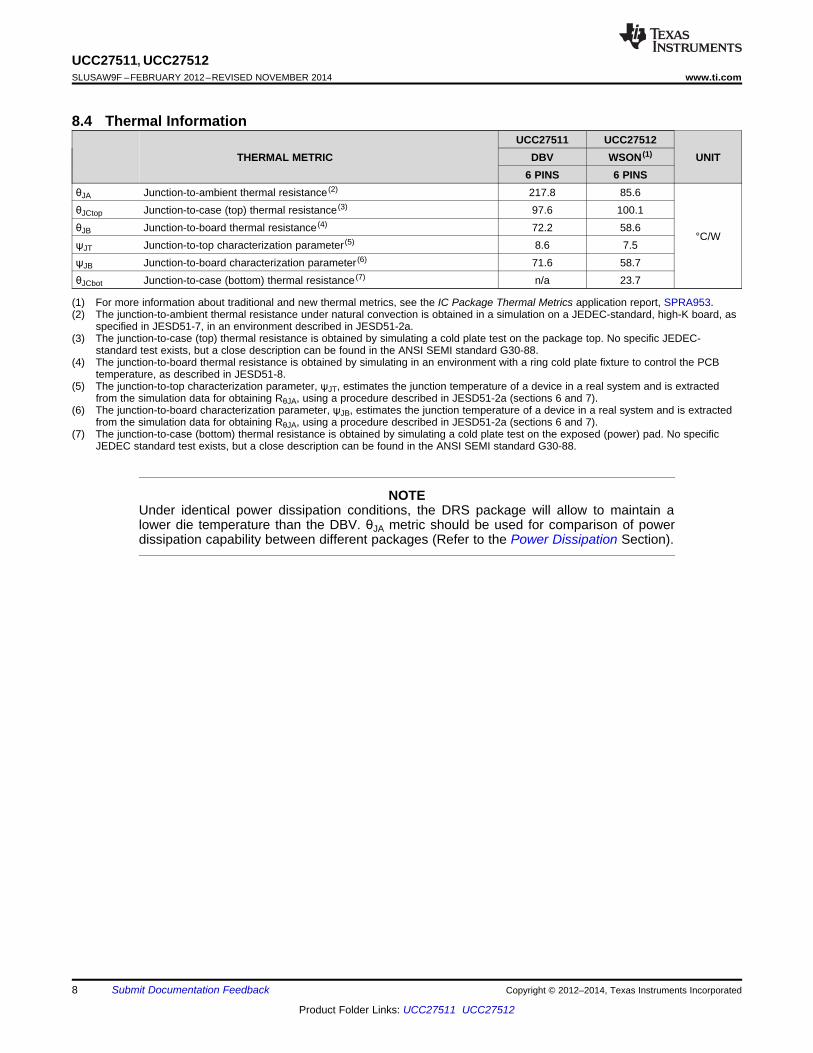
8.4 Thermal InformationUCC27511 UCC27512
THERMAL METRIC DBV WSON (1) UNIT6 PINS 6 PINS
θJA Junction-to-ambient thermal resistance (2) 217.8 85.6θJCtop Junction-to-case (top) thermal resistance (3) 97.6 100.1θJB Junction-to-board thermal resistance (4) 72.2 58.6
°C/WψJT Junction-to-top characterization parameter (5) 8.6 7.5ψJB Junction-to-board characterization parameter (6) 71.6 58.7θJCbot Junction-to-case (bottom) thermal resistance (7) n/a 23.7
(1) For more information about traditional and new thermal metrics, see the IC Package Thermal Metrics application report, SPRA953.(2) The junction-to-ambient thermal resistance under natural convection is obtained in a simulation on a JEDEC-standard, high-K board, as
specified in JESD51-7, in an environment described in JESD51-2a.(3) The junction-to-case (top) thermal resistance is obtained by simulating a cold plate test on the package top. No specific JEDEC-
standard test exists, but a close description can be found in the ANSI SEMI standard G30-88.(4) The junction-to-board thermal resistance is obtained by simulating in an environment with a ring cold plate fixture to control the PCB
temperature, as described in JESD51-8.(5) The junction-to-top characterization parameter, ψJT, estimates the junction temperature of a device in a real system and is extracted
from the simulation data for obtaining RθJA, using a procedure described in JESD51-2a (sections 6 and 7).(6) The junction-to-board characterization parameter, ψJB, estimates the junction temperature of a device in a real system and is extracted
from the simulation data for obtaining RθJA, using a procedure described in JESD51-2a (sections 6 and 7).(7) The junction-to-case (bottom) thermal resistance is obtained by simulating a cold plate test on the exposed (power) pad. No specific
JEDEC standard test exists, but a close description can be found in the ANSI SEMI standard G30-88.Spacer
NOTEUnder identical power dissipation conditions, the DRS package will allow to maintain alower die temperature than the DBV. θJA metric should be used for comparison of powerdissipation capability between different packages (Refer to the Power Dissipation Section).
8 Submit Documentation Feedback Copyright © 2012–2014, Texas Instruments Incorporated
Product Folder Links: UCC27511 UCC27512
UCC27511, UCC27512www.ti.com SLUSAW9F –FEBRUARY 2012–REVISED NOVEMBER 2014
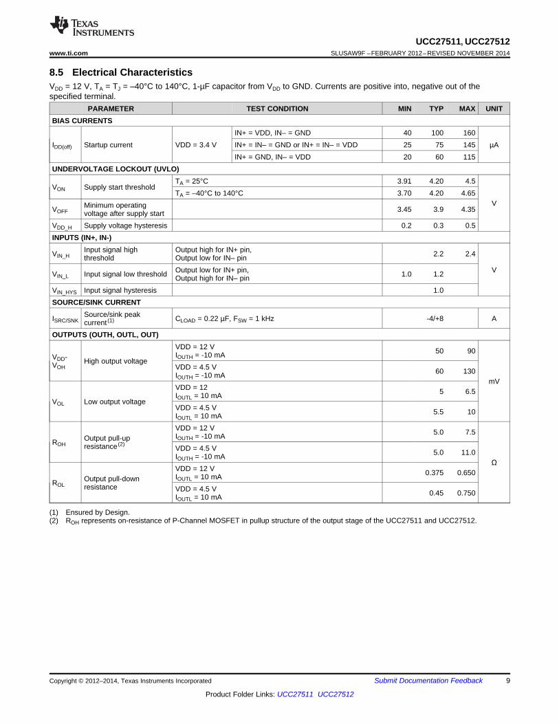
8.5 Electrical CharacteristicsVDD = 12 V, TA = TJ = –40°C to 140°C, 1-µF capacitor from VDD to GND. Currents are positive into, negative out of thespecified terminal.
PARAMETER TEST CONDITION MIN TYP MAX UNITBIAS CURRENTS
IN+ = VDD, IN– = GND 40 100 160IDD(off) Startup current VDD = 3.4 V IN+ = IN– = GND or IN+ = IN– = VDD 25 75 145 µA
IN+ = GND, IN– = VDD 20 60 115UNDERVOLTAGE LOCKOUT (UVLO)
TA = 25°C 3.91 4.20 4.5VON Supply start threshold
TA = –40°C to 140°C 3.70 4.20 4.65VMinimum operatingVOFF 3.45 3.9 4.35voltage after supply start
VDD_H Supply voltage hysteresis 0.2 0.3 0.5INPUTS (IN+, IN-)
Input signal high Output high for IN+ pin,VIN_H 2.2 2.4threshold Output low for IN– pinOutput low for IN+ pin, VVIN_L Input signal low threshold 1.0 1.2Output high for IN– pin
VIN_HYS Input signal hysteresis 1.0SOURCE/SINK CURRENT
Source/sink peakISRC/SNK CLOAD = 0.22 µF, FSW = 1 kHz -4/+8 Acurrent (1)
OUTPUTS (OUTH, OUTL, OUT)VDD = 12 V 50 90IOUTH = -10 mAVDD- High output voltageVOH VDD = 4.5 V 60 130IOUTH = -10 mA
mVVDD = 12 5 6.5IOUTL = 10 mA
VOL Low output voltageVDD = 4.5 V 5.5 10IOUTL = 10 mAVDD = 12 V 5.0 7.5IOUTH = -10 mAOutput pull-upROH resistance (2) VDD = 4.5 V 5.0 11.0IOUTH = -10 mA
ΩVDD = 12 V 0.375 0.650IOUTL = 10 mAOutput pull-downROL resistance VDD = 4.5 V 0.45 0.750IOUTL = 10 mA
(1) Ensured by Design.(2) ROH represents on-resistance of P-Channel MOSFET in pullup structure of the output stage of the UCC27511 and UCC27512.
Copyright © 2012–2014, Texas Instruments Incorporated Submit Documentation Feedback 9
Product Folder Links: UCC27511 UCC27512
tD1 tD1
Low
90%
10%
IN- pin
OUTPUT
High
INPUT
(IN+ pin)
Low
High
tft rtD1 tD1
Low
90%
10%
IN- pin
OUTPUT
High
INPUT
(IN+ pin)
Low
High
tft r
UCC27511, UCC27512SLUSAW9F –FEBRUARY 2012–REVISED NOVEMBER 2014 www.ti.com
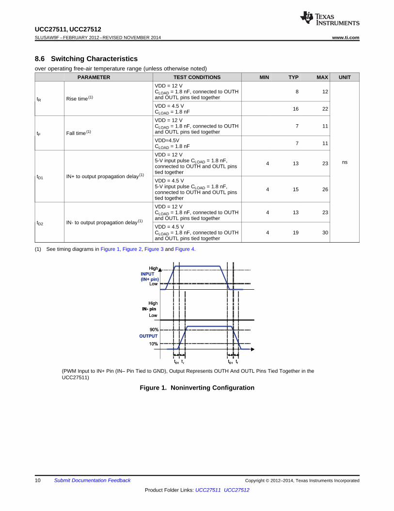
8.6 Switching Characteristicsover operating free-air temperature range (unless otherwise noted)
PARAMETER TEST CONDITIONS MIN TYP MAX UNITVDD = 12 VCLOAD = 1.8 nF, connected to OUTH 8 12and OUTL pins tied togethertR Rise time (1)
VDD = 4.5 V 16 22CLOAD = 1.8 nFVDD = 12 VCLOAD = 1.8 nF, connected to OUTH 7 11and OUTL pins tied togethertF Fall time (1)
VDD=4.5V 7 11CLOAD = 1.8 nFVDD = 12 V5-V input pulse CLOAD = 1.8 nF, ns4 13 23connected to OUTH and OUTL pinstied together
tD1 IN+ to output propagation delay (1)VDD = 4.5 V5-V input pulse CLOAD = 1.8 nF, 4 15 26connected to OUTH and OUTL pinstied togetherVDD = 12 VCLOAD = 1.8 nF, connected to OUTH 4 13 23and OUTL pins tied together
tD2 IN- to output propagation delay (1)VDD = 4.5 VCLOAD = 1.8 nF, connected to OUTH 4 19 30and OUTL pins tied together
(1) See timing diagrams in Figure 1, Figure 2, Figure 3 and Figure 4.
(PWM Input to IN+ Pin (IN– Pin Tied to GND), Output Represents OUTH And OUTL Pins Tied Together in theUCC27511)
Figure 1. Noninverting Configuration
10 Submit Documentation Feedback Copyright © 2012–2014, Texas Instruments Incorporated
Product Folder Links: UCC27511 UCC27512
tD2 tD2
90%
10%
OUTPUT
Low
ENABLE
(IN- pin)
High
Low
High
INPUT
(IN+ pin)
trt ftD2 tD2
90%
10%
OUTPUT
Low
ENABLE
(IN- pin)
High
Low
High
INPUT
(IN+ pin)
trt f
Low
90%
10%
ENABLE
(IN+ pin)
OUTPUT
tD1
High
tD1
Low
High
INPUT
(IN- pin)
tr
tf
Low
90%
10%
ENABLE
(IN+ pin)
OUTPUT
tD1
High
tD1
Low
High
INPUT
(IN- pin)
tr
tf
tD2
tD2
90%
10%
OUTPUT
Low
High
IN+ pin
Low
High
INPUT
(IN- pin)
tf
tr
tD2
tD2
90%
10%
OUTPUT
Low
High
IN+ pin
Low
High
INPUT
(IN- pin)
tf
tr
UCC27511, UCC27512www.ti.com SLUSAW9F –FEBRUARY 2012–REVISED NOVEMBER 2014
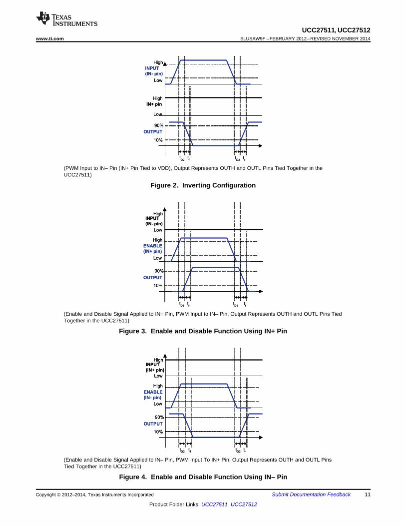
(PWM Input to IN– Pin (IN+ Pin Tied to VDD), Output Represents OUTH and OUTL Pins Tied Together in theUCC27511)
Figure 2. Inverting Configuration
(Enable and Disable Signal Applied to IN+ Pin, PWM Input to IN– Pin, Output Represents OUTH and OUTL Pins TiedTogether in the UCC27511)
Figure 3. Enable and Disable Function Using IN+ Pin
(Enable and Disable Signal Applied to IN– Pin, PWM Input To IN+ Pin, Output Represents OUTH and OUTL PinsTied Together in the UCC27511)
Figure 4. Enable and Disable Function Using IN– Pin
Copyright © 2012–2014, Texas Instruments Incorporated Submit Documentation Feedback 11
Product Folder Links: UCC27511 UCC27512
1
1.5
2
2.5
3
3.5
−50 0 50 100 150Temperature (°C)
Inpu
t Thr
esho
ld (
V)
Turn−OnTurn−Off
VDD = 12 VCLoad = 1.8 nF
G014
4
5
6
7
8
−50 0 50 100 150Temperature (°C)
Out
put P
ull−
Up
Res
ista
nce
(Ω)
RoH
VDD = 12 VIout = 10 mA
G004
0.1
0.2
0.3
0.4
0.5
−50 0 50 100 150Temperature (°C)
Ope
ratin
g S
uppl
y C
urre
nt (
mA
)
IN+=Low,IN−=LowIN+=High, IN−=Low
VDD = 12 V
G002
3.6
3.8
4
4.2
4.4
4.6
−50 0 50 100 150Temperature (°C)
UV
LO T
hres
hold
(V
)
UVLO RisingUVLO Falling
G003
0.05
0.06
0.07
0.08
0.09
0.1
0.11
0.12
−50 0 50 100 150Temperature (°C)
Sta
rtup
Cur
rent
(m
A)
IN+=Low,IN−=LowIN+=High, IN−=Low
VDD = 3.4 V
G001
2
2.5
3
3.5
4
−50 0 50 100 150Temperature (°C)
IDD
(m
A)
VDD = 12 VCLoad = 500 pFfsw = 500 kHz
G013
UCC27511, UCC27512SLUSAW9F –FEBRUARY 2012–REVISED NOVEMBER 2014 www.ti.com
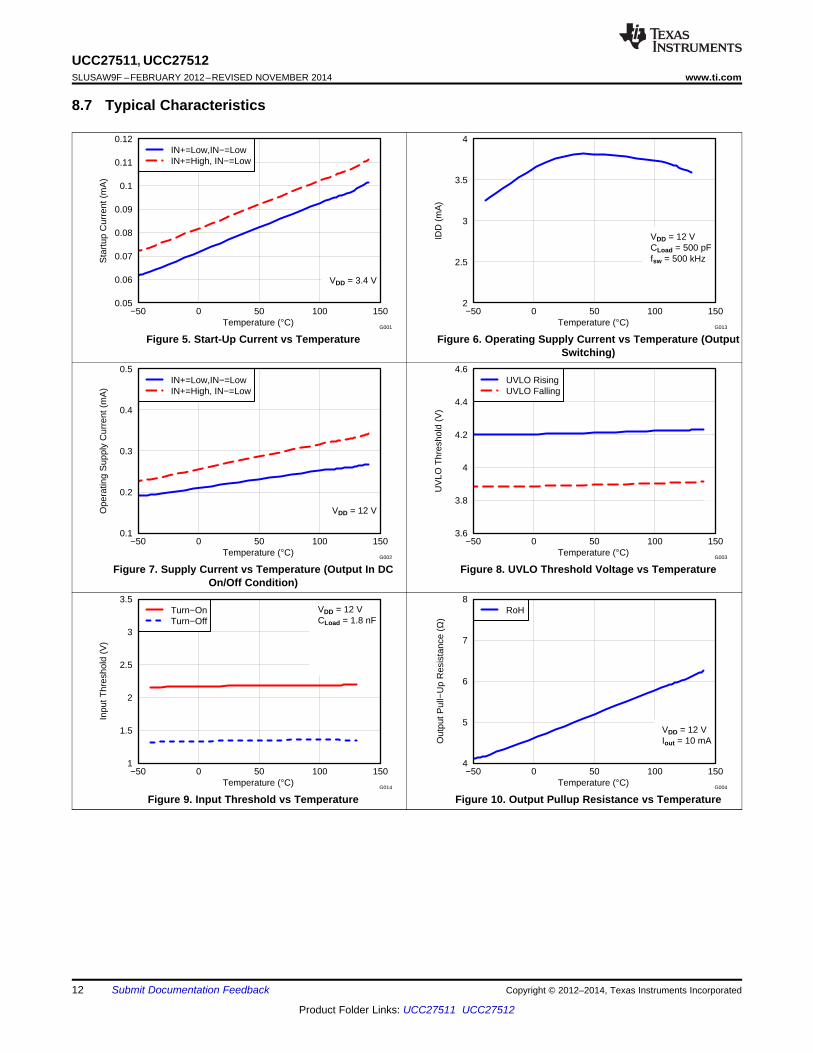
8.7 Typical Characteristics
Figure 5. Start-Up Current vs Temperature Figure 6. Operating Supply Current vs Temperature (OutputSwitching)
Figure 7. Supply Current vs Temperature (Output In DC Figure 8. UVLO Threshold Voltage vs TemperatureOn/Off Condition)
Figure 9. Input Threshold vs Temperature Figure 10. Output Pullup Resistance vs Temperature
12 Submit Documentation Feedback Copyright © 2012–2014, Texas Instruments Incorporated
Product Folder Links: UCC27511 UCC27512
0
2
4
6
8
10
12
14
16
18
20
0 100 200 300 400 500 600 700Frequency (kHz)
Sup
ply
Cur
rent
(m
A)
VDD=4.5VVDD=12VVDD=15V
CLoad = 1.8 nF
G010
6
8
10
12
14
16
18
20
0 4 8 12 16 20Supply Voltage (V)
Pro
paga
tion
Del
ay (
ns)
Turn−OnTurn−Off
G007
6
7
8
9
10
−50 0 50 100 150Temperature (°C)
Fal
l Tim
e (n
s)
VDD = 12 VCLoad = 1.8 nF
G000
5
10
15
20
−50 0 50 100 150Temperature (°C)
Pro
paga
tion
Del
ay (
ns)
Turn−OnTurn−Off
VDD = 12 V
G006
0.1
0.3
0.5
0.7
0.8
−50 0 50 100 150Temperature (°C)
Out
put P
ull−
Dow
n R
esis
tanc
e (Ω
) ROL
VDD = 12 VIout = 10 mA
G005
4
5
6
7
8
−50 0 50 100 150Temperature (°C)
Ris
e T
ime
(ns)
VDD = 12 VCLoad = 1.8 nF
G000
UCC27511, UCC27512www.ti.com SLUSAW9F –FEBRUARY 2012–REVISED NOVEMBER 2014
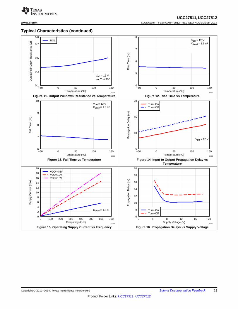
Typical Characteristics (continued)
Figure 11. Output Pulldown Resistance vs Temperature Figure 12. Rise Time vs Temperature
Figure 13. Fall Time vs Temperature Figure 14. Input to Output Propagation Delay vsTemperature
Figure 15. Operating Supply Current vs Frequency Figure 16. Propagation Delays vs Supply Voltage
Copyright © 2012–2014, Texas Instruments Incorporated Submit Documentation Feedback 13
Product Folder Links: UCC27511 UCC27512
5
10
15
20
0 4 8 12 16 20Supply Voltage (V)
Ris
e T
ime
(ns)
G008
2
4
6
8
10
0 4 8 12 16 20Supply Voltage (V)
Fal
l Tim
e (n
s)
G009
UCC27511, UCC27512SLUSAW9F –FEBRUARY 2012–REVISED NOVEMBER 2014 www.ti.com
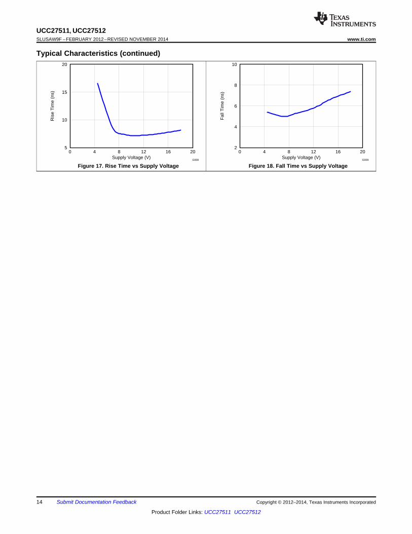
Typical Characteristics (continued)
Figure 17. Rise Time vs Supply Voltage Figure 18. Fall Time vs Supply Voltage
14 Submit Documentation Feedback Copyright © 2012–2014, Texas Instruments Incorporated
Product Folder Links: UCC27511 UCC27512
6
5
4
1
2
3
200 kW
VDD230 kW
UVLO
VDD
VDD
VDD
OUTH
OUTL
IN+
IN-
GND
UCC27511, UCC27512www.ti.com SLUSAW9F –FEBRUARY 2012–REVISED NOVEMBER 2014
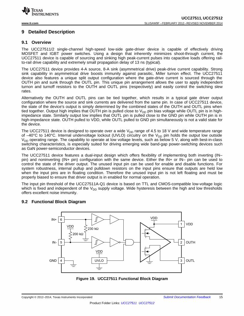
9 Detailed Description
9.1 OverviewThe UCC27511/2 single-channel high-speed low-side gate-driver device is capable of effectively drivingMOSFET and IGBT power switches. Using a design that inherently minimizes shoot-through current, theUCC27511 device is capable of sourcing and sinking high peak-current pulses into capacitive loads offering rail-to-rail drive capability and extremely small propagation delay of 13 ns (typical).
The UCC27511 device provides 4-A source, 8-A sink (asymmetrical drive) peak-drive current capability. Strongsink capability in asymmetrical drive boosts immunity against parasitic, Miller turnon effect. The UCC27511device also features a unique split output configuration where the gate-drive current is sourced through theOUTH pin and sunk through the OUTL pin. This unique pin arrangement allows the user to apply independentturnon and turnoff resistors to the OUTH and OUTL pins (respectively) and easily control the switching slewrates.
Alternatively the OUTH and OUTL pins can be tied together, which results in a typical gate driver outputconfiguration where the source and sink currents are delivered from the same pin. In case of UCC27511 device,the state of the device's output is simply determined by the combined states of the OUTH and OUTL pins whentied together. Output high implies that OUTH pin is pulled close to VDD pin bias voltage while OUTL pin is in high-impedance state. Similarly output low implies that OUTL pin is pulled close to the GND pin while OUTH pin is inhigh-impedance state. OUTH pulled to VDD, while OUTL pulled to GND pin simultaneously is not a valid state forthe device.
The UCC27511 device is designed to operate over a wide VDD range of 4.5 to 18 V and wide temperature rangeof –40°C to 140°C. Internal undervoltage lockout (UVLO) circuitry on the VDD pin holds the output low outsideVDD operating range. The capability to operate at low voltage levels, such as below 5 V, along with best-in-classswitching characteristics, is especially suited for driving emerging wide band-gap power-switching devices suchas GaN power-semiconductor devices.
The UCC27511 device features a dual-input design which offers flexibility of implementing both inverting (IN–pin) and noninverting (IN+ pin) configuration with the same device. Either the IN+ or IN– pin can be used tocontrol the state of the driver output. The unused input pin can be used for enable and disable functions. Forsystem robustness, internal pullup and pulldown resistors on the input pins ensure that outputs are held lowwhen the input pins are in floating condition. Therefore the unused input pin is not left floating and must beproperly biased to ensure that driver output is in enabled for normal operation.
The input pin threshold of the UCC27511A-Q1 device is based on TTL and CMOS-compatible low-voltage logicwhich is fixed and independent of the VDD supply voltage. Wide hysteresis between the high and low thresholdsoffers excellent noise immunity.
9.2 Functional Block Diagram
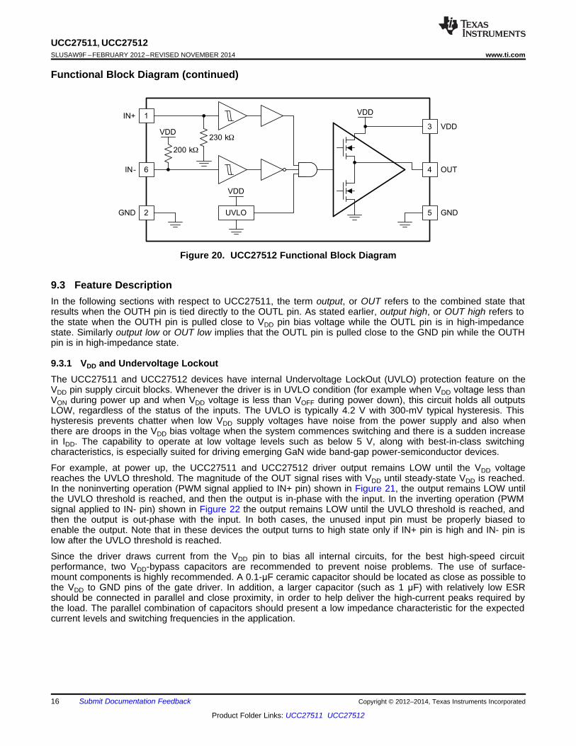
Figure 19. UCC27511 Functional Block Diagram
Copyright © 2012–2014, Texas Instruments Incorporated Submit Documentation Feedback 15
Product Folder Links: UCC27511 UCC27512
1
6
2
3
4
5
200 kW
VDD230 kW
UVLO
VDD
VDD
VDD
OUT
GND
IN+
IN-
GND
UCC27511, UCC27512SLUSAW9F –FEBRUARY 2012–REVISED NOVEMBER 2014 www.ti.com
Functional Block Diagram (continued)
Figure 20. UCC27512 Functional Block Diagram
9.3 Feature DescriptionIn the following sections with respect to UCC27511, the term output, or OUT refers to the combined state thatresults when the OUTH pin is tied directly to the OUTL pin. As stated earlier, output high, or OUT high refers tothe state when the OUTH pin is pulled close to VDD pin bias voltage while the OUTL pin is in high-impedancestate. Similarly output low or OUT low implies that the OUTL pin is pulled close to the GND pin while the OUTHpin is in high-impedance state.
9.3.1 VDD and Undervoltage LockoutThe UCC27511 and UCC27512 devices have internal Undervoltage LockOut (UVLO) protection feature on theVDD pin supply circuit blocks. Whenever the driver is in UVLO condition (for example when VDD voltage less thanVON during power up and when VDD voltage is less than VOFF during power down), this circuit holds all outputsLOW, regardless of the status of the inputs. The UVLO is typically 4.2 V with 300-mV typical hysteresis. Thishysteresis prevents chatter when low VDD supply voltages have noise from the power supply and also whenthere are droops in the VDD bias voltage when the system commences switching and there is a sudden increasein IDD. The capability to operate at low voltage levels such as below 5 V, along with best-in-class switchingcharacteristics, is especially suited for driving emerging GaN wide band-gap power-semiconductor devices.
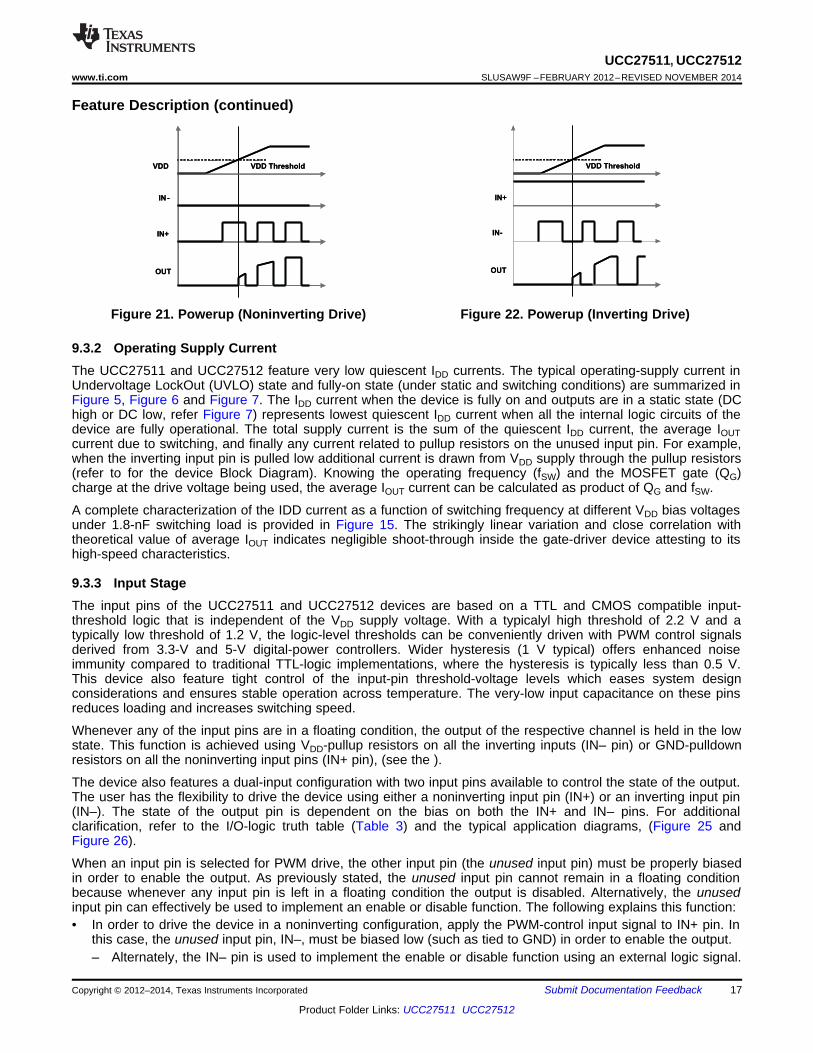
For example, at power up, the UCC27511 and UCC27512 driver output remains LOW until the VDD voltagereaches the UVLO threshold. The magnitude of the OUT signal rises with VDD until steady-state VDD is reached.In the noninverting operation (PWM signal applied to IN+ pin) shown in Figure 21, the output remains LOW untilthe UVLO threshold is reached, and then the output is in-phase with the input. In the inverting operation (PWMsignal applied to IN- pin) shown in Figure 22 the output remains LOW until the UVLO threshold is reached, andthen the output is out-phase with the input. In both cases, the unused input pin must be properly biased toenable the output. Note that in these devices the output turns to high state only if IN+ pin is high and IN- pin islow after the UVLO threshold is reached.
Since the driver draws current from the VDD pin to bias all internal circuits, for the best high-speed circuitperformance, two VDD-bypass capacitors are recommended to prevent noise problems. The use of surface-mount components is highly recommended. A 0.1-μF ceramic capacitor should be located as close as possible tothe VDD to GND pins of the gate driver. In addition, a larger capacitor (such as 1 μF) with relatively low ESRshould be connected in parallel and close proximity, in order to help deliver the high-current peaks required bythe load. The parallel combination of capacitors should present a low impedance characteristic for the expectedcurrent levels and switching frequencies in the application.
16 Submit Documentation Feedback Copyright © 2012–2014, Texas Instruments Incorporated
Product Folder Links: UCC27511 UCC27512
VDD ThresholdVDD
IN+
OUT
IN-
VDD ThresholdVDD
IN+
OUT
IN-
VDD Threshold
IN-
OUT
IN+
VDD Threshold
IN-
OUT
IN+
UCC27511, UCC27512www.ti.com SLUSAW9F –FEBRUARY 2012–REVISED NOVEMBER 2014
Feature Description (continued)
Figure 21. Powerup (Noninverting Drive) Figure 22. Powerup (Inverting Drive)
9.3.2 Operating Supply CurrentThe UCC27511 and UCC27512 feature very low quiescent IDD currents. The typical operating-supply current inUndervoltage LockOut (UVLO) state and fully-on state (under static and switching conditions) are summarized inFigure 5, Figure 6 and Figure 7. The IDD current when the device is fully on and outputs are in a static state (DChigh or DC low, refer Figure 7) represents lowest quiescent IDD current when all the internal logic circuits of thedevice are fully operational. The total supply current is the sum of the quiescent IDD current, the average IOUTcurrent due to switching, and finally any current related to pullup resistors on the unused input pin. For example,when the inverting input pin is pulled low additional current is drawn from VDD supply through the pullup resistors(refer to for the device Block Diagram). Knowing the operating frequency (fSW) and the MOSFET gate (QG)charge at the drive voltage being used, the average IOUT current can be calculated as product of QG and fSW.
A complete characterization of the IDD current as a function of switching frequency at different VDD bias voltagesunder 1.8-nF switching load is provided in Figure 15. The strikingly linear variation and close correlation withtheoretical value of average IOUT indicates negligible shoot-through inside the gate-driver device attesting to itshigh-speed characteristics.
9.3.3 Input StageThe input pins of the UCC27511 and UCC27512 devices are based on a TTL and CMOS compatible input-threshold logic that is independent of the VDD supply voltage. With a typicalyl high threshold of 2.2 V and atypically low threshold of 1.2 V, the logic-level thresholds can be conveniently driven with PWM control signalsderived from 3.3-V and 5-V digital-power controllers. Wider hysteresis (1 V typical) offers enhanced noiseimmunity compared to traditional TTL-logic implementations, where the hysteresis is typically less than 0.5 V.This device also feature tight control of the input-pin threshold-voltage levels which eases system designconsiderations and ensures stable operation across temperature. The very-low input capacitance on these pinsreduces loading and increases switching speed.
Whenever any of the input pins are in a floating condition, the output of the respective channel is held in the lowstate. This function is achieved using VDD-pullup resistors on all the inverting inputs (IN– pin) or GND-pulldownresistors on all the noninverting input pins (IN+ pin), (see the ).
The device also features a dual-input configuration with two input pins available to control the state of the output.The user has the flexibility to drive the device using either a noninverting input pin (IN+) or an inverting input pin(IN–). The state of the output pin is dependent on the bias on both the IN+ and IN– pins. For additionalclarification, refer to the I/O-logic truth table (Table 3) and the typical application diagrams, (Figure 25 andFigure 26).
When an input pin is selected for PWM drive, the other input pin (the unused input pin) must be properly biasedin order to enable the output. As previously stated, the unused input pin cannot remain in a floating conditionbecause whenever any input pin is left in a floating condition the output is disabled. Alternatively, the unusedinput pin can effectively be used to implement an enable or disable function. The following explains this function:• In order to drive the device in a noninverting configuration, apply the PWM-control input signal to IN+ pin. In
this case, the unused input pin, IN–, must be biased low (such as tied to GND) in order to enable the output.– Alternately, the IN– pin is used to implement the enable or disable function using an external logic signal.
Copyright © 2012–2014, Texas Instruments Incorporated Submit Documentation Feedback 17
Product Folder Links: UCC27511 UCC27512
UCC27511, UCC27512SLUSAW9F –FEBRUARY 2012–REVISED NOVEMBER 2014 www.ti.com
Feature Description (continued)OUT is disabled when IN– is biased high and OUT is enabled when IN– is biased low.
• In order to drive the device in an inverting configuration, apply the PWM-control input signal to IN– pin. In thiscase, the unused input pin, IN+, must be biased high (such as tied to VDD) in order to enable the output.– Alternately, the IN+ pin is used to implement the enable or disable function using an external logic signal.
OUT is disabled when IN+ is biased low and OUT is enabled when IN+ is biased high.• Finally, note that the output pin can be driven into a high state only when the IN+ pin is biased high and the
IN– input is biased low.
The input stage of the driver is preferably driven by a signal with a short rise or fall time. Use caution wheneverthe driver is used with slowly varying input signals, especially in situations where the device is located in amechanical socket or PCB layout that is not optimal:• High dI/dt current from the driver output coupled with board layout parasitics can cause ground bounce. The
differential voltage between input pins and GND is modified and triggers an unintended change of outputstate because of fast 13-ns propagation delay which can ultimately result in high-frequency oscillations thatincrease power dissipation and pose a risk of damage to the device.
• A 1-V input-threshold hysteresis boosts noise immunity compared to most other industry standard drivers.• In the worst case, when a slow input signal is used and PCB layout is not optimal, adding a small capacitor (1
nF) between the input pin and GND pin very close to the driver device may be necessary which helps toconvert the differential mode noise with respect to the input-logic circuitry into common-mode noise and avoidunintended change of output state.
If limiting the rise or fall times to the power device is the primary goal, then an external resistance is highlyrecommended between the output of the driver and the power device instead of adding delays on the inputsignal. This external resistor has the additional benefit of reducing part of the gate-charge related powerdissipation in the gate-driver device package and transferring the power dissipation into the external resistor.
9.3.4 Enable FunctionAs mentioned earlier, an enable and disable function is easily implemented in UCC27511 and UCC27512devices using the unused input pin. When the IN+ pin is pulled down to GND or the IN– pin is pulled down toVDD, the output is disabled. Thus the IN+ pin can be used like an enable pin that is based on active-high logic,while the IN– pin can be used like an enable pin that is based on active-low logic.
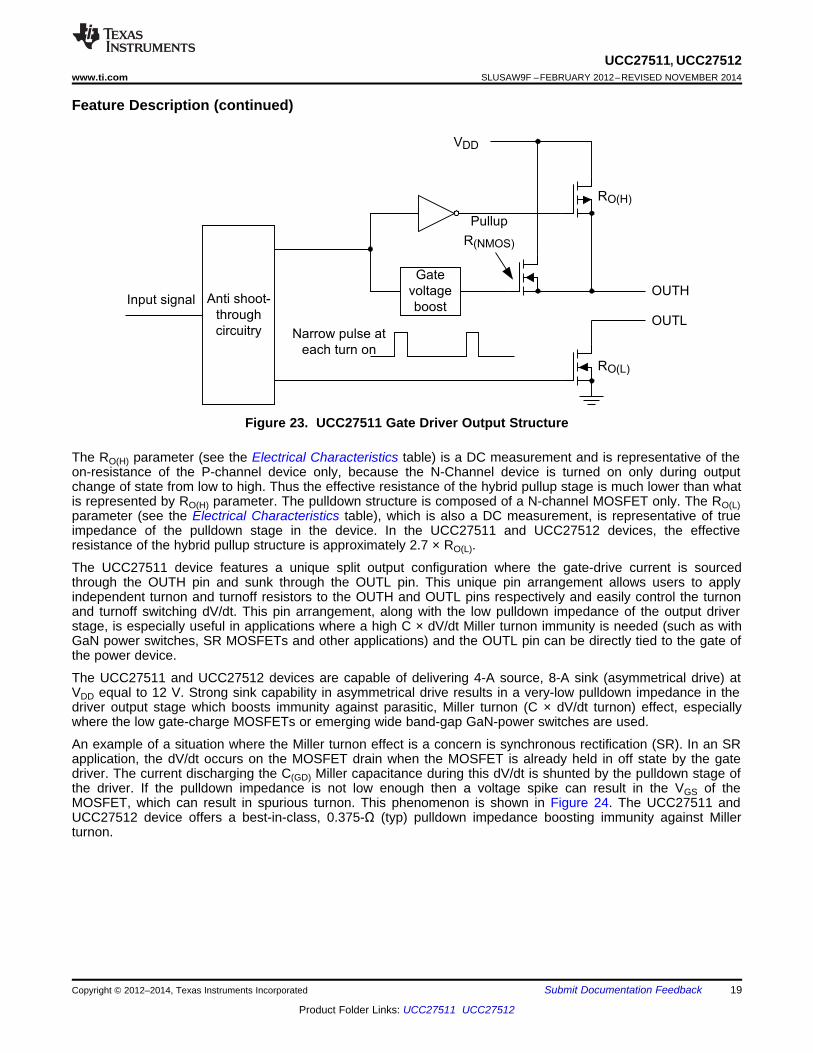
9.3.5 Output StageFigure 23 shows the output stage of the UCC27511 and UCC27512 devices. The UCC27511 and UCC27512devices feature a unique architecture on the output stage which delivers the highest peak-source current whenthe peak source current is most needed during the Miller plateau region of the power switch turnon transition(when the power-switch drain or collector voltage experiences dV/dt). The device output stage features a hybridpullup structure using a parallel arrangement of N-channel and P-channel MOSFET devices. By turning on the N-channel MOSFET during a narrow instant when the output changes state from low to high, the gate-driver deviceis able to deliver a brief boost in the peak-sourcing current enabling fast turnon.
18 Submit Documentation Feedback Copyright © 2012–2014, Texas Instruments Incorporated
Product Folder Links: UCC27511 UCC27512
VDD
RO(H)
RO(L)
Gate
voltage
boost
Narrow pulse at
each turn on
Anti shoot-
through
circuitry
Input signal
Pullup
R(NMOS)
OUTL
OUTH
UCC27511, UCC27512www.ti.com SLUSAW9F –FEBRUARY 2012–REVISED NOVEMBER 2014
Feature Description (continued)
Figure 23. UCC27511 Gate Driver Output Structure
The RO(H) parameter (see the Electrical Characteristics table) is a DC measurement and is representative of theon-resistance of the P-channel device only, because the N-Channel device is turned on only during outputchange of state from low to high. Thus the effective resistance of the hybrid pullup stage is much lower than whatis represented by RO(H) parameter. The pulldown structure is composed of a N-channel MOSFET only. The RO(L)parameter (see the Electrical Characteristics table), which is also a DC measurement, is representative of trueimpedance of the pulldown stage in the device. In the UCC27511 and UCC27512 devices, the effectiveresistance of the hybrid pullup structure is approximately 2.7 × RO(L).
The UCC27511 device features a unique split output configuration where the gate-drive current is sourcedthrough the OUTH pin and sunk through the OUTL pin. This unique pin arrangement allows users to applyindependent turnon and turnoff resistors to the OUTH and OUTL pins respectively and easily control the turnonand turnoff switching dV/dt. This pin arrangement, along with the low pulldown impedance of the output driverstage, is especially useful in applications where a high C × dV/dt Miller turnon immunity is needed (such as withGaN power switches, SR MOSFETs and other applications) and the OUTL pin can be directly tied to the gate ofthe power device.
The UCC27511 and UCC27512 devices are capable of delivering 4-A source, 8-A sink (asymmetrical drive) atVDD equal to 12 V. Strong sink capability in asymmetrical drive results in a very-low pulldown impedance in thedriver output stage which boosts immunity against parasitic, Miller turnon (C × dV/dt turnon) effect, especiallywhere the low gate-charge MOSFETs or emerging wide band-gap GaN-power switches are used.
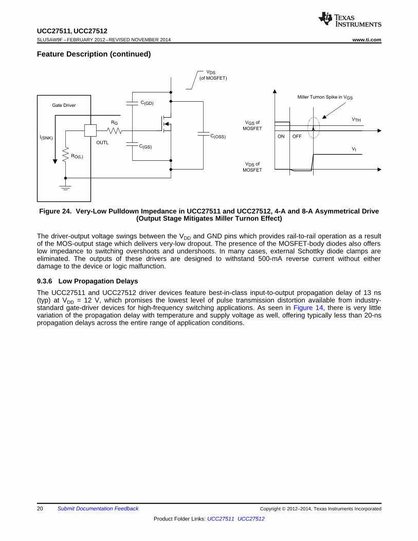
An example of a situation where the Miller turnon effect is a concern is synchronous rectification (SR). In an SRapplication, the dV/dt occurs on the MOSFET drain when the MOSFET is already held in off state by the gatedriver. The current discharging the C(GD) Miller capacitance during this dV/dt is shunted by the pulldown stage ofthe driver. If the pulldown impedance is not low enough then a voltage spike can result in the VGS of theMOSFET, which can result in spurious turnon. This phenomenon is shown in Figure 24. The UCC27511 andUCC27512 device offers a best-in-class, 0.375-Ω (typ) pulldown impedance boosting immunity against Millerturnon.
Copyright © 2012–2014, Texas Instruments Incorporated Submit Documentation Feedback 19
Product Folder Links: UCC27511 UCC27512
Gate Driver
RO(L)
RG
C(GD)
C(GS)
C(OSS)
VDS
I(SNK)
VI
VTH
ON OFF
Miller Turnon Spike in VGS
VDS of
MOSFET
VGS of
MOSFET
OUTL
(of MOSFET)
UCC27511, UCC27512SLUSAW9F –FEBRUARY 2012–REVISED NOVEMBER 2014 www.ti.com
Feature Description (continued)
Figure 24. Very-Low Pulldown Impedance in UCC27511 and UCC27512, 4-A and 8-A Asymmetrical Drive(Output Stage Mitigates Miller Turnon Effect)
The driver-output voltage swings between the VDD and GND pins which provides rail-to-rail operation as a resultof the MOS-output stage which delivers very-low dropout. The presence of the MOSFET-body diodes also offerslow impedance to switching overshoots and undershoots. In many cases, external Schottky diode clamps areeliminated. The outputs of these drivers are designed to withstand 500-mA reverse current without eitherdamage to the device or logic malfunction.
9.3.6 Low Propagation DelaysThe UCC27511 and UCC27512 driver devices feature best-in-class input-to-output propagation delay of 13 ns(typ) at VDD = 12 V, which promises the lowest level of pulse transmission distortion available from industry-standard gate-driver devices for high-frequency switching applications. As seen in Figure 14, there is very littlevariation of the propagation delay with temperature and supply voltage as well, offering typically less than 20-nspropagation delays across the entire range of application conditions.
20 Submit Documentation Feedback Copyright © 2012–2014, Texas Instruments Incorporated
Product Folder Links: UCC27511 UCC27512
UCC27511, UCC27512www.ti.com SLUSAW9F –FEBRUARY 2012–REVISED NOVEMBER 2014
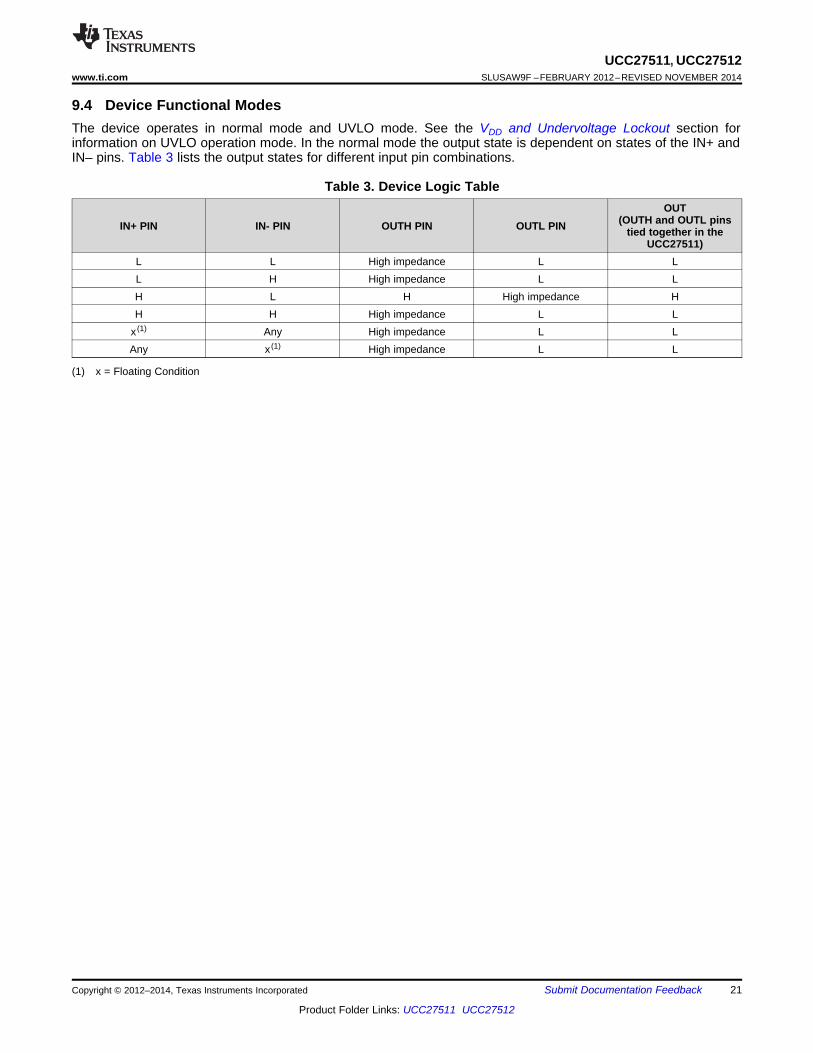
9.4 Device Functional ModesThe device operates in normal mode and UVLO mode. See the VDD and Undervoltage Lockout section forinformation on UVLO operation mode. In the normal mode the output state is dependent on states of the IN+ andIN– pins. Table 3 lists the output states for different input pin combinations.
Table 3. Device Logic TableOUT
(OUTH and OUTL pinsIN+ PIN IN- PIN OUTH PIN OUTL PIN tied together in theUCC27511)
L L High impedance L LL H High impedance L LH L H High impedance HH H High impedance L L
x (1) Any High impedance L LAny x (1) High impedance L L
(1) x = Floating Condition
Copyright © 2012–2014, Texas Instruments Incorporated Submit Documentation Feedback 21
Product Folder Links: UCC27511 UCC27512
6
5
4
1
2
3
IN+
IN-
GND
VDD
OUTH
OUTL
UCC27511
R1
R2
Q1
IN+
D1
C1
+
VOUT
VSOURCE
L1
C2
V+
4.5 V to 18 V
1
2
3
6
5
4
IN+
GND
VDD
IN-
GND
OUT
UCC27512
R3
Q1
IN+
D1
C1
+
VOUT
VSOURCE
L1
C2
V+
4.5 V to 18 V
UCC27511, UCC27512SLUSAW9F –FEBRUARY 2012–REVISED NOVEMBER 2014 www.ti.com
10 Application and Implementation
NOTEInformation in the following applications sections is not part of the TI componentspecification, and TI does not warrant its accuracy or completeness. TI’s customers areresponsible for determining suitability of components for their purposes. Customers shouldvalidate and test their design implementation to confirm system functionality.
10.1 Application InformationHigh-current gate-driver devices are required in switching-power applications for a variety of reasons. In order toeffect fast switching of power devices and reduce associated switching power losses, a powerful gate driveremploys between the PWM output of controllers and the gates of the power-semiconductor devices. Further,gate drivers are indispensable when having the PWM controller directly drive the gates of the switching devicesis impossible. With advent of digital power, this situation will be often encountered since the PWM signal from thedigital controller is often a 3.3-V logic signal which is not capable of effectively turning on a power switch. A level-shifting circuitry is needed to boost the 3.3-V signal to the gate-drive voltage (such as 12 V) in order to fully turnon the power device and minimize conduction losses. Traditional buffer drive circuits based on NPN/PNP bipolartransistors in totem-pole arrangement, being emitter follower configurations, prove inadequate with digital powersince they lack level-shifting capability. Gate drivers effectively combine both the level-shifting and buffer-drivefunctions. Gate drivers also find other needs such as minimizing the effect of high-frequency switching noise bylocating the high-current driver physically close to the power switch, driving gate-drive transformers andcontrolling floating power-device gates, reducing power dissipation and thermal stress in controllers by movinggate charge power losses into itself. Finally, emerging wide band-gap power device technologies such as GaNbased switches, which are capable of supporting very high switching frequency operation, are driving veryspecial requirements in terms of gate drive capability. These requirements include operation at low VDD voltages(5 V or lower), low propagation delays and availability in compact, low-inductance packages with good thermalcapability. In summary gate-driver devices are extremely important components in switching power combiningbenefits of high-performance low-cost component count and board-space reduction and simplified system design.
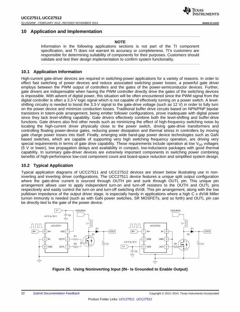
10.2 Typical ApplicationTypical application diagrams of UCC27511 and UCC27512 devices are shown below illustrating use in non-inverting and inverting driver configurations. The UCC27511 device features a unique split output configurationwhere the gate-drive current is sourced through OUTH pin and sunk through OUTL pin. This unique pinarrangement allows user to apply independent turn-on and turn-off resistors to the OUTH and OUTL pinsrespectively and easily control the turn-on and turn-off switching dV/dt. This pin arrangement, along with the lowpulldown impedance of the output driver stage, is especially handy in applications where a high C x dV/dt Millerturnon immunity is needed (such as with GaN power switches, SR MOSFETs, and so forth) and OUTL pin canbe directly tied to the gate of the power device.
Figure 25. Using Noninverting Input (IN– Is Grounded to Enable Output)
22 Submit Documentation Feedback Copyright © 2012–2014, Texas Instruments Incorporated
Product Folder Links: UCC27511 UCC27512
6
5
4
1
2
3
IN+
IN-
GND
VDD
OUTH
OUTL
UCC27511
R1
R2
Q1
IN-
D1
C1
+
VOUT
VSOURCE
L1
C2
V+
4.5 V to 18 V
1
2
3
6
5
4
IN+
GND
VDD
IN-
GND
OUT
UCC27512
R3
Q1
V+
D1
C1
+
VSOURCE
L1
C2
IN-
4.5 V to 18 V
UCC27511, UCC27512www.ti.com SLUSAW9F –FEBRUARY 2012–REVISED NOVEMBER 2014
Typical Application (continued)
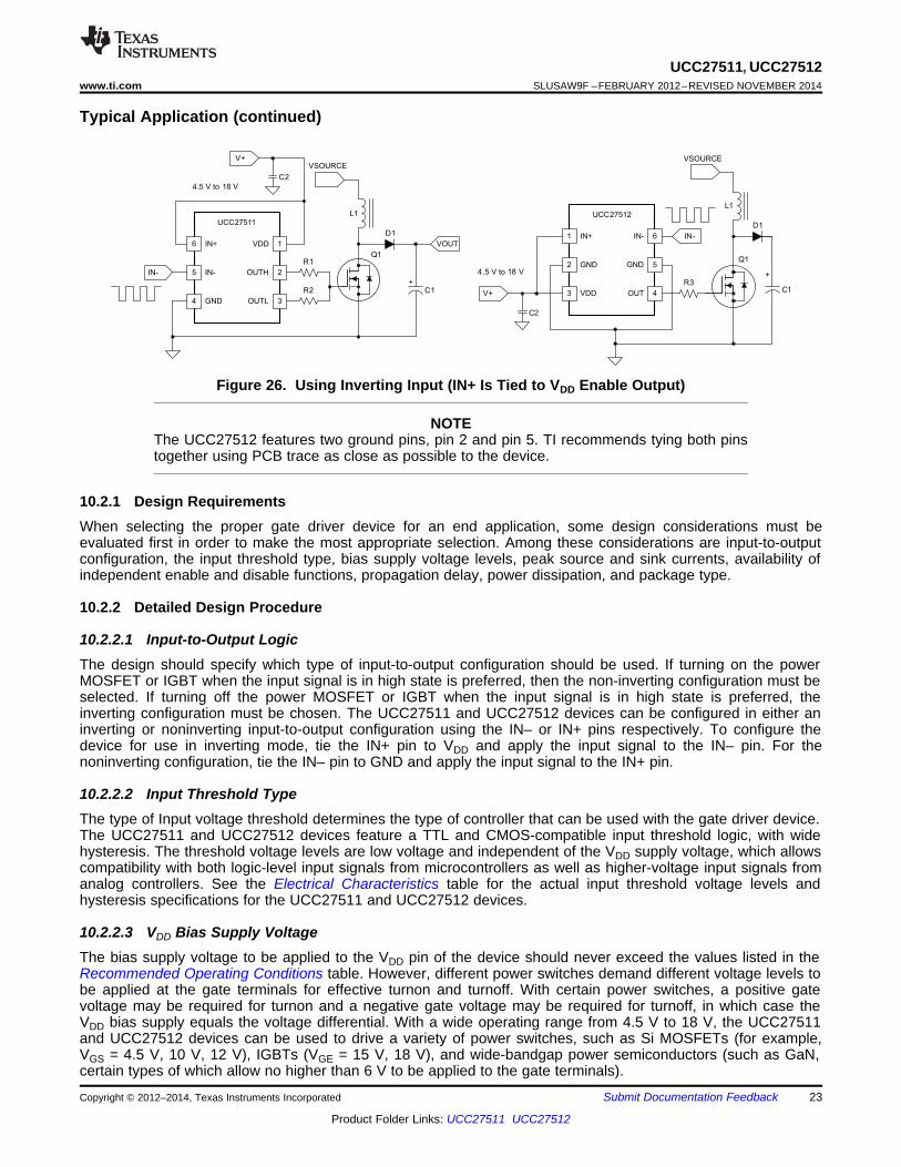
Figure 26. Using Inverting Input (IN+ Is Tied to VDD Enable Output)
NOTEThe UCC27512 features two ground pins, pin 2 and pin 5. TI recommends tying both pinstogether using PCB trace as close as possible to the device.
10.2.1 Design RequirementsWhen selecting the proper gate driver device for an end application, some design considerations must beevaluated first in order to make the most appropriate selection. Among these considerations are input-to-outputconfiguration, the input threshold type, bias supply voltage levels, peak source and sink currents, availability ofindependent enable and disable functions, propagation delay, power dissipation, and package type.
10.2.2 Detailed Design Procedure
10.2.2.1 Input-to-Output LogicThe design should specify which type of input-to-output configuration should be used. If turning on the powerMOSFET or IGBT when the input signal is in high state is preferred, then the non-inverting configuration must beselected. If turning off the power MOSFET or IGBT when the input signal is in high state is preferred, theinverting configuration must be chosen. The UCC27511 and UCC27512 devices can be configured in either aninverting or noninverting input-to-output configuration using the IN– or IN+ pins respectively. To configure thedevice for use in inverting mode, tie the IN+ pin to VDD and apply the input signal to the IN– pin. For thenoninverting configuration, tie the IN– pin to GND and apply the input signal to the IN+ pin.
10.2.2.2 Input Threshold TypeThe type of Input voltage threshold determines the type of controller that can be used with the gate driver device.The UCC27511 and UCC27512 devices feature a TTL and CMOS-compatible input threshold logic, with widehysteresis. The threshold voltage levels are low voltage and independent of the VDD supply voltage, which allowscompatibility with both logic-level input signals from microcontrollers as well as higher-voltage input signals fromanalog controllers. See the Electrical Characteristics table for the actual input threshold voltage levels andhysteresis specifications for the UCC27511 and UCC27512 devices.
10.2.2.3 VDD Bias Supply VoltageThe bias supply voltage to be applied to the VDD pin of the device should never exceed the values listed in theRecommended Operating Conditions table. However, different power switches demand different voltage levels tobe applied at the gate terminals for effective turnon and turnoff. With certain power switches, a positive gatevoltage may be required for turnon and a negative gate voltage may be required for turnoff, in which case theVDD bias supply equals the voltage differential. With a wide operating range from 4.5 V to 18 V, the UCC27511and UCC27512 devices can be used to drive a variety of power switches, such as Si MOSFETs (for example,VGS = 4.5 V, 10 V, 12 V), IGBTs (VGE = 15 V, 18 V), and wide-bandgap power semiconductors (such as GaN,certain types of which allow no higher than 6 V to be applied to the gate terminals).
Copyright © 2012–2014, Texas Instruments Incorporated Submit Documentation Feedback 23
Product Folder Links: UCC27511 UCC27512
UCC27511, UCC27512SLUSAW9F –FEBRUARY 2012–REVISED NOVEMBER 2014 www.ti.com
Typical Application (continued)10.2.2.4 Peak Source and Sink CurrentsGenerally, the switching speed of the power switch during turnon and turnoff should be as fast as possible inorder to minimize switching power losses. The gate driver device must be able to provide the required peakcurrent for achieving the targeted switching speeds for the targeted power MOSFET.
Using the example of a power MOSFET, the system requirement for the switching speed is typically described interms of the slew rate of the drain-to-source voltage of the power MOSFET (such as dVDS/dt). For example, thesystem requirement might state that a SPP20N60C3 power MOSFET must be turned-on with a dVDS/dt of 20V/ns or higher under a DC bus voltage of 400 V in a continuous-conduction-mode (CCM) boost PFC-converterapplication. This type of application is an inductive hard-switching application and reducing switching powerlosses is critical. This requirement means that the entire drain-to-source voltage swing during power MOSFETturn-on event (from 400 V in the OFF state to VDS(on) in on state) must be completed in approximately 20 ns orless. When the drain-to-source voltage swing occurs, the Miller charge of the power MOSFET (QGD parameter inSPP20N60C3 power MOSFET data sheet = 33 nC typical) is supplied by the peak current of gate driver.According to power MOSFET inductive switching mechanism, the gate-to-source voltage of the power MOSFETat this time is the Miller plateau voltage, which is typically a few volts higher than the threshold voltage of thepower MOSFET, VGS(TH).
In order to achieve the targeted dVDS/dt, the gate driver must be capable of providing the QGD charge in 20 ns orless. In other words a peak current of 1.65 A (= 33 nC / 20 ns) or higher must be provided by the gate driver. TheUCC27511 and UCC27512 gate driver is capable of providing 4-A peak sourcing current which clearly exceedsthe design requirement and has the capability to meet the switching speed needed. The 2.4x overdrive capabilityprovides an extra margin against part-to-part variations in the QGD parameter of the power MOSFET along withadditional flexibility to insert external gate resistors and fine tune the switching speed for efficiency versus EMIoptimizations.
However, in practical designs the parasitic trace inductance in the gate drive circuit of the PCB will have adefinitive role to play on the power MOSFET switching speed. The effect of this trace inductance is to limit thedI/dt of the output current pulse of the gate driver. In order to illustrate this, consider output current pulsewaveform from the gate driver to be approximated to a triangular profile, where the area under the triangle (½ ×IPEAK × time) would equal the total gate charge of the power MOSFET (QG parameter in SPP20N60C3 powerMOSFET datasheet = 87 nC typical). If the parasitic trace inductance limits the dI/dt then a situation may occur inwhich the full peak current capability of the gate driver is not fully achieved in the time required to deliver the QGrequired for the power MOSFET switching. In other words the time parameter in the equation would dominateand the IPEAK value of the current pulse would be much less than the true peak current capability of the device,while the required QG is still delivered. Because of this, the desired switching speed may not be realized, evenwhen theoretical calculations indicate the gate driver is capable of achieving the targeted switching speed. Thus,placing the gate driver device very close to the power MOSFET and designing a tight gate drive-loop withminimal PCB trace inductance is important to realize the full peak-current capability of the gate driver.
10.2.2.5 Enable and Disable FunctionCertain applications demand independent control of the output state of the driver without involving the inputsignal. A pin which offers an enable and disable function achieves this requirement. The UCC27511 andUCC27512 devices offer 2 input pins, IN+ and IN–, both of which control the state of the output as listed inTable 3. Based on whether an inverting or noninverting input signal is provided to the driver, the appropriateinput pin can be selected as the primary input for controlling the gate driver. The other unused input pin can beconveniently used for the enable and disable functionality. If the design does not require an enable function, theunused input pin can be tied to either the VDD pin (in case IN+ is the unused pin), or GND (in case IN– is unusedpin) in order to ensure it does not affect the output status.
10.2.2.6 Propagation DelayThe acceptable propagation delay from the gate driver is dependent on the switching frequency at which it isused and the acceptable level of pulse distortion to the system. The UCC27511 and UCC27512 devices featureindustry best-in-class 13-ns (typical) propagation delays which ensures very little pulse distortion and allowsoperation at very high-frequencies. See the table for the propagation and switching characteristics of theUCC27511 and UCC27512 devices.
24 Submit Documentation Feedback Copyright © 2012–2014, Texas Instruments Incorporated
Product Folder Links: UCC27511 UCC27512
2G LOAD DD SW g DD SWP C V f Q V f= =
2G LOAD DD SWP C V f=
2G LOAD DD
1E C V
2=
DISS DC SWP P P= +
UCC27511, UCC27512www.ti.com SLUSAW9F –FEBRUARY 2012–REVISED NOVEMBER 2014
Typical Application (continued)10.2.2.7 Thermal InformationThe useful range of a driver is greatly affected by the drive-power requirements of the load and the thermalcharacteristics of the package. In order for a gate driver to be useful over a particular temperature range thepackage must allow for the efficient removal of the heat produced while keeping the junction temperature withinrated limits. The thermal metrics for the driver package is listed in the table. For detailed information regardingthe table, please refer to the Application Note from Texas Instruments entitled IC Package Thermal Metrics(SPRA953).
The UCC27511 device is offered in a SOT-23, 6-pin package (DBV). The section lists the thermal performancemetrics related to SOT-23 package. The ψJT and ψJB metrics are used when estimating the die temperatureduring actual application measurements.
Heat removal occurs primarily through the leads of the device and the PCB traces connected to the leads.
10.2.2.8 Power DissipationPower dissipation of the gate driver has two portions as shown in Equation 1.
(1)
The DC portion of the power dissipation is PDC = IQ x VDD where IQ is the quiescent current for the driver. Thequiescent current is the current consumed by the device to bias all internal circuits such as input stage, referencevoltage, logic circuits, protections, and also any current associated with switching of internal devices when thedriver output changes state (such as charging and discharging of parasitic capacitances, parasitic shoot-through,and so forth). The UCC27511 and UCC27512 features very low quiescent currents (less than 1 mA, referFigure 7) and contains internal logic to eliminate any shoot-through in the output driver stage. Thus the effect ofthe PDC on the total power dissipation within the gate driver can be safely assumed to be negligible.
The power dissipated in the gate-driver package during switching (PSW) depends on the following factors:• Gate charge required of the power device (usually a function of the drive voltage VG, which is very close to
input bias supply voltage VDD due to low VOH drop-out).• Switching frequency.• Use of external gate resistors.
When a driver device is tested with a discrete, capacitive load calculating the power that is required from the biassupply is fairly simple. The energy that must be transferred from the bias supply to charge the capacitor is givenby Equation 2.
where• CLOAD is load capacitor• VDD is bias voltage feeding the driver (2)
There is an equal amount of energy dissipated when the capacitor is charged. This leads to a total power lossgiven by Equation 3.
where• ƒSW is the switching frequency (3)
The switching load presented by a power MOSFET/IGBT is converted to an equivalent capacitance by examiningthe gate charge required to switch the device. This gate charge includes the effects of the input capacitance plusthe added charge needed to swing the drain voltage of the power device as it switches between the ON and OFFstates. Most manufacturers provide specifications of typical and maximum gate charge, in nC, to switch thedevice under specified conditions. Using the gate charge Qg, determine the power that must be dissipated whencharging a capacitor which is calculated using the equation, QG = CLOAD x VDD, to provide Equation 4 for power.
(4)
Copyright © 2012–2014, Texas Instruments Incorporated Submit Documentation Feedback 25
Product Folder Links: UCC27511 UCC27512
OFF ONSW G SW
OFF GATE ON GATE
R RP 0.5 Q VDD f
R R R R
æ ö= ´ ´ ´ ´ +ç ÷
+ +è ø
UCC27511, UCC27512SLUSAW9F –FEBRUARY 2012–REVISED NOVEMBER 2014 www.ti.com
Typical Application (continued)This power PG is dissipated in the resistive elements of the circuit when the MOSFET/IGBT is being turned on oroff. Half of the total power is dissipated when the load capacitor is charged during turnon, and the other half isdissipated when the load capacitor is discharged during turnoff. When no external gate resistor is employedbetween the driver and MOSFET/IGBT, this power is completely dissipated inside the driver package. With theuse of external gate-drive resistors, the power dissipation is shared between the internal resistance of driver andexternal gate resistor in accordance to the ratio of the resistances (more power dissipated in the higherresistance component). Based on this simplified analysis, the driver power dissipation during switching iscalculated in Equation 5.
where• ROFF = ROL
• RON (effective resistance of pull-up structure) = 2.7 x ROL (5)
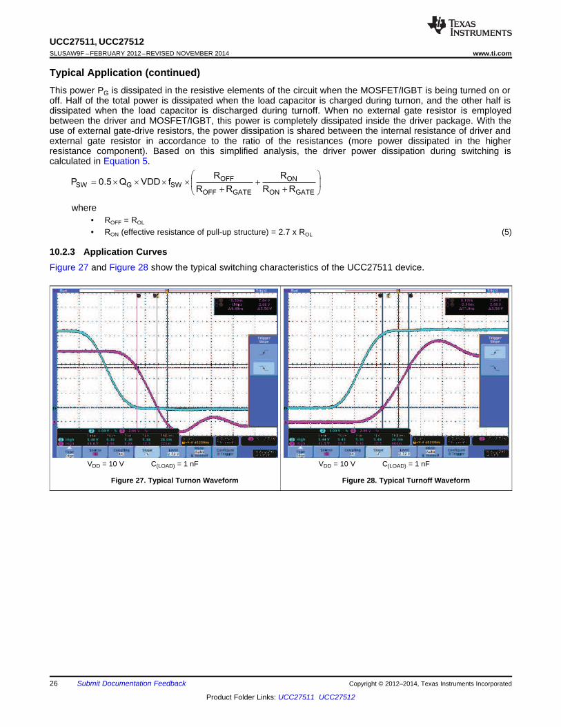
10.2.3 Application CurvesFigure 27 and Figure 28 show the typical switching characteristics of the UCC27511 device.
VDD = 10 V C(LOAD) = 1 nF VDD = 10 V C(LOAD) = 1 nF
Figure 27. Typical Turnon Waveform Figure 28. Typical Turnoff Waveform
26 Submit Documentation Feedback Copyright © 2012–2014, Texas Instruments Incorporated
Product Folder Links: UCC27511 UCC27512
UCC27511, UCC27512www.ti.com SLUSAW9F –FEBRUARY 2012–REVISED NOVEMBER 2014
11 Power Supply RecommendationsThe bias supply voltage range for which the UCC27511 and UCC27512 device is rated to operate is from 4.5 Vto 18 V. The lower end of this range is governed by the internal undervoltage-lockout (UVLO) protection featureon the VDD pin supply circuit blocks. Whenever the driver is in UVLO condition when the VDD pin voltage is belowthe V(ON) supply start threshold, this feature holds the output low, regardless of the status of the inputs. Theupper end of this range is driven by the 20-V absolute maximum voltage rating of the VDD pin of the device(which is a stress rating). Keeping a 2-V margin to allow for transient voltage spikes, the maximumrecommended voltage for the VDD pin is 18 V.
The UVLO protection feature also involves a hysteresis function. This means that when the VDD pin bias voltagehas exceeded the threshold voltage and device begins to operate, and if the voltage drops, then the devicecontinues to deliver normal functionality unless the voltage drop exceeds the hysteresis specification VDD(hys).Therefore, ensuring that, while operating at or near the 4.5 V range, the voltage ripple on the auxiliary powersupply output is smaller than the hysteresis specification of the device is important to avoid triggering deviceshutdown.
During system shutdown, the device operation continues until the VDD pin voltage has dropped below the V(OFF)threshold which must be accounted for while evaluating system shutdown timing design requirements. Likewise,at system startup, the device does not begin operation until the VDD pin voltage has exceeded above the V(ON)threshold.
The quiescent current consumed by the internal circuit blocks of the device is supplied through the VDD pin.Although this fact is well known, recognizing that the charge for source current pulses delivered by the OUTH pinis also supplied through the same VDD pin is important. As a result, every time a current is sourced out of theoutput pins (OUTH), a corresponding current pulse is delivered into the device through the VDD pin. Thusensuring that local bypass capacitors are provided between the VDD and GND pins and located as close to thedevice as possible for the purpose of decoupling is important. A low ESR, ceramic surface mount capacitor is amust. TI recommends to have 2 capacitors; a 100-nF ceramic surface-mount capacitor which can be nudgedvery close to the pins of the device and another surface-mount capacitor of few microfarads added in parallel.
12 Layout
12.1 Layout GuidelinesProper PCB layout is extremely important in a high-current fast-switching circuit to provide appropriate deviceoperation and design robustness. The UCC27511 and UCC27512 gate driver incorporates short-propagationdelays and powerful output stages capable of delivering large current peaks with very fast rise and fall times atthe gate of power switch to facilitate voltage transitions very quickly. At higher VDD voltages, the peak-currentcapability is even higher (4-A/8-A peak current is at VDD = 12 V). Very high di/dt causes unacceptable ringing ifthe trace lengths and impedances are not well controlled. The following circuit-layout guidelines are stronglyrecommended when designing with these high-speed drivers.• Locate the driver device as close as possible to power device in order to minimize the length of high-current
traces between the output pins and the gate of the power device.• Locate the VDD-bypass capacitors between VDD and GND as close as possible to the driver with minimal trace
length to improve the noise filtering. These capacitors support high-peak current being drawn from VDD duringturnon of power MOSFET. The use of low inductance SMD components such as chip resistors and chipcapacitors is highly recommended.
• The turnon and turnoff current-loop paths (driver device, power MOSFET and VDD bypass capacitor) shouldbe minimized as much as possible in order to keep the stray inductance to a minimum. High dI/dt isestablished in these loops at two instances – during turnon and turnoff transients, which will induce significantvoltage transients on the output pin of the driver device and gate of the power switch.
• Wherever possible, parallel the source and return traces, taking advantage of flux cancellation.• Separate power traces and signal traces, such as output and input signals.• Star-point grounding is a good way to minimize noise coupling from one current loop to another. The GND of
the driver should be connected to the other circuit nodes such as source of power switch, ground of PWMcontroller, and so forth, at one, single point. The connected paths should be as short as possible to reduceinductance and be as wide as possible to reduce resistance.
• Use a ground plane to provide noise shielding. Fast rise and fall times at OUT may corrupt the input signals
Copyright © 2012–2014, Texas Instruments Incorporated Submit Documentation Feedback 27
Product Folder Links: UCC27511 UCC27512
UCC27511, UCC27512SLUSAW9F –FEBRUARY 2012–REVISED NOVEMBER 2014 www.ti.com
Layout Guidelines (continued)during transition. The ground plane must not be a conduction path for any current loop. Instead the groundplane must be connected to the star-point with one single trace to establish the ground potential. In additionto noise shielding, the ground plane can help in power dissipation as well.
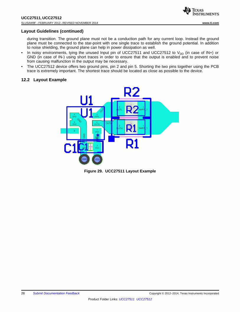
• In noisy environments, tying the unused Input pin of UCC27511 and UCC27512 to VDD (in case of IN+) orGND (in case of IN-) using short traces in order to ensure that the output is enabled and to prevent noisefrom causing malfunction in the output may be necessary.
• The UCC27512 device offers two ground pins, pin 2 and pin 5. Shorting the two pins together using the PCBtrace is extremely important. The shortest trace should be located as close as possible to the device.
12.2 Layout Example
Figure 29. UCC27511 Layout Example
28 Submit Documentation Feedback Copyright © 2012–2014, Texas Instruments Incorporated
Product Folder Links: UCC27511 UCC27512
UCC27511, UCC27512www.ti.com SLUSAW9F –FEBRUARY 2012–REVISED NOVEMBER 2014
13 Device and Documentation Support
13.1 Related LinksThe table below lists quick access links. Categories include technical documents, support and communityresources, tools and software, and quick access to sample or buy.
Table 4. Related LinksTECHNICAL TOOLS & SUPPORT &PARTS PRODUCT FOLDER SAMPLE & BUY DOCUMENTS SOFTWARE COMMUNITY
UCC27511 Click here Click here Click here Click here Click hereUCC27512 Click here Click here Click here Click here Click here
13.2 TrademarksAll trademarks are the property of their respective owners.
13.3 Electrostatic Discharge CautionThese devices have limited built-in ESD protection. The leads should be shorted together or the device placed in conductive foamduring storage or handling to prevent electrostatic damage to the MOS gates.
13.4 GlossarySLYZ022 — TI Glossary.
This glossary lists and explains terms, acronyms, and definitions.
14 Mechanical, Packaging, and Orderable InformationThe following pages include mechanical, packaging, and orderable information. This information is the mostcurrent data available for the designated devices. This data is subject to change without notice and revision ofthis document. For browser-based versions of this data sheet, refer to the left-hand navigation.
Copyright © 2012–2014, Texas Instruments Incorporated Submit Documentation Feedback 29
Product Folder Links: UCC27511 UCC27512
PACKAGE OPTION ADDENDUM
www.ti.com 9-Dec-2013
Addendum-Page 1
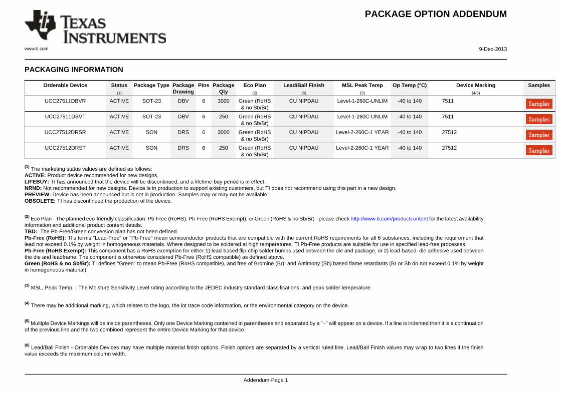
PACKAGING INFORMATION
Orderable Device Status(1)
Package Type PackageDrawing
Pins PackageQty
Eco Plan(2)
Lead/Ball Finish(6)
MSL Peak Temp(3)
Op Temp (°C) Device Marking(4/5)
Samples
UCC27511DBVR ACTIVE SOT-23 DBV 6 3000 Green (RoHS& no Sb/Br)
CU NIPDAU Level-1-260C-UNLIM -40 to 140 7511
UCC27511DBVT ACTIVE SOT-23 DBV 6 250 Green (RoHS& no Sb/Br)
CU NIPDAU Level-1-260C-UNLIM -40 to 140 7511
UCC27512DRSR ACTIVE SON DRS 6 3000 Green (RoHS& no Sb/Br)
CU NIPDAU Level-2-260C-1 YEAR -40 to 140 27512
UCC27512DRST ACTIVE SON DRS 6 250 Green (RoHS& no Sb/Br)
CU NIPDAU Level-2-260C-1 YEAR -40 to 140 27512
(1) The marketing status values are defined as follows:ACTIVE: Product device recommended for new designs.LIFEBUY: TI has announced that the device will be discontinued, and a lifetime-buy period is in effect.NRND: Not recommended for new designs. Device is in production to support existing customers, but TI does not recommend using this part in a new design.PREVIEW: Device has been announced but is not in production. Samples may or may not be available.OBSOLETE: TI has discontinued the production of the device.
(2) Eco Plan - The planned eco-friendly classification: Pb-Free (RoHS), Pb-Free (RoHS Exempt), or Green (RoHS & no Sb/Br) - please check http://www.ti.com/productcontent for the latest availabilityinformation and additional product content details.TBD: The Pb-Free/Green conversion plan has not been defined.Pb-Free (RoHS): TI's terms "Lead-Free" or "Pb-Free" mean semiconductor products that are compatible with the current RoHS requirements for all 6 substances, including the requirement thatlead not exceed 0.1% by weight in homogeneous materials. Where designed to be soldered at high temperatures, TI Pb-Free products are suitable for use in specified lead-free processes.Pb-Free (RoHS Exempt): This component has a RoHS exemption for either 1) lead-based flip-chip solder bumps used between the die and package, or 2) lead-based die adhesive used betweenthe die and leadframe. The component is otherwise considered Pb-Free (RoHS compatible) as defined above.Green (RoHS & no Sb/Br): TI defines "Green" to mean Pb-Free (RoHS compatible), and free of Bromine (Br) and Antimony (Sb) based flame retardants (Br or Sb do not exceed 0.1% by weightin homogeneous material)
(3) MSL, Peak Temp. - The Moisture Sensitivity Level rating according to the JEDEC industry standard classifications, and peak solder temperature.
(4) There may be additional marking, which relates to the logo, the lot trace code information, or the environmental category on the device.
(5) Multiple Device Markings will be inside parentheses. Only one Device Marking contained in parentheses and separated by a "~" will appear on a device. If a line is indented then it is a continuationof the previous line and the two combined represent the entire Device Marking for that device.
(6) Lead/Ball Finish - Orderable Devices may have multiple material finish options. Finish options are separated by a vertical ruled line. Lead/Ball Finish values may wrap to two lines if the finishvalue exceeds the maximum column width.
PACKAGE OPTION ADDENDUM
www.ti.com 9-Dec-2013
Addendum-Page 2
Important Information and Disclaimer:The information provided on this page represents TI's knowledge and belief as of the date that it is provided. TI bases its knowledge and belief on informationprovided by third parties, and makes no representation or warranty as to the accuracy of such information. Efforts are underway to better integrate information from third parties. TI has taken andcontinues to take reasonable steps to provide representative and accurate information but may not have conducted destructive testing or chemical analysis on incoming materials and chemicals.TI and TI suppliers consider certain information to be proprietary, and thus CAS numbers and other limited information may not be available for release.
In no event shall TI's liability arising out of such information exceed the total purchase price of the TI part(s) at issue in this document sold by TI to Customer on an annual basis.
OTHER QUALIFIED VERSIONS OF UCC27512 :
• Enhanced Product: UCC27512-EP
NOTE: Qualified Version Definitions:
• Enhanced Product - Supports Defense, Aerospace and Medical Applications
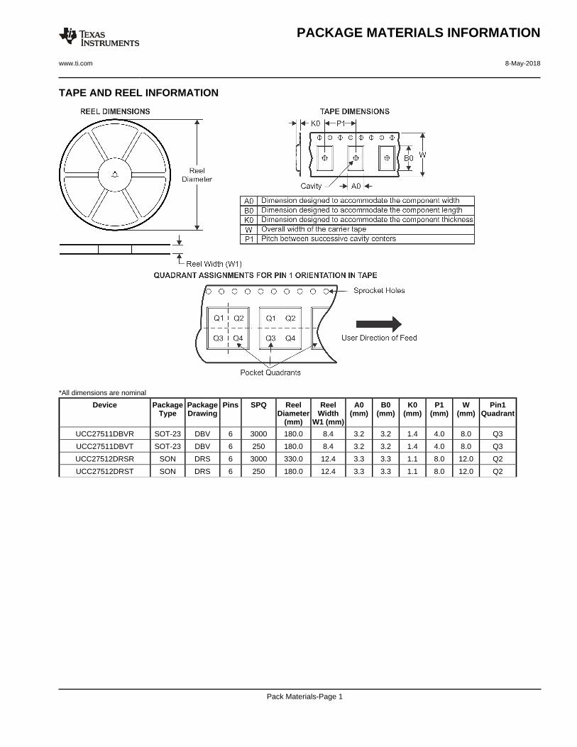
TAPE AND REEL INFORMATION
*All dimensions are nominal
Device PackageType
PackageDrawing
Pins SPQ ReelDiameter
(mm)
ReelWidth
W1 (mm)
A0(mm)
B0(mm)
K0(mm)
P1(mm)
W(mm)
Pin1Quadrant
UCC27511DBVR SOT-23 DBV 6 3000 180.0 8.4 3.2 3.2 1.4 4.0 8.0 Q3
UCC27511DBVT SOT-23 DBV 6 250 180.0 8.4 3.2 3.2 1.4 4.0 8.0 Q3
UCC27512DRSR SON DRS 6 3000 330.0 12.4 3.3 3.3 1.1 8.0 12.0 Q2
UCC27512DRST SON DRS 6 250 180.0 12.4 3.3 3.3 1.1 8.0 12.0 Q2
PACKAGE MATERIALS INFORMATION
www.ti.com 8-May-2018
Pack Materials-Page 1
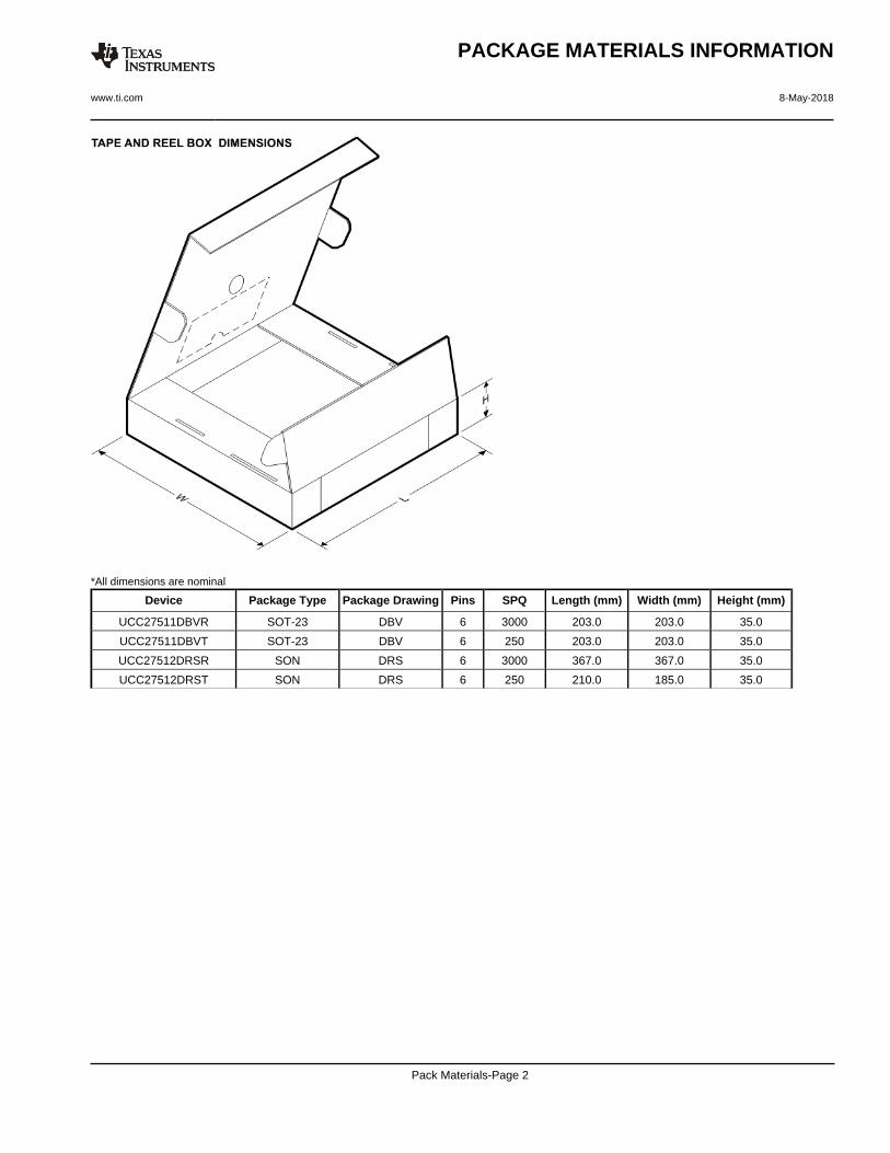
*All dimensions are nominal
Device Package Type Package Drawing Pins SPQ Length (mm) Width (mm) Height (mm)
UCC27511DBVR SOT-23 DBV 6 3000 203.0 203.0 35.0
UCC27511DBVT SOT-23 DBV 6 250 203.0 203.0 35.0
UCC27512DRSR SON DRS 6 3000 367.0 367.0 35.0
UCC27512DRST SON DRS 6 250 210.0 185.0 35.0
PACKAGE MATERIALS INFORMATION
www.ti.com 8-May-2018
Pack Materials-Page 2
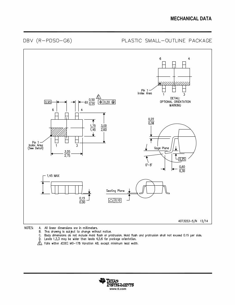
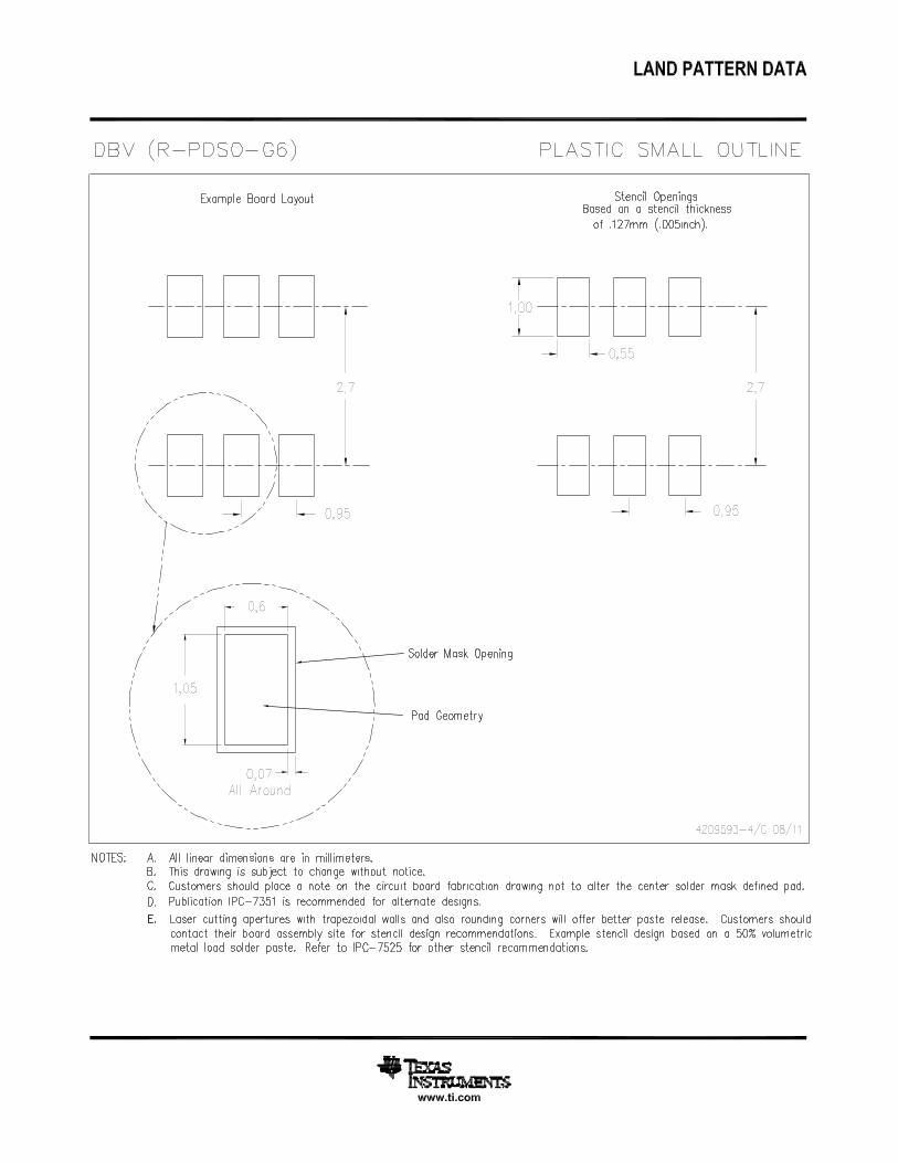
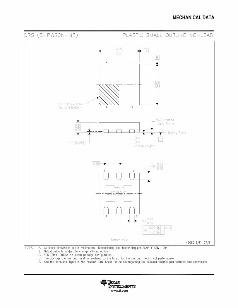
IMPORTANT NOTICE
Texas Instruments Incorporated (TI) reserves the right to make corrections, enhancements, improvements and other changes to itssemiconductor products and services per JESD46, latest issue, and to discontinue any product or service per JESD48, latest issue. Buyersshould obtain the latest relevant information before placing orders and should verify that such information is current and complete.TI’s published terms of sale for semiconductor products (http://www.ti.com/sc/docs/stdterms.htm) apply to the sale of packaged integratedcircuit products that TI has qualified and released to market. Additional terms may apply to the use or sale of other types of TI products andservices.Reproduction of significant portions of TI information in TI data sheets is permissible only if reproduction is without alteration and isaccompanied by all associated warranties, conditions, limitations, and notices. TI is not responsible or liable for such reproduceddocumentation. Information of third parties may be subject to additional restrictions. Resale of TI products or services with statementsdifferent from or beyond the parameters stated by TI for that product or service voids all express and any implied warranties for theassociated TI product or service and is an unfair and deceptive business practice. TI is not responsible or liable for any such statements.Buyers and others who are developing systems that incorporate TI products (collectively, “Designers”) understand and agree that Designersremain responsible for using their independent analysis, evaluation and judgment in designing their applications and that Designers havefull and exclusive responsibility to assure the safety of Designers' applications and compliance of their applications (and of all TI productsused in or for Designers’ applications) with all applicable regulations, laws and other applicable requirements. Designer represents that, withrespect to their applications, Designer has all the necessary expertise to create and implement safeguards that (1) anticipate dangerousconsequences of failures, (2) monitor failures and their consequences, and (3) lessen the likelihood of failures that might cause harm andtake appropriate actions. Designer agrees that prior to using or distributing any applications that include TI products, Designer willthoroughly test such applications and the functionality of such TI products as used in such applications.TI’s provision of technical, application or other design advice, quality characterization, reliability data or other services or information,including, but not limited to, reference designs and materials relating to evaluation modules, (collectively, “TI Resources”) are intended toassist designers who are developing applications that incorporate TI products; by downloading, accessing or using TI Resources in anyway, Designer (individually or, if Designer is acting on behalf of a company, Designer’s company) agrees to use any particular TI Resourcesolely for this purpose and subject to the terms of this Notice.TI’s provision of TI Resources does not expand or otherwise alter TI’s applicable published warranties or warranty disclaimers for TIproducts, and no additional obligations or liabilities arise from TI providing such TI Resources. TI reserves the right to make corrections,enhancements, improvements and other changes to its TI Resources. TI has not conducted any testing other than that specificallydescribed in the published documentation for a particular TI Resource.Designer is authorized to use, copy and modify any individual TI Resource only in connection with the development of applications thatinclude the TI product(s) identified in such TI Resource. NO OTHER LICENSE, EXPRESS OR IMPLIED, BY ESTOPPEL OR OTHERWISETO ANY OTHER TI INTELLECTUAL PROPERTY RIGHT, AND NO LICENSE TO ANY TECHNOLOGY OR INTELLECTUAL PROPERTYRIGHT OF TI OR ANY THIRD PARTY IS GRANTED HEREIN, including but not limited to any patent right, copyright, mask work right, orother intellectual property right relating to any combination, machine, or process in which TI products or services are used. Informationregarding or referencing third-party products or services does not constitute a license to use such products or services, or a warranty orendorsement thereof. Use of TI Resources may require a license from a third party under the patents or other intellectual property of thethird party, or a license from TI under the patents or other intellectual property of TI.TI RESOURCES ARE PROVIDED “AS IS” AND WITH ALL FAULTS. TI DISCLAIMS ALL OTHER WARRANTIES ORREPRESENTATIONS, EXPRESS OR IMPLIED, REGARDING RESOURCES OR USE THEREOF, INCLUDING BUT NOT LIMITED TOACCURACY OR COMPLETENESS, TITLE, ANY EPIDEMIC FAILURE WARRANTY AND ANY IMPLIED WARRANTIES OFMERCHANTABILITY, FITNESS FOR A PARTICULAR PURPOSE, AND NON-INFRINGEMENT OF ANY THIRD PARTY INTELLECTUALPROPERTY RIGHTS. TI SHALL NOT BE LIABLE FOR AND SHALL NOT DEFEND OR INDEMNIFY DESIGNER AGAINST ANY CLAIM,INCLUDING BUT NOT LIMITED TO ANY INFRINGEMENT CLAIM THAT RELATES TO OR IS BASED ON ANY COMBINATION OFPRODUCTS EVEN IF DESCRIBED IN TI RESOURCES OR OTHERWISE. IN NO EVENT SHALL TI BE LIABLE FOR ANY ACTUAL,DIRECT, SPECIAL, COLLATERAL, INDIRECT, PUNITIVE, INCIDENTAL, CONSEQUENTIAL OR EXEMPLARY DAMAGES INCONNECTION WITH OR ARISING OUT OF TI RESOURCES OR USE THEREOF, AND REGARDLESS OF WHETHER TI HAS BEENADVISED OF THE POSSIBILITY OF SUCH DAMAGES.Unless TI has explicitly designated an individual product as meeting the requirements of a particular industry standard (e.g., ISO/TS 16949and ISO 26262), TI is not responsible for any failure to meet such industry standard requirements.Where TI specifically promotes products as facilitating functional safety or as compliant with industry functional safety standards, suchproducts are intended to help enable customers to design and create their own applications that meet applicable functional safety standardsand requirements. Using products in an application does not by itself establish any safety features in the application. Designers mustensure compliance with safety-related requirements and standards applicable to their applications. Designer may not use any TI products inlife-critical medical equipment unless authorized officers of the parties have executed a special contract specifically governing such use.Life-critical medical equipment is medical equipment where failure of such equipment would cause serious bodily injury or death (e.g., lifesupport, pacemakers, defibrillators, heart pumps, neurostimulators, and implantables). Such equipment includes, without limitation, allmedical devices identified by the U.S. Food and Drug Administration as Class III devices and equivalent classifications outside the U.S.TI may expressly designate certain products as completing a particular qualification (e.g., Q100, Military Grade, or Enhanced Product).Designers agree that it has the necessary expertise to select the product with the appropriate qualification designation for their applicationsand that proper product selection is at Designers’ own risk. Designers are solely responsible for compliance with all legal and regulatoryrequirements in connection with such selection.Designer will fully indemnify TI and its representatives against any damages, costs, losses, and/or liabilities arising out of Designer’s non-compliance with the terms and provisions of this Notice.
Mailing Address: Texas Instruments, Post Office Box 655303, Dallas, Texas 75265Copyright © 2018, Texas Instruments Incorporated