Embed Size (px)
Citation preview

DISPLAY MODULE
SXGA+ Resolution
TCONw/ LVDS Interface
24-bit RGB4 Control
Clock1.8V
LVCMOS
FPD-Link4D+C LVDS
LVDS0+/-
LVDS1+/-
LVDS2+/-
LVDSC+/-
LVDS3+/-
R7-R0
G7-G0
B7-B0
HSyncVSync
DE
CLK
GPO/CNTL(L/R)
PDB
1.8V
DS90C185FPD-Link
SERIALIZER
GPU
DS90C185
www.ti.com SNLS402D –FEBRUARY 2012–REVISED FEBRUARY 2013
DS90C185 Low Power 1.8V FPD-Link (LVDS) SerializerCheck for Samples: DS90C185
1FEATURES DESCRIPTIONThe DS90C185 is a low-power serializer for portable
2• Typical power 50 mW at 75-MHz pclkbattery-powered applications that reduces the size of
• Drives up to 1400x1050 at 60-Hz (SXGA+) the RGB interface between the host GPU and theDisplays display.
• 2.94 Gbps of throughput24-bit RGB plus three video control signals are
• Two operating modes: 24-bit and 18-bit RGB serialized and translated to LVDS-compatible levelsand sent as a 4 data + clock (4D+C) reduced-width• 25- to 105-MHz Pixel Clock supportLVDS compatible interface. The LVDS Interface is• Single 1.8-V Supplycompatible with FPD-Link (1) deserializers and many
• Sleep Mode LVDS based displays. These interfaces are• Spread Spectrum Clock compatibility commonly supported in LCD modules with “LVDS” or
FPD-Link / FlatLink single-pixel input interfaces.• Small 6mm x 6mm x 0.8mm WQFN packageDisplays up to 1400x1050 at 60 fps are supported
APPLICATIONS with 24-bpp color depth. 18 bpp may also besupported by a dedicated mode with a 3D+C output.• eBooksPower dissipation is minimized by the full LVCMOS
• Media Tablet Devices design and 1.8-V powered core and VDDIO rails.• Netbooks
The DS90C185 is offered in the small 48-pin WQFN• Portable Display Monitors package and features single 1.8-V supply operation
for minimum power dissipation (50 mW typ).
System Diagram
1
Please be aware that an important notice concerning availability, standard warranty, and use in critical applications ofTexas Instruments semiconductor products and disclaimers thereto appears at the end of this data sheet.
2All trademarks are the property of their respective owners.
PRODUCTION DATA information is current as of publication date. Copyright © 2012–2013, Texas Instruments IncorporatedProducts conform to specifications per the terms of the TexasInstruments standard warranty. Production processing does notnecessarily include testing of all parameters.

1
2
3
4
5
6
7
8
9
10
11
12
48 47 46 45 44 43 42 41 40 39 38 37
36
35
34
33
32
31
30
29
28
27
26
25
13 14 15 16 17 18 19 20 21 22 23 24
DS90C185SQTOP VIEW
DAP = GND
(Not to scale)
VD
D
D8
D7
D6
D5
D4
D3
D2
D1
D0
VO
D_S
EL
PD
B
D9
D10
D11
D12
CLK
D13
D19
D14
D15
D16
D17
D18
GN
D
D20
D21
D22
D23
D24
VD
DP
LL
D25
D26
D27
RF
B
GN
D
18B_MODE
TxOUT0-
TxOUT0+
TxOUT1-
TxOUT1+
TxOUT2-
TxOUT2+
TxCLKOUT-
TxCLKOUT+
TxOUT3-
TxOUT3+
VDDTX
PDB
CLK
LVC
MO
S P
AR
ALL
EL
TO
LV
DS
PLL
RED
GREEN
BLUE
HS
VS
DECNTRL (L/R)
D0 ± D27
LVCMOS INPUTS
DATA (LVDS)
CLOCK (LVDS)
18B_Mode
VOD_SEL
RFB
DS90C185 - SERIALIZER
DS90C185
SNLS402D –FEBRUARY 2012–REVISED FEBRUARY 2013 www.ti.com
Functional Block Diagram
Connection Diagram
2 Submit Documentation Feedback Copyright © 2012–2013, Texas Instruments Incorporated
Product Folder Links: DS90C185
DS90C185
www.ti.com SNLS402D –FEBRUARY 2012–REVISED FEBRUARY 2013
Table 1. DS90C185 Pin Descriptions
Pin Name I/O No. Description
1.8 V LVCMOS VIDEO INPUTS
D27-D21, I 22-16, Data input pins.D20, 14, This includes: 8 Red, 8 Green, 8 Blue, and 3 video control lines and a general purpose or L/RD19-D14, 12-7, control bit. Includes pull down.D13-D9, 5-1,D8-D1, 47-40,D0 38
CLK I 6 Clock input.Includes pull down.
LVDS VIDEO OUTPUTS
TxOUT0 –/+, O 36, 35 LVDS Output Data — Expects 100 Ω DC load.TxOUT1 –/+, 34, 33TxOUT2 –/+, 32, 31TxOUT3 –/+, 28, 27
TxCLK OUT -/+ O 30, 29 LVDS Output Clock — Expects 100 Ω DC load.
1.8 V LVCMOS CONTROL INPUTS
R_FB I 23 LVCMOS Ievel programmable strobe select1 = Rising Edge Clock0 = Falling Edge Clock — defaultIncludes pull down.
18B_Mode I 26 Mode Configuration Input1 = 3D+C (18 bit RGB mode)0 = 4D+C (24 bit RGB mode) — defaultIncludes pull down.
VOD_SEL I 39 VOD Select Input0 = Reduced VOD (lower power)1 = Normal VOD — defaultIncludes pull down.
PDB I 37 Power Down Bar(Sleep) Input1 = ACTIVE0 = Sleep State (low power idle) — defaultIncludes pull down.
POWER and GROUND
VDD P 48 Digital power input
VDDTX P 25 LVDS driver power input
VDDPLL P 13 PLL power input
GND G 15, 24 Ground pins
DAP G Connect DAP to ground plane
These devices have limited built-in ESD protection. The leads should be shorted together or the device placed in conductive foamduring storage or handling to prevent electrostatic damage to the MOS gates.
Copyright © 2012–2013, Texas Instruments Incorporated Submit Documentation Feedback 3
Product Folder Links: DS90C185

DS90C185
SNLS402D –FEBRUARY 2012–REVISED FEBRUARY 2013 www.ti.com
Absolute Maximum Ratings (1)
Supply Voltage (VDD) −0.3V to +2.5V
LVCMOS Input Voltage −0.5V to (VDD + 0.3V)
LVDS Driver Output Voltage −0.3V to (VDD + 0.3V)
LVDS Output Short CircuitDuration Continuous
Junction Temperature +150°C
Storage Temperature −65°C to +150°C
Lead Temperature (Soldering, 4 sec) +260°C
Package Derating: θJA 26.6 °C/W above +22°C
ESD Ratings
HBM >4kV
CDM >1.25kV
MM >250V
(1) “Absolute Maximum Ratings” are those values beyond which the safety of the device cannot be guaranteed. They are not meant toimply that the device should be operated at these limits. The tables of “Electrical Characteristics” specify conditions for device operation.
Recommended OperatingConditionsMin Nom Max Units
Supply Voltage (VDD) 1.71 1.8 1.89 V
Operating Free Air Temperature (TA) −10 +22 +70 °C
Supply Noise Voltage (VDD) <90 mVPP
Differential Load Impedance 80 100 120 ΩInput Clock Frequency 25 105 MHz
4 Submit Documentation Feedback Copyright © 2012–2013, Texas Instruments Incorporated
Product Folder Links: DS90C185

DS90C185
www.ti.com SNLS402D –FEBRUARY 2012–REVISED FEBRUARY 2013
Electrical CharacteristicsOver recommended operating supply and temperature ranges unless otherwise specified.
Symbol Parameter Conditions Min Typ Max Units
LVCMOS DC SPECIFICATIONS
VIH High Level Input Voltage 0.65 VDD VVDD
VIL Low Level Input Voltage GND 0.35 VVDD
IIN Input Current VIN = 0V or VDD = 1.71 V to 1.89 V –10 ±1 +10 μA
LVDS DC SPECIFICATIONS
VOD Differential Output Voltage RL = 100Ω VODSEL = H 160 300 450 mVFigure 3 (320) (600) (900) (mVP-P)
VODSEL = L 115 180 300 mV(230) (360) (600) (mVP-P)
ΔVOD Change in VOD between complimentary RL = 100Ω 50 mVoutput states
VOS Offset Voltage 0.8 0.9 1.0 V
ΔVOS Change in VOS between complimentary 50 mVoutput states
IOS Output Short Circuit Current VOUT = 0V, RL = 100Ω –45 −35 −25 mA
IOZ Output LVDS Driver Power Down Current PDB = 0V ±1 ±10 mA
SERIALIZER SUPPLY CURRENT
IDDT1 Serializer Supply Current Checkerboard pattern, f = 105 MHz 60 85 mAWorst Case RL = 100Ω,
18B_MODE = L,VOD_SEL = H,VDD = 1.89Figure 1
IDDTG Serializer Supply Current RL = 100Ω, f = 75 MHz 31 mA16 Grayscale 18B_MODE = L,
VOD_SEL = L,VDD = 1.816 Grayscale Pattern
RL = 100Ω, 41 mA18B_MODE = L,VOD_SEL = H,VDD = 1.816 Grayscale Pattern
RL = 100Ω, 28 mA18B_MODE = H,VOD_SEL = L,VDD = 1.816 Grayscale Pattern
RL = 100Ω, 36 mA18B_MODE = H,VOD_SEL = H,VDD = 1.816 Grayscale Pattern
Copyright © 2012–2013, Texas Instruments Incorporated Submit Documentation Feedback 5
Product Folder Links: DS90C185

DS90C185
SNLS402D –FEBRUARY 2012–REVISED FEBRUARY 2013 www.ti.com
Electrical Characteristics (continued)Over recommended operating supply and temperature ranges unless otherwise specified.
Symbol Parameter Conditions Min Typ Max Units
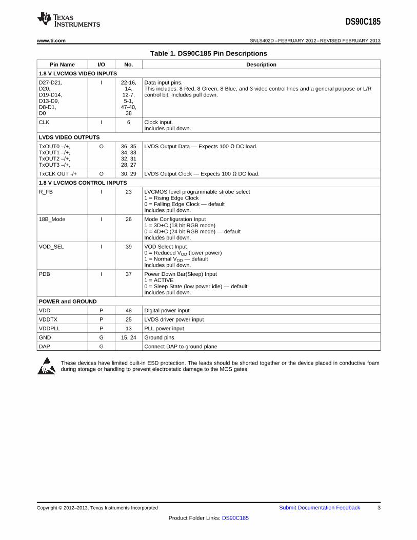
IDDTP Serializer Supply Current RL = 100Ω, f = 75 MHz 33 mAPRBS-7 18B_MODE = L, Figure 11
VOD_SEL = L,VDD = 1.8PRBS-7 Pattern
RL = 100Ω, 45 mA18B_MODE = L,VOD_SEL = H,VDD = 1.8PRBS-7 Pattern
RL = 100Ω, 29 mA18B_MODE = H,VOD_SEL = L,VDD = 1.8PRBS-7 Pattern
RL = 100Ω, 38 mA18B_MODE = H,VOD_SEL = H,VDD = 1.8PRBS-7 Pattern
IDDZ Serializer Power Down Current 18 200 μA
6 Submit Documentation Feedback Copyright © 2012–2013, Texas Instruments Incorporated
Product Folder Links: DS90C185

DS90C185
www.ti.com SNLS402D –FEBRUARY 2012–REVISED FEBRUARY 2013
Recommended Transmitter Input CharacteristicsOver recommended operating supply and temperature ranges unless otherwise specified
Symbol Parameter Min Typ Max Units
TCIT TxCLK IN Transition Time (Figure 5) 1.0 6.0 ns
TCIP TxCLK IN Period (Figure 6) 9.52 T 40 ns
TCIH TxCLK IN High Time (Figure 6) 0.35T 0.5T 0.65T ns
TCIL TxCLK IN Low Time (Figure 6) 0.35T 0.5T 0.65T ns
Transmitter Switching CharacteristicsOver recommended operating supply and temperature ranges unless otherwise specified
Symbol Parameter Min Typ Max Units
LLHT LVDS Low-to-High Transition Time (Figure 4 (1)) 0.18 0.5 ns
LHLT LVDS High-to-Low Transition Time (Figure 4 (1)) 0.18 0.5 ns
TPPOS0 Transmitter Output Pulse Positions Normalized for Bit f = 105 MHz 1 UI0 Figure 10
TPPOS1 Transmitter Output Pulse Positions Normalized for Bit 2 UI1
TPPOS2 Transmitter Output Pulse Positions Normalized for Bit 3 UI2
TPPOS3 Transmitter Output Pulse Positions Normalized for Bit 4 UI3
TPPOS4 Transmitter Output Pulse Positions Normalized for Bit 5 UI4
TPPOS5 Transmitter Output Pulse Positions Normalized for Bit 6 UI5
TPPOS6 Transmitter Output Pulse Positions Normalized for Bit 7 UI6
ΔTPPOS Variation in Transmitter Pulse Position (Bit 6 — Bit 0) ±0.06 UI
TSTC Required TxIN Setup to TxCLK IN Figure 6 0 ns
THTC Required TxIN Hold to TxCLK IN 2.5 ns
TCCJ Cycle to Cycle Jitter f = 105 MHz (1) 0.028 0.035 UI
TSD f = 105 MHz 2*TCIP + 2*TCIP + nsSerializer Propagation Delay Figure 7 10.54 13.96
TCCS TxOUT Channel to Channel Skew 110 ps
TPLLS Transmitter Phase Lock Loop Set Figure 8 1 ms
TPPD Transmitter Power Down Delay Figure 9 (2) 100 ns
(1) Parameter is guaranteed by characterization and is not tested at final test.(2) Parameter is guaranteed by design and is not tested at final test.
Copyright © 2012–2013, Texas Instruments Incorporated Submit Documentation Feedback 7
Product Folder Links: DS90C185

f
f / 16
f / 8
f / 4
f / 2
Steady State, Low
Steady State, Low
f / 16
f / 8
f / 4
f / 2
Steady State, Low
Steady State, Low
f / 16
f / 8
f / 4
f / 2
Steady State, Low
Steady State, Low
Steady State, High
Steady State, High
Steady State, High
PCLK
R0
R1
R2
R3
R4
R5
G0
G1
G2
G3
G4
G5
B0
B1
B2
B3
B4
B5
HS
VS
DE
Signal Signal Pattern Signal Frequency
T
CLK
Dx, x = ODD
Dx, x = EVEN
Falling Edge CLK (RFB = GND) shown
DS90C185
SNLS402D –FEBRUARY 2012–REVISED FEBRUARY 2013 www.ti.com
AC Timing Diagrams
NOTE: The worst case test pattern produces a maximum toggling of digital circuits, LVDS I/O and LVCMOS I/O.
Figure 1. “Worst Case” Test Pattern
NOTE: Recommended pin to signal mapping for 18 bits per pixel, customer may choose to define differently. The 16grayscale test pattern tests device power consumption for a “typical” LCD display pattern. The test patternapproximates signal switching needed to produce groups of 16 vertical stripes across the display.
NOTE: Figure 1 and Figure 2 show a falling edge data strobe (CLK).
Figure 2. “16 Grayscale” Test Pattern - DS90C185
Figure 3. DS90C185 (Transmitter) LVDS Output Load
8 Submit Documentation Feedback Copyright © 2012–2013, Texas Instruments Incorporated
Product Folder Links: DS90C185

Pixel n Pixel n+1 Pixel n+2 Pixel n+3
Pixel n Pixel n+1TxOUTn+/-
TxCLKOUT+/-
TSD
CLK
D0 ± D27 Pixel n-1
50%
50%
VDD
VDD
GND
GND
TSTC THTC
VIHmin
VILmax
TCIP TCIH TCIL
Falling Edge CLK shown (RFB = GND)
TCIT TCIT
80%
20%
80%
20%
50%
GND
VDD
DS90C185
www.ti.com SNLS402D –FEBRUARY 2012–REVISED FEBRUARY 2013
AC Timing Diagrams (continued)
Figure 4. DS90C185 (Transmitter) LVDS Transition Times
Figure 5. DS90C185 (Transmitter) Input Clock Transition Time
Figure 6. DS90C185 (Transmitter) Setup/Hold and High/Low Times with R_FB pin = GND (Falling EdgeStrobe)
Figure 7. DS90C185 Propagation Delay
Copyright © 2012–2013, Texas Instruments Incorporated Submit Documentation Feedback 9
Product Folder Links: DS90C185
20 40 60 80 100 120
20
25
30
35
40
45
50
55
60
IDD
(m
A)
FREQUENCY (MHz)
VODSEL = L, 18B = LVODSEL = H, 18B = LVODSEL = L, 18B = HVODSEL = H, 18B = H
bit 1n-1
bit 0n-1
bit 6n
bit 5n
bit 4n
bit 3n
bit 2n
bit 1n
bit 0n
Cycle N
1UI
2UI
3UI
4UI
5UI
6UI
7UI
TxCLKOUT
TxOUT[3:0]+/-
PDB
CLK
TxCLKOUT(Diff.)
VDD
GND
(LVDS)
GND
VDD
TPDD
50%
VDD
PDB
CLK
TxCLKOUT(Diff.)
1.8V
VDD
GND
(LVDS)
GND
VDD
GND
TPLLS
DS90C185
SNLS402D –FEBRUARY 2012–REVISED FEBRUARY 2013 www.ti.com
AC Timing Diagrams (continued)
Figure 8. DS90C185 (Transmitter) Phase Lock Loop Set Time
Figure 9. Transmitter Power Down Delay
Figure 10. Transmitter LVDS Output Pulse Position Measurement - DS90C185
Figure 11. Typ Current Draw — PRBS-7 Data Pattern
10 Submit Documentation Feedback Copyright © 2012–2013, Texas Instruments Incorporated
Product Folder Links: DS90C185

D27 D26 D25 D24 D23 D22 D21
D20 D19 D18 D17 D16 D15 D14
D13 D12 D11 D10 D9 D8 D7
D6 D5 D4 D3 D2 D1 D0
TxCLKOUT+/-(Diff)
TxOUT3+/-(SE)
TxOUT2+/-(SE)
TxOUT1+/-(SE)
TxOUT0+/-(SE)
Current Cycle
TRI-STATE
D20 D19 D18 D17 D16 D15 D14
D13 D12 D11 D10 D9 D8 D7
D6 D5 D4 D3 D2 D1 D0
TxCLKOUT+/-(Diff)
TxOUT3+/-(SE)
TxOUT2+/-(SE)
TxOUT1+/-(SE)
TxOUT0+/-(SE)
Current Cycle
DS90C185
www.ti.com SNLS402D –FEBRUARY 2012–REVISED FEBRUARY 2013
LVDS INTERFACE, TFT COLOR DATA RECOMMENDED MAPPING
Different color mapping options exist. Check with the color mapping of the Deserializer / TCON device that isused to ensure compatible mapping for the application. The DS90C185 supports single pixel interfaces witheither 24bpp or 18bpp color depths.
The DS90C185 provides four LVDS data lines along with an LVDS clock line (4D+C) for the 28 LVCMOS datainputs. The 28 bit interface typically assigns 24 bits to RGB color data, 3 bits to video control (HS, VS and DE)and one spare bit can be ignored, used for L/R signaling or function as a general purpose bit. The single pixel24bpp 4D+C LVDS interface mapping is shown Figure 13. A single pixel 18bpp mode is also supported byutilizing the 18B_MODE pin. In this configuration the TxOUT3 output channel is place in TRI-STATE® to savepower. Its respective inputs are ignored. This mapping is shown in Figure 12.
Figure 12. DS90C185 LVDS Map — 18B_MODE = H
Figure 13. DS90C185 LVDS Map — 18B_MODE = L
COLOR MAPPING INFORMATION
A defacto color mapping is shown next. Different color mapping options exist. Check with the color mapping ofthe Deserializer / TCON device that is used to ensure compatible mapping for the application.
Table 2. 24bpp / MSB on CH3
DS90C187 Input Color Mapping Note
D22 R7 MSB
D21 R6
D5 R5
D4 R4
D3 R3
D2 R2
D1 R1
D0 R0 LSB
Copyright © 2012–2013, Texas Instruments Incorporated Submit Documentation Feedback 11
Product Folder Links: DS90C185

DS90C185
SNLS402D –FEBRUARY 2012–REVISED FEBRUARY 2013 www.ti.com
Table 2. 24bpp / MSB on CH3 (continued)
DS90C187 Input Color Mapping Note
D24 G7 MSB
D23 G6
D11 G5
D10 G4
D9 G3
D8 G2
D7 G1
D6 G0 LSB
D26 B7 MSB
D25 B6
D17 B5
D16 B4
D15 B3
D14 B2
D13 B1
D12 B0
D20 DE Data Enable
D19 VS Vertical Sync
D18 HS Horizontal Sync
D27 GP General Purpose
Table 3. 24bpp / LSB on CH3
DS90C187 Input Color Mapping Note
D5 R7 MSB
D4 R6
D3 R5
D2 R4
D1 R3
D0 R2
D22 R1
D21 R0 LSB
D11 G7 MSB
D10 G6
D9 G5
D8 G4
D7 G3
D6 G2
D24 G1
D23 G0 LSB
D17 B7 MSB
D16 B6
D15 B5
D14 B4
D13 B3
D12 B2
D26 B1
D25 B0
12 Submit Documentation Feedback Copyright © 2012–2013, Texas Instruments Incorporated
Product Folder Links: DS90C185

DS90C185
www.ti.com SNLS402D –FEBRUARY 2012–REVISED FEBRUARY 2013
Table 3. 24bpp / LSB on CH3 (continued)
DS90C187 Input Color Mapping Note
D20 DE Data Enable
D19 VS Vertical Sync
D18 HS Horizontal Sync
D27 GP General Purpose
Table 4. 18bpp
DS90C187 Input Color Mapping Note
D5 R5 MSB
D4 R4
D3 R3
D2 R2
D1 R1
D0 R0 LSB
D11 G5 MSB
D10 G4
D9 G3
D8 G2
D7 G1
D6 G0 LSB
D17 B5 MSB
D16 B4
D15 B3
D14 B2
D13 B1
D12 B0
D20 DE Data Enable
D19 VS Vertical Sync
D18 HS Horizontal Sync
FUNCTIONAL DESCRIPTION
DS90C185 converts a wide parallel LVCMOS input bus into FPD-Link LVDS data. The device can be configuredto support RGB-888 (24 bit color) or RGB-666 (18 bit color). The DS90C185 has several power saving featuresincluding: selectable VOD, 18 bit / 24 bit mode select, and a power down pin control.
In each input pixel clock cycle, data from D[27:0] is serialized and driven out on TxOUT[3:0] +/- with TxCLKOUT+/-. If 18B_MODE is LOW, then TxOUT3 +/- is powered down and the corresponding LVCMOS input signals areignored.
The input pixel clock can range from 25 MHz to 105 MHz, resulting in a total maximum payload of 700 Mbps (28bits * 25MHz) to 2.94 Gbps (28 bits * 105 MHz). Each LVDS driver will operate at a speed of 7 bits per inputclock cycle, resulting in a serial line rate of 175 Mbps to 735 Mbps. TxCLKOUT +/- will operate at the same rateas CLK with a duty cycle ratio of 57:43.
Pixel Clock Edge Select (RFB)
The RFB pin determines the edge that the input LVCMOS data is latched on. If RFB is HIGH, input data islatched on the RISING EDGE of the pixel clock (CLK). If RFB is LOW, the input data is latched on the FALLINGEDGE of the pixel clock. Note: This can be set independently of receiver’s output clock strobe.
Copyright © 2012–2013, Texas Instruments Incorporated Submit Documentation Feedback 13
Product Folder Links: DS90C185
DS90C185
SNLS402D –FEBRUARY 2012–REVISED FEBRUARY 2013 www.ti.com
Table 5. Pixel Clock Edge
RFB Result
0 FALLING edge
1 RISING edge
Power Management
The DS90C185 has several features to assist with managing power consumption. The 18B_MODE pin allows theDS90C185 to power down the unused LVDS driver for RGB-666 (18 bit color) applications. If no clock is appliedto the CLK pin, the DS90C185 will enter a low power state. To place the DS90C185 in its lowest power state, thedevice can be powered down by driving the PDB pin to LOW.
Sleep Mode (PDB)
The DS90C185 provides a power down feature. When the device has been powered down, current draw throughthe supply pins is minimized and the PLL is shut down. The LVDS drivers are also powered down with theiroutputs pulled to GND through 100Ω resistors.
Table 6. Power Down Select
PDB Result
0 SLEEP Mode (default)
1 ACTIVE (enabled)
LVDS Outputs
The DS90C185's LVDS drivers are compatible with ANSI/TIA/EIA-644–A LVDS receivers. The LVDS drivers anoutput a power saving low VOD or a higher VOD to enable longer trace and cable lengths by configuring theVODSEL pin.
Table 7. VOD Select
VODSEL Result
0 ±180 mV (360mVpp)
1 ±300 mV (600mVpp)
For more information regarding the electrical characteristics of the LVDS outputs, refer to the LVDS DCCharacteristics and LVDS Switching Specifications.
18 bit / 24 bit Color Mode (18B)
The 18B pin can be used to further save power by powering down the 4th LVDS driver in each used bank whenthe application requires only 18 bit color or 3D+C LVDS. Set the 18B pin to logic HIGH to TRI-STATE® TxOUT3+/-. For 24 bit color applications this pin should be set to logic LOW. Note that the power down function takespriority over the TRI-STATE® function.
Table 8. Color Depth Configurations
18B_Mode Result
0 24bpp, LVDS 4D+C
1 18bpp, LVDS 3D+C
LVCMOS Inputs
The DS90C185 has 28 data inputs. These inputs are typically used for 24 or 18 bits of RGB video with 1, 2 or 3video control signal (HS, VS and DE) inputs and one spare bit that can be used for L/R signaling or function as ageneral purpose bit. All LVCMOS input pins are designed for 1.8V LVCMOS logic. All LVCMOS inputs, includingclock, data and configuration pins have an internal pull down resistor to set a default state. If any LVCMOSinputs are unused, they can be left as no connect (NC) or connected to ground.
14 Submit Documentation Feedback Copyright © 2012–2013, Texas Instruments Incorporated
Product Folder Links: DS90C185

DS90C185
www.ti.com SNLS402D –FEBRUARY 2012–REVISED FEBRUARY 2013
APPLICATIONS INFORMATION
Power Up Sequence
The VDD power supply pins do not require a specific power on sequence and can be powered on in any order.However, the PDB pin should only be set to logic HIGH once the power sent to all supply pins is stable. Activeclock and data inputs should not be applied to the DS90C185 until all of the input power pins have been poweredon, settled to the recommended operating voltage and the PDB pin has be set to logic HIGH.
The user experience can be impacted by the way a system powers up and powers down an LCD screen. Thefollowing sequence is recommended:
Power up sequence (DS90C185 PDB input initially LOW):1. Ramp up LCD power (maybe 0.5ms to 10ms) but keep backlight turned off.2. Wait for additional 0-200ms to ensure display noise won’t occur.3. Toggle DS90C185 power down pin to PDB = VIH.4. Enable video source output; start sending black video data.5. Send >1ms of black video data; this allows the DS90C185 to be phase locked, and the display to show black
data first.6. Start sending true image data.7. Enable backlight.
Power Down sequence (DS90C185 PDB input initially HIGH):1. Disable LCD backlight; wait for the minimum time specified in the LCD data sheet for the backlight to go low.2. Video source output data switch from active video data to black image data (all visible pixel turn black); drive
this for >2 frame times.3. Set DS90C185 power down pin to PDB = GND.4. Disable the video output of the video source.5. Remove power from the LCD panel for lowest system power.
Power Supply Filtering
The DS90C185 has several power supply pins at 1.8V. It is important that these pins all be connected andproperly bypassed. Bypassing should consist of at least one 0.1µF capacitor placed on each pin, with anadditional 4.7µF to 22µF capacitor placed on the PLL supply pin (VDDPLL). 0.01µF capacitors are typicallyrecommended for each pin. Additional filtering including ferrite beads may be necessary for noisy systems. It isrecommended to place a 0 resistor at the bypass capacitors that connect to each power pin to allow foradditional filtering if needed. A large bulk capacitor is recommended at the point of power entry. This is typicallyin the 50µF to 100µF range.
Layout Guidelines
Circuit board layout and stack-up for the LVDS serializer devices should be designed to provide low-noise powerfeed to the device. Good layout practice will also separate high frequency or high-level inputs and outputs tominimize unwanted stray noise pickup, feedback and interference. Power system performance may be greatlyimproved by using thin dielectrics (2 to 4 mils) for power / ground sandwiches. This arrangement provides planecapacitance for the PCB power system with low-inductance parasitics, which has proven especially effective athigh frequencies, and makes the value and placement of external bypass capacitors less critical. This practice iseasier to implement in dense pcbs with many layers and may not be practical in simpler boards. External bypasscapacitors should include both RF ceramic and tantalum electrolytic types. RF capacitors may use values in therange of 0.01 uF to 0.1 uF. Tantalum capacitors may be in the 2.2 uF to 10 uF range. Voltage rating of thetantalum capacitors should be at least 5X the power supply voltage being used.
Surface mount capacitors are recommended due to their smaller parasitics. When using multiple capacitors persupply pin, locate the smaller value closer to the pin. It is recommended to connect power and ground pinsdirectly to the power and ground planes with bypass capacitors connected to the plane with vias on both ends ofthe capacitor.
Copyright © 2012–2013, Texas Instruments Incorporated Submit Documentation Feedback 15
Product Folder Links: DS90C185
DS90C185
SNLS402D –FEBRUARY 2012–REVISED FEBRUARY 2013 www.ti.com
A small body size X7R chip capacitor, such as 0603, is recommended for external bypass. Its small body sizereduces the parasitic inductance of the capacitor. The user must pay attention to the resonance frequency ofthese external bypass capacitors, usually in the range of 20-30 MHz. To provide effective bypassing, multiplecapacitors are often used to achieve low impedance between the supply rails over the frequency of interest. Athigh frequency, it is also a common practice to use two vias from power and ground pins to the planes, reducingthe impedance at high frequency.
Some devices provide separate power and ground pins for different portions of the circuit. This is done to isolateswitching noise effects between different sections of the circuit. Separate planes on the PCB are typically notrequired. Pin Description tables typically provide guidance on which circuit blocks are connected to which powerpin pairs. In some cases, an external filter many be used to provide clean power to sensitive circuits such asPLLs.
Use at least a four layer board with a power and ground plane. Locate LVCMOS signals away from the LVDSlines to prevent coupling from the LVCMOS lines to the LVDS lines. Closely coupled differential lines of 100Ohms are typically recommended for LVDS interconnect. The closely coupled lines help to ensure that couplednoise will appear as common mode and thus is rejected by the receivers. The tightly coupled lines will alsoradiate less.
Information on the WQFN package is provided in Application Note: AN-1187 (SNOA401).
LVDS Interconnect Guidlines
See AN-1108 (SNLA008) and AN-905 (SNLA035) for full details.• Use 100Ω coupled differential pairs• Use differential connectors when above 500Mbps• Minimize skew within the pair• Use the S/2S/3S rule in spacings
– S = space between the pairs– 2S = space between pairs– 3S = space to LVCMOS signals
• Place ground vias next to signal vias when changing between layers• When a signal changes reference planes, place a bypass cap and vias between the new and old reference
plane
For more tips and detailed suggestions regarding high speed board layout principles, please consult the LVDSOwner's Manual at: http://www.ti.com/lvds
16 Submit Documentation Feedback Copyright © 2012–2013, Texas Instruments Incorporated
Product Folder Links: DS90C185

DS90C185
www.ti.com SNLS402D –FEBRUARY 2012–REVISED FEBRUARY 2013
REVISION HISTORY
June 08, 2012• Fixed typo in Figure 12 for bits D14 and D15• Fixed typo in Pin Descriptions for VODSEL. VODSEL = 0 reduced swing and VODSEL = 1 normal LVDS
swing now match Functional Description explanation
February 2013• Changed layout of National Data Sheet to TI format
Copyright © 2012–2013, Texas Instruments Incorporated Submit Documentation Feedback 17
Product Folder Links: DS90C185
PACKAGE OPTION ADDENDUM
www.ti.com 11-Apr-2013
Addendum-Page 1
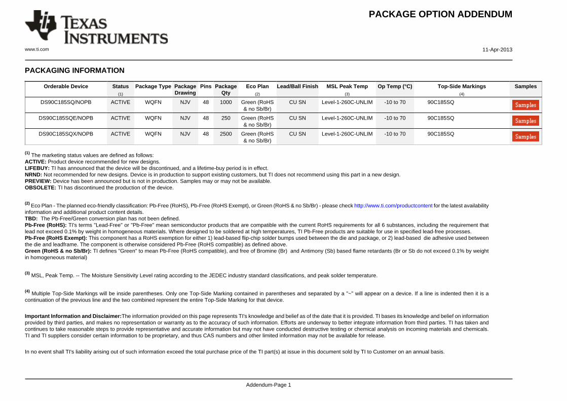
PACKAGING INFORMATION
Orderable Device Status(1)
Package Type PackageDrawing
Pins PackageQty
Eco Plan(2)
Lead/Ball Finish MSL Peak Temp(3)
Op Temp (°C) Top-Side Markings(4)
Samples
DS90C185SQ/NOPB ACTIVE WQFN NJV 48 1000 Green (RoHS& no Sb/Br)
CU SN Level-1-260C-UNLIM -10 to 70 90C185SQ
DS90C185SQE/NOPB ACTIVE WQFN NJV 48 250 Green (RoHS& no Sb/Br)
CU SN Level-1-260C-UNLIM -10 to 70 90C185SQ
DS90C185SQX/NOPB ACTIVE WQFN NJV 48 2500 Green (RoHS& no Sb/Br)
CU SN Level-1-260C-UNLIM -10 to 70 90C185SQ
(1) The marketing status values are defined as follows:ACTIVE: Product device recommended for new designs.LIFEBUY: TI has announced that the device will be discontinued, and a lifetime-buy period is in effect.NRND: Not recommended for new designs. Device is in production to support existing customers, but TI does not recommend using this part in a new design.PREVIEW: Device has been announced but is not in production. Samples may or may not be available.OBSOLETE: TI has discontinued the production of the device.
(2) Eco Plan - The planned eco-friendly classification: Pb-Free (RoHS), Pb-Free (RoHS Exempt), or Green (RoHS & no Sb/Br) - please check http://www.ti.com/productcontent for the latest availabilityinformation and additional product content details.TBD: The Pb-Free/Green conversion plan has not been defined.Pb-Free (RoHS): TI's terms "Lead-Free" or "Pb-Free" mean semiconductor products that are compatible with the current RoHS requirements for all 6 substances, including the requirement thatlead not exceed 0.1% by weight in homogeneous materials. Where designed to be soldered at high temperatures, TI Pb-Free products are suitable for use in specified lead-free processes.Pb-Free (RoHS Exempt): This component has a RoHS exemption for either 1) lead-based flip-chip solder bumps used between the die and package, or 2) lead-based die adhesive used betweenthe die and leadframe. The component is otherwise considered Pb-Free (RoHS compatible) as defined above.Green (RoHS & no Sb/Br): TI defines "Green" to mean Pb-Free (RoHS compatible), and free of Bromine (Br) and Antimony (Sb) based flame retardants (Br or Sb do not exceed 0.1% by weightin homogeneous material)
(3) MSL, Peak Temp. -- The Moisture Sensitivity Level rating according to the JEDEC industry standard classifications, and peak solder temperature.
(4) Multiple Top-Side Markings will be inside parentheses. Only one Top-Side Marking contained in parentheses and separated by a "~" will appear on a device. If a line is indented then it is acontinuation of the previous line and the two combined represent the entire Top-Side Marking for that device.
Important Information and Disclaimer:The information provided on this page represents TI's knowledge and belief as of the date that it is provided. TI bases its knowledge and belief on informationprovided by third parties, and makes no representation or warranty as to the accuracy of such information. Efforts are underway to better integrate information from third parties. TI has taken andcontinues to take reasonable steps to provide representative and accurate information but may not have conducted destructive testing or chemical analysis on incoming materials and chemicals.TI and TI suppliers consider certain information to be proprietary, and thus CAS numbers and other limited information may not be available for release.
In no event shall TI's liability arising out of such information exceed the total purchase price of the TI part(s) at issue in this document sold by TI to Customer on an annual basis.

TAPE AND REEL INFORMATION
*All dimensions are nominal
Device PackageType
PackageDrawing
Pins SPQ ReelDiameter
(mm)
ReelWidth
W1 (mm)
A0(mm)
B0(mm)
K0(mm)
P1(mm)
W(mm)
Pin1Quadrant
DS90C185SQ/NOPB WQFN NJV 48 1000 330.0 16.4 6.3 6.3 1.5 12.0 16.0 Q1
DS90C185SQE/NOPB WQFN NJV 48 250 178.0 16.4 6.3 6.3 1.5 12.0 16.0 Q1
DS90C185SQX/NOPB WQFN NJV 48 2500 330.0 16.4 6.3 6.3 1.5 12.0 16.0 Q1
PACKAGE MATERIALS INFORMATION
www.ti.com 11-Oct-2013
Pack Materials-Page 1

*All dimensions are nominal
Device Package Type Package Drawing Pins SPQ Length (mm) Width (mm) Height (mm)
DS90C185SQ/NOPB WQFN NJV 48 1000 367.0 367.0 35.0
DS90C185SQE/NOPB WQFN NJV 48 250 210.0 185.0 35.0
DS90C185SQX/NOPB WQFN NJV 48 2500 367.0 367.0 35.0
PACKAGE MATERIALS INFORMATION
www.ti.com 11-Oct-2013
Pack Materials-Page 2

MECHANICAL DATA
NJV0048A
www.ti.com
SQF48A (Rev A)

IMPORTANT NOTICE
Texas Instruments Incorporated and its subsidiaries (TI) reserve the right to make corrections, enhancements, improvements and otherchanges to its semiconductor products and services per JESD46, latest issue, and to discontinue any product or service per JESD48, latestissue. Buyers should obtain the latest relevant information before placing orders and should verify that such information is current andcomplete. All semiconductor products (also referred to herein as “components”) are sold subject to TI’s terms and conditions of salesupplied at the time of order acknowledgment.
TI warrants performance of its components to the specifications applicable at the time of sale, in accordance with the warranty in TI’s termsand conditions of sale of semiconductor products. Testing and other quality control techniques are used to the extent TI deems necessaryto support this warranty. Except where mandated by applicable law, testing of all parameters of each component is not necessarilyperformed.
TI assumes no liability for applications assistance or the design of Buyers’ products. Buyers are responsible for their products andapplications using TI components. To minimize the risks associated with Buyers’ products and applications, Buyers should provideadequate design and operating safeguards.
TI does not warrant or represent that any license, either express or implied, is granted under any patent right, copyright, mask work right, orother intellectual property right relating to any combination, machine, or process in which TI components or services are used. Informationpublished by TI regarding third-party products or services does not constitute a license to use such products or services or a warranty orendorsement thereof. Use of such information may require a license from a third party under the patents or other intellectual property of thethird party, or a license from TI under the patents or other intellectual property of TI.
Reproduction of significant portions of TI information in TI data books or data sheets is permissible only if reproduction is without alterationand is accompanied by all associated warranties, conditions, limitations, and notices. TI is not responsible or liable for such altereddocumentation. Information of third parties may be subject to additional restrictions.
Resale of TI components or services with statements different from or beyond the parameters stated by TI for that component or servicevoids all express and any implied warranties for the associated TI component or service and is an unfair and deceptive business practice.TI is not responsible or liable for any such statements.
Buyer acknowledges and agrees that it is solely responsible for compliance with all legal, regulatory and safety-related requirementsconcerning its products, and any use of TI components in its applications, notwithstanding any applications-related information or supportthat may be provided by TI. Buyer represents and agrees that it has all the necessary expertise to create and implement safeguards whichanticipate dangerous consequences of failures, monitor failures and their consequences, lessen the likelihood of failures that might causeharm and take appropriate remedial actions. Buyer will fully indemnify TI and its representatives against any damages arising out of the useof any TI components in safety-critical applications.
In some cases, TI components may be promoted specifically to facilitate safety-related applications. With such components, TI’s goal is tohelp enable customers to design and create their own end-product solutions that meet applicable functional safety standards andrequirements. Nonetheless, such components are subject to these terms.
No TI components are authorized for use in FDA Class III (or similar life-critical medical equipment) unless authorized officers of the partieshave executed a special agreement specifically governing such use.
Only those TI components which TI has specifically designated as military grade or “enhanced plastic” are designed and intended for use inmilitary/aerospace applications or environments. Buyer acknowledges and agrees that any military or aerospace use of TI componentswhich have not been so designated is solely at the Buyer's risk, and that Buyer is solely responsible for compliance with all legal andregulatory requirements in connection with such use.
TI has specifically designated certain components as meeting ISO/TS16949 requirements, mainly for automotive use. In any case of use ofnon-designated products, TI will not be responsible for any failure to meet ISO/TS16949.
Products Applications
Audio www.ti.com/audio Automotive and Transportation www.ti.com/automotive
Amplifiers amplifier.ti.com Communications and Telecom www.ti.com/communications
Data Converters dataconverter.ti.com Computers and Peripherals www.ti.com/computers
DLP® Products www.dlp.com Consumer Electronics www.ti.com/consumer-apps
DSP dsp.ti.com Energy and Lighting www.ti.com/energy
Clocks and Timers www.ti.com/clocks Industrial www.ti.com/industrial
Interface interface.ti.com Medical www.ti.com/medical
Logic logic.ti.com Security www.ti.com/security
Power Mgmt power.ti.com Space, Avionics and Defense www.ti.com/space-avionics-defense
Microcontrollers microcontroller.ti.com Video and Imaging www.ti.com/video
RFID www.ti-rfid.com
OMAP Applications Processors www.ti.com/omap TI E2E Community e2e.ti.com
Wireless Connectivity www.ti.com/wirelessconnectivity
Mailing Address: Texas Instruments, Post Office Box 655303, Dallas, Texas 75265Copyright © 2013, Texas Instruments Incorporated