Embed Size (px)
Citation preview
Sequential Circuits:
Latches & Flip-Flops
Fall 2019 Fundamentals of Digital Systems Design by Todor Stefanov, Leiden University
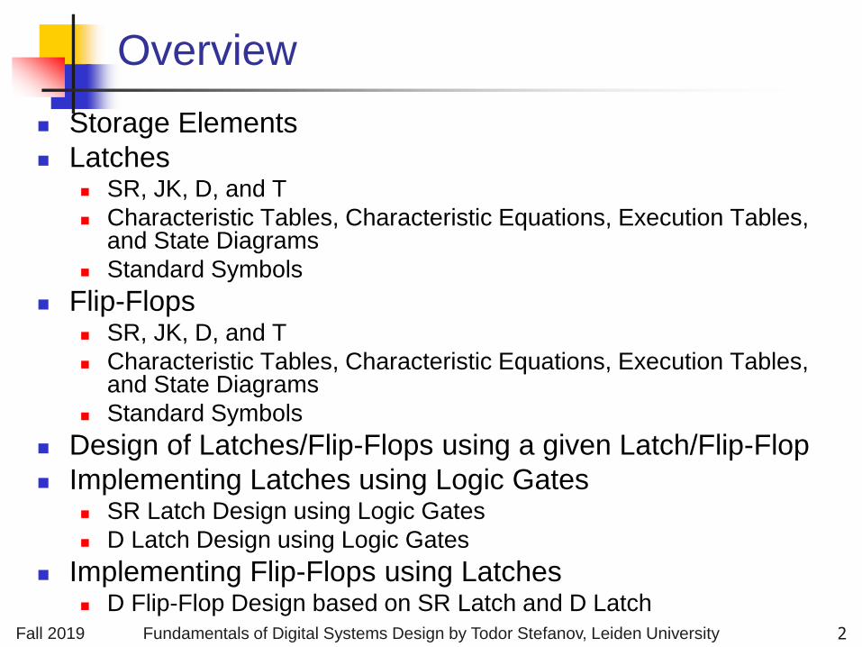
Overview
Storage Elements
Latches SR, JK, D, and T
Characteristic Tables, Characteristic Equations, Execution Tables, and State Diagrams
Standard Symbols
Flip-Flops SR, JK, D, and T
Characteristic Tables, Characteristic Equations, Execution Tables, and State Diagrams
Standard Symbols
Design of Latches/Flip-Flops using a given Latch/Flip-Flop
Implementing Latches using Logic Gates SR Latch Design using Logic Gates
D Latch Design using Logic Gates
Implementing Flip-Flops using Latches D Flip-Flop Design based on SR Latch and D Latch
2
Fall 2019 Fundamentals of Digital Systems Design by Todor Stefanov, Leiden University
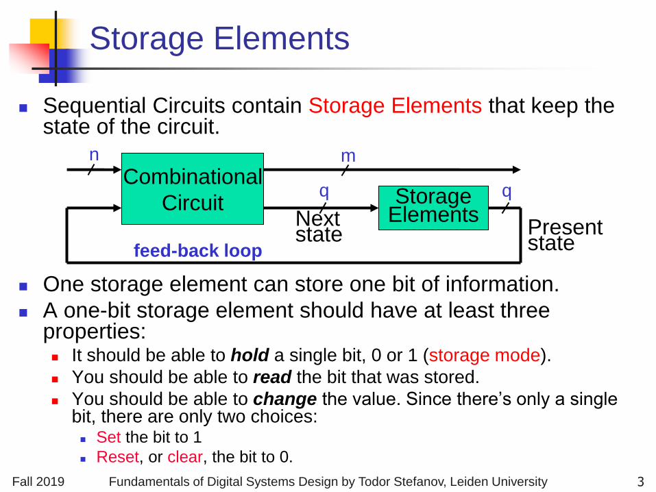
Storage Elements
Sequential Circuits contain Storage Elements that keep the state of the circuit.
One storage element can store one bit of information.
A one-bit storage element should have at least three properties: It should be able to hold a single bit, 0 or 1 (storage mode).
You should be able to read the bit that was stored.
You should be able to change the value. Since there’s only a single bit, there are only two choices: Set the bit to 1
Reset, or clear, the bit to 0.
n m
Combinational
Circuit Storage Elements Next
state Present state
q
feed-back loop
q
3
Fall 2019 Fundamentals of Digital Systems Design by Todor Stefanov, Leiden University
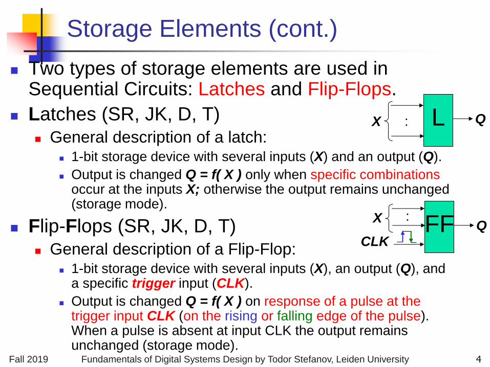
Storage Elements (cont.)
Two types of storage elements are used in Sequential Circuits: Latches and Flip-Flops.
Latches (SR, JK, D, T) General description of a latch:
1-bit storage device with several inputs (X) and an output (Q).
Output is changed Q = f( X ) only when specific combinations occur at the inputs X; otherwise the output remains unchanged (storage mode).
Flip-Flops (SR, JK, D, T) General description of a Flip-Flop:
1-bit storage device with several inputs (X), an output (Q), and a specific trigger input (CLK).
Output is changed Q = f( X ) on response of a pulse at the trigger input CLK (on the rising or falling edge of the pulse). When a pulse is absent at input CLK the output remains unchanged (storage mode).
L : X Q
FF : X
Q CLK
4
Fall 2019 Fundamentals of Digital Systems Design by Todor Stefanov, Leiden University
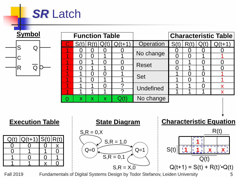
SR Latch
1
S
R
C
Q
Q
x x 1 1 0 0 1 0
Q(t+1)
1 1 1 1 0 0 0 0
S(t)
1 1 0 1 1 0 0 0
1 0 0 1
1
0
R(t)
1
0
Q(t)
0 1 0 x
R(t)
1 1 0 0
Q(t)
x 1 0 0 1 1 0 0
Q(t+1) S(t)
State Diagram
Q=0 Q=1
S,R = 0,X
S,R = 1,0
S,R = 0,1
S,R = X,0
Symbol Function Table
Execution Table
Characteristic Table
Characteristic Equation
1 S(t)
Q(t)
R(t)
x
1
Q(t+1) = S(t) + R(t)’•Q(t)
x
? ? 1 1 0 0 1 0
Q(t+1)
1 1 1 1 0 0 0 0
S(t)
1 1 0 1 1 0 0 0
1 0 0 1
1
0
R(t)
1
0
Q(t) C
Q(t) x x x
Operation
No change
Reset
Set
Undefined
No change
1 1 1 1 1 1 1 1
0
5
Fall 2019 Fundamentals of Digital Systems Design by Todor Stefanov, Leiden University
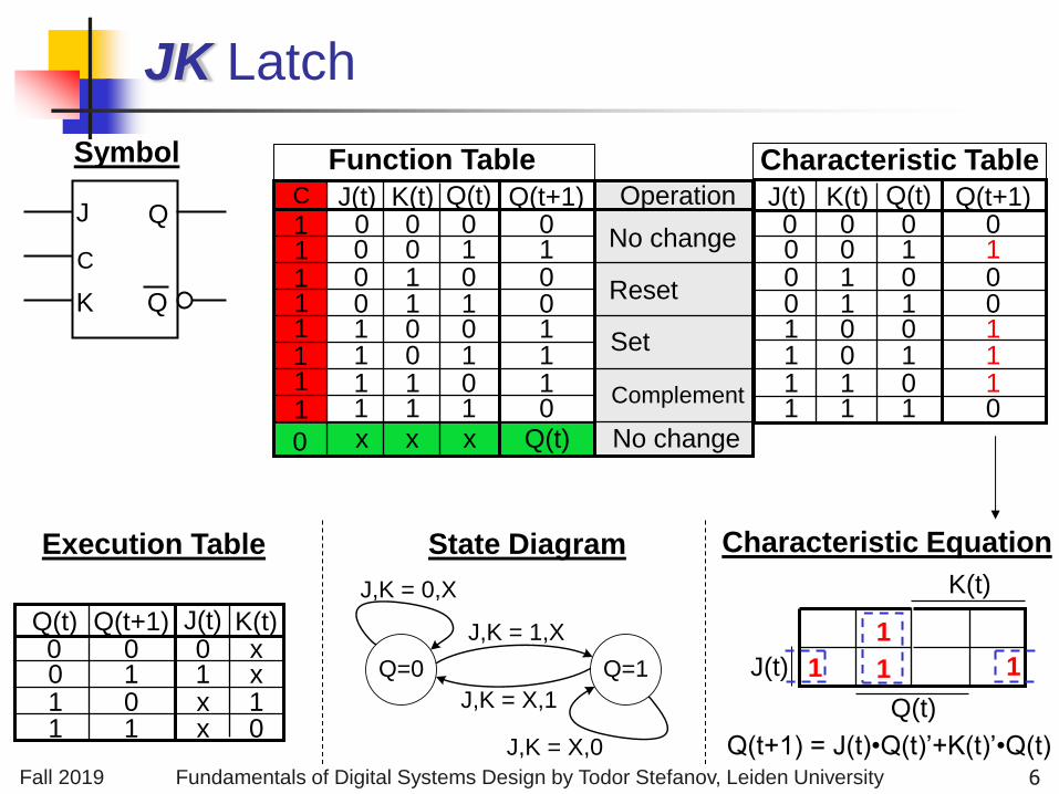
JK Latch
J
K
C
Q
Q
0 1 1 1 0 0 1 0
Q(t+1)
1 1 1 1 0 0 0 0
J(t)
1 1 0 1 1 0 0 0
1 0 0 1
1
0
K(t)
1
0
Q(t)
0 1 x x
K(t)
1 1 0 0
Q(t)
x 1 x 0 1 1 0 0
Q(t+1) J(t)
State Diagram
Q=0 Q=1
J,K = 0,X
J,K = 1,X
J,K = X,1
J,K = X,0
Symbol Function Table
Execution Table
Characteristic Table
Characteristic Equation
1 J(t)
Q(t)
K(t)
1 1
1
Q(t+1) = J(t)•Q(t)’+K(t)’•Q(t)
0 1 1 1 0 0 1 0
Q(t+1)
1 1 1 1 0 0 0 0
J(t)
1 1 0 1 1 0 0 0
1 0 0 1
1
0
K(t)
1
0
Q(t) C
Q(t) x x x
Operation
No change
Reset
Set
Complement
No change
1 1 1 1 1 1 1 1
0
6
Fall 2019 Fundamentals of Digital Systems Design by Todor Stefanov, Leiden University
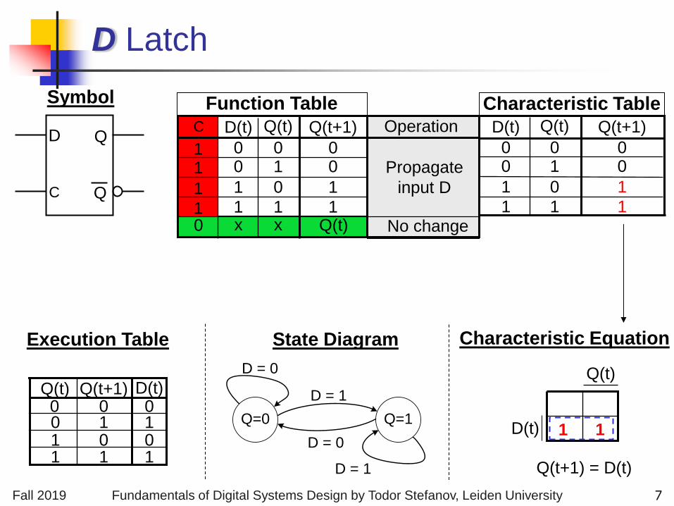
D Latch
1 1 0 0
Q(t)
1 1 0 0 1 1 0 0
Q(t+1) D(t)
State Diagram
Q=0 Q=1
D = 0
D = 1
D = 0
D = 1
D
C
Q
Q
Symbol Function Table
Execution Table
Characteristic Table
Characteristic Equation
1 D(t)
Q(t)
1
Q(t+1) = D(t)
1
1
0 0
Q(t+1)
1 1
0 1
1 0 0 0
D(t) Q(t)
Propagate
input D
No change 1
1
0 0
Q(t+1)
1 1
0 1
1 0 0 0
x
D(t)
x
Q(t) C
Q(t)
Operation
1
1
1 1
0
7

Fall 2019 Fundamentals of Digital Systems Design by Todor Stefanov, Leiden University
T Latch
1 1 0 0
Q(t)
0 1 1 0 1 1 0 0
Q(t+1) T(t)
State Diagram
Q=0 Q=1
T = 0
T = 1
T = 1
T = 0
T
C
Q
Q
Symbol Function Table
Execution Table
Characteristic Table
Characteristic Equation
1 T(t)
Q(t)
1
Q(t+1) = T(t) Q(t)
0
1
1 0
Q(t+1)
1 1
0 1
1 0 0 0
T(t) Q(t)
Complement
No change 0
1
1 0
Q(t+1)
1 1
0 1
1 0 0 0
x
T(t)
x
Q(t) C
Q(t)
Operation
No change
1
1
1 1
0
8
Fall 2019 Fundamentals of Digital Systems Design by Todor Stefanov, Leiden University
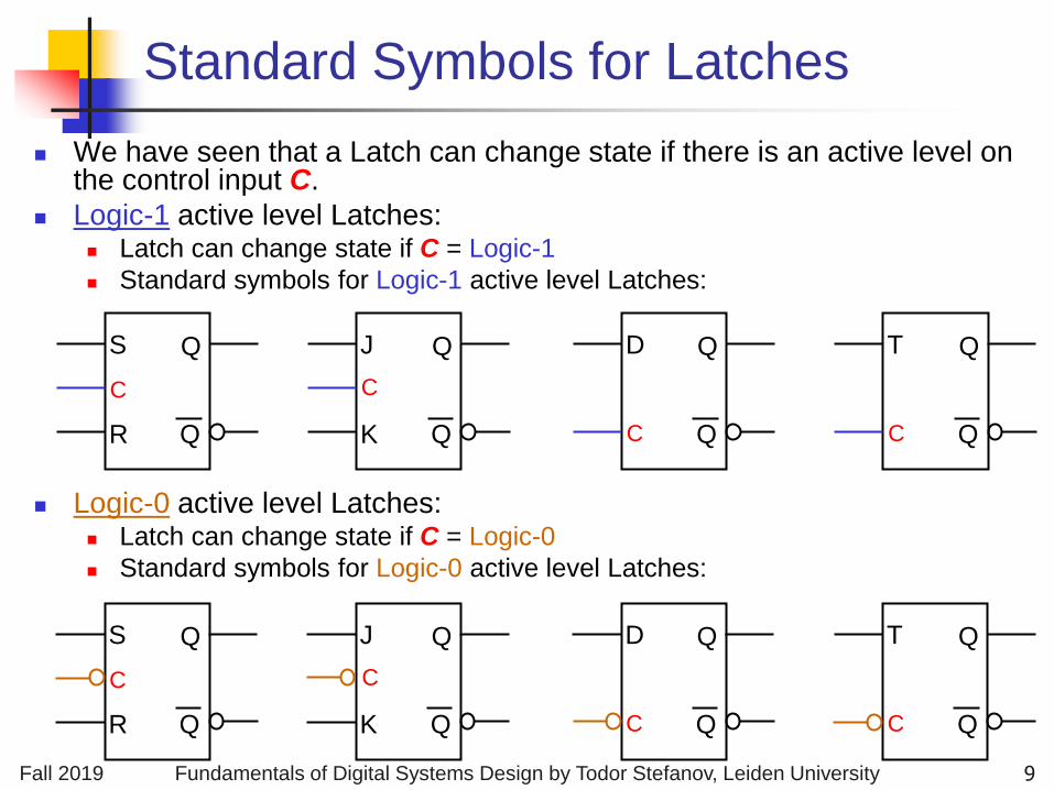
We have seen that a Latch can change state if there is an active level on the control input C.
Logic-1 active level Latches: Latch can change state if C = Logic-1
Standard symbols for Logic-1 active level Latches:
Logic-0 active level Latches: Latch can change state if C = Logic-0
Standard symbols for Logic-0 active level Latches:
Standard Symbols for Latches
S
R
C
Q
Q
J
K
C
Q
Q
D
C
Q
Q
T
C
Q
Q
S
R
C
Q
Q
J
K
C
Q
Q
D
C
Q
Q
T
C
Q
Q
9

Fall 2019 Fundamentals of Digital Systems Design by Todor Stefanov, Leiden University
1
SR Flip-Flop
S
R
CLK
Q
Q
x x 1 1 0 0 1 0
Q(t+1)
1 1 1 1 0 0 0 0
S(t)
1 1 0 1 1 0 0 0
1 0 0 1
1
0
R(t)
1
0
Q(t)
0 1 0 x
R(t)
1 1 0 0
Q(t)
x 1 0 0 1 1 0 0
Q(t+1) S(t)
State Diagram
Q=0 Q=1
S,R = 0,X
S,R = 1,0
S,R = 0,1
S,R = X,0
Symbol
? ? 1 1 0 0 1 0
Q(t+1)
1 1 1 1 0 0 0 0
S(t)
1 1 0 1 1 0 0 0
1 0 0 1
1
0
R(t)
1
0
Q(t) CLK
Q(t) x x x
Operation
No change
Reset
Set
Undefined
No change
Function Table
- rising edge
- 1 or 0 or
falling edge
Execution Table
Characteristic Table
Characteristic Equation
1 S(t)
Q(t)
R(t)
x
1
Q(t+1) = S(t) + R(t)’•Q(t)
x
10
Fall 2019 Fundamentals of Digital Systems Design by Todor Stefanov, Leiden University
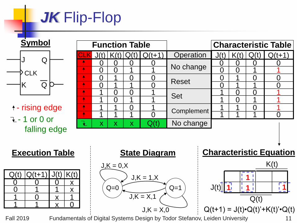
JK Flip-Flop
J
K
CLK
Q
Q
0 1 1 1 0 0 1 0
Q(t+1)
1 1 1 1 0 0 0 0
J(t)
1 1 0 1 1 0 0 0
1 0 0 1
1
0
K(t)
1
0
Q(t)
0 1 x x
K(t)
1 1 0 0
Q(t)
x 1 x 0 1 1 0 0
Q(t+1) J(t)
State Diagram
Q=0 Q=1
J,K = 0,X
J,K = 1,X
J,K = X,1
J,K = X,0
Symbol
0 1 1 1 0 0 1 0
Q(t+1)
1 1 1 1 0 0 0 0
J(t)
1 1 0 1 1 0 0 0
1 0 0 1
1
0
K(t)
1
0
Q(t) CLK
Q(t) x x x
Operation
No change
Reset
Set
Complement
No change
Function Table
- rising edge
- 1 or 0 or
falling edge
Execution Table
Characteristic Table
Characteristic Equation
1 J(t)
Q(t)
K(t)
1 1
1
Q(t+1) = J(t)•Q(t)’+K(t)’•Q(t) 11
Fall 2019 Fundamentals of Digital Systems Design by Todor Stefanov, Leiden University
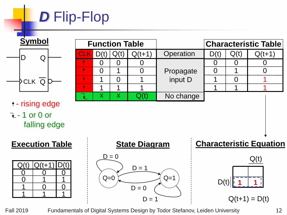
D Flip-Flop
1 1 0 0
Q(t)
1 1 0 0 1 1 0 0
Q(t+1) D(t)
State Diagram
Q=0 Q=1
D = 0
D = 1
D = 0
D = 1
D
CLK
Q
Q
Symbol
Propagate
input D
No change 1
1
0 0
Q(t+1)
1 1
0 1
1 0 0 0
x
D(t)
x
Q(t) CLK
Q(t)
Operation
Function Table
- rising edge
- 1 or 0 or
falling edge
Execution Table
Characteristic Table
Characteristic Equation
1 D(t)
Q(t)
1
Q(t+1) = D(t)
1
1
0 0
Q(t+1)
1 1
0 1
1 0 0 0
D(t) Q(t)
12
Fall 2019 Fundamentals of Digital Systems Design by Todor Stefanov, Leiden University
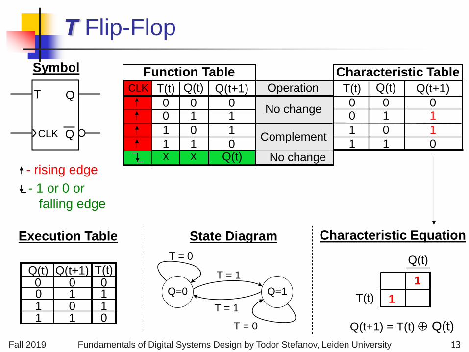
T Flip-Flop
1 1 0 0
Q(t)
0 1 1 0 1 1 0 0
Q(t+1) T(t)
State Diagram
Q=0 Q=1
T = 0
T = 1
T = 1
T = 0
T
CLK
Q
Q
Symbol
Complement
No change 0
1
1 0
Q(t+1)
1 1
0 1
1 0 0 0
x
T(t)
x
Q(t) CLK
Q(t)
Operation
Function Table
- rising edge
- 1 or 0 or
falling edge
Execution Table
Characteristic Table
Characteristic Equation
1 T(t)
Q(t)
1
Q(t+1) = T(t) Q(t)
0
1
1 0
Q(t+1)
1 1
0 1
1 0 0 0
T(t) Q(t)
No change
13
Fall 2019 Fundamentals of Digital Systems Design by Todor Stefanov, Leiden University
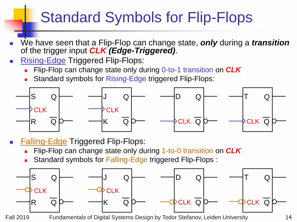
We have seen that a Flip-Flop can change state, only during a transition of the trigger input CLK (Edge-Triggered).
Rising-Edge Triggered Flip-Flops: Flip-Flop can change state only during 0-to-1 transition on CLK
Standard symbols for Rising-Edge triggered Flip-Flops:
Falling-Edge Triggered Flip-Flops: Flip-Flop can change state only during 1-to-0 transition on CLK
Standard symbols for Falling-Edge triggered Flip-Flops :
Standard Symbols for Flip-Flops
S
R
CLK
Q
Q
J
K
CLK
Q
Q
D
CLK
Q
Q
T
CLK
Q
Q
S
R
CLK
Q
Q
J
K
CLK
Q
Q
D
CLK
Q
Q
T
CLK
Q
Q
14
Fall 2019 Fundamentals of Digital Systems Design by Todor Stefanov, Leiden University
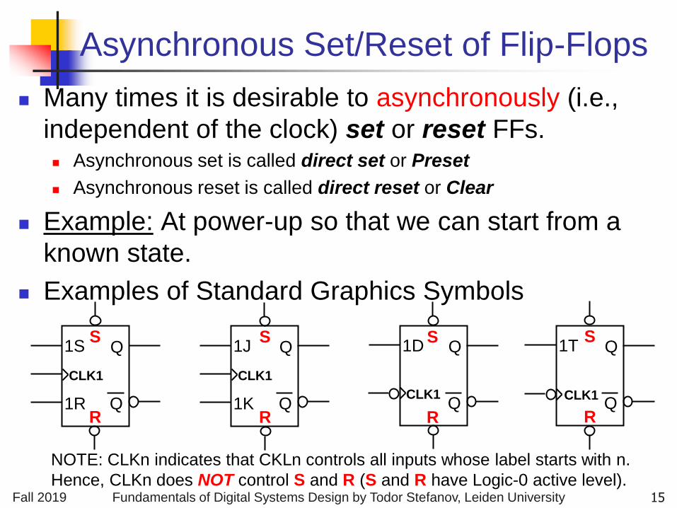
Asynchronous Set/Reset of Flip-Flops
Many times it is desirable to asynchronously (i.e.,
independent of the clock) set or reset FFs. Asynchronous set is called direct set or Preset
Asynchronous reset is called direct reset or Clear
Example: At power-up so that we can start from a
known state.
Examples of Standard Graphics Symbols
1S
1R
CLK1
Q
Q
1J
1K
CLK1
Q
Q
1D
CLK1
Q
Q
1T
CLK1
Q
Q
S
R
S
R
S
R
S
R
NOTE: CLKn indicates that CKLn controls all inputs whose label starts with n.
Hence, CLKn does NOT control S and R (S and R have Logic-0 active level). 15
Fall 2019 Fundamentals of Digital Systems Design by Todor Stefanov, Leiden University
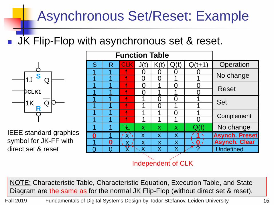
Asynchronous Set/Reset: Example
JK Flip-Flop with asynchronous set & reset.
1J
1K
CLK1
Q
Q
S
R
IEEE standard graphics
symbol for JK-FF with
direct set & reset
Function Table
0 1 1 1 0 0 1 0
Q(t+1)
1 1 1 1 0 0 0 0
J(t)
1 1 0 1 1 0 0 0
1 0 0 1
1
0
K(t)
1
0
Q(t) CLK
Q(t) x x x
Operation
No change
Reset
Set
Complement
No change
1 R S
? 0 1 x
1 1 1 1 1 1 1 1 1 1 1 1 1 1 1 1 1
1 0 0 1 0 0
x x x x x x x x x x x
Asynch. Preset Asynch. Clear
Undefined
NOTE: Characteristic Table, Characteristic Equation, Execution Table, and State
Diagram are the same as for the normal JK Flip-Flop (without direct set & reset).
Independent of CLK
16
Fall 2019 Fundamentals of Digital Systems Design by Todor Stefanov, Leiden University
Latches & Flip-Flops
The Latches are Level-triggered whereas the Flip-
Flops are Edge-triggered.
SR Latch and SR Flip-Flop have the same
Characteristic Table, Characteristic Equation,
Execution Table, and State Diagram.
The above is valid for the other pairs: JK Latch –
JK Flip-Flop, D Latch – D Flip-Flop, T Latch – T
Flip-Flop.
Given a Latch of type X (X is SR or JK or D or T),
any other type of Latch can be designed using X.
Given a Flip-Flop of type X (X is SR or JK or D or T),
any other type of Flip-Flop can be designed using X. 17
Fall 2019 Fundamentals of Digital Systems Design by Todor Stefanov, Leiden University
Design Procedure
The procedure to design Latches with a given Latch of type X is the same as the procedure to design Flip-Flops with a given Flip-Flop of type X.
So, I will illustrate the design procedure for Flip-Flops.
Given D Flip-Flop, design: SR Flip-Flop, JK Flip-Flop, and T Flip-Flop (see this lecture)
Given SR Flip-Flop, design: D Flip-Flop (see this lecture)
JK Flip-Flop, and T Flip-Flop (see homework 7)
Given JK Flip-Flop, design: SR Flip-Flop, D Flip-Flop (see homework 7)
T Flip-Flop (try at home)
Given T Flip-Flop, design: SR Flip-Flop, JK Flip-Flop, and D Flip-Flop (try at home)
18
Fall 2019 Fundamentals of Digital Systems Design by Todor Stefanov, Leiden University
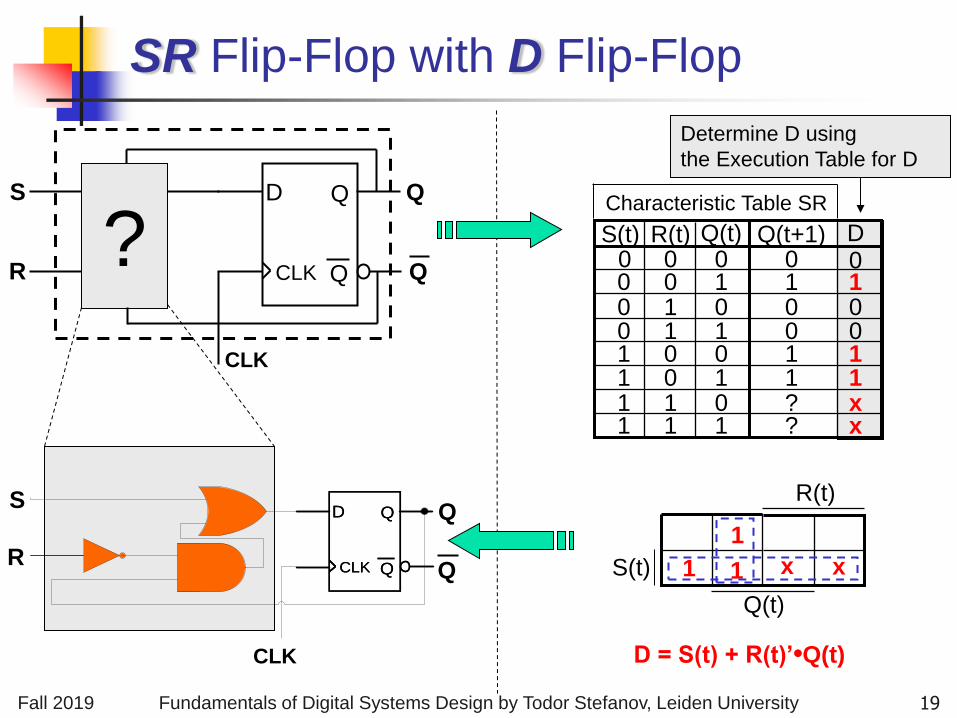
SR Flip-Flop with D Flip-Flop
D
CLK
Q
Q ?
S
R
CLK
Q
Q
x x 1 1 0 0 1 0 D
? ? 1 1 0 0 1 0
Q(t+1)
1 1 1 1 0 0 0 0
S(t)
1 1 0 1 1 0 0 0
1 0 0 1
1
0
R(t)
1
0
Q(t)
1 x S(t)
Q(t)
R(t)
1
1
D = S(t) + R(t)’•Q(t)
D
CLK
Q
Q
D
CLK
Q
Q
S
R
CLK
Q
Q
Characteristic Table SR
Determine D using
the Execution Table for D
x
19
Fall 2019 Fundamentals of Digital Systems Design by Todor Stefanov, Leiden University
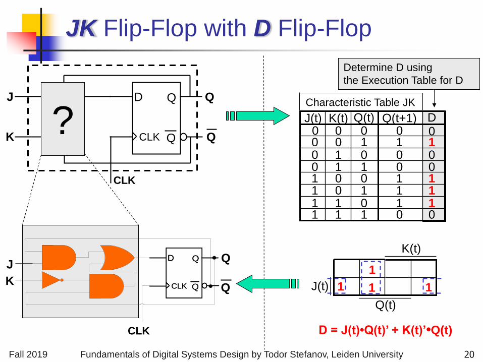
JK Flip-Flop with D Flip-Flop
D
CLK
Q
Q ?
J
K
CLK
Q
Q
0 1 1 1 0 0 1 0 D
0 1 1 1 0 0 1 0
Q(t+1)
1 1 1 1 0 0 0 0
J(t)
1 1 0 1 1 0 0 0
1 0 0 1
1
0
K(t)
1
0
Q(t)
1 1 J(t)
Q(t)
K(t)
1
1
D = J(t)•Q(t)’ + K(t)’•Q(t)
D
CLK
Q
Q
D
CLK
Q
Q
J
K
CLK
Q
Q
Characteristic Table JK
Determine D using
the Execution Table for D
20
Fall 2019 Fundamentals of Digital Systems Design by Todor Stefanov, Leiden University
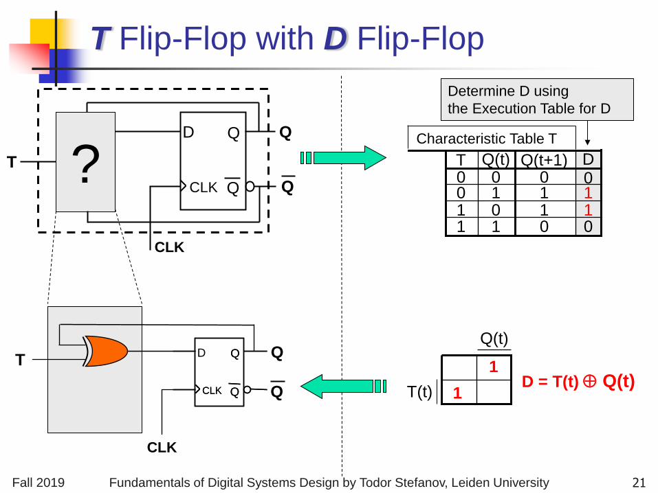
T Flip-Flop with D Flip-Flop
? T
CLK
Q
Q
0 1 1 0 D
0 1 1 0
Q(t+1)
1 1 0 1 1 0 0 0
T Q(t)
T
CLK
Q
Q
Characteristic Table T
Determine D using
the Execution Table for D
1 T(t)
Q(t)
1 D = T(t) Q(t)
D
CLK
Q
Q
D
CLK
Q
Q CLK
Q
Q
21
Fall 2019 Fundamentals of Digital Systems Design by Todor Stefanov, Leiden University
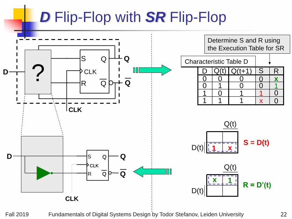
D Flip-Flop with SR Flip-Flop
S
R
CLK
Q
Q ? D
CLK
Q
Q
0 0 1 x R
x 1 0 0 S
1 1 0 0
Q(t+1)
1 1 0 1 1 0 0 0
D Q(t)
S = D(t)
R = D’(t)
D
CLK
Q
Q
Characteristic Table D
Determine S and R using
the Execution Table for SR
1 D(t)
Q(t)
x
D(t)
Q(t)
1 x
S
R
CLK
Q
Q
CLK
Q
Q
22
Fall 2019 Fundamentals of Digital Systems Design by Todor Stefanov, Leiden University
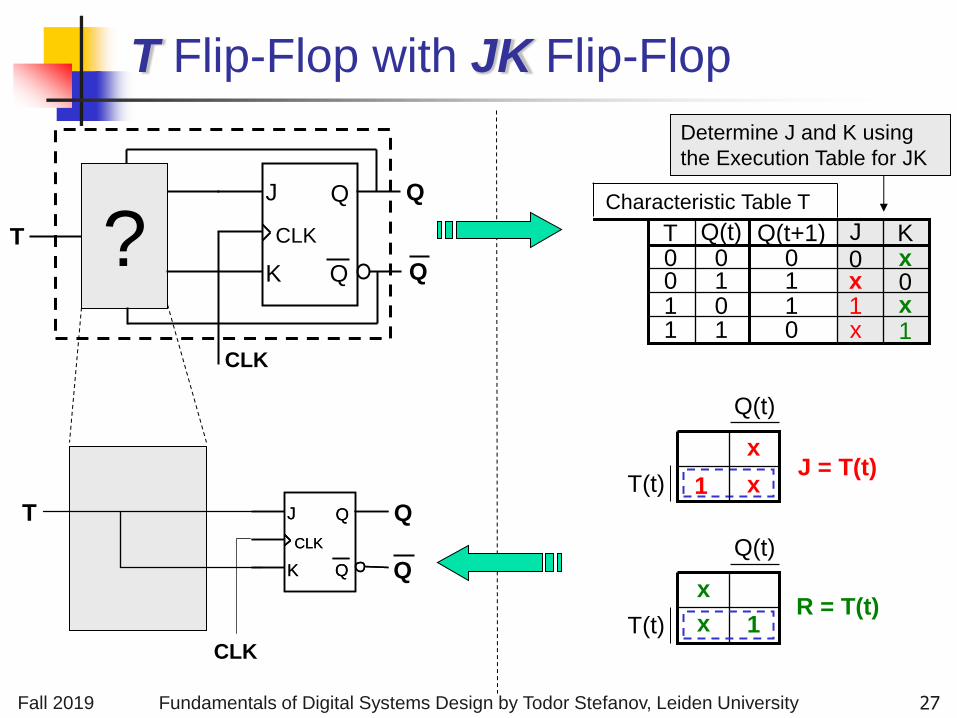
T Flip-Flop with JK Flip-Flop
J
K
CLK
Q
Q ? T
CLK
Q
Q
1 x 0 x K
x 1 x 0 J
0 1 1 0
Q(t+1)
1 1 0 1 1 0 0 0
T Q(t)
J = T(t)
T
CLK
Q
Q
Characteristic Table T
Determine J and K using
the Execution Table for JK
1 T(t)
Q(t)
x
x
J
K
CLK
Q
Q
J
K
CLK
Q
Q
R = T(t) T(t)
Q(t)
1
x
x
27
Fall 2019 Fundamentals of Digital Systems Design by Todor Stefanov, Leiden University
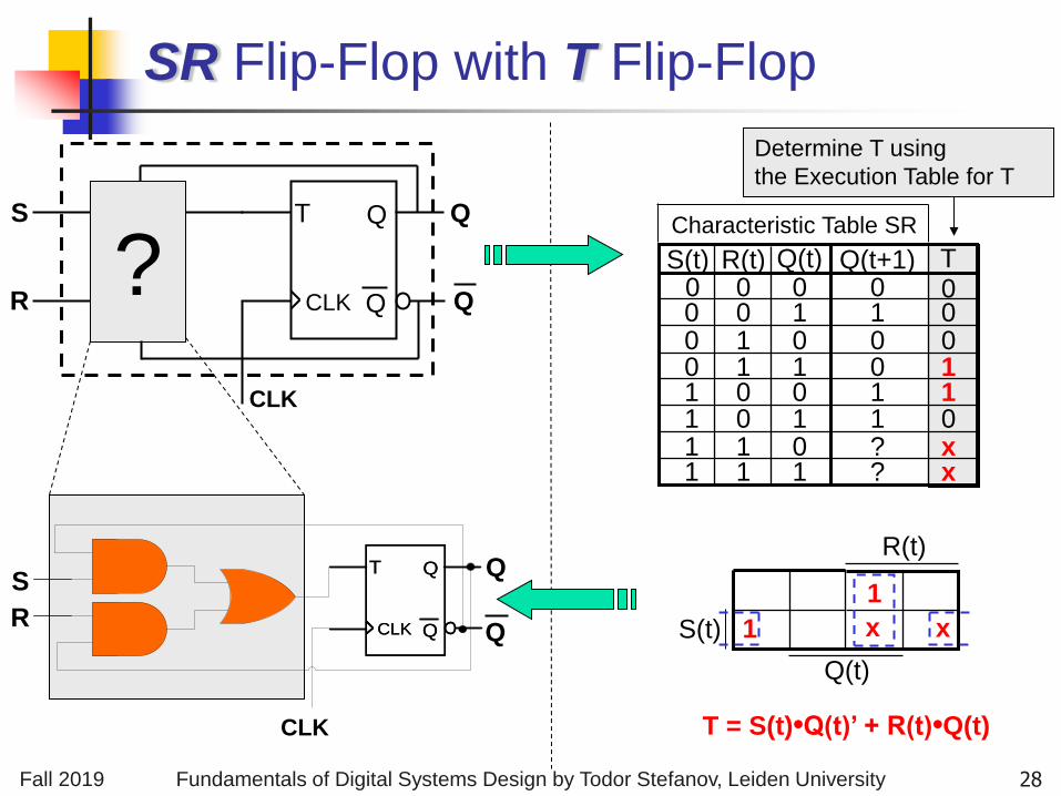
SR Flip-Flop with T Flip-Flop
T
CLK
Q
Q ?
S
R
CLK
Q
Q
x x 0 1 1 0 0 0 T
? ? 1 1 0 0 1 0
Q(t+1)
1 1 1 1 0 0 0 0
S(t)
1 1 0 1 1 0 0 0
1 0 0 1
1
0
R(t)
1
0
Q(t)
1 x S(t)
Q(t)
R(t)
1
T = S(t)•Q(t)’ + R(t)•Q(t)
Characteristic Table SR
Determine T using
the Execution Table for T
x
CLK
Q
Q
T
CLK
Q
Q
T
CLK
Q
Q
S
R
28
Fall 2019 Fundamentals of Digital Systems Design by Todor Stefanov, Leiden University
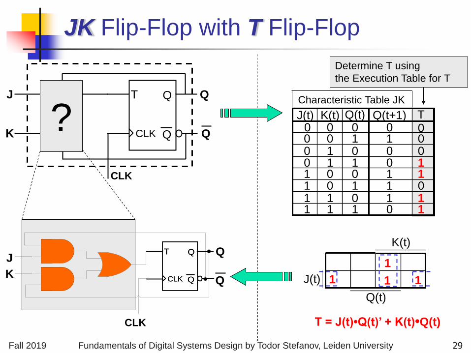
JK Flip-Flop with T Flip-Flop
T
CLK
Q
Q ?
J
K
CLK
Q
Q
1 1 0 1 1 0 0 0 T
0 1 1 1 0 0 1 0
Q(t+1)
1 1 1 1 0 0 0 0
J(t)
1 1 0 1 1 0 0 0
1 0 0 1
1
0
K(t)
1
0
Q(t)
1 1 J(t)
Q(t)
K(t)
1
1
T = J(t)•Q(t)’ + K(t)•Q(t)
T
CLK
Q
Q
T
CLK
Q
Q
J
K
CLK
Q
Q
Characteristic Table JK
Determine T using
the Execution Table for T
29
Fall 2019 Fundamentals of Digital Systems Design by Todor Stefanov, Leiden University
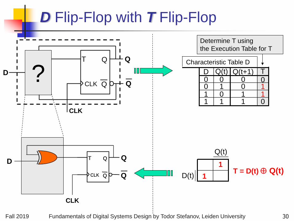
D Flip-Flop with T Flip-Flop
? D
CLK
Q
Q
0 1 1 0 T
1 1 0 0
Q(t+1)
1 1 0 1 1 0 0 0
D Q(t)
D
CLK
Q
Q
Characteristic Table D
Determine T using
the Execution Table for T
1 D(t)
Q(t)
1 T = D(t) Q(t)
T
CLK
Q
Q
T
CLK
Q
Q
T
CLK
Q
Q
30
Fall 2019 Fundamentals of Digital Systems Design by Todor Stefanov, Leiden University
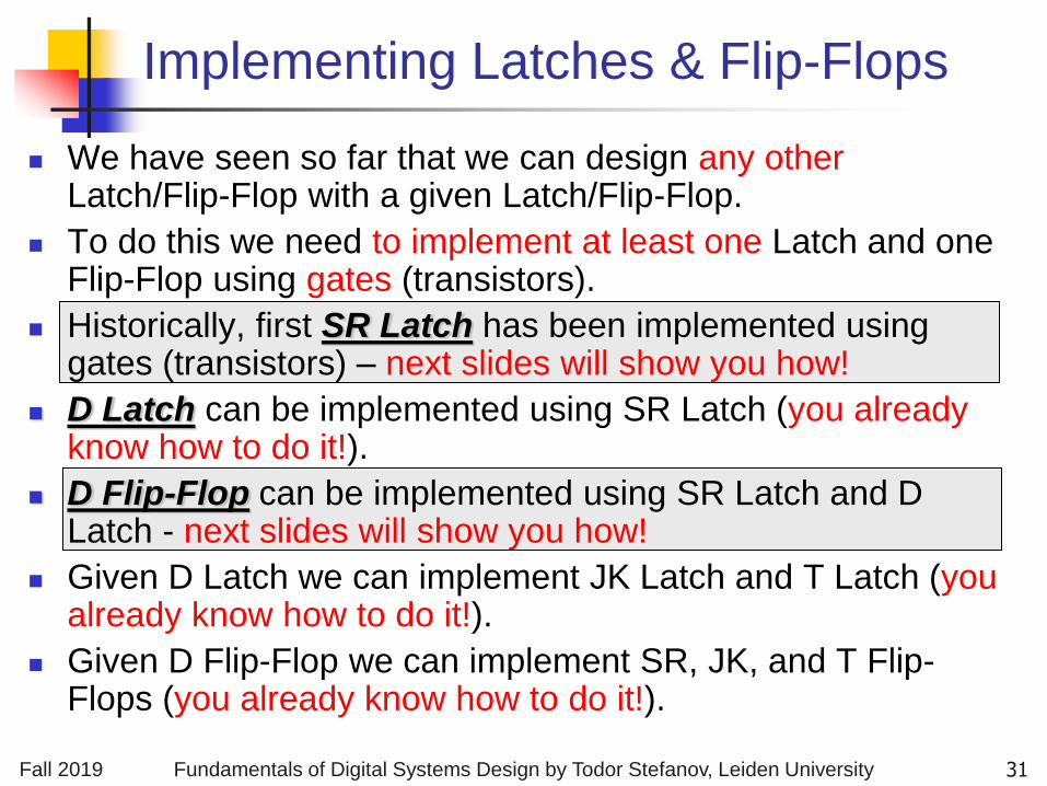
Implementing Latches & Flip-Flops
We have seen so far that we can design any other Latch/Flip-Flop with a given Latch/Flip-Flop.
To do this we need to implement at least one Latch and one Flip-Flop using gates (transistors).
Historically, first SR Latch has been implemented using gates (transistors) – next slides will show you how!
D Latch can be implemented using SR Latch (you already know how to do it!).
D Flip-Flop can be implemented using SR Latch and D Latch - next slides will show you how!
Given D Latch we can implement JK Latch and T Latch (you already know how to do it!).
Given D Flip-Flop we can implement SR, JK, and T Flip-Flops (you already know how to do it!).
31
Fall 2019 Fundamentals of Digital Systems Design by Todor Stefanov, Leiden University
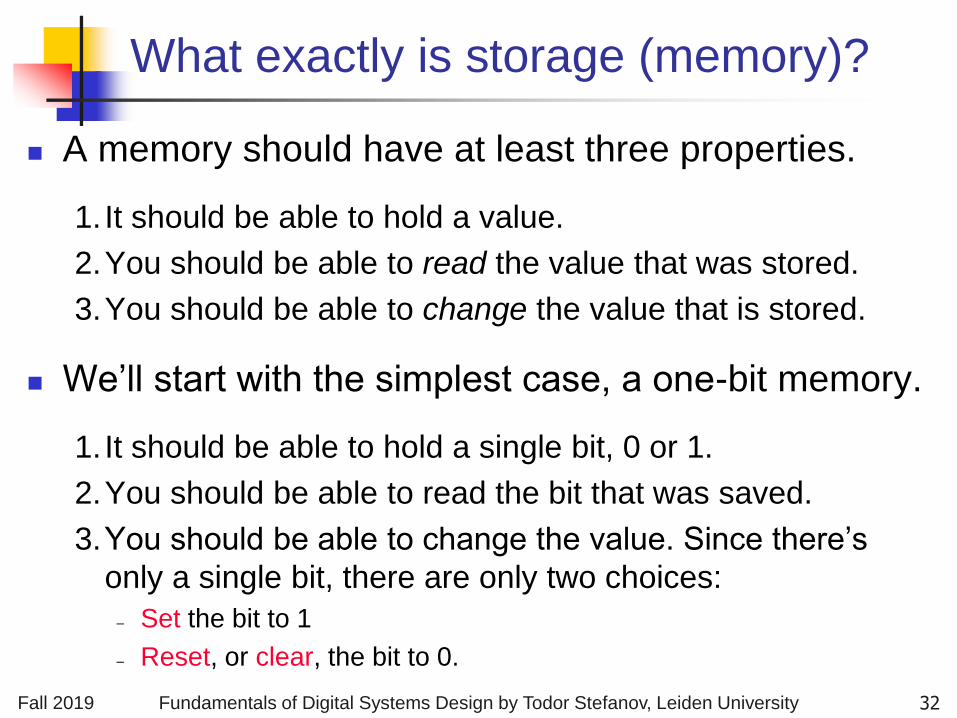
What exactly is storage (memory)?
A memory should have at least three properties.
1. It should be able to hold a value.
2. You should be able to read the value that was stored.
3. You should be able to change the value that is stored.
We’ll start with the simplest case, a one-bit memory.
1. It should be able to hold a single bit, 0 or 1.
2. You should be able to read the bit that was saved.
3. You should be able to change the value. Since there’s
only a single bit, there are only two choices:
– Set the bit to 1
– Reset, or clear, the bit to 0.
32
Fall 2019 Fundamentals of Digital Systems Design by Todor Stefanov, Leiden University
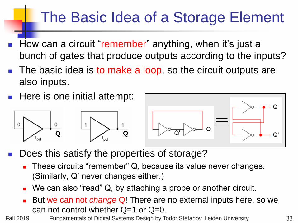
The Basic Idea of a Storage Element
How can a circuit “remember” anything, when it’s just a
bunch of gates that produce outputs according to the inputs?
The basic idea is to make a loop, so the circuit outputs are
also inputs.
Here is one initial attempt:
Does this satisfy the properties of storage?
These circuits “remember” Q, because its value never changes.
(Similarly, Q’ never changes either.)
We can also “read” Q, by attaching a probe or another circuit.
But we can not change Q! There are no external inputs here, so we
can not control whether Q=1 or Q=0.
Q Q
33
Fall 2019 Fundamentals of Digital Systems Design by Todor Stefanov, Leiden University
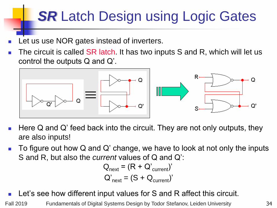
SR Latch Design using Logic Gates
Let us use NOR gates instead of inverters.
The circuit is called SR latch. It has two inputs S and R, which will let us
control the outputs Q and Q’.
Here Q and Q’ feed back into the circuit. They are not only outputs, they
are also inputs!
To figure out how Q and Q’ change, we have to look at not only the inputs
S and R, but also the current values of Q and Q’:
Qnext = (R + Q’current)’
Q’next = (S + Qcurrent)’
Let’s see how different input values for S and R affect this circuit.
34
Fall 2019 Fundamentals of Digital Systems Design by Todor Stefanov, Leiden University
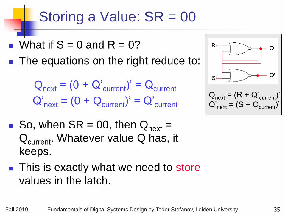
Storing a Value: SR = 00
What if S = 0 and R = 0?
The equations on the right reduce to:
Qnext = (0 + Q’current)’ = Qcurrent
Q’next = (0 + Qcurrent)’ = Q’current
So, when SR = 00, then Qnext =
Qcurrent. Whatever value Q has, it
keeps.
This is exactly what we need to store
values in the latch.
Qnext = (R + Q’current)’
Q’next = (S + Qcurrent)’
35
Fall 2019 Fundamentals of Digital Systems Design by Todor Stefanov, Leiden University
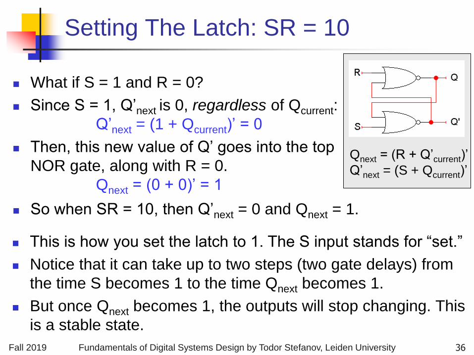
Setting The Latch: SR = 10
What if S = 1 and R = 0?
Since S = 1, Q’next is 0, regardless of Qcurrent:
Q’next = (1 + Qcurrent)’ = 0
Then, this new value of Q’ goes into the top
NOR gate, along with R = 0.
Qnext = (0 + 0)’ = 1
So when SR = 10, then Q’next = 0 and Qnext = 1.
Qnext = (R + Q’current)’
Q’next = (S + Qcurrent)’
This is how you set the latch to 1. The S input stands for “set.”
Notice that it can take up to two steps (two gate delays) from
the time S becomes 1 to the time Qnext becomes 1.
But once Qnext becomes 1, the outputs will stop changing. This
is a stable state.
36
Fall 2019 Fundamentals of Digital Systems Design by Todor Stefanov, Leiden University
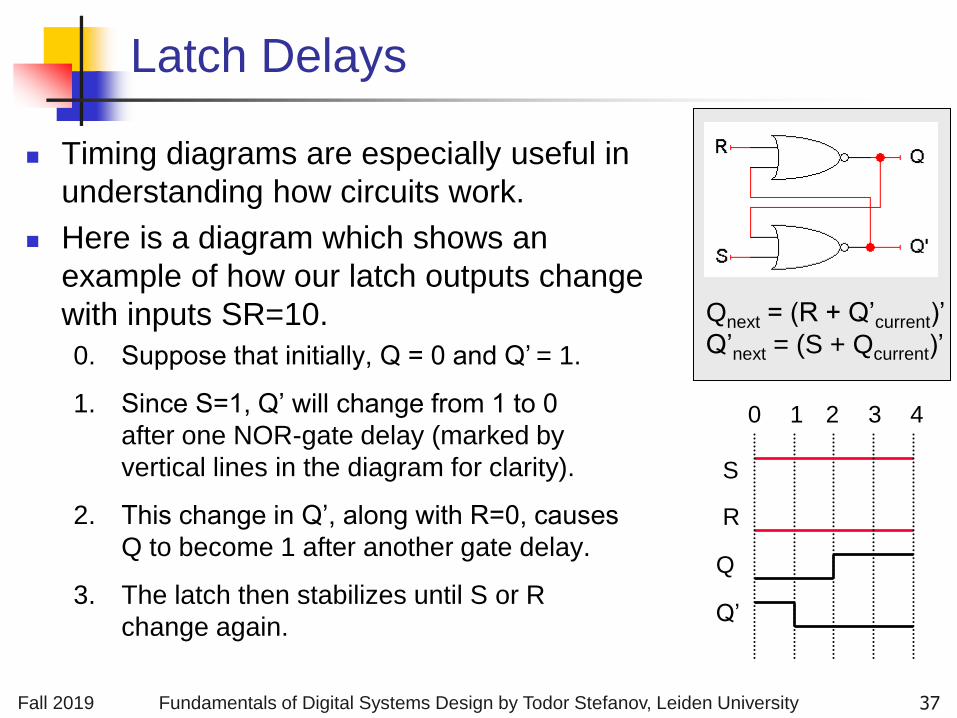
Latch Delays
Timing diagrams are especially useful in
understanding how circuits work.
Here is a diagram which shows an
example of how our latch outputs change
with inputs SR=10.
0. Suppose that initially, Q = 0 and Q’ = 1.
1. Since S=1, Q’ will change from 1 to 0
after one NOR-gate delay (marked by
vertical lines in the diagram for clarity).
2. This change in Q’, along with R=0, causes
Q to become 1 after another gate delay.
3. The latch then stabilizes until S or R
change again.
S
R
Q
Q’
0 1 2 3 4
Qnext = (R + Q’current)’
Q’next = (S + Qcurrent)’
37
Fall 2019 Fundamentals of Digital Systems Design by Todor Stefanov, Leiden University
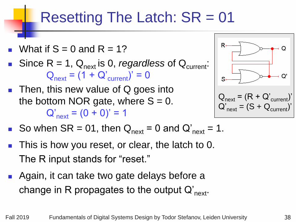
Resetting The Latch: SR = 01
What if S = 0 and R = 1?
Since R = 1, Qnext is 0, regardless of Qcurrent:
Qnext = (1 + Q’current)’ = 0
Then, this new value of Q goes into
the bottom NOR gate, where S = 0.
Q’next = (0 + 0)’ = 1
So when SR = 01, then Qnext = 0 and Q’next = 1.
This is how you reset, or clear, the latch to 0.
The R input stands for “reset.”
Again, it can take two gate delays before a
change in R propagates to the output Q’next.
Qnext = (R + Q’current)’
Q’next = (S + Qcurrent)’
38
Fall 2019 Fundamentals of Digital Systems Design by Todor Stefanov, Leiden University
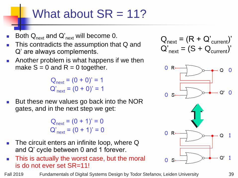
What about SR = 11?
Both Qnext and Q’next will become 0.
This contradicts the assumption that Q and Q’ are always complements.
Another problem is what happens if we then make S = 0 and R = 0 together.
Qnext = (0 + 0)’ = 1
Q’next = (0 + 0)’ = 1
But these new values go back into the NOR gates, and in the next step we get:
Qnext = (0 + 1)’ = 0
Q’next = (0 + 1)’ = 0
The circuit enters an infinite loop, where Q and Q’ cycle between 0 and 1 forever.
This is actually the worst case, but the moral is do not ever set SR=11!
Qnext = (R + Q’current)’
Q’next = (S + Qcurrent)’
0
0
0
0
0
0
1
1
39
Fall 2019 Fundamentals of Digital Systems Design by Todor Stefanov, Leiden University
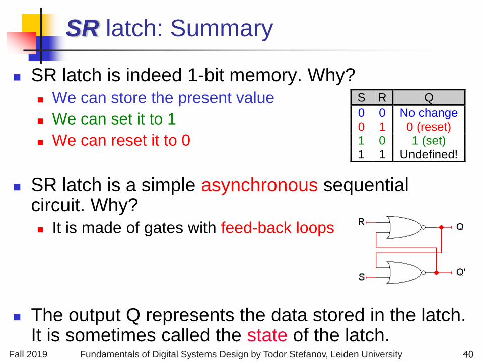
SR latch: Summary
SR latch is indeed 1-bit memory. Why? We can store the present value
We can set it to 1
We can reset it to 0
SR latch is a simple asynchronous sequential circuit. Why? It is made of gates with feed-back loops
The output Q represents the data stored in the latch. It is sometimes called the state of the latch.
S R Q
0 0 No change 0 1 0 (reset) 1 0 1 (set) 1 1 Undefined!
40
Fall 2019 Fundamentals of Digital Systems Design by Todor Stefanov, Leiden University
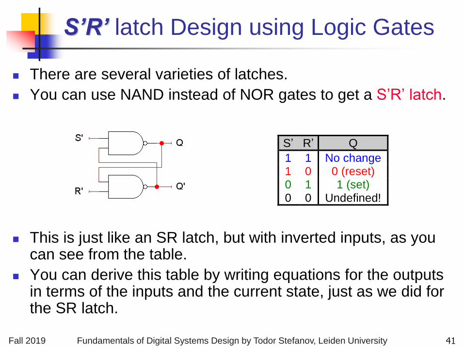
S’R’ latch Design using Logic Gates
There are several varieties of latches.
You can use NAND instead of NOR gates to get a S’R’ latch.
This is just like an SR latch, but with inverted inputs, as you can see from the table.
You can derive this table by writing equations for the outputs in terms of the inputs and the current state, just as we did for the SR latch.
S’ R’ Q
1 1 No change 1 0 0 (reset) 0 1 1 (set) 0 0 Undefined!
41
Fall 2019 Fundamentals of Digital Systems Design by Todor Stefanov, Leiden University
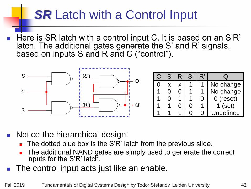
SR Latch with a Control Input
Here is SR latch with a control input C. It is based on an S’R’ latch. The additional gates generate the S’ and R’ signals, based on inputs S and R and C (“control”).
Notice the hierarchical design! The dotted blue box is the S’R’ latch from the previous slide.
The additional NAND gates are simply used to generate the correct inputs for the S’R’ latch.
The control input acts just like an enable.
C S R S’ R’ Q
0 x x 1 1 No change 1 0 0 1 1 No change 1 0 1 1 0 0 (reset) 1 1 0 0 1 1 (set) 1 1 1 0 0 Undefined
42
Fall 2019 Fundamentals of Digital Systems Design by Todor Stefanov, Leiden University
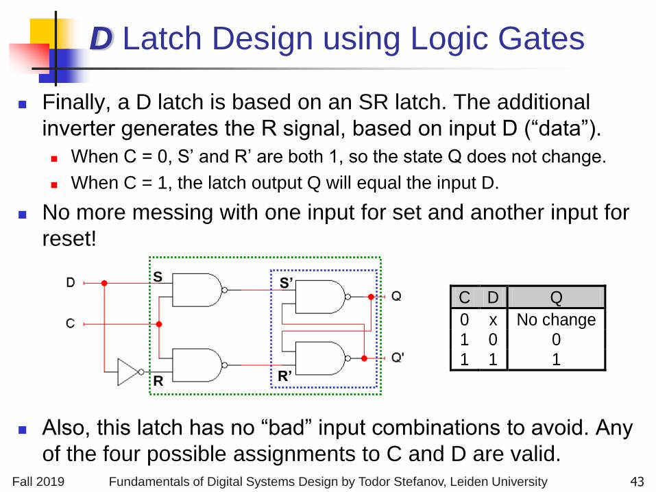
D Latch Design using Logic Gates
Finally, a D latch is based on an SR latch. The additional
inverter generates the R signal, based on input D (“data”).
When C = 0, S’ and R’ are both 1, so the state Q does not change.
When C = 1, the latch output Q will equal the input D.
No more messing with one input for set and another input for
reset!
Also, this latch has no “bad” input combinations to avoid. Any
of the four possible assignments to C and D are valid.
C D Q
0 x No change 1 0 0 1 1 1
S
R
S’
R’
43
Fall 2019 Fundamentals of Digital Systems Design by Todor Stefanov, Leiden University
Latches: Behaviour & Issues
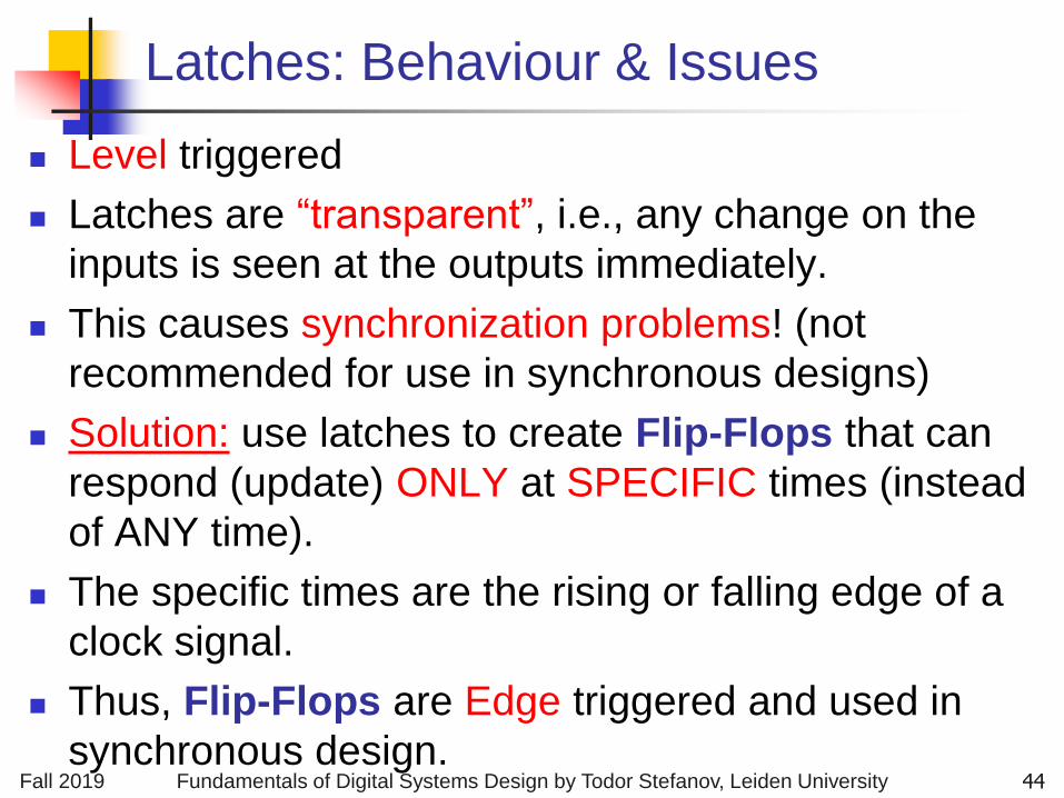
Level triggered
Latches are “transparent”, i.e., any change on the
inputs is seen at the outputs immediately.
This causes synchronization problems! (not
recommended for use in synchronous designs)
Solution: use latches to create Flip-Flops that can
respond (update) ONLY at SPECIFIC times (instead
of ANY time).
The specific times are the rising or falling edge of a
clock signal.
Thus, Flip-Flops are Edge triggered and used in
synchronous design. 44
Fall 2019 Fundamentals of Digital Systems Design by Todor Stefanov, Leiden University
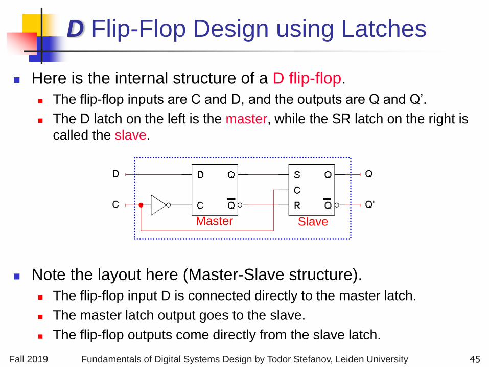
Here is the internal structure of a D flip-flop.
The flip-flop inputs are C and D, and the outputs are Q and Q’.
The D latch on the left is the master, while the SR latch on the right is
called the slave.
Note the layout here (Master-Slave structure).
The flip-flop input D is connected directly to the master latch.
The master latch output goes to the slave.
The flip-flop outputs come directly from the slave latch.
D Flip-Flop Design using Latches
Master Slave
45
Fall 2019 Fundamentals of Digital Systems Design by Todor Stefanov, Leiden University
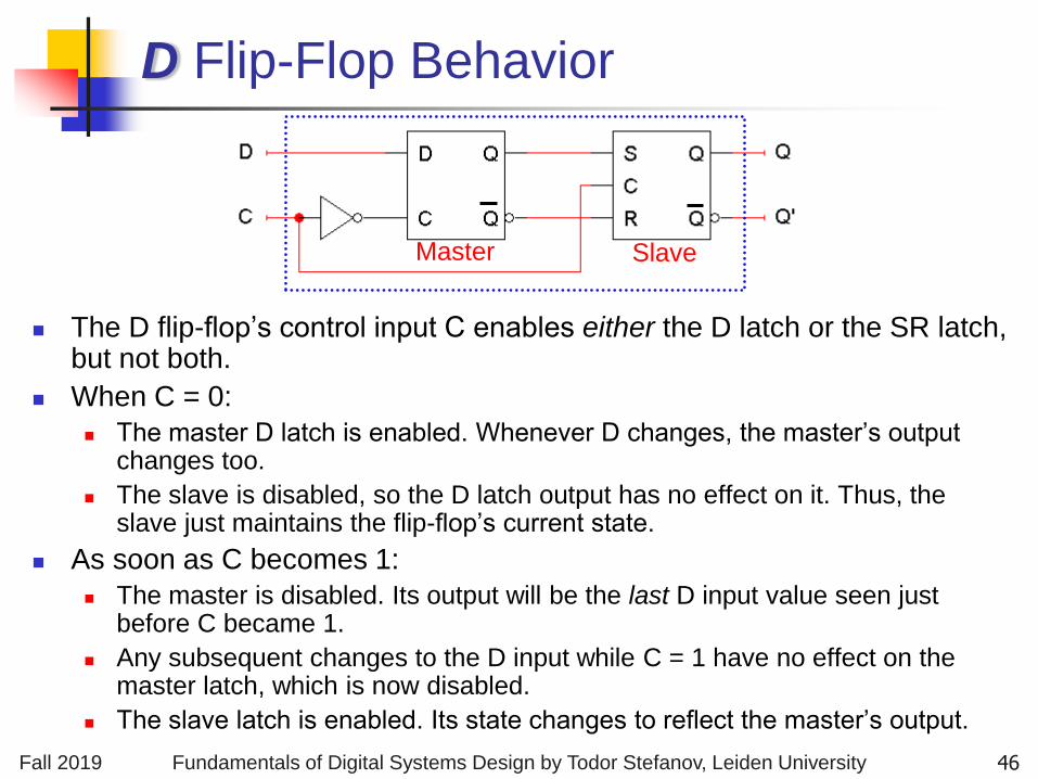
The D flip-flop’s control input C enables either the D latch or the SR latch, but not both.
When C = 0:
The master D latch is enabled. Whenever D changes, the master’s output changes too.
The slave is disabled, so the D latch output has no effect on it. Thus, the slave just maintains the flip-flop’s current state.
As soon as C becomes 1:
The master is disabled. Its output will be the last D input value seen just before C became 1.
Any subsequent changes to the D input while C = 1 have no effect on the master latch, which is now disabled.
The slave latch is enabled. Its state changes to reflect the master’s output.
D Flip-Flop Behavior
Master Slave
46
Fall 2019 Fundamentals of Digital Systems Design by Todor Stefanov, Leiden University
D Flip-Flop Behavior (cont.)
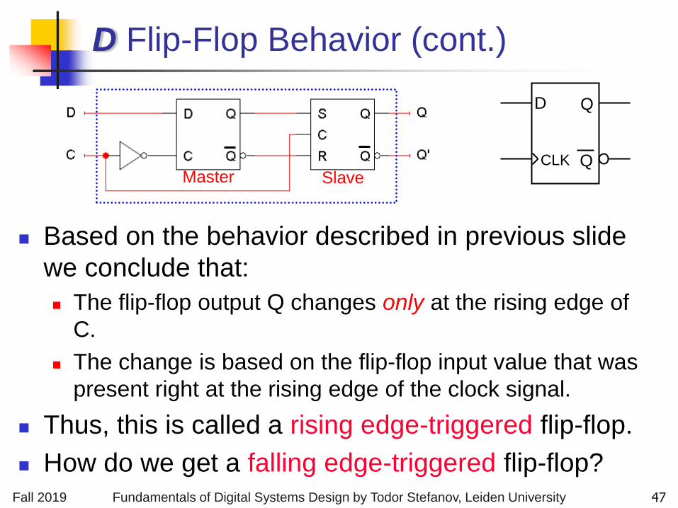
Based on the behavior described in previous slide
we conclude that:
The flip-flop output Q changes only at the rising edge of
C.
The change is based on the flip-flop input value that was
present right at the rising edge of the clock signal.
Thus, this is called a rising edge-triggered flip-flop.
How do we get a falling edge-triggered flip-flop?
Master Slave
D
CLK
Q
Q
47


![Haseeb Bokhari and Sri Parameswaranliacs.leidenuniv.nl/~stefanovtp/courses/ES/papers/... · on-chip communication is a key research area for multi-core architecture designers [17]](https://img.pdfslide.us/doc/110x75/60dc67a3865bed3f025e29ef/haseeb-bokhari-and-sri-stefanovtpcoursesespapers-on-chip-communication.jpg)