Embed Size (px)
Citation preview
Memories
Fall 2017 Digital Technique by Todor Stefanov, Leiden University
Overview
Memory Classification
Read-Only Memory (ROM)
Types of ROM
PROM, EPROM, E2PROM
Flash ROMs (Compact Flash, Secure Digital, Memory Stick)
Random Access Memory (RAM)
Types of RAM
Static RAM (SRAM) - ASRAM, SSRAM, ZBT
Dynamic RAM (DRAM) - SDRAM, DDR RAM, RDRAM
Functional Behavior of RAM
Introduction, Block Diagram, Memory Size
Reading/Writing from/to RAM
Implementing Static RAM
Making Larger and Wider Memory from Smaller Memories
Functional Behavior of ROM
Memories and Boolean Functions
2
Fall 2017 Digital Technique by Todor Stefanov, Leiden University
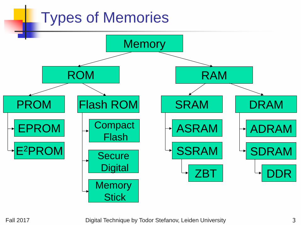
Types of Memories
Memory
ROM RAM
PROM Flash ROM
EPROM
E2PROM
Compact
Flash
Secure
Digital
Memory
Stick
SRAM DRAM
ASRAM
SSRAM
ZBT
3
ADRAM
SDRAM
DDR
Fall 2017 Digital Technique by Todor Stefanov, Leiden University
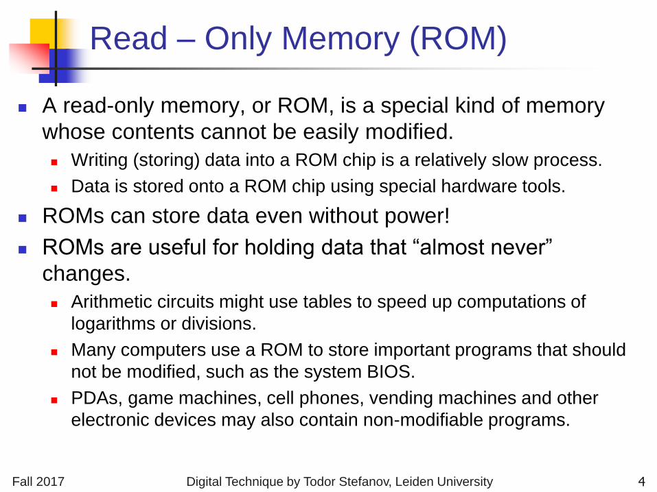
Read – Only Memory (ROM)
A read-only memory, or ROM, is a special kind of memory
whose contents cannot be easily modified.
Writing (storing) data into a ROM chip is a relatively slow process.
Data is stored onto a ROM chip using special hardware tools.
ROMs can store data even without power!
ROMs are useful for holding data that “almost never”
changes.
Arithmetic circuits might use tables to speed up computations of
logarithms or divisions.
Many computers use a ROM to store important programs that should
not be modified, such as the system BIOS.
PDAs, game machines, cell phones, vending machines and other
electronic devices may also contain non-modifiable programs.
4
Fall 2017 Digital Technique by Todor Stefanov, Leiden University
PROM (Programmable ROM) It can be programmed (written) only once.
EPROM (Electrical Programmable ROM) It can be programmed a limited number of times.
Before reprogramming the memory you must erase it with ultraviolet waves.
E2PROM (Electrical Erasable Programmable ROM) The same as EPROM but
You can erase it by applying electrical pulses on special pins.
Programming (writing) and erasing the above memories is a very slow process. It may take seconds or minutes!
Types of ROMs
5
Fall 2017 Digital Technique by Todor Stefanov, Leiden University
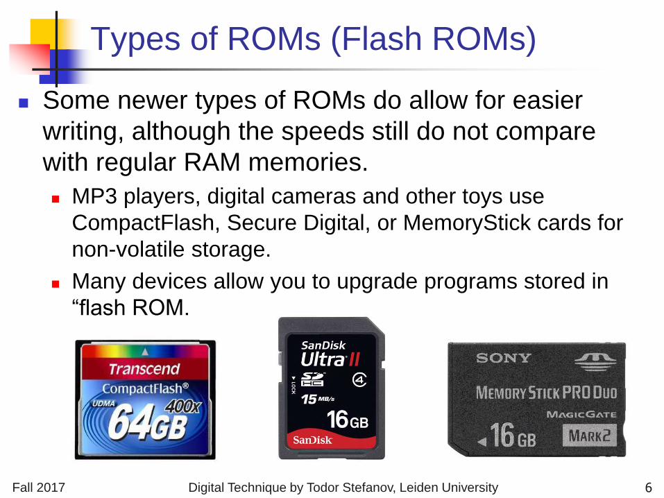
Types of ROMs (Flash ROMs)
Some newer types of ROMs do allow for easier
writing, although the speeds still do not compare
with regular RAM memories.
MP3 players, digital cameras and other toys use
CompactFlash, Secure Digital, or MemoryStick cards for
non-volatile storage.
Many devices allow you to upgrade programs stored in
“flash ROM.
6
Fall 2017 Digital Technique by Todor Stefanov, Leiden University
Random Access Memory (RAM)
RAM is a kind of memory whose contents can be
easily modified.
Writing (storing) data into a RAM chip is as faster as
reading data.
No special hardware tools are needed to store the data in
the RAM.
RAMs cannot store data without power!
RAMs are useful for storing temporary data that has
to be modified very often.
Many computers use RAM for storing the currently
executed program and/or intermediate data.
The CPU cache memory is a RAM memory.
7
Fall 2017 Digital Technique by Todor Stefanov, Leiden University
Types of RAMs
SRAM (Static RAM) It is build using Latches
Expensive in terms of hardware
For each bit of storage you need 6 transistors
Very fast memory
DRAM (Dynamic RAM) Dynamic memory is built with capacitors.
A stored charge on the capacitor represents a logical 1.
No charge represents a logic 0.
However, capacitors lose their charge after a few milliseconds. The memory requires constant refreshing to recharge the capacitors. (That’s what’s “dynamic” about it.)
Dynamic RAMs tend to be physically smaller than static RAMs.
A single bit of data can be stored with just one capacitor and one transistor, while static RAM cells typically require 4-6 transistors.
This means dynamic RAM is cheaper and denser—more bits can be stored in the same physical area.
8
Fall 2017 Digital Technique by Todor Stefanov, Leiden University
Dynamic vs. Static Memory
In practice, dynamic RAM is used for a computer’s main memory, since it is cheap and you can pack a lot of storage into a small space These days you can buy 1 GB of memory for as little as $15
You can have a system with 8 GB or more of memory (up to 128GB)
The disadvantage of dynamic RAM is its speed Up to 1.2GHz, which can be slower than the processor itself
You also have to consider latency, or the time it takes data to travel from RAM to the processor
Real systems augment dynamic memory with small but fast sections of static memory called caches. Typical processor caches range in size from 128KB to 4MB
That is small compared to a 8 GB main memory, but it is enough to significantly increase a computer’s overall speed
9
Fall 2017 Digital Technique by Todor Stefanov, Leiden University
Types of SRAM
ASRAM (Asynchronous Static RAM)
no clock signal is used when reading/writing data
SSRAM (Synchronous Static RAM)
read and write from/to the memory is synchronized by a
clock signal
ZBT (Zero-Bus Turnaround) SSRAM
Very fast memory
See more details on Internet
10
Fall 2017 Digital Technique by Todor Stefanov, Leiden University
Types of DRAM
ADRAM (Asynchronous Dynamic RAM)
older type of DRAM used in the early personal computers
memory access is not synchronized with the system clock
SDRAM (Synchronous Dynamic RAM)
widely used nowadays
responds to read/write operations in synchrony with the
signal of the system clock
DDR SDRAM (Double Data Rate SDRAM)
11
Fall 2017 Digital Technique by Todor Stefanov, Leiden University
SDRAM
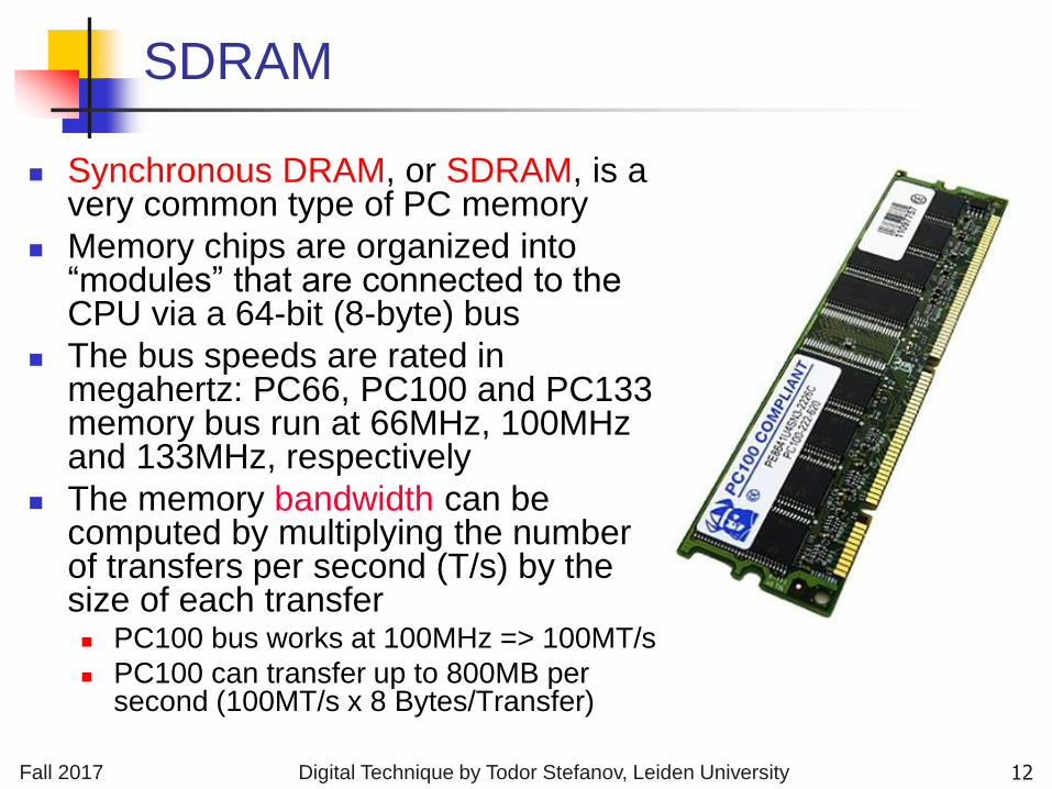
Synchronous DRAM, or SDRAM, is a very common type of PC memory
Memory chips are organized into “modules” that are connected to the CPU via a 64-bit (8-byte) bus
The bus speeds are rated in megahertz: PC66, PC100 and PC133 memory bus run at 66MHz, 100MHz and 133MHz, respectively
The memory bandwidth can be computed by multiplying the number of transfers per second (T/s) by the size of each transfer PC100 bus works at 100MHz => 100MT/s
PC100 can transfer up to 800MB per second (100MT/s x 8 Bytes/Transfer)
12
Fall 2017 Digital Technique by Todor Stefanov, Leiden University
DDR SDRAM
A newer type of memory is Double Data Rate, or DDR-SDRAM Several generations from DDR2 to DDR4
It is very similar to regular SDRAM, except data can be transferred on both the positive and negative clock edges
DDR4 memory bus runs at 800-1200MHz but the effective data transfer rate is doubled, i.e., 1600-2400MT/s
These memories are called PC4-1600 and PC4-2400 with bandwidth Up to 12800MB/s = 1600MT/s x 8 Bytes/Transfer
Up to 19200MB/s = 2400MT/s x 8 Bytes/Transfer
DDR-SDRAM has lower power consumption, using 1.2-2.5V instead of 3.3V like SDRAM. This makes it good for notebooks and other mobile devices
13
Fall 2017 Digital Technique by Todor Stefanov, Leiden University
ROMs vs. RAMs
There are some important differences between
ROM and RAM.
ROMs are “non-volatile”
data is preserved even without power
RAM contents disappear once power is lost.
ROMs require special (and slower) techniques for writing,
so they are considered to be “read-only” devices.
14
Fall 2017 Digital Technique by Todor Stefanov, Leiden University
Random Access Memory (RAM)
Sequential circuits all depend upon the presence of
memory.
A flip-flop can store one bit of information.
A register can store a single “word,” typically 32-64 bits.
Random access memory, or RAM, allows us to
store even larger amounts of data. Today you will
see:
The basic interface to RAM memory.
How you can implement static RAM chips hierarchically.
15
Fall 2017 Digital Technique by Todor Stefanov, Leiden University
Introduction to RAM
Random-access memory, or RAM, provides large quantities of temporary storage in a computer system.
Remember the basic properties of a memory: It should be able to store a value.
You should be able to read the value that was stored.
You should be able to change the stored value.
A RAM is similar, except that it can store many values. An address will specify which memory value we are interested in.
Each value can be a multiple-bit word (e.g., 32 bits).
We will refine the memory properties as follows:
A RAM should be able to:
- Store many words (values), one per address
- Read the word that was stored at a particular address
- Change the word that was stored at a particular address
16
Fall 2017 Digital Technique by Todor Stefanov, Leiden University
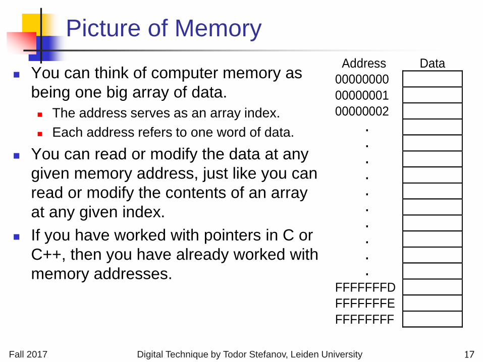
Picture of Memory
You can think of computer memory as
being one big array of data.
The address serves as an array index.
Each address refers to one word of data.
You can read or modify the data at any
given memory address, just like you can
read or modify the contents of an array
at any given index.
If you have worked with pointers in C or
C++, then you have already worked with
memory addresses.
Address Data
00000000
00000001
00000002
.
.
.
.
.
.
.
.
.
.
FFFFFFFD
FFFFFFFE
FFFFFFFF
17
Fall 2017 Digital Technique by Todor Stefanov, Leiden University
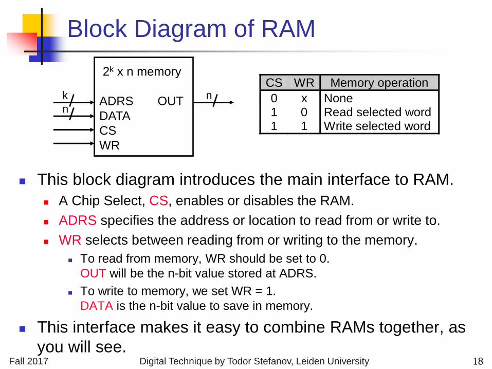
Block Diagram of RAM
This block diagram introduces the main interface to RAM.
A Chip Select, CS, enables or disables the RAM.
ADRS specifies the address or location to read from or write to.
WR selects between reading from or writing to the memory.
To read from memory, WR should be set to 0.
OUT will be the n-bit value stored at ADRS.
To write to memory, we set WR = 1.
DATA is the n-bit value to save in memory.
This interface makes it easy to combine RAMs together, as
you will see.
2k x n memory
ADRS OUT
DATA
CS
WR
k
n
n CS WR Memory operation
0 x None 1 0 Read selected word 1 1 Write selected word
18
Fall 2017 Digital Technique by Todor Stefanov, Leiden University
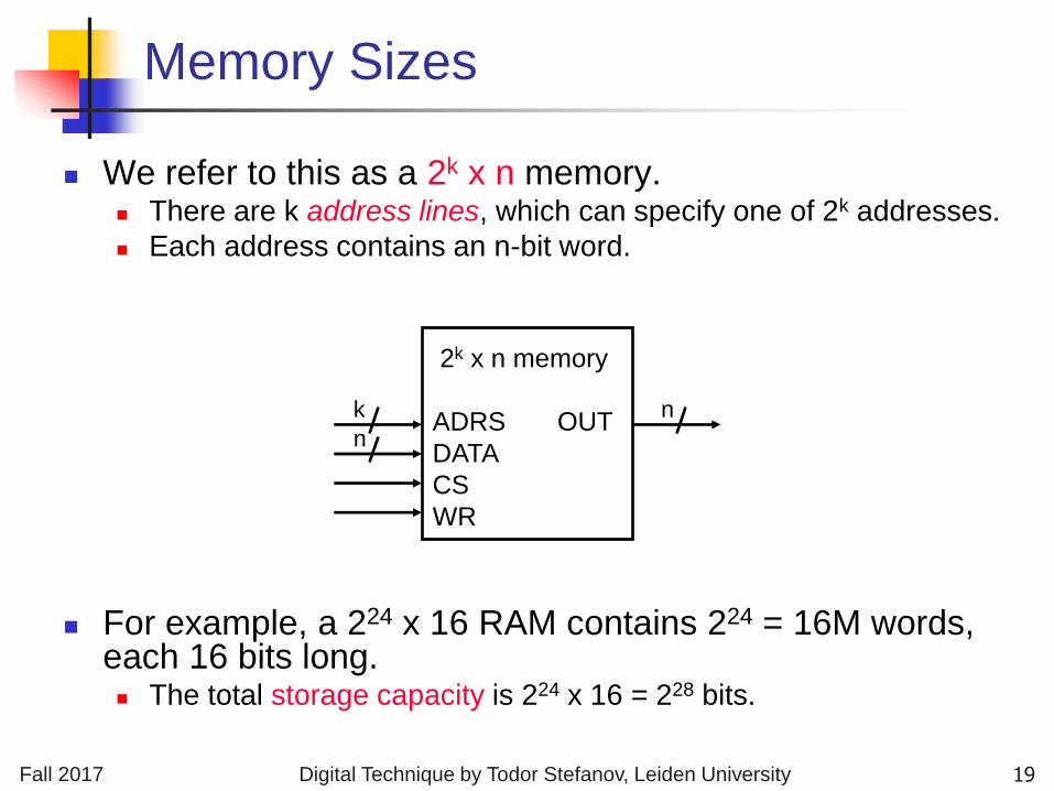
Memory Sizes
We refer to this as a 2k x n memory. There are k address lines, which can specify one of 2k addresses.
Each address contains an n-bit word.
For example, a 224 x 16 RAM contains 224 = 16M words, each 16 bits long. The total storage capacity is 224 x 16 = 228 bits.
2k x n memory
ADRS OUT
DATA
CS
WR
k
n
n
19
Fall 2017 Digital Technique by Todor Stefanov, Leiden University
Size Matters!
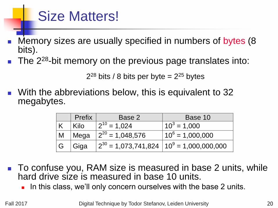
Memory sizes are usually specified in numbers of bytes (8 bits).
The 228-bit memory on the previous page translates into:
228 bits / 8 bits per byte = 225 bytes
With the abbreviations below, this is equivalent to 32 megabytes.
To confuse you, RAM size is measured in base 2 units, while hard drive size is measured in base 10 units. In this class, we’ll only concern ourselves with the base 2 units.
Prefix Base 2 Base 10
K Kilo 210 = 1,024 103 = 1,000
M Mega 220 = 1,048,576 106 = 1,000,000
G Giga 230 = 1,073,741,824 109 = 1,000,000,000
20
Fall 2017 Digital Technique by Todor Stefanov, Leiden University
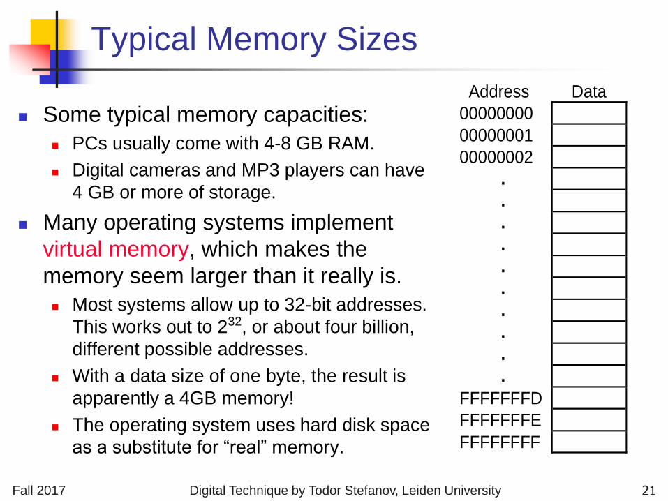
Typical Memory Sizes
Some typical memory capacities:
PCs usually come with 4-8 GB RAM.
Digital cameras and MP3 players can have
4 GB or more of storage.
Many operating systems implement
virtual memory, which makes the
memory seem larger than it really is.
Most systems allow up to 32-bit addresses.
This works out to 232, or about four billion,
different possible addresses.
With a data size of one byte, the result is
apparently a 4GB memory!
The operating system uses hard disk space
as a substitute for “real” memory.
Address Data
00000000
00000001
00000002
.
.
.
.
.
.
.
.
.
.
FFFFFFFD
FFFFFFFE
FFFFFFFF
21
Fall 2017 Digital Technique by Todor Stefanov, Leiden University
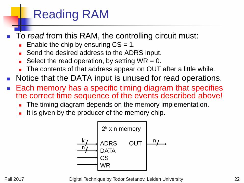
Reading RAM
To read from this RAM, the controlling circuit must: Enable the chip by ensuring CS = 1.
Send the desired address to the ADRS input.
Select the read operation, by setting WR = 0.
The contents of that address appear on OUT after a little while.
Notice that the DATA input is unused for read operations.
Each memory has a specific timing diagram that specifies the correct time sequence of the events described above! The timing diagram depends on the memory implementation.
It is given by the producer of the memory chip.
2k x n memory
ADRS OUT
DATA
CS
WR
k
n
n
22
Fall 2017 Digital Technique by Todor Stefanov, Leiden University
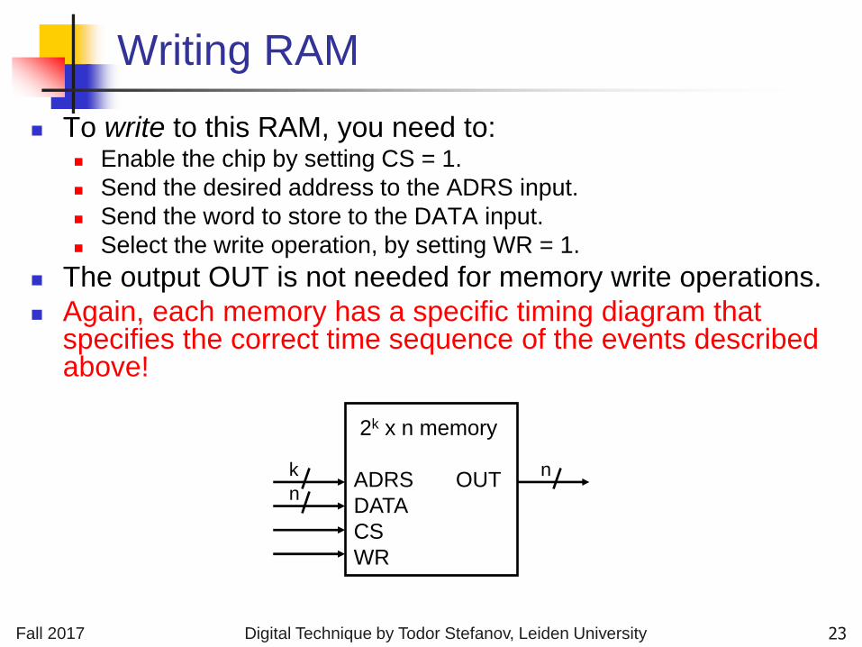
Writing RAM
To write to this RAM, you need to: Enable the chip by setting CS = 1.
Send the desired address to the ADRS input.
Send the word to store to the DATA input.
Select the write operation, by setting WR = 1.
The output OUT is not needed for memory write operations.
Again, each memory has a specific timing diagram that specifies the correct time sequence of the events described above!
2k x n memory
ADRS OUT
DATA
CS
WR
k
n
n
23
Fall 2017 Digital Technique by Todor Stefanov, Leiden University
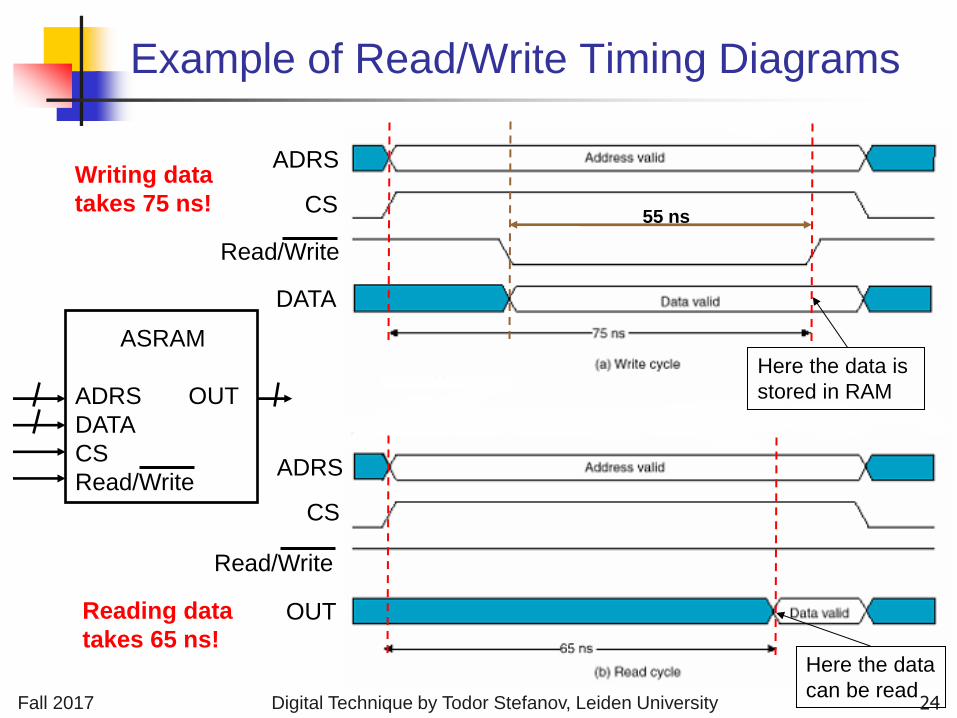
Example of Read/Write Timing Diagrams
ASRAM
ADRS OUT
DATA
CS
Read/Write
ADRS
CS
Read/Write
DATA
55 ns
ADRS
CS
Read/Write
OUT
Here the data is
stored in RAM
Here the data
can be read
Writing data
takes 75 ns!
Reading data
takes 65 ns!
24
Fall 2017 Digital Technique by Todor Stefanov, Leiden University
Static Memory
How can we implement the memory chip?
There are many different kinds of RAM. We will discuss only static memory, which is most
commonly used in caches and video cards.
Static memory is modeled using one latch for each bit of storage.
Why use latches instead of flip-flops? A latch can be made with only two NAND or two NOR
gates, but a flip-flop requires at least twice that much hardware.
In general, smaller is faster, cheaper and requires less power.
The tradeoff is that getting the timing exactly right is a pain.
25
Fall 2017 Digital Technique by Todor Stefanov, Leiden University
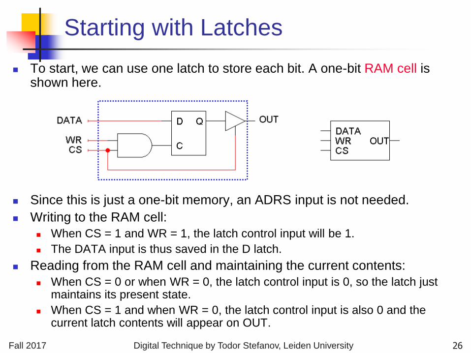
Starting with Latches
To start, we can use one latch to store each bit. A one-bit RAM cell is shown here.
Since this is just a one-bit memory, an ADRS input is not needed.
Writing to the RAM cell:
When CS = 1 and WR = 1, the latch control input will be 1.
The DATA input is thus saved in the D latch.
Reading from the RAM cell and maintaining the current contents:
When CS = 0 or when WR = 0, the latch control input is 0, so the latch just maintains its present state.
When CS = 1 and when WR = 0, the latch control input is also 0 and the current latch contents will appear on OUT.
26
Fall 2017 Digital Technique by Todor Stefanov, Leiden University
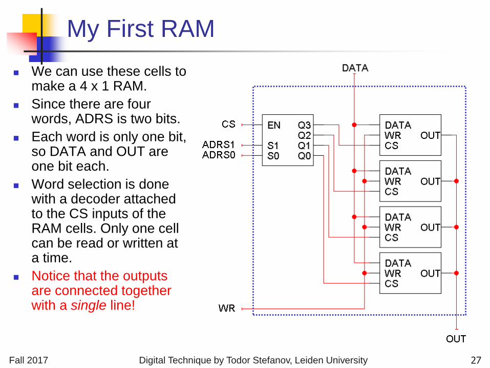
My First RAM
We can use these cells to make a 4 x 1 RAM.
Since there are four words, ADRS is two bits.
Each word is only one bit, so DATA and OUT are one bit each.
Word selection is done with a decoder attached to the CS inputs of the RAM cells. Only one cell can be read or written at a time.
Notice that the outputs are connected together with a single line!
27
Fall 2017 Digital Technique by Todor Stefanov, Leiden University
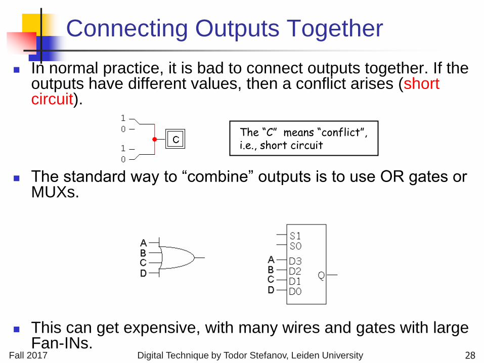
In normal practice, it is bad to connect outputs together. If the outputs have different values, then a conflict arises (short circuit).
The standard way to “combine” outputs is to use OR gates or MUXs.
This can get expensive, with many wires and gates with large Fan-INs.
Connecting Outputs Together
The “C” means “conflict”, i.e., short circuit
28
Fall 2017 Digital Technique by Todor Stefanov, Leiden University
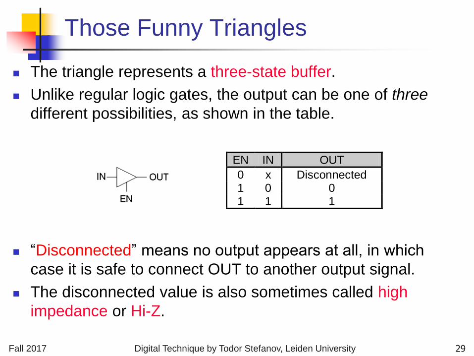
Those Funny Triangles
The triangle represents a three-state buffer.
Unlike regular logic gates, the output can be one of three
different possibilities, as shown in the table.
“Disconnected” means no output appears at all, in which
case it is safe to connect OUT to another output signal.
The disconnected value is also sometimes called high
impedance or Hi-Z.
EN IN OUT
0 x Disconnected 1 0 0 1 1 1
29
Fall 2017 Digital Technique by Todor Stefanov, Leiden University
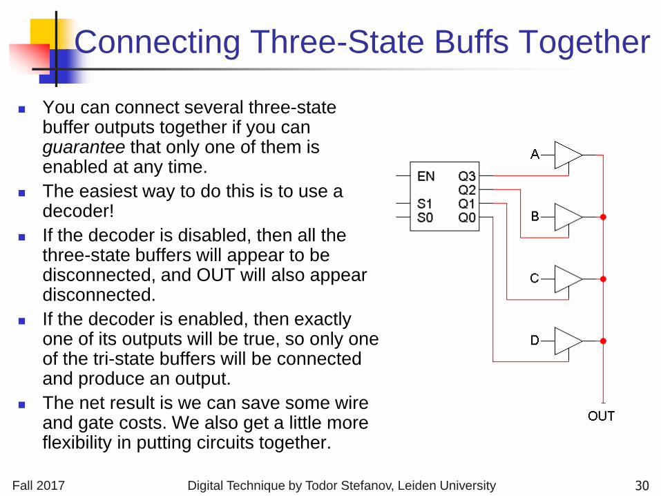
Connecting Three-State Buffs Together
You can connect several three-state buffer outputs together if you can guarantee that only one of them is enabled at any time.
The easiest way to do this is to use a decoder!
If the decoder is disabled, then all the three-state buffers will appear to be disconnected, and OUT will also appear disconnected.
If the decoder is enabled, then exactly one of its outputs will be true, so only one of the tri-state buffers will be connected and produce an output.
The net result is we can save some wire and gate costs. We also get a little more flexibility in putting circuits together.
30
Fall 2017 Digital Technique by Todor Stefanov, Leiden University
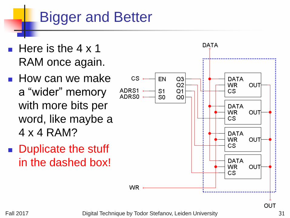
Bigger and Better
Here is the 4 x 1
RAM once again.
How can we make
a “wider” memory
with more bits per
word, like maybe a
4 x 4 RAM?
Duplicate the stuff
in the dashed box!
31
Fall 2017 Digital Technique by Todor Stefanov, Leiden University
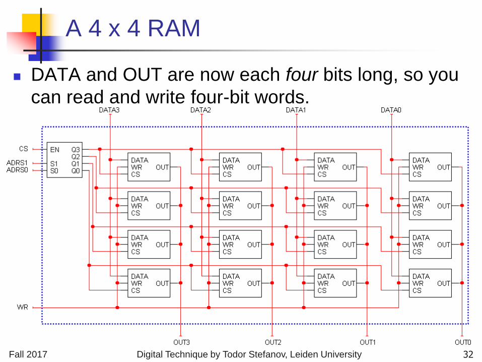
A 4 x 4 RAM
DATA and OUT are now each four bits long, so you
can read and write four-bit words.
32
Fall 2017 Digital Technique by Todor Stefanov, Leiden University
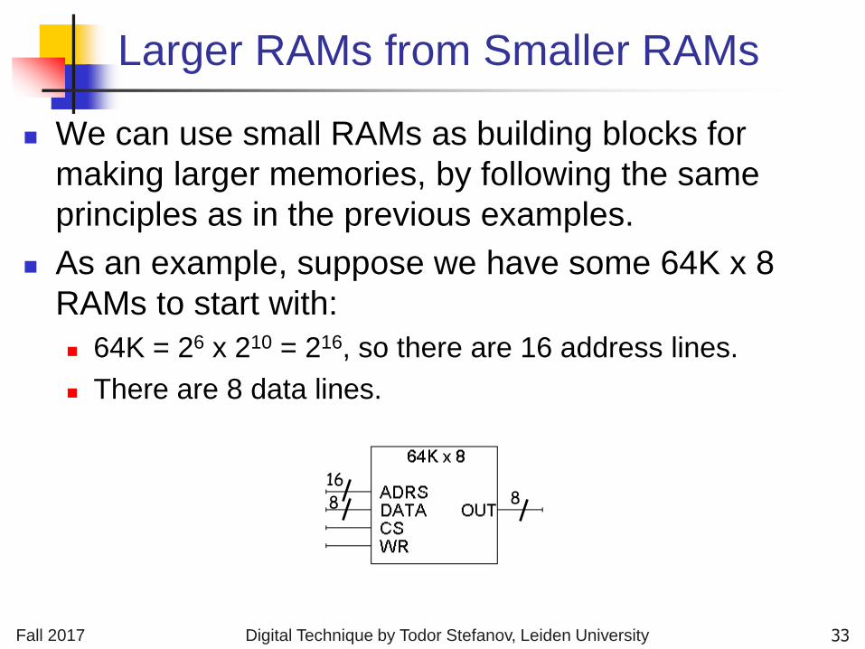
Larger RAMs from Smaller RAMs
We can use small RAMs as building blocks for
making larger memories, by following the same
principles as in the previous examples.
As an example, suppose we have some 64K x 8
RAMs to start with:
64K = 26 x 210 = 216, so there are 16 address lines.
There are 8 data lines.
8 8 16
33
Fall 2017 Digital Technique by Todor Stefanov, Leiden University
8
8
16
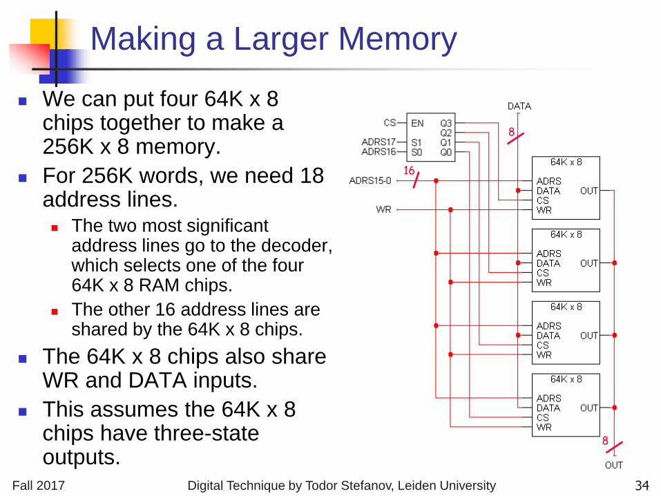
Making a Larger Memory
We can put four 64K x 8 chips together to make a 256K x 8 memory.
For 256K words, we need 18 address lines. The two most significant
address lines go to the decoder, which selects one of the four 64K x 8 RAM chips.
The other 16 address lines are shared by the 64K x 8 chips.
The 64K x 8 chips also share WR and DATA inputs.
This assumes the 64K x 8 chips have three-state outputs.
34
Fall 2017 Digital Technique by Todor Stefanov, Leiden University
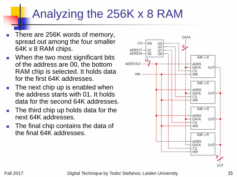
Analyzing the 256K x 8 RAM
There are 256K words of memory, spread out among the four smaller 64K x 8 RAM chips.
When the two most significant bits of the address are 00, the bottom RAM chip is selected. It holds data for the first 64K addresses.
The next chip up is enabled when the address starts with 01. It holds data for the second 64K addresses.
The third chip up holds data for the next 64K addresses.
The final chip contains the data of the final 64K addresses.
8
8
16
35
Fall 2017 Digital Technique by Todor Stefanov, Leiden University
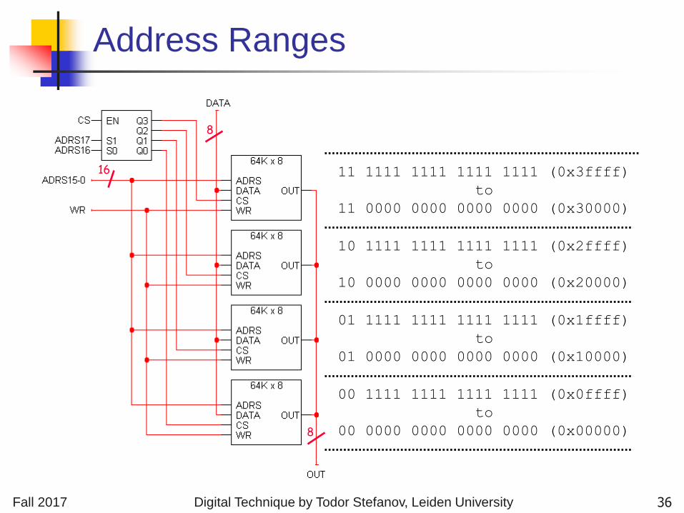
Address Ranges
8
8
16 11 1111 1111 1111 1111 (0x3ffff)
to
11 0000 0000 0000 0000 (0x30000)
10 1111 1111 1111 1111 (0x2ffff)
to
10 0000 0000 0000 0000 (0x20000)
01 1111 1111 1111 1111 (0x1ffff)
to
01 0000 0000 0000 0000 (0x10000)
00 1111 1111 1111 1111 (0x0ffff)
to
00 0000 0000 0000 0000 (0x00000)
36
Fall 2017 Digital Technique by Todor Stefanov, Leiden University
16
8 8
8 8
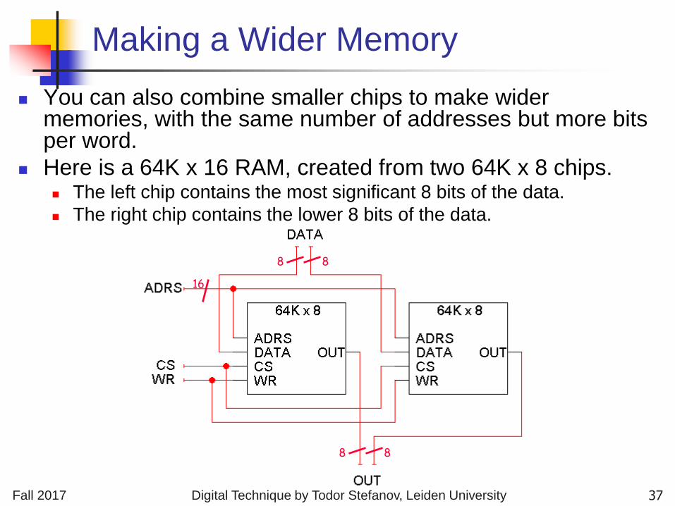
Making a Wider Memory
You can also combine smaller chips to make wider memories, with the same number of addresses but more bits per word.
Here is a 64K x 16 RAM, created from two 64K x 8 chips. The left chip contains the most significant 8 bits of the data.
The right chip contains the lower 8 bits of the data.
37
Fall 2017 Digital Technique by Todor Stefanov, Leiden University
Summary
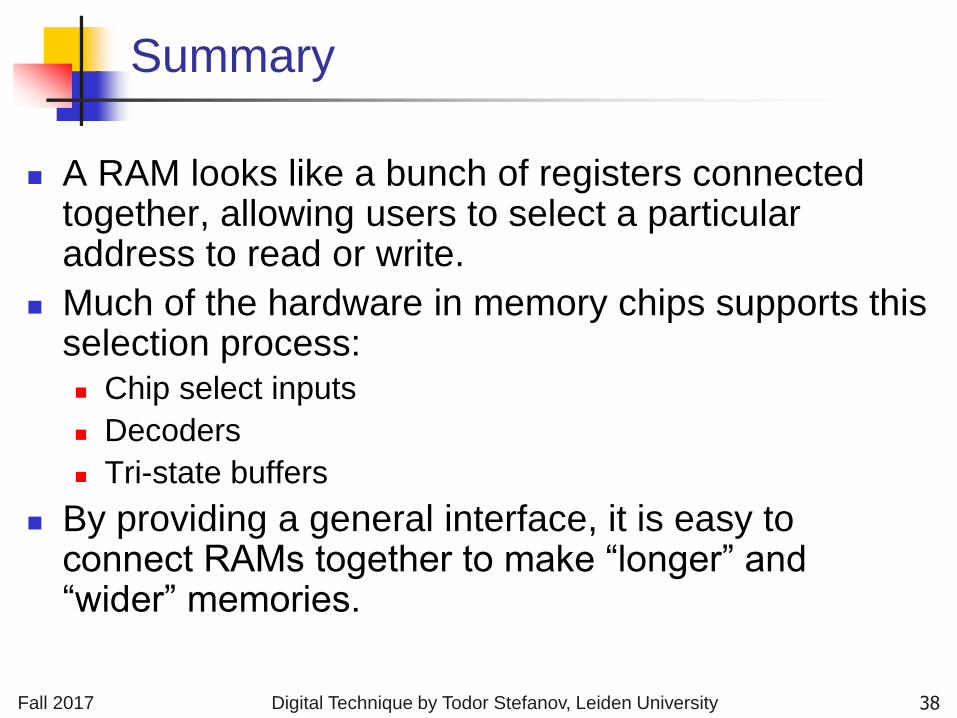
A RAM looks like a bunch of registers connected together, allowing users to select a particular address to read or write.
Much of the hardware in memory chips supports this selection process: Chip select inputs
Decoders
Tri-state buffers
By providing a general interface, it is easy to connect RAMs together to make “longer” and “wider” memories.
38
Fall 2017 Digital Technique by Todor Stefanov, Leiden University
Read-Only Memory
2k x n ROM
ADDR OUT
CS
k n
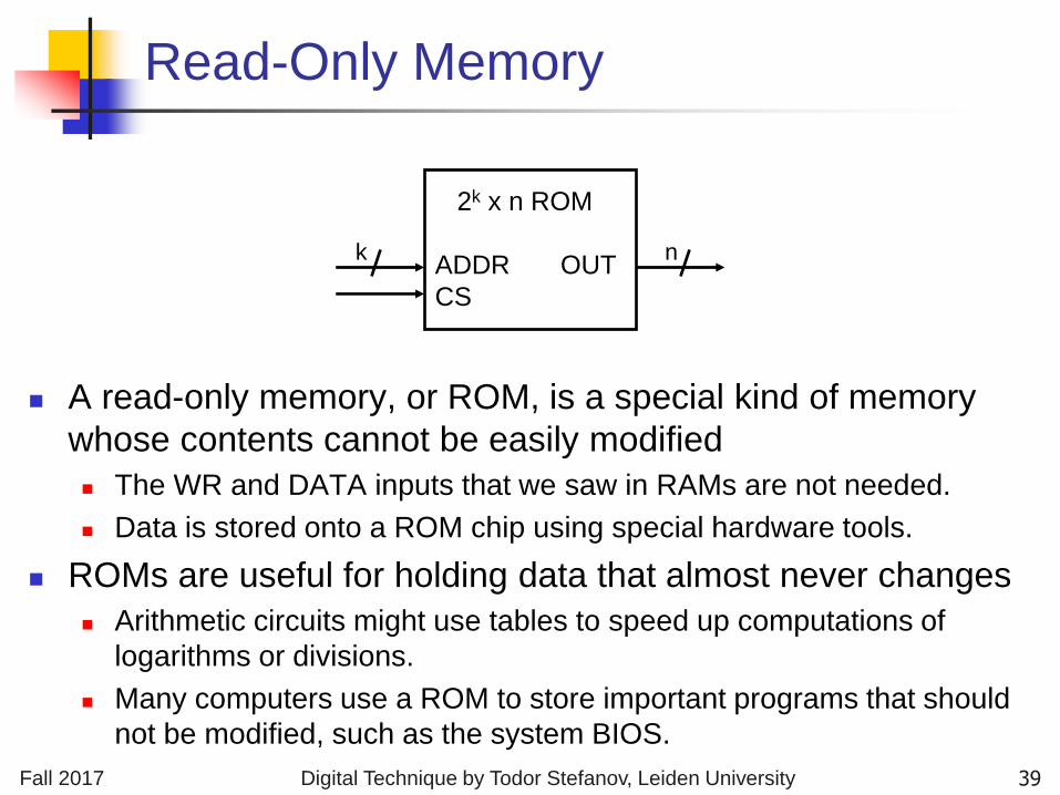
A read-only memory, or ROM, is a special kind of memory
whose contents cannot be easily modified
The WR and DATA inputs that we saw in RAMs are not needed.
Data is stored onto a ROM chip using special hardware tools.
ROMs are useful for holding data that almost never changes
Arithmetic circuits might use tables to speed up computations of
logarithms or divisions.
Many computers use a ROM to store important programs that should
not be modified, such as the system BIOS.
39
Fall 2017 Digital Technique by Todor Stefanov, Leiden University
Memories and Functions
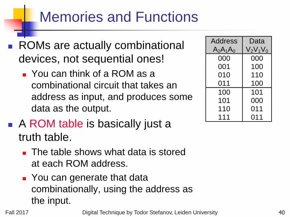
ROMs are actually combinational
devices, not sequential ones!
You can think of a ROM as a
combinational circuit that takes an
address as input, and produces some
data as the output.
A ROM table is basically just a
truth table.
The table shows what data is stored
at each ROM address.
You can generate that data
combinationally, using the address as
the input.
Address A2A1A0
Data V2V1V0
000 000 001 100 010 110 011 100
100 101 101 000 110 011 111 011
40
Fall 2017 Digital Technique by Todor Stefanov, Leiden University
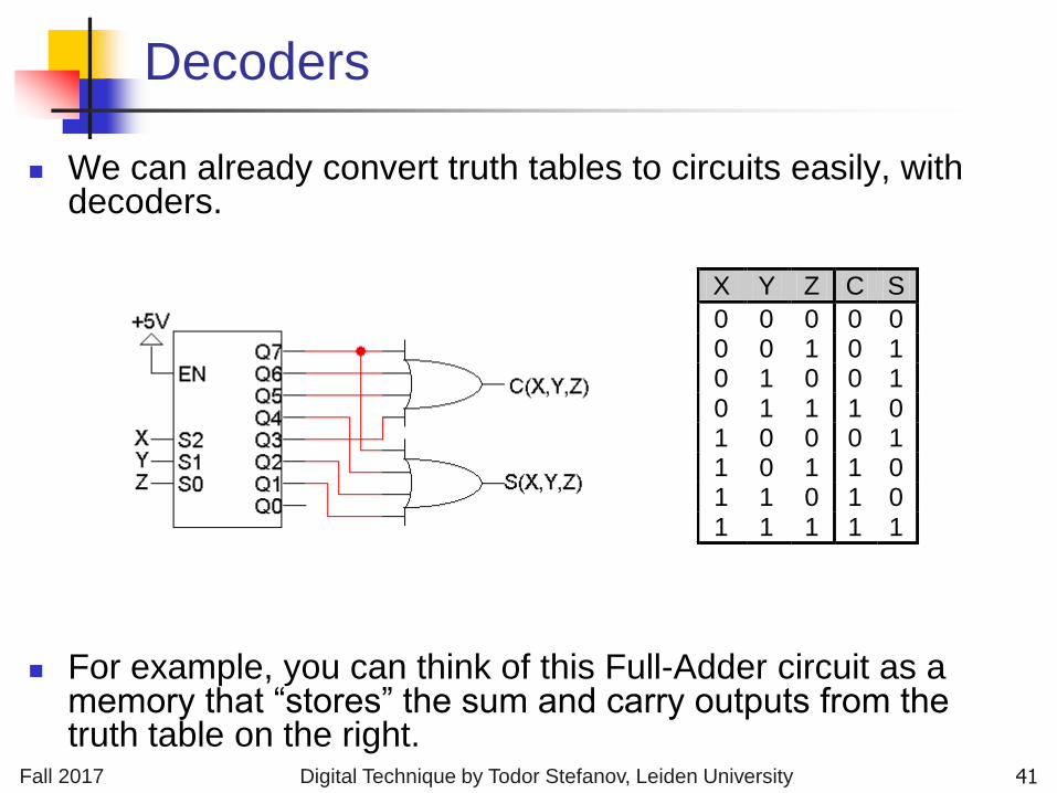
Decoders
We can already convert truth tables to circuits easily, with decoders.
For example, you can think of this Full-Adder circuit as a memory that “stores” the sum and carry outputs from the truth table on the right.
X Y Z C S
0 0 0 0 0 0 0 1 0 1 0 1 0 0 1 0 1 1 1 0 1 0 0 0 1 1 0 1 1 0 1 1 0 1 0 1 1 1 1 1
41
Fall 2017 Digital Technique by Todor Stefanov, Leiden University
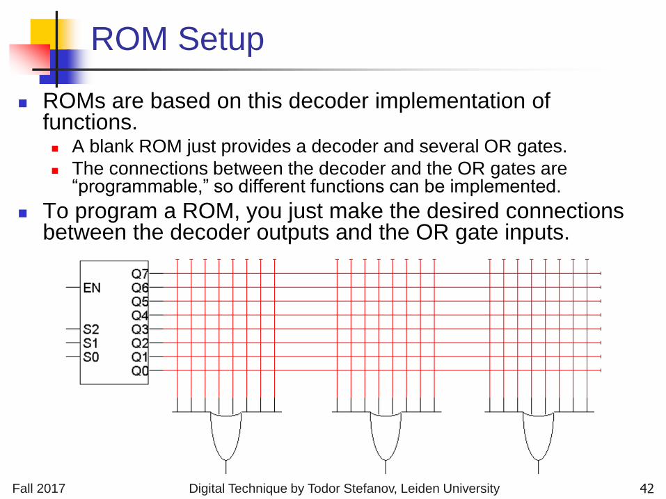
ROM Setup
ROMs are based on this decoder implementation of functions. A blank ROM just provides a decoder and several OR gates.
The connections between the decoder and the OR gates are “programmable,” so different functions can be implemented.
To program a ROM, you just make the desired connections between the decoder outputs and the OR gate inputs.
42
Fall 2017 Digital Technique by Todor Stefanov, Leiden University
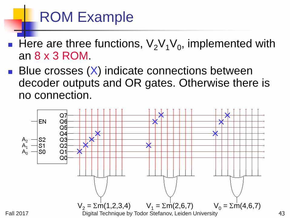
ROM Example
Here are three functions, V2V1V0, implemented with an 8 x 3 ROM.
Blue crosses (X) indicate connections between decoder outputs and OR gates. Otherwise there is no connection.
V2 = m(1,2,3,4) V1 = m(2,6,7) V0 = m(4,6,7)
A2 A1 A0
43
Fall 2017 Digital Technique by Todor Stefanov, Leiden University
V2 V1 V0
A2 A1 A0
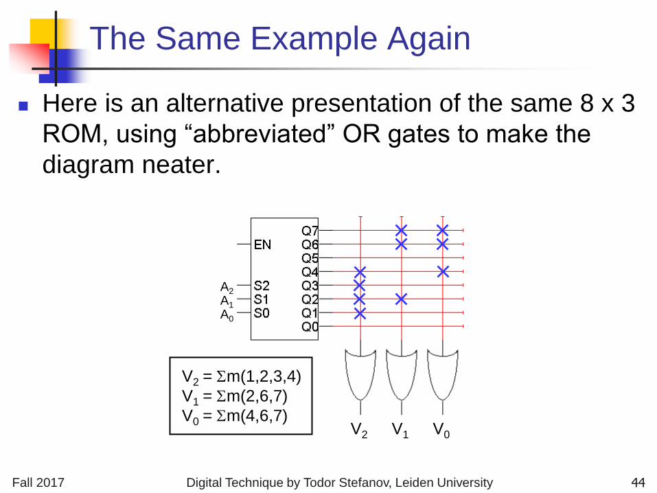
The Same Example Again
Here is an alternative presentation of the same 8 x 3
ROM, using “abbreviated” OR gates to make the
diagram neater.
V2 = m(1,2,3,4)
V1 = m(2,6,7)
V0 = m(4,6,7)
44
Fall 2017 Digital Technique by Todor Stefanov, Leiden University
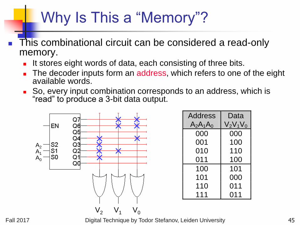
Why Is This a “Memory”?
This combinational circuit can be considered a read-only memory. It stores eight words of data, each consisting of three bits.
The decoder inputs form an address, which refers to one of the eight available words.
So, every input combination corresponds to an address, which is “read” to produce a 3-bit data output.
V2 V1 V0
A2 A1 A0
Address A2A1A0
Data V2V1V0
000 000 001 100 010 110 011 100
100 101 101 000 110 011 111 011
45
Fall 2017 Digital Technique by Todor Stefanov, Leiden University
Functions and Memories
ROMs give us another way to implement
functions.
The idea behind using a ROM to implement a
function is to “store” the function’s truth table,
so we do not have to do any (well, very little)
computation.
This is like “memorization” or “caching”
techniques in programming.
46
Fall 2017 Digital Technique by Todor Stefanov, Leiden University
Summary
We discussed RAM and ROM memories.
There are two main kinds of RAM memory.
Static RAM
costs more in terms of HW, but the memory is faster
often used to implement cache memories
Dynamic RAM
costs less HW and requires less physical space
making it ideal for larger-capacity memories
access times are slower
ROMs are programmable devices that can
implement arbitrary functions, which is equivalent to
acting as a read-only memory.
47


![XP-DITE final report 20170913 - CORDIS · XP-DITE final report 20170913 - CORDIS ... ~ } } ] v }](https://img.pdfslide.us/doc/110x75/5f25511f5e2aa86fd12bfe2e/xp-dite-final-report-20170913-cordis-xp-dite-final-report-20170913-cordis-.jpg)


![Valtazar Bogisic: De La Forme Dite, Inokosna [1884]](https://img.pdfslide.us/doc/110x75/577d263f1a28ab4e1ea0a7aa/valtazar-bogisic-de-la-forme-dite-inokosna-1884.jpg)