Embed Size (px)
Citation preview
Self-Commutating Converters
for High Power Applications
Jos ArrillagaUniversity of Canterbury, Christchurch, New Zealand
Yonghe H. LiuInner Mongolia University of Technology, China
Neville R. WatsonUniversity of Canterbury, Christchurch, New Zealand
Nicholas J. MurrayMighty River Power Limited, Auckland, New Zealand


Self-Commutating Converters
for High Power Applications


Self-Commutating Converters
for High Power Applications
Jos ArrillagaUniversity of Canterbury, Christchurch, New Zealand
Yonghe H. LiuInner Mongolia University of Technology, China
Neville R. WatsonUniversity of Canterbury, Christchurch, New Zealand
Nicholas J. MurrayMighty River Power Limited, Auckland, New Zealand

This edition first published 2009
� 2009, John Wiley & Sons, Ltd
Registered office
John Wiley & Sons Ltd, The Atrium, Southern Gate, Chichester, West Sussex, PO19 8SQ,
United Kingdom
For details of our global editorial offices, for customer services and for information about
how to apply for permission to reuse the copyright material in this book please see our
website at www.wiley.com.
The right of the author to be identified as the author of this work has been asserted in
accordance with the Copyright, Designs and Patents Act 1988.
All rights reserved. No part of this publication may be reproduced, stored in a retrieval
system, or transmitted, in any form or by any means, electronic, mechanical,
photocopying, recording or otherwise, except as permitted by the UK Copyright, Designs
and Patents Act 1988, without the prior permission of the publisher.
Wiley also publishes its books in a variety of electronic formats. Some content that
appears in print may not be available in electronic books.
Designations used by companies to distinguish their products are often claimed as
trademarks. All brand names and product names used in this book are trade names,
service marks, trademarks or registered trademarks of their respective owners.
The publisher is not associated with any product or vendor mentioned in this book.
This publication is designed to provide accurate and authoritative information in regard to the
subject matter covered. It is sold on the understanding that the publisher is not engaged
in rendering professional services. If professional advice or other expert assistance is
required, the services of a competent professional should be sought.
Library of Congress Cataloging-in-Publication Data
Self-commutating converters for high power applications / J. Arrillaga ... [et al.].
p. cm.
Includes bibliographical references.
ISBN 978-0-470-74682-0 (cloth)
1. Commutation (Electricity) 2. Electric current converters. 3. Electric power distribution–High tension.
I. Arrillaga, J.
TK2281.S45 2009
621.31’7–dc22
2009023118
A catalogue record for this book is available from the British Library.
ISBN: 978-0-470-74682-0 (Hbk)
Typeset in 10/12pt Times by Thomson Digital, Noida, India.
Printed and bound in Singapore by Markono Print Media Pte Ltd, Singapore.

Contents
Preface xi
1 Introduction 1
1.1 Early developments 1
1.2 State of the large power semiconductor technology 2
1.2.1 Power ratings 3
1.2.2 Losses 4
1.2.3 Suitability for large power conversion 4
1.2.4 Future developments 6
1.3 Voltage and current source conversion 6
1.4 The pulse and level number concepts 8
1.5 Line-commutated conversion (LCC) 10
1.6 Self-commutating conversion (SCC) 11
1.6.1 Pulse width modulation (PWM) 11
1.6.2 Multilevel voltage source conversion 12
1.6.3 High-current self-commutating conversion 13
1.7 Concluding statement 13
References 13
2 Principles of Self-Commutating Conversion 15
2.1 Introduction 15
2.2 Basic VSC operation 16
2.2.1 Power transfer control 17
2.3 Main converter components 19
2.3.1 DC capacitor 20
2.3.2 Coupling reactance 20
2.3.3 The high-voltage valve 21
2.3.4 The anti-parallel diodes 23
2.4 Three-phase voltage source conversion 23
2.4.1 The six-pulse VSC configuration 23
2.4.2 Twelve-pulse VSC configuration 27
2.5 Gate driving signal generation 27
2.5.1 General philosophy 27
2.5.2 Selected harmonic cancellation 30
2.5.3 Carrier-based sinusoidal PWM 31
2.6 Space-vector PWM pattern 34
2.6.1 Comparison between the switching patterns 40
2.7 Basic current source conversion operation 42
2.7.1 Analysis of the CSC waveforms 43
2.8 Summary 43
References 44
3 Multilevel Voltage Source Conversion 47
3.1 Introduction 47
3.2 PWM-assisted multibridge conversion 48
3.3 The diode clamping concept 49
3.3.1 Three-level neutral point clamped VSC 49
3.3.2 Five-level diode-clamped VSC 53
3.3.3 Diode clamping generalization 56
3.4 The flying capacitor concept 61
3.4.1 Three-level flying capacitor conversion 61
3.4.2 Multi-level flying capacitor conversion 62
3.5 Cascaded H-bridge configuration 65
3.6 Modular multilevel conversion (MMC) 67
3.7 Summary 70
References 70
4 Multilevel Reinjection 73
4.1 Introduction 73
4.2 The reinjection concept in line-commutated current sourceconversion 74
4.2.1 The reinjection concept in the double-bridge configuration 76
4.3 Application of the reinjection concept to self-commutating conversion 78
4.3.1 Ideal injection signal required to produce a sinusoidal
output waveform 78
4.3.2 Symmetrical approximation to the ideal injection 82
4.4 Multilevel reinjection (MLR) – the waveforms 85
4.5 MLR implementation – the combination concept 87
4.5.1 CSC configuration 87
4.5.2 VSC configuration 89
4.6 MLR implementation – the distribution concept 94
4.6.1 CSC configuration 94
4.6.2 VSC configuration 95
4.7 Summary 96
References 97
5 Modelling and Control of Converter Dynamics 99
5.1 Introduction 99
5.2 Control system levels 100
5.2.1 Firing control 100
vi CONTENTS

5.2.2 Converter state control 101
5.2.3 System control level 102
5.3 Non-linearity of the power converter system 102
5.4 Modelling the voltage source converter system 103
5.4.1 Conversion under pulse width modulation 103
5.5 Modelling grouped voltage source converters operating with fundamentalfrequency switching 107
5.6 Modelling the current source converter system 120
5.6.1 Current source converters with pulse width modulation 120
5.7 Modelling grouped current source converters with fundamentalfrequency switching 129
5.8 Non-linear control of VSC and CSC systems 145
5.9 Summary 151
References 152
6 PWM–HVDC Transmission 1536.1 Introduction 153
6.2 State of the DC cable technology 154
6.3 Basic self-commutating DC link structure 154
6.4 Three-level PWM structure 156
6.4.1 The cross sound submarine link 156
6.5 PWM–VSC control strategies 165
6.6 DC link support during AC system disturbances 166
6.6.1 Strategy for voltage stability 166
6.6.2 Damping of rotor angle oscillation 166
6.6.3 Converter assistance during grid restoration 167
6.6.4 Contribution of the voltage source converter to the AC
system fault level 167
6.6.5 Control capability limits of a PWM–VSC terminal 168
6.7 Summary 169
References 169
7 Ultra High-Voltage VSC Transmission 171
7.1 Introduction 171
7.2 Modular multilevel conversion 172
7.3 Multilevel H-bridge voltage reinjection 174
7.3.1 Steady state operation of the MLVR-HB converter group 175
7.3.2 Addition of four-quadrant power controllability 180
7.3.3 DC link control structure 182
7.3.4 Verification of reactive power control independence 183
7.3.5 Control strategies 185
7.4 Summary 195
References 196
8 Ultra High-Voltage Self-Commutating CSC Transmission 197
8.1 Introduction 197
8.2 MLCR-HVDC transmission 198
CONTENTS vii

8.2.1 Dynamic model 198
8.2.2 Control structure 199
8.3 Simulated performance under normal operation 202
8.3.1 Response to active power changes 202
8.3.2 Response to reactive power changes 202
8.4 Simulated performance following disturbances 204
8.4.1 Response to an AC system fault 204
8.4.2 Response to a DC system fault 207
8.5 Provision of independent reactive power control 207
8.5.1 Steady state operation 209
8.5.2 Control structure 211
8.5.3 Dynamic simulation 217
8.6 Summary 219
References 220
9 Back-to-Back Asynchronous Interconnection 221
9.1 Introduction 221
9.2 Provision of independent reactive power control 222
9.3 MLCR back-to-back link 224
9.3.1 Determining the DC voltage operating limits 225
9.4 Control system design 226
9.5 Dynamic performance 229
9.5.1 Test system 229
9.5.2 Simulation verification 230
9.6 Waveform quality 231
9.7 Summary 232
References 232
10 Low Voltage High DC Current AC–DC Conversion 235
10.1 Introduction 235
10.2 Present high current rectification technology 236
10.2.1 Smelter potlines 237
10.2.2 Load profile 238
10.3 Hybrid double-group configuration 239
10.3.1 The control concept 240
10.3.2 Steady state analysis and waveforms 241
10.3.3 Control system 247
10.3.4 Simulated performance 248
10.4 Centre-tapped rectifier option 251
10.4.1 Current and power ratings 252
10.5 Two-quadrant MLCR rectification 253
10.5.1 AC system analysis 255
10.5.2 Component ratings 257
10.5.3 Multigroup MLCR rectifier 259
10.5.4 Controller design 262
viii CONTENTS

10.5.5 Simulated performance of an MLCR smelter 264
10.5.6 MLCR multigroup reactive power controllability 268
10.6 Parallel thyristor/MLCR rectification 274
10.6.1 Circuit equations 276
10.6.2 Control system 278
10.6.3 Dynamic simulation and verification 280
10.6.4 Efficiency 285
10.7 Multicell rectification with PWM control 287
10.7.1 Control structure 288
10.7.2 Simulated performance 288
10.8 Summary 289
References 290
11 Power Conversion for High Energy Storage 293
11.1 Introduction 293
11.2 SMES technology 294
11.3 Power conditioning 295
11.3.1 Voltage versus current source conversion 297
11.4 The SMES coil 299
11.5 MLCR current source converter based SMES powerconditioning system 300
11.5.1 Control system design 301
11.6 Simulation verification 303
11.7 Discussion – the future of SMES 306
References 306
Index 309
CONTENTS ix


Preface
Thecharacteristicsofpower semiconductorshave reached the stageatwhich theycanbeused to
control theoperationofgeneration, transmissionandutilization systemsofall typesand ratings.
For veryhigh-voltage orveryhigh-current applications, the industry still relies on thyristor-
based line-commutated conversion (LCC), which lacks reactive power controllability. How-
ever, the ratings of self-commutating switches, such as the IGBTand IGCT, are reaching levels
that make the self-commutating technology possible for very high power applications.
The term ‘high’ requires a reference for its interpretation. In this respect, three rating
components are involved, namely voltage, current and power. Of course, high power ratings
can only be achieved by correspondingly high current and/or voltage ratings, but not
necessarily both. While high power transmission uses high voltage and relatively low current
in order to reduce power losses, some industry processes (such as aluminium smelting) require
very high current and very low voltage.
Currently, there is a high level of interest in countries such asChina, India, Brazil and parts of
Africa in generating power from large renewable resource (mainly hydro) plants at remote
locations and transmitting this power using ultra high voltage (UHV) to national and/or
international load centres. The powers and distances under consideration are typically 6000MW
and 2000km respectively and the voltage selected by the planners for these projects is�800 kV
DC.Although there is no experience of operating at suchvoltage level, thegeneral opinion is that
they do not represent an unreasonable risk and the manufacturers are ready for the task.
This book reviews the present state and future prospects of self-commutating static power
converters for applications requiring either UHV DC (over �600 kVs), such as required by
very large long-distance transmission or ultra high currents (in hundreds of kA), such as those
used in aluminium smelters and large energy storing plants.
The authors would like to acknowledge the main sources of information and, in particular,
the material reproduced, with permission, from CIGRE, IET and IEEE. They also want to
thank Dr Lasantha B. Perera for his earlier contribution to the subject and The University of
Canterbury and The University of Inner Mongolia for providing the facilities for their work.


1
Introduction
1.1 Early developments
A variety of electronic valves was tried in the first part of the twentieth century for the con-
version of power from AC to DC and vice versa. The mercury-arc valve was the most suitable
option for handling large currents, and thus, multiphase grid-controlled mercury-pool cathode
valves were developed for industrial and railway applications.
Efficient bulk power transmission, however, requires high voltage rather than current
and, thus, the development of a high-voltage DC transmission technology only became
possible in the early 1950s, with the invention (by Uno Lamm of ASEA) of the graded-
electrode mercury-arc valve [1]. Soon after, with the appearance of the thyristor or silicon
controlled rectifier (SCR), the use of power conversion progressed rapidly to higher voltage
and power ratings.
The source forcing the commutation process between the converter valves (either
mercury-arc or thyristor) was the AC system voltage and thus the converter was said to be
line-commutated (LCC). LCC relies on the natural current zeros created by the external circuit
for the transfer of current from valve to valve. The commutation is not instantaneous, because
of the presence of AC system reactance, which reduces the rate of change of current and,
therefore, lengthens the commutation time in proportion to the reactance and themagnitude of
the current to be commutated; the duration of the commutation also depends on the magnitude
of the instantaneous value of the commutating voltage, which changes with the position of
the firing angle. All these variables depend on the operating conditions and, as a result, the
prediction and minimization of the commutation angle becomes a difficult problem. This
is an important issue for inverter operation, which requires a large firing advance for safe
operation, with an increasing demand of reactive power.
By the late 1960s, the successful development of the series-connected thyristor chain had
displaced the mercury-arc valve in new high-voltage direct current (HVDC) schemes [2].
SCR-based power conversion technology continues to be used extensively in power
transmission (in the form of static VAR compensation (SVC) and HVDC) and in a variety
of industry applications. In fact, the power rating capability of present SCR converters is
Self-Commutating Converters for High Power Applications J. Arrillaga, Y. H. Liu, N. R. Watson and N. J. Murray
� 2009 John Wiley & Sons, Ltd

only limited by the external components attached to the converter, such as the interface
transformers.
1.2 State of the large power semiconductor technology
Progress in power semiconductor types and ratings has been such that a review of their current
state, important as it is to the subject of this book,will be short lived, and any recommendations
on their specific application must be looked at in this context.
Historically, the application of semiconductors to high-voltage applications started with
the silicon controlled rectifier (SCR) in the late 1950s. Despite its age, the SCR, though with
highly improved current and voltage ratings, is still the most widely used semiconductor in
HVDC conversion. However the restricted controllability of the SCR has encouraged the
development of alternative power semiconductors of the thyristor and transistor families.
At present the power semiconductor devices available for large power conversion applica-
tions are based on the silicon technology and they can be broadly classified in two groups [3].
The first group includes devices with four-layer three-junction monolithic structures, the
two early devices in this category being the SCR (silicon controlled rectifier) and GTO (gate
turn off thyristor). The devices in this group have low conduction losses and high surge and
current carrying capabilities; they operate only as on/off switches with bidirectional voltage
blocking capability.
Recent developments in this group are the MCT (MOSFET (metal oxide semiconductor
field-effect transistor) controlled thyristor), ETO (emitter turn-off thyristor), MTO (MOS
(metal oxide semiconductor) turn-off thyristor) and GCT or IGCT (integrated gate-
commutated thyristor). These recent deviceswere developed to provide fast turn-off capability
and low turn-off switching losses.
The majority of commercially available GTOs for providing free current path in voltage
source conversion are of the asymmetrical type; they are reversed connected to a fast recovery
diode, such that theGTOdoes not require reversevoltage capability.AsymmetricalGTOs have
been used extensively in pulse width modulation (PWM) two- and three-level voltage source
converters, active filters and custom power supplies. However, there is little further develop-
ment of the GTO technology, the interest focusing instead on the GCT, which differs from the
GTOby having a turn-off current gain close to unity. Thismeans that, at turn-off, practically all
the load current is commutated to the gate circuit for a few microseconds (thus the name gate
commutated thyristor). This is achieved by the application of a very strong pulsewith a di/dt of
theorder of 3000Apermicrosecond.A further developmentof theGCTis the IGCT(integrated
gate commutated thyristor), which, instead of the separate gate drive connected via a lead, uses
a gate drive circuit integrated with the semiconductor device, thus achieving very low values
ofgate inductance.Thisdevicehasavery short storage time (ofabout1ms),whichpermits small
tolerances (under 0.2ms) in turn-off times of the different devices, and therefore provides very
good voltage sharing as required by the series connection in high-voltage applications.
The IGCT can also be used as an asymmetrical device, in which case a free-wheeling diode
with a soft recovery turn-off is needed. IGCTswith blocking voltages up to 6.5 kVare available
on the market and IGCTs with 10 kV are under development.
Although the IGCT has overcomemany of the problems of the conventional GTO, the gate
driver is still complex and a large linear di/dt limiting inductor is needed for the anti-parallel
diode.
2 SELF-COMMUTATING CONVERTERS FOR HIGH POWER APPLICATIONS

The second group contains devices of three-layer two-junction structure which operate in
switching and linear modes; they have good turn-off capability. These are: the BJT (bipolar
junction transistor), Darlington transistor, MOSFET, IEGT (injection enhanced transistor),
CSTBT (carrier stored trench-gate bipolar transistor), SIT (static induction transistor), FCT
(field controlled transistor) and IGBT (insulated-gate bipolar transistor).
There is little manufacturing enthusiasm for developing further some of the devices in the
secondgroup, because of the perceived advantages of the IGBT; at present thevoltage and peak
turn-off currents of the silicon based IGBTs are 6.5 kV and 2 kA.
These devices are mainly designed for use at high PWM frequencies and therefore the
switching time must be minimized to reduce losses. This causes high dv/dt and di/dt and
thus requires snubber networks, which result in further losses. Recent advances in the IGBT
technology involve the modular and press-pack designs.
A new type of IGBT (referred to as IEGT) has become available that takes advantage of
the effect of electron injection from emitter to achieve a low saturation voltage similar to that
of the GTO.
1.2.1 Power ratings
As already mentioned, the ratings are changing fast and therefore any comparisons mademust
indicate the date and source of the information. For instance a 1999 published IEE review [4]
of typical maximum ratings (Figure 1.1), showed that the GTO offered the best maximum
blocking voltage and turn-off current ratings; these were 6 kV and 4 kA respectively, the
switching frequency being typically under 1 kHz. More recently, however, the industry has
Figure 1.1 Voltage and current ratings of the main power semiconductors. (Reproduced by
permission of the IET.)
INTRODUCTION 3

concentrated in the IGCT development, for which the maximum ratings have already reached
6.5 kV and 6 kA.
The thyristor remains by far themost cost-efficient device for very high power application.
The thyristor ratings presently available are typically (12 kV/1.5 kA and 8.5 kV/5 kA).
1.2.2 Losses
The IGBT turn-off losses are lower than those of the SCR and IGCT and so are the turn-on
losses in the case of soft-switched IGBTs. The forward voltage drop of the IGBT is, however,
much higher than that of a thyristor of comparable voltage rating.
In the assessment of the energy loss of a converter, the most important factor is the
frequency used for the switching of the valves, which depends on the type of configuration and
control. To illustrate this point a comparison between different alternative converters of the
LCC and voltage source conversion (VSC) types has shown the following figures for the power
loss of the complete converter station [5]:
. An IGBT based two-level voltage source converter with a PWM frequency of 1950Hz
has a power loss of approximately 3%.
. An IGBT based three-level voltage source converter with a PWM frequency of 1260Hz
has a power loss of approximately 1.8%.
. The loss figure for an SCR based LCC (line-commutated converter) station (including
valves, filters and transformers) is 0.8%.
The IGCT has low on-state voltage and low total power losses (about one half of those of the
conventional GTO) as shown in Figure 1.2. The IGCT has the lowest total loss (including both
device and peripheral circuits) of all present power semiconductors.
1.2.3 Suitability for large power conversion
Themain candidates for high power conversion appear to be the IGCTand IGBT. The previous
section has already explained that the IGCT offers the best power ratings and lower overall
losses, two important factors favouring its use in large power applications.
On the other hand, the IGBT requires much less gate power and has considerably superior
switching speed capability, therefore permitting the use of higher switching frequencies (these
can be typically 3 kHz for soft-switched devices as compared with 500Hz for the IGCT).
While high switching frequencies have some disadvantages (like switching and snubber
losses), they help to reduce the harmonic content and therefore filtering arrangements, reduce
machine losses and improve the converter dynamic performance.
The IGBT is more reliable than the IGCT under short-circuit conditions. It is designed to
sustain a current surge during conduction and also during turn-on. However, short-circuit
faults need to be detected quickly so that turn-off is achieved within 10ms. The IGCT on
the other hand has no inherent current-limiting capability and must be protected externally.
The overall reliability of the IGCT for high-power and -voltage application is very impressive,
given the reduced voltage stress achieved by the series connection and its potential to eliminate
the need for snubbers.
4 SELF-COMMUTATING CONVERTERS FOR HIGH POWER APPLICATIONS

For high-voltage applications the converters require high blocking voltage switches,which
can only be achieved by the series connection of individual units. Both the IGBT and IGCT
are suitable for series connection as the turn-on and turn-off times are relatively small and
the switching speeds high. Reliable static and dynamic voltage sharing techniques are now
available for thyristor chains (in LCC conversion) and transistor-type switching devices.
Parallel sharing resistors are perfectly adequate for static balancing. In the case of the IGBT
good dynamic voltage sharing can also be achieved by means of adaptive gate control of the
individual units.
The current ratings of present switching devices are sufficiently large for high-voltage
application and the use of device paralleling is rarely required. The IGBT technology is also
suited for parallel operation, since the high-current IGBTmodules themselves consist ofmany
parallel chips.
Heavy investment in the IGBT technology is favouring this device at the expense of the
GTO and IGCT alternatives. The availability of press-pack IGBTs at high voltages and
currents is strengthening their position in high-voltage applications, where series operation
and redundancy of power switches are required.
Figure 1.2 Comparison of system loss for a converter using GTO or IGCT (GCT).
INTRODUCTION 5

However, there are still problems with the IGBT for high-voltage applications, due to
stray inductances and diode reverse recoveries and, thus, at this stage it is not clear to what
extent the fast switching capability should be exploited, as the resulting voltage spikes may
exceed the allowable limits.
1.2.4 Future developments
In the future, new wide-band gap (WBG) semiconductor materials such as silicon carbide
(SiC) and gallium nitride (GaN), instead of silicon, are likely to increase the power handling
capability and switching speed. The best candidate at the moment seems to be the SiC, a
device that provides low on-state voltage, low recovery charge, fast turn-on and turn-off, high
blocking voltage, higher junction temperature and high power density. In particular this
material permits substantial increase in the allowable peak junction temperature, thus im-
proving the device surge capability and reducing the complexity of the cooling system. With
the utilization of SiC unipolar power switches it is possible to reduce the power losses by a
factor of ten. At present only small chip sizes of SiC are available on the market, but a recent
forecast of the future voltage ratings achievablewith SiC switching devices (in relation to those
of present silicon technology) is shown in Figure 1.3.
Most of the reported development concentrates in raising the device voltage withstand level.
There is, however, a place for a low-voltage, high-current device in applications such as aluminium
smelters and in superconductive magnetic coils (for fusion reactors and energy storage).
1.3 Voltage and current source conversion
The first consideration in the process of static power conversion is how to achieve instanta-
neous matching of the AC and DC voltage levels, given the limited number of phases and
switching devices that are economically viable. The following circuit restrictions are imposed
on a static power converter by the characteristics of the external circuit and of the switching
components:
Figure 1.3 Silicon carbide (SiC) switches compared to silicon (Si) switches. (Reproduced by
permission of CIGRE.)
6 SELF-COMMUTATING CONVERTERS FOR HIGH POWER APPLICATIONS

. If one set of nodes (input or output) of the matrix of switches is inductive, the other set
must be capacitive so as not to create a loop consisting of voltage sources (or capacitors
and voltage sources) when the switches are closed or a cut set consisting of current
sources when the switches are opened.
. The combination of open and closed switches should not open-circuit an inductor
(except at zero current) or short-circuit a capacitor (except at zero voltage).
For stable conversion some impedance must, therefore, be added to the switching circuit of
Figure 1.4(a) to absorb the continuous voltagemismatch that inevitably exists between the two
sides.
When the inductance is exclusively located on the AC side (as shown in Figure 1.4(b)), the
switching devices transfer the instantaneous direct voltage level to the AC side and, thus, the
circuit configuration is basically a voltage converter, with the possibility of altering the DC
current by controlling the turn-on and -off instants of the switching devices. ADC capacitor on
the DC side and an AC interface inductance on the AC side are the essential components of a
+(a)
Vc0 Vd
–
+(b)
∼ Vc0Vac
∼Vac
Vd
–
(c)
∼ Vc0Vac Vd
Figure 1.4 AC–DC voltage matching: (a) unmatched circuit; (b) circuit for voltage
conversion; (c) circuit for current conversion.
INTRODUCTION 7
voltage source converter. The designation voltage source converter is used because the
function of the voltage source converter is explained by the connection of a voltage source
on the DC side in the form of a large capacitor appropriately charged to maintain the required
voltage. The AC side inductance serves two purposes: first, it stabilizes the AC current and,
second, it enables the control of active and reactive output power from the voltage source
converter. The switches must provide free path of bidirectional current, but they are only
required to block voltage in one direction. This naturally suits asymmetrical devices like the
IGBT or the thyristor type symmetrical ones paralleled with a reverse diode.
If, instead, a large smoothing reactor is placed on the DC side (as shown in Figure 1.4(c)),
pulses of constant direct current flow through the switching devices into the AC side. Then,
basically a current source converter results. The AC side voltage is then the variable directly
controlled by the conversion process. Since the AC system has significant line or load
inductance, line-to-line capacitors must be placed on the AC side of the converter. The
switchesmust block voltages of both polarities, but they are only required to conduct current in
one direction. This naturally suits symmetrical devices of the thyristor type and, therefore,
current source conversion (CSC) constitutes the basis of line-commutated conversion. The
asymmetrical type switches are not suited for current source conversion as a diode for
sustaining the reverse voltage has to be connected with the asymmetrical switch in series,
which causes extra losses.
Thevalve conducting period in the basic voltage source converter configuration is 180�, i.e.the bridge AC voltage has two levels by the valves and by the AC current when both valves are
in the off state (as in this case theAC terminal is floating); whereas in the CSC case thewidth of
the pulse is 120� and, therefore, the output phase (the current in that case) is either þ Id ; 0or �Id, i.e. the bridge AC phase current has three levels.
1.4 The pulse and level number concepts
The pulse number (p) is a term commonly used in line-commutated conversion (LCC)
and indicates the ratio of the DC voltage ripple frequency to the AC system fundamental
frequency. A large number of phases and switches would be needed to produce perfect
rectification, that is, a ripple-free DC voltage. This, of course, is not a practical proposition
because the AC system consists of three phases only, which limits the number of pulses to six.
This pulse number can be derived by the use of a double-star (six-phase) converter transformer,
each phase, in series with a single valve, providing one sixth of the DC voltage waveform.
However a more efficient alternative in terms of transformer utilization is the three-phase
bridge switching configuration, which is the preferred option for other than very low-voltage
applications.
The idealized (i.e. with perfect AC and DC waveforms and zero commutation angle)
conversion process in a three-phase bridge converter is shown in Figure 1.5.
If on the DC side the rectified voltage is connected to the load via a large smoothing
inductor the current will contain practically no ripple (i.e. will be perfect DC) and the converter
will inject rectangular shaped currents of 120� duration into the converter transformer
secondary phases (positive when the common cathode switches conduct and negative when
the common anode switches conduct). On the primary side of the converter transformer the
phase current is the AC rectangular waveform shown in Figure 1.6(a). This three-level
waveform only applies when there is no phase-shift between the transformer primary and
8 SELF-COMMUTATING CONVERTERS FOR HIGH POWER APPLICATIONS

secondary phase voltages, i.e. a star–star transformer connection. If instead the converter
transformer uses the star–delta or delta–star connection, the primary current, as shown in
Figure 1.6(b), has four levels instead of three. So the use of the term level for this purpose is
inconsistent.
Instead, the description of the conversion process is normally made in terms of sinusoidal
frequency components (i.e. harmonics). In this respect, the three-phase bridge is referred to
as a six-pulse configuration. producing characteristic voltage harmonics of orders 6k (for
k¼ 1,2,3 . . .) on the DC side and characteristic current harmonics of orders 6k� 1 on the AC
side. In practice, any deviations from the assumed ideal AC or DC system parameters will
result in other frequency components (though normally of greatly reducedmagnitudes), which
are referred to as uncharacteristic harmonics.
The ‘level number’ is a term commonly used in self-commutating conversion and indicates
the number of voltage levels used by the bridge phase arms. It is normally limited to two or
three (in the case of PWM) while higher numbers are used in multilevel configurations.
Figure 1.5 Conducting sequence and DC voltage waveforms in a three-phase bridge
converter.
INTRODUCTION 9

1.5 Line-commutated conversion (LCC)
Three-phase AC–DC and DC–AC converters ratings in hundreds ofMW, as required in power
transmission and in the metal reduction industry, need to be of high-voltage and high-current
designs respectively. These normally consist of complex structures of series or parallel
connected power switches, as the ratings of the individual ones are far too low for these
purposes. In the series connection the difficulty arises from the need to achieve equal voltage
sharing, both during the dynamic and steady states, while in the parallel connection the
switches must share the steady state and dynamic currents.
In line-commutated conversion the switchings take place under zero current conditions
and snubber circuits are only used to slow down the speed of the individual switches to that of
the slowest one in order to achieve good voltage sharing.
Diode rectification (the earliest conversion technology) has no controllability and makes
the rectified voltage and current exclusively dependent on the external DC and AC system
conditions.
The advent of the silicon controlled rectifier under LCC permited active power conversion
control from full negative to full positive rating but at the expense of absorbing varying
quantities of inductive reactive power. The DC voltage, however, can be controlled from
full negative to full positive rating and the DC current from zero to full rated level. Lack of
waveform quality, normally in the form of current harmonic content, is another important
problem of SCR–LCC conversion.
The 12-pulse configuration has become the standard configuration in high-voltage
thyristor conversion. Higher pulse numbers, such as 48, are commonly used by the metal
reduction industry, but in practice they suffer from some low-order harmonic distortion
problems. Shunt connected passive filters are, thus, an integral part of the LCC power con-
version process and risk causing low-order harmonic resonances with the AC system.
(a)
(b)
– π – π/2
– π/6
– π/3– 2π/3 2 π/3
π/3
π/6
π/2
ωt = 0
π
Id
2Id/ 3 3Id/ 3
Figure 1.6 Idealized phase current waveforms on the primary side: (a) star–star trans-
former connection; (b) delta–star transformer connection.
10 SELF-COMMUTATING CONVERTERS FOR HIGH POWER APPLICATIONS
Most of the present HVDCconverters, being of the CSC–LCC type, require reactive power
for their operation but possess full DC voltage and current controllability. The power and
voltage ratings of existing schemes are already in GWs and a � 800 kV DC technology is
currently being introduced. The valves consist of a large number of series-connected
thyristors, which are fired synchronously and they are naturally switched off when the current
through them reduces to zero; the natural commutation process permits the use of low-cost
voltage-balancing snubbers.
1.6 Self-commutating conversion (SCC)
Self-commutation takes place independently from the external circuit source and system
parameters and is achieved practically instantaneously. It requires the use of switching devices
with turn-on and turn-off capability and the position and frequency of the on and off switching
instants can be altered to provide a specified voltage and/or current waveform.
With self-commutation, the switching action takes place under rated voltage and current
conditions, and, therefore, a large amount of stored energy is involved that increases the rating
and cost of the snubbers.
The following is a wish-list of items for an effective large power conversion:
1. Perfect balancing of the voltages across the series-connected individual switches of the
high-voltage valves during the off-state and in the switching dynamic regions; or
perfect balancing of the current in the shunt-connected individual switches of the high-
current valves during the on-state and in the switching dynamic regions.
2. High-quality output waveforms.
3. Low dv=dt rate across the switches and other converter components to simplify
insulation coordination and reduce RF interference.
4. Minimal on-state and switching losses (prefers relatively low switching frequency).
5. Simple structural topology to reduce component costs.
6. Flexibility in terms of active and reactive power controllability.
The self-commutating concepts advanced so far for large power conversion are pulse width
modulation (PWM) and multilevel VSC for high-voltage applications and multipulse and
multilevel CSC for high-current applications.
1.6.1 Pulse width modulation (PWM) [6]
The ideal properties of the power transistor, in terms of voltage/current characteristics
and high-frequency switching capability, permitted the development of PWM in the
1960s, and is still the most flexible power conversion control technique. The PWM principle
is illustrated by the output voltage waveform shown in Figure 1.7. As well as providing
fundamental voltage control, while maintaining the DC voltage constant, PWMeliminates the
low harmonic orders and only requires small filter capacity to absorb the high-frequency
components. Such level of flexibility is achieved by modulating the widths of high-frequency
voltage pulses. A modulating carrier frequency is used to produce the required (normally
INTRODUCTION 11

voltage) waveform. The PWM concept scores well on items (2), (5) and (6) of the ideal
requirements but poorly on items (3) and (4).
PWM, originally used in relatively low-power applications such as the motor drive
industry, has recently led to the development of series-connected valves capable of with-
standing the high voltages used in power transmission. It was first used in flexible alternating
current transmission systems (FACTS) applications, and more recently as the basis of self-
commutating HVDC transmission systems. At the time of writing, however, it is uncertain
whether this technologywill continue developing tomeet the needs of very large-power, long-
distance transmission. In this respect there are important difficulties to overcome in terms of
efficiency and reliability of operation. Besides the high switching losses, the use of two or
three DC voltage levels subjects the valves and all the surrounding system components to
very high dv/dt’s following every switching event, increasing the conversion losses and
complicating the system insulation coordination.
The power rating capability of PWM is also limited at present by its reliance on cable
transmission. To extend the use of VSC–PWM to overhead line transmission will also require
improvements in the control of DC line fault recovery.
1.6.2 Multilevel voltage source conversion
The main object of multilevel conversion is to generate a good high-voltage waveform by
stepping through several intermediate voltage levels, i.e. the series-connected devices are
switched sequentially at the fundamental frequency, producing an output waveform in steps.
This eliminates the low-order harmonics and reduces the dv/dt rating of the valves by forcing
them to switch against a fraction of the DC voltage.
This concept scores well on items (2), (3) and (4) of the ideal requirements list but poorly
on items (5) (the number of auxiliary switches increasing approximately with the square of the
Converter terminal phase to ground voltage, Ev
1
0
–1
0 50 100 150 200 250 300 350
Figure 1.7 Voltage source converter PWM with optimum harmonic cancellation.
Figure 1.8 Typical output voltage waveforms of a multilevel VSC configuration.
12 SELF-COMMUTATING CONVERTERS FOR HIGH POWER APPLICATIONS
level number in most of the proposed topologies) and (6) (lacking independent reactive power
control at the terminals of DC interconnections).
The use of the robust thyristor-type switches (such as the GCT and IGCT), makes
the multilevel alternative better suited to the needs of very large power conversion, but the
structural complexity and limited control flexibility has so far discouraged the use of the
multilevel configurations.
The original multilevel configurations are of the VSC type, which provides free current
paths without the need to absorb substantial electromagnetic energy.
Modularmultilevel converter (MMC) is a recent Siemens concept [7] that, in commonwith
other multilevel configurations, provides a fine gradation of the output voltage, thus reducing
the harmonic content, the emitted high-frequency radiation and the switching losses. The
important advantage of this configuration over earlier multilevel proposals is that it permits
four-quadrant power controllability. This alternative scores well on item (6).
Finally, a structurally simpler multilevel concept is multilevel reinjection [8,9], applicable
to both VSC and CSC, suited to very large power ratings; this scores well in items (1) to (6).
1.6.3 High-current self-commutating conversion
At present most of the perceived application of large power self-commutating semiconductors
appears to be in the high-voltage area. In comparison there seems to be little interest in the
development of low-voltage, high-current self-commutating switching. However, the latter is
important for applications such as aluminium smelters and superconductive magnetic energy
storage, both of which are likely to benefit from a more flexible and cost-effective power
electronic technology.
In self-commutating CSC the forced commutation from rated current to zero involves
large electromagnetic energy (stored in the AC system inductance). Thus interfacing forced-
commutated CSC with the AC system requires the provision of costly high capacitors. An
acceptable self-commutated CSC configuration should be able to provide a continuously
varying AC current. It will be shown that CSC multilevel current reinjection can achieve that
target, as well as scoring well in the other items of the wish-list.
1.7 Concluding statement
Only two decades ago it would have been considered science fiction to talk about a transistor-
based 300MWHVDC transmission link, and yet this is now a reality. Trying to predict the final
state of the static conversion technology is a very difficult task.
The next five chapters of the book describe the present state of the large power conversion
technology and the concepts and configurations likely to influence the design of large static
power converters in the next decade. These concepts and converter configurations are used in
the last six chapters, with reference to themost likely applications requiring high power and/or
current conversion.
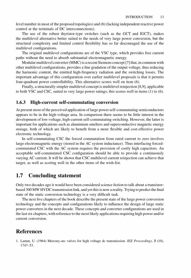
References
1. Lamm, U. (1964) Mercury-arc valves for high voltage dc transmission. IEE Proceedings, 3 (10),
1747–53.
INTRODUCTION 13
2. Lips, H.P. (1997) Semiconductor power devices for use inHVdc and FACTS controllers. Intemational
Colloquium on HVDC and FACTS, Johannesburg, South Africa, 1997, paper 6.8.
3. Lips,H.P. (1996). Semiconductor power devices for use inHVDCandFACTScontrollers. Conference
Internationale des Grandes Reseaux Working Group (CIGRE WG) 14.17.
4. Shakweh, Y. (1999) New breed of medium voltage converters. IEE Power Engineering Journal,
13 (2), 297–307.
5. CIGRE Study Committee B4-WG 37 (2005) VSC Transmission. CIGRE, Paris.
6. Arrillaga, J., Liu, Y.H. andWatson, N.R. (2007) Flexible Power Transmission – The HVDCOptions.
John Wiley & Sons Ltd, London.
7. Dorn, J., Huang, H. and Retzmann, D. (2007)Novel voltage source converters for HVDC and FACTS
applications. CIGRE Annual Conference, Osaka (Japan), November.
8. Perera, L.B., Liu, Y.H., Watson, N.R. and Arrillaga, J. (2005) Multi-level current reinjection in
double-bridge self-commutated current source conversion. IEEE Transactions on Power Delivery,
20 (2), 984–91.
9. Liu, Y.H., Arrillaga, J. and Watson, N.R. (2004) Multi-level voltage reinjection – a new concept in
high power voltage source conversion. IEEProceedings, Generation, Transmission andDistribution,
151 (3), 290–8.
14 SELF-COMMUTATING CONVERTERS FOR HIGH POWER APPLICATIONS

2
Principles of Self-Commutating
Conversion
2.1 Introduction
The conventional line-commutated large power converters normally use the current source
conversion principle. Both during rectification and inversion they absorb varying quantities
of reactive power in their normal operation and inject substantial harmonic currents into the
AC system. These conditions require complex and expensive converter stations and cause
voltage and harmonic interactions with the AC system to which they are connected. Although
the experience of many years has managed to reduce, if not completely eliminate, these
problems, the extra cost involved is very substantial and the scheme’s reliability is reduced
by the number of components.
The progressive development of the self-commutated conversion techniques permits the
design of high-power converter systems without the need of passive filters and shunt reactive
power compensators; this results in substantial cost reduction and elimination of potential
harmonic interactions between the converter and the power system.
Although the progress already made with self-commutation has been great, we are still
speculating on the extent to which self-commutating based technologies should be developed
to exploit the great potential available in the future.
For power transmission application, the voltage needs to be high to reduce losses and, thus,
to match the high voltage rating the converter valves consist of many series-connected
switches. Similarly, for industry applications requiring very high currents, many switching
devices need to be connected in parallel to match the high current rating.
The dynamic and steady state voltages and currents of these configurations are now well
understood and the design of very large power conversion systems presents no special
problem.
This chapter introduces the principles of self-commutating conversion with emphasis
on VSC, which is at present the preferred option. In later chapters, however, it will be
Self-Commutating Converters for High Power Applications J. Arrillaga, Y. H. Liu, N. R. Watson and N. J. Murray
� 2009 John Wiley & Sons, Ltd
shown that for high-power applications there is considerable potential for a self-commutating
CSC technology.
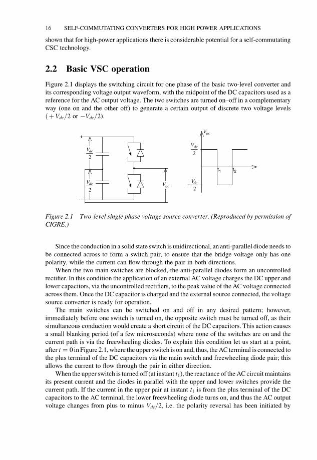
2.2 Basic VSC operation
Figure 2.1 displays the switching circuit for one phase of the basic two-level converter and
its corresponding voltage output waveform, with the midpoint of the DC capacitors used as a
reference for the AC output voltage. The two switches are turned on–off in a complementary
way (one on and the other off) to generate a certain output of discrete two voltage levels
ðþVdc=2 or �Vdc=2).
Since the conduction in a solid state switch is unidirectional, an anti-parallel diode needs to
be connected across to form a switch pair, to ensure that the bridge voltage only has one
polarity, while the current can flow through the pair in both directions.
When the two main switches are blocked, the anti-parallel diodes form an uncontrolled
rectifier. In this condition the application of an external AC voltage charges the DC upper and
lower capacitors, via the uncontrolled rectifiers, to the peak value of the AC voltage connected
across them. Once the DC capacitor is charged and the external source connected, the voltage
source converter is ready for operation.
The main switches can be switched on and off in any desired pattern; however,
immediately before one switch is turned on, the opposite switch must be turned off, as their
simultaneous conduction would create a short circuit of the DC capacitors. This action causes
a small blanking period (of a few microseconds) where none of the switches are on and the
current path is via the freewheeling diodes. To explain this condition let us start at a point,
after t ¼ 0 in Figure 2.1,where the upper switch is on and, thus, theAC terminal is connected to
the plus terminal of the DC capacitors via the main switch and freewheeling diode pair; this
allows the current to flow through the pair in either direction.
When the upper switch is turned off (at instant t1), the reactance of theACcircuitmaintains
its present current and the diodes in parallel with the upper and lower switches provide the
current path. If the current in the upper pair at instant t1 is from the plus terminal of the DC
capacitors to the AC terminal, the lower freewheeling diode turns on, and thus the AC output
voltage changes from plus to minus Vdc=2, i.e. the polarity reversal has been initiated by
acV
2dcV
2dcV
2
Vdc
2dcV−
Vac
t1 t2
+
-
Figure 2.1 Two-level single phase voltage source converter. (Reproduced by permission of
CIGRE.)
16 SELF-COMMUTATING CONVERTERS FOR HIGH POWER APPLICATIONS