Embed Size (px)
DESCRIPTION
A report on wide band antenna.
Citation preview
1
CHAPTER 1
INTRODUCTION
1.1 OVERVIEW
The recent rapid growth in technology and the successful commercial deployment of
wireless communications are significantly affecting our daily lives. The transition
from analog to digital cellular communications, the rise of third- and fourth-
generation radio systems, and the replacement of wired connections with Wi-Fi and
Bluetooth are enabling consumers to access a wide range of information from
anywhere and at any time. As the consumer demand for higher capacity, faster
service, and more secure wireless connections increases, new enhanced technologies
have to find their place in the overcrowded and scarce radio frequency (RF) spectrum.
This is because every radio technology allocates a specific part of the spectrum; for
example, the signals for TVs, radios, cell phones, and so on are sent on different
frequencies to avoid interference to each other. As a result, the constraints on the
availability of the RF spectrum become more and stricter with the introduction of new
radio services. Ultra-wideband (UWB) technology offers a promising solution to the
RF spectrum drought by allowing new services to coexist with current radio systems
with minimal or no interference. This coexistence brings the advantage of avoiding
the expensive spectrum licensing fees that providers of all other radio services must
pay.
In spite of all these advantages, one of the practical problems faced by UWB
systems is the interference due to the coexistence of UWB with several other
narrowband services. For example, IEEE 802.11a which works around 5 GHz band is
a main source of interference to indoor UWB systems. Another example is the effect
of worldwide interoperability for Microwave access (WiMAX) and up link frequency
band for Standard C-band (5.8-6.4 GHz), Extended C-band (6.4-6.7 GHz), and
INSAT/Super Extended C-band (6.7-7.0 GHz), which is used for satellite application,
creates interference to the UWB systems as its operating frequency overlaps with
UWB system band. So, antenna with notch characteristics is enviable when other
services coexist with the UWB.
2
The main aim of this project work is to develop UWB slot antennas to meet all
of the above requirements. In order to achieve these, a UWB antennas and notch
antennas for the rejection of UP link of C-band satellite and WiMAX, bands between
3.1 GHz to 10.6 GHz are developed and presented in this report. Behaviour of UWB
antenna and band notch antenna characteristics such as return loss, radiation pattern
and gain are analysed. The dimensions of the proposed antennas are appropriately
chosen to improve the performance.
1.2 HISTORY AND BACKGROUND
Ultra-wideband communications is fundamentally different from all other
communication techniques because it employs extremely narrow RF pulses to
communicate between transmitters and receivers. Utilizing short-duration pulses as
the building blocks for communications directly generates a very wide bandwidth and
offers several advantages, such as large throughput, covertness, robustness to
jamming, and coexistence with current radio services.
Ultra-wideband communications is not a new technology; in fact, it was first
employed by Guglielmo Marconi in 1901 to transmit Morse code sequences across
the Atlantic Ocean using spark gap radio transmitters. However, the benefit of a large
bandwidth and the capability of implementing multiuser systems provided by
electromagnetic pulses were never considered at that time.
Approximately fifty years after Marconi, modern pulse-based transmission
gained momentum in military applications in the form of impulse radars. Some of the
pioneers of modern UWB communications in the United States from the late 1960s
are Henning Harmuth of Catholic University of America and Gerald Ross and K. W.
Robins of Sperry Rand Corporation [1]. From the 1960s to the 1990s, this technology
was restricted to military and Department of Defence (DOD) applications under
classified programs such as highly secure communications. However, the recent
advancement in microprocessing and fast switching in semiconductor technology has
made UWB ready for commercial applications. Therefore, it is more appropriate to
consider UWB as a new name for a long-existing technology.
As interest in the commercialization of UWB has increased over the past
several years, developers of UWB systems began pressuring the FCC to approve
UWB for commercial use. In February 2002, the FCC approved the First Report and
3
Order (R&O) for commercial use of UWB technology under strict power emission
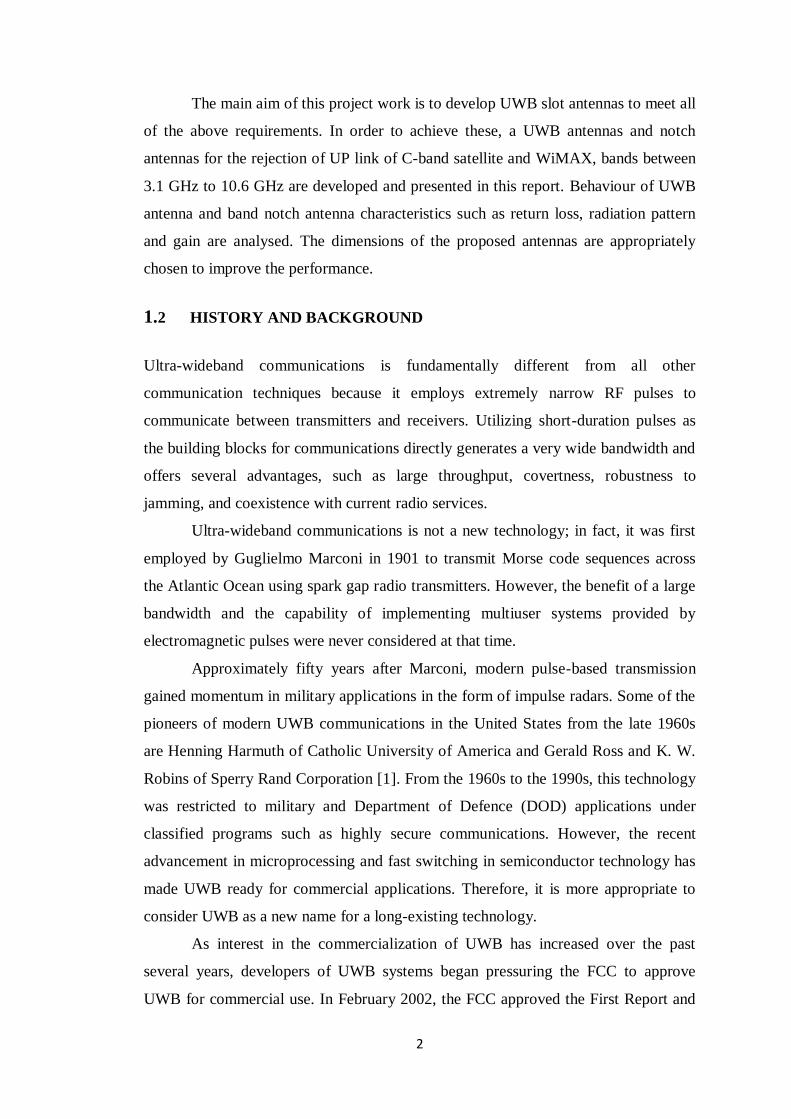
limits for various devices [2]. Figure 1.1 summarizes the development timeline of
UWB.
FCC approves the use Spark Gap Military Radars and of Unlicensed UWB for Transmission, Hertz covert communications commercial purposes and Marconi
1900 1960 1990 2002
standardization
efforts continues...
Figure 1.1: A brief history of UWB developments
1.3 FEEDING METHODS
There are many methods of feeding a Microstrip antenna. These methods can be
classified into two categories-
a) Contacting.
b) Non-contacting.
In the contacting method, the RF power is fed directly to the radiating patch using a
connecting element such as a microstrip line/Coaxial Cable.
In the non-contacting scheme, electromagnetic field coupling is done to
transfer power between the microstrip line and the radiating patch such as aperture
coupling and proximity coupling [3].
.
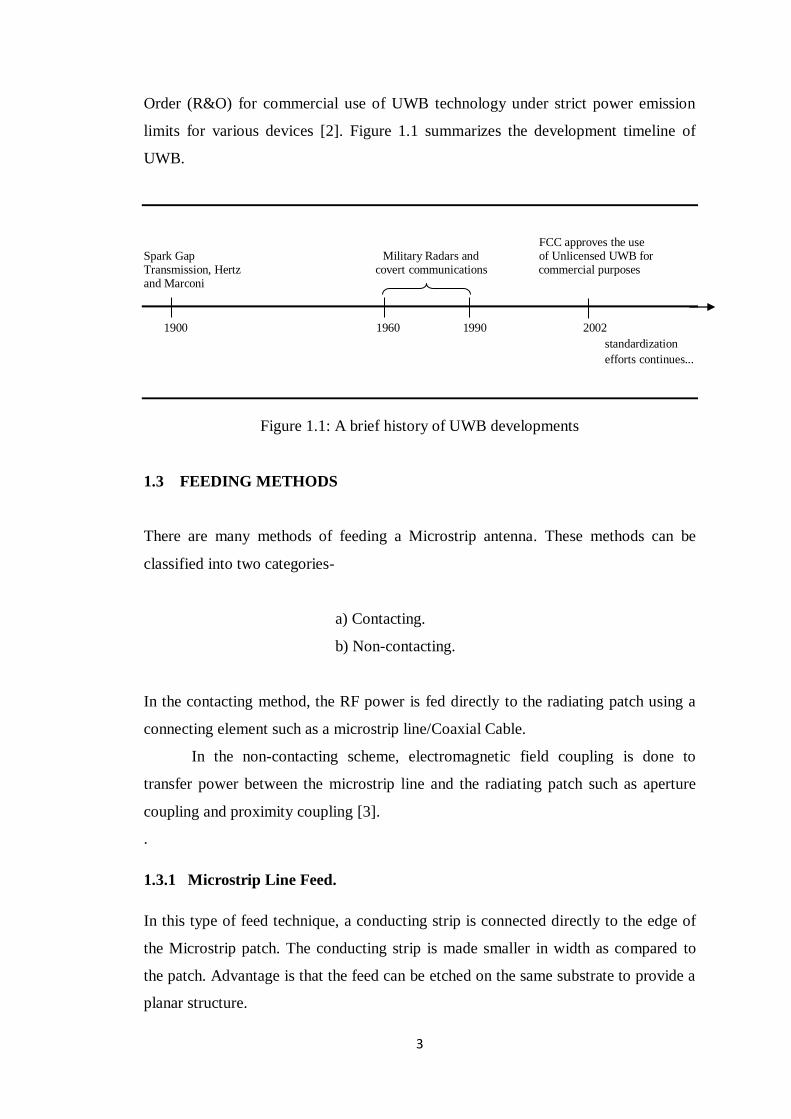
1.3.1 Microstrip Line Feed.
In this type of feed technique, a conducting strip is connected directly to the edge of
the Microstrip patch. The conducting strip is made smaller in width as compared to
the patch. Advantage is that the feed can be etched on the same substrate to provide a
planar structure.
4
Figure 1.2: Microstrip line feed
Actually this kind of feeding has very high resonant input impedance. The
Resonant input impedance can be decreased by using an inset feed recessed by some
distance from the input slot. Impedance matching leads to less reflection loss at the
feed-slot junction. However, the inset feed introduces a physical notch and this notch
introduces junction capacitance and this junction can affect the resonant frequency.
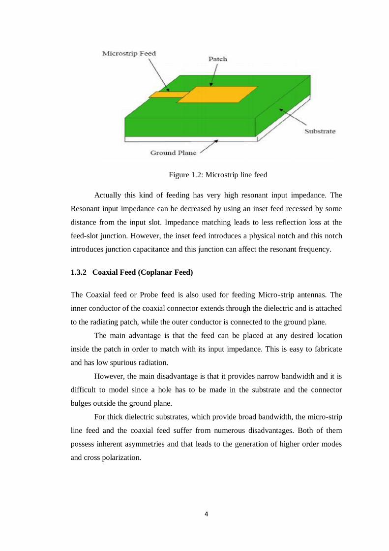
1.3.2 Coaxial Feed (Coplanar Feed)
The Coaxial feed or Probe feed is also used for feeding Micro-strip antennas. The
inner conductor of the coaxial connector extends through the dielectric and is attached
to the radiating patch, while the outer conductor is connected to the ground plane.
The main advantage is that the feed can be placed at any desired location
inside the patch in order to match with its input impedance. This is easy to fabricate
and has low spurious radiation.
However, the main disadvantage is that it provides narrow bandwidth and it is
difficult to model since a hole has to be made in the substrate and the connector
bulges outside the ground plane.
For thick dielectric substrates, which provide broad bandwidth, the micro-strip
line feed and the coaxial feed suffer from numerous disadvantages. Both of them
possess inherent asymmetries and that leads to the generation of higher order modes
and cross polarization.
5
Figure 1.3: Probe fed Rectangular Micro-strip Patch Antenna.
The non-contacting feed methods can solve the problems faced by contacting
feed methods.
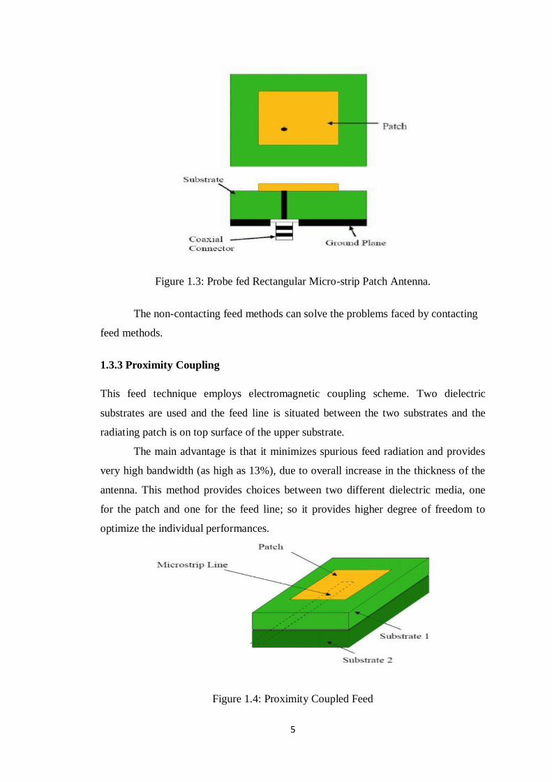
1.3.3 Proximity Coupling
This feed technique employs electromagnetic coupling scheme. Two dielectric
substrates are used and the feed line is situated between the two substrates and the
radiating patch is on top surface of the upper substrate.
The main advantage is that it minimizes spurious feed radiation and provides
very high bandwidth (as high as 13%), due to overall increase in the thickness of the
antenna. This method provides choices between two different dielectric media, one
for the patch and one for the feed line; so it provides higher degree of freedom to
optimize the individual performances.
Figure 1.4: Proximity Coupled Feed
6
The major disadvantage of this feeding method is that it is difficult to manufacture
because of the two dielectric layers which need proper alignment. Also, there is an
increase in the overall thickness of the microstrip antenna.
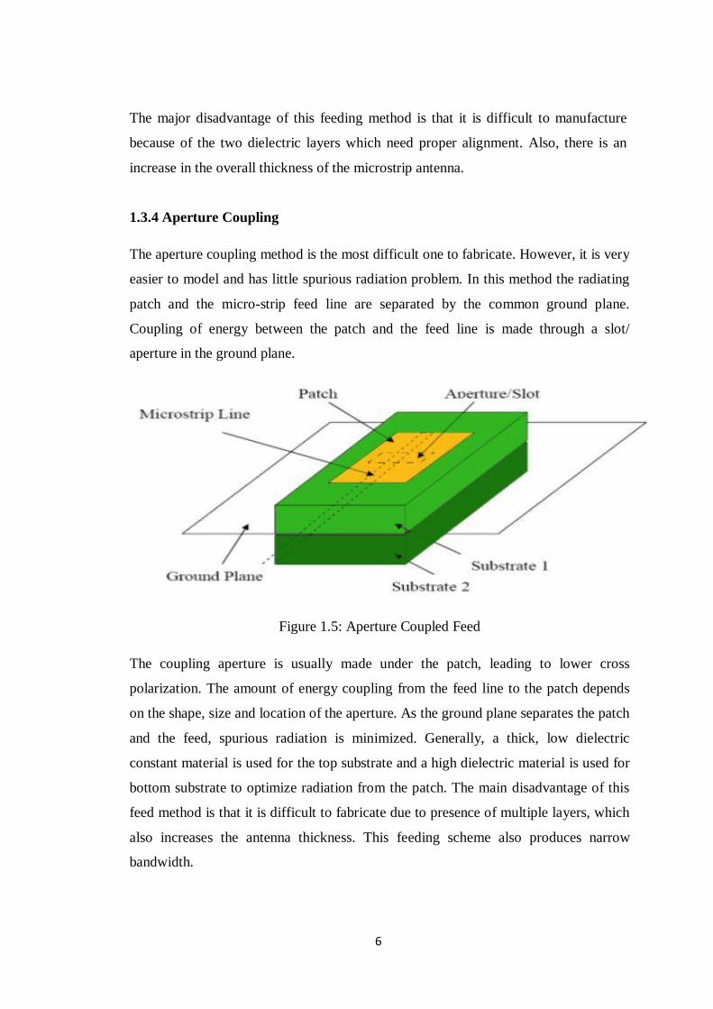
1.3.4 Aperture Coupling
The aperture coupling method is the most difficult one to fabricate. However, it is very
easier to model and has little spurious radiation problem. In this method the radiating
patch and the micro-strip feed line are separated by the common ground plane.
Coupling of energy between the patch and the feed line is made through a slot/
aperture in the ground plane.
Figure 1.5: Aperture Coupled Feed
The coupling aperture is usually made under the patch, leading to lower cross
polarization. The amount of energy coupling from the feed line to the patch depends
on the shape, size and location of the aperture. As the ground plane separates the patch
and the feed, spurious radiation is minimized. Generally, a thick, low dielectric
constant material is used for the top substrate and a high dielectric material is used for
bottom substrate to optimize radiation from the patch. The main disadvantage of this
feed method is that it is difficult to fabricate due to presence of multiple layers, which
also increases the antenna thickness. This feeding scheme also produces narrow
bandwidth.
7
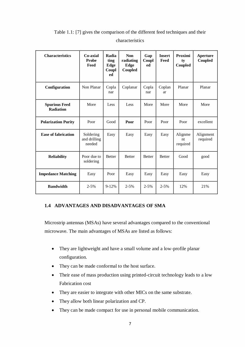
Table 1.1: [7] gives the comparison of the different feed techniques and their
characteristics
Characteristics Co-axial
Probe
Feed
Radia
ting
Edge
Coupl
ed
Non
radiating
Edge
Coupled
Gap
Coupl
ed
Insert
Feed
Proximi
ty
Coupled
Aperture
Coupled
Configuration Non Planar Copla
nar
Coplanar Copla
nar
Coplan
ar
Planar Planar
Spurious Feed
Radiation
More Less Less More More More More
Polarization Purity Poor Good Poor Poor Poor Poor excellent
Ease of fabrication Soldering
and drilling
needed
Easy Easy Easy Easy Alignme
nt
required
Alignment
required
Reliability Poor due to
soldering
Better Better Better Better Good good
Impedance Matching Easy Poor Easy Easy Easy Easy Easy
Bandwidth 2-5% 9-12% 2-5% 2-5% 2-5% 12% 21%
1.4 ADVANTAGES AND DISADVANTAGES OF SMA
Microstrip antennas (MSAs) have several advantages compared to the conventional
microwave. The main advantages of MSAs are listed as follows:
They are lightweight and have a small volume and a low-profile planar
configuration.
They can be made conformal to the host surface.
Their ease of mass production using printed-circuit technology leads to a low
Fabrication cost
They are easier to integrate with other MICs on the same substrate.
They allow both linear polarization and CP.
They can be made compact for use in personal mobile communication.
8
Disadvantages
MSAs suffer from some disadvantages as compared to conventional microwave
antennas. They are the following:
Narrow bandwidth.
Spurious radiation (surface waves).
Need quality substrates (tanδ<0.002)
Difficult to achieve polarization purity.
Lower Power handling capability.
Large ohmic loss in the feed structures.
High Q-factor (sometimes more than 100).
Low Efficiency.
To overcome the problem of Microstrip antennas, we use CPW feeding
technique. In particular, CPW fed antennas have many salient features like less
radiation loss, less dispersion, easy integration with monolithic microwave integrated
circuits (MMIC). Therefore, CPW fed slot antennas are currently under consideration
for use of UWB systems for the numerous applications such as remote sensing, radar,
imaging, localization and medical applications.
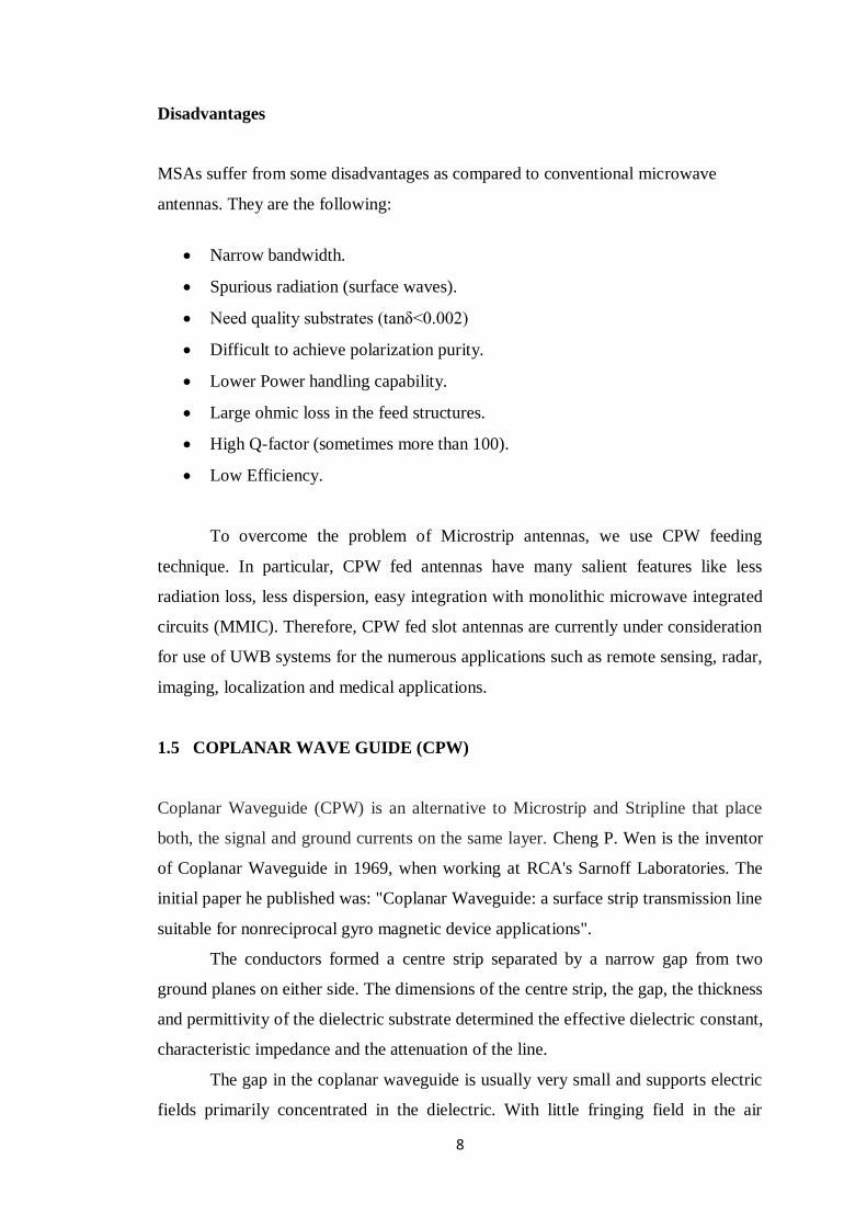
1.5 COPLANAR WAVE GUIDE (CPW)
Coplanar Waveguide (CPW) is an alternative to Microstrip and Stripline that place
both, the signal and ground currents on the same layer. Cheng P. Wen is the inventor
of Coplanar Waveguide in 1969, when working at RCA's Sarnoff Laboratories. The
initial paper he published was: "Coplanar Waveguide: a surface strip transmission line
suitable for nonreciprocal gyro magnetic device applications".
The conductors formed a centre strip separated by a narrow gap from two
ground planes on either side. The dimensions of the centre strip, the gap, the thickness
and permittivity of the dielectric substrate determined the effective dielectric constant,
characteristic impedance and the attenuation of the line.
The gap in the coplanar waveguide is usually very small and supports electric
fields primarily concentrated in the dielectric. With little fringing field in the air
9
space, the coplanar waveguide exhibits low dispersion. In order to concentrate the
fields in the substrate area and to minimize radiation, the dielectric substrate thickness
is usually set equal to about twice the gap width.
CPW has a zero cut-off frequency (suitable for wideband), but its low order
propagation mode is indicated with Quasi-TEM because it is not a real TEM
mode. At higher frequencies, the field becomes less-TEM, and more TE in nature.
The CPW magnetic field is elliptically polarized. CPW it is a printed circuit analogs
of the three-wire transmission lines.
-
Figure 1.6: Coplanar Wave Guide
Figure 1.7: Field Distribution of CPW
Like stripline, CPW has two ground planes, which must be maintained at the
same potential to prevent unwanted modes of propagating. If the grounds are at
different potentials, the CPW mode will become uneven, with a higher field in one
gap than the other.
In the CPW two fundamental modes are supported: the coplanar mode, and the
parasitic slot line mode. Air bridges between ground planes have to be applied to
10
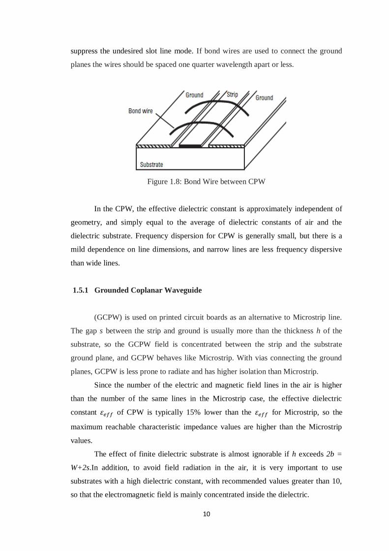
suppress the undesired slot line mode. If bond wires are used to connect the ground
planes the wires should be spaced one quarter wavelength apart or less.
Figure 1.8: Bond Wire between CPW
In the CPW, the effective dielectric constant is approximately independent of
geometry, and simply equal to the average of dielectric constants of air and the
dielectric substrate. Frequency dispersion for CPW is generally small, but there is a
mild dependence on line dimensions, and narrow lines are less frequency dispersive
than wide lines.
1.5.1 Grounded Coplanar Waveguide
(GCPW) is used on printed circuit boards as an alternative to Microstrip line.
The gap s between the strip and ground is usually more than the thickness h of the
substrate, so the GCPW field is concentrated between the strip and the substrate
ground plane, and GCPW behaves like Microstrip. With vias connecting the ground
planes, GCPW is less prone to radiate and has higher isolation than Microstrip.
Since the number of the electric and magnetic field lines in the air is higher
than the number of the same lines in the Microstrip case, the effective dielectric
constant of CPW is typically 15% lower than the for Microstrip, so the
maximum reachable characteristic impedance values are higher than the Microstrip
values.
The effect of finite dielectric substrate is almost ignorable if h exceeds 2b =
W+2s.In addition, to avoid field radiation in the air, it is very important to use
substrates with a high dielectric constant, with recommended values greater than 10,
so that the electromagnetic field is mainly concentrated inside the dielectric.
11
In CPW a ground plane exists between any two adjacent lines, hence cross talk
effects between adjacent lines are very week. As a result, CPW circuits can be made
denser than conventional Microstrip circuits.
1.5.2 Coplanar wave guide and its application in antennas
The coplanar waveguide was invented by C.P. Wen in 1969. Conventional
CPW consists of a centre strip conductor with semi-infinite ground planes on either
side on a dielectric substrate. Compared to a Microstrip line the CPW provides many
advantages like simplicity in fabrication, easy shunt as well as series surface
mounting of active and passive devices, eliminating the need for wraparound and via
holes, and reduction in radiation loss. In addition the ratio of a/b determines the
characteristic impedance so size reduction is possible. Moreover a ground plane exists
between any two adjacent lines; hence cross talk effects between adjacent lines are
very week. Therefore, CPW circuits can be made denser than conventional Microstrip
circuits. These, as well as several other advantages, make CPW ideally suited for MIC
as well as MMIC applications.
1.6 MOTIVATION
The UWB technology has experienced many significant developments in
recent years. However, there are still challengers in making this technology live up to
its full potential. One particular challenge is the UWB antenna.
Among the classical broadband antenna configurations that are under
consideration for use in UWB systems, a straight wire monopole features a simple
structure, but its bandwidth is only around 10%. A Vivaldi antenna is a directional
antenna [4] and hence unsuitable for indoor systems and portable devices. A biconical
antenna has a big size which limits its application. Log periodic and spiral antennas
tend to be dispersive and suffer severe ringing effect, part from big size [5]. There is a
growing demand for small and low cost UWB antennas that can provide satisfactory
performances in both frequency domain and time domain. In recent years, the circular
disc monopole antenna has attracted considerable research interest due to its simple
structure and UWB characteristics with nearly Omni-directional radiation patterns [6].
However, it is still not clear why this type of antenna can achieve ultra-wide
12
bandwidth and how exactly it operates over the entire bandwidth. In this report, a
CPW fed octagonal antenna is investigated in detail in order to understand its
operation, find out the mechanism that leads to the UWB characteristic and also
obtain some quantitative guidelines for designing of this type of antenna.
1.7 OBJECTIVE
The objectives of the research work are,
To develop an inexpensive, light-weight, and portable new type of UWB
antennas for pulsed application
To develop UWB antennas to work without interference from the narrowband
services when they coexist with the UWB service
In order to achieve the above objectives, a comprehensive literature survey is
conducted to identify an appropriate antenna that satisfies the required design
considerations of the UWB antennas.
1.8 SCOPE OF THE PROJECT
The scopes defined for this project are as follows:
Understanding the antenna concept.
Perform numerical solutions using IE3D software
Analysed antenna properties.
1.9 ORGANIZATION OF THESIS
Chapter 1: In the first chapter basic overview of the project done is provided. This
chapter describes the history and background, feeding technique, objectives of the
research work, motivation and organization of the thesis. The remaining chapters of
the thesis are organized as follows:
Chapter 2: In this chapter, presents a relevant theory and literature survey of UWB
antenna and its geometric structures This chapter describes an overview of UWB
13
concepts, fundamentals of UWB technology, primary requirements of UWB antennas,
the advantages and applications, and.
Chapter 3: This chapter presents the developed elemental hexagonal slot UWB
antenna using CPW feeding method. Performance and characteristics of the antennas
are investigated in both frequency and time domains. In addition, Design of UWB
antennas with notch and the important characteristics, which affect the antenna
performance, are investigated.
Chapter 4: This chapter presents simulation results of hexagonal slot containing
octagonal patched UWB antenna and its parametric analysis. Further, developed band
notch Antennas and discusses the important characteristics of single and dual notch
UWB antennas, which affect the antenna performance, are investigated both
numerically and experimentally. The experimentally measured result shows a
reasonably good agreement with simulated one.
Chapter 5: This includes conclusions and future scope to this project work


![A NOVEL ULTRA WIDE BAND YAGI MICROSTRIP ANTENNA · PDF fileA NOVEL ULTRA WIDE BAND YAGI MICROSTRIP ANTENNA FOR WIRELESS APPLICATIONS ... [14] HFSS: High frequency structure simulator](https://img.pdfslide.us/doc/110x75/5a7034b87f8b9abb538bb8bd/a-novel-ultra-wide-band-yagi-microstrip-antenna-wwwjatitorgvolumesresearch-papersvol22no14vol22no1pdfpdf.jpg)