Embed Size (px)
Citation preview

Page 1157
Reducing Energy Consumption by Using Data Encoding
Techniques in Network-On-Chip
V.Ravi Kishore Reddy
M.Tech Student,
Department of ECE
Vijaya Engineering College,
Ammapalem, Thanikella (m),
Khammam, Telangana State.
N.Veeraiah Chowdary
Associate Professor
Department of ECE
Vijaya Engineering College,
Ammapalem, Thanikella (m),
Khammam, Telangana State.
Ayesha Tarannum
Associate Professor & HoD
Department of ECE
Vijaya Engineering College,
Ammapalem, Thanikella (m),
Khammam, Telangana State.
Abstract
As technology shrinks, the power dissipated by the
links of a network-on-chip (NoC) starts to compete
with the power dissipated by the other elements of the
communication subsystem, namely, the routers and
the network interfaces (NIs). In this paper, we
present a set of data encoding schemes aimed at
reducing the power dissipated by the links of an NoC.
The proposed schemes are general and transparent
with respect to the underlying NoC fabric (i.e., their
application does not require any modification of the
routers and link architecture). Experiments carried
out on both synthetic and real traffic scenarios show
the effectiveness of the proposed schemes, which
allow to save up to 51% of power dissipation and 14%
of energy consumption without any significant
performance degradation and with less than 15%
area overhead in the NI.
Index Terms—Coupling switching activity, data
encoding, interconnection on chip, low power,
network-on-chip (NoC), power analysis.
I. INTRODUCTION
Shifting from a silicon technology node to the next one
results in faster and more power efficient gates but
slower and more power hungry wires [1]. In fact, more
than 50% of the total dynamic power is dissipated in
interconnects in current processors, and this is
expected to rise to 65%–80% over the next several
years [2]. Global interconnect length does not scale
with smaller transistors and local wires. Chip size
remains relatively constant because the chip function
continues to increase and RC delay increases
exponentially. At 32/28 nm, for instance, the RC delay
in a 1-mm global wire at the minimum pitch is 25×
higher than the intrinsic delay of a two-input NAND
fanout of 5 [1].
If the raw computation horsepower seems to be
unlimited, thanks to the ability of instancing more and
more cores in a single silicon die, scalability issues,
due to the need of making efficient and reliable
communication between the increasing number of
cores, become the real problem [3]. The networkon-
chip (NoC) design paradigm [4] is recognized as the
most viable way to tackle with scalability and
variability issues that characterize the Ultra deep sub-
micronmeter era. Nowadays, the on-chip
communication issues are as relevant as, and in some
cases more relevant than, the computation related
issues [4]. In fact, the communication subsystem
increasingly impacts the traditional design objectives,
including cost (i.e., silicon area), performance, power
dissipation, energy consumption, reliability, etc. As
technology shrinks, an ever more significant fraction
of the total power budget of a complex many-core

Page 1158
system-on-chip (SoC) is due to the communication
subsystem.
In this paper, we focus on techniques aimed at
reducing the power dissipated by the network links. In
fact, the power dissipated by the network links is as
relevant as that dissipated by routers and network
interfaces (NIs) and their contribution is expected to
increase as technology scales [5]. In particular, we
present a set of data encoding schemes operating at flit
level and on an end-to-end basis, which allows us to
minimize both the switching activity and the coupling
switching activity on links of the routing paths
traversed by the packets. The proposed encoding
schemes, which are transparent with respect to the
router implementation, are presented and discussed at
both the algorithmic level and the architectural level,
and assessed by means of simulation on synthetic and
real traffic scenarios. The analysis takes into account
several aspects and metrics of the design, including
silicon area, power dissipation, and energy
consumption. The results show that by using the
proposed encoding schemes up to 51% of power and
up to 14% of energy can be saved without any
significant degradation in performance and with 15%
area overhead in the NI.
The rest of this paper is organized as follows. We
briefly discuss related works in Section II, while
Section III presents an overview of the proposed data
encoding schemes. The proposed data encoding
schemes along with possible hardware
implementations and their analysis are described in
Section IV. In Section V, the results for the hardware
overhead, power and energy savings, and performance
reduction of the proposed data encoding schemes are
compared with those of other approaches. Finally, this
paper is concluded in Section VI.
II. RELATED WORKS AND CONTRIBUTIONS
In the next several years, the availability of chips with
1000 cores is foreseen [6]. In these chips, a significant
fraction of the total system power budget is dissipated
by interconnection networks. Therefore, the design of
power-efficient interconnection networks has been the
focus of many works published in the literature dealing
with NoC architectures. These works concentrate on
different components of the interconnection networks
such as routers, NIs, and links. Since the focus of this
paper is on reducing the power dissipated by the links,
in this section, we briefly review some of the works in
the area of link power reduction. These include the
techniques that make use of shielding [7], [8],
increasing line-to-line spacing [9], [10], and repeater
insertion [11]. They all increase the chip area. The data
encoding scheme is another method that was employed
to reduce the link power dissipation. The data
encoding techniques may be classified into two
categories. In the first category, encoding techniques
concentrate on lowering the power due to self-
switching activity of individual bus lines while
ignoring the power dissipation owing to their coupling
switching activity. In this category, bus invert (BI)
[12] and INC-XOR [13] have been proposed for the
case that random data patterns are transmitted via these
lines. On the other hand, gray code [14], T0 [15],
working-zone encoding [16], and T0-XOR [17] were
suggested for the case of correlated data patterns.
Application-specific approaches have also been
proposed [18]–[22].
This category of encoding is not suitable to be applied
in the deep submicronmeter technology nodes where
the coupling capacitance constitutes a major part of the
total interconnect capacitance. This causes the power
consumption due to the coupling switching activity to
become a large fraction of the total link power
consumption, making the aforementioned techniques,
which ignore such contributions, inefficient [23]. The
works in the second category concentrate on reducing
power dissipation through the reduction of the
coupling switching [10], [22]–[30]. Among these
schemes [10], [24]–[28], the switching activity is
reduced using many extra control lines. For example,
the data bus width grows from 32 to 55 in [24]. The
techniques proposed in [29] and [30] have a smaller
number of control lines but the complexity of their
decoding logic is high. The technique described in [29]

Page 1159
is as follows: first, the data are both odd inverted and
even inverted, and then transmission is performed
using the kind of inversion which reduces more the
switching activity. In [30], the coupling switching
activity is reduced up to 39%. In this paper, compared
to [30], we use a simpler decoder while achieving a
higher activity reduction.
Let us now discuss in more detail the works with
which we compare our proposed schemes. In [12], the
number of transitions from 0 to 1 for two consecutive
flits (the flit that just traversed and the one which is
about to traverse the link) is counted. If the number is
larger than half of the link width, the inversion will be
performed to reduce the number of 0 to 1 transitions
when the flit is transferred via the link. This technique
is only concerned about the self-switching without
worrying the coupling switching. Note that the
coupling capacitance in the state-of–the-art silicon
technology is considerably larger (e.g., four times)
compared with the self-capacitance, and hence, should
be considered in any scheme proposed for the link
power reduction.
In addition, the scheme was based on the hop-by-hop
technique, and therefore, encoding/decoding is
performed in each node.
The scheme presented in [26] dealt with reducing the
coupling switching. In this method, a complex encoder
counts the number of Type I (Table I) transitions with
a weighting coefficient of one and the number of Type
II transitions with the weighting coefficient of two. If
the number is larger than half of the link width, the
inversion will be performed. In addition to the
complex encoder, the technique only works on the
patterns whose full inversion leads to the link power
reduction while not considering the patterns whose full
inversions may lead to higher link power consumption.
Therefore, the link power reduction achieved through
this technique is not as large as it could be. This
scheme was also based on the hop-by-hop technique.
In another coding technique presented in [25], bunches
of four bits are encoded with five bits. The encoded
bits were isolated using shielding wires such that the
occurrence of the patterns “101” and “010” were
prevented. This way, no simultaneous Type II
transitions in two adjacent pair bits are induced. This
technique effectively reduces the coupling switching
activity. Although the technique reduces the power
consumption considerably, it increases the data
transfer time, and, hence, the link energy consumption.
This is due to the fact that for each four bits, six bits
are transmitted which increases the communication
traffic. This technique was also based on the hop-by-
hop approach.
A coding technique that reduces the coupling
switching activity by taking the advantage of end-to-
end encoding for wormhole switching has been
presented in [23]. It is based on lowering the coupling
switching activity by eliminating only Type II
transitions.
In this paper, we present three encoding schemes. In
Scheme I, we focus on reducing Type I transitions
while in Scheme II, both Types I and II transitions are
taken into account for deciding between half and full
invert, depending the amount of switching reduction.
Finally, in Scheme III, we consider the fact that Type I
transitions show different behaviors in the case of odd
and even inverts and make the inversion which leads to
the higher power saving.
Page 1160
III.OVERVIEW OF THE PROPOSAL
The basic idea of the proposed approach is encoding
the flits before they are injected into the network with
the goal of minimizing the self-switching activity and
the coupling switching activity in the links traversed
by the flits. In fact, self-switching activity and
coupling switching activity are responsible for link
power dissipation. In this paper, we refer to the end-to-
end scheme. This end-to-end encoding technique takes
advantage of the pipeline nature of the wormhole
switching technique [4]. Note that since the same
sequence of flits passes through all the links of the
routing path, the encoding decision taken at the NI
may provide the same power saving for all the links.
For the proposed scheme, an encoder and a decoder
block are added to the NI. Except for the header flit,
the encoder encodes the outgoing flits of the packet
such that the power dissipated by the inter-router
point-to-point link is minimized [23].
IV. PROPOSED ENCODING SCHEMES
In this section, we present the proposed encoding
scheme whose goal is to reduce power dissipation by
minimizing the coupling transition activities on the
links of the interconnection network. Let us first
describe the power model that contains different
components of power dissipation of a link. The
dynamic power dissipated by the interconnects and
drivers is
P= [ T0→1 (Cs + Cl) + Tc Cc] V𝑑𝑑2 (1)
where T0→1 is the number of 0 → 1 transitions in the
bus in two consecutive transmissions, Tc is the number
of correlated switching between physically adjacent
lines, Cs is the line to substrate capacitance, Cl is the
load capacitance, Cc is the coupling capacitance, Vdd
is the supply voltage, and Fck is the clock frequency.
One can classify four types of coupling transitions as
described in [26]. A Type I transition occurs when one
of the lines switches when the other remains
unchanged. In a Type II transition, one line switches
from low to high while the other makes transition from
high to low. A Type III transition corresponds to the
case where both lines switch simultaneously. Finally,
in a Type IV transition both lines do not change.
The effective switched capacitance varies from type to
type, and hence, the coupling transition activity, Tc, is
a weighted sum of different types of coupling
transition contributions [26]. Therefore
Tc = K1T1 + K2T2 + K3T3 + K4T4 (2)
where Ti is the average number of Type i transition
and Ki is its corresponding weight. According to [26],
we use K1 = 1, K2 = 2, and K3 = K4 = 0. The
occurrence probability of Types I and II for a random
set of data is 1/2 and 1/8, respectively. This leads to a
higher value for K1T 1 compared with K2T 2
suggesting that minimizing the number of Type I
transition may lead to a considerable power reduction.
Using (2), one may express (1) as
P= [ T0→1 (Cs + Cl) + (T1 + T2) Cc] V𝑑𝑑2 FCK (3)
According to [3], Cl can be neglected
P α T0→1 Cs + (T1 + 2T2) Cc (4)
Here, we calculate the occurrence probability for
different types of transitions. Consider that flit (t − 1)
and flit (t) refer to the previous flit which was
transferred via the link and the flit which is about to
pass through the link, respectively. We consider only
two adjacent bits of the physical channel. Sixteen
different combinations of these four bits could occur
(Table I). Note that the first bit is the value of the
generic ith line of the link, whereas the second bit
represents the value of its (i +1)th line. The number of
transitions for Types I, II, III, and IV are 8, 2, 2, and 4,
respectively. For a random set of data, each of these
sixteen transitions has the same probability. Therefore,
the occurrence probability for Types I, II, III, and IV
are 1/2, 1/8, 1/8, and 1/4, respectively. In the rest of
this section, we present three data encoding schemes
designed for reducing the dynamic power dissipation
of the network links along with a possible hardware
implementation of the decoder.
Page 1161
A. Scheme I
In scheme I, we focus on reducing the numbers of
Type I transitions (by converting them to Types III and
IV transitions) and Type II transitions (by converting
them to Type I transition). The scheme compares the
current data with the previous one to decide whether
odd inversion or no inversion of the current data can
lead to the link power reduction.
Power Model:
If the flit is odd inverted before being transmitted, the
dynamic power on the link is
P1 α T0→11
+ (K1T11 + K2T2
1 + K3T31 + K4T4
1)Cc (5)
where T0→11 , T1
1, T21, T3
1 and T41 are the self-
transition activity, and the coupling transition activity
of Types I, II, III, and IV, respectively. Table I reports,
for each transition, the relationship between the
coupling transition activities of the flit when
transmitted as is and when its bits are odd inverted.
Data are organized as follows. The first bit is the value
of the generic ith line of the link, whereas the second
bit represents the value of its (i+1) th line. For each
partition, the first (second) line represents the values at
time t-1(t).
As Table I shows, if the flit is odd inverted, Types II,
III, and IV transitions convert to Type I transitions. In
the case of Type I transitions, the inversion leads to
one of Types II, III, or Type IV transitions. In
particular, the transitions indicated as T1*, T1
**, and
T1*** in the table convert to Types II, III, and IV
transitions, respectively. Also, we have T0→11 =
T0→0(odd) + T0→1(even) where odd/even refers to
odd/even lines. Therefore, (5) can be expressed as
P α (T0→0(odd) + T0→1(even) ) Cs + [K1(T1 + T2+ T3 + T4) +
K2 T1*** + K3 T1
*+ K4 T1**] Cc (6)
Thus, if P > P1, it is convenient to odd invert the flit
before transmission to reduce the link power
dissipation. Using(4) and (6) and noting that Cc/Cs = 4
[26], we obtain the following odd invert condition 1
4T0→1 + T1 + 2T2 >
1
4 (T0→0(odd) + T0→1(even)) + T2 + T3 +
T4 + 2 T1***
Also, since T0→1 = T0→0(odd) + T0→1(even) , one may write 1
4T0→1(odd) + T1 + 2T2 >
1
4 T0→0(odd) + T2 + T3 + T4 + 2
T1*** (7)
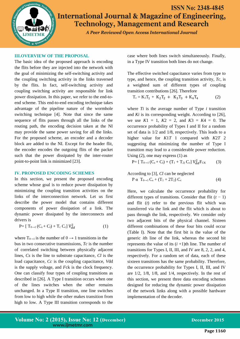
Fig 1: Encoder architecture scheme I. (a) Circuit
diagram [27]. (b) Internal view of the encoder block
(E).
Which is the exact condition to be used to decide
whether the odd invert has to be performed. Since the
terms T0→1(odd) and T0→0(odd) are weighted with a factor
of 1/4, for link widths greater than 16 bits, the
misprediction of the invert condition will not exceed
1.2% on average [23]. Thus, we can approximate the
exact condition as
T1 + 2T2 > T2 + T3 + T4 + 2T1*** (8)
Of course, the use of the approximated odd invert
condition reduces the effectiveness of the encoding
scheme due to the error induced by the approximation
but it simplifies the hardware implementation of
encoder. Now, defining
Tx = T3 + T4 + T1***
and
Ty = T2 + T1 – T1*** (9)
one can rewrite (8) as
Page 1162
Ty > Tx (10)
Assuming the link width of w bits, the total transition
between adjacent lines is w-1, and hence
Ty + Tx = w-1 (11)
Thus, we can write (10) as
Ty > 𝑤−1
2 (12)
This presents the condition used to determine whether
the odd inversion has to be performed or not.
2) Proposed Encoding Architecture:
The proposed encoding architecture, which is based on
the odd invert condition defined by (12), is shown in
Fig. 1. We consider a link width of w bits. If no
encoding is used, the body flits are grouped in w bits
by the NI and are transmitted via the link. In our
approach, one bit of the link is used for the inversion
bit, which indicates if the flit traversing the link has
been inverted or not. More specifically, the NI packs
the body flits in w-1 bits [Fig1(a)].The encoding logic
E, which is integrated into the NI, is responsible for
deciding if the inversion should take place and
performing the inversion if needed. The generic block
diagram shown in Fig. 1(a) is the same for all three
encoding schemes proposed in this paper and only the
block E is different for the schemes. To make the
decision, the previously encoded flit is compared with
the current flit being transmitted. This latter, whose w
bits are the concatenation of w-1 payload bits and a
“0” bit, represents the first input of the encoder, while
the previous encoded flit represents the second input of
the encoder [Fig.1(b)]. The w-1 bits of incoming
(previous encoded) body flit are indicated by Xi(Yi), i
= 0,1,..w-2. The wth bit of the previously encoded
body flit is indicated by inv which shows if it was
inverted (inv = 1) or left as it was (inv = 0). In the
encoding logic, each Ty block takes the two adjacent
bits of the input flits (e.g., X1X2Y1Y2 , X2X3Y2Y3etc.)
and sets its output to “1” if any of the transition types
of Ty is detected. This means that the odd inverting for
this pair of bits leads to the reduction of the link power
dissipation (Table I). The Ty block may be
implemented using a simple circuit. The second stage
of the encoder, which is a majority voter block,
determines if the condition given in (12) is satisfied (a
higher number of 1s in the input of the block compared
to 0s). If this condition is satisfied, in the last stage, the
inversion is performed on odd bits. The decoder circuit
simply inverts the received flit when the inversion bit
is high.
B. Scheme II
In the proposed encoding scheme II, we make use of
both odd (as discussed previously) and full inversion.
The full inversion operation converts Type II
transitions to Type IV transitions. The scheme
compares the current data with the previous one to
decide whether the odd, full, or no inversion of the
current data can give rise to the link power reduction.
Power Model:
Let us indicate with the P,P1,P11 the
power dissipated by the link when the flit is
transmitted with no inversion, odd inversion, and full
inversion, respectively. The odd inversion leads to
power reduction when P1 < P11 and P1 < P. The power
P11 is given by [23]
P'' α T1 + 2T4** (13)
Neglecting the self-switching activity, we obtain the
condition P' < P'' as
T2 + T3 + T4 + 2T1*** < T1 + 2T4
** (14)
Therefore, using (9) and (11), we can write
2(T2 - T4**) < 2 Ty – w + 1 (15)
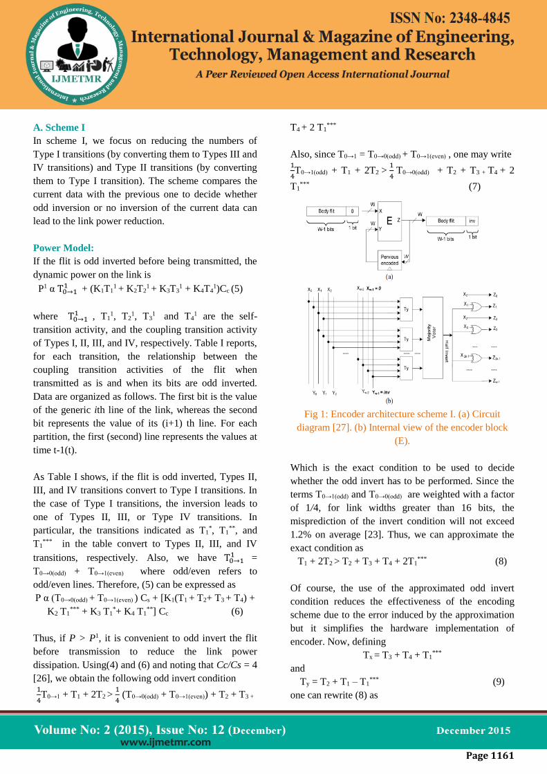
Fig 2: Encoder architecture Scheme II.
Page 1163
Based on (12) and (15), the odd inversion condition is
obtained as
2(T2 – T4**) < 2Ty – w + 1 Ty >
𝑤−1
2 (16)
Similarly, the condition for the full inversion is
obtained from P'' < P and P'' < P'. The inequality P'' < P
is satisfied when
T2 > T4** (17)
Therefore, using (15) and (17), the full inversion
condition is obtained as
2(T2 – T4**) > 2Ty – w + 1 T2 > T4
** (18)
When none of (16) or (18) is satisfied, no inversion
will be performed.
2) Proposed Encoding Architecture:
The operating principles of this encoder are similar to
those of the encoder implementing Scheme I. The
proposed encoding architecture, which is based on the
odd invert condition of (16) and the full invert
condition of (18), is shown in Fig. 2. Here again, the
wth bit of the previously and the full invert condition
of (18) is shown in Fig. 2. Here again, the wth bit of
the previously encoded body flit is indicated with inv
which defines if it was odd or full inverted (inv=1) or
left as it was (inv=0).
In this encoder, in addition to the Ty block in the
Scheme I encoder, we have the T2 and T4** blocks
which determine if the inversion based on the
transition types T2 and T4** should be taken place for
the link power reduction. The second stage is formed
by a set of 1s blocks which count the number of 1s in
their inputs. The output of these blocks has the width
of log2w. The output of the top 1s block determines the
number of transitions that odd inverting of pair bits
leads to the link power reduction. The middle 1s block
identifies the number of transitions whose full
inverting of pair bits leads to the link power reduction.
Finally, the bottom 1s block specifies the number of
transitions whose full inverting of pair bits leads to the
increased link power. Based on the number of 1s for
each transition type, Module A decides if an odd invert
or full invert action should be performed for the power
reduction.
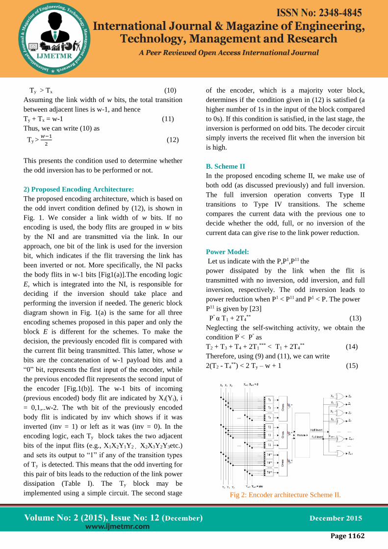
Fig 3: Decoder architecture Scheme II. (a) Circuit
diagram. (b) Internal view of the decoder block (D).
For this module, if (16) or (18) is satisfied, the
corresponding output signal will become “1.” In case
no invert action should be taken place, none of the
output is set to “1.” Module A can be implemented
using full-adder and comparator blocks. The circuit
diagram of the decoder is shown in Fig. 3. The w bits
of the incoming (previous) body flit are indicated by Zi
(Ri) , i = 0,1,..w – 1. The wth bit of the body flit is
indicated by inv which shows if it was inverted (inv =
1) or left as it was (inv = 0). For the decoder, we only
need to have the Ty block to determine which action
has been taken place in the encoder. Based on the
outputs of these blocks, the majority voter block
checks the validity of the inequality given by (12). If
the output is “0” (“1”) and the inv = 1, it means that
half (full) inversion of the bits has been performed.
Using this output and the logical gates, the inversion
action is determined. If two inversion bits were used,
the overhead of the decoder hardware could be
substantially reduced.
Page 1164
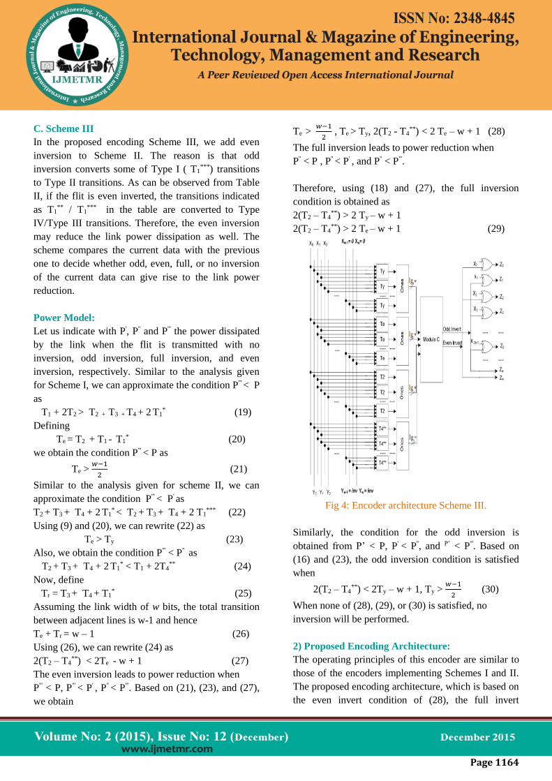
C. Scheme III
In the proposed encoding Scheme III, we add even
inversion to Scheme II. The reason is that odd
inversion converts some of Type I ( T1***) transitions
to Type II transitions. As can be observed from Table
II, if the flit is even inverted, the transitions indicated
as T1** / T1
*** in the table are converted to Type
IV/Type III transitions. Therefore, the even inversion
may reduce the link power dissipation as well. The
scheme compares the current data with the previous
one to decide whether odd, even, full, or no inversion
of the current data can give rise to the link power
reduction.
Power Model:
Let us indicate with P', P'' and P''' the power dissipated
by the link when the flit is transmitted with no
inversion, odd inversion, full inversion, and even
inversion, respectively. Similar to the analysis given
for Scheme I, we can approximate the condition P''' < P
as
T1 + 2T2 > T2 + T3 + T4 + 2 T1* (19)
Defining
Te = T2 + T1 - T1* (20)
we obtain the condition P''' < P as
Te > 𝑤−1
2 (21)
Similar to the analysis given for scheme II, we can
approximate the condition P''' < P' as
T2 + T3 + T4 + 2 T1* < T2 + T3 + T4 + 2 T1
*** (22)
Using (9) and (20), we can rewrite (22) as
Te > Ty (23)
Also, we obtain the condition P''' < P'' as
T2 + T3 + T4 + 2 T1* < T1 + 2T4
** (24)
Now, define
Tr = T3 + T4 + T1* (25)
Assuming the link width of w bits, the total transition
between adjacent lines is w-1 and hence
Te + Tr = w – 1 (26)
Using (26), we can rewrite (24) as
2(T2 – T4**) < 2Te - w + 1 (27)
The even inversion leads to power reduction when
P''' < P, P''' < P' , P'' < P'''. Based on (21), (23), and (27),
we obtain
Te > 𝑤−1
2 , Te > Ty, 2(T2 - T4
**) < 2 Te – w + 1 (28)
The full inversion leads to power reduction when
P'' < P , P'' < P' , and P'' < P'''.
Therefore, using (18) and (27), the full inversion
condition is obtained as
2(T2 – T4**) > 2 Ty – w + 1
2(T2 – T4**) > 2 Te – w + 1 (29)
Fig 4: Encoder architecture Scheme III.
Similarly, the condition for the odd inversion is
obtained from P’ < P, P' < P'', and P’ < P'''. Based on
(16) and (23), the odd inversion condition is satisfied
when
2(T2 – T4**) < 2Ty – w + 1, Ty >
𝑤−1
2 (30)
When none of (28), (29), or (30) is satisfied, no
inversion will be performed.
2) Proposed Encoding Architecture:
The operating principles of this encoder are similar to
those of the encoders implementing Schemes I and II.
The proposed encoding architecture, which is based on
the even invert condition of (28), the full invert
Page 1165
condition of (29), and the odd invert condition of (30),
is shown in Fig. 4. The wth bit of the previously
encoded body flit is indicated by inv which shows if it
was even, odd, or full inverted (inv = 1) or left as it
was (inv = 0). The first stage of the encoder determines
the transition types while the second stage is formed
by a set of 1s blocks which count the number of ones
in their inputs. In the first stage, we have added the Te
blocks which determine if any of the transition types of
T2, T1** , and T1
*** is detected for each pair bits of their
inputs. For these transition types, the even invert
action yields link power reduction.
Again, we have four Ones blocks to determine the
number of detected transitions for each Ty, Te, T2, T4**
, blocks. The output of the Ones blocks are inputs for
Module C. This module determines if odd, even, full,
or no invert action corresponding to the outputs “10,”
“01,” “11,” or “00,” respectively, should be performed.
The outputs “01,” “11,” and “10” show that whether
(28), (29), and (30), respectively, are satisfied. In this
paper, Module C was designed based on the conditions
given in (28), (29), and (30). Similar to the procedure
used to design the decoder for scheme II, the decoder
for scheme III may be designed.
IV.SIMULATION RESULTS
The simulation of the proposed encoding schemes are
carried out by using Modelsim software. The
simulated waveforms and RTL schematics of proposed
schemes are shown in below figures:
Fig 5: Simulation results of Scheme I
Fig 6: Simulation results of Scheme II
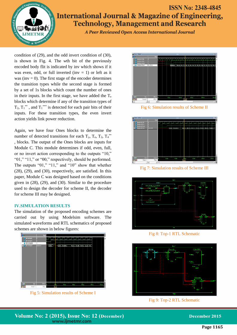
Fig 7: Simulation results of Scheme III
Fig 8: Top-1 RTL Schematic
Fig 9: Top-2 RTL Schematic
Page 1166
Fig 10: Top-3 RTL Schematic
VI. CONCLUSION
In this paper, we have presented a set of new data
encoding schemes aimed at reducing the power
dissipated by the links of an NoC. In fact, links are
responsible for a significant fraction of the overall
power dissipated by the communication system. In
addition, their contribution is expected to increase in
future technology nodes. As compared to the previous
encoding schemes proposed in the literature, the
rationale behind the proposed schemes is to minimize
not only the switching activity, but also (and in
particular) the coupling switching activity which is
mainly responsible for link power dissipation in the
deep sub-micronmeter technology regime. The
proposed encoding schemes are agnostic with respect
to the underlying NoC architecture in the sense that
their application does not require any modification
neither in the routers nor in the links. An extensive
evaluation has been carried out to assess the impact of
the encoder and decoder logic in the NI.
The encoders implementing the proposed schemes
have been assessed in terms of power dissipation and
silicon area. The impacts on the performance, power,
and energy metrics have been studied using a cycle-
and bitaccurate NoC simulator under both synthetic
and real traffic scenarios. Overall, the application of
the proposed encoding schemes allows savings up to
51% of power dissipation and 14% of energy
consumption without any significant performance
degradation and with less than 15% area overhead in
the NI
REFERENCES
[1] International Technology Roadmap for
Semiconductors. (2011) [Online]. Available:
http://www.itrs.net
[2] M. S. Rahaman and M. H. Chowdhury, “Crosstalk
avoidance and errorcorrection coding for coupled
RLC interconnects,” in Proc. IEEE Int. Symp. Circuits
Syst., May 2009, pp. 141–144.
[3] W. Wolf, A. A. Jerraya, and G. Martin,
“Multiprocessor system-on-chip MPSoC technology,”
IEEE Trans. Comput.-Aided Design Integr. Circuits
Syst., vol. 27, no. 10, pp. 1701–1713, Oct. 2008.
[4] L. Benini and G. De Micheli, “Networks on chips:
A new SoC paradigm,” Computer, vol. 35, no. 1, pp.
70–78, Jan. 2002.
[5] S. E. Lee and N. Bagherzadeh, “A variable
frequency link for a poweraware network-on-chip
(NoC),” Integr. VLSI J., vol. 42, no. 4, pp. 479–485,
Sep. 2009.
[6] D. Yeh, L. S. Peh, S. Borkar, J. Darringer, A.
Agarwal, andW. M. Hwu, “Thousand-core chips
roundtable,” IEEE Design Test Comput., vol. 25,
no. 3, pp. 272–278, May–Jun. 2008.
[7] A. Vittal and M. Marek-Sadowska, “Crosstalk
reduction for VLSI,” IEEE Trans. Comput.-Aided
Design Integr. Circuits Syst., vol. 16, no. 3, pp. 290–
298, Mar. 1997.
[8] M. Ghoneima, Y. I. Ismail, M. M. Khellah, J. W.
Tschanz, and V. De, “Formal derivation of optimal
active shielding for low-power on-chip buses,” IEEE
Trans. Comput.-Aided Design Integr. Circuits Syst.,
vol. 25, no. 5, pp. 821–836, May 2006.
[9] L. Macchiarulo, E. Macii, and M. Poncino, “Wire
placement for crosstalk energy minimization in
address buses,” in Proc. Design Autom. Test Eur.
Conf. Exhibit., Mar. 2002, pp. 158–162.

Page 1167
[10] R. Ayoub and A. Orailoglu, “A unified
transformational approach for reductions in fault
vulnerability, power, and crosstalk noise and delay on
processor buses,” in Proc. Design Autom. Conf. Asia
South Pacific, vol. 2. Jan. 2005, pp. 729–734.
AUTHOR DETAILS:
V.Ravi Kishore Reddy has received his B.Tech
degree in Electronics and communication
engineering in 2012 and currently he is pursuing his
M.Tech specialization in EMBEDDED SYSTEMS&
VLSI system design in Vijaya Engineering college.
Sciences which is affiliated to JNTUH, India.
N.Veeraiah Chowdary has received her M.Tech
degree in ECE. Presently he is working as Associate
professor at Vijaya Engineering College, Khammam,
Telangana, India.
Ayesha Tarannum has received her M.Tech degree in
Electronics and communication Engineering. Presently
she has been working at Associate Professor and Head
of ECE Dept.