Embed Size (px)
Citation preview

IDE GuideDocument # 001-42655 Rev **
Cypress Semiconductor198 Champion Court
San Jose, CA 95134-1709Phone (USA): 800.858.1810Phone (Intnl): 408.943.2600
http://www.cypress.com
[+] Feedback

2 PSoC Designer IDE Guide, Document # 001-42655 Rev **
Copyrights
Copyrights
Copyright © 2002-2008 Cypress Semiconductor Corporation. The information contained herein issubject to change without notice. Cypress Semiconductor Corporation assumes no responsibility forthe use of any circuitry other than circuitry embodied in a Cypress product. Nor does it convey orimply any license under patent or other rights. Cypress products are not warranted nor intended tobe used for medical, life support, life saving, critical control or safety applications, unless pursuant toan express written agreement with Cypress. Furthermore, Cypress does not authorize its productsfor use as critical components in life-support systems where a malfunction or failure may reasonablybe expected to result in significant injury to the user. The inclusion of Cypress products in life-sup-port systems application implies that the manufacturer assumes all risk of such use and in doing soindemnifies Cypress against all charges.
PSoC Designer™, Programmable System-on-Chip™, and PSoC Express™ are trademarks andPSoC® is a registered trademark of Cypress Semiconductor Corp. All other trademarks or regis-tered trademarks referenced herein are property of the respective corporations.
Any Source Code (software and/or firmware) is owned by Cypress Semiconductor Corporation(Cypress) and is protected by and subject to worldwide patent protection (United States and for-eign), United States copyright laws and international treaty provisions. Cypress hereby grants to lic-ensee a personal, non-exclusive, non-transferable license to copy, use, modify, create derivativeworks of, and compile the Cypress Source Code and derivative works for the sole purpose of creat-ing custom software and or firmware in support of licensee product to be used only in conjunctionwith a Cypress integrated circuit as specified in the applicable agreement. Any reproduction, modifi-cation, translation, compilation, or representation of this Source Code except as specified above isprohibited without the express written permission of Cypress.
Disclaimer: CYPRESS MAKES NO WARRANTY OF ANY KIND, EXPRESS OR IMPLIED, WITHREGARD TO THIS MATERIAL, INCLUDING, BUT NOT LIMITED TO, THE IMPLIED WARRAN-TIES OF MERCHANTABILITY AND FITNESS FOR A PARTICULAR PURPOSE. Cypress reservesthe right to make changes without further notice to the materials described herein. Cypress does notassume any liability arising out of the application or use of any product or circuit described herein.Cypress does not authorize its products for use as critical components in life-support systems wherea malfunction or failure may reasonably be expected to result in significant injury to the user. Theinclusion of Cypress' product in a life-support systems application implies that the manufacturerassumes all risk of such use and in doing so indemnifies Cypress against all charges.
Use may be limited by and subject to the applicable Cypress software license agreement.
[+] Feedback

PSoC Designer IDE Guide, Document # 001-42655 Rev ** 1
Contents
1. Introduction 71.1 Application Overview ................................................................................................................8
1.1.1 Chip-Level Editor...........................................................................................................81.1.2 System-Level Editor ......................................................................................................91.1.3 Code Editor ...................................................................................................................91.1.4 Build Manager .............................................................................................................101.1.5 Board Monitor..............................................................................................................101.1.6 Debugger ....................................................................................................................111.1.7 Getting Help ................................................................................................................11
1.2 Chapter Overviews .................................................................................................................111.3 Support ...................................................................................................................................12
1.3.1 Technical Support Systems.........................................................................................121.3.2 Product Upgrades .......................................................................................................12
1.4 Conventions............................................................................................................................121.4.1 Acronyms ....................................................................................................................13
1.5 References .............................................................................................................................141.6 Revision History......................................................................................................................14
2. Chip-Level Editor 152.1 Chip-Level Editor Overview ....................................................................................................162.2 Create a Project......................................................................................................................17
2.2.1 Clone a Project............................................................................................................192.2.2 Updating Existing Projects ..........................................................................................19
2.3 Placing User Modules.............................................................................................................192.3.1 Rotating a Placement..................................................................................................212.3.2 Setting User Module Parameters ................................................................................212.3.3 Global Resources........................................................................................................22
2.4 Project Backup Folder ............................................................................................................252.5 Specifying Interconnects.........................................................................................................25
2.5.1 Connecting User Modules...........................................................................................262.5.2 Digital Interconnect Row Input Window ......................................................................322.5.3 Digital Interconnect Row Output Window....................................................................33
2.6 Specifying the Pinout ..............................................................................................................352.6.1 Port Connections.........................................................................................................362.6.2 Port Drive Modes ........................................................................................................402.6.3 Port Interrupts .............................................................................................................41
2.7 Tracking Device Space...........................................................................................................422.8 Design Rule Checker..............................................................................................................432.9 Generating Application Files...................................................................................................442.10 Source Files Generated by Generate Project Operation ........................................................45
2.10.1 About the boot.asm File ..............................................................................................452.11 Configuration Data Sheets......................................................................................................462.12 APIs and ISRs ........................................................................................................................46
[+] Feedback

2 PSoC Designer IDE Guide, Document # 001-42655 Rev **
Copyrights
2.12.1 Working with ISRs ......................................................................................................472.12.2 Interrupt Vectors and the Chip-Level Editor ................................................................48
2.13 Dynamic Reconfiguration .......................................................................................................502.13.1 Adding Configurations ................................................................................................502.13.2 Deleting Configurations ..............................................................................................512.13.3 Renaming Configurations ...........................................................................................522.13.4 Employing Dynamic Reconfiguration..........................................................................52
2.13.4.1 Global Parameters ......................................................................................522.13.4.2 Port Pin Settings..........................................................................................522.13.4.3 Code Editor .................................................................................................532.13.4.4 Code Generation.........................................................................................532.13.4.5 PSoCDynamic Files ....................................................................................552.13.4.6 Active Configurations Display......................................................................552.13.4.7 IO Register Labels.......................................................................................552.13.4.8 Limitations ...................................................................................................55
3. System-Level Editor 573.1 System-Level Editor Overview ...............................................................................................583.2 Create a New Project .............................................................................................................59
3.2.1 Add Design Elements .................................................................................................593.2.2 Use Pop Up Menus.....................................................................................................603.2.3 Use Navigation Tools ..................................................................................................613.2.4 Use the Design Toolbar ..............................................................................................61
3.2.4.1 Select Multiple Elements .............................................................................613.2.4.2 Move Multiple Elements ..............................................................................613.2.4.3 Duplicate Elements .....................................................................................613.2.4.4 Create a Text Label.....................................................................................613.2.4.5 Create a Box ...............................................................................................61
3.2.5 Delete Elements..........................................................................................................623.2.6 Save a Design ............................................................................................................62
3.3 Simulating Your Design ..........................................................................................................623.3.1 Widgets .......................................................................................................................623.3.2 Navigation Tools .........................................................................................................623.3.3 LOG.csv File ...............................................................................................................633.3.4 Simulation Controls.....................................................................................................63
3.4 Drivers ....................................................................................................................................633.4.1 Driver Types................................................................................................................63
3.4.1.1 Input Driver..................................................................................................633.4.1.2 Output Driver ...............................................................................................633.4.1.3 Input/Output Driver ......................................................................................643.4.1.4 Interface Driver............................................................................................64
3.5 Valuators ................................................................................................................................643.5.1 Interface Valuator........................................................................................................643.5.2 Transfer Function Valuator..........................................................................................64
3.6 Transfer Functions..................................................................................................................653.6.1 Transfer Function Types .............................................................................................65
[+] Feedback

PSoC Designer IDE Guide, Document # 001-42655 Rev ** 3
3.6.1.1 LoopDelay ...................................................................................................653.6.1.2 SetPointRegion............................................................................................653.6.1.3 StateMachine...............................................................................................653.6.1.4 PriorityEncoder ............................................................................................663.6.1.5 StatusEncoder .............................................................................................663.6.1.6 TableLookup................................................................................................663.6.1.7 LiteralCode ..................................................................................................66
3.7 Authoring New Design Elements ............................................................................................673.8 Selecting a Configuration........................................................................................................68
3.8.1 Configuration Properties .............................................................................................683.8.2 BOM Vendor................................................................................................................693.8.3 Assign Pins Automatically ...........................................................................................69
3.9 Assigning Pins ........................................................................................................................693.9.1 Pin Color Legend ........................................................................................................703.9.2 Lock Pins.....................................................................................................................703.9.3 Unassign All Pins ........................................................................................................703.9.4 Auto Assign .................................................................................................................70
3.10 Generating Output ..................................................................................................................703.11 Developing Complex Designs.................................................................................................71
3.11.1 Preparing Your Design ................................................................................................713.12 Programming PSoC Flash Memory ........................................................................................763.13 Monitoring Your Design ..........................................................................................................77
3.13.1 Monitoring Your Board With the I2C-USB Bridge........................................................783.13.2 Monitoring Your Board with Other Interfaces ..............................................................80
3.14 Tuning Your Design ................................................................................................................80
4. Code Editor 854.1 File Definitions and Recommendations .................................................................................85
4.1.1 File Types and Extensions ..........................................................................................864.1.2 Project File System .....................................................................................................874.1.3 boot.asm .....................................................................................................................884.1.4 main.asm/main.c .........................................................................................................884.1.5 PSoCConfig.asm.........................................................................................................884.1.6 Additional Generated Files..........................................................................................88
4.2 Working in Code Editor...........................................................................................................904.2.1 Modifying Files ............................................................................................................904.2.2 Adding New Files ........................................................................................................914.2.3 Adding Existing Files...................................................................................................914.2.4 Removing Files ...........................................................................................................914.2.5 Searching Files ...........................................................................................................92
5. Assembler 935.1 Accessing the Assembler .......................................................................................................935.2 The M8C Microprocessor (MCU)............................................................................................93
5.2.1 Address Spaces ..........................................................................................................945.2.2 Instruction Format .......................................................................................................945.2.3 Addressing Modes ......................................................................................................945.2.4 Destination of Instruction Results................................................................................95
5.3 Assembly File Syntax .............................................................................................................955.4 List File Format .......................................................................................................................955.5 Assembler Directives ..............................................................................................................965.6 Instruction Set ........................................................................................................................975.7 Compile and Assemble Files ..................................................................................................97
[+] Feedback

4 PSoC Designer IDE Guide, Document # 001-42655 Rev **
Copyrights
5.8 Calling Assembly Functions From C ......................................................................................98
6. Build Manager 1016.1 Building a Project..................................................................................................................1016.2 C Compiler............................................................................................................................1026.3 Linker....................................................................................................................................102
6.3.1 Customizing Linker Actions ......................................................................................1036.4 Librarian................................................................................................................................103
7. Debugger 1057.1 Debugger Components ........................................................................................................1057.2 Menu Options .......................................................................................................................1067.3 Connecting to the ICE ..........................................................................................................1077.4 Downloading to the Pod .......................................................................................................1087.5 Debug Strategies..................................................................................................................109
7.5.1 Trace......................................................................................................................... 1107.5.2 Break Points.............................................................................................................. 1117.5.3 CPU and Register Views .......................................................................................... 1127.5.4 Watch Variables ........................................................................................................ 113
7.5.4.1 Array Types Added to Global and Local Watch Variables ........................1137.5.5 Dynamic Event Points............................................................................................... 114
7.5.5.1 Configuring Events ....................................................................................1147.5.5.2 Typical Event Uses....................................................................................1157.5.5.3 Event Examples ........................................................................................116
7.5.6 End Point Data.......................................................................................................... 1187.6 Programming the Part ..........................................................................................................119
8. Flash Protection 1218.1 FPMP and PSoC Designer...................................................................................................1218.2 About flashsecurity.txt ..........................................................................................................1228.3 FPMP File Errors ..................................................................................................................123
A. Troubleshooting 125Troubleshooting the Chip-Level Editor ..........................................................................................125Troubleshooting the Code Editor ...................................................................................................126Troubleshooting the Debugger ......................................................................................................127ICE Configuration ..........................................................................................................................127Incorrect Code Compilation ...........................................................................................................127I2C Hot Swapping ..........................................................................................................................128Manually Turning off the Analog Section ......................................................................................128Trace Issues ..................................................................................................................................128Using an External USB Hub ..........................................................................................................129POD Detection Problem ................................................................................................................129Project Cloning Warnings ..............................................................................................................130AreaName Not Defined ..................................................................................................................130General Troubleshooting Issues ....................................................................................................130
B. Build Process 133Build Utilities 133Make Process 134Moving the Build System to Another PC 138Examples 139
[+] Feedback

PSoC Designer IDE Guide, Document # 001-42655 Rev ** 7
1. Introduction
PSoC Designer™ is two tools in one. It combines a full featured integrated development environ-ment (IDE) (the Chip-Level Editor) with a powerful visual programming interface (the System-LevelEditor). The two tools require and support two different design processes:
In the Chip-Level Editor you specify exactly how you want the device configured. This allows youdirect access to all of the features of your PSoC device and complete control over the routing, sys-tem resource use, and firmware development:1. Choose a base device to work with.2. Choose user modules that configure the PSoC device for the functionality you need in your sys-
tem.3. Configure the user modules for your chosen application and connect them to each other and to
the proper pins.4. Generate your project. This prepopulates your project with APIs and libraries that you can use to
program your application.5. Program in C for rapid development, assembly language to get every last drop of performance, or
a combination of both.
In the System-Level Editor you solve design problems the same way you might think about the sys-tem:1. Select input and output devices based upon system requirements.2. Add a communication interface and define the interface to the system (registers).3. Define when and how an output device changes state based upon any/all other system devices.4. Based upon the design, automatically select one or more PSoC Mixed-Signal Controllers that
match system requirements.5. PSoC Designer completely and correctly generates all embedded code, then compiles and links
it into a programming file for a specific PSoC device.6. You can then open the project in Interconnect view to review and further configure your design.
All views of the project share a common code editor, builder, and common debug, emulation, andprogramming tools. The System-Level Editor creates a special environment that allows the visualinterface to function. This special environment is not created if you choose a Chip-level Project. Youcan start with a system-level project and switch to the chip-level view, but the converse is not true.
[+] Feedback

8 PSoC Designer IDE Guide, Document # 001-42655 Rev **
Introduction
1.1 Application OverviewPSoC Designer contains several subsystems: Chip-Level Editor, System-Level Editor, Code Editor,Build Manager, Project Manager, Board Monitor, and Debugger. The interface is split into severalactive windows that differ depending upon which subsystem you are in. As you move between sub-systems, different options are enabled or disabled in the toolbar and menus depending upon thefunctionality of your PSoC device.
1.1.1 Chip-Level EditorIf you select the Chip view in the Workspace Explorer, the main view of the project is the Chip-LevelEditor. The Chip-Level Editor contains a diagram of the resources available on the chip you haveselected; the digital, analog, CapSense™, and other block types that are available on the chip youhave selected and the interconnections between them as well as connections to pins. As you placeuser modules, they will occupy the available resources. You can alter the default placement if youwish. You use this window to route inputs and resources to user modules and user module outputsto other user modules or pins. The default window layout contains the Interconnect view, WorkspaceExplorer, User Module Catalog, Global Resources, Properties, and Data Sheet Windows. There arealso a number of other windows available from the View menu that show details of different aspectsof PSoC Designer. You can rearrange the work area to suit your own work style.
Figure 1-1. PSoC Designer Interconnect View
Menus
Data Sheet
Properties
User Module
Workspace Explorer
Chip View
GlobalResources
Catalog
ResourcePlacement
[+] Feedback

PSoC Designer IDE Guide, Document # 001-42655 Rev ** 9
Introduction
1.1.2 System-Level EditorThe PSoC Designer System-Level Editor contains three desktops: Design, Simulation, and Monitor,which are selectable with the four subtabs shown in Figure 1-2. When you select each of the differ-ent tabs, the look and use of the main area changes to accommodate the specifics of that desktop.The default window layout contains the Driver Catalog, Workspace Explorer, Properties, andDatasheet Windows. There are also a number of other windows available from the View menu thatshow details of different aspects of PSoC Designer. You can rearrange the work area to suit yourown work style. These desktops are described in more detail later.
Figure 1-2. PSoC Designer System View
The menus allow you to perform various tasks, including opening new or existing designs, as well assaving, closing, building, and programming designs. Most of these commands are available regard-less of the areas in which you work.
1.1.3 Code EditorThe workspace editor is a full-featured text editor designed for editing C and assembly code in yourproject. You can use the application editor to create and edit application files.The default window lay-out contains the Code Editor and Find Results. There are also a number of other windows available
Menus
Datasheet
Subtabs
Properties
Driver
Workspace Explorer
System View
Catalog
[+] Feedback

10 PSoC Designer IDE Guide, Document # 001-42655 Rev **
Introduction
from the View menu that show details of different aspects of PSoC Designer. You can rearrange thework area to suit your own work style.
Figure 1-3. PSoC Designer Code Editor
1.1.4 Build ManagerThe Build Manager is a largely invisible utility that controls the various portions of the build processincluding the compiler (or compilers), assembler, and linker, and manages the process of buildingyour project and preparing it to download to a target device.
The only visible portions of the Build Manager in the PSoC Designer application are the Build menuand the Build options in the Tools > Options dialog.
1.1.5 Board MonitorThe board monitor allows you to monitor the target board of an Express project. The project musthave an appropriate communication interface driver. The board monitor is capable of displaying thereal time results of driver tuners and interface valuators at intervals from one sample per second to256 samples per second.
Figure 1-4. The Board Monitor Variables Chart
[+] Feedback

PSoC Designer IDE Guide, Document # 001-42655 Rev ** 11
Introduction
1.1.6 DebuggerThe debugger has multiple windows that allow you to interact with and observe the code executionon the target PSoC device. The debugger is tightly integrated with the rest of the IDE, and there is noseparate debugger view. Instead, there are a number of different windows that you can use to moni-tor the status of various parts of your target board while debugging, including the following:
Break PointsMemoryWatch VariablesEventsTraceOutput
1.1.7 Getting HelpThe Help menu contains several different options for obtaining more information about how to usePSoC Designer. The Help -> Help Topics window contains information about how PSoC Designerworks. For additional information, the Help -> Documentation selection opens a window showingall of the PDF documentation available with PSoC Designer, including this IDE Guide.
When you first launch PSoC Designer, the Start Page opens in the main application window. Thisstart page contains panes that help you get started quickly using PSoC Designer.
Recent Projects allows you to open any previous saved project, create a new project, or browse to find projects that are not displayed in Recent Projects.Express Design Catalog allows you to choose among numerous preconfigured PSoC Designer designs. These are fully functioning PSoC Designer designs, many of which can be built and pro-grammed on Cypress Evaluation Boards and Kits to give you full functioned examples.PSoC Shortcuts provides a shortcuts to PSoC resources that you may find helpful.
1.2 Chapter OverviewsThis table briefly describes the contents of each chapter in this guide.
Table 1-1. Chapter Overviews
Chapter DescriptionIntroduction Describes the purpose of this guide, provides an application overview and
descriptions of each chapter, supplies product support and upgrade infor-mation, and lists documentation conventions and references for more infor-mation.
Chip-Level Editor Describes the chip-level editor that allows you to work directly with the resources available on a PSoC device, select and configure user modules, and route inputs, outputs, and other resources to and from them.
System-Level Editor Describes the system-level editor that allows you to create projects for PSoC devices at an abstracted system level, where you to select and con-figure various design elements, such as inputs, outputs, valuators, and interfaces.
Code Editor In this chapter you learn how to create the project code.
[+] Feedback

12 PSoC Designer IDE Guide, Document # 001-42655 Rev **
Introduction
1.3 SupportFree support for PSoC Designer is available online at http://www.cypress.com. Resources includetraining seminars, discussion forums, application notes, PSoC consultants, TightLink technical sup-port email/knowledge base, and application support technicians.
Before using the Cypress support services, know the version of PSoC Designer installed on yoursystem. To quickly determine the version of PSoC Designer, click Help > About PSoC Designer.
1.3.1 Technical Support SystemsEnter a support request into the TightLink Technical Support System with a guaranteed responsetime of four hours or view and participate in discussion threads about a wide variety of PSoC devicetopics at http://www.cypress.com/support/login.cfm.
1.3.2 Product UpgradesCypress provides upgrades and version enhancements for PSoC Designer free of charge. You canorder the upgrades from your distributor on CD-ROM or download them directly from the Cypressweb under Software and Drivers. Also provided are critical updates to system documentation underDesign Support > Design Resources > More Resources or go to http://www.cypress.com.
1.4 ConventionsHere are the conventions used throughout this guide.
Assembler In this chapter you receive high-level guidance on programming assembly language source files for the PSoC device.
Build Manager In this chapter you learn the details of building a project, discover more about the C Compiler as well as the basic, transparent functions of the sys-tem Linker and Loader, and Librarian.
Debugger In this chapter you learn how to download your project to the In-Circuit Emu-lator (ICE), use debug strategies, and program the part.
Flash Protection Flash Program Memory Protection (FPMP) allows you to select one of four protection (or security) modes for each 64-byte block within the Flash, based upon the particular application.
Table 1-2. Documentation Conventions
Convention UsageCourier New Displays file locations and source code:
C:\ …cd\icc\, user entered text
Italics Displays file names and reference documentation:sourcefile.hex
Table 1-1. Chapter Overviews (continued)
Chapter Description
[+] Feedback

PSoC Designer IDE Guide, Document # 001-42655 Rev ** 13
Introduction
1.4.1 AcronymsThese are the acronyms used throughout this guide.
[bracketed, bold] Displays keyboard commands in procedures:[Enter] or [Ctrl] [C]
File > New Project Represents menu paths:File > New Project > Clone
Bold Displays commands, menu paths and selections, and icon names in procedures:Click the Debugger icon, and then click Next.
Text in gray boxes Displays cautions or functionality unique to PSoC Designer or the PSoC device.
Table 1-3. Acronyms
Acronym DescriptionADC analog-to-digital converter
API application programming interface
BOM bill of material
C (refers to the C programming language)
DAC digital-to-analog converter
DRC design rule checker
EPP enhanced parallel port
FPMP Flash program memory protection
grep global regular expression print
ICE in-circuit emulator
IDE integrated development environment
IO input/output
ISR interrupt service routine
MCU microcontroller unit
MHz megahertz
OBM on-board monitor
OHCI open host controller interface
PWM pulse width modulator
RAM random access memory
ROM read only memory
SSC system supervisory call
UART universal asynchronous receiver transmitter
UHCI universal host controller interface
USB universal serial bus
Table 1-2. Documentation Conventions (continued)
Convention Usage
[+] Feedback

14 PSoC Designer IDE Guide, Document # 001-42655 Rev **
Introduction
1.5 ReferencesThis guide is part of a larger documentation suite for the PSoC Designer application. It is meant as areference, not as the complete source of information. For the most up-to-date information, go tohttp://www.cypress.com. The documentation listed here provides more specific information on avariety of topics:
PSoC Designer Help Topics (Online Help)PSoC Designer Base Project Author GuidePSoC Designer Channel Author GuidePSoC Designer Driver Author Guide PSoC Designer Transfer Function Author GuidePSoC Designer Development Kit Getting Started GuidePSoC Programmer GuideVarious PSoC Designer application notes and data sheets
1.6 Revision HistoryTable 1-4. Revision History
RevisionPDF
Creation Date
Origin of
ChangeDescription of Change
** May 27, 2008 FSU Put changes to the original PSoC Designer IDE Guide in a new template and assigned a Spec Number.
[+] Feedback

PSoC Designer IDE Guide, Document # 001-42655 Rev ** 15
2. Chip-Level Editor
The Chip-Level Editor allows you to work directly with the resources available on a PSoC device,select and configure user modules, such as analog to digital converters (ADCs), timers, amplifiers,and others, and route inputs, outputs, and other resources to and from them.Figure 2-1. Chip-Level Editor Desktop
[+] Feedback

16 PSoC Designer IDE Guide, Document # 001-42655 Rev **
Chip-Level Editor
2.1 Chip-Level Editor OverviewThe Chip-Level Editor gives you complete control over Chip-Level Projects resource use, routing,and firmware. You choose a specific chip at the beginning of this process:1. Create a Project
This is the first step in both processes, but after naming your project, the first thing that you do in a Chip-Level Project is select a PSoC device.
2. Select a PSoC DeviceThere are a large number of PSoC devices in the PSoC family with more being added all the time. Some are general purpose devices with varying amounts of general purpose digital and analog resources while others are more specialized with onboard peripherals suited to specific solutions such as wireless, LED control, or capacitive sensing. Consult the Cypress web site for a wide variety of literature and contact information for people that can help you choose the right device for your design.
3. Choose User ModulesPSoC devices have programmable analog and digital blocks that can be configured for a wide variety of uses. User Modules configure these programmable blocks to behave as a specific peripheral, such as an analog to digital converter, a timer, or a pulse width modulator. You choose user modules based on what you need the PSoC device to do for you.
4. Configure the User ModulesEach user module has a set of parameters that allow you to configure it to meet your needs. For example, a CapSense user module must be configured to detect signals coming from capacitive sensing components in a wide variety of configurations, so it has a large number of configurable parameters. A design rule checker can alert you to potential problems with your design as you work.
5. Connect The User ModulesEach user module will have inputs, outputs, and interrupts that can be routed internally to and from other user modules, and externally to and from pins. The PSoC devices have a very flexible routing system, but resources are limited and it may take some experimentation to find the opti-mal routing and placement for all of the user modules.
6. Generate Your ProjectThis prepopulates your project with APIs and libraries that you can use to program your applica-tion.
7. Write Your ProgramWrite your program in C for rapid development, assembly language to get every last drop of per-formance from the MCU, or a combination of both. You have a choice of third party C compilers and assemblers for PSoC devices.
8. Build and Debug Your ProgramBuild and test your program. Use PSoC Designer in conjunction with one of the PSoC emulators. PSoC Designer has a powerful built in debugger.
9. Program the DeviceCypress has a variety of programmers that you can use to program your production parts.
Your design is now complete. The remainder of this chapter is organized just like the above outlinewith additional details on each of the steps.
[+] Feedback

PSoC Designer IDE Guide, Document # 001-42655 Rev ** 17
Chip-Level Editor
2.2 Create a ProjectIn order to program the desired functionality into a PSoC device, you need to first create a projectdirectory in which the files and device configurations reside.1. To start a new project, select New Project from the File menu.
Figure 2-2. New Project Dialog Box
The System-Level Editor creates a special environment that allows it to generate all necessary program code based on the elements and logic in the System-Level Project. If you start with an System-Level Project, you can eventually edit in the Chip-Level Editor. The converse is not true. If you start with a Chip-Level Project, the environment necessary to generate code from System-Level designs is not initiated and System-Level Editor functions are disabled in that project.
2. Choose a name and location for the project. By default, a project is created inside a workspace with the same name as the project, the project is stored in the project directory. If you plan to cre-ate multiple projects in a single workspace (for example, if your project will use multiple PSoC devices), click Create a directory for workspace and supply a name for the first project. When you are finished, click Next.
[+] Feedback

18 PSoC Designer IDE Guide, Document # 001-42655 Rev **
Chip-Level Editor
3. In the Select Project Type dialog box, click View Catalog to access a detailed list of available parts.
Figure 2-3. Create New Project Dialog Box
4. In the Parts Catalog Dialog Box, highlight your part of choice. Tabs at the left and characteristic selections along the top narrow the list of devices. You have several options in this dialog box including layout display, viewing part image, and sorting part selection (by clicking on a chosen column title). Click Select to save your selection and exit the dialog box.
Figure 2-4. Parts Catalog Dialog Box
5. Once you select a part, click C or Assembler, in the Select Project Type dialog box, to designate the language in which you want the system to generate the “main” file.
[+] Feedback
PSoC Designer IDE Guide, Document # 001-42655 Rev ** 19
Chip-Level Editor
6. Click OK. Your workspace directory with folders is created and is listed in the Workspace Explorer. If the Workspace Explorer is not visible, choose Workspace Explorer from the View menu.
2.2.1 Clone a ProjectCloning a project is used when you want to convert an existing project to a different PSoC part. Thepart is referred to as the “base” part.
You can clone an existing project at any point of its existence: before, during, or after device config-uration, assembly-source programming, or project debugging. Cloning copies the existing project butallows you to change the base device. Use the cloning method to move an existing project from onedirectory to another, rather than physically moving the files.
You must use the cloning method to change parts within a part family in the middle of a projectdesign. Refer to the Application Notes on the Cypress web site for assistance.
To clone an existing project:1. From the File menu, select New Project. You can only clone a Chip-Level project. Select Chip-
Level .2. Select a name and location for your new application and click OK.3. In the Clone project box click browse and find the .SOC file of the project you want to clone. 4. Choose whether you want to choose a new base device or not. If you do, select View Catalog to
select a new device. 5. Choose C or assembler for the language of the main file. Click OK.
2.2.2 Updating Existing ProjectsIf you download a newer version of PSoC Designer, you may need to update existing projects cre-ated with an earlier version of PSoC Designer. Most project updates are done automatically; how-ever, some need to be done manually depending upon project specifics. Manual project updates aredescribed at the end of this chapter.
To update a PSoC project for compatibility:1. Open PSoC Designer.2. Access the project to update.
At this point, PSoC Designer checks to see if the project is compatible with the new version of PSoC Designer.
3. If your project needs to be updated, the Old Version window appears with the appropriate mes-sage text. Click Update (or you can update later by selecting Update later...).
4. Once the update is complete, click Finish. Your project is now compatible with the current version of PSoC Designer.
2.3 Placing User ModulesPlacing user modules is the first step (after creating a project) in configuring your target device. Auser module is a preconfigured function that, once placed and programmed, works as a peripheralon the target device.
To place a user module:1. Locate the desired user module in the the user module catalog. Each user module has a user
module data sheet that describes what it is and how to use it. If you do not see the user module data sheet when you click on a user module, select View > Datasheet Window. Right-click on
[+] Feedback

20 PSoC Designer IDE Guide, Document # 001-42655 Rev **
Chip-Level Editor
the user module and select Place. Some user modules have wizards or configuration screens that appear before the user module can be placed. These will differ by user module. The user module will be placed in the first available PSoC block in the Interconnect view. The user module block reference names appear above the currently active blocks. For example, an ADC10 has one digital block used as a counter (CNT) and two analog blocks, one for the ana-log to digital conversion (ADC) and the other for a voltage ramp (RAMP). The name of the user module is separate from these user module block function names. This is because a multiblock user module may have distinct block actions.
2. If you want to use a placement other than the default, click the Next Allowed Placement icon to advance the user module to the next available location (active/anchor identified as green, non-active as blue) or use the faster drag-and-drop capability. Click the target placer (identified as green and blue highlights) and drag-and-drop the user module to a new location. If a user module has multiple blocks, it may be possible to drag individual blocks onto a free block. Repeat this procedure until you have identified the exact location for the user module.The Next Allowed Placement button shows the next possible set of PSoC blocks in which a user module may be placed, regardless of any currently placed user modules. If you cannot place the user module in the highlighted location due to a lack of resources, a Resource Allocation mes-sage flashes in the lower-left corner of PSoC Designer. Placement is not possible if another user module occupies the PSoC block, or if a placed user module is using another resource which the highlighted user module requires.
3. When you identify the location, click the Place User Module icon , or right-click and select Place.Once you place the module, it appears on the device, color-coded, bearing the designated name of the chosen PSoC block. In the Interconnect frame, the inactive target placers (blue highlights) of multi-block user modules are now identified by a group name across the top. Some user modules do not consume visible resources in the interconnect view when they are placed. Examples of this include LCD, I2C Master, I2C Slave and software only user modules.
4. At this time, you can print, save, clear or unplace, and name or rename the placed user module.To print your placement view, right-click anywhere in the Interconnect view and select Print.To save your work, click File > Save project.To clear all user module placements (i.e., remove them from their location on the PSoC blocks), click Interconnect > Clear All Placements. To unplace one particular module, right-click it (in either the Interconnect view or the Workspace Explorer) and select Unplace or click the Unplace User Module icon . This does not remove user modules from PSoC Designer or from your collection. Your unplaced user modules shown in the Workspace Explorer under Interconnect > Loadable Configurations > User Modules.To name or rename user modules, select the user module either in the Workspace Explorer or the Interconnect view, and type a new name in the user module Properties window.
5. Repeat this process (steps 1-4) for all user modules in your design.
For each user module you add, the system updates the data in the Resource Meter with the numberof occupied PSoC blocks, along with estimated RAM and ROM usage for the current set of selecteduser modules. The RAM and ROM numbers grow or shrink depending upon wizard settings andother user module parameter adjustments. If you select a user module that requires more resourcesthan are currently available, PSoC Designer does not allow the selection. If you do not see theDevice Resource Meter go to the View menu and select Resource Meter.
If user modules are already placed, then there are some cases when user module placement failseven if it appears that sufficient PSoC blocks remain unallocated. In such cases, the already placeduser modules are using resources that the selected user module requires.
[+] Feedback

PSoC Designer IDE Guide, Document # 001-42655 Rev ** 21
Chip-Level Editor
There are several user modules that require topology selection (i.e., filters). Right-click on the mod-ule in the Aplication Explorer after it is placed and click User Module Selection Options. Make thetopology choice according to your application.
Some user modules have associated wizards to assist in configuration. To access a wizard, selectthe user module in the Workspace Explorer and then right click the mouse. If a wizard exists, itappears in the menu choices.
To Remove a User Module:
To remove user modules from your collection, select the user module in the Workspace Explorerand press [Delete], or right-click the user module and select Delete. This does not remove usermodules from PSoC Designer, just from your collection.
If you add or remove user modules after generating application files, you need to regenerate theapplication files (as well as reconfigure required settings). For further details, see “Generating Appli-cation Files” on page 44.
2.3.1 Rotating a PlacementIn a group placement of two or more user modules, press the [Space Bar] to rotate and see theplacement options around the anchor block of a multi-block user module.
Select the anchor block by clicking on one of the blocks in which the user module is placed. Nowpress the [Space Bar]. The block your cursor is on becomes the anchor block. As you press the[Space Bar], the remaining required blocks rotate to the options that surround the anchor block.
For optimum placement, you may need to switch anchor blocks as well as drag-and-drop the setaround the interface to view all options.
2.3.2 Setting User Module ParametersSetting User Module Parameters configures the user module to behave the way you want it to andconnects the user module to the external pins and other user modules and resources. You connectto user modules through the output and input parameters of the PSoC blocks. The interconnectionbuses provide interconnection paths between the external pins and to other digital user modules.
Once you place the user module, the parameters are updated with applicable names. When you sin-gle-click a user module, you view its parameters under Properties. If you do not see the Propertieswindow, go to the View menu and select Properties Window. User Module Parameters
To update the User Module Parameters:1. Click each drop-arrow (in parameter value fields) and make your selections.
[+] Feedback

22 PSoC Designer IDE Guide, Document # 001-42655 Rev **
Chip-Level Editor
Some parameters are integer values. Set these values by clicking the up/down arrows, or dou-ble-click the value and type in the value. If you type a value that is out of range, an error message appears in the lower-left corner.
2. Repeat this process for all placed user modules.
2.3.3 Global ResourcesGlobal Resources are hardware settings that determine the underlying operation of the part (for theentire application). For example, the CPU clock designates the clock speed of the M8C.
Note that Global Resource options differ slightly for each device family.
To update and save Global Resources:1. Click each drop-arrow (in parameter value fields) and make your selections.
Some parameters in Global Resources are specified as integer values (such as 24V1 and 24V2). Set these values by clicking the up/down arrows or double-clicking the value and typing over them. If you enter an out of range value, you see a dialog box specifying the acceptable range. Click OK to close the dialog box.
2. The current settings for the Global Resources can be saved as default settings. Right-click on any Global Resource name and select Update Default Values. This action saves all Global Resource settings to the \Preferences directory under the PSoC Designer installation path. Use these settings for any other project by right-clicking any Global Resource name and select-ing Restore Default Values. If no custom default values are saved, then the menu item and the right-click to Restore Default Settings restore the factory default Global Resource Settings.
The Global Resources available in PSoC Designer are shown and described briefly in the followingtable.
Table 2-1. Global Resources Example.
Power Setting [Vdd/SysClock Freq]
This parameter allows you to select the SysClock frequency and nominal operating voltage. Basedupon the SysClock selected, the Internal Main Oscillator (IMO) is set with appropriate calibration set-tings. Since many internal clocks are derived from the SysClock, you see significant device power-consumption savings by lowering the SysClock frequency, if the implemented design permits it.
[+] Feedback

PSoC Designer IDE Guide, Document # 001-42655 Rev ** 23
Chip-Level Editor
CPU_Clock
The CPU_Clock selection allows the selection of the M8C clock speed from 93.75 kHz to 24 MHz.The CPU clock is derived directly from the SysClock. Use an external 32 kHz oscillator and the PLLExt_Lock to improve clock accuracy. A discussion of the main oscillator is contained in the PSoCTechnical Reference Manual.
32K_Select
The 32K_Select parameter allows selection of the internal 32 kHz oscillator or an external crystaloscillator. A complete discussion of the implications of this selection is found in the PSoC TechnicalReference Manual.
PLL_Mode
The PSoC Technical Reference Manual discusses use of the phase-locked loop mode.
Sleep_Timer
The Sleep_Timer parameter selects the timing of the sleep interrupt, if enabled. When the sleepinterrupt is active, and the processor is in a sleep state, it is awakened at the rate specified with thisparameter. The Watchdog Reset, if enabled, occurs after three rollover events in the sleep timer (ifthe Watchdog counter is not reset). A complete discussion of the relation of these two elements isfound in the PSoC Technical Reference Manual.
VC1 and VC2
These resources are clocks that can be chained to provide various internal clock frequencies usedfor digital or analog blocks. A complete discussion of system clocking is found in the PSoC TechnicalReference Manual.
VC3_Source and VC3_Divider
VC3 is a system clock resource similar to the VC1 and VC2 resources. The main difference betweenit and VC1 and VC2 is that VC3 may be chained from one of several clock sources and may not beused as an input clock as flexibly as VC1 and VC2. You cannot use it as a direct input to the analogsection of the PSoC. It can be used as an input to a digital PSoC block and then used to derive aclock that can be used in many more places. For this reason, it is important to evaluate clockingoptions as a PSoC design is being developed. Often, rearranging clock sources according to wherethey are most easily connected solves clocking problems. A complete discussion of system clockingis found in the PSoC Technical Reference Manual.
SysClock_Source and SysClock*2 Disable
These parameters allow you to select the 24 MHz system SysClock from an internal or externalsource. The SysClock*2 Disable parameter allows the internal 48 MHz clock to be shut off. A com-plete discussion of system clocking is found in the PSoC Technical Reference Manual.
Analog Power
This parameter controls the power to the analog section of the PSoC. Power is controlled in threestages: 1. All Analog Blocks Off2. Continuous Time Blocks ON/Switched Capacitor Blocks OFF3. Continuous Time Blocks ON/Switched Capacitor Blocks ON
[+] Feedback

24 PSoC Designer IDE Guide, Document # 001-42655 Rev **
Chip-Level Editor
For each of the two 'ON' cases, select reference drive levels of high, medium, and low to choose thecurrent drive capability for the internal reference buffers. All selections of this parameter, whetherused as a User Module Parameter or this Global Resource, need to agree. This selection affects thetotal power consumption of the PSoC. Each user module using the reference and the opamp blockassociated with it adds slightly to the power consumed by the device. Since the internal reference isused as an integral part of most switched capacitor circuits, the current drive capability has animpact on the speed at which the switched capacitor block operates. In general, higher settings forthis parameter allow switched capacitor circuits to operate at higher clock rates, at the expense ofhigher power consumption. To estimate the current (and power) consumption per opamp block, referto the applicable table in the data sheet for the part: DC Operation Amplifier Specifications (ISOA).
Ref Mux
The Ref Mux source selection is used to control the range and (potential) accuracy of various analogresources. The reference chosen controls the maximum voltage that is input to a switched capacitorcircuit and output from a switched capacitor circuit. Both the analog ground level and the peak-to-peak voltage are selected using this parameter. Values specified with the Ref Mux parameter are inpairs and consist of [AGND level ± full scale]. Keep in mind that selecting Vdd (supply voltage) as areference level couples Vdd changes into the AGND input of internal resources. This directly affectsabsolute accuracy of measurements. Using the internal bandgap reference results in better accu-racy but may not offer an exact Vdd/2 input reference. Choices of ± full-scale values also offer anumber of options. These full-scale values may be based on the PSoC internal references or onexternal input voltages. The ± full scale values present constraints similar to those for AGND interms of Vdd variation and absolute range of input/output. Individual design criteria dictate the bestselection for the AGND and ± full-scale values. Further discussion of the analog reference can befound in the PSoC Technical Reference Manual.
AGNDBypass
A provision is made in some versions of the PSoC device to provide an external AGND bypasscapacitor to reduce the small amounts of switching noise present on the internal AGND. This featureis switched on and off using the AGNDBypass global parameter. Typical values for the externalbypass capacitor are 0.01 μF and should not generally exceed 10 μF. The recommended value is 1μF.
Opamp Bias
Performance of the internal opamps are tailored based upon the application under development byselecting high or low bias conditions for the analog section of the PSoC. Selecting high bias causesthe opamp to consume more current but also increases its bandwidth and switching speed, loweringits output impedance. To estimate the current (and power) consumption per opamp block, includingthe effect from high or low selection of opamp Bias, refer to the applicable table in the data sheet forthe part: DC Operation Amplifier Specifications (ISOA). To estimate the effect on AC opamp param-eters, refer to the applicable AC Operational Amplifier Specifications in the device data sheet.
A_Buf_Power
A_Buf_Power allows the user to select the power level for the analog output buffers of the PSoC.These buffers are used to supply internal analog signals to external pins on the PSoC. Power levelsmay affect the frequency response and current drive capability of the output buffers. Completetables for the AC Analog Output Buffer Specifications and DC Analog Output Buffer Specificationsare contained in the applicable device data sheet.
[+] Feedback
PSoC Designer IDE Guide, Document # 001-42655 Rev ** 25
Chip-Level Editor
SwitchModePump
An integrated switch mode pump circuit is available for operation of the device from very low voltagesources. The pump requires a few external components and can be configured to automatically turnon as supply voltage drops. Further discussion of the switch mode pump is found in the PSoC Tech-nical Reference Manual.
Trip Voltage [LVD (SMP)]
A precision POR circuit is integrated into the PSoC. This parameter allows the user to select voltagelevels that the PSoC uses to internally monitor its supply voltage. Two levels are specified in theparameter with the syntax <LVD (SMP)>. LVD is the value at which the internal low voltage compar-ator asserts its control signal. SMP is the level at which the integrated switch mode pump is enabled.Although selection of SMP is implicit in the selection of LVD, if no switch mode pump circuitry isused, the part is reset if supply voltage falls too low. At the point when the supply voltage exceedsthe threshold level, the part resumes operation as if the power was switched off and on (POR). Fur-ther discussion of the switch mode pump and low voltage detect is found in the PSoC Technical Ref-erence Manual.
LVD ThrottleBack
This parameter allows you to configure the PSoC to lower its own CPU clock speed under low volt-age conditions. Use of this parameter and the bit it controls is discussed in the PSoC Technical Ref-erence Manual. Not all PSoC devices incorporate this parameter and bit.
Watchdog Enable
This parameter activates the Watchdog Timer. The Watchdog Timer is based on a counter thatcounts three sleep timer events. To prevent system reset, you must clear this counter before threesleep timer state events occur, or the PSoC is internally reset. The duration of each sleep timerevent is selected using the Sleep_Timer parameter in the Global Resources frame of PSoCDesigner. A complete discussion of the relation of the sleep and watchdog timers is in the PSoCTechnical Reference Manual.
2.4 Project Backup FolderPSoC Designer maintains a backup folder in the project directory for files that were removed fromthe source tree. This includes files that are manually removed and files removed due to cloning orcode generation. The backup folder only retains the version of the file that was last removed. Thefiles are named identically to the original project file and the \lib directory is not retained (i.e.,library files are placed directly under the backup folder).
2.5 Specifying InterconnectsInterconnectivity allows communication between user modules, PSoC blocks, pins, and other on-chip resources.
Connections are shown as lines between elements, special symbols, or flag connectors. Flag con-nectors are used when the connection is made to a point where drawing a line results in a cluttereddisplay, with the legend indicating the origin of the connection. Connections to pins are shown aslines from interconnection buses. The interconnection bus structure depends on the PSoC deviceselected and can consist of one or more levels of buses between the digital PSoC blocks and thepins.
[+] Feedback

26 PSoC Designer IDE Guide, Document # 001-42655 Rev **
Chip-Level Editor
Connections between analog PSoC blocks and pins are made through the analog input muxes andoutput buses.
Pin names are duplicated in several places, since they are multifunctional, and are highlighted whenused with lines showing their current connection state. The location of the pin to which a line isdrawn indicates the usage of the pin. Lines drawn to the pins on the left edge indicate that the pinsare used as inputs, while the right edge indicates the pins are used as output.
Pins in the upper groups indicate connection to the digital network, while lower groups indicate ana-log connections. Lines drawn from multiple locations on the same pin indicate that the shown combi-nation is electrically valid.
To specify interconnections, click the Interconnect folder in the Workspace Explorer.
User module interconnections consist of connections to surrounding PSoC blocks, output bus, inputbus, internal system clocks and references, external pins, and analog output buffers. Multiplexersmay also be configured to route signals throughout the PSoC block architecture.
Digital PSoC blocks are connected through the Global_IN and Global_OUT buses to external pinsand to other digital PSoC blocks. There are eight Global_IN and eight Global_OUT bus lines, num-bered 0 through 7. For external pin connections, the number of the Global bus line corresponds tothe bit number of the associated port. For example, Global_IN_0 can connect to pins associated withP0[0], P1[0], P2[0], etc. The Global_OUT buses can drive the inputs to other digital PSoC blocks.However, all Global_OUT lines do not reach all digital PSoC blocks. Refer to the PSoC TechnicalReference Manual for details on the global bus interconnections.
When setting output parameters to the Global_OUT lines, only one PSoC block drives a singleGlobal_OUT line at a time. Global_OUT lines used by a user module are not available to other usermodules for output. For example, if two timer user modules are placed and the first timer is set to useGlobal_OUT_1 for output, attempting to set the output for the second timer to Global_OUT_1 fails.
2.5.1 Connecting User ModulesThese procedures show you how to make certain types of connections.
Global In
Global In connections apply to a PSoC device in this manner:CY8C25xxx/26xxx as Global In: Input Port Connections.All other PSoC devices as Global In Odd and Global In Even: Input Port Connections and Global Connections.
To set Global In connections:1. Click on the target Globalxxx vertical line.
[+] Feedback

PSoC Designer IDE Guide, Document # 001-42655 Rev ** 27
Chip-Level Editor
2. Select the pin to connect to.
3. Select the global input to output connection (if active).
4. Click OK.You see a line connecting the digital input port to the global vertical line.
Global Out
Global Out connections apply to a PSoC device in this manner:CY8C25xxx/26xxx as Global Out: Output Port Connections.All other PSoC devices as Global Out Odd and Global Out Even: Output Port Connections and Global Connections.
To set Global Out connections:1. Click on the target Globalxxx vertical line.2. Select the global input to output connection (if active) and the port.3. Click OK.
You see a line connecting the digital output port to the global vertical line.
Analog Clock Select
To set Analog Clock Select connections:
[+] Feedback

28 PSoC Designer IDE Guide, Document # 001-42655 Rev **
Chip-Level Editor
1. Click on the target AnalogClock_x_Select Mux.Figure 2-5. The AnalogClock_0_Select Mux
2. Select a DBAxx or DBBxx PSoC block (as applies). You see a line from the right side of DBxxx to the input of the AnalogClock_x_Select Mux. The mux switch shows a connection to this input.Figure 2-6. The AnalogClock_0_Select Set to Connect to DBB30
Analog Column Clock
To set Analog Column Clock connections:1. Click on the target AnalogColumn_Clock_x Mux.
Figure 2-7. Setting the AnalogColumn_Clock_0 Mux
2. Select a device-specific option from the menu.
[+] Feedback

PSoC Designer IDE Guide, Document # 001-42655 Rev ** 29
Chip-Level Editor
You see that the AnalogColumn_Clock_x Mux has a line connecting your chosen option to the mux output.
Analog Column Input Mux
To set Analog Column Input Mux connections:1. Click on the target AnalogColumn_InputMUX_x.
Figure 2-8. Setting the AnalogColumn_InputMUX_3
2. Select a port from the menu. You see a connection between the output of AnalogColumn_InputMUX_x and the analog input port.
Analog Column Input Select
To set Analog Column Input Select connections:1. Click on the target AnalogColumn_InputSelect_x.
Figure 2-9. Setting the AnalogColumn_InputSelect_1
2. Select appropriate AnalogColumn_InputMUX_x from the menu. You see that your chosen AnalogColumn_InputSelect_x has a line inside that connects the out-put of AnalogColumn_InputMUX_x to its output.
Analog Output Buffer
The Analog Output Buffers can be connected to the associated port pin or turned off. To set AnalogOutput Buffer connections:1. Click on the target AnalogOutBuf_x.
Figure 2-10. Setting the AnalogOutBuf_2
2. Select a port from the menu. You see a line that connects the AnalogOutBuf_x triangle to the analog output port.
[+] Feedback

30 PSoC Designer IDE Guide, Document # 001-42655 Rev **
Chip-Level Editor
Clock Input for a Digital Block
To set Clock Input connections on a digital block:1. Click the clock input triangle on the digital block where your target user module is placed. Note
that the clock input triangle is not active for all blocks when a user module uses more than one block. Also note that the name “Clock Input” is determined by a specified user module parameter.Figure 2-11. Setting the Clock Input for an ADCINC User Module
2. Select an option from the menu. You see your chosen input option displayed next to the clock input triangle. Your choice option also appears in the Control Clock field under User Module Parameters (where you can click the drop-arrow to change your selection).
Enable Input for a Digital Block
To set the Enable Input connection on a digital block:1. Click the Enable text label on the digital block where your target user module is placed. Note that
the name Enable Input is determined by a specified user module parameter.Figure 2-12. Setting the Enable Input for an 8-bit Counter User Module
2. Select an option from the menu.
[+] Feedback

PSoC Designer IDE Guide, Document # 001-42655 Rev ** 31
Chip-Level Editor
You see your chosen input option displayed next to the Enable text label. Your choice option also appears in the Enable field under User Module Parameters (where you can click the drop-arrow to change your selection).
Output for a Digital Block
To set Output connections on a digital block:1. Click the Output text label on the digital block where your target user module was placed. Note
that the name Output is determined by a specified user module parameter.Figure 2-13. Setting the CompareOut on an 8-bit Pulse Width Modulator User Module
2. Select an option from the menu (None, Global_OUT_x for CY8C25xxx/26xxx, or Row_x_Output_x for all other PSoC devices). You see your chosen option displayed (with a connection) next to the Output text label. Your choice option also appears in the Output field under User Module Parameters (where you can click the drop-arrow to change your selection).
RBotMux for a CT Analog Block
To select a RBotMux for a CT Analog Block, follow this procedure. You can use this procedure whenthe NMux, PMux, AnalogBus, or CompBus CT Analog Block apply, as well as for ACMux, BMux,AnalogBus, or CompBus SC Analog Blocks.1. Click the RBotMux text label on the analog block where your target user module was placed.
Note that the name RBotMux is determined by a specified user module parameter. Figure 2-14. Setting the Comparator Bus on a Comparator User Module
2. Select an option from the menu. You see your chosen option displayed next to the RBotMux text label. Your choice option also appears in the RBotMux field under User Module Parameters (where you can click the drop-arrow to change your selection).
Row Broadcast
Row Broadcast connections do not apply to CY8C25xxx/26xxx parts. To set Row Broadcast connec-tions:
[+] Feedback

32 PSoC Designer IDE Guide, Document # 001-42655 Rev **
Chip-Level Editor
1. Click the Row_0_Broadcast (BC0) or Row_1_Broadcast (BC1) horizontal line.Figure 2-15. Setting the Row_0_Broadcast Line
2. Select an option from the menu. You see a line connecting to a digital PSoC block or to the other Row Broadcast, depending on the option you chose.
Comparator Analog LUT
Comparator Analog LUT connections do not apply to CY8C25xxx/26xxx parts. To set ComparatorAnalog LUT connections:1. Click the AnalogLUT_x box. (Its symbol is identified in the Comparator x line along each column
of analog PSoC blocks.)
2. Select an option from the menu. You see connections on the device interface reflecting your A or B selection with associated symbols.
2.5.2 Digital Interconnect Row Input WindowThe Digital Interconnect Row Input window connections do not apply to CY8C25xxx/26xxx parts.
Connection to Global Input
To set a Connection to Global Input:
[+] Feedback

PSoC Designer IDE Guide, Document # 001-42655 Rev ** 33
Chip-Level Editor
1. Click on the white box or the line of the target Row_x_Input_x. (A tool tip will appear to identify your selection.)
Figure 2-16. Digital Interconnect Row Input
2. Click on the Row_x_Input_x Mux in the Digital Interconnect Row Input floating window and select a Global Input from the menu. (You immediately see a connection from the mux to the Global Input vertical line.) In this floating window you can also click the white box to toggle the Synchro-nization value for Row_x_Input_x. Options include SysClk_Sync and Async
Figure 2-17. Synchronization Options for Digital Interconnect Row Inputs
3. Click Close when finished.
2.5.3 Digital Interconnect Row Output WindowDigital Interconnect Row Output Window connections do not apply to CY8C25xxx/26xxx parts.
Row Logic Table Input
To set Row Logic Table Input connections:
[+] Feedback

34 PSoC Designer IDE Guide, Document # 001-42655 Rev **
Chip-Level Editor
1. Click on the target Row_x_Output_x Logic Table Box.
Figure 2-18. Digital Interconnect Row Output
2. Click on the Row_x_LogicTable_Input_0 Mux in the Digital Interconnect Row Output floating win-dow and select an input or output option from the menu.
3. Click Close when finished. You see connections on the device interface reflecting your row input or output selection.
Row Logic Table Select
To set Row Logic Table Select connections:1. Click on the target Row_x_Output_x Logic Table Box.2. Click on the Row_x_LogicTable_Select_x logical operation box in the Digital Interconnect Row
Output floating window and select an option from the menu
Figure 2-19. Logical Operations in Digital Interconnect Row Output
[+] Feedback

PSoC Designer IDE Guide, Document # 001-42655 Rev ** 35
Chip-Level Editor
3. Click Close when finished. You see connections on the device interface reflecting your A or B input selection with associated symbol.
Connection to Global Output
To set connections to Global Output:1. Click on the target Row_x_Output_x Logic Table Box.2. Click on the target Row_x_Output_x_Drive_x triangle in the Digital Interconnect Row Output
floating window and select an option from the menu.Once you open the Digital Interconnect Row Global Output window, you can select Row Logic Table Input, Row Logic Table Select, and Connections to Global Output without closing the win-dow.
Figure 2-20. Digital Interconnect Row Global Output
3. Click the Close button when finished. You see a connection from the Row_x_Output_x Logic Table Box to the chosen GlobalOutEven_x vertical line.
2.6 Specifying the PinoutSpecifying the pinouts is the next step to configuring your target device. This converts the pins to theconfigurable PSoC resources.
To restore the default pinout, click the Restore Default Pinout button .
Be careful when connecting to pins. The pin settings can be modified either by setting elements toconnect to pins or by setting the pin directly.
Setting the pin directly connects the pin to the appropriate element and disconnects it from any otherelement. To have multiple connections to the same pin, make connections from the element to thepin. For example, suppose a connection to a pin, an analog input mux and an analog output buffer,simultaneously, is desired. P0[2] can connect to the analog input mux for column 1 and to the analogoutput buffer for column 3. The connections must be made from the analog input mux and the ana-
[+] Feedback

36 PSoC Designer IDE Guide, Document # 001-42655 Rev **
Chip-Level Editor
log output buffer. Setting the pin to Default disconnects the pin from both digital buses, but does notaffect analog connections.
2.6.1 Port Connections You make port connections in three ways:
Click the port icons and make settings in the device interfaceClick the pin and make settings in the device pinoutChange port-related fields in the Global or User Module properties windows
These procedures show you how to make certain types of port connections.
Analog Input
To set Analog Input connections. 1. Click on the target Port_0_x.2. From the Select menu select AnalogInput.
Figure 2-21. Select AnalogInput for a Port
3. Click OK.On the device you see the new designation color coded according to the legend along side the device. The port name and selection also appears in the port-related fields underneath User Module Parameters (where you can click the drop-arrow to change your selection).
Default Input
To set Default Input connections:1. Click on the target Port_x_x.2. From the Select menu select Default.
Figure 2-22. Select Default Input for a Port
3. Click OK.On the device pinout frame you see the designation color coded according to the legend along side the device. The port name, the Select column value of StdCPU, and the drive mode of High
[+] Feedback

PSoC Designer IDE Guide, Document # 001-42655 Rev ** 37
Chip-Level Editor
Z Analog also appears in the port-related fields underneath User Module Parameters (where you can click the drop-arrows to change your selections).
Global_IN_x
Global_IN_x connections apply to a PSoC device in this manner:CY8C25xxx/26xxx as Global_IN_x.All other PSoC devices as GlobalIn[Odd/Even]_x.
To set Global_IN_x connections:1. Click on the target Port_x_x.2. From the Select menu select the device-specific Global IN option.
Figure 2-23. Select Global IN for a Port
3. Click OK.On the device you see the designation color coded according to the legend next to the device. The port name, the Select column value of your chosen option, and the drive mode of High Z appear in the port-related fields underneath User Module Parameters (where you can click the drop-arrows to change your selections).You also see a line between the digital input port and the Global IN vertical line.
Global_OUT_x
Global_OUT_x connections apply to a PSoC device in this manner:CY8C25xxx/26xxx as Global_OUT_x.All other PSoC devices as GlobalOUT[Odd/Even]_x.
To set Global_OUT_x connections:1. Click on the target Port_x_x.2. From the Select menu select the device-specific Global OUT option.
Figure 2-24. Select Global OUT for a Port
3. Click OK.
[+] Feedback

38 PSoC Designer IDE Guide, Document # 001-42655 Rev **
Chip-Level Editor
On the device you see the designation color coded according to the legend next to the device. The port name, the Select column value of your chosen option, and the drive mode of Strong appear in the port-related fields underneath User Module Parameters (where you can click the drop-arrows to change your selections).You also see a line between the Global OUT vertical line and the digital output port.
StdCPU
To set StdCPU connections:1. Click on the target Port_x_x or select the port from the menu.2. From the Select menu select StdCPU.
Figure 2-25. Select StdCPU for a Port
3. Click OK.On the device you see the designation color coded according to the legend next to the device. The port name and StdCPU also appear in the port-related fields underneath User Module Parameters (where you can click the drop-arrow to change your selection).
XtalOut
To set the XtalOut connection:1. Click on Port_1_0 (P1[1]) or select Port_1_0 from the menu.2. From the Select menu select XtalOut.
Figure 2-26. Select XtalOut for Port 1 0
3. Click OK.On the device you see the designation color coded according to the legend next to the device. The port name, XtalOut, and the drive mode of High Z also appear in the port-related fields underneath User Module Parameters (where you can click the drop-arrow to change your selection).
XtalIn
To set the XtalIn connection:1. Click on Port_1_1 (P1[1]) or select Port_1_1 from the menu.
[+] Feedback

PSoC Designer IDE Guide, Document # 001-42655 Rev ** 39
Chip-Level Editor
2. From the Select menu select XtalIn.Figure 2-27. Select CXtalOut for Port 1 1
3. Click OK.On the device you see the designation color coded according to the legend next to the device. The port name, XtalIn, and the drive mode of High Z also appear in the port-related fields under-neath User Module Parameters (where you can click the drop-arrow to change your selection).
ExternalGND
To set the ExternalGND connection:1. Click on Port_2_4 (P2[4]) or select Port_2_4 from the menu.2. From the Select menu select ExternalAGND.
Figure 2-28. Set External Ground for Port 2 4
3. Click OK.On the device you see the designation color coded according to the legend next to the device. The port name and ExternalGND appear in the port-related fields underneath User Module Parameters (where you can click the drop-arrow to change your selection).In the device interface you see that all lines from P2[4] are gone.
Ext Ref
To set the Ext Ref connection:1. Click on Port_2_6 (P2[6]) or select P2[6] from the menu.2. From the Select menu select ExtRef.
Figure 2-29. Set External Reference for Port 2 6
3. Click OK.
[+] Feedback

40 PSoC Designer IDE Guide, Document # 001-42655 Rev **
Chip-Level Editor
On the device you see the designation color coded according to the legend next to the device. The port name and Ext Ref also appear in the port-related fields underneath User Module Param-eters (where you can click the drop-arrow to change your selection).In the device interface you see that all lines from P2[6] are gone.
I2C SDA
To set the I2C SDA connection (this connection is only available for CY8C27xxx parts):1. Click on Port_1_5 (P1[5]) or select P1[5] from the menu.2. From the Select menu select I2C SDA.
Figure 2-30.
3. Click OK.On the device you see the designation color coded according to the legend next to the device. The port name, I2C SDA, and the drive mode of Open Drain High also appear in the port-related fields underneath User Module Parameters (where you can click the drop-arrow to change your selection).In the device interface you see that all lines from Port_1_5 are gone.
I2C SCL
To set the I2C SCL connection (this connection is only available for CY8C27xxx parts):1. Click on Port_1_7 (P1[7]) or select P1[7] from the menu.2. From the Select menu select I2C SCL.
Figure 2-31.
3. Click OK.On the device you see the designation color coded according to the legend next to the device. The port name, I2C SCL, and the drive mode of Open Drain High also appear in the port-related fields underneath User Module Parameters (where you can click the drop-arrow to change your selection).In the device interface you see that all lines from Port_1_7 are gone.
2.6.2 Port Drive ModesPort drive modes can be specified in one location, in three ways:
Click the port icons and make settings in the device interface
[+] Feedback

PSoC Designer IDE Guide, Document # 001-42655 Rev ** 41
Chip-Level Editor
Click the pin and make settings in the device pinoutChange port-related fields in the Global or User Module properties windows
Port drive modes apply to a PSoC device in this manner:CY8C25xxx/26xxx options include High Z, Pull Down, Pull Up, and Strong.All other PSoC device options include High Z, High Z Analog, Open Drain High, Open Drain Low, Pull Down, Pull Up, Strong, and Strong Slow.
To specify a port drive mode:1. Click on the target Port_x_x.2. From the Drive menu select the port drive mode option.
The port name and the drive mode of your choice appears in the port-related fields underneath User Module Parameters (where you can click the drop-arrows to change your selections).
2.6.3 Port InterruptsThese procedures show you how to work with certain types of port interrupts.
ChangeFromRead
To specify a ChangeFromRead interrupt:1. Click on the target Port_x_x.2. From the Interrupt menu select ChangeFromRead.
Figure 2-32. Set Port Interrupt to Change From Read
3. Click OK.The port name and ChangeFromRead appears in the port-related fields underneath User Module Parameters (where you can click the drop-arrows to change your selections).
DisableInt
To disable interrupts:1. Click on the target Port_x_x.2. From the Interrupt menu select DisableInt.
Figure 2-33. Set Port Interrupt to Disable
[+] Feedback

42 PSoC Designer IDE Guide, Document # 001-42655 Rev **
Chip-Level Editor
3. Click OK.The port name and DisableInt appears in the port-related fields underneath User Module Param-eters (where you can click the drop-arrows to change your selections).
FallingEdge
To specify FallingEdge interrupt:1. Click on the target Port_x_x.2. From the Interrupt menu select FallingEdge.
Figure 2-34. Set Port Interrupt to Falling Edge
3. Click OK.The port name and FallingEdge appears in the port-related fields underneath User Module Parameters (where you can click the drop-arrows to change your selections).
RisingEdge
To specify RisingEdge interrupt:1. Click on the target Port_x_x.2. From the Interrupt menu select RisingEdge.
Figure 2-35. Set Port Interrupt to Rising Edge
3. Click OK.The port name and RisingEdge appears in the port-related fields underneath User Module Parameters (where you can click the drop-arrows to change your selections).
2.7 Tracking Device SpaceTracking the available space and memory of configurations for your device is something you dointermittently throughout the process of configuring your target device. You need to monitor devicespace and memory resources so you are aware, on an ongoing basis, of the capacity and limitationsyou are working with on the microcontroller unit (MCU).
You can monitor device space and memory with the Resource Meter. If you do not see the Resourcemeter, select Resource Meter from the View menu. Resources are updated as each user module isplaced.
[+] Feedback

PSoC Designer IDE Guide, Document # 001-42655 Rev ** 43
Chip-Level Editor
The resource meter tracks Analog Blocks, Digital Blocks, RAM, ROM, and the use of device specificspecial resources such as the decimator, CapSense™ blocks, or I2C controller. As you place usermodules, you can view how many analog and digital PSoC blocks you have available and how manyyou have used. RAM and ROM monitors track the amount RAM and ROM required to employ eachselected user module.
Figure 2-36. PSoC Block Resource Meter
2.8 Design Rule CheckerThe Design Rule Checker (DRC) operates on a collection of predetermined rules associated withelements in a project database. Once started, the DRC runs and then communicates the results of a“rule” evaluation.
The DRC is designed to point out potential errors or rule violations in your project that might eventu-ally pose problems. The DRC does not impose limitations or prevent you from proceeding with yourproject “as is.” It simply notifies you of PSoC user module, software, and hardware elements youmay not be aware of when configuring and sourcing your device. It is an additional tool to providesupport for user-configuration.
The PSoC Designer collection of rules is being updated on an ongoing basis. A few sample DRCrules include:
A project uses a Phase Locked Loop (PLL) but has not been configured with an External CrystalThe device is set to 24 MHz and 3V operationThe device is set to 48 MHz and 3V for Digital Clock OperationFailure to set required parameters or connectionsP0[1] and P0[0] Pins not High-Z with External Crystal3.3V Indicating ICE is 5V Supply OnlyGlobal Bus with Signal Pulse Width < 1/12 MHzPhase Consistency Between Output to Input of SC blocksPWM/Counter/Timer with Pulse Width > PeriodInappropriate Ground and Reference Level Selections
To run the Design Rule Checker, go to: Tools > Design Rule Checker.
In a matter of seconds, you can review the results of the rule evaluation in the Results tab of the Out-put Status window.
[+] Feedback

44 PSoC Designer IDE Guide, Document # 001-42655 Rev **
Chip-Level Editor
You can run the DRC at any time or any number of times during project development. To run it auto-matically each time you generate application files, go to: Tools > Options > Interconnect Editor >General.
You can also set specifics regarding the level of rule checking and result detail, go to:Tools > Options > Tools > DRC tab.
2.9 Generating Application FilesGenerating application files is the final step to configuring your target device. When you generateapplication files, PSoC Designer takes all device configurations and updates existing assemblysource and C Compiler code and generates API (Application Programming Interface) and ISR (Inter-rupt Service Routine) shells. At this time, the system also creates a data sheet based on your partconfigurations that can be accessed in the Chip-Level Editor (see “Configuration Data Sheets” onpage 46). Generate Application is executed automatically during the application editor build process,when needed.
Once this process is complete, you can enter the Code Editor and begin programming the desiredfunctionality into your (now configured) device. For further details regarding programming, see“Code Editor” on page 85 and “Assembler” on page 93.
You can generate application files from any view. To do this, click the Generate/Build Applicationicon . The Generate Project Status window will inform you of the progress of the build.
Figure 2-37. Output Status During Application Generation
Full details of the build are sent to the Output window. If the Output window is not visible, select Out-put from the View menu.Figure 2-38. The Output Window with Build Messages
NOTE: It is important to note that if you modify any device configurations, you must re-generate theapplication files before you resume source programming.
[+] Feedback

PSoC Designer IDE Guide, Document # 001-42655 Rev ** 45
Chip-Level Editor
2.10 Source Files Generated by Generate Project OperationTable 2-2 lists and describes the source files generated by the Generate Project operation.
NOTE: If you undo placement of a user module but leave it in your selected collection and generateapplication files, associated .asm files remain (just not be updated). If you undo placement anddelete a user module from your collection then generate application files, all associated .asm filesare deleted (removed from source tree project files).
2.10.1 About the boot.asm FileWhen device configuration files are generated, the boot.asm file is updated. Among other things, thisfile includes a jump table for interrupt handlers. (Additional details regarding this file are found in“File Definitions and Recommendations” on page 85.)
The entries in the interrupt table are handled automatically for interrupts employed by user modules.For example, a Timer8 User Module uses an interrupt. The interrupt-vector number depends onwhich PSoC block is assigned to the Timer8 instance; vector 2 for PSoC digital block 0, vector 3 forblock 1, and so on.
During the device configuration process, the ISR name is added to the appropriate interrupt-vectornumber. The interrupt handler is included in a file that is named instance_nameint.asm, whereinstance_name is the name given to the user module. For example, if the user module is namedTimer8_1, then the ISR source file is named Timer8_1INT.asm. All API files generated during thedevice configuration process follow this naming convention. The following are the API files thatwould be generated for a user module named Timer8_1:
Timer8_1.incTimer8_1.hTimer8_1.asmTimer8_1INT.asm
The boot.asm file is based on a file named boot.tpl. You can make changes to boot.tpl and thosechanges are reflected in boot.asm whenever the application is generated. Do not change any stringswith the form `@INTERRUPT_nn` where nn = 0 to 15. These substitution strings are usedwhen device configuration application files are generated. However, you can replace substitution
Table 2-2. Source Files Generated by Generate Application
Name Overwritten Description
…/lib/PSoCConfig.asm Yes Configuration loaded upon system access
…/lib/PSoCCOnfigTBL.asm Yes Contains chip configuration
Boot.asm Yes Boot code and initial interrupt table
…/lib/<User module name>.asm Yes User module API source
…/lib/<User module name>.h Yes User module API C include header
…/lib/<User module name>.inc Yes User module API assembly include
…/lib/<User module name>INT.asm Yes*
* User code markers can be used to preserve sections in the file.
User module interrupt .asm file (if needed)
…/lib/<Project name>API.h Yes Project API include header
…/lib/<Project Name>_GlobalParameters.inc
Yes Project parameters include
main.asm No Main code
[+] Feedback

46 PSoC Designer IDE Guide, Document # 001-42655 Rev **
Chip-Level Editor
strings if you safely define the interrupt vector and install your own handler. If there is no interrupthandler for a particular interrupt vector, the comment string “// call void_handler” is insertedin place of the substitution string.
NOTE: If you install an interrupt handler and make changes directly to boot.asm, the changes arenot preserved if application generation is executed after you make the changes. If you makechanges to boot.asm that you do not want overwritten, hard code the change in boot.tpl (template forboot.asm).
2.11 Configuration Data SheetsOnce you have configured your device and generated application files, you can produce, view, orprint a data sheet based upon how you configured your project device. The configuration data sheetis self-contained in its own folder in the project directory and can be viewed independently of PSoCDesigner by opening configreport.xml in Internet Explorer. (If you need to move or send someonethe file, you must move/send the entire directory of \ConfigDataSheet.)
To produce and view a data sheet:1. Select View > Configuration Data Sheet. This opens an independent browser window that shows
the current configuration data sheet. NOTE: If changes were made in the Device Editor and a “Generate Application” was not per-formed, then PSoC Designer shows a dialog box asking for verification before performing Gener-ate Application. If you select No, then the data sheet reflects the configuration before the changes were made.
2. To print the data sheet click the standard Print icon or File > Print.
2.12 APIs and ISRsAPIs (Application Programming Interfaces) and ISRs (Interrupt Service Routines) are also generatedduring the device configuration process in the form of *INT.asm, .h, and .inc files. These files providethe device interface and interrupt activity framework for source programming. Figure 2-39, illustrates
[+] Feedback

PSoC Designer IDE Guide, Document # 001-42655 Rev ** 47
Chip-Level Editor
an .h file for configurations of a 16-bit PWM (Pulse Width Modulator) created during application-codegeneration:
Figure 2-39. PWM_FAN0.h
Once you generate the device configuration application code, the files for APIs and ISRs are locatedin the source tree of Workspace Explorer under the Library Source Files and Library Header Filesfolders.
NOTE: If you modify any ISR file and then re-generate your application, changes are not overwrittenif they are placed between user code markers included in the *int.asm file. Source code outside ofthe user code marker regions is overwritten and is always re-generated. However, if a user moduleis renamed and the application is re-generated, any user modifications within the user code markersare not updated with the instance name. Any use of the user module instance name within user codemarkers must be manually updated.Figure 2-40. Place Your Custom Code Here
2.12.1 Working with ISRs The CPU has up to 26 interrupts: 6 fixed function and 20 configurable.
Reset Supply Monitor
[+] Feedback

48 PSoC Designer IDE Guide, Document # 001-42655 Rev **
Chip-Level Editor
4 Analog ColumnsVC3GPIO16 Digital BlocksI2CSleep Timer
The configurable interrupts include 16 digital blocks and 4 analog columns. The definition (for exam-ple, interrupt vector action) of a configurable interrupt depends on the user module that occupies theblock or uses the analog column.
The Chip-Level Editor handles the details of getting user module parameters into source code, sothat the project is configured correctly at startup and exposes subroutines that make for ease-of-use.Exposing subroutines that make user module parameters easy to use involves PSoC Designer add-ing files to your project. These files are known as Application Program Interfaces (APIs). Typically,one of these user module files, added to your project, is an interrupt handler.
Aside from adding API files to your project, the Chip-Level Editor also inserts a call or jump to theuser module’s interrupt handler in the startup source file, boot.asm.
2.12.2 Interrupt Vectors and the Chip-Level EditorFigure 2-41 shows an example of how an interrupt handler is dispatched in the interrupt vector table,using a device from the CY8C27xxx part family. Shown below is the Timer32 User Module mappedto PSoC blocks 00, 01, 02, and 03. An interrupt is generated by the hardware when terminal count isreached. The last PSoC Block (or MSB byte) of Timer32 generates the terminal count interrupt.
Figure 2-41. Timer32 on Four Digital PSoC Blocks
[+] Feedback

PSoC Designer IDE Guide, Document # 001-42655 Rev ** 49
Chip-Level Editor
When the application is generated, code is produced for the Timer32_1 User Module. The interruptvector table is also altered with the addition of the call to the timer interrupt handler in boot.asm.
org 0 ;Reset Interrupt VectorIF (TOOLCHAIN & HITECH); jmp __Start ;C compiler fills in this vectorELSE jmp __Start ;First instruction executed following a ResetENDIF
org 04h ;Supply Monitor Interrupt Vector halt ;Stop execution if power falls too low
org 08h ;Analog Column 0 Interrupt Vector // call void_handler reti
org 0Ch ;Analog Column 1 Interrupt Vector // call void_handler reti
org 10h ;Analog Column 2 Interrupt Vector // call void_handler reti
org 14h ;Analog Column 3 Interrupt Vector // call void_handler reti
org 18h ;VC3 Interrupt Vector // call void_handler reti
org 1Ch ;GPIO Interrupt Vector // call void_handler reti
org 20h ;PSoC Block DBB00 Interrupt Vector // call void_handler reti
Table 2-3 shows how boot.asm vector names map to fixed, analog column, and PSoC block (config-urable) interrupts. Not all of these are shown in the code example.
Table 2-3. boot.asm Interrupt Names
Address Data Sheet Interrupt Name Type00h Reset Fixed
04h Supply Monitor Fixed
08h Analog Column 0 Analog Column
0Ch Analog Column 1 Analog Column
10h Analog Column 2 Analog Column
14h Analog Column 3 Analog Column
18h VC3 Fixed
[+] Feedback

50 PSoC Designer IDE Guide, Document # 001-42655 Rev **
Chip-Level Editor
Continuing the example, 2Ch corresponds to DCB03. There are no interrupt handlers at DBB00,DBB01, and DCB02 (20h, 24h, and 28h) because a 32-bit Timer User Module only requires theinterrupt at the end of the chain.
In many cases the actual interrupt handling code is “stubbed” out. You can modify the content of thisstubbed handler to suit your needs. Any subsequent device reconfiguration will not overwrite yourwork in the handler if the modification is done in boot.tpl.
2.13 Dynamic ReconfigurationThe PSoC resources are configured using latch-based registers. These registers can be changedon-the-fly, allowing for new functions to be created as needed during the execution of the applicationprogram.
Reconfiguring resources in this manner is called Dynamic Reconfiguration. User modules are anabstraction of register settings that enable a high-level function. A set of user modules is called aconfiguration. The application can switch in and out of configurations in real-time, allowing for over-use of the chip resources. This is akin to memory overlaying. It is up to the application to ensure thatconfigurations are not reconfigured while they are being used.
A loadable configuration consists of one or more placed user modules with module parameters, Glo-bal Resources, set pinouts, and generated application files. PSoC projects can consist of one ormultiple loadable configurations.
2.13.1 Adding ConfigurationsTo add loadable configurations to your PSoC project:
1Ch GPIO Fixed
20h DBB00 PSoC Block
24h DBB01 PSoC Block
28h DCB02 PSoC Block
2Ch DCB03 PSoC Block
30h DBB10 PSoC Block
34h DBB11 PSoC Block
38h DCB12 PSoC Block
3Ch DCB13 PSoC Block
40h DBB20 PSoC Block
44h DBB21 PSoC Block
48h DCB22 PSoC Block
4Ch DCB23 PSoC Block
50h DBB30 PSoC Block
54h DBB31 PSoC Block
58h DCB32 PSoC Block
5Ch DCB33 PSoC Block
60h I2C Fixed
64h Sleep Timer Fixed
Table 2-3. boot.asm Interrupt Names (continued)
[+] Feedback

PSoC Designer IDE Guide, Document # 001-42655 Rev ** 51
Chip-Level Editor
1. Right click the Loadable Configuration folder in the Workspace Explorer and select New Load-able Configuration.
Figure 2-42. Add a New Loadable Configuration
2. You see a new folder with a default name of Configx where x is the number of alternate configu-rations. Select the configuration folders to switch from one configuration to the other.There is always at least one folder with the project name when a project is created. This folderrepresents the base configuration. The base configuration has special characteristics. You can-not delete the base configuration. The new configuration, by default, has global settings and pinsettings identical to the base configuration. Additional configuration folders appear in alphabeticalorder from left to right, beginning after the base configuration tab.
3. To change the name right-click the folder and select Rename. The new name appears on thefolder.
NOTE: One requirement for Dynamic Reconfiguration is that user module instance names mustbe unique across all configurations. This requirement eliminates confusion in code generation.Otherwise, all other icon and menu-item functions are identical to projects that do not employadditional configurations.
4. Proceed with the configuration process (i.e., selecting and placing user modules, setting upparameters, and specifying pinout).
2.13.2 Deleting ConfigurationsTo delete a loadable configuration from your PSoC project:1. Right click on the loadable configuration and select Delete. 2. You are asked to confirm the deletion. Click OK.
Once you delete a configuration, all associated source files are removed from the project (if applica-tion files were generated).
[+] Feedback

52 PSoC Designer IDE Guide, Document # 001-42655 Rev **
Chip-Level Editor
2.13.3 Renaming ConfigurationsTo rename a loadable configuration in your PSoC project:1. Right click the loadable configuration and click Rename.2. Type the new name.3. Press [Enter] or click your cursor somewhere outside the folder.
2.13.4 Employing Dynamic ReconfigurationThese sections discuss how global parameters, pin settings, and code generation are dynamicallyreconfigured.
2.13.4.1 Global Parameters
When using Dynamic Reconfiguration, global parameters are set in the same manner as single con-figurations. However, changes to the base configuration global parameters are propagated to alladditional configurations. Therefore, global parameter changes made to an additional configurationare done locally to that particular configuration.
2.13.4.2 Port Pin Settings
When using Dynamic Reconfiguration, port pin settings are similar to global parameters in that allsettings in the base configuration are propagated to additional configurations. When manually set,port pin settings become local to the configuration.
To set port pin interrupts:1. Open the Interconnect View of Chip-Level Editor. 2. Click the pin you want to set and select the Interrupt type you want.3. The default pin interrupt setting is Disable. If all pin interrupts are set to disable, there is no addi-
tional code generated for the pin interrupts. If at least one pin is set to a value other than disable,code generation performs some additional operations.
In the boot.asm file, the vector table is modified so that the GPIO interrupt vector has an entry withthe name ProjectName_GPIO_ISR. Additional files being generated are:
PSoCGPIOINT.asm PSoCGPIOINT.inc
PSoCGPIOINT.asm – This file contains an export and a placeholder so you can enter its pin inter-rupt handling code. Enter user code between the user code markers where appropriate. This file isre-generated for each code generation cycle, but the user code will be carried forward if it is withinthe user code markers.
NOTE: When opening an old project that contains a PSoCGPIOINT.asm file where user code isentered, the user code must be copied from the backup copy in the \Backup folder into the newlygenerated PSoCGPIOINT.asm file.
PSoCGPIOINT.inc – This file contains equates that are useful in writing the pin interrupt handlingcode. For each pin (with enabled interrupt or custom name), a set of equates are generated thatdefine symbols for the data address and bit, and for the interrupt mask address and bit associatedwith the pin. The naming convention for the equates is:
CustomPinName_Data_ADDR
CustomPinName_MASK
CustomPinName_IntEn_ADDR
CustomPinName_Bypass_ADDR
[+] Feedback

PSoC Designer IDE Guide, Document # 001-42655 Rev ** 53
Chip-Level Editor
CustomPinName_DriveMode_0_ADDR
CustomPinName_DriveMode_1_ADDR
CustomPinName_IntCtrl_0_ADDR
CustomPinName_IntCtrl_1_ADDR
The CustomPinName used in the substitution is replaced by the name entered for the pin duringcode generation. Custom pin naming allows you to change the name of the pin. The name field isincluded in the pin parameter area of the pinout diagram.
The Name column in the Pin Parameter Grid shows the names assigned to each of the pins. Thedefault name shows the port and bit number. To rename the pin, double-click the name field andtype the custom name. Note that the name must not include any embedded spaces.
The effect of the name is primarily used in code generation when the pin interrupt is enabled. Thepin name is appended to the equates that are used to represent the address and bit position associ-ated with the pin for interrupt enabling and disabling, as well as testing the state of the port data.
2.13.4.3 Code Editor
There are no direct changes in Code Editor with regards to Dynamic Reconfiguration. The additionalfiles generated are placed in the Library Source and Library Headers folders of the source tree.Library source files that are associated with an additional configuration are shown under a folder withthe name of the configuration. This partitions the files so that the source tree view is not excessivelylong.
2.13.4.4 Code Generation
When configurations are present, additional code is generated to enable the application to load oroperate with the configurations. PSoCConfig.asm is generated.
PSoCConfig.asm
The static file PSoCConfig.asm contains:
Exports and code for:LoadConfigInit – Configuration initialization functionLoadConfig_projectname – Configuration loading function
Code only for:LoadConfig – General load registers from a table
For projects with additional configurations, a variable is added to the project that tracks the loadedconfigurations. The LoadConfig_projectname function sets the appropriate bit in the active con-figuration status variable.
Additional functions named LoadConfig_ConfigurationName are generated with exports thatload the respective configuration.
For each LoadConfig_xxx function, an UnloadConfig_xxx function is generated and exportedto unload each configuration, including the base configuration. The UnloadConfig_xxx_Banknfunctions are similar to the LoadConfig_xxx functions except that they load anUnloadConfigTBL_xxx_Bankn and clear a bit in the active configuration status variable. In thesefunctions, the global registers are restored to a state that depends on the currently active configura-tion.
With regard to the base configuration, UnloadConfig_xxx and ReloadConfig_xxx functions arealso generated. These functions load and unload only user modules contained in the base configu-ration. When the base configuration is unloaded, the ReloadConfig_xxx function must be used to
[+] Feedback

54 PSoC Designer IDE Guide, Document # 001-42655 Rev **
Chip-Level Editor
restore the base configuration user modules. The ReloadConfig_xxx function ensures the integ-rity of the write only shadow registers. Respective load tables are generated for these functions inthe PSoCConfigTBL.asm file.
An additional unload function is generated as UnloadConfig_Total. TheUnloadConfig_Total function loads these tables:
UnloadConfigTBL_Total_Bank0
UnloadConfigTBL_Total_Bank1
These tables include the unload registers and values for all PSoC blocks. The active configurationstatus variable is also set to ‘0’. The global registers are not set by this function.
The name of the base configuration matches the name of the project. The project name is changedto match the base configuration name if you change the name of the base configuration (from theproject name).
A C callable version of each function is defined and exported so that these functions are called froma C program.
PSoCConfigTBL.asm
The PSoCConfigTBL.asm file contains the personalization data tables used by the functions definedin PSoCConfig.asm. For static configurations, there are only two tables defined;LoadConfigTBL_projectname_Bank0 and LoadConfigTBL_projectname_Bank1, whichsupport the LoadConfig_projectname function. These tables personalize the entire global regis-ter set and all registers associated with PSoC blocks that are used by user modules placed in theproject.
For projects with additional configurations, a pair of tables are generated for eachLoadConfig_xxx function generated in PSoCConfig.asm. The naming convention follows thesame pattern as LoadConfig_xxx and uses two tables: LoadConfigTBL_xxx_Bank0 andLoadConfigTBL_xxx_Bank1. These tables are used by UnloadConfig_xxx. The labels forthese tables are exported at the top of the file.
Loading – The tables for the additional configurations’ loading function differ from the base configu-ration load table. The additional configuration tables only include those registers associated withPSoC blocks that are used by user modules placed in the project, and only those global registerswith settings that differ from the base configuration. If the additional configuration has no changes tothe global parameters or pin settings, only the placed user module registers are included in thetables.
Unloading – The tables for additional configurations’ unloading functions include registers that de-activate any PSoC blocks that were used by placed user modules, and all global registers whichwere modified when the configuration was loaded. The registers and the values for the PSoC blocksare determined by a list in the device description for bit fields to set when unloading a user module,and are set according to the type of PSoC block. The exceptions are theUnloadConfigTBL_Total_Bankn tables, which include the registers for unloading all PSoCblocks.
boot.asm
The boot.asm file is generated similarly to a project that has no additional configurations, unlessthere are one or more configurations that have user modules placed in such a way that commoninterrupt vectors are used between configurations. In this case, the vector entry in the interrupt vec-tor table will show the line ljmp Dispatch_INTERRUPT_n instead of a user module defined ISR.
[+] Feedback

PSoC Designer IDE Guide, Document # 001-42655 Rev ** 55
Chip-Level Editor
2.13.4.5 PSoCDynamic Files
Three files are generated when additional configurations are present in a project:PSoCDynamic.inc PSoCDynamic.asm PSoCDynamicINT.asm
PSoCDynamic.inc
The PSoCDynamic.inc file is always generated. It contains a set of equates that represent the bitposition in the active configuration status variable, and the offset to index the byte in which the statusbit resides, if the number of configurations exceeds eight. A third equate for each configuration indi-cates an integer index representing the ordinal value of the configuration.
PSocDynamic.asm
The PSoCDynamic.asm file is always generated. It contains exports and functions that test whetheror not a configuration is loaded. The naming convention for these functions is IsOverlayName-Loaded.
PSoCDynamicINT.asm
The PSoCDynamicINT.asm file is generated only when the user module placement between config-urations results in both configurations using a common interrupt vector. The reference to theDispatch_INTERRUPT_n function is resolved in this file. For each conflicting interrupt vector, oneof these ISR dispatch sets is generated. The ISR dispatch has a code section that tests the activeconfiguration and loads the appropriate table offset into a jump table immediately following the code.The length of the jump table and the number of tests depends on the number of user modules thatneed the common vector, rather than the total number of configurations. The number of conflicts canequal the number of configurations, if each configuration utilizes the common interrupt vector. Gen-erally, there will be fewer interrupt conflicts on a per-vector basis.
2.13.4.6 Active Configurations Display
The set of currently active configurations is displayed in the Config tab of the memory map duringDebugger halts. The display lists all project configurations with the status for each currently loadedconfiguration marked Active.
Note: The display is not valid immediately after a reset. The PSoC initialization code must run beforethe Config tab display is valid.
2.13.4.7 IO Register Labels
The Debugger IO register bank labels (Bank 0, Bank 1) are updated to match the user modulesdefined in the currently active configurations.
2.13.4.8 Limitations
The new displays are based on a bitmap of loaded configurations maintained by the LoadConfigand UnloadConfig routines, which are generated by the Chip-Level Editor. This bitmap can get outof synchronization with the actual device configuration in several ways:
The bitmap’s RAM area can be accidentally overwritten.If overlapping (conflicting) configurations are loaded at the same time, the register labels will be scrambled.
[+] Feedback

56 PSoC Designer IDE Guide, Document # 001-42655 Rev **
Chip-Level Editor
If an overlapping configuration is loaded and then unloaded, register labels from the original con-figuration will be used, even though some PSoC blocks will have been cleared by the last UnloadConfig routine.
[+] Feedback

PSoC Designer IDE Guide, Document # 001-42655 Rev ** 57
3. System-Level Editor
The System-Level Editor allows you to select and configure various design elements, such asinputs, outputs, valuators, and interfaces.
This desktop is where you create your designs. The main area is empty when you create a newproject. The top contains the toolbar. The areas surrounding the design area are configurable, andcan contain a variety of windows available from the View menu.
Figure 3-1. System-Level Editor Design Desktop
[+] Feedback

58 PSoC Designer IDE Guide, Document # 001-42655 Rev **
System-Level Editor
3.1 System-Level Editor OverviewThe System-Level Editor gives you the ability to rapidly create a project in a visual design environ-ment that represents the way you think about the design: Inputs, Outputs, Logic, and Communica-tion. These are represented in PSoC Designer’s Express interface as Inputs, Outputs, Valuators,and Interfaces. 1. Create a Project
Your first step is to create a new project in PSoC Designer. To make an Express design, you will choose the System-Level Editor Project. This will create a blank workspace that you can use to create your design.
2. Create Your DesignYour first step is to select the various types of inputs and outputs you want your design to have. Then you will add a communication interface so that this design can communicate with other parts of your design or with a PC host. Then you will design the logic functions that respond to inputs and trigger outputs. This can be done with state machines, table lookups, and other logic functions.
3. Simulate Your DesignOnce you have modeled your logic, you can switch to the simulation view and simulate system inputs and watch the system respond with modeled outputs. You can switch back and forth between the design and simulation views to fine tune your logic.
4. Select a ConfigurationWhen you begin the build process, PSoC Designer will recommend one or more PSoC devices that is capable of running your system. You choose one of the available devices
5. Assign PinsIf your project requires special routing (for example, if part of your board layout is already designed or you need to route digital communication away from sensitive analog measurements) you can manually assign inputs and outputs to pins. Or you can allow PSoC Designer to assign pins for you.
6. Generate OutputWhen you choose to generate your design, PSoC Designer completely and correctly generates all embedded code, then compiles and links it into a programming file for a specific PSoC device.
7. Program Your DevicePSoC Desinger will create a bill of materials (BOM) required for your design. You can then create your test board and use PSoC Programmer to download your firmware to the target device.
8. Monitor Your Design
You can use the communication protocols that you built into your design, such as USB or I2C, to monitor your design in PSoC Designer. The monitor interface is very similar to the simulation interface except it monitors actual device performance in real time.
Your design is now complete. If you want to look under the hood at how PSoC Designer used theonboard resources, change the routing, or tweak the code in the debugger, you can switch to theInterconnect View and PSoC Designer’s powerful Chip-Level Editor. The remainder of this chapter isorganized just like the above outline with additional details on each of the steps.
[+] Feedback

PSoC Designer IDE Guide, Document # 001-42655 Rev ** 59
System-Level Editor
3.2 Create a New ProjectClick File → New Project, or [Ctrl] + [Shift] + [N], to start with a new blank design. You will beprompted to name and save your design immediately.
3.2.1 Add Design ElementsYou create designs by selecting the tab that contains the type of design element you want to add(Inputs, Outputs, Valuators, or Interfaces) from the Driver Catalog, see Figure 3-2, and then drag-ging and dropping elements from the Driver catalog, see Figure 3-2.
Figure 3-2. Driver Catalog
[+] Feedback

60 PSoC Designer IDE Guide, Document # 001-42655 Rev **
System-Level Editor
As you go through the Drivers and Valuators list in the Driver Catalog, A Current Device Descriptionwindow (Figure 3-3) opens and provides information about the most recent device you haveselected. If you do not see the window, choose Datasheet Window from the View menu.
Figure 3-3. Current Device Description Window
Immediately after you release the driver on the desktop, the Add Output Driver window appears.This window allows you to rename your driver and set any properties that you wish as you add thedriver. The driver datasheet is displayed in the Add Output Driver window to aid you in assigningproperty values. You can go back later and edit properties at any time. When you are finished editingproperties, click OK to place the driver in your design.
Elements added to the desktop appear as icons (Figure 3-4). Click and drag elements to any loca-tion on the desktop.
Figure 3-4. Element Icons on the Desktop
3.2.2 Use Pop Up MenusWhen you right click a design element, you have access to these functions:
Transfer Function – Opens a window to edit the transfer function logic, change the input(s), or select another transfer function (not applicable to input and interface drivers, and interface valua-tors).Properties – Opens a window to configure the element.Datasheet – Displays the driver datasheet.Rename – Opens a dialog box to change the name of the element.Delete – Deletes the selected element.
[+] Feedback

PSoC Designer IDE Guide, Document # 001-42655 Rev ** 61
System-Level Editor
Replace – Brings up a catalog of drivers and lets you replace the existing driver with the one cho-sen from the catalog (not applicable to valuators).
3.2.3 Use Navigation ToolsSome designs get large, and elements may not all fit in the same desktop. You can press and hold[Ctrl] and click the mouse to zoom in, press and hold [Ctrl] + [Shift] and click the mouse to zoomout, and press and hold [Alt] and drag the mouse to Pan.
3.2.4 Use the Design ToolbarThe design toolbar, shown in Figure 3-5, provides these commands:
Figure 3-5. Design Toolbar
3.2.4.1 Select Multiple Elements
Click Multi-Select and then click one or more elements. Notice how each element is surrounded bya dotted box. If you click a selected element, it becomes unselected.
3.2.4.2 Move Multiple Elements
When you select multiple elements with the Multi-Select tool, you can move them as a group bydragging them the same way you move a single element.
3.2.4.3 Duplicate Elements9. Click Multi-Select and select one or more elements.10.Right-click and select Duplicate Objects.
The duplicated elements display on the desktop with “copy” as part of their name.11.To rename the new elements, right-click and select Rename.
3.2.4.4 Create a Text Label1. Click Text and then click on the desktop.2. In the Text Tool dialog, type the appropriate text. If desired, select color and font.3. If desired, click the Hyperlink Text option and enter the URL.
3.2.4.5 Create a Box
Click Box and then draw a box on the desktop.
Single Select (default) – Allows you to select a single element.
Multi-Select – Allows you to select single and multiple elements; also used for duplication.Text – Allows you to create text labels in your design.
Box – Allows you to draw boxes in your design.
[+] Feedback

62 PSoC Designer IDE Guide, Document # 001-42655 Rev **
System-Level Editor
3.2.5 Delete ElementsTo delete any element, including text labels and boxes, right click on the element and select Delete.You can also select an element and press [Delete].
3.2.6 Save a DesignYou have three options when saving your project:
Click Save, [Ctrl] + [S]Select File → Save AsClick Save All, which saves all open projects
3.3 Simulating Your Design The Simulation desktop (Figure 3-6) allows you to simulate your design.
Figure 3-6. Simulation Desktop
There is no limit to the number of times you can switch back and forth between the Design and Sim-ulation desktops. When constructing a complex design, it is best to simulate the design incremen-tally as you add and define more outputs.
3.3.1 WidgetsA “widget” appears during simulation for every input and output device. The input device widgetsallow you to change the input state. The state of each output is displayed by its widget.
3.3.2 Navigation ToolsThe same navigation tools, such as zooming and panning (see “Use Navigation Tools” on page 61),are available in Simulation mode. Any view changes you make on either the Design or Simulationdesktop are reflected on both desktops.
You cannot add, delete, or edit elements in Simulation mode.
Simulation Controls
Widgets
[+] Feedback

PSoC Designer IDE Guide, Document # 001-42655 Rev ** 63
System-Level Editor
3.3.3 LOG.csv FileWhen you run simulation manually, PSoC Designer creates a simulation log file in comma separatedor value format called LOG.csv. This file contains columns for the input values and the output val-ues. Each row of the simulation file represents one iteration of the control loop.
You may edit this file offline using Excel or any other CSV compatible spreadsheet program. Editsinclude adding rows, deleting rows, and setting the input values of each row to simulate a desiredinput. This file can then be saved as another CSV file. Do not save it as LOG.csv, because it is over-written by PSoC Designer.
3.3.4 Simulation ControlsThese controls allow you to execute a simulation with CSV a file as input instead of manual input.
The Load button loads the desired CSV file.The VCR-like buttons then run through the simulation. Play to start it; Pause to pause it (if you are fast enough to spot where to pause it); Rewind to return to the beginning of the simulation.
After you complete the playback of the simulation file, open the LOG.csv file to observe the outputresults.
3.4 DriversPSoC Designer System-Level Editor has a catalog of devices used to acquire real world inputs, aswell as devices used in real world output functions. These devices are known as drivers. A driverappears as a single building block used in the construction of a system. It is usually associated witha physical piece of hardware, such as a temperature sensor.
3.4.1 Driver Types The three driver types are Input, Output, and Interface. Input drivers are used for acquiring data fromsensor devices, such as a temperature or voltage reading. An output driver is used for a device con-trolled by the PSoC Designer application, such as a fan or heater. Interface drivers are used to giveexternal devices access to system variables for providing status or controlling the external devices.For a description of any specific driver, refer to its data sheet in the PSoC Designer.
3.4.1.1 Input Driver
Input drivers are intended for devices that gather data by sensing the external environment. Typicaldevices that require an input driver include:
Voltage Measurement Temperature Sensor Switch and Button Keypad
3.4.1.2 Output Driver
Output drivers are used for devices controlled by the generated transfer functions to stimulate theexternal environment. Typical devices that require an output driver include:
Fan LED RelaySeven Segment LED
[+] Feedback

64 PSoC Designer IDE Guide, Document # 001-42655 Rev **
System-Level Editor
Output drivers implement these transfer functions:PriorityEncoderStatusEncoderTableLookup
See “Transfer Functions” on page 65 for a description of these functions.
3.4.1.3 Input/Output Driver
Input/Output drivers combine input and output functionality. They provide the ability to both get andset the driver’s value. Typical Input/Output drivers include:
Quasi Bi-directional Logic Pins Real time clock
3.4.1.4 Interface Driver
An interface driver is a drop in object that implements a communication protocol with external enti-ties. It is meant for system monitoring and control of the PSoC Designer project. Standard interfacessuch as I2C are the most common for this type of application. I2C, USB, and wireless USB are exam-ples of available interface drivers.
The I2C slave interface exposes input driver, output driver, and valuator values to an I2C master thatcan monitor and/or manipulate their values. The Board Monitor in PSoC Designer uses the I2C inter-face to monitor your PSoC prototypes. PSoC Designer has a built in I2C master that recieves anddisplays input, output, and valuator values in the Board Monitor.
3.5 ValuatorsA valuator is a value stored in memory. There are two types of valuators: Interface and TransferFunction.
3.5.1 Interface ValuatorInterface valuators are values manipulated through a communication interface by external hardwareif an appropriate interface driver is included in the project.
Interface valuators may be continuous with a range of –32767 to +32767 or discrete with a range of0 to 255. A default value may be specified and is used by the system until updated by the communi-cation interface.
Configure the valuator's default value so that if the external hardware does not change an interfacevaluator, it functions as a constant.
3.5.2 Transfer Function ValuatorTransfer function valuators are values determined by transfer function operations on input drivers,output drivers, and/or other valuators.
Transfer function valuators provide these transfer function types:LoopDelay – The output value is a one-control-loop-old version of the input.PriorityEncoder – The output value depends upon the highest priority input condition that evalu-ates true. Highest priority is at the top, lowest is at the bottom of the list.SetPointRegion – The output value is based upon the defined input regions created by the entered thresholds.
[+] Feedback

PSoC Designer IDE Guide, Document # 001-42655 Rev ** 65
System-Level Editor
StateMachine – The new output state is based upon the current state and the result of evaluat-ing all transition expressions associated with the current state.StatusEncoder – The output value depends upon all input conditions that evaluate true. The conditions are evaluated from top to bottom in order.TableLookup – The output value is defined by the combinations of inputs states. Not all combi-nations need to set the output.LiteralCode – The output value is defined by the result of your function, written in a subset of the C language.
Refer to Transfer Functions below for more information about these functions.
3.6 Transfer FunctionsThe term Transfer Function refers to the behavioral definition of output drivers and valuators.
3.6.1 Transfer Function TypesPSoC Designer contains these types of transfer functions:
LoopDelaySetPointRegionStateMachinePriorityEncoderStatusEncoderTableLookupLiteralCode
3.6.1.1 LoopDelay
A LoopDelay provides a way to compare current data to previous data. For example, a loop delay isused during temperature measurement to measure temperature variation and adjust PWM fanspeed accordingly.
3.6.1.2 SetPointRegion
Set points convert a range of input values into a set number of regions. When a new setpoint thresh-old is added, it divides the region in which it lies into two regions. Set points are useful in convertinga continuous range of values into a set number of discrete regions.
Hysteresis, also known as deadband, is used to provide a region where a change in the input doesnot produce a change in the output. Hysteresis is useful for reducing rapid short-term reversals in acontrol state due to sensor characteristics or noise. The default Hysteresis value is 0.
3.6.1.3 StateMachine
A StateMachine is a behavior model composed of states and transitions. A state stores informationabout the past (i.e., it reflects the input changes from the system start to the present moment). Atransition is a state change governed by a user-defined rule that must be satisfied to execute thechange.
StateMachine valuator outputs two values: its state and the occurrence of a transition betweenstates. Output drivers and other valuators use the StateMachine output to govern their activities. TheStateMachine is useful for setting different operation modes for the application or for managing com-plex processes.
[+] Feedback

66 PSoC Designer IDE Guide, Document # 001-42655 Rev **
System-Level Editor
3.6.1.4 PriorityEncoder
A PriorityEncoder provides a method to generate a single output value using only the highest prioritytrue input. PriorityEncoders are often used to combine multiple hierarchical input states into a singlevaluator. For example, use a PriorityEncoder to command a fan to turn at the certain speed com-manded by multiple temperature input sensors. A PriorityEncoder operation is similar to the followingpseudo code:
If x1 then y1Else If x2 then y2Else If x3 then y3Else If x4 then y4
3.6.1.5 StatusEncoder
A StatusEncoder provides a method to generate a single output value using one or many inputs,while allowing multiple simultaneous valid expressions. StatusEncoders are often used to combinemultiple input states into a single valuator used for interface communication. A StatusEncoder oper-ation is similar to the following pseudo code:
If x1 then y1If x2 then y2If x3 then y3If x4 then y4
3.6.1.6 TableLookup
The TableLookup transfer function maps every possible combination of input values to output valuesin a one-to-one relationship. The TableLookup has additional flexibility by allowing the outputs to beexpressions rather than just constant values. Input combinations that are not mapped to an outputresult in no change to the previously existing output value.
An example application of the table lookup is to turn a fan on when a button is pushed, and to turnthe fan off when the button is released.
3.6.1.7 LiteralCode
Each instance of the LiteralCode transfer function allows you to write a single function using a sub-set of the C language. The following subset of the C language is supported:
Repetition structures:dowhile forbreakcontinue
Selection structures:ifelseswitch
Standard C operators.
Table 3-1. C Operators Supported in the LiteralCode Transfer Function
Operator Type Supported OperatorsAssignment = += –= *= /= %= &= |= ^= <<= >>=
[+] Feedback

PSoC Designer IDE Guide, Document # 001-42655 Rev ** 67
System-Level Editor
Local variable declaration.Read only access to project variables and values.Math functions.
Pointers are not supported.
3.7 Authoring New Design ElementsYou can create new transfer functions, drivers, and channels through authoring; however, this guidedoes not cover that process. For information on authoring, contact Cypress for the appropriateauthoring guide:
PSoC Designer Driver Author GuidePSoC Designer Channel Author GuidePSoC Designer Transfer Function Author Guide
Math + – * / %Bitwise & | ^ << >>Conditional ? && || < > <= >=Unary + = ~ !
Table 3-2. Math Functions Supported in the LiteralCode Transfer Function
Function Type Supported FunctionsTrigonometric sin(), cos(), tan(), asin(), acos(), atan(), atan2()Exponential and Logarithmic exp(), pow(), log(), sqrt()Other functions ceil(), floor(), abs(), fabs()
Table 3-1. C Operators Supported in the LiteralCode Transfer Function
Operator Type Supported Operators
[+] Feedback

68 PSoC Designer IDE Guide, Document # 001-42655 Rev **
System-Level Editor
3.8 Selecting a ConfigurationThe first step in building your design is to select a configuration. Click Build and the PSoC DeviceConfiguration Selection window displays, as shown below.Figure 3-7. PSoC Device Configuration Selection Window
There are three main parts to this window: a list of available device configurations, configurationproperties, and a description of the selected configuration. There are also options to select a bill ofmaterials (BOM) vendor and to automatically assign the drivers to pins on the selected chip.
This window allows you to choose your desired PSoC device along with some system options thatinclude defining system voltage and program loop update rate. It only shows the PSoC configura-tions that meet the input and output requirements of your design. The configurations are listed inorder from least to most expensive.
3.8.1 Configuration PropertiesEach configuration has default property values, which you can change at any time. If you select dif-ferent values, the choices are saved with the design, as is the part or device configuration selection.Depending upon the selected configuration, you can configure one or more of the properties listedbelow. Each property option is described in more detail under the section called “Configurable Prop-erties” for the selected configuration.
Supply Voltage – Selects the supply voltage for the device (Vdd).Flash Interface – Selects the external access for the Flash.Reserved ROM Size – Selects the amount of device Flash memory (in bytes) that is reserved from usage by PSoC Designer auto-generated program code. If an interface is selected (I2C or similar), this memory is available through that interface's protocol (reading and writing).Sample Rate – Selects the maximum update rate for the system (the rate at which the input-con-trol-output loop repeats).
[+] Feedback

PSoC Designer IDE Guide, Document # 001-42655 Rev ** 69
System-Level Editor
3.8.2 BOM VendorThis pull down list allows you to select a specific vendor (or none) to view the bill of materials (BOM).Some vendors participate in an agreement with Cypress so that once your design is complete youcan order the necessary parts automatically.
3.8.3 Assign Pins AutomaticallyThis check box allows PSoC Designer to assign the pins for you.
If you check this box and click OK, the build process begins immediately.If you uncheck this box, the OK button becomes a Next... button. When you click Next..., you pro-ceed to the next step in the build process.
3.9 Assigning PinsDepending upon your design, you may want to assign the pins yourself. If so, uncheck Assign PinsAutomatically and click Next... on the Configuration Selection window to open the User Pin Assign-ment window.Figure 3-8. User Pin Assignment Window
PSoC Designer automatically assigns the drivers to pins on the selected chip and displays a chipfootprint and the pin assignment.
You can manually reassign any pin by dragging the blue rectangle associated with its input/outputdriver off the top of the pin. As you drag, you see that one or more pins on the footprint are high-
[+] Feedback

70 PSoC Designer IDE Guide, Document # 001-42655 Rev **
System-Level Editor
lighted in green. The green highlighting indicates that those pins will accept the driver you assigned.Drop the blue rectangle on any one of these pins.
When you finish assigning pins, click Next for the last step in the build process.
3.9.1 Pin Color LegendWhen you select and drag a driver, all pins are outlined in one of three colors: green, orange, orblack.
Green indicates the pin is a legal placement and unblocked.Orange indicates the pin is a legal placement but another driver placement blocks it.Black indicates the pin is not a legal placement.
Note A legal and blocked placement may be blocked by another driver’s selected internal resources.If it continues to be difficult, start over and place the difficult drivers first.
3.9.2 Lock PinsLocking the pins prevents PSoC Designer from changing the pin assignments on this design. This isuseful when your design has been finalized with all of the drivers that you will use in the final designand your only changes are likely to be parameter changes.
3.9.3 Unassign All PinsReturns all drivers to the unassigned state.
3.9.4 Auto AssignThis window provides a button to automatically assign any currently unassigned drivers to availablepins. Whenever there is a problem with a complex pin assignment, drag all drivers off of their pinsand select Auto Assign to see how pins are assigned without conflict.
3.10 Generating OutputDuring the build process, PSoC Designer performs the application generation, translating the graph-ical and textual design information into PSoC hardware specific configuration and firmware, runningPSoC Designer transparently to perform the low-level code generation, and then compiling and link-ing this information into a PSoC programming file (hex file).
[+] Feedback

PSoC Designer IDE Guide, Document # 001-42655 Rev ** 71
System-Level Editor
When the hex file generation is complete, PSoC Designer compiles the design and programminginformation into a set of custom reports, and then presents the information on the BOM/Schematicdesktop.Figure 3-9. BOM/Schematic Desktop.
The BOM Schematic desktop shows the resulting pin assignments on the device. The desktop alsoincludes hypertext links to the BOM, data sheet, and schematic custom created for your design.
Click on any hyperlink to view the output in a separate window.
3.11 Developing Complex DesignsThe pin assignment process is straight forward with what seems like little complexity. This is bydesign. PSoC Designer is a tool that removes the complexity from the chip programming process.There are times however, when preparing a complex design, that conflicts arise. At the end of theprocess you find that you cannot assign a value to a specific pin because PSoC Designer, as a partof the build process, assigned a different value.
This section provides information to help you understand the processes that create those assign-ments and what you can do with your design to make the results error and conflict free.
3.11.1 Preparing Your DesignTo illustrate the design process, this section takes you through the entire design process. The exam-ple is designed to cause pin assignment conflicts, so you can see the process of eliminating them.
This example uses:Two Watchdog timers (WDG)Two PWMsOne voltage inputOne I2C Slave One Generic pin One interface
[+] Feedback
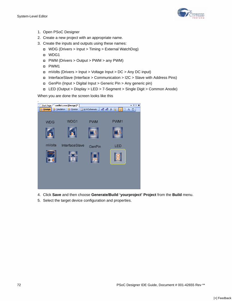
72 PSoC Designer IDE Guide, Document # 001-42655 Rev **
System-Level Editor
1. Open PSoC Designer2. Create a new project with an appropriate name.3. Create the inputs and outputs using these names:
WDG (Drivers > Input > Timing > External WatchDog)WDG1PWM (Drivers > Output > PWM > any PWM)PWM1mVolts (Drivers > Input > Voltage Input > DC > Any DC input)InterfaceSlave (Interface > Communication > I2C > Slave with Address Pins)GenPin (Input > Digital Input > Generic Pin > Any generic pin)LED (Output > Display > LED > 7-Segment > Single Digit > Common Anode)
When you are done the screen looks like this.
4. Click Save and then choose Generate/Build ‘yourproject’ Project from the Build menu.5. Select the target device configuration and properties.
[+] Feedback

PSoC Designer IDE Guide, Document # 001-42655 Rev ** 73
System-Level Editor
For this example select CY8C29466, 28-Pin PDIP/SSOP/SOIC.
Make certain to select Assign pins automatically.Click OK.
6. When the build system completes you see this screen.
Automatic pin assignment failed because of conflicts between the drivers. You now begin the process of manually assigning drivers to the unassigned pins so that you solve this problem.Now you place the unassigned drivers on of the available pins.
[+] Feedback

74 PSoC Designer IDE Guide, Document # 001-42655 Rev **
System-Level Editor
7. Clear all pin assignments by clicking the Unassign All Pins button.The result is a screen that looks like this.
All the drivers are now listed on the right of the screen as unassigned drivers.8. When you click a driver the ports to which you can assign it are highlighted in green. Begin with
LED_bit0.
9. Drag InterfaceSlave_i2c I2CsCLPin to pin 13. The SDAPin will automatically assign to pin 15.
[+] Feedback

PSoC Designer IDE Guide, Document # 001-42655 Rev ** 75
System-Level Editor
10.Select each of the other drivers and repeat the process until all the drivers are assigned and the screen looks like this.
The build is now complete and you are ready to move to the next step: programming the part.
The process illustrated here seems simple. You add inputs, outputs, and an interface. Then youselect a part and build the file. If there are conflicts such as encountered in this example you reas-sign the drivers and complete the process. PSoC Designer automatically takes care of all the under-lying complexity and puts everything in the proper place.
PSoC Designer creates a .soc file that allows you to open the project Interconnect view. This allowsyou to further customize your design. In addition you are able to use the interconnect view to see thecomplexity of your design. Here are two views of the pin assignment for this sample project.
[+] Feedback

76 PSoC Designer IDE Guide, Document # 001-42655 Rev **
System-Level Editor
Your seemingly simple design is, in fact, complex and ready for further customization.
3.12 Programming PSoC Flash MemoryWhen you are satisfied with your design and completed build, you need to program and test yourPSoC device.
Click Program to launch the PSoC Programmer application.Figure 3-10. PSoC Programmer Application
Table 3-3. PSoC Designer and PSoC Designer 4.3 Design Views
PSoC Express PSoC Designer 4.4
[+] Feedback

PSoC Designer IDE Guide, Document # 001-42655 Rev ** 77
System-Level Editor
The application loads with the PSoC Designer hex file in memory. Follow instructions in the PSoCProgrammer User Guide to program the PSoC device.
3.13 Monitoring Your DesignThe board monitor is a debugging tool similar to the simulation tab, except that it is designed to beused while attached to a prototype board through a communication interface that allows you to mon-itor changes in the various design elements in real time.
The default communication for the board monitor is I2C uses the CY3240-I2USB I2C to USB BridgeDebugging/Communication Kit. This allows you to monitor the board using the same ISSP (In Sys-tem Serial Programming) connector that you use to program it.
Figure 3-11. Monitoring Desktop
When you are done programming, exit the PSoC Programmer application. Not exiting the applica-tion may cause some communication errors between PSoC Designer and PSoC Programmer.
Monitor Controls
Widgets
[+] Feedback

78 PSoC Designer IDE Guide, Document # 001-42655 Rev **
System-Level Editor
The monitor desktop looks very similar to the simulation desktop, except that you are monitoring livevalues from your prototype board. The board monitor also enables the use of the variables chart win-dow that allows you to track any or all of your system variables in real time.
Figure 3-12. Variables Chart Window
The variables chart allows you to track all or any combination of system variables in real time on achart. You can choose which of the available variables appear in the chart window by checking orclearing the box next to the variable name.
The variables chart supports three different vertical scaling modes:
3.13.1 Monitoring Your Board With the I2C-USB Bridge
The easiest method of monitoring your board is to use the CY3240-I2USB I2C to USB BridgeDebugging/Communication Kit. The I2C to USB Bridge is a quick and easy link from any design orapplication’s I2C bus to a PC via USB for design testing, debugging and communication. 1. Open your design in PSoC Designer.
Table 3-4.
Automatic Scaling The Variables Window uses a preset algorithm to choose a scale that will allow all selected variables to be displayed.
Manual Scaling Deselect the Auto Scale box and enter a minimum and maximum value for the Y scale. Only those traces that fall within the selected range will be displayed.
Data Normalized to a Manual Scale
Select the Normalize button and all of the selected variables will be normalized so that they can be viewed on a common scale that you choose. Each variable is scaled according to that variables Minimum and Maximum. So if a variable has a max of 5 and a minimum of -5 and the actual values recorded range from -4 to 4, the data points will be graphed over the middle 80% of the chosen range.
[+] Feedback

PSoC Designer IDE Guide, Document # 001-42655 Rev ** 79
System-Level Editor
2. If your design does not already have an I2C interface, choose an I2C slave communication inter-face, and place it on your design. Leave the I2C_Address at the default value of 4.
3. When you do pin assignment for the project, the I2C pins will default to P1[7] and P1[5]. You will need to move them to P1[0] and P1[1].
4. Build your project and program your board.5. Switch to the Monitor desktop.
6. Plug the I2C-USB Bridge into your board. 7. Plug the USB cable into the I2C-USB Bridge.8. Plug the USB Cable into your PC.
The board monitor displays Connected.9. Choose the correct power setting.
Board Powered if the board has its own power5V Supplied or 3.3V Supplied to power the board from the USB bus.
10.Press the Play button to begin monitoring the board.The board monitor displays Running.
[+] Feedback

80 PSoC Designer IDE Guide, Document # 001-42655 Rev **
System-Level Editor
11. Interacting with the controls on the board will register in the board monitor in real time.
3.13.2 Monitoring Your Board with Other InterfacesIf you use USB, or some other interface in your design, you will need to write your own firmware tocommunicate with the board monitor.
3.14 Tuning Your DesignMost drivers in PSoC Designer are very simple. They have a few easily modifiable parameters, theresults of which are easy to predict. In many cases the simulation desktop is all that is needed tomake adjustments and get everything working as you expect. There are a few drivers, however, thathave complex settings, that interact with the real world in subtle ways, or both. These drivers requirein-circuit testing and modifications that were not previously possible with PSoC Designer. Examplesof this are capacitive sensing applications, and high brightness LEDs.
The parameters that you set in PSoC Designer are written to Flash memory on the PSoC device.The firmware loads these values into registers when the device boots. Normally, to change a param-eter setting on your prototype hardware, you make a change to the parameter in PSoC Designer,rebuild the project, and reprogram the part. This can be a time consuming process for complexdesigns that require multiple small changes to get them ‘just right.’
To help with this, PSoC Designer now has tuners available for a few of its more complex drivers. Atuner the result of a combination of some additional PSoC firmware and a custom visual interface. Ifa driver has a tuner associated with it, one of its properties will be Expose Tuning Values. SettingExpose Tuning Values to Yes adds a small loop to the firmware that periodically copies the param-eter settings from Flash to the associated register at run time. The visual interface of the tuner willallow you to both monitor the device at run time, and also make changes to properties and writethose parameter changes to Flash. You can then choose to write those values back to the parametersettings in PSoC Designer, or discard the changes and try again.
To enable tuning in your design, you must do two things in PSoC Designer:1. Set Expose Tuning Values to Yes for all drivers that you want to tune.
[+] Feedback

PSoC Designer IDE Guide, Document # 001-42655 Rev ** 81
System-Level Editor
2. Make sure that the Flash Interface is Enabled in the Device Configuration properties when you choose the device for your project.
Exposing tuning values adds some extra code to your design, so you may want to make sure thatyou set Expose Tuning Values to No before you do your final build, especially if resources are tightor you are trying to fit your final design into a smaller, less expensive part.
The following example shows the process of tuning a driver. This example shows tuning of aCapSense button on a CY3203 CSA CapSense board. To set it up, choose a CSA Properties driverto set global CSA properties, several CSA buttons, a Diplexed Slider, and an I2C interface. See thePSoC Express CapSense Guide for details on how to set up this project. Build the project and set upthe board monitor as shown in “Monitoring Your Design” on page 77.1. In the board monitor desktop, right click on a tunable driver.
[+] Feedback

82 PSoC Designer IDE Guide, Document # 001-42655 Rev **
System-Level Editor
The tuner window for the driver displays.
2. Touch the button on the board that corresponds to driver tuner displayed.The button is more sensitive than it needs to be.
3. Increase the Finger Threshold and increase the IDAC setting. The IDAC setting is inversely related to the sensitivity of the button. See driver datasheet for more information about the settings.
4. Click Apply to Board to write the changed parameter to Flash on the PSoC device.
[+] Feedback

PSoC Designer IDE Guide, Document # 001-42655 Rev ** 83
System-Level Editor
5. To see exactly where a button triggers you can move your finger slowly on to the button. Do this to observe that the Finger Threshold is higher now than it was before.
6. Place a finger fully on the button to observe that it is less sensitive now.
7. Click OK to save the values from the tuner window back to properties in PSoC Designer. Clicking Cancel discards your changes, and retains the original properties settings.
[+] Feedback

84 PSoC Designer IDE Guide, Document # 001-42655 Rev **
System-Level Editor
[+] Feedback

PSoC Designer IDE Guide, Document # 001-42655 Rev ** 85
4. Code Editor
In this chapter you learn how to create the project code.
4.1 File Definitions and Recommendations Once you complete your device configuration, you are ready to create the application code. This isdone in the Code Editor subsystem.
To access the Code Editor, double click any source file in the Workspace Explorer.
Figure 4-1. Code Editor View
The Workspace Explorer is shown in the right frame of Figure 4-1. This tree maintains the list of filesthat include configurations files, user module source and header files, boot files, and user applicationcode.
[+] Feedback

86 PSoC Designer IDE Guide, Document # 001-42655 Rev **
Code Editor
4.1.1 File Types and ExtensionsWhen you create a project, a root directory with three folders is generated at the location you spec-ify. The name of the root directory is the project name and the names of the three folders are lib(Library), obj (Objects), and output (for files generated by a project build).■ The lib folder contains user module Library Source files.■ The obj folder contains intermediate files generated during the compiling/assembling of .c and
assembly source files.■ The output folder contains the project.hex file (used for debugging and device programming), the
listing file, and other files that contain debug information.
Table 4-1 lists the PSoC Designer project file types and extensions. Most of these files are editableand appear in the left frame of the system interface inside the folder bearing the project name. Formore details regarding files and recommended usage see “Project File System” on page 87.
Table 4-1. File Types and Extensions
Type Extension Location Description
Address Map .mp …\output folder under project directory
Generated during the build process. Identifies global symbol addresses and other attributes of output.
ASM Includea .inc ASM Include Headers in source tree
Editable Assembly language include file (gen-erated for APIs).
Assembly of C .s Found near the C file Assembly generated from the C source code.
Assembly Sour-cea .asm Source Files\ Library
Source in source treeEditable assembly language source file (cre-ated initially, added, or generated for APIs).
C Header .h C Headers in source tree Editable language include file (generated for APIs).
C Sourcea .c Source Files in source tree Compiler language file that can be added to the project.
CFG File .cfg Folder under project direc-tory
Project configuration file that can be imported and exported for Dynamic Reconfiguration.
CMX File .cmx
Debug Symbols .dbg …\output folder under project directory
Generated during the build process. Used by the Debugger subsystem.
Full Program Listing .lst …\output folder under
project directoryFull program listing. Used by the Single-Step ASM function.
HEX File .hex …\output folder under project directory
Output file in Intel HEX format generated dur-ing the build process. This file alone will be downloaded to the ICE for project debugging.
Library/Archive .a …\lib\libpsoc.a but Librar-ies can be anyplace
A collection of object files, created by ilibw.exe.
Make .mk Menu under Project > Open local.mk file
Customize the Build/Make process for a partic-ular PSoC Designer project.
Object Module .o …\obj folder under project directory
Intermediate, relocatable object file generated during assembly and compilation.
Project Databasea .soc Project directory Project file accessed under File > Open
Project.
Relative Source Listing .lis …\obj folder under project
directoryRelative address listing file generated by the assembler.
[+] Feedback
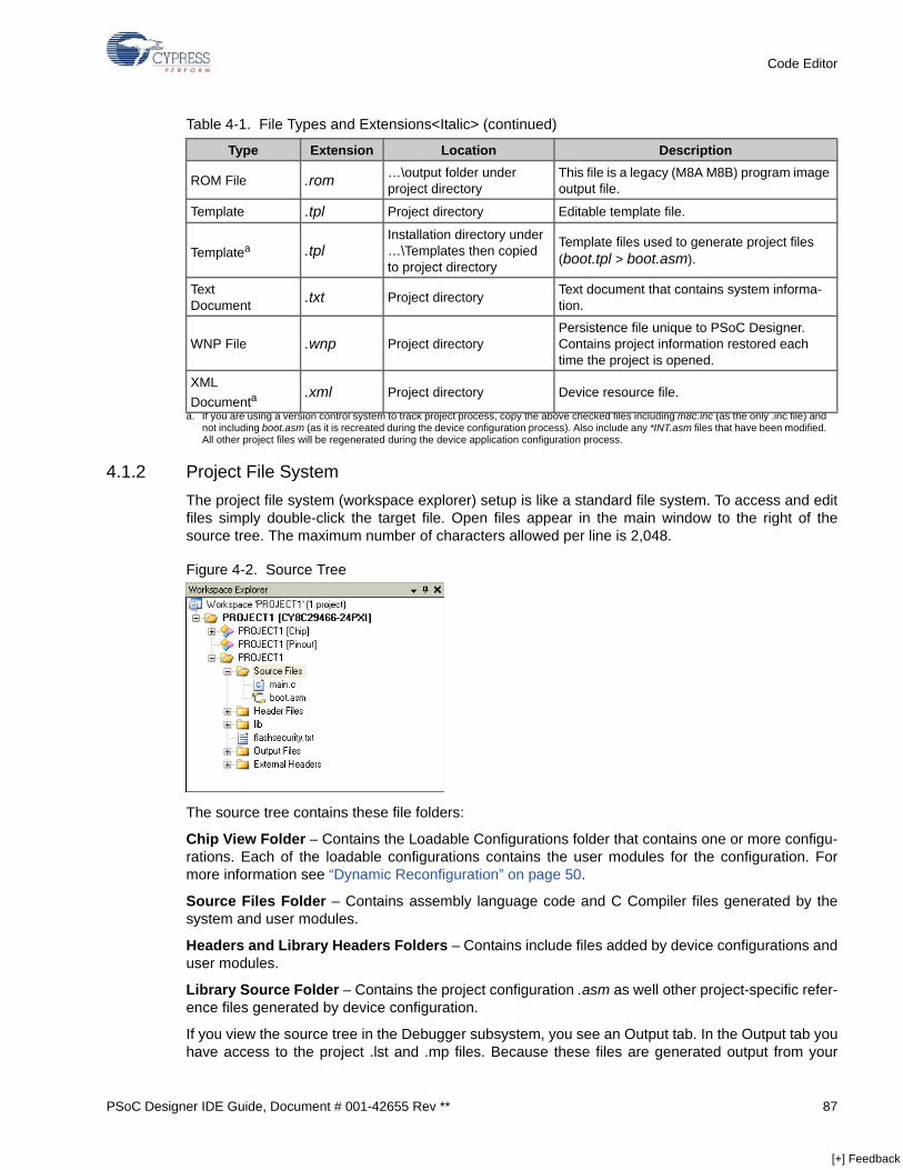
PSoC Designer IDE Guide, Document # 001-42655 Rev ** 87
Code Editor
4.1.2 Project File SystemThe project file system (workspace explorer) setup is like a standard file system. To access and editfiles simply double-click the target file. Open files appear in the main window to the right of thesource tree. The maximum number of characters allowed per line is 2,048.
Figure 4-2. Source Tree
The source tree contains these file folders:
Chip View Folder – Contains the Loadable Configurations folder that contains one or more configu-rations. Each of the loadable configurations contains the user modules for the configuration. Formore information see “Dynamic Reconfiguration” on page 50.
Source Files Folder – Contains assembly language code and C Compiler files generated by thesystem and user modules.
Headers and Library Headers Folders – Contains include files added by device configurations anduser modules.
Library Source Folder – Contains the project configuration .asm as well other project-specific refer-ence files generated by device configuration.
If you view the source tree in the Debugger subsystem, you see an Output tab. In the Output tab youhave access to the project .lst and .mp files. Because these files are generated output from your
ROM File .rom …\output folder under project directory
This file is a legacy (M8A M8B) program image output file.
Template .tpl Project directory Editable template file.
Templatea .tplInstallation directory under …\Templates then copied to project directory
Template files used to generate project files (boot.tpl > boot.asm).
Text Document .txt Project directory Text document that contains system informa-
tion.
WNP File .wnp Project directoryPersistence file unique to PSoC Designer. Contains project information restored each time the project is opened.
XML Documenta
.xml Project directory Device resource file.
a. If you are using a version control system to track project process, copy the above checked files including m8c.inc (as the only .inc file) andnot including boot.asm (as it is recreated during the device configuration process). Also include any *INT.asm files that have been modified.All other project files will be regenerated during the device application configuration process.
Table 4-1. File Types and Extensions<Italic> (continued)
Type Extension Location Description
[+] Feedback

88 PSoC Designer IDE Guide, Document # 001-42655 Rev **
Code Editor
assembled and linked source, they are read only. You can also access the Output tab on the sourcetree in the Code Editor by selecting Tools > Options > Code Editor tab and unchecking Enable Out-put.
4.1.3 boot.asmThis startup file resides in the source tree under Source Files and is important because it defines theboot sequence. The components of the boot sequence are: ■ Defines and allocates the reset and interrupt vectors.■ Initializes device configuration.■ Initializes C environment if using the C Compiler.■ Calls main to begin executing the application code.
When a project is created, the template file, boot.tpl, is copied into the project directory. Each timethe project is generated, the boot.asm file is generated from the local boot.tpl file.
boot.asm is re-generated every time device configurations change and application files are gener-ated. This is done to make certain that interrupt handlers are consistent with the configuration. If youmake changes to boot.asm that you do not want overwritten, modify the local project boot.tpl file andthen re-generate file.
4.1.4 main.asm/main.cIf the C complier is not enabled, then the main.asm file is generated for applications written inAssembly language. If the C Compiler is enabled, the main.c file is generated for a C program. Thisfile resides in the source tree under Source Files and is important because it holds the _main labelthat is referenced from the boot sequence.
4.1.5 PSoCConfig.asmThis is a required Library Source file because it contains the configuration that is loaded at systempower-up.
PSoC Designer overwrites PSocConfig.asm when a device configuration changes and applicationfiles are regenerated, with no exceptions. To manipulate bits, all part register values reside in this filefor your reference.
4.1.6 Additional Generated FilesAdditional files are generated in association with user modules and Dynamic Reconfiguration.
Psocgpioint.inc – This file contains additional information pertaining to pin GPIO write only registershadows. If a pin group is defined in a register set for which register shadows are allocated, then aset of three macros are defined for each register shadow to read, set, or clear the particular bit withinthe register associated with the pin. The names of the macros are keyed to the custom nameassigned to the pin and are:■ GetCustomName_registerName ■ SetCustomName_registerName ■ ClearCustomName_registerName
CustomName is the custom name set for the pin, and registerName is the associated registername for which a register shadow is allocated.
[+] Feedback

PSoC Designer IDE Guide, Document # 001-42655 Rev ** 89
Code Editor
The registerName registers vary with the chip device description and include all registers associatedwith the GPIO ports. For the CY8C25xxx/26xxx device family, registers include:■ Bypass■ DriveMode_0■ DriveMode_1■ IntCtrl_0■ intCtrl_1■ IntEn
For all other PSoC device families, registers include:■ GlobalSelect■ DriveMode_0■ DriveMode_1■ DriveMode_2■ IntCtrl_0■ IntCtrl_1■ IntEn
The register shadow allocation is determined by user modules and Dynamic Reconfiguration. As theregister allocation changes, the macro generation changes accordingly.
Psocgpioint.h – This file contains the same information as Psocgpioint.inc except that it is in a formneeded for C code. In the case of the register shadows, this file does not generate macros, butrather defines a symbol that allows manipulation of the shadow as a global variable. For each regis-ter shadow associated with a custom pin definition, a variable named CustomName_registerNameShadow is defined, where CustomName and registerName are the same aspreviously defined for Psocgpioint.inc. The variable name is then used to manipulate the shadowregister. For example, to set a pin value to ‘1’ within the port, do this:CustomName_registerNameShadow |= CustomName_MASK;CustomName_registerName_ADDR = CustomName_registerNameShadow;
Globalparams.h – This file has the same contents as globalparams.inc, except it also has #definestatements.
[+] Feedback

90 PSoC Designer IDE Guide, Document # 001-42655 Rev **
Code Editor
4.2 Working in Code EditorBefore you begin adding and modifying files, take a few moments to navigate Code Editor, takeinventory of your current files, and map out what you plan to do and how you plan to do it.
4.2.1 Modifying FilesWhen you are ready to program and modify assembly language source files, double-click the targetfile located in the file source tree. The file opens and appears in the main active window. You canopen multiple files simultaneously. Table 4-2 details the menu options available for modifying sourcefiles.
Table 4-2. Menu Options for Modifying Source FilesIcon Option Menu Shortcut Feature
Compile/Assemble Build > Compile [Ctrl] [F7]Compiles or assembles the open, active file (.c or .asm)
Build Current Project Build > Build ProjectGenerate and Build All Projects
Build > Generate/Build All Projects [Shift] [F6]
Build Build > Generate/Build cur-rent project [F6] Builds the entire project and
links applicable files
New File File > New [Ctrl] [N] Adds a new file to the project
Open File File > Open [Ctrl] [O] Opens an existing file in the project
Indent Indents specified text
Outdent Outdents specified text
Comment [Ctrl][E]+[C] Comments selected text
Uncomment [Ctrl][E]+[U] Uncomments selected text
Toggle Bookmark Edit > Bookmarks > Toggle Bookmark
[Ctrl] [B] + [T]
Toggles the bookmark: Sets/removes user-defined book-marks used to navigate source files
Clear Bookmarks Edit > Bookmarks > Clear Bookmarks
[Ctrl] [B] + [C]
Clears all user-defined book-marks
Next Bookmark Edit > Bookmarks > Next Bookmark
[Ctrl] [B] + [N] Goes to next bookmark
Previous Bookmark Edit > Bookmarks > Previous Bookmark
[Ctrl] [B] + [P] Goes to previous bookmark
Find Text Edit > Find and Replace [Ctrl] [F] Find specified text
Undo Edit > Undo [Ctrl] [Z] Undo last action
Redo Edit > Redo [Ctrl] [Y] Redo last action
[+] Feedback

PSoC Designer IDE Guide, Document # 001-42655 Rev ** 91
Code Editor
4.2.2 Adding New FilesTo add a file: 1. Click the New File icon or select File > New File.2. In the New File dialog box, select a file from the File types.3. In the Name field, type the name for the file.4. The current project directory is the default destination for your file. Uncheck the Add to current
project field and click Browse to identify a different location if you do not want the default. The Browse button is only enabled if you uncheck the Add to current project field.
Figure 4-3. New File Dialog Box
5. When finished, click OK.Your new file is added to the file source tree and appears in the main active window.
4.2.3 Adding Existing FilesYou are also able to add existing source files to your project (either C or assembly). Do this byaccessing Project > Add File and identifying the source file (by locating the file with the file dialog).Keep in mind that you add a copy of your original file to the project, not the original itself.
If the existing file you want to add is under a lib folder (…\lib), this file is added to the LibrarySource tree and resides in the lib folder of the project.
4.2.4 Removing FilesYou can remove files from your project in one of two ways:1. To remove the file, right-click on the file and select Delete.2. Access Project > Remove from Project or right-click the file in the source tree and select
Remove from Project ([Delete] key).
[+] Feedback

92 PSoC Designer IDE Guide, Document # 001-42655 Rev **
Code Editor
4.2.5 Searching FilesIn addition to the standard Find/Replace feature in PSoC Designer, you can search for specific textinside specific files. To search for text in any single file or combination of multiple files:1. Click Edit > Find and Replace.
Figure 4-4. Find and Replace Dialog Box
2. In the Find what field of the Find in Files dialog box, type or click the drop-arrow to choose a pre-viously searched word.Search by standard grep (Global Regular Expression Print) methods. Grep searches the input files for lines containing a match to a given pattern list. For options, see grep.pdf in the \Docu-mentation\Supporting Documents subdirectory of the PSoC Designer installation direc-tory.
3. In the In files/file types field, type or click the drop-arrow to choose a previously searched file or file type. Separate multiple files by using a comma.
4. Select the folder or files from the Look In menu or select the button button, to search a dif-ferent project directory than the directory of your current open project. When Look In is set to Current Document or All Open Documents, the File Types Filter is ignored.
5. Click a check in the specifics: Match whole word, Match case, Search subdirectories, and Search up, if desired.
6. When finished, click Find Next, Find In Files, or Mark All (to highlight all occurences of the found text). Click Close to close the Find in Files dialog box.
7. The results of the Find In Files search is diplayed in the Output window. Double-click to open the file. The cursor is placed at the beginning of the found text.
The Mark All and Replace All functions only work when Look In is set to Current Document or AllOpen Documents. It will not mark or replace text in unopened documents.
[+] Feedback

PSoC Designer IDE Guide, Document # 001-42655 Rev ** 93
5. Assembler
In this chapter you receive high-level guidance on programming assembly language source files forthe PSoC device. For comprehensive details, see the PSoC Designer Assembly Language UserGuide.
5.1 Accessing the AssemblerThe assembler is an application accessed from within PSoC Designer, much like the C Compiler.This application is run as a batch process. It operates on assembly language source to produce exe-cutable code. This code is then compiled and built into a single executable file that is downloadedinto the In-Circuit Emulator (ICE), where the functionality of the PSoC device is emulated anddebugged.
The project source files appear in the left frame, called the source tree. Double-click individual filesso they appear in the main active window where you add and modify code using the standard cut,copy, paste edit icons.
5.2 The M8C Microprocessor (MCU)The Microprocessor (MCU) is an enhanced 8-bit microprocessor core. It is optimized to be small andfast.
There are five internal registers, see Table 5-1. All registers are 8 bits wide except the PC, which iscomposed of two 8-bit registers (PCH and PCL) which together form a 16-bit register.
Table 5-1. MCU Internal RegistersRegister Abbreviation
Accumulator AFlag FIndex XStack Pointer SPProgram Counter PC
[+] Feedback

94 PSoC Designer IDE Guide, Document # 001-42655 Rev **
Assembler
5.2.1 Address SpacesThere are three separate address spaces implemented in the Assembler:■ Register Space (REG) – Accessed through the MOV and LOGICAL instructions. There are 8
address bits available to access the register space, plus an extended address bit via the Flag register bit 4.
■ Data RAM Space – Contains the data/program stack and space for variable storage. All the read and write instructions, as well as instructions which operate on the stacks, use data RAM space. Data RAM addresses are 8 bits wide.The M8C is able to directly access 256 bytes of RAM. Some PSoC devices have more than a 256-byte RAM page. These devices access multiple RAM pages using a combination of page mode bits in the Flag and Paging registers of the register address space. See the PSoC device data sheets and the PSoC Technical Reference Manual for details.
■ Program Memory Space – Organized into 256 byte pages, such that the PCH register contains the memory page number and the PCL register contains the offset into that memory page. The M8C automatically advances PCH when it needs to cross a page boundary. The user need not be concerned with program memory page boundaries, because they are invisible within the pro-gramming module. The one exception to this is that non-jump instructions ending on a page boundary take an extra cycle to complete. Jump instructions are not affected in this manner.
5.2.2 Instruction FormatInstruction addressing is divided into two groups:■ Logic, Arithmetic, and Data Movement Functions (Unconditional) –
These are 1-, 2-, or 3-byte instructions. The first byte of the instruction contains the opcode for that instruction. In 2-byte instructions, the second byte contains either a data value or an address.
■ Jump and Call Instructions, including INDEX (Conditional) –Most jumps, plus CALL and INDEX, are 2-byte instructions. The opcode is contained in the upper 4 bits of the first instruction byte and the destination address is stored in the remaining 12 bits. For program memory sizes larger than 4 KB, a 3-byte format is used.
5.2.3 Addressing ModesTen addressing modes are supported. For examples of each see the PSoC Designer Assembly Lan-guage User Guide.■ Source Immediate■ Source Direct■ Source Indexed■ Destination Direct■ Destination Indexed■ Destination Direct Immediate■ Destination Indexed Immediate■ Destination Direct Direct■ Source Indirect Post Increment■ Destination Indirect Post Increment
[+] Feedback

PSoC Designer IDE Guide, Document # 001-42655 Rev ** 95
Assembler
5.2.4 Destination of Instruction ResultsThe result of a given instruction is stored in the destination, which is placed next to the opcode in theassembly code. This allows for a given result to be stored in a location other than the accumulator.Direct and indexed addressed data RAM locations, as well as the X register, are additional destina-tions for some instructions. The AND instruction, in Table 5-2, is a good illustration of this feature(i2 = second instruction byte, i3 = third instruction byte). The ordering of the operands within theinstruction determines where the result of the instruction is stored.
5.3 Assembly File SyntaxAssembly language instructions reside in source files with .asm extensions in the source tree of theWorkspace Explorer. Each line of the source file may contain five keyword types of information.Table 5-3 supplies critical details about each keyword type.
Instructions in an assembly file have one operation on a single line. For readability, separate eachkeyword type by tabbing once or twice (approximately 5-10 white spaces). See the PSoC DesignerAssembly Language User Guide for type definitions and an example of assembly file syntax.
5.4 List File FormatWhen you build a project, a listing file with an .lst extension is created. The listing shows how theassembly program is mapped into a section of code beginning at address 0. The linking (building)process will resolve the final addresses. This file also provides a listing of errors and warnings, and areference table of labels.
.lst files are viewed after a project build in the Debugger subsystem under the Output tab of thesource tree.
Also generated during a build (in addition to the .lst file) are .rom, .mp, .dbg, and .hex files. The .hexis used for debugging and programming. The .mp contains global symbol addresses and otherattributes of output.
Table 5-2. Destination of AND InstructionSyntax Operation
AND A, expr acc ← acc & i2AND A, [expr] acc ← acc & [i2]AND A, [X + expr] acc ← acc & [x + i2]AND [expr], A [i2] ← acc & [i2]AND [X + expr], A [x + i2] ← acc & [x + i2]AND [expr], expr [i2] ← i3 & [i2]AND [X + expr], expr [x + i2] ← i3 & [x + i2]
Table 5-3. Keyword TypesKeyword Type Critical Details
Label A symbolic name followed by a colon (:)Mnemonic An assembly language keywordOperands Follows the MnemonicExpression Is usually addressing modes with labels and must be enclosed by parentheses
Comment Can follow Operands or Expressions and start in any column if the first non-space charac-ter is either a C++ style comment (//) or semicolon (;)
[+] Feedback

96 PSoC Designer IDE Guide, Document # 001-42655 Rev **
Assembler
5.5 Assembler DirectivesThe PSoC Designer Assembler allows the assembler directives listed in Table 5-4. See the PSoCDesigner Assembly Language User Guide for descriptions and sample listings of supported assem-bler directives.
Table 5-4. Assembler DirectivesSymbol Assembler Directive
AREA AreaASCIZ NULL Terminated ASCII StringBLK RAM Byte BlockBLKW RAM Word Block DB Define ByteDS Define ASCII StringDSU Define UNICODE StringDW Define Word DWL Define Word with Little Endian OrderingELSE Alternative Result of IF…ELSE…ENDIFENDIF End of IF…ELSE…ENDIFEQU Equate Label to Valuable ValueEXPORT ExportIF Conditional AssemblyINCLUDE Include Source File.LITERAL, .ENDLITERAL Prevent Code Compression of Data
MACRO/ENDM Macro Definition Start/EndORG Area Origin.SECTION, .ENDSECTION Section for Dead-Code Elimination
Suspend - OR F,0Resume - ADD SP,0 Suspend and Resume Code Compressor
[+] Feedback

PSoC Designer IDE Guide, Document # 001-42655 Rev ** 97
Assembler
5.6 Instruction Set To access a complete instruction in detail within PSoC Designer, click your cursor on the targetinstruction in the file and press [F1]. Table 5-5 lists the notation used for the instructions. See thePSoC Designer Assembly Language User Guide for the complete instruction set.
5.7 Compile and Assemble FilesOnce you complete programming all assembly language source (in addition to any .c source), youare ready to compile and assemble the group of files. Compiling translates source code into objectcode. (The Linker then combines modules and supplies real values to symbolic addresses, therebyproducing machine code.) Each time you compile and assemble, the most prominent, open sourcefile is compiled. PSoC Designer can decipher the difference between C and assembly languagefiles, and compile and assemble accordingly.
To compile the source files for your project, click the Compile/Assemble icon .
PSoC Designer employs a make utility. Each time you click the Compile/Assemble or Build icon, theutility automatically determines which files of a large application (manual or generated) were modi-fied and need recompiling, then issues commands to recompile them. For further details, seemake.pdf in the \Documentation\Supporting Documents subdirectory of the PSoC Designerinstallation directory.
Table 5-5. Instruction Set NotationNotation Description
A AccumulatorCF Carry Flagexpr ExpressionF Flags (ZF, CF, and Others)k Operand 1 Valuek1k2
First Operand of 2 OperandsSecond Operand of 2 Operands
PC PCH, PCLSP Stack PointerX X RegisterZF Zero Flag
[+] Feedback

98 PSoC Designer IDE Guide, Document # 001-42655 Rev **
Assembler
The Output Status (or error-tracking) window of Code Editor is where the status of file compiling andassembling resides. Each time you compile and assemble files, the Output Status window is clearedand the current status is entered as the process occurs.
Figure 5-1. Output Status Window
When compiling is complete, you the see the number of errors. Zero errors signify that the compila-tion and assemblage was successful. One or more errors indicate problems with one or more files.
This process reveals syntax errors. Such errors include missing input data and undeclaredidentifier. For a list of all identified compile (and build) errors with solutions see the PSoCDesigner Assembly Language User Guide. For further details on compiling and building see “Build-ing a Project” on page 101 in this guide.
At any time you can ensure a clean compile and assemble (or build) by accessing Project > Clean,then clicking the Compile/Assemble or Build icon. The “clean” deletes all lib\libPSoc.a,obj\*.o, and lib\obj\*.o files. These files are regenerated upon a compile or build (in additionto normal compile and build activity).
5.8 Calling Assembly Functions From CWhen one C function calls another, the compiler uses a simple layout for passing arguments that thecaller and callee use to initialize and the access the values. Although you can use the same layoutwhen a C function calls an assembly language routine, it is best to use of the alternate fastcall16calling convention. Fastcall16 is directly supported by the C compiler though use of a pragma direc-tive and is often more efficient than the convention used by C. In fact, fastcall16 is identical to the Ccalling convention except for simple cases when the parameters are passed and/or returned in theCPU A and X registers. All user module API functions implement the fastcall16 interface for this rea-son.
There are four conditions to meet when using the fastcall16 interface:■ The function must be tagged with a C #pragma fastcall16 directive■ The function needs a C function prototype■ The assembly function name must be the C function name prefixed with an underscore
character (_).■ The assembly function name must be exported.
[+] Feedback

PSoC Designer IDE Guide, Document # 001-42655 Rev ** 99
Assembler
For example, an assembly function that is passed a single byte as a parameter and has no returnvalue looks like this:
C function declaration (typically in a .h header file)#pragma fastcall16 send_bytevoid send_byte( char val);
C function call (in a .c file)send_byte( 0x37);
Assembly function definition (in an .asm file)export _send_byte; Fastcall16 inputs (single byte); A – data value; Fastcall16 return value (none)_send_byte:mov reg[ PRT1DR],Aret
An assembly function that is passed two bytes and returns one byte might look like this:
C function declaration (typically in a .h header file)#pragma fastcall16 read_indexed_regchar read_indexed_reg( char bank, char index);
C function call (in a .c file)val = read_indexed_reg( 0x01, index);
Assembly function definition (in an .asm file)export read_indexed_reg; Read byte from specified IO register; Fastcall16 inputs (two single bytes); A – bank number (0 or non-zero); X – register number; Fastcall16 return value (single byte); A – read data_read_indexed_reg: cpl A jnz get_data: or F, FLAG_XIO_MASK; switch to bank 1get_data: mov A, reg[X] and F, ~FLAG_XIO_MASK; make sure we’re in bank 0 ret
[+] Feedback

100 PSoC Designer IDE Guide, Document # 001-42655 Rev **
Assembler
Functions with more complex input parameters or return values can be written using these tables.
Note that the #pragma fastcall16 has replaced #pragma fastcall and use of #pragma fastcall is dep-recated.
Table 5-6. Pragma Fastcall16 Conventions for Argument Passing Argument Type Register Argument Register
Single Byte A The argument is passed in A.Two Single Bytes A, X The first argument is passed in A, the second in X.Double Byte X, A The MSB is passed in X, the LSB in A.Pointer A, X The MSB is passed in A, the LSB in X.
All Others None
Arguments are stored on the stack in standard byte order and in reverse order or appearance. In other words, the MSB of the last actual parameter is pushed first and the LSB of the first actual parameter is pushed last.
Table 5-7. Pragma Fastcall16 Conventions for Return Value
Return Type Return Register Comment
Single Byte A The argument is returned in A.Double Byte X, A The MSB is passed in X, the LSB in A.Pointer A, X The MSB is passed in A, the LSB in X.
All Others None Use a pass-by-reference parameter or global variable instead of returning arguments longer than 16 bits.
[+] Feedback

PSoC Designer IDE Guide, Document # 001-42655 Rev ** 101
6. Build Manager
In this chapter you learn the details of building a project, discover more about the C Compiler as wellas the basic, transparent functions of the system Linker and Loader, and Librarian. For comprehen-sive details on the C Compiler, see the PSoC Designer C Language Compiler User Guide.
6.1 Building a ProjectBuilding a project compiles and assembles all source files and selectively assembles library sourcefiles. The build process performs the compile and assemble of project files then links to all theproject’s object modules (and libraries), creating a .hex file that is easily downloaded for debugging.
Switching to the debugger causes the build process to recompile and link the project as needed.
To build the current project, either click the Build icon , select Build > Build from the menu, orpress [F7].
PSoC Designer uses GNU Make version 3.79 to manage the build process. Each time you click theCompile/Assemble or Build icon, make determines which source files were modified and issuescommands to recompile them and link the project.
For further details, see make.pdf in the \Documentation\Supporting Documents subdirectoryof PSoC Designer install directory.
The build process creates object modules in the obj or \lib\obj subdirectory of the project direc-tory.
The linking produces the final project image in the output folder of the project directory.
The .hex file can be downloaded to the ICE. Other files in the folder provide reference for you andthe Debugger subsystem. The .lst file contains a complete listing of the project, the .dbg file containsdebug information, the .mp file contains a memory map, and the .idata file contains initialized data.
At any time you can ensure a clean build by accessing Project > Clean then clicking the Build icon.The “clean” deletes all lib\libPSoc.a, obj\*.o and lib\obj\*.o files. These files are regen-erated on a build (in addition to normal build activity).
[+] Feedback

102 PSoC Designer IDE Guide, Document # 001-42655 Rev **
Build Manager
Each time you build your project, the Output Status window in Code Editor is cleared and the currentstatus is entered as the process occurs.
Figure 6-1. Output Status Window
When the build is complete, you see the number of errors and warnings. Zero errors signify a suc-cessful build. One or more errors indicate problems with one or more files. If there are errors, theprogram image (.hex file) is be available for download to the ICE. For a list of all identified compileand build errors with solutions see the PSoC Designer Assembly Language User Guide.
6.2 C CompilerIn addition to the development tools provided by Cypress Semiconductor, third party developmenttools are available for PSoC devices. This gives developers a choice of tools when working withPSoC devices. For information on how to install and use third party compilers with PSoC Designer,refer to documentation supplied by the manufacturer of the tool.
The iMAGEcraft compiler enables you to quickly create a complete C application for a PSoC device.Its built-in macro assembler allows assembly language code to seamlessly merge with C code.
The compiler compiles each .c source file to an .s assembly file. The assembler then translates each.asm or .s file into a relocatable object file, .o. After all the files are translated into object files, thebuilder and linker combine them together to form an executable file.
The iMAGEcraft C Compiler comes complete with embedded libraries providing port and bus opera-tions, standard keypad and display support, and extended math functionality. For comprehensivedetails on the C Compiler, see the PSoC Designer C Compiler User Guide.
6.3 LinkerThe linking functions in the build process are transparent to the user. Building your project links allthe programmed functionality of the source files (including device configuration) into a .hex file,which is the file used for downloading and debugging.
The linking process links intermediate object and library files generated during compilation andassembly, checks for unresolved labels, and then creates a .hex and a .lst file, as well as assorted .oand .dbg files. For descriptions of these files, refer to “Source Files Generated by Generate Applica-tion” on page 45.
[+] Feedback

PSoC Designer IDE Guide, Document # 001-42655 Rev ** 103
Build Manager
6.3.1 Customizing Linker ActionsTo customize the actions of the Linker, create a file called custom.lkp in the root folder of the project(see the Command Line Compiler Overview section in the PSoC Designer C Language CompilerUser Guide).
Be aware that in some cases, creating a text file and renaming it preserves the .txt file extension(e.g., custom.lkp.txt). If this occurs, you cannot use custom commands. The make reads the con-tents of custom.lkp and appends these commands to the Linker action.
A typical use for the custom.lkp capability is to define a custom relocatable code AREA. For exam-ple, to create code in a separate code AREA that should be located in the upper 2K of the Flash, usethis feature. For this example, the custom code AREA is called ‘BootLoader’. If you were developingcode in C for the BootLoader AREA, use this pragma in your C source file:
#pragma text:BootLoader// switch the code below from // AREA text to BootLoader// ... Add your Code ...#pragma text:text // switch back to the text// AREA
If you develop code in assembly, use the AREA directive in this manner:
AREA BootLoader(rom,rel); ... Add your Code ...AREA text ; reset the code AREA
Now that you have code that should be located in the BootLoader AREA, you can add your customLinker commands to custom.lkp. For this example, type this line in the custom.lkp file:
-bBootLoader:0x3800.0x3FFF
You can verify that your custom Linker settings were used by checking the Use verbose build mes-sages field in the Tools > Options > Builder tab. Build the project, then view the Linker settings in theBuild tab of the Output Status window (or check the location of the BootLoader AREA in the .mp file).
6.4 LibrarianThe library and archiving features of PSoC Designer provide system storage and reference.
There are two types of Librarian files (located in the source tree): Library Source and Library Head-ers. Source file types include archived and assembly language such as libPSoc.a and PSocCon-fig.asm. Header files are intermediate reference and include files created during application codegeneration and compilation. Both types are generated and used by PSoC Designer and are uniqueto each specific project.
[+] Feedback

104 PSoC Designer IDE Guide, Document # 001-42655 Rev **
Build Manager
[+] Feedback

PSoC Designer IDE Guide, Document # 001-42655 Rev ** 105
7. Debugger
In this chapter you learn how to download your project to the In-Circuit Emulator (ICE), use debugstrategies, and program the part. For additional information about the ICE and the development kit,refer to Application Note AN2018, Care and Feeding of ICE Pods at http://www.cypress.com/.
7.1 Debugger ComponentsThe PSoC Designer Debugger provides in-circuit emulation that allows you to test the project in ahardware environment, while viewing and debugging device activity in a software environment. ThePSoC In-Circuit Emulator (ICE) Debugging Kit contains these components as shown in Figure 7-1.Note that the CAT5 Patch Cable should be no longer than 1 foot. It must also have 8 wires in orderto connect from the ICE to the Pod (some data CAT5 cables have only four wires).
Figure 7-1. Basic Development Kit Components
There are separate user guides for two of the key debugger components:■ PSoC ICE User Guide■ PSoC Programmer User Guide
The PSoC ICE User Guide teaches you how to connect the ICE to your computer, configure the soft-ware to enable communication and debugging between PSoC Designer and the Pod, and trouble-shoot the ICE installation. The PSoC Programmer User Guide (referred in 7.6 “Programming thePart“ on page 119) teaches you how to open a HEX file, select a communication port, set a device,set a programming mode, program, verify, read, and run a checksum.
[+] Feedback

106 PSoC Designer IDE Guide, Document # 001-42655 Rev **
Debugger
7.2 Menu OptionsThe Debugger and ICE toolbars incorporate the most important Debugger functions.
A listing of all Debugger menu options is available in Table 7-1.
Table 7-1. Debugging Menu OptionsIcon Menu/Tool Tip Shortcut Feature
Connect Connects PSoC Designer to ICE
Download to Emulator
Downloads project .hex file to hardware emulator (Pod). This file holds all device configurations and source-code functionality
Execute Program
Switches into Debugging subsystem, connects, down-loads .hex, runs... all from one click
Go [F5] Starts debugger
Run to Cursor [F6]Creates a temporary (invisible) breakpoint at the current cursor location in the source code and runs the applica-tion to that point.
Stop/Halt [Shift][F5] Stops debugger
Reset [Ctrl] [Shift] [F5] Resets the device to a PC value of ‘0’ and restarts the debugger
Step Intoa
a. If C source lines are compiled into assembly code that branches the execution path (such as lcall or call instructions), the Debuggerattempts to step into the source file of the destination address. For library code such as multiplication and division, a call to the libraryassembly code is made but the original source file is not available in the project. Step Into then gives the message “No source availablefor step operation.” Step Over can be used instead of step into for this situation.
[F11] Steps into next statement
Step Out [Shift] [F11] Steps out of current function
Step Overa [F10] Steps over next statement
Step ASM [Shift][F10] If the current line of code is C code, the line is located in the .lst file and that line is executed.
Refresh M8C Views
Refreshes the data in the Memory, CPU Registers, and Watch Variables debugger windows with current data from the emulator.
Get Next Trace Data
When the debugger halts, the trace data window is loaded with the latest 64 lines of trace data. This button retrieves an additional 64 lines.
[+] Feedback

PSoC Designer IDE Guide, Document # 001-42655 Rev ** 107
Debugger
7.3 Connecting to the ICEYou must establish a communication link between the PC and the ICE. This is done by choosing theappropriate ‘port’. To make the Debugger port selection select the Project > Settings > Debuggertab.
Figure 7-2. Debugger Project Settings - LPT1
The “ICE connected to:” list shows parallel ports (i.e., LPT1…3) supporting the original PSoC ICE.The definition of the USB ports are determined by this coding:
USB/yywwTxxx
Where:yy: Year the ICE was manufacturedww: Work week the ICE was manufacturedT: Type of USB connection where:
C: ICE CubeD: USB Adapter/Dongle for a legacy ICE
xxx: Manufacturing sequence number
Once you have set your debugger port, and are connected to your ICE, check the PC to ICE com-
munication link by using the Connect button or by selecting the Debug > Connect/Disconnectmenu item. The results of the connection attempt are displayed in the Output window. A successfulconnection displays this message:
The status bar shown in Figure 7-3 also shows information associated with debugging.
Figure 7-3. Debug Status Bar.
Connecting . . .
ICE Port: USB/0611C003
Pod powered by the ICE
Connected.
[+] Feedback

108 PSoC Designer IDE Guide, Document # 001-42655 Rev **
Debugger
7.4 Downloading to the PodBefore you begin a debug session you need to download your project .hex file to the pod. By doingthis, you load the ROM addressing data into the emulation bondout device (chip on the pod). A gen-eral rule to follow before downloading is to make sure there is not a part in the programming socketof the Pod. Otherwise, debug sessions may fail.
To download the .hex file to the Pod:
1. Click the Download to Emulator (Pod) icon . The system downloads the project .hex file located in the …\output folder of your project direc-tory. A progress indicator reports download status.
2. Once the download is complete, the pod can be directly connected to and debugged on your spe-cific circuit board.
If you cannot debug your project with the current pod, you receive this message:This project is incompatible with the Pod/Chip.
This appears in the Debug tab of the Output Status window:Unable to connect to ICE due to pod incompatibility with project.Found: debugger version 6a, pod ID 8, pod micro CY8C25/26xxx rev DCheck the Project/Pod compatibility document.
[+] Feedback

PSoC Designer IDE Guide, Document # 001-42655 Rev ** 109
Debugger
7.5 Debug StrategiesDebugger commands allow you to read and write program and data memory, read and write IO reg-isters, read and write CPU registers and RAM, set and clear breakpoints, and provide program run,halt, and step control.
Figure 7-4. Debugger Subsystem View
In the status bar of the Debugger subsystem you find ICE connection indication, debugger targetstate information, and Accumulator, X, Stack Pointer, Program Counter, and Flag register values.
Source TreeWindow
Main Menu/ToolbarsArea
OutputWindow
EditWindow
MemoryWindow
Watch VariableWindow
Break PointsWindow
RegistersWindow
[+] Feedback

110 PSoC Designer IDE Guide, Document # 001-42655 Rev **
Debugger
To help with troubleshooting, you can view your application source files inside the Debugger sub-system. If the project source tree is not showing, click View > Workspace Explorer.
The project files that you view in the debugger will be read-only while the debugger is running orhalted at a breakpoint. The source files are editable when the debugger is reset.
7.5.1 TraceThe Trace feature enables you to track and log device activity at either a high or detailed level. Suchactivity includes register values, data memory, and time stamps.
The Trace window is displayed when Debug > Windows > Trace is chosen.
The Trace window displays a continuous, configurable listing of project symbols and operations fromthe last breakpoint. (The trace shows symbolic, rather than address data, to enhance readability.)Each time program execution starts, the trace buffer is cleared. When the trace buffer becomes full,it continues to operate and overwrite old data.
Figure 7-5. Trace Window
Configure the Trace window by selecting either Debug > Trace Mode or Tools > Options from themenu. Configuration options include:
PC Only – Lists the PC value and instruction only.
PC/Registers – Lists the PC, instruction, data, A register, X register, SP register, F register, and ICEexternal input.
PC/Timestamp – Lists the PC, instruction, A register, ICE external input, and time stamp.
You can save the trace as a text file by selecting File > Save Trace.txt or File > Save Trace.txt as.
[+] Feedback

PSoC Designer IDE Guide, Document # 001-42655 Rev ** 111
Debugger
The trace log entries are logged before the instruction is executed. The contents of those entries are:■ PC Register■ A Register■ Data Bus■ External Signals
When using the ICE-4000, the external input value is the binary representation of the 8 center pinson the 10-pin ICE header. The right and left outside pins are connected to ground while the inputsaccept a 5-volt TTL level signal. The time stamp is displayed as a 32-bit relative count of clock cyclesfrom the CPU clock source.
The default size of trace is 256 kilobytes. This provides 128K trace instructions in trace mode 1 and32K trace instructions in trace modes 2 and 3.
7.5.2 Break PointsThe Break Point feature allows you to stop program execution at predetermined address locations.When a break point is encountered, the program stops at the address of the break point, withoutexecuting the address code. Once halted, the program is restarted using the available menu or iconoptions.
To set break points, first open the file to debug. Do this from the Workspace Explorer. (If your projectfile Workspace Explorer is currently not showing, click View > Workspace Explorer.) Break points arecreated by right clicking your mouse at targeted points and selecting Insert Break Point. You canview and remove active break points in the Break Points window. To open the Break Points window,select Debug > Windows > Break Points.
Figure 7-6. Debug Break Points Window
You can also view the exact line and column for each break point (or wherever you click your cursorin the file) across the bottom of PSoC Designer.
[+] Feedback

112 PSoC Designer IDE Guide, Document # 001-42655 Rev **
Debugger
7.5.3 CPU and Register Views There are five areas that are readable and writeable during debugging: CPU Registers, Bank Regis-ters 0, Bank Registers 1, RAM, and Flash. The CPU Registers are shown in their own window(Debug > Windows > Registers) and in the notification area at the bottom of PSoC Designer. Theother four areas can be viewed in the Memory Window (Debug > Windows > Memory). Select one ofthe four memory areas from the Address Space box. Each is described below.
NOTE: Use caution when changing register values; they can alter hardware functions.
CPU Registers – This window allows you to examine and change the contents of the CPU registers.Click the drop-arrow to access a register, then double-click and type over the value. Data is enteredin hexadecimal notation. CPU register values can be viewed across the bottom of PSoC Designer.
Bank Registers 0 and 1 – You can scroll through the register bank to view the values in the registerbank. Type a new value into the Offset to scroll directly to that offset. Click next to a value and typea new value for the register. All values must be entered in hexadecimal notation.
Note that you cannot change some registers because they are read only. Some registers are writeonly and cannot be read.
Figure 7-7. Bank 0 Registers in the Memory Window
RAM – View a RAM memory page. RAM locations can be modified by clicking the data at the spe-cific location and typing in the new value. Data is entered in hexadecimal notation.
Flash – The Flash window displays the data stored in Flash. This is the program memory; it is readonly.
The current status of all locations can be saved to a .txt file by right-clicking at the top of the windowand selecting Save or Save As.
[+] Feedback

PSoC Designer IDE Guide, Document # 001-42655 Rev ** 113
Debugger
7.5.4 Watch VariablesWatch Variables can be set by right clicking a variable in a source file and selecting Add Watch. Youcan also select Global Variables.
Right-click Add, Delete, or Properties in the Watch/Global Name window to add, delete, or modifyvalues. Note that if you change a variable type (or other settings in the window) and close theproject, the next time you access that project the variable types and settings are the same.
Figure 7-8. Watch Variables Window
By default, all variable values are shown in hexadecimal. Right-click inside the Watch Variables win-dow to display the toggle to show variable values in decimal instead. When the value of a watch vari-able changes (during program execution), the changed values are presented in red. Values that didnot change during the execution are presented in black.
If the selected watch variable is not within the current context of the debugger, the variable is shownas disabled. Once you have a program with Local Variables and the Debugger has halted in a func-tion where they are contained, you see the value of the variable.
You cannot change Variable names. You can cut, copy, paste, and delete values (not names) whenthe debugger is halted in a context where the variable exists. Double-click to highlight then righting-click to choose an option. The variable will be shown in red if it is stored in Flash. You cannot alterthe value of variables stored in Flash in the Watch Variable window. For better viewing, you canadjust the column width of the Local Name window by dragging the heading row column dividers.
The default action for using the Delete option is to set the value to zero (including Floating pointtypes).
The Local Variables are not “alive” when the program has halted at the initial function scope, forexample: void cgentest_009(void) {-------------------------- HALT, NO Locals uInt32 u32var0; uInt32 u32var1
-.-.-.-.-.-.-.-.-.-. etc -.-.-.-.-.-.-.-.-.-.
As discussed in “Menu Options” on page 106, you can use the Single Step icon to step through theproject .lst file.
7.5.4.1 Array Types Added to Global and Local Watch Variables
Array types were added to both Global and Local Watch Variables. Global and Local Watch Variablearray types must originate in C and not be exported from an .asm file. For example://--------------------------------
[+] Feedback

114 PSoC Designer IDE Guide, Document # 001-42655 Rev **
Debugger
char sC[5];signed char signedC[5];int siI[5];unsigned int uiI[5]; float fA[5];long slL[5]; unsigned long uslL[5];//-------------------------------
The example above shows declarations for all the supported array types.
The elements are displayed horizontally, separated by commas in both the Watch/Global Name andLocal Name windows. The radix can be changed from decimal to hexadecimal for all array typesexcept floats.
7.5.5 Dynamic Event PointsThe Events window is selectable by clicking Debug > Events. It allows you to perform complexdebugging by configuring conditional breaks and traces.
While breakpoints allow you to select a program location and halt, Dynamic Event Points providemultiple sequences of logical combinations and have multiple potential actions. Breakpoints allowyou to select locations within a program to stop, look around, and determine, “How did I get here?”However, debugging is enhanced by the ability to stop and collect information about the target pro-gram based upon specified conditions. An example scenario is “when variable OutputV gets set tozero, turn trace buffer on.”
Dynamic Event Points help simplify the debugging process by providing this capability. They monitorthe processor to determine a match with logical operations of Program Counter (PC), data bus, dataaddress, instruction type, external logic signals, X Register, Accumulator, Stack Pointer, and Flags.
Typically, breakpoints have one logical input (PC) and one action (Break). Dynamic Event Points, onthe other hand, trigger actions when the specified logical condition occurs. An event point can triggerthe following actions: break, turn trace on or off, decrement the input counter, initiate an external trig-ger, trigger the trace buffer, and enable an event sequence (these actions are triggered only with theICE-4000).
In summary, Dynamic Event Points provide you with the ability to:■ Define complex breakpoints.■ Characterize multiple test cases to be monitored and logically sequenced.■ Perform any of the following actions: break, turn the trace on, turn the trace off, or set an external
trigger using the ICE-4000.
7.5.5.1 Configuring Events
Use the Events Window to enable or disable event settings anytime during a debug session. To con-figure events:1. Click Debug > Windows > Events to access debugger events.2. Click your cursor in the first row, labeled ‘0’.3. Below the rows are options for 8 and 16 bit threads. Check one or both depending on the needs
of your project. Enabling both thread options activates the Combinatorial Operator field.4. Fill in the applicable thread fields (i.e., Low Compare, Input Select, High Compare, Input Mask),
as well as state logic fields (i.e., Next State, Match Count).
[+] Feedback

PSoC Designer IDE Guide, Document # 001-42655 Rev ** 115
Debugger
As you make your selection in the Input Select drop-down, you see details in the grayed-out, scrollable box below. Also, use Match Count to specify the number of times an event task occurs before it performs the selected action.The input mask for 8-bit threads is applied to the high and low range comparison values, as well as to the input select value. This is done to support range comparisons on subsets of the bits in the input select value. All comparisons take place within the bits specified by the input mask. Other bits are ignored.The range values are masked during event editing when the thread states are saved by the Apply button or by switching to a thread state. For example, if the entered low compare value is 06 HEX and the input mask value is 05 HEX, the low compare value after the mask is applied is 04 HEX. The input select value is masked at run time.
5. When finished, click Apply. The individual event is now configured and its information appears at row 0.If you forget to apply your entries, you are prompted to save. Click Yes or No.To clear all events in the dialog box, click Clear All. To disable all events in the dialog box, click Disable All.
6. Click row 1 and repeat steps 3-5 to configure another event. Repeat this process for each addi-tional event. (You can configure up to 65 events.)
7. Click Close to exit the dialog box. All entries are saved.
As you run events, you can view messages regarding the status in the Debug tab of the Output Sta-tus window. For instance, if you check Break as part of an event, “Hit Event state break” appears inthe Output Status window as the debugger hits the event.
For complete training on debugging and Dynamic Event Points, try PSoC Designer Module 3:Debugging with PSoC. Review and sign up under Training > On-Demand at http://www.cypress.com/.
7.5.5.2 Typical Event Uses
The many potential uses for events include:■ Find a stack overflow. See Stack Overflow Errors under Invalid Memory Reference in PSoC
Designer Online Help System at Help > Help Topics.■ Detect jmp or call out of program. See Code that will Corrupt Stack under Invalid Memory Ref-
erence in PSoC Designer Online Help System at Help > Help Topics.■ Trace a specific range of code.■ Find when a register is written (with optional matching data value).■ Drive an external signal on interrupt(s) using the ICE-4000.■ Measure interrupt latency.■ Break the ‘n’th time a line of code is executed (match count).■ Break on Carry Flag status.■ Break on signals from customer target board.■ Wait for certain number of instructions.■ Count sleep periods.■ Break on specific data in Accumulator on certain instructions (PC).■ Collect trace data reads or writes to specified register.■ Find memory write.
[+] Feedback

116 PSoC Designer IDE Guide, Document # 001-42655 Rev **
Debugger
7.5.5.3 Event Examples
Here are a few examples for common events.
Find Memory WriteTo break on a memory write to address 20h, execute the following example steps.1. Access the Debugger Events dialog box by clicking Debug > Windows > Events.2. Choose BITFIELD in the Parameter box.
The small help box in the lower left describes the BITFIELD input. Bit 1 is the RAM write flag.3. Bit 1 is the focus bit of this example; therefore, you need to mask the other bits. The Input Mask
field allows you to hide bits that you do not care about. It is an 8-bit number. Set bits in the input mask to mark the bits that you care about (e.g., 0F to get the low four bits, FF to get all eight bits, 01 to get the low bit, 80 to get the high bit, C0 to get the top two bits, etc.). Pick 02 for the input mask to get the RAM write bit.
4. Any masked bits need to be zeros in the compare fields. You can see in the help box that the focus bit is active low. It is a ‘0’ when the RAM write is happening. This means you can just set both compare values to ‘0’.
5. Pick MEM_DA for the input select. (If you picked MEM_DA_DB, you could check the address and the data value.) Note that this selection is different for the ICE Cube support of the CY8C29x66 devices.
6. Set both compare values to ‘20’, your desired address.7. Pick AND for your Combinatorial Operator.8. Press the Break check box. This makes the debugger halt when it sees the RAM write.9. Click Apply.
Stack OverflowTo create an event to break when the Stack Pointer reaches FF:
[+] Feedback
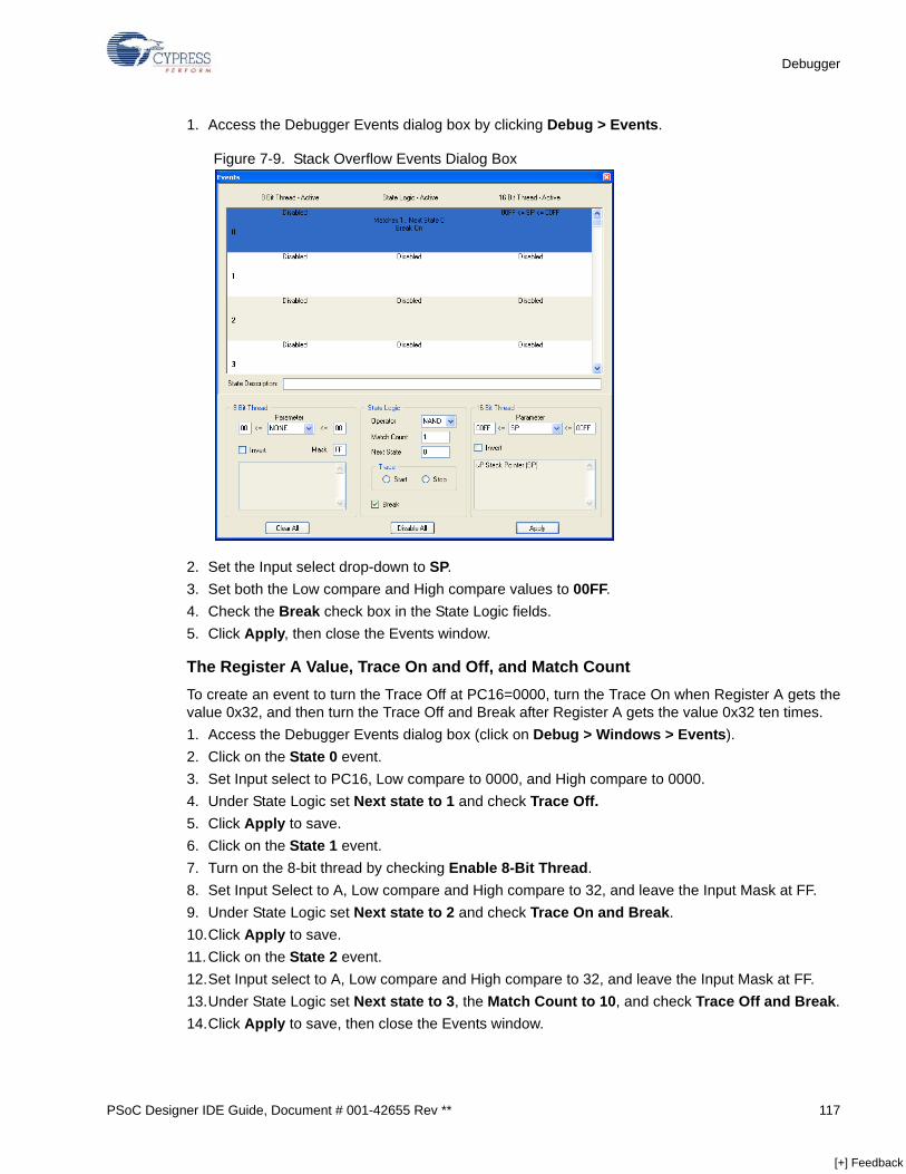
PSoC Designer IDE Guide, Document # 001-42655 Rev ** 117
Debugger
1. Access the Debugger Events dialog box by clicking Debug > Events.
Figure 7-9. Stack Overflow Events Dialog Box
2. Set the Input select drop-down to SP.3. Set both the Low compare and High compare values to 00FF.4. Check the Break check box in the State Logic fields.5. Click Apply, then close the Events window.
The Register A Value, Trace On and Off, and Match CountTo create an event to turn the Trace Off at PC16=0000, turn the Trace On when Register A gets thevalue 0x32, and then turn the Trace Off and Break after Register A gets the value 0x32 ten times.1. Access the Debugger Events dialog box (click on Debug > Windows > Events).2. Click on the State 0 event.3. Set Input select to PC16, Low compare to 0000, and High compare to 0000.4. Under State Logic set Next state to 1 and check Trace Off.5. Click Apply to save.6. Click on the State 1 event.7. Turn on the 8-bit thread by checking Enable 8-Bit Thread.8. Set Input Select to A, Low compare and High compare to 32, and leave the Input Mask at FF.9. Under State Logic set Next state to 2 and check Trace On and Break.10.Click Apply to save.11.Click on the State 2 event.12.Set Input select to A, Low compare and High compare to 32, and leave the Input Mask at FF.13.Under State Logic set Next state to 3, the Match Count to 10, and check Trace Off and Break.14.Click Apply to save, then close the Events window.
[+] Feedback

118 PSoC Designer IDE Guide, Document # 001-42655 Rev **
Debugger
7.5.6 End Point DataIf your project includes one of the USB user modules, you can display USB endpoint data capturedfrom the emulator in a debug window. To do so, select Debug > Windows > USB Endpoint Data. Thiscreates a file named USB Data.txt that captures and displays endpoint data every time the debuggeris halted.
To define Areas, use Debug > Configure USB Data Tracking.
For example:PMA0_WA: 00 PMA0_RA: 00 PMA1_WA: 00 PMA1_RA: 00 PMA2_WA: 00 PMA2_RA: 00 PMA3_WA: 00 PMA3_RA: 00 PMA4_WA: 00 PMA4_RA: 00 PMA5_WA: 00 PMA5_RA: 00 PMA6_WA: 00 PMA6_RA: 00 PMA7_WA: 00 PMA7_RA: 00
Area 1 Data...0x00: 8A 47 6F 84 35 2A 01 28 14 46 00 93 F3 B3 5D 600x10: B8 6C C4 A8 31 71 19 41 99 4A 89 AC CE 11 8D 280x20: 06 9D 43 8D 22 EE 6C 92 88 3B 33 61 93 A0 16 270x30: 8C 0C 9A F0 AA 21 E4 62 80 FA 48 C6 9E E3 66 220x40: C8 31 02 8E 14 50 5A 74 AB 38 6F 15 6C 21 E4 DA0x50: E5 A0 00 1A 0E EA C1 6E 59 46 9A 50 33 06 1F 980x60: 8E C3 F4 30 FD 12 01 43 38 52 95 20 D1 EF 71 940x70: 1C F8 7B 52 97 E6 12 3C 0C 56 92 2C 89 05 B5 D60x80: 1A 1A 80 0B 1E 09 48 3D 4E AB 38 2C CA 42 B4 3A0x90: 33 DB 13 A3 44 D9 8B 3B 51 DC 00 2D 1D A3 BD 320xA0: 01 E7 A1 24 4A 99 04 D8 83 63 C4 EF 88 4A 28 180xB0: 48 81 96 16 51 1C F3 9D 1C 2F 92 36 2A AE 5F 6D0xC0: 9C BC 0A FC D5 17 96 CF 61 20 FD 14 C4 09 E4 570xD0: D2 6C 51 36 3E AE 19 E2 99 5E 04 A1 C6 A9 D1 D00xE0: 5E 2D C1 70 97 F5 73 61 57 00 3D CB 77 E5 97 330xF0: 33 34 84 C7 2E 82 07 EA 76 9C 24 63 2B 7D 41 20
Area 2 Data...0x03: 84 35 2A 01
Area 3 has zero length
Area 4 has zero length
[+] Feedback

PSoC Designer IDE Guide, Document # 001-42655 Rev ** 119
Debugger
7.6 Programming the PartProgramming the part is done once debugging is complete. By doing this, you store the ROM datadirectly in the Flash memory of the part. The Cypress device can be reprogrammed many times dueto its Flash Program Memory. Figure 7-10 shows the Pod Programming Socket that is connected toa CAT5 cable.
Only the five required serial programming pins are available on the programming socket. Theserequired pins are the same pins that make up the Serial Programming Header (Vdd, Vss, XRES,P1[1] SCLK, and P1[0] SDATA). You cannot use the programming socket for emulation. Note theposition of Pin 1 on the programming socket to ensure correct operation.
Figure 7-10. ICE Cube and YProgrammer
Make sure the pod is not connected to a circuit board (your development board or the PSoC pup)when you program the part. Otherwise, programming (the part) may fail.
To program the part, place the part in the programming socket on the pod, then select Program >PSoC Programmer to launch PSoC Programmer. PSoC Programmer is a standalone device pro-gramming application. If PSoC Programmer is not installed, the icon is grayed out. It can be down-loaded from the Cypress web site. Using this PSoC Designer accessory you can quickly program,read, verify, and checksum. Refer to the PSoC Programmer’s User Guide for additional information.
[+] Feedback

120 PSoC Designer IDE Guide, Document # 001-42655 Rev **
Debugger
Alternatively, the device can be programmed on the target board using the Serial ProgrammingHeader on the Pod. The five connections that must be made from the Serial Programming Header tothe pins on the target device are listed in Table 7-2.
NOTE: Note: It is important to note that there is a limit to the amount of current that can be suppliedto the Vdd pin from the emulator pod (500 mA at 5V). If you draw greater current through the Vdd pinon the programming header, this could damage the emulator. You must supply the connections onthe target board for serial programming in the system.
Once part programming is complete, you test the program part directly on your development circuitboard.
Table 7-2. Header to Device Pin ConnectionsHeader Pin Device Pin
1 Vdd2 Vss3 XRES4 P1 [1]/SCLK5 P1 [0]/SDATA
[+] Feedback

PSoC Designer IDE Guide, Document # 001-42655 Rev ** 121
8. Flash Protection
Flash Program Memory Protection (FPMP) allows you to select one of four protection (or security)modes for each 64-byte block within the Flash, based upon the particular application.
8.1 FPMP and PSoC DesignerPSoC Designer has a rudimentary mechanism that enables you to set security modes in your Flashprogram memory. The security (or protection) is set from within PSoC Designer on a per projectbasis. The protection mechanism is implemented using the System Supervisor Call instruction(SSC). When this command is executed, two bits of data programmed into the Flash selects the pro-tection mode. Table 8-1 lists the available protection options.
A simple text file called flashsecurity.txt is used as the medium for the Flash security. This text filecontains comments describing how to alter the Flash security. PSoC Designer validates the correct-ness of the Flash security data before it is used.
NOTE: The flashsecurity.txt file for PSoC Designer v. 2.xx and higher projects that use Flash writesmust be set to the correct protection modes. The defaults are set to full-protect mode. To change theprotection mode, the part must be bulk erased and re-programmed using the flash security settings.
Table 8-1. Flash Program Memory Protection OptionsMode Bits Mode Name External Read External Write Internal Write Mode Code
00 Unprotected Enabled Enabled Enabled U01 Factory Upgrade Disabled Enabled Enabled F10 Field Upgrade Disabled Disabled Enabled R11 Full Protection Disabled Disabled Disabled W
[+] Feedback

122 PSoC Designer IDE Guide, Document # 001-42655 Rev **
Flash Protection
8.2 About flashsecurity.txtThe FPMP file, flashsecurity.txt, is added to each new project and appears in the WorkspaceExplorer.
Figure 8-1. flashsecurity.txt in Source Tree
PSoC Designer also adds the FPMP file to a cloned project. This is especially useful when cloningprojects created with earlier versions of PSoC Designer because earlier versions did not carry thisfeature. Note that if you do clone a project created in an earlier version of PSoC Designer, you areprompted to update your project, (see “Updating Existing Projects” on page 19).
NOTE: If, for some reason, flashsecurity.txt is missing or was deleted from the project, the defaultbehavior is to apply Mode Bit 11 Full Protection to the entire program memory.
This information contains instructions on modifying flashsecurity.txt and appears at the beginning ofthis file in PSoC Designer.; Edit this file to adjust the Flash security for this project.; Flash security is provided by marking a 64-byte block with a ; character that corresponds to the type of security for that ; block, given:;; W: Full (Write protected); R: Field Upgrade (Read protected); U: Unprotected; F: Factory
; Note #1: Protection characters can be entered in upper or ; lower case.; Note #2: Refer to the Flash Program Memory Protection section ; in the Data Sheet.
; Various parts with different Flash sizes can be used with ; this file. Security settings for Flash areas beyond the part ; limit will be ignored.; Comments may be added similar to an assembly language ; comment, by using the semicolon (;) followed by your comment.; The comment extends to the end of the line.
[+] Feedback
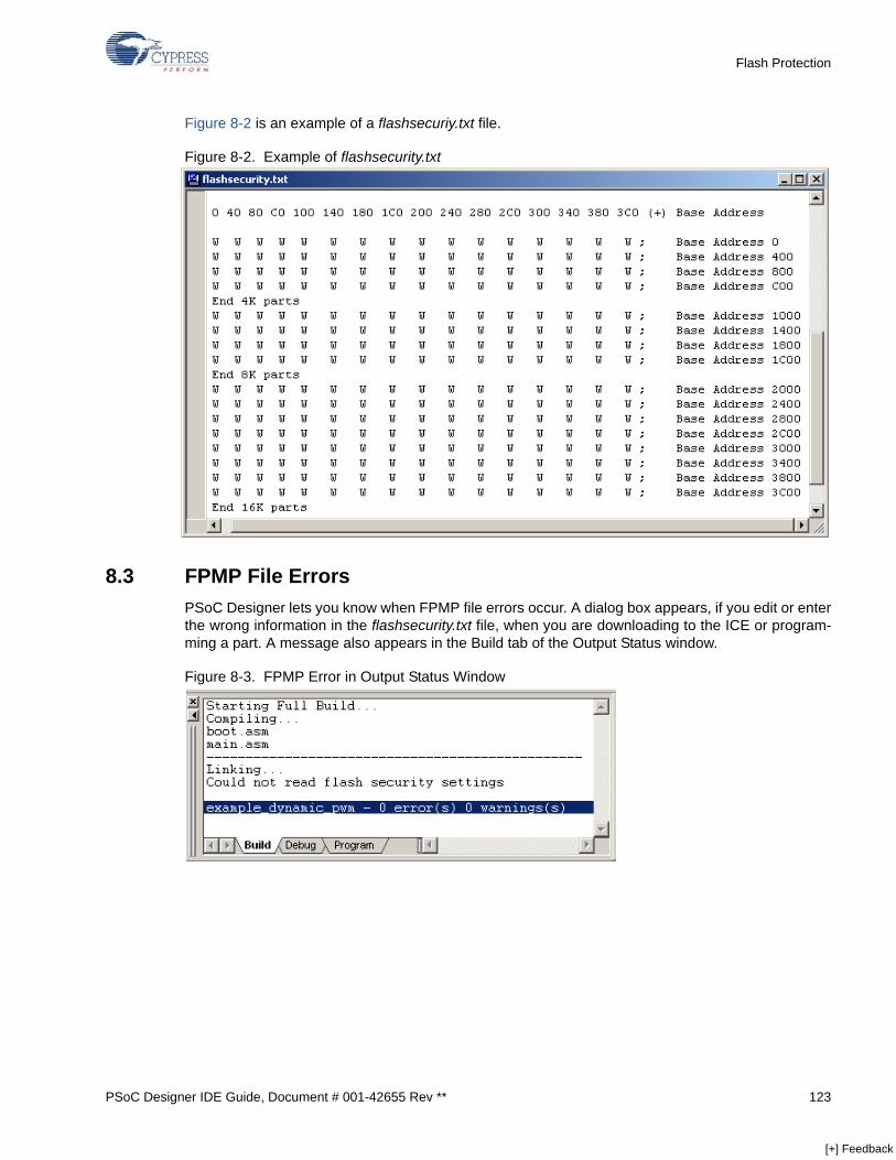
PSoC Designer IDE Guide, Document # 001-42655 Rev ** 123
Flash Protection
Figure 8-2 is an example of a flashsecuriy.txt file.
Figure 8-2. Example of flashsecurity.txt
8.3 FPMP File ErrorsPSoC Designer lets you know when FPMP file errors occur. A dialog box appears, if you edit or enterthe wrong information in the flashsecurity.txt file, when you are downloading to the ICE or program-ming a part. A message also appears in the Build tab of the Output Status window.
Figure 8-3. FPMP Error in Output Status Window
[+] Feedback

124 PSoC Designer IDE Guide, Document # 001-42655 Rev **
Flash Protection
For example, if you have a Flash data table that can be changed using a Flash write routine, youmight have assembly code that looks like this:area Table (ROM, ABS)org 3C80hwidgetTable:export WidgetTabledb 57h ; Wdb 49h ; Idb 44h ; Ddb 47h ; Gdb 45h ; Edb 54h ; T; …. More table entries continue
You then unprotect the Flash block associated with this table at address 3C80h and make yourchange in the flashsecurity.txt file as shown in Figure 8-4.
Figure 8-4. Unprotected Flash at 3C80h
[+] Feedback

PSoC Designer IDE Guide, Document # 001-42655 Rev ** 125
Appendix A. Troubleshooting
This appendix presents solutions for some potential system problems.
A.1 Troubleshooting the Chip-Level EditorProblem: You cannot read the fine print in the User Interface that shows the interconnect
view.
Solution: Place the cursor in the center of the diagram. Right-click the mouse and selectZoom In from the menu. You can also hold the CTRL key and click the image itself
Figure 1-1. Reading the Fine Print
To move the image to a different location on the screen, hold down the ALT key,click in the image with the mouse and drag the image to a place where you want iton the screen.
To zoom out, hold down the CTRL+SHIFT keys and click.
[+] Feedback

126 PSoC Designer IDE Guide, Document # 001-42655 Rev **
A.2 Troubleshooting the Code EditorProblem: You cannot see the Output tab in the Project window.
Solution: From the View menu select Output.
Problem: When building the project, you see this error message: “process_begin: Cre-ateProcess((null), C:\DOCUME~1\bok\LOCALS~1\Temp\make81222.bat, ...)failed make (e=2): The system cannot find the file specified.”.
Solution: Rebuild the project, making certain that no other instances of PSoC Designer arebuilding at the same time.
Problem: When compiling, you see this warning: “!W warning: area ‘<project_name>’ notdefined in startup file './obj/boot.o' and does not have an link time address.”
Solution: This is a bug in PD4.2, see the release notes for more details.
[+] Feedback

PSoC Designer IDE Guide, Document # 001-42655 Rev ** 127
A.3 Troubleshooting the DebuggerProblem: User cannot connect to a pod.
Solution: There are a few possible issues that may cause this problem. One way to beginthe solution process is to create a decision tree that lists the issue and presentspotential causes.
Problem: While debugging, you see the message “Invalid Memory Reference.”
Solution: Similar to previous solution.
Problem: User cannot connect to ICE.
Solution: Similar to the previous solution.
A.4 ICE ConfigurationProblem: It is possible to incorrectly configure the ICE for use with a POD in PSoC
Designer, even though the settings appear to be correct in a certain location.
Solution: There are two places in PSoC designer to adjust Programmer/Emulator settings:
Go into Tools > Options > Debugger tab and uncheck Use default ICE connectionfor all projects.
Go into Project > Settings > Debugger tab, select the ICE from the pull downmenu, Select OK for ICE to power pod and in Power supply voltage, select 3.3v.
A.5 Incorrect Code CompilationProblem: Code does not compile correctly after “*** Warning: File has modification time in
the future” is received. The application is built and a warning: “*** Warning: File has modification time inthe future” is generated at compile time. Any code changes are not updated in thefinal build and not executed at run time.
Cause The compiler checks to see if the source file is newer than the output file beforeregenerating the output file. If the output file is sent to you from a time zone that isseveral hours ahead, then the output file is newer than the source file that you justmodified. Therefore, the source file is not compiled.
Solution: Use the “rebuild all” function to delete all of the output files and regenerate themusing the existing code.
[+] Feedback

128 PSoC Designer IDE Guide, Document # 001-42655 Rev **
A.6 I2C Hot SwappingProblem: The PSoC does not function independently as a hot swap controller with I2C.
The protection diodes on the GPIO pins attached to the I2C bus load the bus if thePSoC Vdd is separate from the I2C power supply and is powered down.
Solution: We have a workaround fix. Please find attached block in PDF format.
Figure 1-2. I2C Hot Swapping
Notes:
Place the N channel FETs used in this block so that the source of the FETsattaches to the PSoC GPIO pin (otherwise the body diodes in the FETs will con-duct in the same way as the protection diodes).
This drawing illustrates the BSS145 from Infineon, but you may select somethingless expensive as long as they are N ch FETs with an RdsON rating for Vgs <=PSoC Vdd. For example, if PSoC Vdd = 3.5V you need an NCH FET with a spec-ified Rds ON for a Vgs <= 3.5V (such as the BSS145).
Setting “Pin X” drive mode to “strong” and writing a 1 to the pin Drive Registerenables the PSoC on the I2C bus. Write a 0 to the pin drive register to disable theI2C.
A.7 Manually Turning off the Analog Section Problem: For situations where low quiescent current is required, such as sleep, you need to
to shutoff the entire analog section. To completely shut off the analog section ofthe PSoC, manually write to the ARF_CR register. You should read about theARF_CR register, in the Technical Reference Manual (TRM), before changing thisregister.
Solution: To turn off the Analog Section use the following code snippet. ARF_CR &= ~0x03;
Trace is “grayed out” while in debug mode if no breakpoints are set.
A.8 Trace IssuesProblem: Debug > Trace is grayed out in the title menu of PSoC Designer 4.2 SP2 when in
Debug mode if user is running.
Solution: Set a breakpoint or click Break on the toolbar. This activates the selections in thedrop down menu.
BSS145
100k
PSoC
Pin 1_5
Pin 1_7
Pin X (to enable I2C)
BSS145I2C SDA
I2C SCL
SD
G
G
D S
[+] Feedback

PSoC Designer IDE Guide, Document # 001-42655 Rev ** 129
A.9 Using an External USB HubProblem: Use an external USB hub to program your PSoC TWICE as fast.
The time it takes to program a PSoC is often reduced when the PSoC is con-nected to an external USB hub. This is because of the Intel chipset based USBfound on many computers.
There are three common USB hub systems: UHCI, OHCI, and EHCI. UHCI andOHCI were developed for the original USB 1.1 spec. UHCI was designed by Inteland is a bare-bones implementation. OHCI is more aggressive and is more widelyused. OHCI is much more efficient and attempts to make better use of the band-width. UHCI merely adheres to the basic specification. EHCI is designed for the2.0 (high speed specification) used to communicate to all high-speed devices.
Solution: External 2.0 Hubs operate very aggressively, like the old OHCI interface. Mostexternal Hubs are much more complex than internal Intel chipset based hubs, andmake much better use of the available bandwidth. If you have a computer with theIntel USB chipset, connecting a 2.0 hub between your PC and your deviceincreases the data transfer rate. Programming the PSoC is usually TWICE as fast!
This speed increase carries over to other applications as well. The amount ofspeed increase depends upon the driver used by the Host PC and the type ofUSB transmission (bulk, isochronous, etc.).
A.10 POD Detection ProblemProblem: While in PSoC Designer you see this error message: Cannot detect a pod.
Solution: 1. Check all connections. Make certain that the ICE is powered and is connectedto the computer.
2. Make sure the ICE driver is correctly installed. Try uninstalling it and reinstallingit.
3. Make sure you are using the correct POD for the part selected in PSoCDesigner. A CY8C29000 POD only emulates CY8C29x parts.
4. Check your PSoC Designer options. There are two places in PSoC Designer toadjust Programmer/Emulator settings:Select Tools > Options > Debugger tab and uncheck Use default ICE connectionfor all projects”.
Select Project > Debugger, select the ICE from the drop down menu, click OK forICE to power pod radio button and under Power supply voltage, click 3.3v.
5. Start a TightLink Case about the issue. Include as many details about theproject and hardware setup as possible. You may have defective hardware.
[+] Feedback

130 PSoC Designer IDE Guide, Document # 001-42655 Rev **
A.11 Project Cloning WarningsProblem: You clone a project and receive what seem to be strange errors or warnings.
Solution: To convert your project between device types, select Start New Project. Thenselect Clone a Configuration and type a name for your new project. In the exist-ing configuration window, select the project to clone and the new device type intowhich to migrate your project. Select Finish. The new version of your project mayrequire modification if you migrated to a part with fewer resources.
Unfortunately, this migration tool does not always migrate the boot.tpl file cor-rectly.
To fix this issue delete the boot.tpl and boot.asm file from the project directory andrestart PSoC Designer. This forces PSoC Designer to regenerate the boot.tpl file.
A.12 AreaName Not DefinedProblem: Warning: area 'AreaName’ not defined in startup file ./obj/boot.o and does
not have an link time address.” applies to assembly code as well.
C compiler generates extraneous warning message relating to RAM AREAS.
In projects that make use of RAM AREAs that are not explicitly defined in theboot.asm, the linker may generate the warning message “Warning: area 'AreaN-ame? not defined in startup file './obj/boot.o' and does not have an link timeaddress.
Solution: You may ignore this message. The warning my also safely be ignored in projectsthat only use assembler.
A.13 General Troubleshooting IssuesProblem: You undocked a minibar, and then closed it by clicking the ‘x’ on the upper right
corner. Now, you cannot get the minibar back.
Solution: From the menu select Tools > Options > Toolbars tab. Select the minibars to dis-play. This restores the closed minibar.
Figure 1-3. Toolbar OPtions Menu
[+] Feedback

PSoC Designer IDE Guide, Document # 001-42655 Rev ** 131
Problem: You have minibars stacked on the left side of the screen pushing down the view-able screen area.
Solution: Increase size of the window and move minibars to the desired location. Thenswitch to another PSoC Designer state to memorize the layout of the currentstate. Repeat this process for the Chip-Level Editor, the Code Editor, and theDebugger because PSoC Designer memorizes their layouts independently.
[+] Feedback

132 PSoC Designer IDE Guide, Document # 001-42655 Rev **
[+] Feedback

PSoC Designer IDE Guide, Document # 001-42655 Rev ** 133
Appendix B. Build Process
This appendix describes the build utilities and process and provides examples for PSoC Designer.
B.1 Build UtilitiesThe build utilities are single-purpose applications that contribute to the build process. Table B-1 pre-sents a list of these utilities. These utilities/programs are installed in the Tools folder beneath the rootinstallation of PSoC Designer.
Make and sed are standard tools with documentation in the Documentation/Supporting Doc-uments folder of the PSoC Designer installation directory.
Table B-1. Utilities and ProgramsUtility/Program Developed By Description
iasm8c.exe ImageCraft Assemblericcomm8c.exe ImageCraft Compiler/Assembler/Linker “Engine”iccm8c.exe ImageCraft Compilerilinkm8c.exe ImageCraft Linkerilstm8c.exe ImageCraft Produces a complete program listing (LST)icppw.exe ImageCraft Preprocessor for compilerilibw.exe ImageCraft Librarian works on an archive file (.a)icc.exe CMS Wraps compiler (iccm8c) but validates license
makehex.exe CMS Creates an Intel HEX file from a ROM file and applies security records.
psocmakemake.exe CMS Creates a project-specific make file (Project.mk)
verLst.exe CMS Adds PSoC and ImageCraft version information to the program listing file.
mkdepend.exe CMS Creates a project-specific dependency file (Project.dep)make.exe GNU Make “Engine” version 3.79sed.exe GNU Formatting utility used within the Makefile version 3.02
[+] Feedback

134 PSoC Designer IDE Guide, Document # 001-42655 Rev **
B.2 Make Process
B.2.1 Environment VariablesPATH: Change the path to add the PSoC designer tools directory. Example: PATH=c:\program files\cypress microsystems\psoc designer\tools;%PATH%
DEVICE: The name of the device.Example: DEVICE=CY8C24794
BASEDEVICE: The tools/include subdirectory of the PSoC Designer install directory that con-tains the include files for the DEVICE.Example: BASEDEVICE=CY8C24090
LASTROM: The last location in ROM.Example: LASTROM=0x3fff
B.2.2 MAKE InvocationsPSoC Designer sets the environment variables as indicated above and calls MAKE as follows:make –f <installdir>/tools/makefile clean make PROJNAME=<projectname> -f <installdir>/tools/makefile makemakemake –f <installdir>/tools/makefile dependmake –f <installdir>/tools/makefile
Make invocations are executed from the project root folder.
B.2.3 Build FilesThis section describes the files used by the build process. Except for ‘Makefile’, these files reside inthe local project folder.
B.2.3.1 Makefile
This file is a general-purpose MAKE file for all PSoC projects. Therefore, use care when changingthe actions in this file, because they apply to all PSoC builds. This file is located in the tools folder, offthe main PSoC Designer installation path.
The relevant makefile targets are:
Makemake targetWhen you use the psocmakemake.exe utility, this target produces the project.mk from theproject.SOC file (see Section B.2.3.2 project.mk).
Depend targetThis runs mkdepend.exe with the appropriate arguments to generate include file dependencies.
All targetThis is the default target that compiles, links, and builds.
Clean targetThis removes all object files.
[+] Feedback

PSoC Designer IDE Guide, Document # 001-42655 Rev ** 135
B.2.3.2 project.mk
Project.mk is generated by psocmakemake.exe from environment variables and the project’s .socfile. It is rewritten by the PSoC Designer build process.
This section describes what these symbolic variables are and gives examples of what values theycan have. Figure B-1 shows an example of a project.mk file for the c24 project using a CY8C24423device.
Figure B-1. Example PROJECT.MK file
The section provides a description of each of the symbolic names found in a project.mk file. You canlook at the master make file in an editor and use a text search utility to see how these symbolicnames are used.
PROJNAME – Helps the master make file create the file name for the .hex, .lst, and .map files.
DEVICE – Not actually used by the master make file, but used by the psocmakemake.exe utility toget things out of the device description XML files. This is a shell environment variable that is setbefore running the ‘makemake’ target.
BASEDEVICE – Used to help create the proper path to a device family specific library. This is a shellenvironment variable that is set before running the ‘makemake’ target.
PROJPATH – Helps create a path to link in the project’s user module library (libpsoc.a)
PSOCDIR – Helps form a path to invoke a sub-make target called ‘expanded_lib_prereq’. This isalso used in formulating other paths.
INCLUDE_PATH – PSoC Designer version 4.2 with Service Pack 1 has a limitation to the use of thismake variable in the master make file. The makemake target (psocmakemake.exe process) essen-tially creates only one path for this variable using the PSOCDIR and BASEDEVICE values. The
PROJNAME=c24DEVICE=CY8C24423BASEDEVICE=CY8C24000BPROJPATH=C:/temp/BASEPA~1/c24PSOCDIR=C:/PROGRA~1/CYPRES~1/PSOCDE~1INCLUDE_PATH=C:/PROGRA~1/CYPRES~1/PSOCDE~1/tools/include/CY8C24~1CSRCS=LIBCSRCS=ASMSRCS= main.asmLIBASMSRCS= delsig8_1.asm delsig8_1int.asm psocconfig.asm psocconfigtbl.asmOBJECT_SOURCES= main.asmFILLVALUE=0x30LASTROM=0xfffLASTRAM=0xffCODECOMPRESSOR=MORE_CFLAGS=-Wf-Osize RELSTART=0x150CDEFINES=LIBS=LIB_PATH=ENABLE_ALIGN_SHIFT=0LMM=SYS_INC_CONTENTS:=SYSTEM_STACK_PAGE:_equ_...etc… SYSTEM_TOOLS=1CONFIG_NAMES=c24
[+] Feedback

136 PSoC Designer IDE Guide, Document # 001-42655 Rev **
master make file also statically adds an include paths to ./lib and %PSOCDIR%/tools/include. How-ever, assume a project had a local.mk file that wanted to add additional include paths to commonfolders that where located away from the project folder using a statement like:
INCLUDE_PATH:=$(INCLUDE_PATH);../common
The assignment, in the master make file, to CY_INCLUDE_PATH receives the potential list ofinclude folders. A list of include paths breaks the path creation that forms variables that produce thememory.inc file. The solution is to modify the master make file assignment to:
CXY_INCLUDE_PATH=$(subst ;, ,$(INCLUDE_PATH))CY_INCLUDE_PATH=$(firstword $(CXY_INCLUDE_PATH))
Notice that in the INCLUDE_PATH example for the local.mk file you must use a colon/equals tobreak any recursion. Also, notice that the include paths are separated by a colon. This colon isreplaced in the master make file by a –I.
CSRCS – This is a (white space separated) list of C files in the root folder of the project. This list isprovided as an argument to the ‘depend’ target (mkdepends.exe process). The master make file wasnot designed to add source files outside of the project directory structure.
LIBCSRCS – This is not used since the master make file is not yet made to ‘compile’ C library files.
ASMSRCS – This is a (white space separated) list of assembly files in the root folder of the project.
LIBASMSRCS – This is a list of project assembly files in the ‘lib’ folder of the project. These files areadded to the project by the Chip-Level Editor and are stored in the project SOC file, which the ‘make-make’ target (psocmakemake.exe process) extracts.
OBJECT_SOURCES – This variable basically governs the link order. The ‘makemake’ target putsthe files in alphabetical order. However, if you wish to change the link order you can revise the orderof the file list assigned to this variable. See Section B.4.4 Change Link Order on page 140 for anexample.
FILLVALUE – This variable is used as a linker argument (e.g. –F0x30) to fill empty areas betweencode and by the MakeHex.exe utility to fill HEX records from the last code record to the end ofFLASH with the fill character. A halt (e.g. 0x30) opcode is used.
LASTROM – This is the FLASH size of the device. It is a shell environment variable that is set beforerunning the ‘makemake’ target. It is used in the link process of the master make file.
LASTRAM – This variable comes from the opts.txt file and gives the last RAM address. The PSoCDesigner build system “asks” the Chip-Level Editor for this value. This value is not really used in themaster make file because most devices that do not have paged RAM are 256 bytes. For examplethis value is 0x7FF for a 2K RAM device and 0xFF for a 256 byte device.
LAST_DATARAM – This variable only shows up in the project.mk file when the project has multiplepages of RAM and paging is enabled. The value is equal to the address of the last RAM byte thatcould be used for data, just before the stack. This value relates to the Stack Page Offset GUI in theCompiler settings of PSoC Designer. For example, if you have a stack page offset of zero (0), withthe stack on Page 7, your LAST_DATARAM value is 0x6FF. For example, with a stack page offset of0x20 (stack on page 7) you get a value, for this variable, of 0x71F.
[+] Feedback

PSoC Designer IDE Guide, Document # 001-42655 Rev ** 137
CODECOMPRESSOR – This is used by the linker in the master make file. PSoC Designer’sProject > Settings Compiler GUI shows two options for the Code Compression Technologies:(1) Condensation and (2) Sublimation. These GUI options are only shown for non-RAM-pageddevice projects. Using the shell environment does not limit you to use these options:
-O: Condensation (or duplicate code removal)-elim: UserModules: Sublimation (unused User Module API elimination)
For example:
CODECOMPRESSOR=-O -elim:UserModules
MORE_CFLAGS – This variable adds ImageCraft commands when compiling C files. The PSoCDesigner ImageCraft compiler settings will hide or allow certain settings based on the project device.For example, for a device that does not have a hardware Multiplier/Accumulator (MAC) the value inMORE_CFLAGS is set to ‘-Wf-nomac’.
-Wf-nomac: Does not generate code to use the MAC.
-Wf-Osize: Uses calls to math library functions instead of inlining the code.
-Wf-LMM8: Tells the compiler to generate paged RAM code for eight pages.
-D_LMM: Needed for C code using >1 page of RAM.
-g -e -c: These are always used by the master make file. They are, respectively, adddebug information, accept C++ comments, and compile file only.
RELSTART – This is the relocatable start address, for example 0x140. This is the starting addressfor the text area (above the TOP area).
CDEFINES – This is added to a command line for compiling C source files. ‘Defines’ are prefixedwith a ‘-D’ and un-defines are prefixed with a ‘-U’. For example:
CDEFINES=-DSET_SPI –DMAX=2 –UADD_DBG
LIBS – This is a list of object (.o) and library (.a) files that you wish to link in from outside the project.The elements must be separated by white space.
LIB_PATH – These are folder locations that should hold the LIBS. Elements in this list should beseparated by semicolons (;). Short (e.g., 8.3) path names should be used.
ENABLE_ALIGN_SHIFT – This is not used.
LMM – This helps the master make file when a project wishes to use paged RAM. The values are a1 or nothing.
SYS_INC_CONTENTS – The value (e.g., list) for this variable is quite long. This value is a mecha-nism used by PSoC Designer to push information about memory settings into an include file that themaster make file creates. Possibly, the additional elements in this list could be added so that you canput your ‘equates’ in the memory include file. The master make file effectively creates the memoryinclude file by redirecting memhead.tpl from the proper device include folder to the top of the mem-ory include file. Then each element in this list is placed in the memory include file after replacing‘_equ_’ with ‘ equ ‘ (spaces added where underscores were). The remainder of the memory includefile comes from the redirection of the memfoot.tpl file (in the proper devices include folder). Again,reading the master make file and understanding this will help a lot.
SYSTEM_TOOLS – This value is 1 for ImageCraft.
CONFIG_NAMES – This lists (white space separated) the overlay (or configuration) names createdin the device editor. This helps the master make file create linker switches to ensure that the RAMdata declared in User Modules gets located on the same RAM page for each overlay.
[+] Feedback

138 PSoC Designer IDE Guide, Document # 001-42655 Rev **
B.2.3.3 Local.mk
This file contains additional make instructions. It is not touched by the make process. Here you canadd and/or modify the build variables set in project.mk.
B.2.3.4 project.dep
Created by the ‘mkdepend’ via the make depend command. This file contains the include dependen-cies for the project. It is rewritten by the build process.
B.2.3.5 local.dep
This file contains additional file dependencies and make commands. It is not touched by the makeprocess.
Since this is the last thing in the make file, assignments here override those in the main make file.See B.4.2 Boot Loader Example on page 139.
B.2.3.6 custom.lkp
This is a ‘legacy’ file inserted via sed into the linker arguments. This is typically used to locate ‘areas’with the -b switch (for example: -bfoo:0x1C00.0x1FFF)
B.2.3.7 opts.txt
This is a file created by PSoC Designer to take the GUI settings for the compiler and linker andtranslate them to ImageCraft arguments and other MAKE variables used by the master make file.The contents of this file gets pulled into the project.mk file
B.3 Moving the Build System to Another PCTypically when there is an interest in using the shell build environment it is because you wish to cre-ate a PSoC HEX file with a minimum build environment on another workstation.
Archive or move the tools folder and all its subfolders. This ensures the same compiler version/release and the same include and library files.
B.3.1 ImageCraft License keyIf you are using C source files then you want to make sure that the workstation you intend to compilefiles on has a valid compiler license. The utility program icc.exe is a wrapper for the ImageCraft com-piler. This wrapper validates the compiler license stored in the registry. The wrapper looks for thecompiler license in this registry key:HKEY_LOCAL_MACHINE\SOFTWARE\Cypress MicroSystems\PSoC Designer\AddIn\Compilers\IMAGECRAFT
There should be a String value (REG_SZ) in this key named COMPILER_LICENSE. Its values areyour license (case sensitive). Create this key by exporting the key and then importing it onto anotherPC or add it manually. This registry key location changed in PSoC Designer version 4.2 (icc.exe).Earlier versions of icc.exe look for the license in the ‘AddIn’ key.
You then need to put your PSoC project files in a folder on the other PC. When you build your projecton the other machine make sure that the PSOCDIR variable, as well as other path-related variables(e.g. INCLUDE_PATH), in a project.mk or local.mk file, point to the appropriate paths.
[+] Feedback

PSoC Designer IDE Guide, Document # 001-42655 Rev ** 139
B.4 Examples
B.4.1 Batch Build FileThis is a .bat file that builds a project; here PSoC Designer is installed in c:\a\pd
set PSOCTOOLS=c:\a\pd\toolsset PATH=%PSOCTOOLS%;c:\winnt\system32;c:\winntset DEVICE=CY8C24423Bset BASEDEVICE=CY8C24000Bset LASTROM=0xFFFmake -f %PSOCTOOLS%\Makefile cleanmake PROJNAME=aa -f %PSOCTOOLS%\Makefile makemakemake –f %PSOCTOOLS%\Makefile dependmake -f %PSOCTOOLS%\Makefile
B.4.2 Boot Loader ExampleThis ‘make’ trick allows a project to have a block of RAM that is shared between a boot-loader andthe boot-loaded code. This trick tells the linker to begin RAM allocation at some point other thanlocation 0. In this example we will have this RAM scratch pad area from RAM address 0 to 4.
In the project's local.mk file add a ‘new’ MAKE variable as follows:STARTRAM:=0x5
In the project’s local.dep file add this line:DATARAM:=-bdata:$(STARTRAM).0xFF
Now in your boot loader code use an absolute RAM area to declare variables in this ‘hidden/shared’area like:
AREA Foo(RAM,ABS)ORG 0export _Z1, _Z2, _Z3, _Z4_Z1: blk 1_Z2: blk 1_Z3: blk 1_Z4: blk 2
[+] Feedback

140 PSoC Designer IDE Guide, Document # 001-42655 Rev **
B.4.3 Add External Files to the ProjectThis is a trick for local.mk to have a ‘custom’ rule to build/add files outside of the project folder.
# CSRCS is used by makedepends to get the external headers/dependenciesCSRCS:=$(CSRCS) ../common/foo.cOBJECT_SOURCES:=$(OBJECT_SOURCES) foo.c# new rule to tell MAKE to get C files from ../common# DON'T have files in COMMON with the same name as this project's Source # Files because we won't know which file MAKE will build last.
obj/%.o : ../common/%.cifeq ($(ECHO_COMMANDS),novice) echo $(call correct_path,$<)endif
$(CCMD) $(CFLAGS) $(CDEFINES) $(INCLUDEFLAGS) $(DEFAULTCFLAGS) -o $@ $(call correct_path,$<)
B.4.4 Change Link Order# The CSRCS and ASMSRCS lists are found in project.mk.# project.mk is generated by psocmakemake.exe and reflects# the project settings (e.g. files, linker options, part family)
# Alter the filter patterns to change the # link order.
C_MY_SORT=$(filter s%.c, $(CSRCS))C_MY_SORT+=$(filter m%.c, $(CSRCS))C_THE_REST= $(filter-out $(C_MY_SORT), $(CSRCS))C_ORDER =$(C_MY_SORT) $(C_THE_REST)
ASM_MY_SORT=$(filter j%.asm, $(ASMSRCS))ASM_MY_SORT+=$(filter h%.asm, $(ASMSRCS))ASM_THE_REST=$(filter-out $(ASM_MY_SORT), $(ASMSRCS))ASM_ORDER=$(ASM_MY_SORT) $(ASM_THE_REST)
OBJECT_SOURCES=$(C_ORDER) $(ASM_ORDER)
# Note: Changes/edits to this file will not re-link# the project since this file is not a prerequisite # condition for the Link 'target'.
[+] Feedback

PSoC Designer IDE Guide, Document # 001-42655 Rev ** 1
Index
Aaddress spaces 94addressing modes 94analog input connection 36analog section, manually turning off
troubleshooting 128application editor
adding existing files 91adding new files 91additional generated files 88file definitions and recommendations 85modifying files 90removing files 91searching files 92troubleshooting 126working in 90
application files, generating 44application programming interfaces 46AreaName not defined, troubleshooting 130assembler
accessing 93address spaces 94addressing modes 94clean compile/assemble/build 98compiling/assembling files 97destination of instruction results 95directives 96file syntax 95instruction format 94instruction set 97list file format 95microprocessor (MCU) 93
assembling and compiling files 97assembly functions, calling from C 98
Bbackup folder for projects 25bank register 0 and 1 window 112boot.asm file
about 45code generation 54in application editor 88
breakpoints 111build utilities 133builder
building a project 101C compiler 102library source 103
linker/loader 102
CC compiler 102code generation 53
active configurations display 55boot.asm 54IO register labels 55limitations 55PSoCConfigTBL.asm 54PSoCDynamic files 55
compatibility with existing projects 19compiler
C compiler 102compiling and assembling files 97components of the debugger 105configuring events, debugger 114connecting user modules 26–32connection to global input 32connection to global output 35CPU register window 112creating
a project directory 17customizing linker actions 103
Ddebugger
breakpoints 111components 105configuring events 114connecting to the ICE 107CPU register window 112debug strategies 109development kit 105downloading to pod 108dynamic event points 114event examples 116flash memory window 112header to device pin connections 120local watch variables 113menu options 106programming the part 119RAM memory window 112registers 0 and 1 window 112trace 110trace log entries 111troubleshooting 127
[+] Feedback

2 PSoC Designer IDE Guide, Document # 001-42655 Rev **
Index
typical event uses 115watch variables 113
default input connection 36design rule checker 43
running 43development kit 105device editor
interrupt vectors 48troubleshooting 125
digital interconnect row input window 32dynamic event points 114dynamic reconfiguration
add configurations 50application editor 53code generation 53delete configurations 51global parameters 52port pin settings 52rename configurations 52
Eevent examples
find memory write 116register A value, trace on and off, and match
count 117stack overflow 116
Ffile definitions and recommendations in application
editor 85file errors in FPMP 123file syntax 95file types and extensions 86flash memory window 112flash program memory protection
file errors 123flashsecurity.txt file 122options 121
flashsecurity.txt file 121, 122
Ggeneral troubleshooting issues 130generating application files 44–45global resources 22–25global variables 113Globalparams.h file 89globalparams.inc file 89
Hheaders and library header folders 87hot swapping, I2C troubleshooting 128
II2C hot swapping, troubleshooting 128ICE
connecting to PC 107troubleshooting 127
ICE, connecting to 107icons
generate application 44interconnect view 26next allowed placement 20options for modifying files 90place user module 20restore default pinout 35undo place user module 20
incorrect code compilation, troubleshooting 127instruction format 94instruction set notation 97interconnections
analog clock select 27analog column clock 28analog column input mux 29analog column input select 29analog output buffer 29comparator analog LUT 32connection to global input 32connection to global output 35CT analog block RBotMux 31digital block clock input 30digital block output 31digital interconnect row input window 32digital interconnect row output window 33enable digital block input 30global in 26global out 27row broadcast 31row logic table input 33row logic table select 34selection of ACMux, BMux, AnalogBus and CompBus
for SC analog block 31selection of NMux, PMux, AnalogBus and CompBus
for CT analog block 31synchronization 33
interconnectivity in user modules 25interrupt service routines, ISRs 46interrupt vectors in device editor 48interrupts, port 41ISRs ??–47
Llib (librarian) file folder 86library headers 103library source 86, 103library source folder 87linker/loader 102list file format 95
Mmain.asm file 88
[+] Feedback

PSoC Designer IDE Guide, Document # 001-42655 Rev ** 3
Index
main.c file 88make process 134make utility 97menu options in the debugger 106microprocessor (MCU) 93
Nname user modules 20
Oobj (objects) file folder 86options for modifying source files 90output file folder 86output tab 87
Pparameters, user modules 21parts catalog 18pinout specification 35placing user modules 19–??POD detection, troubleshooting 129port connections
analog input 36analog output buffer 36default input 36Ext Ref 39ExternalGND 39Global_IN_x 37Global_OUT_x 37I2C SDA 40StdCPU 38XtalIn 38XtalOut 38
port drive modes 40port interrupts
ChangeFromRead 41DisableInt 41FallingEdge 42RisingEdge 42
programming parts in debugger 119project
backup folder 25building 101file system 87
project cloning warnings, troubleshooting 130PSoC dynamic files 55PSoCConfig.asm file 53
in application editor 88PSoCConfigTBL.asm file 54PSoCgpioint.h file 89PSoCgpioint.inc file 88
RRAM memory window 112
registersinternal 93
removing user modules 21rename user modules 20resource manager 19resource meter 42rotating user modules 21row logic table input 33row logic table select 34
Sshadow registers 88source files folder 87source files generated by generate application
operation 45source tree 87stack overflow, event examples 116system interface 86system supervisor call 121
Ttrace issues, troubleshooting 128trace window 110tracking device space 42troubleshooting
analog section, manually turning off 128application editor 126AreaName not defined 130debugger 127device editor 125general troubleshooting issues 130I2C hot swapping 128ICE configuration 127incorrect code compilation 127POD detection 129project cloning warnings 130trace issues 128USB hub 129
Uupdating user module parameters 21USB hub, troubleshooting 129user modules
deploying interconnectivity 25global resources 22–25name 20placing 19–??removing 21rename 20restore default pinout 35restore global resource defaults 22rotating a placement 21setting parameters 21specifying pinout 35tracking device space 42
[+] Feedback

4 PSoC Designer IDE Guide, Document # 001-42655 Rev **
Index
Vversion control system 87
Wwatch variables
array types 113global 113
working in application editor 90working with ISRs 47write only register shadows 88
[+] Feedback

PSoC Designer IDE Guide, Document # 001-42655 Rev ** 5
Glossary
A)
active windows Subsystem-related windows that are open and workable.
analog PSoC blocks Basic programmable opamp circuits. There are SC (switched capacitor) and CT (con-tinuous time) blocks. These blocks can be interconnected to provide ADCs, DACs,multi-pole filters, gain stages, and much more.
Application Program-ming Interface (API)
A series of software routines that comprise an interface between a computer applica-tion and lower-level services and functions (for example, user modules and libraries).APIs serve as building blocks for programmers that create software applications.
Code Editor PSoC Designer subsystem where users edit and program C Compiler and assemblylanguage source files.
assemble (combined with compiling)
Assembling, in PSoC Designer, translates all relative-addressed code into a single.rom file with absolute addressing.
B
build/link Building your project in PSoC Designer links all the programmed functionality of thesource files and loads it into a .rom file, which is the file you download for debuggingand programming.
C
compile (combined with assembling)
Compiling, in PSoC Designer, takes the most prominent, open file and translates thecode into object source code with relative addresses.
D
debugger A hardware and software system that allows the user to analyze the operation of thesystem under development. A debugger usually allows the developer to step throughthe firmware one step at a time, set break points, and analyze memory.
[+] Feedback

6 PSoC Designer IDE Guide, Document # 001-42655 Rev **
Glossary
design (export/import)
One or more loadable configurations that can be exported from a project then importedand used in a new or existing project. A loadable configuration consists of one or more“placed” user modules with module parameters, Global Resources, set pinouts, andgenerated application files.
design browser Venue to identify reusable designs for import to PSoC Designer projects.
Chip-Level Editor PSoC Designer subsystem where you choose/configure your device.
digital PSoC blocks The 8-bit logic blocks that can act as a counter, timer, serial receiver, serial transmitter,CRC generator, pseudo-random number generator, or SPI.
dynamic reconfigura-tion
Dynamic Reconfiguration allows for applications to dynamically load and unload con-figurations. With this feature, your single PSoC MCU can have multiple functions.
F
family of devices PSoC family of devices consists of several device groups: CY8C21xxx, CY8C22xxx,CY8C24xxx, CY8C25xxx, CY8C26xxx, CY8C27xxx, CY8C29xxx
I
ICE-4000 The in-circuit emulator that allows users to test the project in a hardware environment,while viewing the debugging device activity in a software environment (PSoCDesigner).
ice-Cube In-Circuit Emulator (ICE) that replaces the ICE-4000 and USB adapter for seamlessUSB connection, debugging, and programming.
interrupt service rou-tine (ISR)
A block of code that normal code execution is diverted to when the M8C receives ahardware interrupt. Many interrupt sources may each exist with its own priority andindividual ISR code block. Each ISR code block ends with the RETI instruction, return-ing the device to the point in the program where it left normal program execution.
L
link/build Linking your project in PSoC Designer links all programmed functionality of the sourcefiles (with absolute addressing) and loads it into a .rom file, which is the file you down-load for debugging and programming.
M
M8C An 8-bit Harvard Architecture microprocessor. The microprocessor coordinates allactivity inside a PSoC by interfacing to the Flash, SRAM, and register space.
[+] Feedback

PSoC Designer IDE Guide, Document # 001-42655 Rev ** 7
Glossary
miniProg1 Developmental programmer that provides a low-cost solution for learning about, pro-gramming and evaluating the PSoC.
P
pod Part of the ICE that emulates functionality, in which debugging occurs.
PSoC Cypress MicroSystems’ Programmable System-on-Chip (PSoC) mixed signal array.PSoC™ and Programmable System-on-Chip™ are trademarks of Cypress MicroSys-tems, Inc.
PSoCEval1 Evaluation board that provides a low-cost solution for learning about, programming,and evaluating the PSoC.
PSoC blocks See analog blocks and digital blocks.
PSoC Designer The software for Cypress MicroSystems’ Programmable System-on-Chip technology.
PSoC Programmer New, multi-functional programming software accessible from within PSoC Designer.
S
source tree Project file system displayed by default in left frame of Workspace Explorer.
subsystem PSoC Designer has three subsystems: Chip-Level Editor, Code Editor, and Debugger.
U
USB adapter Port connection to work the ICE in PSoC Designer v. 4.1 or later.
user modules Accessible, preconfigured function that, once placed and programmed, will work as aperipheral in the target device.
[+] Feedback

8 PSoC Designer IDE Guide, Document # 001-42655 Rev **
Glossary
[+] Feedback