Embed Size (px)
Citation preview
www.cypress.com Document No. 001-72382 Rev. *E 1
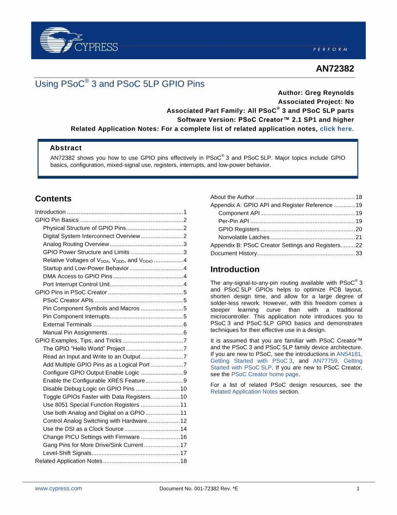
AN72382
Using PSoC® 3 and PSoC 5LP GPIO Pins Author: Greg Reynolds
Associated Project: No
Associated Part Family: All PSoC® 3 and PSoC 5LP parts
Software Version: PSoC Creator™ 2.1 SP1 and higher
Related Application Notes: For a complete list of related application notes, click here.
Abstract
AN72382 shows you how to use GPIO pins effectively in PSoC® 3 and PSoC 5LP. Major topics include GPIO
basics, configuration, mixed-signal use, registers, interrupts, and low-power behavior.
Contents
Introduction ....................................................................... 1 GPIO Pin Basics ............................................................... 2
Physical Structure of GPIO Pins ................................... 2 Digital System Interconnect Overview .......................... 2 Analog Routing Overview ............................................. 3 GPIO Power Structure and Limits ................................ 3 Relative Voltages of VDDA, VDDD, and VDDIO .................. 4 Startup and Low-Power Behavior ................................. 4 DMA Access to GPIO Pins ........................................... 4 Port Interrupt Control Unit............................................. 4
GPIO Pins in PSoC Creator .............................................. 5 PSoC Creator APIs ...................................................... 5 Pin Component Symbols and Macros .......................... 5 Pin Component Interrupts............................................. 5 External Terminals ....................................................... 6 Manual Pin Assignments .............................................. 6
GPIO Examples, Tips, and Tricks ..................................... 7 The GPIO ―Hello World‖ Project ................................... 7 Read an Input and Write to an Output .......................... 7 Add Multiple GPIO Pins as a Logical Port .................... 7 Configure GPIO Output Enable Logic .......................... 9 Enable the Configurable XRES Feature ....................... 9 Disable Debug Logic on GPIO Pins ........................... 10 Toggle GPIOs Faster with Data Registers .................. 10 Use 8051 Special Function Registers ........................ 11 Use both Analog and Digital on a GPIO ..................... 11 Control Analog Switching with Hardware.................... 12 Use the DSI as a Clock Source .................................. 14 Change PICU Settings with Firmware ........................ 16 Gang Pins for More Drive/Sink Current ...................... 17 Level-Shift Signals ...................................................... 17
Related Application Notes ............................................... 18
About the Author ............................................................. 18 Appendix A: GPIO API and Register Reference ............. 19
Component API .......................................................... 19 Per-Pin API ................................................................ 19 GPIO Registers .......................................................... 20 Nonvolatile Latches .................................................... 21
Appendix B: PSoC Creator Settings and Registers......... 22 Document History ............................................................ 33
Introduction
The any-signal-to-any-pin routing available with PSoC® 3
and PSoC 5LP GPIOs helps to optimize PCB layout, shorten design time, and allow for a large degree of solder-less rework. However, with this freedom comes a steeper learning curve than with a traditional microcontroller. This application note introduces you to PSoC 3 and PSoC 5LP GPIO basics and demonstrates techniques for their effective use in a design.
It is assumed that you are familiar with PSoC Creator™ and the PSoC 3 and PSoC 5LP family device architecture. If you are new to PSoC, see the introductions in AN54181, Getting Started with PSoC 3, and AN77759, Getting Started with PSoC 5LP. If you are new to PSoC Creator, see the PSoC Creator home page.
For a list of related PSoC design resources, see the Related Application Notes section.
Using PSoC® 3 and PSoC 5LP GPIO Pins
www.cypress.com Document No. 001-72382 Rev. *E 2
GPIO Pin Basics
In PSoC 3 and PSoC 5LP devices, the GPIO, SIO, and USB pins are similar. Unlike GPIO pins, though, the SIO and USB pins have different drive strengths and application-specific features. Some of the GPIO pins also have secondary dedicated functions, such as opamp inputs and outputs, programming and debugging interfaces, or DAC outputs. When they are not being used for special functions, all GPIO pins behave the same. Depending on the package type, PSoC devices can have as many as 62 GPIO pins.
Physical Structure of GPIO Pins
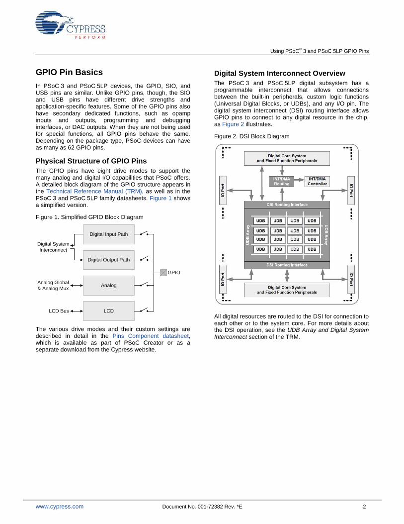
The GPIO pins have eight drive modes to support the many analog and digital I/O capabilities that PSoC offers. A detailed block diagram of the GPIO structure appears in the Technical Reference Manual (TRM), as well as in the PSoC 3 and PSoC 5LP family datasheets. Figure 1 shows a simplified version.
Figure 1. Simplified GPIO Block Diagram
Digital Input Path
Digital Output Path
Analog
LCD
Digital System
Interconnect
Analog Global
& Analog Mux
LCD Bus
GPIO
The various drive modes and their custom settings are described in detail in the Pins Component datasheet, which is available as part of PSoC Creator or as a separate download from the Cypress website.
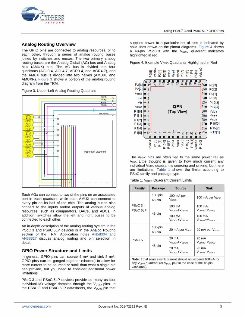
Digital System Interconnect Overview
The PSoC 3 and PSoC 5LP digital subsystem has a programmable interconnect that allows connections between the built-in peripherals, custom logic functions (Universal Digital Blocks, or UDBs), and any I/O pin. The digital system interconnect (DSI) routing interface allows GPIO pins to connect to any digital resource in the chip, as Figure 2 illustrates.
Figure 2. DSI Block Diagram
All digital resources are routed to the DSI for connection to each other or to the system core. For more details about the DSI operation, see the UDB Array and Digital System Interconnect section of the TRM.
Using PSoC® 3 and PSoC 5LP GPIO Pins
www.cypress.com Document No. 001-72382 Rev. *E 3
Analog Routing Overview
The GPIO pins are connected to analog resources, or to each other, through a series of analog routing buses joined by switches and muxes. The two primary analog routing buses are the Analog Global (AG) bus and Analog Mux (AMUX) bus. The AG bus is divided into four quadrants (AGL0-4, AGL4-7, AGR0-4, and AGR4-7), and the AMUX bus is divided into two halves (AMUXL and AMUXR). Figure 3 shows a portion of the analog routing diagram from the TRM.
Figure 3. Upper-Left Analog Routing Quadrant
Each AGx can connect to two of the pins on an associated port in each quadrant, while each AMUX can connect to every pin on its half of the chip. The analog buses also connect to the inputs and/or outputs of various analog resources, such as comparators, DACs, and ADCs. In addition, switches allow the left and right buses to be connected to each other.
An in-depth description of the analog routing system in the PSoC 3 and PSoC 5LP devices is in the Analog Routing section of the TRM. Application notes AN58304 and AN58827 discuss analog routing and pin selection in detail.
GPIO Power Structure and Limits
In general, GPIO pins can source 4 mA and sink 8 mA. GPIO pins can be ganged together (shorted) to allow for more current to be sourced or sunk than what a single pin can provide, but you need to consider additional power limitations.
PSoC 3 and PSoC 5LP devices provide as many as four individual I/O voltage domains through the VDDIO pins. In the PSoC 3 and PSoC 5LP datasheets, the VDDIO pin that
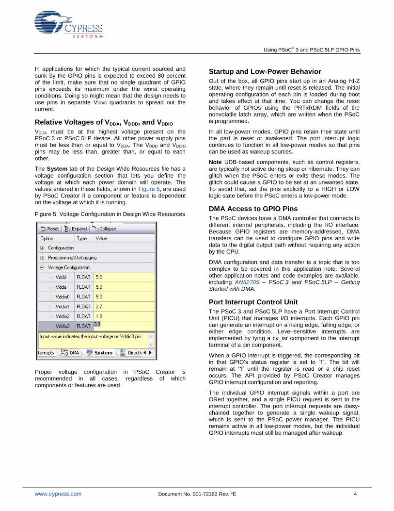
supplies power to a particular set of pins is indicated by solid lines drawn on the pinout diagrams. Figure 4 shows a 48-pin PSoC 3 with the VDDIO quadrant indicators highlighted in red.
Figure 4. Example VDDIO Quadrants Highlighted in Red
The VDDIO pins are often tied to the same power rail as VDD. Little thought is given to how much current any individual VDDIO quadrant is sourcing and sinking, but there are limitations. Table 1 shows the limits according to PSoC family and package type.
Table 1. VDDIO Quadrant Current Limits
Family Package Source Sink
PSoC 3
PSoC 5LP
100-pin
68-pin
100 mA per VDDIO
100 mA per VDDIO
48-pin
100 mA VDDIO0+VDDIO2
100 mA VDDIO1+VDDIO3
100 mA VDDIO0+VDDIO2
100 mA VDDIO1+VDDIO3
PSoC 5
100-pin
68-pin 20 mA per VDDIO 20 mA per VDDIO
48-pin
20 mA VDDIO0+VDDIO2
20 mA VDDIO1+VDDIO3
20 mA VDDIO0+VDDIO2
20 mA VDDIO1+VDDIO3
Note: Total source+sink current should not exceed 100mA for any VDDIO quadrant (or VDDIO pair in the case of the 48-pin packages).
Using PSoC® 3 and PSoC 5LP GPIO Pins
www.cypress.com Document No. 001-72382 Rev. *E 4
In applications for which the typical current sourced and sunk by the GPIO pins is expected to exceed 80 percent of the limit, make sure that no single quadrant of GPIO pins exceeds its maximum under the worst operating conditions. Doing so might mean that the design needs to use pins in separate VDDIO quadrants to spread out the current.
Relative Voltages of VDDA, VDDD, and VDDIO
VDDA must be at the highest voltage present on the PSoC 3 or PSoC 5LP device. All other power supply pins must be less than or equal to VDDA. The VDDD and VDDIO pins may be less than, greater than, or equal to each other.
The System tab of the Design Wide Resources file has a
voltage configuration section that lets you define the voltage at which each power domain will operate. The values entered in these fields, shown in Figure 5, are used by PSoC Creator if a component or feature is dependent on the voltage at which it is running.
Figure 5. Voltage Configuration in Design Wide Resources
Proper voltage configuration in PSoC Creator is recommended in all cases, regardless of which components or features are used.
Startup and Low-Power Behavior
Out of the box, all GPIO pins start up in an Analog HI-Z state, where they remain until reset is released. The initial operating configuration of each pin is loaded during boot and takes effect at that time. You can change the reset behavior of GPIOs using the PRTxRDM fields of the nonvolatile latch array, which are written when the PSoC is programmed.
In all low-power modes, GPIO pins retain their state until the part is reset or awakened. The port interrupt logic continues to function in all low-power modes so that pins can be used as wakeup sources.
Note UDB-based components, such as control registers,
are typically not active during sleep or hibernate. They can glitch when the PSoC enters or exits these modes. The glitch could cause a GPIO to be set at an unwanted state. To avoid that, set the pins explicitly to a HIGH or LOW logic state before the PSoC enters a low-power mode.
DMA Access to GPIO Pins
The PSoC devices have a DMA controller that connects to different internal peripherals, including the I/O interface. Because GPIO registers are memory-addressed, DMA transfers can be used to configure GPIO pins and write data to the digital output path without requiring any action by the CPU.
DMA configuration and data transfer is a topic that is too complex to be covered in this application note. Several other application notes and code examples are available, including AN52705 – PSoC 3 and PSoC 5LP – Getting Started with DMA.
Port Interrupt Control Unit
The PSoC 3 and PSoC 5LP have a Port Interrupt Control Unit (PICU) that manages I/O interrupts. Each GPIO pin can generate an interrupt on a rising edge, falling edge, or either edge condition. Level-sensitive interrupts are implemented by tying a cy_isr component to the interrupt terminal of a pin component.
When a GPIO interrupt is triggered, the corresponding bit in that GPIO‘s status register is set to ‗1‘. The bit will remain at ‗1‘ until the register is read or a chip reset occurs. The API provided by PSoC Creator manages GPIO interrupt configuration and reporting.
The individual GPIO interrupt signals within a port are ORed together, and a single PICU request is sent to the interrupt controller. The port interrupt requests are daisy-chained together to generate a single wakeup signal, which is sent to the PSoC power manager. The PICU remains active in all low-power modes, but the individual GPIO interrupts must still be managed after wakeup.
Using PSoC® 3 and PSoC 5LP GPIO Pins
www.cypress.com Document No. 001-72382 Rev. *E 5
GPIO Pins in PSoC Creator
This section describes how to use PSoC Creator to configure and manipulate GPIO pins. PSoC Creator combines text and graphical editing interfaces so that designers can set their hardware configuration and write firmware at the same time.
PSoC Creator APIs
Cypress provides a set of APIs that you can use to dynamically control GPIOs through firmware. The APIs for the Pins component enable access on both a component-wide and per-pin basis.
The cy_boot component also provides functions to access chip resources. The functions in cy_boot are not part of the individual component libraries, but the libraries can use them. The per-pin APIs, which are provided as part of cy_boot, in the cypins.h file, are documented in the Pins section of the System Reference Guide. You can use these APIs to control the configuration registers for each physical pin.
For a summary and a simple code example for the APIs related to GPIOs, see Appendix A: GPIO API and Register Reference, starting on page 19.
Pin Component Symbols and Macros
The cy_pins component is the recommended way for
internal PSoC resources to connect to a physical pin. It allows PSoC Creator to automatically place and route the signals within the PSoC based on the chosen configuration of the pin. The standard Cypress component catalog contains four types of predefined GPIO configurations (macros) in the Ports and Pins class of symbols—analog, digital bidirectional, digital input, and digital output. Drag one of these component macros to the schematic to add a pin to the project, as Figure 6 shows.
Figure 6. Pin Component Symbol Types in PSoC Creator
You are not confined to one type of pin configuration based on which macro symbol you choose. After you place the pin symbol on the schematic, you can configure its behavior using the component customizer options described later in this document.
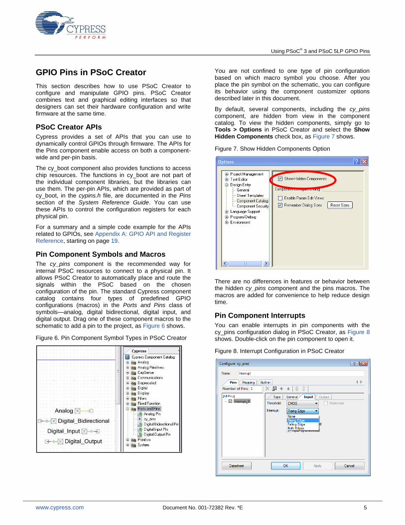
By default, several components, including the cy_pins component, are hidden from view in the component catalog. To view the hidden components, simply go to Tools > Options in PSoC Creator and select the Show Hidden Components check box, as Figure 7 shows.
Figure 7. Show Hidden Components Option
There are no differences in features or behavior between the hidden cy_pins component and the pins macros. The
macros are added for convenience to help reduce design time.
Pin Component Interrupts
You can enable interrupts in pin components with the cy_pins configuration dialog in PSoC Creator, as Figure 8 shows. Double-click on the pin component to open it.
Figure 8. Interrupt Configuration in PSoC Creator
Using PSoC® 3 and PSoC 5LP GPIO Pins
www.cypress.com Document No. 001-72382 Rev. *E 6
The pin component symbol changes when interrupts are enabled, as Figure 9 shows. The irq signal of the pin component will toggle when a pin interrupt is triggered. You do not need to connect the irq terminal to an isr component to enable a pin interrupt.
Figure 9. The Pin Component Symbol Changes with Interrupts Enabled
If interrupts are enabled, you can use only one pin component with each physical GPIO port. The reason for this limitation is that all pin interrupts in a port are ORed together, so only one irq signal can be shown on the schematic.
For example, consider two pin components with interrupts enabled, as Figure 10 shows. These components cannot be mapped to pins in the same physical port because there are now two separate irq signals in the Creator schematic, but there is really only one physical PICU interrupt generated for the entire port.
Figure 10. Two pin components with interrupts.
Creator will give an error if you try to assign these two components to the same port. The accepted method is to assign multiple pins to the same component, as Figure 11 shows. This ensures that there is only one irq signal in the schematic for that physical port. You can still assign each pin its own interrupt edge type. The only limitation is that the pins must be contiguous.
Figure 11. Pin selection with different interrupt edge types.
You can also use the PICUx_INTTYPEy registers to enable or change interrupts on any GPIO pin, regardless of component settings. See the appendices for more information on these registers.
External Terminals
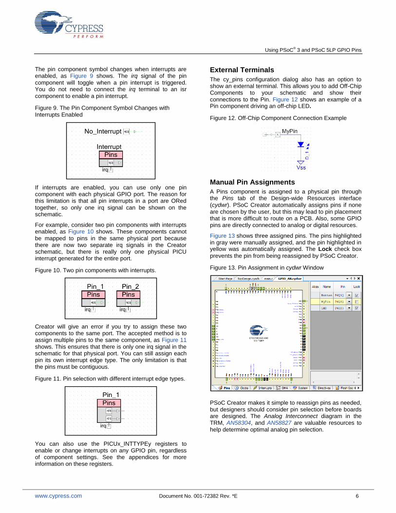
The cy_pins configuration dialog also has an option to show an external terminal. This allows you to add Off-Chip Components to your schematic and show their connections to the Pin. Figure 12 shows an example of a Pin component driving an off-chip LED.
Figure 12. Off-Chip Component Connection Example
Manual Pin Assignments
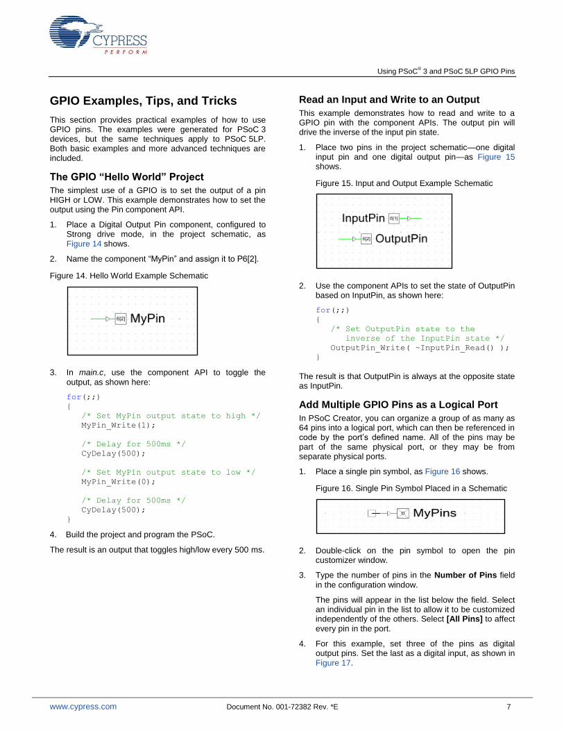
A Pins component is assigned to a physical pin through the Pins tab of the Design-wide Resources interface (cydwr). PSoC Creator automatically assigns pins if none are chosen by the user, but this may lead to pin placement that is more difficult to route on a PCB. Also, some GPIO pins are directly connected to analog or digital resources.
Figure 13 shows three assigned pins. The pins highlighted in gray were manually assigned, and the pin highlighted in yellow was automatically assigned. The Lock check box
prevents the pin from being reassigned by PSoC Creator.
Figure 13. Pin Assignment in cydwr Window
PSoC Creator makes it simple to reassign pins as needed, but designers should consider pin selection before boards are designed. The Analog Interconnect diagram in the TRM, AN58304, and AN58827 are valuable resources to help determine optimal analog pin selection.
Using PSoC® 3 and PSoC 5LP GPIO Pins
www.cypress.com Document No. 001-72382 Rev. *E 7
GPIO Examples, Tips, and Tricks
This section provides practical examples of how to use GPIO pins. The examples were generated for PSoC 3 devices, but the same techniques apply to PSoC 5LP. Both basic examples and more advanced techniques are included.
The GPIO “Hello World” Project
The simplest use of a GPIO is to set the output of a pin HIGH or LOW. This example demonstrates how to set the output using the Pin component API.
1. Place a Digital Output Pin component, configured to Strong drive mode, in the project schematic, as Figure 14 shows.
2. Name the component ―MyPin‖ and assign it to P6[2].
Figure 14. Hello World Example Schematic
3. In main.c, use the component API to toggle the
output, as shown here:
for(;;)
{
/* Set MyPin output state to high */
MyPin_Write(1);
/* Delay for 500ms */
CyDelay(500);
/* Set MyPin output state to low */
MyPin_Write(0);
/* Delay for 500ms */
CyDelay(500);
}
4. Build the project and program the PSoC.
The result is an output that toggles high/low every 500 ms.
Read an Input and Write to an Output
This example demonstrates how to read and write to a GPIO pin with the component APIs. The output pin will drive the inverse of the input pin state.
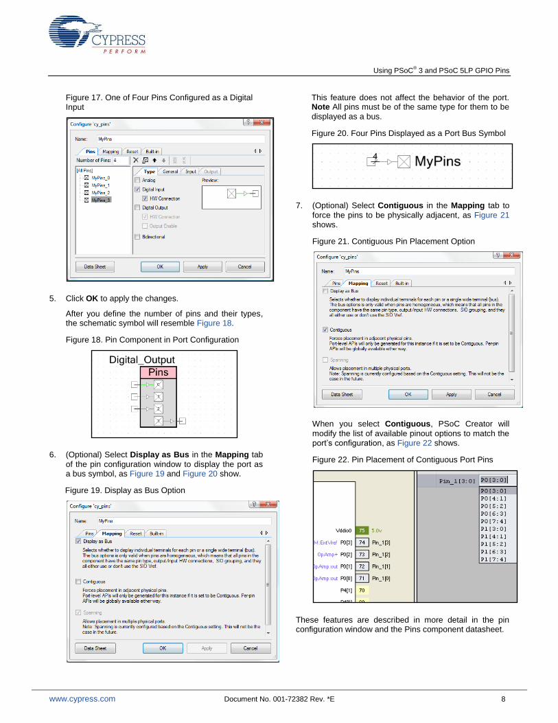
1. Place two pins in the project schematic—one digital input pin and one digital output pin—as Figure 15 shows.
Figure 15. Input and Output Example Schematic
2. Use the component APIs to set the state of OutputPin based on InputPin, as shown here:
for(;;)
{
/* Set OutputPin state to the
inverse of the InputPin state */
OutputPin_Write( ~InputPin_Read() );
}
The result is that OutputPin is always at the opposite state as InputPin.
Add Multiple GPIO Pins as a Logical Port
In PSoC Creator, you can organize a group of as many as 64 pins into a logical port, which can then be referenced in code by the port‘s defined name. All of the pins may be part of the same physical port, or they may be from separate physical ports.
1. Place a single pin symbol, as Figure 16 shows.
Figure 16. Single Pin Symbol Placed in a Schematic
2. Double-click on the pin symbol to open the pin customizer window.
3. Type the number of pins in the Number of Pins field
in the configuration window.
The pins will appear in the list below the field. Select an individual pin in the list to allow it to be customized independently of the others. Select [All Pins] to affect
every pin in the port.
4. For this example, set three of the pins as digital output pins. Set the last as a digital input, as shown in Figure 17.
Using PSoC® 3 and PSoC 5LP GPIO Pins
www.cypress.com Document No. 001-72382 Rev. *E 8
Figure 17. One of Four Pins Configured as a Digital Input
5. Click OK to apply the changes.
After you define the number of pins and their types, the schematic symbol will resemble Figure 18.
Figure 18. Pin Component in Port Configuration
6. (Optional) Select Display as Bus in the Mapping tab
of the pin configuration window to display the port as a bus symbol, as Figure 19 and Figure 20 show.
Figure 19. Display as Bus Option
This feature does not affect the behavior of the port. Note All pins must be of the same type for them to be
displayed as a bus.
Figure 20. Four Pins Displayed as a Port Bus Symbol
7. (Optional) Select Contiguous in the Mapping tab to
force the pins to be physically adjacent, as Figure 21 shows.
Figure 21. Contiguous Pin Placement Option
When you select Contiguous, PSoC Creator will
modify the list of available pinout options to match the port‘s configuration, as Figure 22 shows.
Figure 22. Pin Placement of Contiguous Port Pins
These features are described in more detail in the pin configuration window and the Pins component datasheet.
Using PSoC® 3 and PSoC 5LP GPIO Pins
www.cypress.com Document No. 001-72382 Rev. *E 9
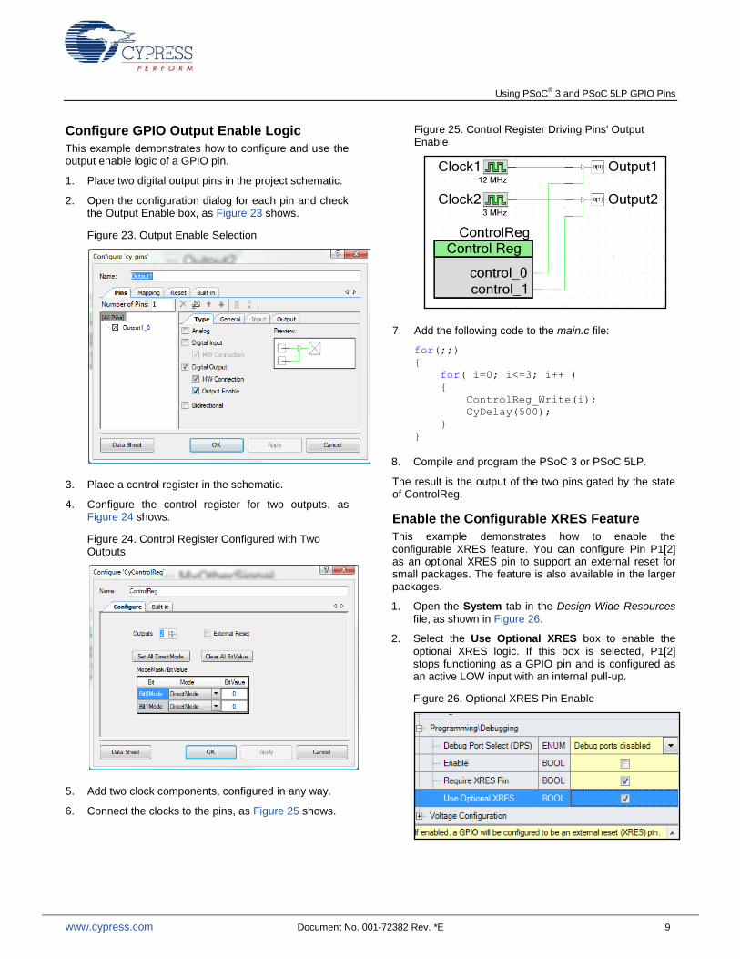
Configure GPIO Output Enable Logic
This example demonstrates how to configure and use the output enable logic of a GPIO pin.
1. Place two digital output pins in the project schematic.
2. Open the configuration dialog for each pin and check the Output Enable box, as Figure 23 shows.
Figure 23. Output Enable Selection
3. Place a control register in the schematic.
4. Configure the control register for two outputs, as Figure 24 shows.
Figure 24. Control Register Configured with Two Outputs
5. Add two clock components, configured in any way.
6. Connect the clocks to the pins, as Figure 25 shows.
Figure 25. Control Register Driving Pins' Output Enable
7. Add the following code to the main.c file:
for(;;)
{
for( i=0; i<=3; i++ )
{
ControlReg_Write(i);
CyDelay(500);
}
}
8. Compile and program the PSoC 3 or PSoC 5LP.
The result is the output of the two pins gated by the state of ControlReg.
Enable the Configurable XRES Feature
This example demonstrates how to enable the configurable XRES feature. You can configure Pin P1[2] as an optional XRES pin to support an external reset for small packages. The feature is also available in the larger packages.
1. Open the System tab in the Design Wide Resources
file, as shown in Figure 26.
2. Select the Use Optional XRES box to enable the
optional XRES logic. If this box is selected, P1[2] stops functioning as a GPIO pin and is configured as an active LOW input with an internal pull-up.
Figure 26. Optional XRES Pin Enable
Using PSoC® 3 and PSoC 5LP GPIO Pins
www.cypress.com Document No. 001-72382 Rev. *E 10
3. Program the PSoC to write the setting to the nonvolatile array. It will take effect after the next power-on.
4. Clear the check box and reprogram the PSoC to restore normal GPIO functionality.
Note that all PSoC 3 and PSoC 5LP devices come from the factory with the optional XRES feature disabled. Using the configurable XRES pin does not change the functionality of a dedicated XRES pin.
Disable Debug Logic on GPIO Pins
This example demonstrates how to disable the debug logic associated with the port 1 pins. If the debug port feature is enabled, the PSoC will enter debug mode if it detects activity on these pins at boot time.
1. Open the Design-wide Resources file and click the System tab.
2. Select Debug ports disabled from the drop-down
menu, as Figure 27 shows.
Figure 27. Debug Port Disabled
3. Compile and program the PSoC 3 or PSoC 5LP.
Note that the debug port must be manually enabled again if debug is needed. Disabling the debug interface does not affect the ability to program the device.
Toggle GPIOs Faster with Data Registers
This example demonstrates how to use port data registers and masks to quickly toggle pins. While the component API is the easiest way to control GPIO pins, the number of processor cycles needed to update the pin can affect how fast a toggle can occur. The register definitions and masks in the <pin_name>.h file that is created for each component can be used to more quickly update pins.
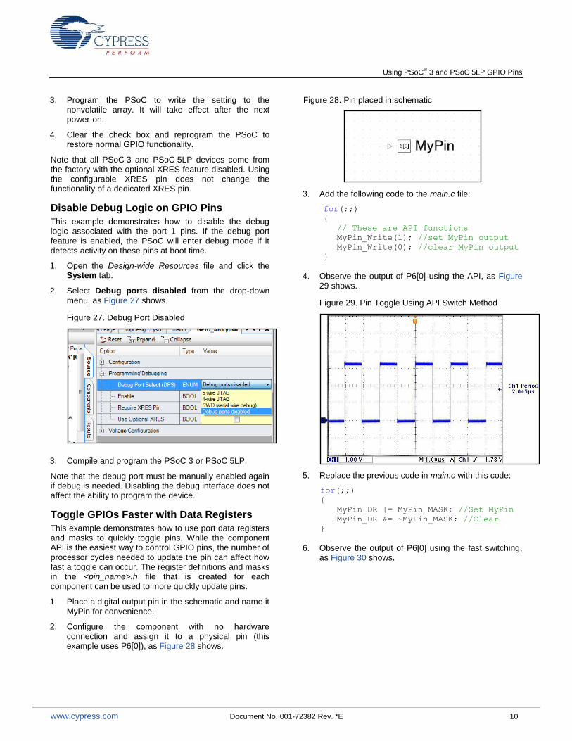
1. Place a digital output pin in the schematic and name it MyPin for convenience.
2. Configure the component with no hardware connection and assign it to a physical pin (this example uses P6[0]), as Figure 28 shows.
Figure 28. Pin placed in schematic
3. Add the following code to the main.c file:
for(;;)
{
// These are API functions
MyPin_Write(1); //set MyPin output
MyPin_Write(0); //clear MyPin output
}
4. Observe the output of P6[0] using the API, as Figure 29 shows.
Figure 29. Pin Toggle Using API Switch Method
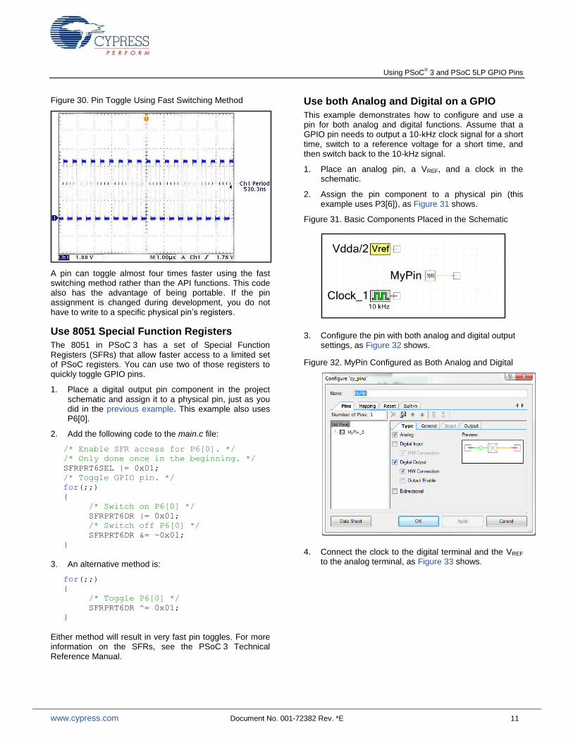
5. Replace the previous code in main.c with this code:
for(;;)
{
MyPin_DR |= MyPin_MASK; //Set MyPin
MyPin_DR &= ~MyPin_MASK; //Clear
}
6. Observe the output of P6[0] using the fast switching, as Figure 30 shows.
Using PSoC® 3 and PSoC 5LP GPIO Pins
www.cypress.com Document No. 001-72382 Rev. *E 11
Figure 30. Pin Toggle Using Fast Switching Method
A pin can toggle almost four times faster using the fast switching method rather than the API functions. This code also has the advantage of being portable. If the pin assignment is changed during development, you do not have to write to a specific physical pin‘s registers.
Use 8051 Special Function Registers
The 8051 in PSoC 3 has a set of Special Function Registers (SFRs) that allow faster access to a limited set of PSoC registers. You can use two of those registers to quickly toggle GPIO pins.
1. Place a digital output pin component in the project schematic and assign it to a physical pin, just as you did in the previous example. This example also uses P6[0].
2. Add the following code to the main.c file:
/* Enable SFR access for P6[0]. */
/* Only done once in the beginning. */
SFRPRT6SEL |= 0x01;
/* Toggle GPIO pin. */
for(;;)
{
/* Switch on P6[0] */
SFRPRT6DR |= 0x01;
/* Switch off P6[0] */
SFRPRT6DR &= ~0x01;
}
3. An alternative method is:
for(;;)
{
/* Toggle P6[0] */
SFRPRT6DR ^= 0x01;
}
Either method will result in very fast pin toggles. For more information on the SFRs, see the PSoC 3 Technical Reference Manual.
Use both Analog and Digital on a GPIO
This example demonstrates how to configure and use a pin for both analog and digital functions. Assume that a GPIO pin needs to output a 10-kHz clock signal for a short time, switch to a reference voltage for a short time, and then switch back to the 10-kHz signal.
1. Place an analog pin, a VREF, and a clock in the schematic.
2. Assign the pin component to a physical pin (this example uses P3[6]), as Figure 31 shows.
Figure 31. Basic Components Placed in the Schematic
3. Configure the pin with both analog and digital output settings, as Figure 32 shows.
Figure 32. MyPin Configured as Both Analog and Digital
4. Connect the clock to the digital terminal and the VREF to the analog terminal, as Figure 33 shows.
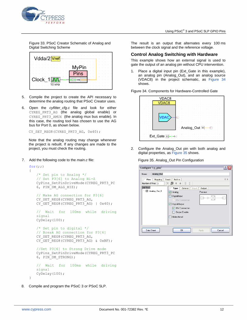
Using PSoC® 3 and PSoC 5LP GPIO Pins
www.cypress.com Document No. 001-72382 Rev. *E 12
Figure 33. PSoC Creator Schematic of Analog and Digital Switching Scheme
5. Compile the project to create the API necessary to determine the analog routing that PSoC Creator uses.
6. Open the cyfitter_cfg.c file and look for either
CYREG_PRT3_AG (the analog global enable) or
CYREG_PRT3_AMUX (the analog mux bus enable). In
this case, the routing tool has chosen to use the AG bus for Port 0, as shown below.
CY_SET_REG8(CYREG_PRT3_AG, 0x40);
Note that the analog routing may change whenever the project is rebuilt. If any changes are made to the project, you must check the routing.
7. Add the following code to the main.c file:
for(;;)
{
/* Set pin to Analog */
// Set P3[6] to Analog Hi-Z
CyPins_SetPinDriveMode(CYREG_PRT3_PC
6, PIN_DM_ALG_HIZ);
// Make AG connection for P3[6]
CY_SET_REG8(CYREG_PRT3_AG,
CY_GET_REG8(CYREG_PRT3_AG) | 0x40);
// Wait for 100ms while driving
signal
CyDelay(100);
/* Set pin to digital */
// Break AG connection for P3[6]
CY_SET_REG8(CYREG_PRT3_AG,
CY_GET_REG8(CYREG_PRT3_AG) & 0xBF);
//Set P3[6] to Strong Drive mode
CyPins_SetPinDriveMode(CYREG_PRT3_PC
6, PIN_DM_STRONG);
// Wait for 100ms while driving
signal
CyDelay(100);
}
8. Compile and program the PSoC 3 or PSoC 5LP.
The result is an output that alternates every 100 ms between the clock signal and the reference voltage.
Control Analog Switching with Hardware
This example shows how an external signal is used to gate the output of an analog pin without CPU intervention.
1. Place a digital input pin (Ext_Gate in this example), an analog pin (Analog_Out), and an analog source (VDAC8) in the project schematic, as Figure 34 shows.
Figure 34. Components for Hardware-Controlled Gate
2. Configure the Analog_Out pin with both analog and digital properties, as Figure 35 shows.
Figure 35. Analog_Out Pin Configuration
Using PSoC® 3 and PSoC 5LP GPIO Pins
www.cypress.com Document No. 001-72382 Rev. *E 13
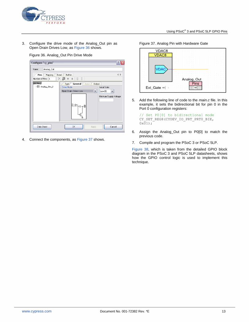
3. Configure the drive mode of the Analog_Out pin as Open Drain Drives Low, as Figure 36 shows.
Figure 36. Analog_Out Pin Drive Mode
4. Connect the components, as Figure 37 shows.
Figure 37. Analog Pin with Hardware Gate
5. Add the following line of code to the main.c file. In this example, it sets the bidirectional bit for pin 0 in the Port 0 configuration registers:
// Set P0[0] to bidirectional mode
CY_SET_REG8(CYDEV_IO_PRT_PRT0_BIE,
0x01);
6. Assign the Analog_Out pin to P0[0] to match the previous code.
7. Compile and program the PSoC 3 or PSoC 5LP.
Figure 38, which is taken from the detailed GPIO block diagram in the PSoC 3 and PSoC 5LP datasheets, shows how the GPIO control logic is used to implement this technique.
Using PSoC® 3 and PSoC 5LP GPIO Pins
www.cypress.com Document No. 001-72382 Rev. *E 14
Figure 38. Highlighted GPIO Block Diagram from the PSoC 3 and PSoC 5LP Datasheets
Drive
Logic
PRT[x]DM0
PRT[x]DR
Digital Output Path
PRT[x]SLW
PRT[x]DM1
PRT[x]DM2
Analog
Analog Mux
Analog Global
DSI Output
PRT[x]BYP
PRT[x]BIE
Bidir Control
Capsense Control
Switches
Vddio
Vddio
PRT[x]AMUX
PRT[x]AG
1
CAPS[x]CFG1
OE
In
PRT[x]SYNC_OUT
(VDAC8)
(Ext_Gate)
(Analog_Out)
0
1 0
1
0
1
The Ext_Gate signal is routed through the DSI to the digital portion of the Analog_Out pin. The signal from the DSI (red) is routed to the analog switches because the port bidirectional bit and the analog global select bit are set (yellow). The VDAC output (blue) is switched on or off depending on the logic state of the Ext_Gate signal.
For more details on the analog switching available in the PSoC 3 and PSoC 5LP devices, see the Analog Routing section of the TRM. Another good resource is application note AN58827 – PSoC 3 and PSoC 5LP Internal Analog Routing Considerations.
Use the DSI as a Clock Source
This example demonstrates how to use a digital signal routed through the DSI as a clock source. As many as eight digital and four analog clocks can be created from an arbitrary DSI signal. Also, the PSoC can use an arbitrary digital signal as an input source for the PLL.
1. Place a digital input pin, a digital output pin, and a clock in the schematic, as Figure 39 shows.
Figure 39. Basic Components for DSI Clock Example
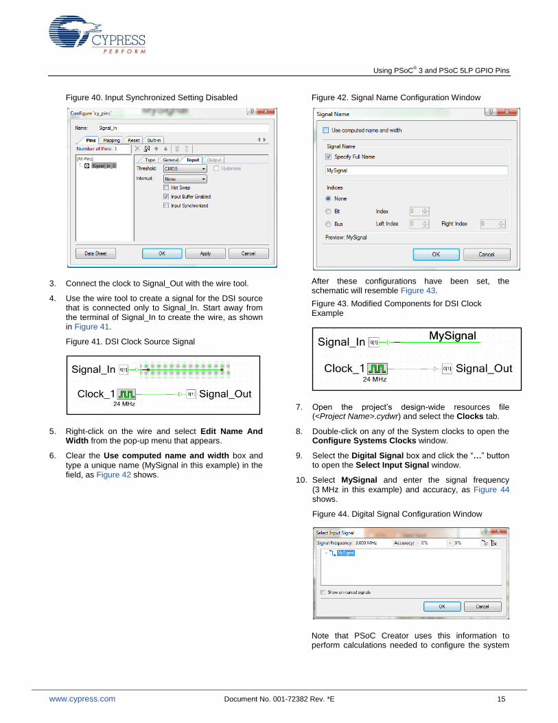
2. Open the configuration dialog for Signal_In and clear the Input Synchronized box in the pin configuration
window, as Figure 40 shows. This is necessary to prevent the signal from trying to sync to itself.
Using PSoC® 3 and PSoC 5LP GPIO Pins
www.cypress.com Document No. 001-72382 Rev. *E 15
Figure 40. Input Synchronized Setting Disabled
3. Connect the clock to Signal_Out with the wire tool.
4. Use the wire tool to create a signal for the DSI source that is connected only to Signal_In. Start away from the terminal of Signal_In to create the wire, as shown in Figure 41.
Figure 41. DSI Clock Source Signal
5. Right-click on the wire and select Edit Name And Width from the pop-up menu that appears.
6. Clear the Use computed name and width box and
type a unique name (MySignal in this example) in the field, as Figure 42 shows.
Figure 42. Signal Name Configuration Window
After these configurations have been set, the schematic will resemble Figure 43.
Figure 43. Modified Components for DSI Clock Example
7. Open the project‘s design-wide resources file (<Project Name>.cydwr) and select the Clocks tab.
8. Double-click on any of the System clocks to open the Configure Systems Clocks window.
9. Select the Digital Signal box and click the ―…‖ button to open the Select Input Signal window.
10. Select MySignal and enter the signal frequency
(3 MHz in this example) and accuracy, as Figure 44 shows.
Figure 44. Digital Signal Configuration Window
Note that PSoC Creator uses this information to perform calculations needed to configure the system
Using PSoC® 3 and PSoC 5LP GPIO Pins
www.cypress.com Document No. 001-72382 Rev. *E 16
clocks. Make sure that the signal information is accurate.
11. Set the input source for the IMO and PLL to ―Digital Signal‖, as Figure 45 shows.
Figure 45. DSI Signal as the Source for the IMO and PLL
The PLL uses the 3-MHz input to generate a 24-MHz output, which is routed to the Master and Bus clocks to generate the Signal_Out clock.
For more details on the DSI system clocking, see the Datasheet, TRM, and Cypress application note AN60631 – PSoC
® 3 Clocking Resources.
Change PICU Settings with Firmware
Dynamic configuration of the PICU is done through a write
to bits [1:0] of the PICUx_INTTYPEy register, where the
‗x‘ corresponds to the port number and ‗y‘ corresponds to the pin number (see Table 2). You can change the configuration at any time to enable or disable pin interrupts.
Table 2. PICU Interrupt Types and Bit Settings
Bits 1:0 Name Description
00 Disable Interrupts disabled
01 Rising Edge Trigger on rising edge
10 Falling Edge Trigger on falling edge
11 Change Mode Trigger on any edge
In this example, pin P6[0] is configured as a rising-edge interrupt, and P6[1] is configured as a falling-edge interrupt.
1. Place two digital input pins in the project schematic.
2. Assign the pins to P6[0] and P6[1].
3. Configure P6[0] as a resistive pull-down pin, or add an external pull-down.
4. Configure P6[1] as a resistive pull-up pin, or add an external pull-up.
5. Add the following code to the main.c file:
//Set P6[0] to PICU rising-edge trigger
CY_SET_REG8(CYREG_PICU6_INTTYPE0,
0x01);
//Set P6[1] to PICU falling-edge
trigger
CY_SET_REG8(CYREG_PICU6_INTTYPE1,
0x02);
//Sleep and wait for PICU interrupt
//Sleep again if not P6[1] PICU wakeup
do
{
//Save clocks and enter sleep
CyPmSaveClocks();
CyPmSleep(PM_SLEEP_TIME_NONE,
PM_SLEEP_SRC_PICU);
CyPmRestoreClocks();
//Stay awake for two seconds
CyDelay(2000);
}
while
(!(CY_GET_REG8(CYREG_PICU6_INTSTAT) &
0x02));
//Disable P6[1] PICU trigger
CY_SET_REG8(CYREG_PICU6_INTTYPE1,
0x00);
6. Compile and program.
The PSoC will wake from sleep on any PICU interrupt, but it will return to sleep again unless P6[1] was the trigger. You are not required to disable the interrupts after wakeup. They can be used during normal operation like any other interrupt source.
The PSoC 3 or PSoC 5LP TRM has further information about the PICU, including block diagrams and functional descriptions. Another good resource is application note AN54460, PSoC 3 and PSoC 5LP Interrupts.
Using PSoC® 3 and PSoC 5LP GPIO Pins
www.cypress.com Document No. 001-72382 Rev. *E 17
Gang Pins for More Drive/Sink Current
To increase the total source/sink capabilities of the circuit GPIO pins can be ganged (shorted together). The limitations of VDDIO quadrants still apply. This example demonstrates driving a PWM signal with four GPIO pins.
1. Place and configure a PWM and a Clock component.
2. Place a single digital output pin component and connect it to the PWM output terminal, as Figure 46 shows.
Figure 46. Single Pin Placed in Schematic
3. Open the Pins configuration dialog and set the number of pins accordingly, as Figure 47 shows. This example uses four GPIO pins.
Figure 47. Configure Multiple Pins in the Component
4. Optionally, set the pin mapping to Contiguous for
easier PCB routing, as Figure 48 shows.
Figure 48. Enable Contiguous Mapping
5. Assign the Pin component to physical pins.
6. Connect the signal source (PWM in this example) to each of the pin terminals in the component, as shown in Figure 49.
Figure 49. Ganged Pins Symbol
7. Compile and program the PSoC 3 or PSoC 5LP.
The output of the PWM will be driven on all four GPIOs. The pins can be shorted externally on the PCB and connected to the external circuit as needed.
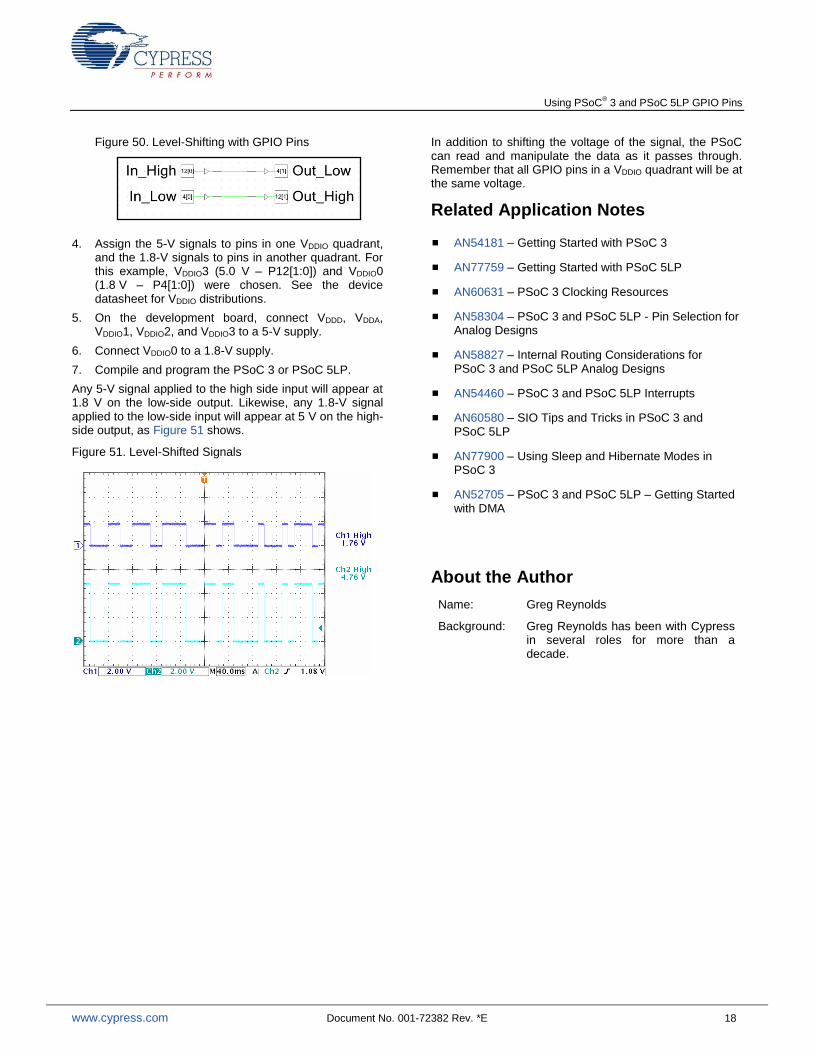
Level-Shift Signals
The GPIO pins can be used for level-shifting of signals by powering the VDDIO pins at different voltages. The only limitation is that no VDDIO quadrant may be at a higher voltage than VDDA. This example demonstrates how to create a simple 5-V/1.8-V level shifting configuration in the PSoC 3 or PSoC 5LP.
1. Place two High-Z digital input pins and two Strong Drive digital output pins in the project schematic.
2. Connect one of the inputs to one of the outputs. Connect the remaining input to the remaining output.
3. For convenience, give the pin symbols meaningful names similar to the ones shown in Figure 50.
Using PSoC® 3 and PSoC 5LP GPIO Pins
www.cypress.com Document No. 001-72382 Rev. *E 18
Figure 50. Level-Shifting with GPIO Pins
4. Assign the 5-V signals to pins in one VDDIO quadrant, and the 1.8-V signals to pins in another quadrant. For this example, VDDIO3 (5.0 V – P12[1:0]) and VDDIO0 (1.8 V – P4[1:0]) were chosen. See the device datasheet for VDDIO distributions.
5. On the development board, connect VDDD, VDDA, VDDIO1, VDDIO2, and VDDIO3 to a 5-V supply.
6. Connect VDDIO0 to a 1.8-V supply.
7. Compile and program the PSoC 3 or PSoC 5LP.
Any 5-V signal applied to the high side input will appear at 1.8 V on the low-side output. Likewise, any 1.8-V signal applied to the low-side input will appear at 5 V on the high-side output, as Figure 51 shows.
Figure 51. Level-Shifted Signals
In addition to shifting the voltage of the signal, the PSoC can read and manipulate the data as it passes through. Remember that all GPIO pins in a VDDIO quadrant will be at the same voltage.
Related Application Notes
AN54181 – Getting Started with PSoC 3
AN77759 – Getting Started with PSoC 5LP
AN60631 – PSoC 3 Clocking Resources
AN58304 – PSoC 3 and PSoC 5LP - Pin Selection for Analog Designs
AN58827 – Internal Routing Considerations for PSoC 3 and PSoC 5LP Analog Designs
AN54460 – PSoC 3 and PSoC 5LP Interrupts
AN60580 – SIO Tips and Tricks in PSoC 3 and PSoC 5LP
AN77900 – Using Sleep and Hibernate Modes in PSoC 3
AN52705 – PSoC 3 and PSoC 5LP – Getting Started with DMA
About the Author
Name: Greg Reynolds
Background: Greg Reynolds has been with Cypress in several roles for more than a decade.
Using PSoC® 3 and PSoC 5LP GPIO Pins
www.cypress.com Document No. 001-72382 Rev. *E 19
Appendix A: GPIO API and Register Reference
Component API
The Pins component API is used to access all physical pins associated with a component. The instance name of the component, either assigned by the user or generated by PSoC Creator, is used as the prefix for the function name. The component APIs are documented in detail in the Pins Component datasheet. Table 3 lists the component functions.
Table 3. Component API Reference
API Description Example (using a component name of MyPin)
<Pin_Name>_Read Returns the current value for all pins in the component.
myVar = MyPin_Read();
<Pin_Name>_Write Writes the value to the component pins. MyPin_Write(1);
<Pin_Name>_ReadDataReg Returns the current value for all pins in the component.
myVar = MyPin_ReadDataReg();
<Pin_Name>_SetDriveMode Sets the drive mode for each of the component‘s pins.
MyPin_SetDriveMode(MyPin_DM_ALG_HIZ);
<Pin_Name>_ClearInterrupt Clears any active interrupts on the port into which the component is mapped. Returns the value of interrupt status register.
myVar = MyPin_ClearInterrupt();
Per-Pin API
You can access individual physical pins by using the global per-pin API macros. The physical pins do not need to be associated with a Pins component because the macros directly access the pin configuration registers. Using per-pin APIs can result in undefined behavior in any physical pin associated with a Pins component due to conflicts with the component configuration. The per-pin APIs are documented in detail in the PSoC Creator System Reference Guide. Table 4 lists the per-pin functions.
Table 4. Per-Pin API Reference
API Description Example (using P1[2])
CyPins_ReadPin Reads the current value on the pin.
myVar = CyPins_ReadPin(CYREG_PRT1_PC2);
CyPins_SetPin Sets the output value for the pin to logic high.
CyPins_SetPin(CYREG_PRT1_PC2);
CyPins_ClearPin Sets the output value for the pin to a logic low.
CyPins_ClearPin(CYREG_PRT1_PC2);
CyPins_SetPinDriveMode Sets the drive mode for the pin.
CyPins_SetPinDriveMode(CYREG_PRT1_PC2,
PIN_DM_ALG_HIZ);
CyPins_ReadPinDriveMode Reads the drive mode for the pin.
myVar = CyPins_ReadPinDriveMode(CYREG_PRT1_PC2);
CyPins_FastSlew() Sets the slew rate for the pin to fast edge rate.
CyPins_FastSlew(CYREG_PRT1_PC2);
CyPins_SlowSlew() Sets the slew rate for the pin to slow edge rate.
CyPins_SlowSlew(CYREG_PRT1_PC2);
Using PSoC® 3 and PSoC 5LP GPIO Pins
www.cypress.com Document No. 001-72382 Rev. *E 20
GPIO Registers
The following registers are used to configure the GPIOs. They are accessible by firmware during normal operation. Further details and register maps are in the PSoC 3 and PSoC 5LP Register TRM documents that are available for free from the Cypress website. Table 5 lists the GPIO registers.
Table 5. GPIO Registers
Register Name Description
PRTx_PCy[7:0] Port Pin Configuration This register accesses several configuration or status bits of a single I/O port pin at once.
PRTx_DR[7:0] Port Data Output This register is used to set the output data state for the corresponding GPIO port.
PRTx_PS[7:0] Port Pin State This register holds the logical pin state for the corresponding GPIO port. If the drive mode for the pin is set to High-Z Analog, the state will always read 0.
PRTx_DM2[7:0]
PRTx_DM1[7:0]
PRTx_DM0[7:0]
Port Drive Mode These registers‘ combined value determines the unique drive mode of each bit in a GPIO port.
PRTx_SLW[7:0] Port Slew Rate Control This register is used to set a fast or slow edge rate for any strong drive mode GPIO pin.
PRTx_BYP[7:0] Port Bypass Enable This register selects whether the output data for the corresponding GPIO is sourced from the DSI or port logic data register.
PRTx_BIE[7:0] Port Bidirection Enable This register is used to enable dynamic bidirectional control through the DSI.
PRTx_INP_DIS[7:0] Input Buffer Disable Override This register is used to force the input buffers off.
PRTx_CTL[0] Port Wide Control Signals This register is used to select the internal buffer trip point.
PRTx_PRT[7:5,3:1] Port Wide Configuration This register accesses several available configuration registers on a port-wide basis with a single bit write.
PRTx_BIT_MASK[7:0] Bitmask for Aliased Register Access This register allows or blocks access to the data registers from the aliased register address space.
PRTx_AMUX[7:0] Port Analog Global mux Bus Enable This register controls the analog global mux switch for the corresponding GPIO port.
PRTx_AG[7:0] Port Analog Global Enable This register controls the analog global switch for the corresponding GPIO port.
PICUx_INTTYPE[1:0] Port Interrupt Control Type This register configures the type of interrupt for the corresponding GPIO pin.
PICUx_INTSTAT[7:0] Port Interrupt Control Status This register shows posted interrupts for the corresponding GPIO port.
PICUx_SNAP[7:0] Port Interrupt Control Snap Shot This register shows the state of input pins at the last read of the PICUx_INTSTAT register.
PICUx_DISABLE_COR[0] Disable Status Register Clear on Read Feature
This register disables the ―clear on read‖ feature of the PICUx_INTSTAT register.
Using PSoC® 3 and PSoC 5LP GPIO Pins
www.cypress.com Document No. 001-72382 Rev. *E 21
Nonvolatile Latches
The PSoC 3 and PSoC 5LP have an array of nonvolatile latches (NVLs) that are used to configure the device behavior in reset. The following latches are used to configure the GPIOs. They are not accessible from firmware during normal operation. Further details and register maps for the NVL array are in the Nonvolatile Latches section of the PSoC 3 and PSoC 5LP
datasheets and TRM. Table 6 lists the NVL latches.
Table 6. NVL Latches Relating to GPIOs
NVL Latch Name Description
PRTxRDM[1:0] Port Reset Drive mode Controls reset drive mode of the corresponding I/O port.
XRESMEN[0] Optional XRES Enable Controls whether pin P1[2] is used as a GPIO or as an external reset.
DPS[1:0] Debug Port Select Controls the usage of various Port1 pins as a debug port.
Using PSoC® 3 and PSoC 5LP GPIO Pins
www.cypress.com Document No. 001-72382 Rev. *E 22
Appendix B: PSoC Creator Settings and Registers
The GPIO settings established in PSoC Creator are part of the cy_boot startup code and take effect during initial device configuration. The tables in this appendix show the relationship between the settings in the Pins Component configuration window and the GPIO registers. In addition, simple code examples demonstrate how to perform the same function in firmware during normal operation, if applicable. The configuration window may look slightly different, depending on which version of Creator you are using.
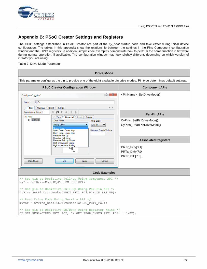
Table 7. Drive Mode Parameter
Drive Mode
This parameter configures the pin to provide one of the eight available pin drive modes. Pin type determines default settings.
PSoC Creator Configuration Window Component APIs
<PinName>_SetDriveMode()
Per-Pin APIs
CyPins_SetPinDriveMode()
CyPins_ReadPinDriveMode()
Associated Registers
PRTx_PCy[3:1]
PRTx_DMy[7:0]
PRTx_BIE[7:0]
Code Examples
/* Set pin to Resistive Pull-up Using Component API */
MyPin_SetDriveMode(MyPin_DM_RES_UP);
/* Set pin to Resistive Pull-up Using Per-Pin API */
CyPins_SetPinDriveMode(CYREG_PRT1_PC2,PIN_DM_RES_UP);
/* Read Drive Mode Using Per-Pin API */
myVar = CyPins_ReadPinDriveMode(CYREG_PRT1_PC2);
/* Set pin to Resistive Up/Down Using Register Write */
CY_SET_REG8(CYREG_PRT1_PC2, CY_GET_REG8(CYREG_PRT1_PC2) | 0x07);
Using PSoC® 3 and PSoC 5LP GPIO Pins
www.cypress.com Document No. 001-72382 Rev. *E 23
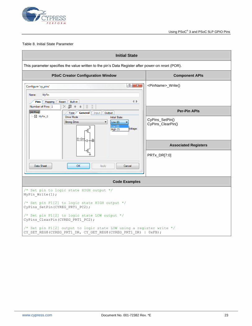
Table 8. Initial State Parameter
Initial State
This parameter specifies the value written to the pin‘s Data Register after power-on reset (POR).
PSoC Creator Configuration Window Component APIs
<PinName>_Write()
Per-Pin APIs
CyPins_SetPin() CyPins_ClearPin()
Associated Registers
PRTx_DR[7:0]
Code Examples
/* Set pin to logic state HIGH output */
MyPin_Write(1);
/* Set pin P1[2] to logic state HIGH output */
CyPins_SetPin(CYREG_PRT1_PC2);
/* Set pin P1[2] to logic state LOW output */
CyPins_ClearPin(CYREG_PRT1_PC2);
/* Set pin P1[2] output to logic state LOW using a register write */
CY_SET_REG8(CYREG_PRT1_DR, CY_GET_REG8(CYREG_PRT1_DR) | 0xFB);
Using PSoC® 3 and PSoC 5LP GPIO Pins
www.cypress.com Document No. 001-72382 Rev. *E 24
Table 9. Threshold Parameter
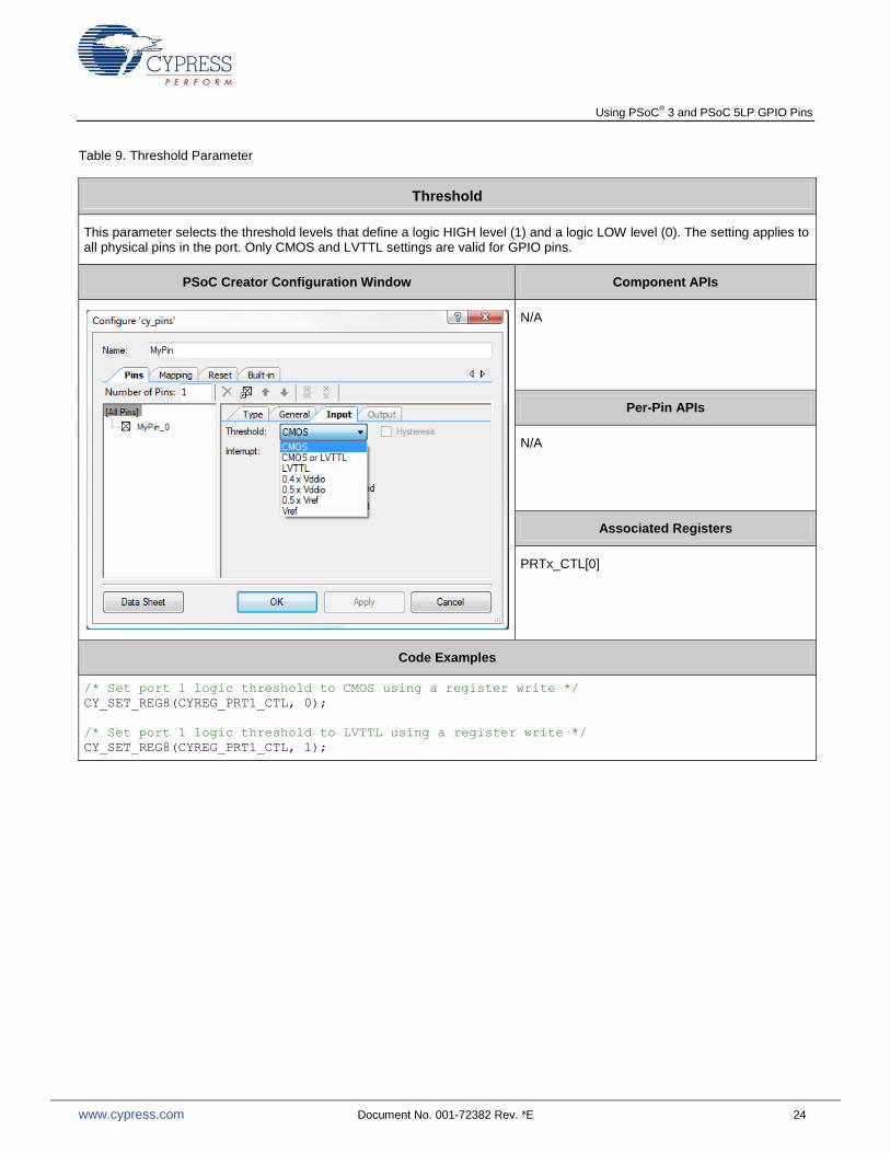
Threshold
This parameter selects the threshold levels that define a logic HIGH level (1) and a logic LOW level (0). The setting applies to all physical pins in the port. Only CMOS and LVTTL settings are valid for GPIO pins.
PSoC Creator Configuration Window Component APIs
N/A
Per-Pin APIs
N/A
Associated Registers
PRTx_CTL[0]
Code Examples
/* Set port 1 logic threshold to CMOS using a register write */
CY_SET_REG8(CYREG_PRT1_CTL, 0);
/* Set port 1 logic threshold to LVTTL using a register write */
CY_SET_REG8(CYREG_PRT1_CTL, 1);
Using PSoC® 3 and PSoC 5LP GPIO Pins
www.cypress.com Document No. 001-72382 Rev. *E 25
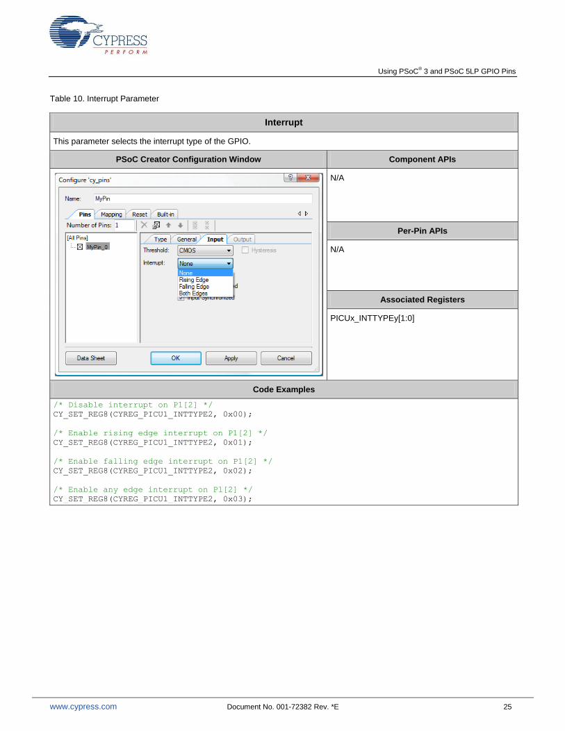
Table 10. Interrupt Parameter
Interrupt
This parameter selects the interrupt type of the GPIO.
PSoC Creator Configuration Window Component APIs
N/A
Per-Pin APIs
N/A
Associated Registers
PICUx_INTTYPEy[1:0]
Code Examples
/* Disable interrupt on P1[2] */
CY_SET_REG8(CYREG_PICU1_INTTYPE2, 0x00);
/* Enable rising edge interrupt on P1[2] */
CY_SET_REG8(CYREG_PICU1_INTTYPE2, 0x01);
/* Enable falling edge interrupt on P1[2] */
CY_SET_REG8(CYREG_PICU1_INTTYPE2, 0x02);
/* Enable any edge interrupt on P1[2] */
CY_SET_REG8(CYREG_PICU1_INTTYPE2, 0x03);
Using PSoC® 3 and PSoC 5LP GPIO Pins
www.cypress.com Document No. 001-72382 Rev. *E 26
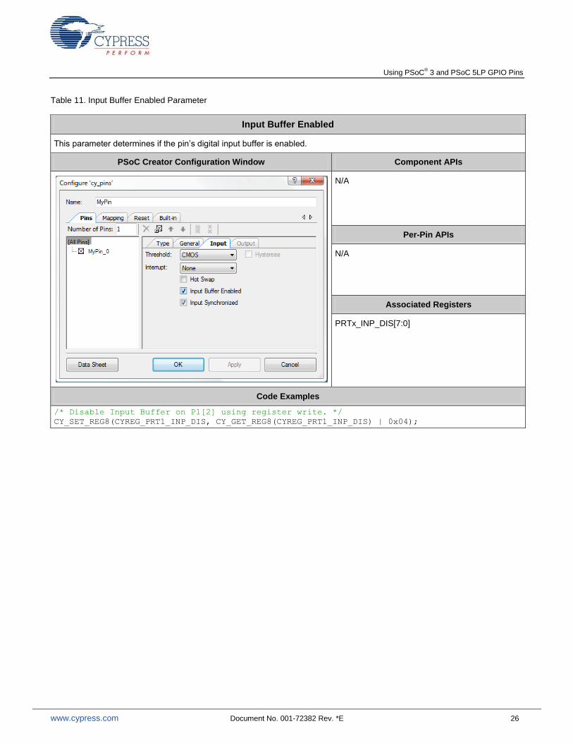
Table 11. Input Buffer Enabled Parameter
Input Buffer Enabled
This parameter determines if the pin‘s digital input buffer is enabled.
PSoC Creator Configuration Window Component APIs
N/A
Per-Pin APIs
N/A
Associated Registers
PRTx_INP_DIS[7:0]
Code Examples
/* Disable Input Buffer on P1[2] using register write. */
CY_SET_REG8(CYREG_PRT1_INP_DIS, CY_GET_REG8(CYREG_PRT1_INP_DIS) | 0x04);
Using PSoC® 3 and PSoC 5LP GPIO Pins
www.cypress.com Document No. 001-72382 Rev. *E 27
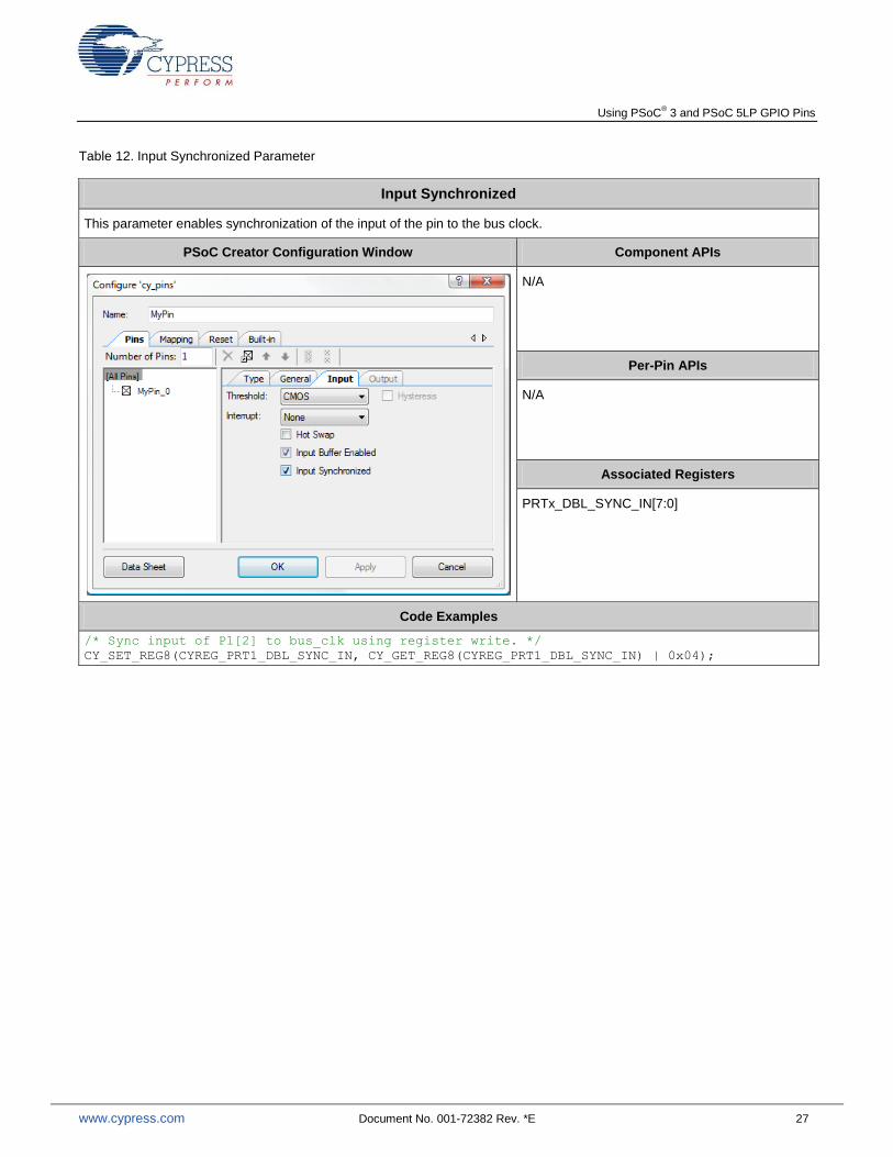
Table 12. Input Synchronized Parameter
Input Synchronized
This parameter enables synchronization of the input of the pin to the bus clock.
PSoC Creator Configuration Window Component APIs
N/A
Per-Pin APIs
N/A
Associated Registers
PRTx_DBL_SYNC_IN[7:0]
Code Examples
/* Sync input of P1[2] to bus_clk using register write. */
CY_SET_REG8(CYREG_PRT1_DBL_SYNC_IN, CY_GET_REG8(CYREG_PRT1_DBL_SYNC_IN) | 0x04);
Using PSoC® 3 and PSoC 5LP GPIO Pins
www.cypress.com Document No. 001-72382 Rev. *E 28
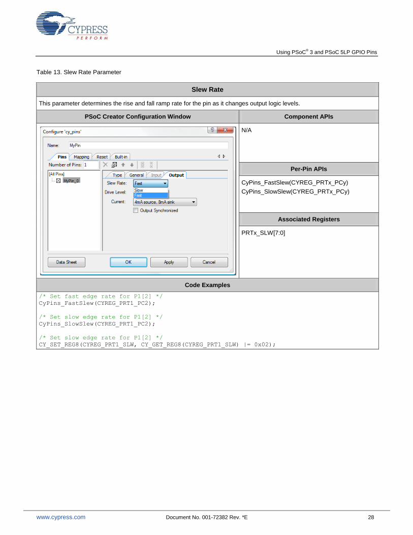
Table 13. Slew Rate Parameter
Slew Rate
This parameter determines the rise and fall ramp rate for the pin as it changes output logic levels.
PSoC Creator Configuration Window Component APIs
N/A
Per-Pin APIs
CyPins_FastSlew(CYREG_PRTx_PCy)
CyPins_SlowSlew(CYREG_PRTx_PCy)
Associated Registers
PRTx_SLW[7:0]
Code Examples
/* Set fast edge rate for P1[2] */
CyPins_FastSlew(CYREG_PRT1_PC2);
/* Set slow edge rate for P1[2] */
CyPins_SlowSlew(CYREG_PRT1_PC2);
/* Set slow edge rate for P1[2] */
CY_SET_REG8(CYREG_PRT1_SLW, CY_GET_REG8(CYREG_PRT1_SLW) |= 0x02);

Using PSoC® 3 and PSoC 5LP GPIO Pins
www.cypress.com Document No. 001-72382 Rev. *E 29
Table 14. Output Synchronized Parameter
Output Synchronized
This parameter synchronizes the output drivers of the pin to the bus_clk.
PSoC Creator Configuration Window Component APIs
N/A
Per-Pin APIs
N/A
Associated Registers
PRTx_SYNC_OUT[7:0]
Code Examples
/* Sync output of P1[2] to bus clock using register write. */
CY_SET_REG8(CYREG_PRT1_SYNC_OUT, CY_GET_REG8(CYREG_PRT1_SYNC_OUT) | 0x04);
Using PSoC® 3 and PSoC 5LP GPIO Pins
www.cypress.com Document No. 001-72382 Rev. *E 30
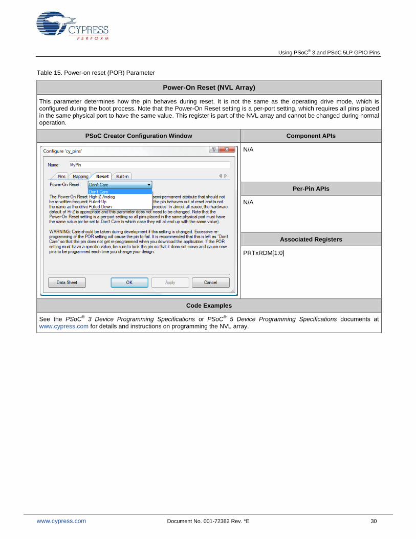
Table 15. Power-on reset (POR) Parameter
Power-On Reset (NVL Array)
This parameter determines how the pin behaves during reset. It is not the same as the operating drive mode, which is configured during the boot process. Note that the Power-On Reset setting is a per-port setting, which requires all pins placed in the same physical port to have the same value. This register is part of the NVL array and cannot be changed during normal operation.
PSoC Creator Configuration Window Component APIs
N/A
Per-Pin APIs
N/A
Associated Registers
PRTxRDM[1:0]
Code Examples
See the PSoC® 3 Device Programming Specifications or PSoC
® 5 Device Programming Specifications documents at
www.cypress.com for details and instructions on programming the NVL array.
Using PSoC® 3 and PSoC 5LP GPIO Pins
www.cypress.com Document No. 001-72382 Rev. *E 31
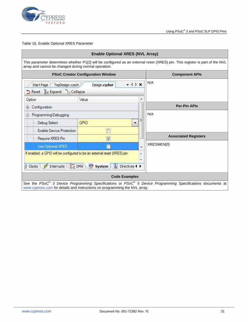
Table 16. Enable Optional XRES Parameter
Enable Optional XRES (NVL Array)
This parameter determines whether P1[2] will be configured as an external reset (XRES) pin. This register is part of the NVL array and cannot be changed during normal operation.
PSoC Creator Configuration Window Component APIs
N/A
Per-Pin APIs
N/A
Associated Registers
XRESMEN[0]
Code Examples
See the PSoC® 3 Device Programming Specifications or PSoC
® 5 Device Programming Specifications documents at
www.cypress.com for details and instructions on programming the NVL array.
Using PSoC® 3 and PSoC 5LP GPIO Pins
www.cypress.com Document No. 001-72382 Rev. *E 32
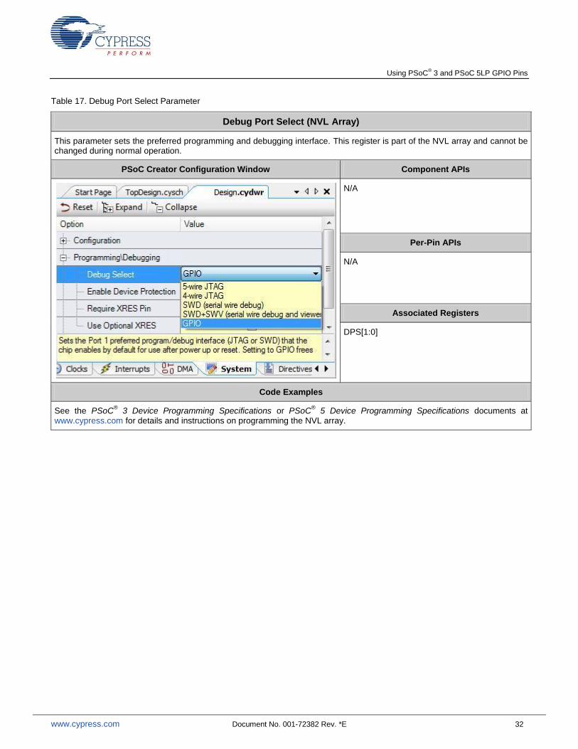
Table 17. Debug Port Select Parameter
Debug Port Select (NVL Array)
This parameter sets the preferred programming and debugging interface. This register is part of the NVL array and cannot be changed during normal operation.
PSoC Creator Configuration Window Component APIs
N/A
Per-Pin APIs
N/A
Associated Registers
DPS[1:0]
Code Examples
See the PSoC® 3 Device Programming Specifications or PSoC
® 5 Device Programming Specifications documents at
www.cypress.com for details and instructions on programming the NVL array.
Using PSoC® 3 and PSoC 5LP GPIO Pins
www.cypress.com Document No. 001-72382 Rev. *E 33
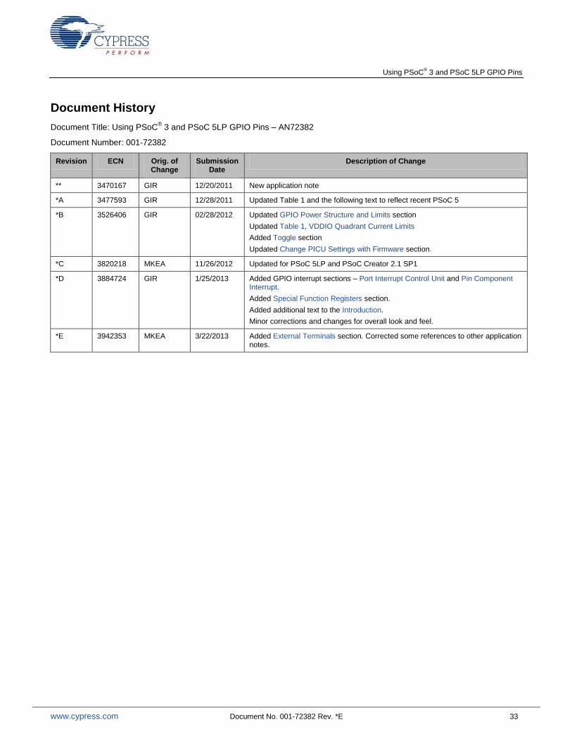
Document History
Document Title: Using PSoC® 3 and PSoC 5LP GPIO Pins – AN72382
Document Number: 001-72382
Revision ECN Orig. of Change
Submission Date
Description of Change
** 3470167 GIR 12/20/2011 New application note
*A 3477593 GIR 12/28/2011 Updated Table 1 and the following text to reflect recent PSoC 5
*B 3526406 GIR 02/28/2012 Updated GPIO Power Structure and Limits section
Updated Table 1, VDDIO Quadrant Current Limits
Added Toggle section
Updated Change PICU Settings with Firmware section.
*C 3820218 MKEA 11/26/2012 Updated for PSoC 5LP and PSoC Creator 2.1 SP1
*D 3884724 GIR 1/25/2013 Added GPIO interrupt sections – Port Interrupt Control Unit and Pin Component Interrupt.
Added Special Function Registers section.
Added additional text to the Introduction.
Minor corrections and changes for overall look and feel.
*E 3942353 MKEA 3/22/2013 Added External Terminals section. Corrected some references to other application notes.
Using PSoC® 3 and PSoC 5LP GPIO Pins
www.cypress.com Document No. 001-72382 Rev. *E 34
Products
Automotive cypress.com/go/automotive
Clocks & Buffers cypress.com/go/clocks
Interface cypress.com/go/interface
Lighting & Power Control cypress.com/go/powerpsoc cypress.com/go/plc
Memory cypress.com/go/memory
PSoC cypress.com/go/psoc
Touch Sensing cypress.com/go/touch
USB Controllers cypress.com/go/usb
Wireless/RF cypress.com/go/wireless
PSoC® Solutions
psoc.cypress.com/solutions
PSoC 1 | PSoC 3 | PSoC 5LP
Cypress Developer Community
Community | Forums | Blogs | Video | Training
Technical Support
cypress.com/go/support
PSoC is a registered trademark of Cypress Semiconductor Corp. ―Programmable System-on-Chip‖ and PSoC Creator are trademarks of Cypress Semiconductor Corp. All other trademarks or registered trademarks referenced herein are the property of their respective owners.
Cypress Semiconductor 198 Champion Court San Jose, CA 95134-1709
Phone : 408-943-2600 Fax : 408-943-4730 Website : www.cypress.com
© Cypress Semiconductor Corporation, 2013. The information contained herein is subject to change without notice. Cypress Semiconductor Corporation assumes no responsibility for the use of any circuitry other than circuitry embodied in a Cypress product. Nor does it convey or imply any license under patent or other rights. Cypress products are not warranted nor intended to be used for medical, life support, life saving, critical control or safety applications, unless pursuant to an express written agreement with Cypress. Furthermore, Cypress does not authorize its products for use as critical components in life-support systems where a malfunction or failure may reasonably be expected to result in significant injury to the user. The inclusion of Cypress products in life-support systems application implies that the manufacturer assumes all risk of such use and in doing so indemnifies Cypress against all charges. This Source Code (software and/or firmware) is owned by Cypress Semiconductor Corporation (Cypress) and is protected by and subject to worldwide patent protection (United States and foreign), United States copyright laws and international treaty provisions. Cypress hereby grants to licensee a personal, non-exclusive, non-transferable license to copy, use, modify, create derivative works of, and compile the Cypress Source Code and derivative works for the sole purpose of creating custom software and or firmware in support of licensee product to be used only in conjunction with a Cypress integrated circuit as specified in the applicable agreement. Any reproduction, modification, translation, compilation, or representation of this Source Code except as specified above is prohibited without the express written permission of Cypress. Disclaimer: CYPRESS MAKES NO WARRANTY OF ANY KIND, EXPRESS OR IMPLIED, WITH REGARD TO THIS MATERIAL, INCLUDING, BUT NOT LIMITED TO, THE IMPLIED WARRANTIES OF MERCHANTABILITY AND FITNESS FOR A PARTICULAR PURPOSE. Cypress reserves the right to make changes without further notice to the materials described herein. Cypress does not assume any liability arising out of the application or use of any product or circuit described herein. Cypress does not authorize its products for use as critical components in life-support systems where a malfunction or failure may reasonably be expected to result in significant injury to the user. The inclusion of Cypress‘ product in a life-support systems application implies that the manufacturer assumes all risk of such use and in doing so indemnifies Cypress against all charges. Use may be limited by and subject to the applicable Cypress software license agreement.
Worldwide Sales and Design Support
Cypress maintains a worldwide network of offices, solution centers, manufacturer‘s representatives, and distributors. To find the office closest to you, visit us at Cypress Locations.