Embed Size (px)
Citation preview
OP98
PRO
GRES
S R
EPO
RT
www.MaterialsViews.comwww.advopticalmat.de
Claire M. Watts , Xianliang Liu , and Willie J. Padilla *
Metamaterial Electromagnetic Wave Absorbers
The advent of negative index materials has spawned extensive research into metamaterials over the past decade. Metamaterials are attractive not only for their exotic electromagnetic properties, but also their promise for applications. A particular branch–the metamaterial perfect absorber (MPA)–has garnered interest due to the fact that it can achieve unity absorptivity of electromagnetic waves. Since its fi rst experimental demonstration in 2008, the MPA has progressed signifi cantly with designs shown across the electro-magnetic spectrum, from microwave to optical. In this Progress Report we give an overview of the fi eld and discuss a selection of examples and related applications. The ability of the MPA to exhibit extreme performance fl exibility will be discussed and the theory underlying their operation and limitations will be established. Insight is given into what we can expect from this rapidly expanding fi eld and future challenges will be addressed.
1. Introduction
The following progress report describes the history, theory, implementation, and characterization of metamaterial perfect absorbers (MPAs). It details the current state of the fi eld as well as provides a critique of the work in progress and appli-cations that have arisen or may arise from these studies. The motivation for studying MPAs comes mainly from their use in potential applications. These applications will be discussed more thoroughly in Section 6 but briefl y include: emitters, sen-sors, spatial light modulators, IR camoufl age, use in thermo-photovoltaics, and wireless communication. MPAs also provide insight into the theory of metamaterials (MMs) as an effective medium where the designer can control the electromagnetic properties by engineering the geometry.
1.1. Electromagnetic Wave Absorbers
A near unity absorber is a device in which all incident radiation is absorbed at the operating frequency–transmissivity, refl ec-tivity, scattering and all other light propagation channels are dis-abled. Electromagnetic (EM) wave absorbers can be categorized into two types: resonant absorbers and broadband absorbers. [ 1 ]
© 2012 WILEY-VCH Verlag GmbH & Co. KGaA, Weinhewileyonlinelibrary.com
C. M. Watts , X. Liu , Prof. W. J. Padilla Department of Physics Boston College Chestnut Hill, MA, 02467, USA E-mail: [email protected]
DOI: 10.1002/adma.201200674
Resonant absorbers rely on the material interacting with the incident radiation in a resonant way at a specifi c frequency, ω 0 (where the wavelength corresponding to ω 0 is λ 0 = 2 π c/ ω 0 and c is the speed of light in vacuum). Broadband absorbers gener-ally rely on materials whose properties are frequency independent and therefore can absorb radiation over a large bandwidth.
1.1.1. Resonant Absorbers
Throughout history, resonant absorbers have utilized, for the most part, multiple layers separated by a quarter of the opera-tion wavelength. In transmission line theory, a metal plate acts like a short circuit, and when it is placed λ 0 /4 behind any sort of “load,” will act like an open circuit at the
resistive sheet (i.e. conductance G = 0). [ 2 ] Therefore, the incident wave sees just the admittance of the resistive sheet. [ 2 ] When the load impedance matches free space, the refl ectivity goes to zero; this will be discussed with more detail in Section 2. [ 2 ] With the addition of loss, high absorption can be achieved.
Initial interests in electromagnetic wave absorbers were largely in the microwave range. The usefulness of absorbers in both improving radar performance and providing conceal-ment against others’ radar systems was utilized as a military technique. [ 3 ] Two well known scientists who developed EM absorbers are W. W. Salisbury and J. Jaumann, who independ-ently created similar devices. [ 4 , 5 ] One such device, known as the Salisbury screen, is a basic example of the resonant absorber mentioned above. A resistive sheet is placed λ 0 /4 in front of a metal ground plane, usually separated by some lossless dielec-tric. [ 1 , 2 ] The effective open circuit creates R ( ω 0 ) = 0 off the resis-tive layer. [ 2 ] The Jaumann absorber can conceptually be con-sidered an extension of the Salisbury screen which consists of two or more resistive sheets in front of a single ground plane. All sheets are designed to operate at a distinct wavelength, and thus each sheet is separated by approximately λ /4, producing multiple refl ection minimums around some center frequency λ 0 . The effect is that it acts as a resonant absorber over mul-tiple wavelengths, achieving a broadband response. [ 1 , 2 , 6 ] The bandwidth should increase with each added layer, however, this has the undesirable effect of making the absorber thick and bulky. [ 2 ]
The Dällenbach layer employs a different mechanism than the Salisbury screen; its design consists of a homogeneous layer in front of a ground plane. [ 1 ] The homogeneous layer is selected for particular loss values resulting from the imaginary por-tions of the electric permittivity and the magnetic permeability. The idea is to impedance match to free space as to minimize
im Adv. Mater. 2012, 24, OP98–OP120

PRO
GRES
S R
EPO
RT
www.MaterialsViews.comwww.advopticalmat.de
Claire M. Watts: Claire Watts studied physics and applied mathematics at Colgate University and received her BAS in 2010. She is cur-rently a PhD candidate in physics at Boston College and works under Professor Willie Padilla. Her research interests are in the fi eld of metamaterials and include the study of metamaterial perfect absorbers as an effec-
tive medium as well as utilizing metamaterials for imaging purposes.
Xianliang Liu: Xianliang Liu received his BS from Tianjin University, China in 2007. He is now a PhD candidate at Boston College under the supervision of Prof. Willie Padilla. His research focuses on infrared metama-terials with current research interests in realizing high
speed, large amplitude tunable infrared devices utilizing metamaterials.
Willie J. Padilla: Willie Padilla received a PhD in physics from the University of California San Diego in 2004. From 2004 to 2006, he was a Directors Postdoctoral Fellow at Los Alamos National Laboratory. In 2006 he joined the Department of Physics at Boston College and is cur-rently an Associate Professor.
In 2007 he was awarded a Young Investigator Award from the Offi ce of Naval Research and Presidential Early Career Award for Scientists and Engineers in 2011. His scientifi c interests include artifi cially structured systems including electric and magnetic metamaterials, active/dynamic meta-materials, photonics, nano-structured materials, transfor-mation optics and negative index materials.
refl ection off the surface and then utilize the loss in the homo-geneous layer to absorb the incident radiation. [ 2 ]
Another type of resonant electromagnetic wave absorber, known as the crossed grating absorber, uses a refl ective metal plane with an etched shallow periodic grid. [ 7 ] A resonance is cre-ated due to the interaction between the periodic grid and inci-dent radiation, creating a period of anomalous diffraction. This absorber had developments as early as 1902 when R. W. Wood postulated the possible effects of anomalous diffraction. [ 8 ] It was shown that anomalous diffraction is correlated to periods of enhanced absorption. [ 9 ] The total absorption of polarized light with the use of these gratings was postulated in 1976 [ 10 ] and was experimentally demonstrated soon after. [ 11 ] Recently, this has been extended to unpolarized light with the use of doubly-periodic crossed diffraction gratings. [ 7 ]
Circuit Analog (CA) absorbers, another type of resonant elec-tromagnetic absorber that can be considered an extension of the Salisbury screen, consist of one or more sheets composed of both resistive and reactive components (i.e. a lossy frequency selective surface, FSS) arranged in a periodic array in front of a single ground plane. [ 2 ] Like the previously mentioned reso-nant absorbers, the ground plane is a distance λ 0 /4 behind the FSS. [ 6 ] Modern designs of CA absorbers have achieved absorp-tion at high angles of incidence [ 12 , 13 ] and over broad bands. [ 14 ]
1.1.2. Broadband Absorbers
One example of a broadband absorber is a geometric transition absorber. [ 1 ] These devices are most commonly used in anechoic chambers. The idea is to create a slowly varying transition from free space into a lossy material using shapes such as pyra-mids or wedges loaded with lossy material. [ 1 ] This way refl ec-tivity is minimized and the wave is gradually absorbed over the length of the shaped geometry. Another type is the low-density absorber which utilizes a very porous or sparse material so that its parameters can generally be taken to be approximately those of free space. [ 1 ] By using a thick layer of this material, one can generate enough loss to create high absorption. [ 1 ]
1.1.3. EM Wave Absorbers: Characteristics and Applications
There are a few common themes among the absorbers men-tioned above. The fi rst notable trait is the thickness of the EM wave absorbers. Most are required to be at least λ 0 /4 and if layers are cascaded for broader band performance this sig-nifi cantly increases its thickness. A limitation of the absorbers mentioned, with the exception of CA absorbers, is that there is very little control over the specifi c absorption properties–one must attempt to fi nd materials that naturally impedance match to free space. It is also pertinent to note that these absorbers were largely confi ned to microwave frequencies and operate largely below 30 GHz. As we will come to see, metamaterials provide an ideal solution for the issues listed above.
Today, electromagnetic wave absorbers continue to have many relevant uses. One of the most widespread uses is for radar cross section (RCS) reduction. The basic goal of RCS reduction is to reduce radar echo so that objects can have a greater element of stealth. [ 4 ] EM wave absorbers can also be used for antennas in reducing sidelobe radiation. [ 3 ] Additionally,
© 2012 WILEY-VCH Verlag GmAdv. Mater. 2012, 24, OP98–OP120
they can help reduce undesirable radiation from antennas. [ 3 ] Clearly, all of these applications have huge military and civilian potential.
More recently, electromagnetic wave absorbers have been used in the reduction of electromagnetic interference by absorbing spurious electromagnetic radiation. [ 3 ] Along with
OP99wileyonlinelibrary.combH & Co. KGaA, Weinheim
OP100
PRO
GRES
S R
EPO
RT
www.MaterialsViews.comwww.advopticalmat.de
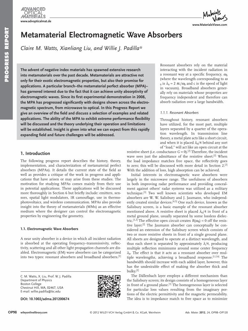
Figure 1 . Schematic of the two canonical metamaterial unit cells used to create magnetic and electric response. The split ring resonator (a) responds to electromagnetic waves with a Lorentz-type magnetic response of a wave polarized as shown in (d). The electric ring resonator (b) yields a resonant permittivity for radiation polarized as shown in (e). In (c) we show a magneto-electric unit cell consisting of an ERR from (b) combined with a metallic ground plane–polarization shown in (f). Squares shown in (a), (b) and (c) and cubes shown in (d), (e) and (f) represent the unit cell–cubic in these cases.
preventing health risks due to exposure of specifi c electromag-netic radiation at particular frequencies, this is also useful for wireless communication. Absorbers that serve this purpose have been made, for example, from nanomagnets and were shown to suffi ciently absorb millimeter waves. [ 15 ]
1.1.4. Kirchhoff ’s Law: Emitters and Absorbers
Thermal emitters are another type of EM wave absorber. Kirchhoff’s law states: “at a given temperature the ratio of the emitted power to the fraction of power absorbed is the same for all bodies, and is equal to the irradiance within a hollow cavity.” [ 16 ] Although studies generally focus on the emissive properties, due to Kirchhoff’s law, a perfect emitter is equiva-lent to a perfect absorber; this concept will be discussed more in Section 6 where we note MPAs usefulness as selective thermal emitters. These designs had their roots as early as 1977 when it was shown that ZnSe thin fi lms emitted radiation due to sur-face polaritons. [ 17 ] The concept extended to include gratings, [ 18 ] photonic crystals, [ 19 , 20 ] and subwavelength hole arrays. [ 21 , 22 ] This last design, in particular, is very similar to some metamaterial fi shnet designs that were later used as MPAs; it generally con-sists of a periodic hole array over a continuous ground plane surrounding a dielectric. [ 21 ] However, the goal of this progress report will be to focus on the more traditional MPAs, as will be discussed in Section 3. Section 6 will briefl y overview similar MPA geometries that were utilized for emitters.
1.2. Metamaterials
Electromagnetic metamaterials [ 23 , 24 ] are arrays of structured subwavelength elements which may be described as effective materials via ε ( ω ) and μ ( ω ), the electric permittivity and mag-netic permeability, respectively. Although initial interest in metamaterials arose due to their ability to exhibit exotic elec-tromagnetic effects impossible to achieve with natural mate-rial, they are excellent candidates for electromagnetic wave absorbers. For example, metamaterials have been shown able to achieve negative index of refraction–a phenomenon fi rst postu-lated by Veselago in 1968. [ 25 ] The theoretic background hinged on a material with simultaneously negative values of the ε and μ , hence giving an index of refraction, n = √
εr μr that is less than zero. [ 25 ] Veselago predicted the following exotic properties for materials with negative index: reverse Cerenkov radiation, reverse Doppler shift, and opposite phase and group velocity, among others. [ 25 ] The advent of Pendry’s artifi cial magnetism in 1999 [ 24 ] opened up possibilities to create negative index mate-rials. Pendry et al . postulated that by creating “artifi cial atoms” (i.e. artifi cially engineered, subwavelength structures) one could construct artifi cial materials to exhibit an effective per-mittivity and permeability. [ 24 ] Utilizing these shaped materials, called “split ring resonators,” along with a negative dielectric wire medium, a negative index of refraction was experimen-tally demonstrated. [ 26 , 27 ] Although this fi rst demonstration of negative index of refraction was carried out at microwave fre-quencies, it has since been demonstrated to operate from the radio frequency range to the optical realm. [ 27–33 ] In addition to negative refractive index, many other exotic applications
wileyonlinelibrary.com © 2012 WILEY-VCH Verlag G
of metamaterials were demonstrated including invisibility cloaking, [ 34 ] perfect lenses, [ 35 , 36 ] the hyperlens, [ 37 ] aberration free lenses, [ 38 ] and, as demonstrated in this progress report, meta-material perfect absorbers. [ 39 ]
Typically MM components are fashioned from highly con-ductive metals, such as copper, gold, or silver, and may be formed into periodic wire arrays or various types of split rings, similar to those used by Pendry in 1999. [ 24 ] Split rings may be formed into one unit cell, or may consist of several sub-units, and then arrayed to fi ll space in one, two and three dimensions. Two canonical metamaterial elements are shown in Figure 1 : in (a, d) the magnetic split ring resonator (SRR), and in (b, e) the electric ring resonator (ERR).
Metamaterials allow for the explicit design of the effective parameters ε ( ω ) and μ ( ω ); they can be described with standard electromagnetic theory, as will be demonstrated in Section 2. Using the two building blocks for magnetic (Figure 1 a) and electric (Figure 1 b) response, one may computationally design each independently, and then combine together. Undesirable electromagnetic interactions between unit cells may necessitate further optimization of the combined structure. The combined unit cell may then be used to build a material where the electro-magnetic properties of the resulting composite are completely described by the unit cell.
The SRR and ERR achieve a frequency dependent Drude-Lorentz type resonant response–as will be explained in Section 2, ( Equations 6 , 7 )–to incident time varying magnetic and elec-tric fi elds, respectively. Metamaterial elements may also yield a much more complicated bianisotropic [ 40 , 41 ] and/or spatially dis-persive response. [ 42 ]
Interactions between metamaterial elements may also be utilized to form both the electric and magnetic response. Figure 1 (c, f) shows a unit cell where an ERR is spaced a small distance from a continuous conducting ground plane. This unit cell achieves an electric Drude response from the ground plane plus a Drude-Lorentz response from the ERR. Magnetic response is achieved from currents which run in the ERR and in
mbH & Co. KGaA, Weinheim Adv. Mater. 2012, 24, OP98–OP120
PRO
GRES
S R
EPO
RT
www.MaterialsViews.comwww.advopticalmat.de
the ground plane. These currents are anti-parallel and thus the magnetic fi eld couples to them providing a Lorentz-like μ ( ω ). The electric response may be tuned by altering the geometry of the ERR, and the magnetic response is tuned by changing the spacing between the ERR and the ground plane. As will be shown in the following sections, this is the general mechanism behind the vast majority of MPAs demonstrated to date.
The single most salient feature exhibited by metamaterials is that, unlike naturally occurring materials, metamaterials achieve their electromagnetic properties from their geometry rather than their chemistry or band structure. To a rough approxima-tion, the wavelength associated with the metamaterial resonant frequency is proportional to the “unwound” length L of a SRR or ERR, i.e. λ 0 ∼ 2 L . As such, metamaterials may be fashioned to operate over all sub-optical frequencies by simple scaling of L –indeed RF, microwave, millimeter wave, terahertz, infrared, and near infrared examples have been demonstrated.
1.3. Metamaterial Perfect Absorber (MPA)
An absorber, based on a metamaterial high impedance surface, was postulated and consisted of an array of SRRs spaced a dis-tance above a ground plane and separated by a dielectric. [ 43 ] An incident wave would therefore have a refl ectivity of 1 and pro-duce large electric fi elds at the surface of the metamaterial. A resistive sheet placed on the outward surface of the MM could absorb this energy before refl ecting back. [ 43 ] Although this ful-fi lls the same needs as other current absorbers, such as the Salisbury Screen, [ 5 ] it has the benefi t of being thin. This original theoretical prediction requires the dielectric layer to be much thinner than the operational wavelength. [ 43 ]
Although the above design did utilize MMs to create an EM wave absorber, the absorption mechanism was not the same as some of the more traditional MPAs developed in the past three years, which this Progress Report will focus on. The fi rst exper-imental demonstration of such an MPA was in 2008 [ 39 ] and uti-lized a metamaterial 2D ERR structure over a cut wire medium separated by a dielectric layer. [ 39 ] This design also neglects the resistive sheet that is included in other designs; [ 43 ] the loss orig-inates in the dielectric layer. As mentioned above, the electric response derives from the top ERR structure and the magnetic response from anti-parallel currents in the top and bottom metal layers. [ 39 ] This seminal work in the microwave regime soon inspired work in other frequency regimes with high absorp-tivity being experimentally realized or numerically predicted in the THz regime in 2008, [ 44 ] MIR frequencies in 2010, [ 45 ] NIR frequencies in 2008, [ 46 ] and in the visible realm in 2011. [ 47 ] In Section 3, many designs will be discussed, including MPAs that are polarization insensitive, [ 48 ] can absorb radiation at wide inci-dent angles, [ 49 ] MPAs that exhibit absorption at more than one frequency band, [ 50 , 51 ] and dynamic MPAs. [ 52 ]
2. Theory
2.1. Electromagnetic Wave Absorption Theory
We begin by considering all possible ways in which electro-magnetic energy can propagate at an interface. Electromagnetic
© 2012 WILEY-VCH Verlag GAdv. Mater. 2012, 24, OP98–OP120
waves incident upon a boundary or surface may be refl ected, transmitted, absorbed, scattered, or may excite surface electro-magnetic waves (SEWs).
2.2. Wave Propagation
We only consider wavelengths in the range of λ 0 , and assume that the surface has an average roughness ( R a ) that is much smaller than the characteristic wavelength R a < < λ 0 , such that we may ignore scattering effects.
The surface may also support plasmons [ 53 ] or, more gener-ally, surface electromagnetic waves, [ 54–58 ] which may be explored by considering their propagation length, often described as L p = 1
2k2 , where k 2 is the imaginary portion of the complex
wavevector k‖ = k1 + ik2 , (SI units of 1/meters) and we are only considering the wavevector parallel to the surface. [ 59 ] Thus L p is the characteristic distance over which the intensity of the SEW or plasmon decays by 1/ e .
It is clear, however, that the plasmon propagation length L p is an insuffi cient description of what we would like to quantify which is “ how easy is it for an external electromagnetic wave to couple to a surface and then propagate as a SEW .” Our interest in this more specifi c question arises because surface waves may re-scatter before being absorbed, thus effectively being transmitted or refl ected. In order for an incident electromag-netic wave to couple to a surface wave, energy ( E = hω ) and momentum ( p = hk1 ) must be conserved, and thus we must have k 1 = k 0 , where k 1 is the real part of the wavevector in our medium and ω 0 = c k 0 , assuming we are at our wavelength of interest ω0 = 2π c
λ0 . We propose a fi gure of merit which encap-
sulates the above discussion and is defi ned as,
Wp = 1
2
k2
|k1 − k0|2 + k22 (1)
Obviously the fi gure of merit presented in Equation (1) takes into account how much our incident wavevector both matches the dispersion of our surface k 1 , and considers the loss k 2 of the surface for propagation of our SEW. Clearly W p reduces to L p if our momentum is perfectly matched k 1 = k 0 .
If k 2 is suffi ciently large, generation of surface electromag-netic waves may be a form of loss but, as mentioned, the SEW may re-radiate the wave if, e.g. our surface is curved. Thus assuming we have a fl at surface such that any SEWs or plas-mons die out before re-scattering, we may then fi nally resolve that a wave may be refl ected ( R ), transmitted ( T ), or absorbed ( A ), with their relationship given as A = 1– T – R .
2.3. Fresnel Equations
In what follows we consider two cases; (i) a slab of thickness d of magneto-dielectric medium described by both the mag-netic permeability μ(ω) = μ0μr (ω) and the electric permittivity ε(ω) = ε0εr (ω) and backed by a highly conductive opaque metallic ground plane, and (ii) a slab of thickness d of a magneto-dielectric medium { μ ( ω ) ε ( ω )} embedded in vacuum. Here ε 0 and μ 0 are the permittivity and permeability of free space, where the
OP101wileyonlinelibrary.commbH & Co. KGaA, Weinheim

OP102
PRO
GRES
S R
EPO
RT
www.MaterialsViews.comwww.advopticalmat.de
Figure 2 . (a) Absorptivity (red), transmissivity (blue), and refl ec-tivity (green) for a magneto-dielectric medium backed by a metallic ground plane. (b) Real (dark grey) and imaginary (light grey) portions of the permittivity and permeability of the magneto-dielectric material. (c) Absorptivity (red), transmissivity (blue), and refl ectivity (green) for a magneto-dielectric medium of thickness d .
permeability is μ 0 = 4 π × 10 − 7 Hm − 1 and the permittivity has a value of ε0 = 107
/4πc2Fm−1 . The relative permeability μr (ω)
and the relative permittivity εr (ω) are unitless and describe parameters normalized with respect to the free space values.
For Case (i) we begin by considering the refl ectivity ( R ) and refl ection coeffi cient ( r ) of an interface, for transverse electric (TE) and transverse magnetic (TM) polarized waves as,
RT E = |rT E |2 =∣∣∣∣∣cos θ − μ−1
r
√n2 − sin θ2
cos θ + μ−1r
√n2 − sin θ2
∣∣∣∣∣2
(2)
RT M = |rT M|2 =∣∣∣∣∣εr cos θ − √
n2 − sin θ2
εr cos θ + √n2 − sin θ2
∣∣∣∣∣2
(3)
where θ is the angle of incidence, and n = √μr εr is the index
of refraction of the magneto-dielectric medium. If we restrict our incident electromagnetic wave to normal, i.e. θ = 0 ° , Equa-tions (2 ), (3) reduce to,
R =
∣∣∣∣ Z − Z0
Z + Z0
∣∣∣∣2
=∣∣∣∣μr − n
μr + n
∣∣∣∣2
(4)
where Z = √μ/ε is the impedance of the magneto-dielectric
material and Z0 = √μ0/ε0 is the impedance of free space. For
Case (i) the metallic ground plane provides a zero transmis-sivity and it might be tempting to write for the absorptivity,
A = 1 − R = 1 −∣∣∣∣ Z − Z0
Z + Z0
∣∣∣∣2
= 1 −∣∣∣∣μr − n
μr + n
∣∣∣∣2
(5) However, as mentioned, our impedance matched condi-
tion above is only valid for the refl ectivity of an interface and thus incident radiation may still be transmitted through the medium. If our material is not of suffi cient thickness ( d ) and loss ( k 2 ) then the wave will be refl ected from the conducting metallic plane and may be refl ected back into free space.
2.4. Transmission Matrix
A full treatment of Case (i) can be explored by considering a transmission matrix approach. We don’t list the full equations for the refl ectivity and transmissivity here, but simply point to one particular reference where this has been explicitly written out. [ 60 ] We study a three layer problem where an electromag-netic wave is incident from free space onto a magneto-dielectric medium of thickness d , described by the Drude-Lorentz model,
εr (ω) = ε∞ + ω2
p
ω20 − ω2 − iγeω (6)
μr (ω) = μ∞ + ω2
p,m
ω20,m − ω2 − iγmω (7)
where ω p , ω p,m are the plasma frequencies, ω 0 , ω 0,m are the center frequencies of the oscillator, γ e , γ m are the damping
wileyonlinelibrary.com © 2012 WILEY-VCH Verlag G
frequencies and ε ∞ , μ ∞ are the static permittivity and perme-ability at infi nite frequency, respectively. Here subscripted “ m’s ” refer to parameters for the permeability. We use, for our mag-neto-dielectric material, the parameters of ε(ω) = μ(ω) and we take ω p = 2 π × 1.25 THz, ω 0 = 2 π × 1.0 THz, γ = 2 π × 0.1 THz, and ε ∞ = 1.0. For our third opaque metallic layer we use the Drude parameters for gold ω p = 2 π × 2175 THz, ω 0 = 0, γ = 2 π × 6.5 THz, and ε ∞ = 1.0. [ 61 ]
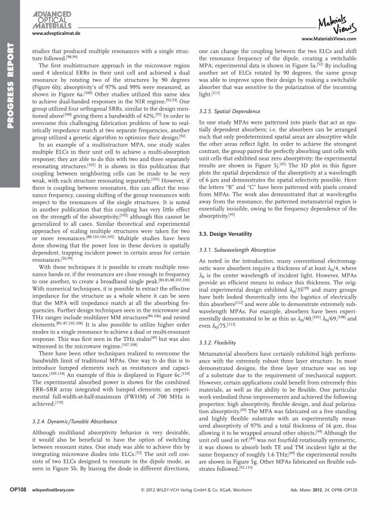
In Figure 2 a we plot results of Case (i): the refl ectivity (green curve), transmissivity (blue curve), and the absorp-tivity (red curve); in Figure 2 b the magneto-dielectric Lorentz oscillator layer described by Equations (6) ,( 7 ) is shown. As can be observed T is zero everywhere, but R is only small in the vicinity of where our Lorentz oscillator is centered, i.e.
mbH & Co. KGaA, Weinheim Adv. Mater. 2012, 24, OP98–OP120
PRO
GRES
S R
EPO
RT
www.MaterialsViews.comwww.advopticalmat.de
ω 0 = 2 π × 1.0 THz, and thus the absorptivity is near unity A ( ω 0 ) = 99.99% only in this regime.
The ‘narrow band’ absorptive behavior mentioned above can be understood by considering the penetration depth, [ 62 ]
δ = 1
2k2 (8)
which is similar to the plasmon propagation length L p , and thus describes the distance in which the intensity of electromagnetic radiation falls off to 1/ e . Here, since our electric and magnetic resonators are identical, we may write the complex wavevector as, k⊥ = ω
c n = ω
c εr , where we only consider wavevectors per-pendicular to the surface. It is useful to consider the real and imaginary portions of a Lorentz oscillator ( Equation 6 ),
ε(ω) = ε1r (ω) + iε2r (ω)
= ε∞ + ω2p
(ω2
0 − ω2)
(ω2
0 − ω2)2 + (γeω)2
+ iω2
pγeω(ω2
0 − ω2)2 + (γeω)2
(9) The penetration depth, and thus the loss, of our fi ctitious
magneto-dielectric material is given by δ = c2ωε2r
Thus fi nally we see that our metallic backed magneto-dielectric medium can only absorb a narrow range of frequencies near where the loss of our Lorentz oscillator peaks, see the light grey curve of Figure 2 b.
The second scenario–Case (ii)–we will consider is a magneto-dielectric material of thickness d embedded in vacuum. The refl ec-tion and transmission coeffi cients for this medium are given by,
r = − i
2
(Zr − Z−1
r
)sin (nkd) t
(10)
t =
[cos (nkd) − i
2
(Zr + Z−1
r
)sin (nkd)
]−1
(11)
where Z r = Z / Z 0 is the relative impedance of the medium. The refl ectivity and transmissivity are then simply given by,
R = |r |2 (12)
T = |t|2 (13)
© 2012 WILEY-VCH Verlag G
Figure 3 . The absorptivity for Case (i) as a function of frequency and thickSection 2). The right side of Equation (17) is plotted in (b) as a function oin (a), except each curve is for a different damping frequency. The grey por Equation (17) . In panel (c) the absorber thickness is plotted as a function o
Adv. Mater. 2012, 24, OP98–OP120
We use the same parameters for the magneto-dielectric mate-rial as in Case (i). Since our material is perfectly matched to free space our equations for the transmissivity and refl ectivity reduce to,
R = 0 (14)
T = e−2k2d = e−2n2ωd/c (15) In Figure 2 c we plot the refl ectivity, transmissivity, and
absorptivity, as the green, blue and red curves respectively. As can be observed, the refl ectivity is zero everywhere and the absorptivity reaches near unity values A ( ω 0 ) = 99.3%.
The absorptivity explored in both Case (i) and (ii) is narrow band but is able to reach maximal values with the use of lossy materials. Outside of this band the electromagnetic energy is either refl ected, as in Case (i), or transmitted–Case (ii); notice that R and T are essentially swapped between Figure 1 a and c.
2.5. Thickness and Loss Dependence
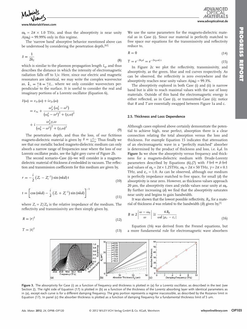
Although cases explored above certainly demonstrate the poten-tial to achieve high, near perfect, absorption there is a clear connection relating the total absorption versus the loss and thickness. For example Equation 15 indicates that attenuation of an electromagnetic wave in a “perfectly matched” absorber is determined by the product of thickness and loss, i.e. k 2 d . In Figure 3 a we show the absorptivity versus frequency and thick-ness for a magneto-dielectric medium with Drude-Lorentz parameters described by Equations (6) ,( 7 ) with ε (ω) = μ (ω) and values of ω p = 2 π × 1.25THz, ω 0 = 2 π × 50 THz, γ = 2 π × 0.1 THz, and ε ∞ = 1.0. As can be observed, although our medium is perfectly impedance matched to free space, for small ( d ) the absorptivity is near zero. However, as thickness values approach 20 μ m, the absorptivity rises and yields values near unity at ω 0 . By further increasing ( d ) we fi nd that the absorptivity saturates near unity and begins to gain bandwidth.
It was shown that the lowest possible refl ectivity, R 0 , for a mate-rial of thickness d was related to the bandwidth ( B ) given by, [ 1 ]
B ≡ 2
∣∣∣∣ω − ω0
ω
∣∣∣∣ ∼= 4R0
ωd |μr − εr | (16)
Equation (16) was derived from the Fresnel equations, but a more fundamental rule for electromagnetic wave absorbers
OP103wileyonlinelibrary.commbH & Co. KGaA, Weinheim
ness is plotted in (a) for a Lorentz oscillator, as described in the text (see f the thickness of the Lorentz absorbing layer with identical parameters as tion represents a regime inaccessible, as described by the Rozanov limit in f damping frequency for a fundamental thickness limit of 5 um.

OP104
PRO
GRES
S R
EPO
RT
www.MaterialsViews.comwww.advopticalmat.de
results from the Kramers-Kronig (KK) relations [ 63 , 64 ] and dic-tates that a wider absorptive bandwidth requires materials with larger thicknesses. The fundamental relationship for the absorptivity bandwidth and the thickness, valid for any single layer metal backed magneto-dielectric absorber at normal inci-dence, is, [ 65 , 66 ]
DR ≥ 1
2π 2μs
∣∣∣∣∫ ∞
0ln |r (λ)| dλ
∣∣∣∣ ≡ dR (17)
where μ s is the static permeability, i.e. μ at zero frequency. For multiple layers the product μ s D R must be summed over all sur-faces. As the limit of thickness described in Equation (16) is based on causality, i.e. KK, the conditions are very general and include all passive linear, reciprocal and causal materials.
Figure 3 b plots the right side of Equation (17) , i.e. d R , as a function of the actual thickness D R of an absorber for Case (i), (with the parameters for a Lorentz oscillator with ε (ω) = μ (ω) of ω p = 2 π × 1.25 THz, ω 0 = 2 π × 50 THz, and ε ∞ = 1.0), for different values of the scattering frequency γ . Since Equation (17) places a lower bound on the thickness of an absorber, for a given bandwidth, all curves must lie in the non-shaded region of Figure 3 b. For relatively high values of γ the curves do not approach the limit of Equation (17) . However, as γ is lowered the thickness of the absorbers approaches the fundamental limit.
We plot, in Figure 3 c, the absorber thickness D R as a function of damping frequency for the case of a fundamental thickness limit of d R = 5 μ m. As can be observed the lower the scattering frequency γ the closer we are able to approach the theoretical limit. The analysis presented here thus suggest that in order to achieve the ultimate bandwidth to thickness ratio, one should use high quality factor Lorentz resonances in ε ( ω ) and μ ( ω ), where the quality factor for a Lorentz oscillator is defi ned as,
Q = ω0
γ (18) Metamaterials, as laid out in Section 1, can be described by
the above theory and represented by effective optical constants (i.e. ε ( ω ) and μ ( ω )). The physical mechanism behind the MPA will be explained more thoroughly in the Section 3, although the refl ectivity, transmissivity, and absorption properties can be understood from the above analysis. As has been stated, the general idea is to minimize refl ection off the metamaterial surface and then, utilizing such factors as thickness and other material properties, create loss to give high absorptivity.
3. Current State of the Art
In the following, we overview current work in the fi eld of meta-material perfect absorbers. Section 3.1 begins with a descrip-tion of the fi rst metamaterial perfect absorber, carried out at microwave frequencies, and follows with a discussion of demonstrated designs at millimeter waves, THz, infrared, and optical wavelengths. Although there is no standard terminology for the various ranges of the electromagnetic spectrum, for the purposes of this section we take the common defi nition of: microwave (1 GHz–30 GHz: 30 cm–10 mm), millimeter wave
wileyonlinelibrary.com © 2012 WILEY-VCH Verlag G
(30 GHz–300 GHz: 10 mm–1 mm), THz (300 GHz–10 THz: 1 mm–30 μ m), MIR (10 THz–100 THz: 30 μ m–3 μ m), NIR (100 THz–400 THz: 3 μ m–0.75 μ m), and visible (400 THz–800 THz: 0.75 μ m–375 nm).
The rest of this section is dedicated to describing various major topics which have driven the fi eld of metamaterial per-fect absorbers. The MPA design is extremely versatile thus per-mitting great fl exibility in performance; Section 3.2 will discuss the main trends in designing MPAs: 3.2.1 polarization inde-pendent, 3.2.2 broad angle, 3.2.3 broad band, 3.2.4 dynamic and 3.2.5 spatially dependent MPAs. The design parameters of MPAs are also versatile, Section 3.3 will highlight ways in which MPAs have been able to utilize their design to better their per-formance: 3.3.1 sub-wavelength thickness, 3.3.2 fl exible sub-strate, and 3.3.3 three-dimensional design. Finally, Sections 3.4 and 3.5 will look at some of the alternative approaches to EM wave absorption. These will include both MPAs that utilize a different operational mechanism and absorbers which are sim-ilar to, but diffi cult to defi ne as, metamaterial based absorbers.
3.1. Metamaterial Perfect Absorbers
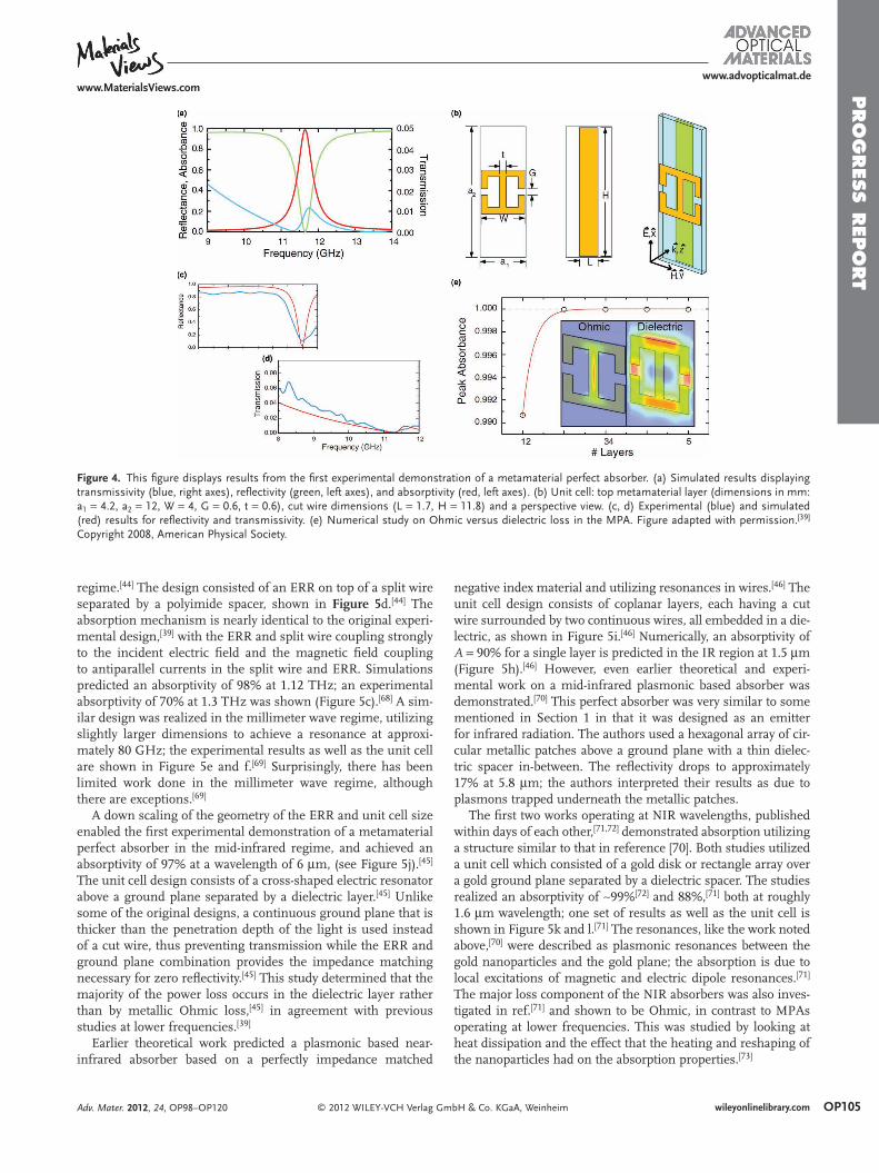
The fi rst metamaterial based absorber by Landy et al. [ 39 ] utilizes three layers, two metallic layers and a dielectric, and demon-strated a simulated absorptivity of A ≈ 99% at 11.48 GHz, as shown in Figure 4 a. [ 39 ] The top layer consists of an ERR which provides, along with the ground plane, the electric response by coupling strongly to incident electric fi eld at a certain resonance frequency. The second metal, spaced apart from the top layer by a dielectric, consists of a cut wire in a parallel plane and also contributes to the electric response, see Figure 4 b. Magnetic coupling is achieved via antiparallel currents in the cut wire and the center wire of the ERR. An incident time varying magnetic fi eld may couple to these antiparallel currents, thus yielding a Lorentz like magnetic response. The combined design allows for individual tuning of the electric and magnetic responses. For example, adjustment of the geometry of the ERR permits tuning the frequency position and strength of a Lorentz reso-nance, while altering the spacing of the two metallic structures, and their geometry, allows the magnetic response to be modi-fi ed. In reference [ 39 ] all three layers were fabricated with PCB using photosensitized FR4–a common method for fabrication of metamaterials operating in the microwave frequency range, as will be discussed in Section 4.
Experimentally, Landy et. al. was able to achieve an absorp-tivity of 88% (Figure 4 c,d). The authors postulated that dis-crepancies between simulated and measured results were due to fabrication errors. Additionally, the same study investigated loss mechanisms in their structure through simulations. It was found that dielectric loss occurring between the two MM layers far exceeded the Ohmic loss and was mainly concentrated in the center of the metamaterial unit cell beneath the strip of the ERR, as seen in Figure 4 e. [ 39 ] The authors determined by simu-lations that dielectric loss was an order of magnitude greater than Ohmic loss. The primary loss mechanism for most struc-tures in the microwave region is through the dielectric. [ 39 , 67 ]
Although the fi rst experimental work on MPAs was in the microwave frequency realm, work quickly followed in the THz
mbH & Co. KGaA, Weinheim Adv. Mater. 2012, 24, OP98–OP120
PRO
GRES
S R
EPO
RT
www.MaterialsViews.comwww.advopticalmat.de
Figure 4 . This fi gure displays results from the fi rst experimental demonstration of a metamaterial perfect absorber. (a) Simulated results displaying transmissivity (blue, right axes), refl ectivity (green, left axes), and absorptivity (red, left axes). (b) Unit cell: top metamaterial layer (dimensions in mm: a 1 = 4.2, a 2 = 12, W = 4, G = 0.6, t = 0.6), cut wire dimensions (L = 1.7, H = 11.8) and a perspective view. (c, d) Experimental (blue) and simulated (red) results for refl ectivity and transmissivity. (e) Numerical study on Ohmic versus dielectric loss in the MPA. Figure adapted with permission. [ 39 ] Copyright 2008, American Physical Society.
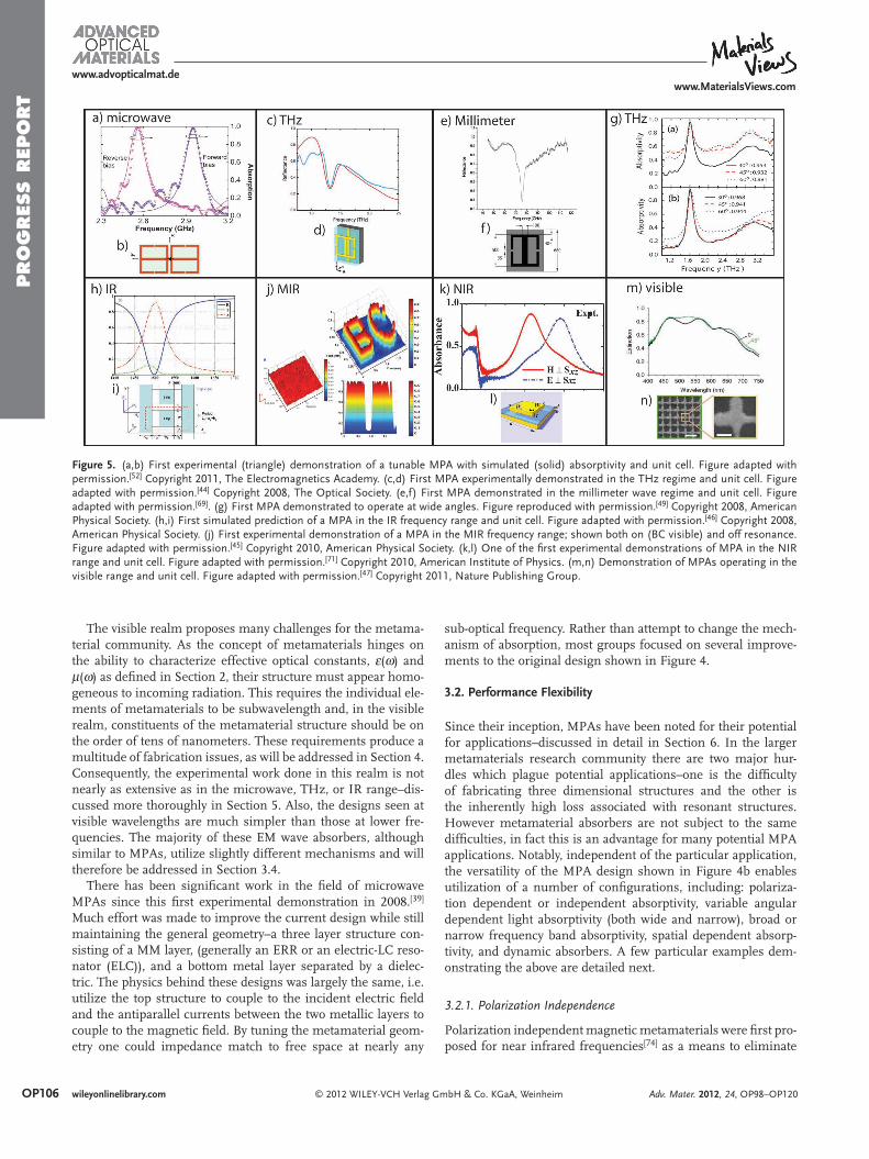
regime. [ 44 ] The design consisted of an ERR on top of a split wire separated by a polyimide spacer, shown in Figure 5 d. [ 44 ] The absorption mechanism is nearly identical to the original experi-mental design, [ 39 ] with the ERR and split wire coupling strongly to the incident electric fi eld and the magnetic fi eld coupling to antiparallel currents in the split wire and ERR. Simulations predicted an absorptivity of 98% at 1.12 THz; an experimental absorptivity of 70% at 1.3 THz was shown (Figure 5 c). [ 68 ] A sim-ilar design was realized in the millimeter wave regime, utilizing slightly larger dimensions to achieve a resonance at approxi-mately 80 GHz; the experimental results as well as the unit cell are shown in Figure 5 e and f. [ 69 ] Surprisingly, there has been limited work done in the millimeter wave regime, although there are exceptions. [ 69 ]
A down scaling of the geometry of the ERR and unit cell size enabled the fi rst experimental demonstration of a metamaterial perfect absorber in the mid-infrared regime, and achieved an absorptivity of 97% at a wavelength of 6 μ m, (see Figure 5 j). [ 45 ] The unit cell design consists of a cross-shaped electric resonator above a ground plane separated by a dielectric layer. [ 45 ] Unlike some of the original designs, a continuous ground plane that is thicker than the penetration depth of the light is used instead of a cut wire, thus preventing transmission while the ERR and ground plane combination provides the impedance matching necessary for zero refl ectivity. [ 45 ] This study determined that the majority of the power loss occurs in the dielectric layer rather than by metallic Ohmic loss, [ 45 ] in agreement with previous studies at lower frequencies. [ 39 ]
Earlier theoretical work predicted a plasmonic based near-infrared absorber based on a perfectly impedance matched
© 2012 WILEY-VCH Verlag GAdv. Mater. 2012, 24, OP98–OP120
negative index material and utilizing resonances in wires. [ 46 ] The unit cell design consists of coplanar layers, each having a cut wire surrounded by two continuous wires, all embedded in a die-lectric, as shown in Figure 5 i. [ 46 ] Numerically, an absorptivity of A = 90% for a single layer is predicted in the IR region at 1.5 μ m (Figure 5 h). [ 46 ] However, even earlier theoretical and experi-mental work on a mid-infrared plasmonic based absorber was demonstrated. [ 70 ] This perfect absorber was very similar to some mentioned in Section 1 in that it was designed as an emitter for infrared radiation. The authors used a hexagonal array of cir-cular metallic patches above a ground plane with a thin dielec-tric spacer in-between. The refl ectivity drops to approximately 17% at 5.8 μ m; the authors interpreted their results as due to plasmons trapped underneath the metallic patches.
The fi rst two works operating at NIR wavelengths, published within days of each other, [ 71 , 72 ] demonstrated absorption utilizing a structure similar to that in reference [ 70 ] . Both studies utilized a unit cell which consisted of a gold disk or rectangle array over a gold ground plane separated by a dielectric spacer. The studies realized an absorptivity of ∼ 99% [ 72 ] and 88%, [ 71 ] both at roughly 1.6 μ m wavelength; one set of results as well as the unit cell is shown in Figure 5 k and l. [ 71 ] The resonances, like the work noted above, [ 70 ] were described as plasmonic resonances between the gold nanoparticles and the gold plane; the absorption is due to local excitations of magnetic and electric dipole resonances. [ 71 ] The major loss component of the NIR absorbers was also inves-tigated in ref. [ 71 ] and shown to be Ohmic, in contrast to MPAs operating at lower frequencies. This was studied by looking at heat dissipation and the effect that the heating and reshaping of the nanoparticles had on the absorption properties. [ 73 ]
OP105wileyonlinelibrary.commbH & Co. KGaA, Weinheim
OP106
PRO
GRES
S R
EPO
RT
www.MaterialsViews.comwww.advopticalmat.de
Figure 5 . (a,b) First experimental (triangle) demonstration of a tunable MPA with simulated (solid) absorptivity and unit cell. Figure adapted with permission. [ 52 ] Copyright 2011, The Electromagnetics Academy. (c,d) First MPA experimentally demonstrated in the THz regime and unit cell. Figure adapted with permission. [ 44 ] Copyright 2008, The Optical Society. (e,f) First MPA demonstrated in the millimeter wave regime and unit cell. Figure adapted with permission. [ 69 ] . (g) First MPA demonstrated to operate at wide angles. Figure reproduced with permission. [ 49 ] Copyright 2008, American Physical Society. (h,i) First simulated prediction of a MPA in the IR frequency range and unit cell. Figure adapted with permission. [ 46 ] Copyright 2008, American Physical Society. (j) First experimental demonstration of a MPA in the MIR frequency range; shown both on (BC visible) and off resonance. Figure adapted with permission. [ 45 ] Copyright 2010, American Physical Society. (k,l) One of the fi rst experimental demonstrations of MPA in the NIR range and unit cell. Figure adapted with permission. [ 71 ] Copyright 2010, American Institute of Physics. (m,n) Demonstration of MPAs operating in the visible range and unit cell. Figure adapted with permission. [ 47 ] Copyright 2011, Nature Publishing Group.
The visible realm proposes many challenges for the metama-terial community. As the concept of metamaterials hinges on the ability to characterize effective optical constants, ε ( ω ) and μ ( ω ) as defi ned in Section 2, their structure must appear homo-geneous to incoming radiation. This requires the individual ele-ments of metamaterials to be subwavelength and, in the visible realm, constituents of the metamaterial structure should be on the order of tens of nanometers. These requirements produce a multitude of fabrication issues, as will be addressed in Section 4. Consequently, the experimental work done in this realm is not nearly as extensive as in the microwave, THz, or IR range–dis-cussed more thoroughly in Section 5. Also, the designs seen at visible wavelengths are much simpler than those at lower fre-quencies. The majority of these EM wave absorbers, although similar to MPAs, utilize slightly different mechanisms and will therefore be addressed in Section 3.4.
There has been signifi cant work in the fi eld of microwave MPAs since this fi rst experimental demonstration in 2008. [ 39 ] Much effort was made to improve the current design while still maintaining the general geometry–a three layer structure con-sisting of a MM layer, (generally an ERR or an electric-LC reso-nator (ELC)), and a bottom metal layer separated by a dielec-tric. The physics behind these designs was largely the same, i.e. utilize the top structure to couple to the incident electric fi eld and the antiparallel currents between the two metallic layers to couple to the magnetic fi eld. By tuning the metamaterial geom-etry one could impedance match to free space at nearly any
wileyonlinelibrary.com © 2012 WILEY-VCH Verlag G
sub-optical frequency. Rather than attempt to change the mech-anism of absorption, most groups focused on several improve-ments to the original design shown in Figure 4 .
3.2. Performance Flexibility
Since their inception, MPAs have been noted for their potential for applications–discussed in detail in Section 6. In the larger metamaterials research community there are two major hur-dles which plague potential applications–one is the diffi culty of fabricating three dimensional structures and the other is the inherently high loss associated with resonant structures. However metamaterial absorbers are not subject to the same diffi culties, in fact this is an advantage for many potential MPA applications. Notably, independent of the particular application, the versatility of the MPA design shown in Figure 4 b enables utilization of a number of confi gurations, including: polariza-tion dependent or independent absorptivity, variable angular dependent light absorptivity (both wide and narrow), broad or narrow frequency band absorptivity, spatial dependent absorp-tivity, and dynamic absorbers. A few particular examples dem-onstrating the above are detailed next.
3.2.1. Polarization Independence
Polarization independent magnetic metamaterials were fi rst pro-posed for near infrared frequencies [ 74 ] as a means to eliminate
mbH & Co. KGaA, Weinheim Adv. Mater. 2012, 24, OP98–OP120
PRO
GRES
S R
EPO
RT
www.MaterialsViews.comwww.advopticalmat.de
bianisotropy [ 75 ] by appealing to racemic mixtures of unit cells. [ 76 , 77 ] Electric metamaterials were also proposed for both polarization dependent [ 78 ] and polarization independent dielec-tric response. [ 79 ] A metamaterial unit cell consisting of ERRs similar to that in ref. [ 79 ] combined with a cross demonstrated polarization insensitive absorptivity at THz frequencies. [ 48 ]
Other designs also achieved polarization independent absorptivity by utilizing structures with four fold rotational sym-metry. [ 80 , 81 ] One study featured equal combinations of polariza-tion sensitive unit cells rotated by 90 degrees with respect to each other. [ 81 ] The unit cell consisted of four primitive cells and thus was four-fold rotationally symmetric. All metamaterials mentioned above achieve electromagnetic absorptivity with unpolarized light using unit cells with π /2 rotation symmetry. However, it was demonstrated that approximate polarization independent absorptivity was possible by utilizing an asym-metric unit cell: it absorbed both when the electric fi eld was across the ERR gaps via the standard ERR resonance and also along the gaps through nearest neighbor interactions giving rise to capacitive effects. [ 82 ] In this case, as the unit cell did not have π /2 symmetry, the absorptivity was achieved in multiple polarization modes through a different mechanism. [ 82 ]
Another work proposed that chiral metamaterials could achieve polarization independent absorption. [ 83 ] Rather than the standard 3-layer design, this group utilized a chiral version of an SRR that consisted of two stacked rings connected by vias to create an inductive effect, while strips of these chiral meta-materials are then interlocked in a 3D grid to create a capacitive effect; the chiral metamaterial array is then backed by a copper ground plane and covered with a dielectric plate. [ 83 ]
Since these fi rst few absorbers many groups have also shown absorption for all wave polarizations using very similar struc-tures in various bands of the electromagnetic spectrum, such as at THz [ 84–89 ] and IR. [ 72 , 71 , 90–94 ] Many plasmonic absorbers yield polarization independent response, as the structures uti-lized are either rotationally symmetric, or have π /2 rotational symmetry. [ 70 , 72 ]
3.2.2. Broad Angle
For nearly all metamaterial absorber designs based upon the canonical three layer geometry, (shown in Figure 4 b), the dependence of the absorptivity as a function of incident angle for both TE and TM polarizations was explored for both two
© 2012 WILEY-VCH Verlag G
Figure 6 . (a,b) One of the fi rst MPAs to utilize a multistructure design: exp2010, The Electromagnetics Academy. (c) MPA utilizing lumped elements (u2010, American Institute of Physics. (d,e) MPA utilizing single structure wpermission. [ 51 ] Copyright 2010, Institute of Physics.
Adv. Mater. 2012, 24, OP98–OP120
and four fold symmetric unit cells. Many of the MPA designs are able to absorb light at a high angle of incidence in the microwave, [ 81–83 , 94 , 95 ] IR, [ 46 , 71–73 , 90 , 92 , 93 , 96 ] and THz. [ 49 , 84 , 85 , 87–
89 ] The majority of these can absorb for both TE and TM modes. [ 71 , 72 , 82 , 90 , 92–94 ] The fi rst computational and experimental study detailing the ability of the MPA to absorb a wide inci-dent angle of radiation showed numerically that the absorp-tivity remains above 99% for TM polarizations less than 80 ° incidence, and stays above 90% for angles below 50 ° incidence for TE polarization. [ 49 ] Most of the studies noted here observe a monotonic decrease in the absorptivity at resonance for TE modes as a function of incidence angle for those above roughly 40 ° , whereas there was little change for the TM mode–at least below ∼ 80 ° . It was stated in multiple studies that this is due to the fact that, as the incident angle increases, the parallel mag-netic fi eld component approaches zero and thus can no longer effectively induce antiparallel currents in the top MM layer and the back metal structure resulting in a drop in the magnetic fl ux. [ 81 , 94 , 97 ]
3.2.3. Broad Bandwidth
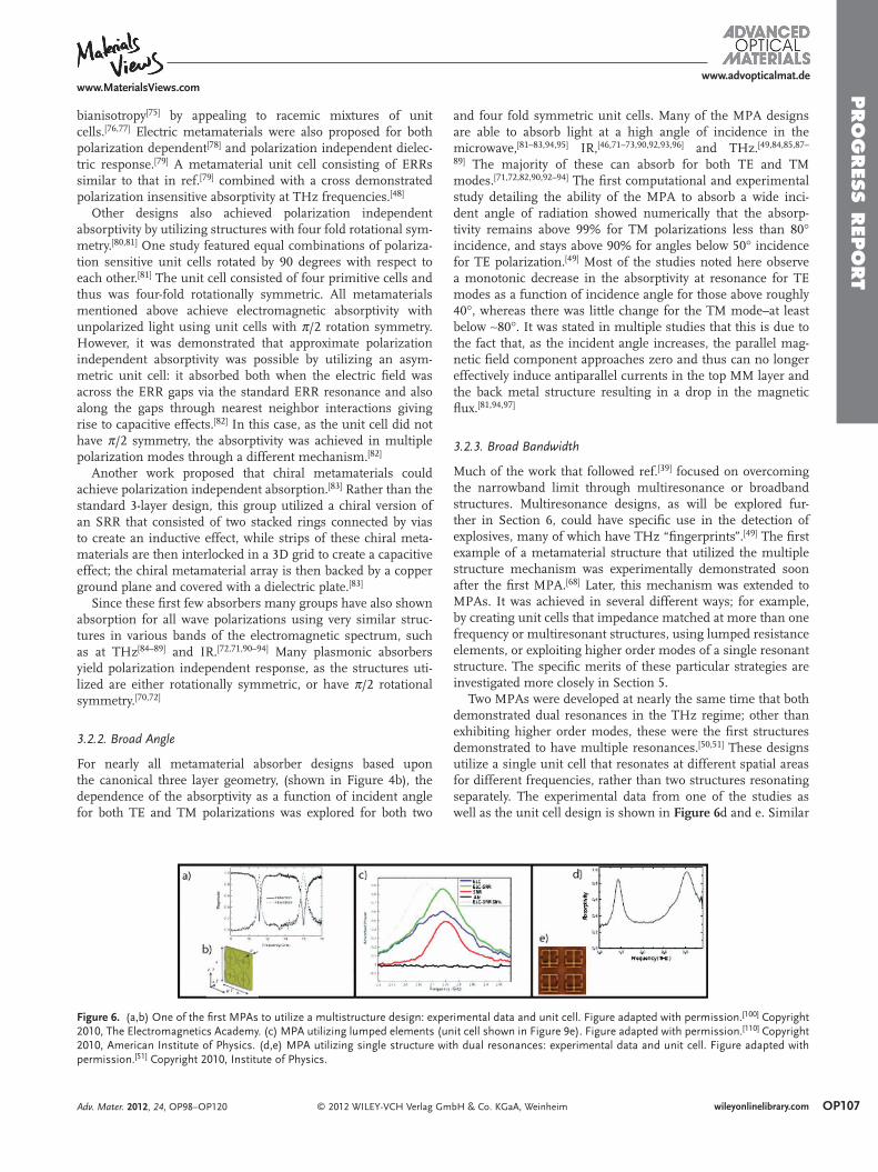
Much of the work that followed ref. [ 39 ] focused on overcoming the narrowband limit through multiresonance or broadband structures. Multiresonance designs, as will be explored fur-ther in Section 6, could have specifi c use in the detection of explosives, many of which have THz “fi ngerprints”. [ 49 ] The fi rst example of a metamaterial structure that utilized the multiple structure mechanism was experimentally demonstrated soon after the fi rst MPA. [ 68 ] Later, this mechanism was extended to MPAs. It was achieved in several different ways; for example, by creating unit cells that impedance matched at more than one frequency or multiresonant structures, using lumped resistance elements, or exploiting higher order modes of a single resonant structure. The specifi c merits of these particular strategies are investigated more closely in Section 5.
Two MPAs were developed at nearly the same time that both demonstrated dual resonances in the THz regime; other than exhibiting higher order modes, these were the fi rst structures demonstrated to have multiple resonances. [ 50 , 51 ] These designs utilize a single unit cell that resonates at different spatial areas for different frequencies, rather than two structures resonating separately. The experimental data from one of the studies as well as the unit cell design is shown in Figure 6 d and e. Similar
OP107wileyonlinelibrary.commbH & Co. KGaA, Weinheim
erimental data and unit cell. Figure adapted with permission. [ 100 ] Copyright nit cell shown in Figure 9 e). Figure adapted with permission. [ 110 ] Copyright ith dual resonances: experimental data and unit cell. Figure adapted with
OP108
PRO
GRES
S R
EPO
RT
www.MaterialsViews.comwww.advopticalmat.de
studies that produced multiple resonances with a single struc-ture followed. [ 98 , 99 ]
The fi rst multistructure approach in the microwave region used 4 identical ERRs in their unit cell and achieved a dual resonance by rotating two of the structures by 90 degrees (Figure 6 b); absorptivity’s of 97% and 99% were measured, as shown in Figure 6 a. [ 100 ] Other studies utilized this same idea to achieve dual-banded responses in the NIR regime. [ 92 , 93 ] One group utilized four orthogonal SRRs, similar to the design men-tioned above [ 100 ] giving them a bandwidth of 42%. [ 93 ] In order to overcome this challenging fabrication problem of how to real-istically impedance match at two separate frequencies, another group utilized a genetic algorithm to optimize their design. [ 92 ]
In an example of a multistructure MPA, one study scales multiple ELCs in their unit cell to achieve a multi-absorption response; they are able to do this with two and three separately resonating structures. [ 101 ] It is shown in this publication that coupling between neighboring cells can be made to be very weak, with each structure resonating separately. [ 101 ] However, if there is coupling between resonators, this can affect the reso-nance frequency, causing shifting of the group resonances with respect to the resonances of the single structures. It is noted in another publication that this coupling has very little effect on the strength of the absorptivity; [ 102 ] although this cannot be generalized to all cases. Similar theoretical and experimental approaches of scaling multiple structures were taken for two or more resonances. [ 88 , 103 , 104 , 105 ] Multiple studies have been done showing that the power loss in these devices is spatially dependent, trapping incident power in certain areas for certain resonances. [ 50 , 99 ]
With these techniques it is possible to create multiple reso-nance bands or, if the resonances are close enough in frequency to one another, to create a broadband single peak. [ 84 , 85 , 88 , 103 , 104 ] With numerical techniques, it is possible to extract the effective impedance for the structure as a whole where it can be seen that the MPA will impedance match at all the absorbing fre-quencies. Further design techniques seen in the microwave and THz ranges include multilayer MM structures [ 84 , 106 ] and nested elements. [ 85–87 , 102 , 106 ] It is also possible to utilize higher order modes in a single resonance to achieve a dual or multi-resonant response. This was fi rst seen in the THz realm [ 49 ] but was also witnessed in the microwave regime. [ 107 , 108 ]
There have been other techniques realized to overcome the bandwidth limit of traditional MPAs. One way to do this is to introduce lumped elements such as resistances and capaci-tances. [ 109 , 110 ] An example of this is displayed in Figure 6 c. [ 110 ] The experimental absorbed power is shown for the combined ERR–SRR array integrated with lumped elements; an experi-mental full-width-at-half-maximum (FWHM) of 700 MHz is achieved. [ 110 ]
3.2.4. Dynamic/Tunable Absorbance
Although multiband absorptivity behavior is very desirable, it would also be benefi cial to have the option of switching between resonant states. One study was able to achieve this by integrating microwave diodes into ELCs. [ 52 ] The unit cell con-sists of two ELCs designed to resonate in the dipole mode, as seen in Figure 5 b. By biasing the diode in different directions,
wileyonlinelibrary.com © 2012 WILEY-VCH Verlag G
one can change the coupling between the two ELCs and shift the resonance frequency of the dipole, creating a switchable MPA; experimental data is shown in Figure 5 a. [ 52 ] By including another set of ELCs rotated by 90 degrees, the same group was able to improve upon their design by making a switchable absorber that was sensitive to the polarization of the incoming light. [ 111 ]
3.2.5. Spatial Dependence
In one study MPAs were patterned into pixels that act as spa-tially dependent absorbers; i.e. the absorbers can be arranged such that only predetermined spatial areas are absorptive while the other areas refl ect light. In order to achieve the strongest contrast, the group paired the perfectly absorbing unit cells with unit cells that exhibited near zero absorptivity; the experimental results are shown in Figure 5 j. [ 45 ] The 3D plot in this fi gure plots the spatial dependence of the absorptivity at a wavelength of 6 μ m and demonstrates the spatial selectivity possible. Here the letters “B” and “C” have been patterned with pixels created from MPAs. The work also demonstrated that at wavelengths away from the resonance, the patterned metamaterial region is essentially invisible, owing to the frequency dependence of the absorptivity. [ 45 ]
3.3. Design Versatility
3.3.1. Subwavelength Absorption
As noted in the introduction, many conventional electromag-netic wave absorbers require a thickness of at least λ 0 /4, where λ 0 is the center wavelength of incident light. However, MPAs provide an effi cient means to reduce this thickness. The orig-inal experimental design exhibited λ 0 /35 [ 39 ] and many groups have both looked theoretically into the logistics of electrically thin absorbers [ 112 ] and were able to demonstrate extremely sub-wavelength MPAs. For example, absorbers have been experi-mentally demonstrated to be as thin as λ 0 /40, [ 101 ] λ 0 /69, [ 108 ] and even λ 0 /75. [ 113 ]
3.3.2. Flexibility
Metamaterial absorbers have certainly exhibited high perform-ance with the extremely robust three layer structure. In most demonstrated designs, the three layer structure was on top of a substrate due to the requirement of mechanical support. However, certain applications could benefi t from extremely thin materials, as well as the ability to be fl exible. One particular work embodied these improvements and achieved the following properties: high absorptivity, fl exible design, and dual polariza-tion absorptivity. [ 49 ] The MPA was fabricated on a free standing and highly fl exible substrate with an experimentally meas-ured absorptivity of 97% and a total thickness of 16 μ m, thus allowing it to be wrapped around other objects. [ 49 ] Although the unit cell used in ref. [ 49 ] was not fourfold rotationally symmetric, it was shown to absorb both TE and TM incident light at the same frequency of roughly 1.6 THz; [ 49 ] the experimental results are shown in Figure 5 g. Other MPAs fabricated on fl exible sub-strates followed. [ 92 , 114 ]
mbH & Co. KGaA, Weinheim Adv. Mater. 2012, 24, OP98–OP120
PRO
GRES
S R
EPO
RT
www.MaterialsViews.comwww.advopticalmat.de
3.3.3. Three Dimensional Structures
Although most of the designs that have been discussed were of the same general structure, there are a few notable excep-tions. For example, one study designed a three-dimensional metamaterial to achieve a near-unity absorptivity; [ 115 ] they later optimized their design. [ 116 ] The basic unit cell consists of ERRs on the faces of a cube surrounded by C-shaped metal strips, acting as the magnetic resonators.
3.4. Other EM Wave Absorbers
The following sections outline several designs which absorb energy through different mechanisms than the more conven-tional MPAs. Many of these absorbers have periodicities on the order of the wavelength, unlike traditional MMs which generally utilize subwavelength structures. At higher frequen-cies, this is often necessary as the wavelength of light is small. Also, it will be shown that many of these structures utilize resonances such as cavity or trapped modes to achieve high absorption.
3.4.1. Plasmons
It has been noted that the absorption mechanism for many MPAs in the visible realm is due to near-fi eld plasmon coupling between the top layer and the ground plane, known as a local-ized surface plasmon resonance (LSPR). As one group notes, this can have benefi ts for applications. For wide angles of inci-dence, the surface plasmon propagation length, L p , can become short, L p ≤ a , where a is the lattice constant, and therefore make interactions between neighboring unit cells very small. [ 90 ] This has the potential application of making small pixels for detec-tion purposes.
3.4.2. Nanoparticles
Some absorber designs used conventional nanoparticles placed on top of or embedded in a dielectric lying above a ground plane. Many numerical studies were done on the use of nanoparticles for absorption, [ 117 ] specifi cally in their ability to achieve polari-zation insensitive and wide-angle absorptivity [ 118 , 119 ] as well as a broadband or multiband response. [ 117 , 119 , 120 ] One such study numerically predicts an absorptivity of 99% at 596 nm. [ 118 ] This design is polarization insensitive and able to absorb at wide angles of incidence; the study additionally looked into higher order modes produced by the design. [ 118 ] Rather than nanopar-ticles, one group utilized nanovoids to achieve absorption in the visible regime. [ 119 ] They were able to numerically predict a polarization-independent, broad-band, and wide angle absorber. The absorption mechanism is credited to cavity resonance modes, as was similar to some of the grating designs that will be discussed in Section 3.4.4. [ 119 ]
3.4.3. Subwavelength Hole Arrays
Subwavelength hole arrays (SHAs) have been studied for over a decade, mainly due to their use in enhanced transmission. [ 121 ] One of the fi rst numerical studies of a SHA based absorber
© 2012 WILEY-VCH Verlag GmAdv. Mater. 2012, 24, OP98–OP120
operating in the NIR regime utilizes a simpler, one dimen-sional version of the SHA or, as this study referred to it as, “a periodically modulated metal”. [ 122 ] This numerical study was able to simulate a suppression of transmissivity and a simul-taneous rise in absorptivity with a prediction of A ≈ 50% due to the surface plasmon resonances witnessed in the modulated structure. [ 122 ] The fi rst experimental demonstration of this was shown using an array of gold SHAs; it was suggested that the suppressed transmissivity, and hence enhanced absorptivity, is due to the short range surface plasmon excitation. [ 123 ]
Many other numerical studies on the absorption properties of SHA’s followed. [ 124–127 ] One such study elaborates on the standard SHA design by integrating rectangular holes of dif-ferent orientations, i.e. a mixed-SHA (MSHA), and are able to extend the absorptivity above 95% to a bandwidth of 17 nm at approximately 600 nm. [ 125 ] This broadband absorption mecha-nism is similar to previous broadband designs: multiple struc-tures have been integrated into a single unit cell to give mul-tiple resonances. Further, these resonances have little frequency separation and therefore produce a broadband result.
3.4.4. Gratings
A common design to achieve absorption in the NIR and visible regimes is the grating structure. There were many numerical studies done on the subject. [ 128–130 ] Among these were designs that are able to achieve: absorption at all incident polariza-tions, [ 128 , 129 ] wide-angle operation, [ 128–130 ] and a broadband response. [ 129 ] One study numerically predicts absorptivity of 99.6% at 600 nm; but more impressively, they are able to dem-onstrate high absorptivity over a broad band of wavelengths. [ 129 ] Like other studies, [ 128 , 130 ] this group notes that their absorption mechanism is due to a combination of the surface plasmon res-onance and the cavity resonance seen in waveguides. [ 129 ] One of the fi rst experimental demonstrations of a MPA in the visible realm since the fi rst preliminary studies on suppressed trans-missivity using SHA’s [ 123 ] was achieved utilizing a modifi ed grating structure. [ 47 ] The design, displayed in Figure 5 n, achieves not only high absorptivity, but it also achieves an average broad-band absorptivity of 71% over a large portion of the visible spec-trum (400 nm–700 nm, as shown in Figure 5 m). [ 47 ] Another experimental demonstration of a metal grating perfect absorber utilizes palladium-based plasmonic nanowires and noted it’s potential use as a sensor. [ 131 ] Experimentally, this structure real-ized an absorptivity of ∼ 99.5% at 650 nm. [ 131 ]
3.5. Non-Traditional MPAs
We have thoroughly investigated many MPAs in the previous paragraphs. In general, these absorbers have utilized a three-layer design with a ground plane or metallic structure sup-porting a dielectric and top metallic structure. However, there have been some MPAs that have made alterations to this design or, in some cases, utilize MMs for absorption in an entirely dif-ferent manner.
One study took advantage of the tunable nature of meta-materials, rather than utilizing their resonant nature, to design a metamaterial “shell” with radially a varying dielectric
OP109wileyonlinelibrary.combH & Co. KGaA, Weinheim
OP110
PRO
GRES
S R
EPO
RT
www.MaterialsViews.comwww.advopticalmat.de
Table 1. Drude parameter for metals commonly used for MPA design. [ 61 ]
Gold [THz]
Silver [THz]
Copper [THz]
Tungsten [THz]
Plasma Frequency ( ω p ) 2 π × 2175 2 π × 2175 2 π × 1914 2 π × 1452
Collision Frequency ( ω t ) 2 π × 6.5 2 π × 4.36 2 π × 8.37 2 π × 13
constant. [ 132 , 133 ] They were able to make an “optical black hole” that created an effective potential, trapping light from wide angles of incidence and a wide frequency range. [ 132 , 133 ] Theo-retically, they were able to show near unity absorptivity. [ 132 , 133 ] Similar work on “optical black holes” has been explored in many other studies. [ 134–136 ]
Other alternative designs include those that utilized non-linear materials. For example, one study utilized the standard three-layer MPA design but replaced a normal dielectric with a nonlinear Kerr-dielectric. [ 137 ] This allowed for a MPA that could be modulated as a function of incoming radiation power. [ 137 ]
Several designs used a three-layer structure but replaced the top MM layer with other artifi cial material designs. For example, one group overcame the fabrication issues of nanoparticles that generally make up the top layer of MPAs in the visible realm by instead utilizing a nanocomposite (dispersed nanoparticles in a non-conducting matrix); they were able to create a fl exible and broadband absorber. [ 138 ] Another study utilized a dendritic met-amaterial structure that exhibits LC resonances and achieved a simulated absorptivity of 98.6% at 2.8 μ m. [ 139 ] Yet another group was able to show that a single sheet array of doped graphene nanodisks can theoretically produce unity absorptivity with an extremely subwavelength structure. [ 140 ]
4. Simulation, Fabrication, and Characterization
4.1. Simulation
Metamaterial perfect absorbers, similar to other metamaterials, are composed of repeating unit cells arranged in two or three dimensional periodic structures. The periodic array can be pre-cisely modeled by simulation of one unit cell with the knowl-edge of material properties and the assignment of appropriate excitations (i.e., ports) and boundary conditions.
Thanks to the rapid development of the modern antenna industry, computational tools that are used to model the inter-action between electromagnetic waves and materials with com-plex structures are very mature and thus can provide an accu-rate estimation of the MPA’s performance. Many scientists in the fi eld of metamaterials are adopting commercialized soft-ware in order to predict the behavior of their structures before engaging in fabrication. One advantage of MPA simulation is that an optimized structure can be designed and the behavior predicted without unnecessary fabrication iterations. Also, due to the accuracy of the simulation techniques, there is generally a good match between simulated and experimental results if the material properties are well known. Among the simulation programs, CST Microwave studio, [ 141 ] HFSS, [ 142 ] and Comsol [ 143 ] are some of the most common.
In simulations, optical properties are assigned to materials that make up the structure, such as metals and insulators. The agreement between simulation and experiment depends greatly on the accuracy of these properties in simulated materials com-pared to their real values. Metal is one critical part of MPAs which affects the resonating behavior. Therefore, good knowl-edge of metal properties in simulation is essential to obtain trustable results. At low frequencies, such as microwaves,
wileyonlinelibrary.com © 2012 WILEY-VCH Verlag G
metals such as gold and copper are modeled as good conductors with a particular value for the conductivity. However, when sim-ulating metamaterials at higher frequencies, such as infrared or optical, metals tend to be lossier and the Drude model is often used to reproduce their frequency dependent optical properties. The conductivity according to the Drude model is:
σ (ω) = ε0
ω2p
γ − iω (19)
where ε 0 is the permittivity of free space (as introduced in Sec-tion 2), ω p is the plasma frequency, γ is the collision frequency, and ω is the frequency of incoming radiation. Table 1 shows experimental Drude properties of several metals that are gener-ally used in MPA design. [ 61 ]
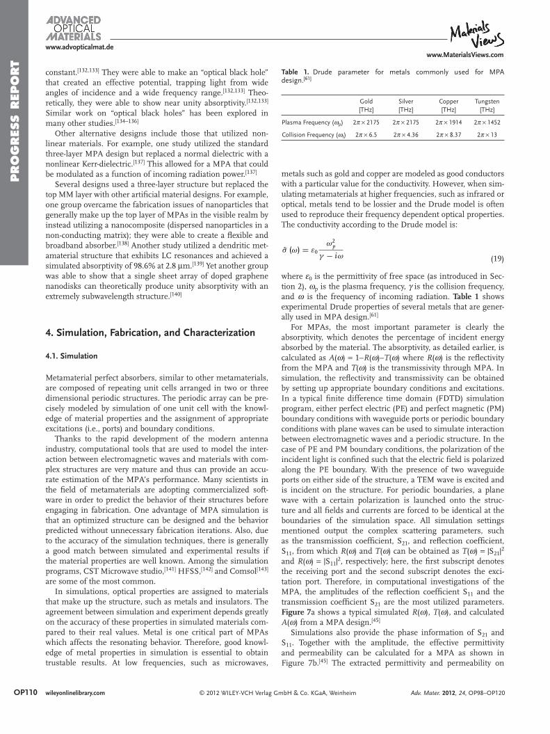
For MPAs, the most important parameter is clearly the absorptivity, which denotes the percentage of incident energy absorbed by the material. The absorptivity, as detailed earlier, is calculated as A ( ω ) = 1– R ( ω )– T ( ω ) where R ( ω ) is the refl ectivity from the MPA and T ( ω ) is the transmissivity through MPA. In simulation, the refl ectivity and transmissivity can be obtained by setting up appropriate boundary conditions and excitations. In a typical fi nite difference time domain (FDTD) simulation program, either perfect electric (PE) and perfect magnetic (PM) boundary conditions with waveguide ports or periodic boundary conditions with plane waves can be used to simulate interaction between electromagnetic waves and a periodic structure. In the case of PE and PM boundary conditions, the polarization of the incident light is confi ned such that the electric fi eld is polarized along the PE boundary. With the presence of two waveguide ports on either side of the structure, a TEM wave is excited and is incident on the structure. For periodic boundaries, a plane wave with a certain polarization is launched onto the struc-ture and all fi elds and currents are forced to be identical at the boundaries of the simulation space. All simulation settings mentioned output the complex scattering parameters, such as the transmission coeffi cient, S 21 , and refl ection coeffi cient, S 11 , from which R ( ω ) and T ( ω ) can be obtained as T ( ω ) = | S 21 | 2 and R ( ω ) = | S 11 | 2 , respectively; here, the fi rst subscript denotes the receiving port and the second subscript denotes the exci-tation port. Therefore, in computational investigations of the MPA, the amplitudes of the refl ection coeffi cient S 11 and the transmission coeffi cient S 21 are the most utilized parameters. Figure 7 a shows a typical simulated R ( ω ), T ( ω ), and calculated A ( ω ) from a MPA design. [ 45 ]
Simulations also provide the phase information of S 21 and S 11 . Together with the amplitude, the effective permittivity and permeability can be calculated for a MPA as shown in Figure 7 b. [ 45 ] The extracted permittivity and permeability on
mbH & Co. KGaA, Weinheim Adv. Mater. 2012, 24, OP98–OP120
PRO
GRES
S R
EPO
RT
www.MaterialsViews.comwww.advopticalmat.de
Figure 7 . (a) Numerical simulations of the electromagnetic response from an infrared MPA. Refl ection (blue line), transmissivity (green line), and absorptivity (red line). (b) Extracted optical constants for the simu-lated design. Figure reproduced with permission. [ 45 ] Copyright 2010, American Physical Society.
Figure 8 . (a) Component of the electric fi eld of the electric resonator ring and cut wire at resonance, and the anti-parallel currents driven by mag-netic coupling. Figure adapted with permission. [ 44 ] Copyright 2008, The Optical Society. (b) Calculated magnetic fi eld intensity lying in-between top resonator and bottom ground plane. Figure adapted with permis-sion. [ 47 ] Copyright 2011, Nature Publishing Group. (c) Energy dissipa-tion distribution in the MPA structure at resonance wavelength. Figure adapted with permission. [ 45 ] Copyright 2010, American Physical Society.
one hand describes the MPA as an effective homogenous mate-rial and, on the other hand, provides the interpretation that explains the underlying mechanism of MPAs.
Some investigations on the detailed properties of MPAs that are not possible in experiments can be realized by simula-tion. For example, the distribution of the electric and magnetic fi elds inside and outside the MPA indicates how the incident electromagnetic fi eld interacts with the structure and may pro-vide information of the primary means of absorption in a MPA. Another parameter of interest is the surface current, which may be used to show the resonating behavior of the metallic por-tions of the MPA. The existence of antiparallel currents on the top and bottom metallic portions further indicate the involve-ment of a magnetic resonance from the MPA. Simulation
© 2012 WILEY-VCH Verlag GmAdv. Mater. 2012, 24, OP98–OP120
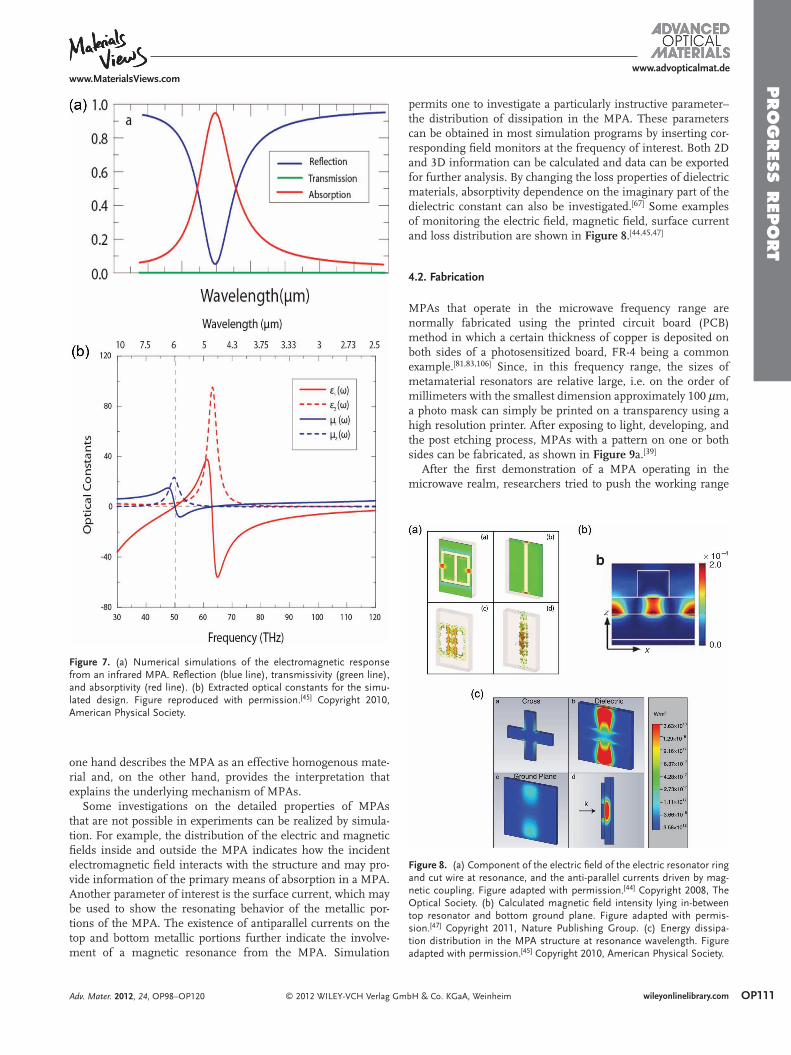
permits one to investigate a particularly instructive parameter–the distribution of dissipation in the MPA. These parameters can be obtained in most simulation programs by inserting cor-responding fi eld monitors at the frequency of interest. Both 2D and 3D information can be calculated and data can be exported for further analysis. By changing the loss properties of dielectric materials, absorptivity dependence on the imaginary part of the dielectric constant can also be investigated. [ 67 ] Some examples of monitoring the electric fi eld, magnetic fi eld, surface current and loss distribution are shown in Figure 8 . [ 44 , 45 , 47 ]
4.2. Fabrication
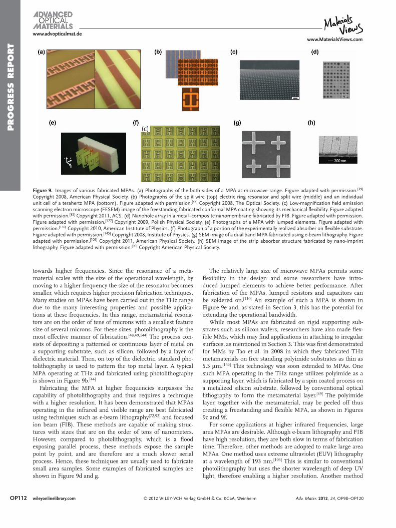
MPAs that operate in the microwave frequency range are normally fabricated using the printed circuit board (PCB) method in which a certain thickness of copper is deposited on both sides of a photosensitized board, FR-4 being a common example. [ 81 , 83 , 106 ] Since, in this frequency range, the sizes of metamaterial resonators are relative large, i.e. on the order of millimeters with the smallest dimension approximately 100 μ m, a photo mask can simply be printed on a transparency using a high resolution printer. After exposing to light, developing, and the post etching process, MPAs with a pattern on one or both sides can be fabricated, as shown in Figure 9 a. [ 39 ]
After the fi rst demonstration of a MPA operating in the microwave realm, researchers tried to push the working range
OP111wileyonlinelibrary.combH & Co. KGaA, Weinheim
OP1
PRO
GRES
S R
EPO
RT
www.MaterialsViews.comwww.advopticalmat.de
Figure 9 . Images of various fabricated MPAs. (a) Photographs of the both sides of a MPA at microwave range. Figure adapted with permission. [ 39 ] Copyright 2008, American Physical Society. (b) Photographs of the split wire (top) electric ring resonator and split wire (middle) and an individual unit cell of a terahertz MPA (bottom). Figure adapted with permission. [ 44 ] Copyright 2008, The Optical Society. (c) Low-magnifi cation fi eld emission scanning electron microscope (FESEM) image of the freestanding fabricated conformal MPA coating showing its mechanical fl exibility. Figure adapted with permission. [ 92 ] Copyright 2011, ACS. (d) Nanohole array in a metal–composite nanomembrane fabricated by FIB. Figure adapted with permission. Figure adapted with permission. [ 177 ] Copyright 2009, Polish Physical Society. (e) Photographs of a MPA with lumped elements. Figure adapted with permission. [ 110 ] Copyright 2010, American Institute of Physics. (f) Photograph of a portion of the experimentally realized absorber on fl exible substrate. Figure adapted with permission. [ 145 ] Copyright 2008, Institute of Physics. (g) SEM image of a dual band MPA fabricated using e-beam lithography. Figure adapted with permission. [ 105 ] Copyright 2011, American Physical Society. (h) SEM image of the strip absorber structure fabricated by nano-imprint lithography. Figure adapted with permission. [ 90 ] Copyright American Physical Society.
towards higher frequencies. Since the resonance of a meta-material scales with the size of the operational wavelength, by moving to a higher frequency the size of the resonator becomes smaller, which requires higher precision fabrication techniques. Many studies on MPAs have been carried out in the THz range due to the many interesting properties and possible applica-tions at these frequencies. In this range, metamaterial resona-tors are on the order of tens of microns with a smallest feature size of several microns. For these sizes, photolithography is the most effective manner of fabrication. [ 48 , 49 , 144 ] The process con-sists of depositing a patterned or continuous layer of metal on a supporting substrate, such as silicon, followed by a layer of dielectric material. Then, on top of the dielectric, standard pho-tolithography is used to pattern the top metal layer. A typical MPA operating at THz and fabricated using photolithography is shown in Figure 9 b. [ 44 ]
Fabricating the MPA at higher frequencies surpasses the capability of photolithography and thus requires a technique with a higher resolution. It has been demonstrated that MPAs operating in the infrared and visible range are best fabricated using techniques such as e-beam lithography [ 72 , 92 ] and focused ion beam (FIB). These methods are capable of making struc-tures with sizes that are on the order of tens of nanometers. However, compared to photolithography, which is a fl ood exposing parallel process, these methods expose the sample point by point, and are therefore are a much slower serial process. Hence, these techniques are usually used to fabricate small area samples. Some examples of fabricated samples are shown in Figure 9 d and g.
12 wileyonlinelibrary.com © 2012 WILEY-VCH Verlag G
The relatively large size of microwave MPAs permits some fl exibility in the design and some researchers have intro-duced lumped elements to achieve better performance. After fabrication of the MPAs, lumped resistors and capacitors can be soldered on. [ 110 ] An example of such a MPA is shown in Figure 9 e and, as stated in Section 3, this has the potential for extending the operational bandwidth.
While most MPAs are fabricated on rigid supporting sub-strates such as silicon wafers, researchers have also made fl ex-ible MMs, which may fi nd applications in attaching to irregular surfaces, as mentioned in Section 3. This was fi rst demonstrated for MMs by Tao et al. in 2008 in which they fabricated THz metamaterials on free standing polyimide substrates as thin as 5.5 μ m. [ 145 ] This technology was soon extended to MPAs. One such MPA operating in the THz range utilizes polyimide as a supporting layer, which is fabricated by a spin coated process on a metalized silicon substrate, followed by conventional optical lithography to form the metamaterial layer. [ 49 ] The polyimide layer, together with the metamaterial, may be peeled off thus creating a freestanding and fl exible MPA, as shown in Figures 9 c and 9 f.
For some applications at higher infrared frequencies, large area MPAs are desirable. Although e-beam lithography and FIB have high resolution, they are both slow in terms of fabrication time. Therefore, other methods are adopted to make large area MPAs. One method uses extreme ultraviolet (EUV) lithography at a wavelength of 193 nm. [ 105 ] This is similar to conventional photolithography but uses the shorter wavelength of deep UV light, therefore enabling a higher resolution. Another method
mbH & Co. KGaA, Weinheim Adv. Mater. 2012, 24, OP98–OP120
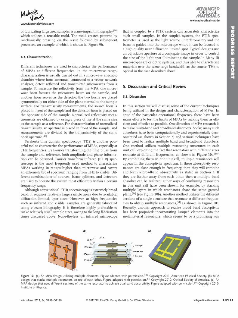
PRO
GRES
S R
EPO
RT
www.advopticalmat.de
www.MaterialsViews.comof fabricating large area samples is nano-imprint lithography, [ 90 ] which utilizes a reusable mold. The mold creates patterns by mechanically pressing on the resist followed by subsequent processes, an example of which is shown in Figure 9 h.
4.3. Characterization
Different techniques are used to characterize the performance of MPAs at different frequencies. In the microwave range, characterization is usually carried out in a microwave anechoic chamber where horn antennas, connected to a vector network analyzer, detect refl ected and transmitted microwaves from a sample. To measure the refl ectivity from the MPA, one micro-wave horn focuses the microwave beam on the sample, and another horn serves as the detector; the two horns are placed symmetrically on either side of the plane normal to the sample surface. For transmissivity measurements, the source horn is placed in front of the sample and the detector horn is placed on the opposite side of the sample. Normalized refl ectivity meas-urements are obtained by using a piece of metal the same size as the sample as a reference. For characterization of normalized transmissivity, an aperture is placed in front of the sample, and measurements are divided by the transmissivity of the same open aperture. [ 48 ]
Terahertz time domain spectroscopy (TDS) is another pow-erful tool to characterize the performance of MPAs, especially at THz frequencies. By Fourier transforming the time pulse from the sample and reference, both amplitude and phase informa-tion can be obtained. Fourier transform infrared (FTIR) spec-troscopy is the most frequently used method to characterize MPAs working in ranges higher than microwave and covers an extremely broad spectrum ranging from THz to visible. Dif-ferent combinations of sources, beam splitters, and detectors are used to operate the system most effi ciently within a certain frequency range.
Although conventional FTIR spectroscopy is extremely broad band, it requires relatively large sample areas due to available, diffraction limited, spot sizes. However, at high frequencies such as infrared and visible, samples are generally fabricated using e-beam lithography. It is therefore highly preferable to make relatively small sample sizes, owing to the long fabrication times discussed above. None-the-less, an infrared microscope
© 2012 WILEY-VCH Verlag Gm
Figure 10 . (a) An MPA design utilizing multiple elements. Figure adapted design that stacks multiple resonators on top of each other. Figure adapteMPA design that uses different sections of the same resonator to achieve dInstitute of Physics.
Adv. Mater. 2012, 24, OP98–OP120
that is coupled to a FTIR system can accurately characterize such small samples. In the coupled system, the FTIR spec-trometer is used as the light source (interferometer) and the beam is guided into the microscope where it can be focused to a high quality near diffraction limited spot. Typical designs use an adjustable aperture at a conjugate image in order to control the size of the light spot illuminating the sample. [ 45 ] Many IR microscopes are catoptric systems, and thus able to characterize materials over the same large bandwidth as the source–THz to optical in the case described above.
5. Discussion and Critical Review
5.1. Discussion
In this section we will discuss some of the current techniques being utilized in the design and characterization of MPAs. In spite of the particular operational frequency, there have been many efforts to test the limits of MPAs by making them as effi -cient and effective as possible. One direction of MPA research is to make multi-band and broadband absorbers. So far, many such absorbers have been computationally and experimentally dem-onstrated (as shown in Section 3) and various techniques have been used to realize multiple band and broadband absorbers. One method utilizes multiple resonating structures in each unit cell, exploiting the fact that resonators with different sizes resonate at different frequencies, as shown in Figure 10 a. [ 105 ] By combining them in one unit cell, multiple resonances will appear in the absorptivity spectrum. If these absorptivity reso-nances are close enough in frequency, then they will combine and form a broadband absorptivity, as stated in Section 3. If they are further away from each other, then a multiple band absorber can be realized. Other ways of combining resonators in one unit cell have been shown; for example, by stacking multiple layers in which resonators share the same ground plane, [ 84 ] (see Figure 10 b). Another method utilizes the different sections of a single structure that resonate at different frequen-cies to obtain multiple resonances, [ 51 ] as shown in Figure 10 c. Recently, another approach to realize broad band absorptivity has been proposed: incorporating lumped elements into the metamaterial resonators, which seems to be a promising way
OP113wileyonlinelibrary.combH & Co. KGaA, Weinheim
with permission. [ 105 ] Copyright 2011, American Physical Society. (b) MPA d with permission. [ 84 ] Copyright 2010, Optical Society of America. (c) An ual band absorptivity. Figure adapted with permission. [ 51 ] Copyright 2010,

OP114
PRO
GRES
S R
EPO
RT
www.MaterialsViews.comwww.advopticalmat.de
of realizing broad band absorbers for microwave frequencies. Although adding lumped elements is a novel and interesting idea, the use of multiple resonating elements in a single unit cell seems to achieve similar results with greater ease of fabri-cation, especially in frequency ranges in which incorporating lumped elements is not feasible, such as THz, IR or optical fre-quencies. There have been studies showing many resonating structures can be integrated into a single unit cell. For example, four, [ 104 ] fi ve, [ 103 ] and remarkably even sixteen [ 105 ] structures have been integrated to achieve a broadband result. Although MPAs have been demonstrated effectively to make multi-band and broadband absorbers, the designs are all based on regular single band MPA. There is little novelty in designing new types of multi-band and broadband absorbers. Additionally, while many researchers are trying to broaden the absorptivity peak of MPAs, there is a lack of efforts to do the opposite, i.e. make an ultra narrow band absorber. For some applications, a delta function like absorptivity is desirable; for example, when using MPAs as single band thermal emitters, as will be discussed in Section 6.
When considering the phenomena of electromagnetic waves incident on MPAs, it is custom to measure only the refl ectivity, transmissivity and calculate absorptivity as A ( ω ) = 1– R ( ω )– T ( ω ). This assumption ignores scattering and other phenomena that may be relevant for accurate characterization. In experiment, any portion of the incident electromagnetic wave that is not gathered by the detector is counted as absorptivity. There is the possibility that the incident energy is scattered or propagates as a SEW without being absorbed, as discussed in Section 2. Although numerical simulation has shown that scattering is not signifi cant at the frequencies where the high absorption is taking place, [ 47 ] experimental demonstration should be carried out to verify the results. Further it is not known if the results in a particular range of the electromagnetic spectrum are general and thus apply to other bands.
5.2. Critical Review
5.2.1. Progress in EM Wave Absorbers
Research in electromagnetic wave absorbers has a long and sto-ried past, as detailed in Section 1. Although the general concept of the Salisbury absorber has been studied for more than 75 years–patented by Salisbury in 1952 [ 5 ] but studied even earlier by Jaumann (sometime during World War II) [ 4 ] and in 1936 by the “Nameless Machinery Company” of the Netherlands, [ 146 , 3 ] –great progress was made with the advent of frequency selective surfaces. By replacing the front lossy material of a Salisbury absorber with a frequency selective surface, these ‘circuit analog’ absorbers permitted multiband and polarization sensitive absorptivity, as well as added an element of tunability. [ 4 ] On the other hand, Dällenbach layer absorbers operate by a different principle; they consist of a homogeneous slab described by ε and μ and backed by a conducting ground plane. The essential idea is to form a layer which has an approximate impedance match with free space by fi nding lossy natural materials which have ε = μ . In this way the refl ectivity of an incident wave will be minimized and absorbed within the material before refl ecting back into free space.
wileyonlinelibrary.com © 2012 WILEY-VCH Verlag G
The geometry of metamaterial absorbers we have described in this Progress Report resembles frequency selective surfaces. However, the main feature of metamaterials is that they permit the construction of composite materials with specifi ed electric, ε , and magnetic, μ , response, where the mechanism of absorp-tion is through impedance matching and loss, i.e. by tailoring the optical constants. They are thus conceptually similar to Däl-lenbach layers. In any case one must question if MMs provide anything new, or if they are simply an extension of the older technology mentioned above.
In order to explore the uniqueness of metamaterials we note that a survey of available literature reveals that, prior to 2008, both Salisbury and Dällenbach absorbers were limited to microwave and lower frequencies. In fact, one prominent fi gure working in the areas of both absorbers and frequency selective surfaces noted in 2003, “Although quite remarkable progress has been demonstrated at the lower frequencies, it is still possible to gain fame and glory by making a contribution at the higher frequencies”, [ 147 ] where “lower” refers to microwave frequencies. In contrast to the limitations of Salisbury and Däl-lenbach layers, plasmonic absorbers were constrained for use at near-infrared and optical wavelengths owing to the natural frequencies of surface plasmon polaritons and localized surface plasmon resonances in metallic structures.
5.2.2. MMs as Novel EM Wave Absorbers
We argue that metamaterials provide a new path forward for the construction of absorbers, as evinced by the great progress made at frequencies at and above the microwave since the fi rst experimentally demonstrated MPA in 2008. In order to clarify the differences and similarities between metamaterials, FSSs and other absorbers, we next highlight some salient features of metamaterials that made this rapid advance possible.
Metamaterials are not limited by and do not depend on the particular properties of the materials they are fashioned from, but rather obtain their exotic properties from their geometry. Designs demonstrated in a particular band of the electromag-netic spectrum may be simply scaled in size to operate in another range; this is possible in spite of the drastic differences in material properties between higher (e.g. optical) and lower (e.g. microwave) frequency bands. Most importantly, metamate-rials are a design concept. That is, metamaterials give one direct access to independently tailor the two parameters that enter into Maxwell’s Equations and which couple material response with electromagnetic waves, ε and μ (inherently volumetric quanti-ties). Metamaterials are thus a bottom-up approach where one pieces together a material through the assembly of ‘artifi cial atoms’, each of which have specifi cally programmed electro-magnetic properties, thus giving rise to materials with emer-gent exotic EM characteristics.
In contrast, frequency selective surfaces are just that: sur-faces. Moreover FSSs permit the tuning of a single parameter, the impedance. These may seem like a minor differences, how-ever, consider the drastic differences in the prescription for designing absorbers. One FSS design method, known as the equivalent circuit method, decomposes individual elements into effective inductive and capacitive constituents of a transmission line. [ 148 , 149 ] Another method, denoted the mutual-impedance
mbH & Co. KGaA, Weinheim Adv. Mater. 2012, 24, OP98–OP120
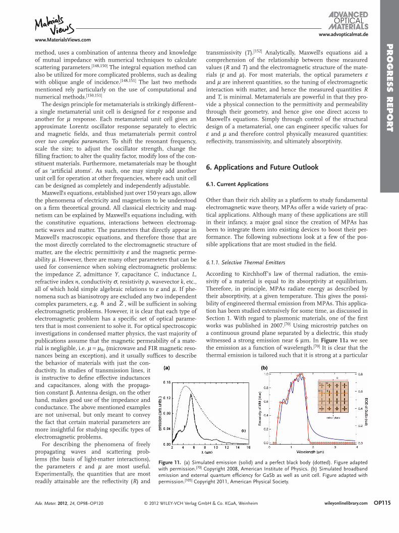
PRO
GRES
S R
EPO
RT
www.MaterialsViews.comwww.advopticalmat.de
method, uses a combination of antenna theory and knowledge of mutual impedance with numerical techniques to calculate scattering parameters. [ 148 , 150 ] The integral equation method can also be utilized for more complicated problems, such as dealing with oblique angle of incidence. [ 148 , 151 ] The last two methods mentioned rely particularly on the use of computational and numerical methods. [ 150 , 151 ]
The design principle for metamaterials is strikingly different–a single metamaterial unit cell is designed for ε response and another for μ response. Each metamaterial unit cell gives an approximate Lorentz oscillator response separately to electric and magnetic fi elds, and thus metamaterials permit control over two complex parameters . To shift the resonant frequency, scale the size; to adjust the oscillator strength, change the fi lling fraction; to alter the quality factor, modify loss of the con-stituent materials. Furthermore, metamaterials may be thought of as ‘artifi cial atoms’. As such, one may simply add another unit cell for operation at other frequencies, where each unit cell can be designed as completely and independently adjustable.
Maxwell’s equations, established just over 150 years ago, allow the phenomena of electricity and magnetism to be understood on a fi rm theoretical ground. All classical electricity and mag-netism can be explained by Maxwell’s equations including, with the constitutive equations, interactions between electromag-netic waves and matter. The parameters that directly appear in Maxwell’s macroscopic equations, and therefore those that are the most directly correlated to the electromagnetic structure of matter, are the electric permittivity ε and the magnetic perme-ability μ . However, there are many other parameters that can be used for convenience when solving electromagnetic problems: the impedance Z , admittance Y , capacitance C , inductance L , refractive index n , conductivity σ , resistivity ρ , wavevector k , etc., all of which hold simple algebraic relations to ε and μ . If phe-nomena such as bianisotropy are excluded any two independent complex parameters, e.g. n and Z , will be suffi cient in solving electromagnetic problems. However, it is clear that each type of electromagnetic problem has a specifi c set of optical parame-ters that is most convenient to solve it. For optical spectroscopic investigations in condensed matter physics, the vast majority of publications assume that the magnetic permeability of a mate-rial is negligible, i.e. μ = μ 0 , (microwave and FIR magnetic reso-nances being an exception), and it usually suffi ces to describe
Figure 11 . (a) Simulated emission (solid) and a perfect black body (dotted). Figure adapted with permission. [ 70 ] Copyright 2008, American Institute of Physics. (b) Simulated broadband emission and external quantum effi ciency for GaSb as well as unit cell. Figure adapted with permission. [ 105 ] Copyright 2011, American Physical Society.
the behavior of materials with just the con-ductivity. In studies of transmission lines, it is instructive to defi ne effective inductances and capacitances, along with the propaga-tion constant β . Antenna design, on the other hand, makes good use of the impedance and conductance. The above mentioned examples are not universal, but only meant to convey the fact that certain material parameters are more insightful for studying specifi c types of electromagnetic problems.
For describing the phenomena of freely propagating waves and scattering prob-lems (the basis of light-matter interactions), the parameters ε and μ are most useful. Experimentally, the quantities that are most readily attainable are the refl ectivity ( R ) and
© 2012 WILEY-VCH Verlag GmAdv. Mater. 2012, 24, OP98–OP120
transmissivity ( T ). [ 152 ] Analytically, Maxwell’s equations aid a comprehension of the relationship between these measured values ( R and T ) and the electromagnetic structure of the mate-rials ( ε and μ ). For most materials, the optical parameters ε and μ are inherent quantities, so the tuning of electromagnetic interaction with matter, and hence the measured quantities R and T, is minimal. Metamaterials are powerful in that they pro-vide a physical connection to the permittivity and permeability through their geometry, and hence give one direct access to Maxwell’s equations. Simply through control of the structural design of a metamaterial, one can engineer specifi c values for ε and μ and therefore control physically measured quantities: refl ectivity, transmissivity, and ultimately absorptivity.
6. Applications and Future Outlook
6.1. Current Applications
Other than their rich ability as a platform to study fundamental electromagnetic wave theory, MPAs offer a wide variety of prac-tical applications. Although many of these applications are still in their infancy, a major goal since the creation of MPAs has been to integrate them into existing devices to boost their per-formance. The following subsections look at a few of the pos-sible applications that are most studied in the fi eld.
6.1.1. Selective Thermal Emitters
According to Kirchhoff’s law of thermal radiation, the emis-sivity of a material is equal to its absorptivity at equilibrium. Therefore, in principle, MPAs radiate energy as described by their absorptivity, at a given temperature. This gives the possi-bility of engineered thermal emission from MPAs. This applica-tion has been studied extensively for some time, as discussed in Section 1. With regard to plasmonic materials, one of the fi rst works was published in 2007. [ 70 ] Using microstrip patches on a continuous ground plane separated by a dielectric, this study witnessed a strong emission near 6 μ m. In Figure 11 a we see the emission as a function of wavelength. [ 70 ] It is clear that the thermal emission is tailored such that it is strong at a particular
OP115wileyonlinelibrary.combH & Co. KGaA, Weinheim
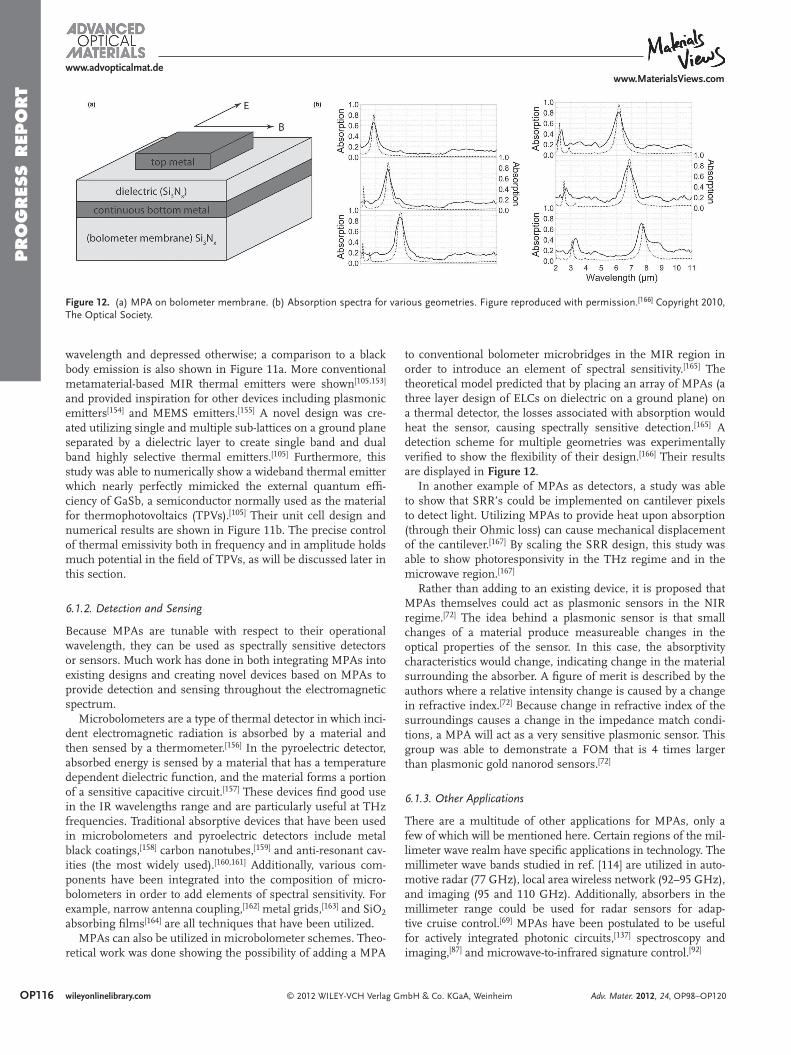
OP116
PRO
GRES
S R
EPO
RT
www.MaterialsViews.comwww.advopticalmat.de
Figure 12 . (a) MPA on bolometer membrane. (b) Absorption spectra for various geometries. Figure reproduced with permission. [ 166 ] Copyright 2010, The Optical Society.
wavelength and depressed otherwise; a comparison to a black body emission is also shown in Figure 11 a. More conventional metamaterial-based MIR thermal emitters were shown [ 105 , 153 ] and provided inspiration for other devices including plasmonic emitters [ 154 ] and MEMS emitters. [ 155 ] A novel design was cre-ated utilizing single and multiple sub-lattices on a ground plane separated by a dielectric layer to create single band and dual band highly selective thermal emitters. [ 105 ] Furthermore, this study was able to numerically show a wideband thermal emitter which nearly perfectly mimicked the external quantum effi -ciency of GaSb, a semiconductor normally used as the material for thermophotovoltaics (TPVs). [ 105 ] Their unit cell design and numerical results are shown in Figure 11 b. The precise control of thermal emissivity both in frequency and in amplitude holds much potential in the fi eld of TPVs, as will be discussed later in this section.
6.1.2. Detection and Sensing
Because MPAs are tunable with respect to their operational wavelength, they can be used as spectrally sensitive detectors or sensors. Much work has done in both integrating MPAs into existing designs and creating novel devices based on MPAs to provide detection and sensing throughout the electromagnetic spectrum.
Microbolometers are a type of thermal detector in which inci-dent electromagnetic radiation is absorbed by a material and then sensed by a thermometer. [ 156 ] In the pyroelectric detector, absorbed energy is sensed by a material that has a temperature dependent dielectric function, and the material forms a portion of a sensitive capacitive circuit. [ 157 ] These devices fi nd good use in the IR wavelengths range and are particularly useful at THz frequencies. Traditional absorptive devices that have been used in microbolometers and pyroelectric detectors include metal black coatings, [ 158 ] carbon nanotubes, [ 159 ] and anti-resonant cav-ities (the most widely used). [ 160 , 161 ] Additionally, various com-ponents have been integrated into the composition of micro-bolometers in order to add elements of spectral sensitivity. For example, narrow antenna coupling, [ 162 ] metal grids, [ 163 ] and SiO 2 absorbing fi lms [ 164 ] are all techniques that have been utilized.
MPAs can also be utilized in microbolometer schemes. Theo-retical work was done showing the possibility of adding a MPA
wileyonlinelibrary.com © 2012 WILEY-VCH Verlag G
to conventional bolometer microbridges in the MIR region in order to introduce an element of spectral sensitivity. [ 165 ] The theoretical model predicted that by placing an array of MPAs (a three layer design of ELCs on dielectric on a ground plane) on a thermal detector, the losses associated with absorption would heat the sensor, causing spectrally sensitive detection. [ 165 ] A detection scheme for multiple geometries was experimentally verifi ed to show the fl exibility of their design. [ 166 ] Their results are displayed in Figure 12 .
In another example of MPAs as detectors, a study was able to show that SRR’s could be implemented on cantilever pixels to detect light. Utilizing MPAs to provide heat upon absorption (through their Ohmic loss) can cause mechanical displacement of the cantilever. [ 167 ] By scaling the SRR design, this study was able to show photoresponsivity in the THz regime and in the microwave region. [ 167 ]
Rather than adding to an existing device, it is proposed that MPAs themselves could act as plasmonic sensors in the NIR regime. [ 72 ] The idea behind a plasmonic sensor is that small changes of a material produce measureable changes in the optical properties of the sensor. In this case, the absorptivity characteristics would change, indicating change in the material surrounding the absorber. A fi gure of merit is described by the authors where a relative intensity change is caused by a change in refractive index. [ 72 ] Because change in refractive index of the surroundings causes a change in the impedance match condi-tions, a MPA will act as a very sensitive plasmonic sensor. This group was able to demonstrate a FOM that is 4 times larger than plasmonic gold nanorod sensors. [ 72 ]
6.1.3. Other Applications
There are a multitude of other applications for MPAs, only a few of which will be mentioned here. Certain regions of the mil-limeter wave realm have specifi c applications in technology. The millimeter wave bands studied in ref. [ 114 ] are utilized in auto-motive radar (77 GHz), local area wireless network (92–95 GHz), and imaging (95 and 110 GHz). Additionally, absorbers in the millimeter range could be used for radar sensors for adap-tive cruise control. [ 69 ] MPAs have been postulated to be useful for actively integrated photonic circuits, [ 137 ] spectroscopy and imaging, [ 87 ] and microwave-to-infrared signature control. [ 92 ]
mbH & Co. KGaA, Weinheim Adv. Mater. 2012, 24, OP98–OP120
PRO
GRES
S R
EPO
RT
www.MaterialsViews.comwww.advopticalmat.de
6.2. Future Outlook
In addition to applications discussed in Section 6.1, there are many great options for future development of MPAs. One is the advent of tunable, or active, metamaterial absorbers, i.e. making a MPA that could be dynamically tuned by means of external stimuli. There has been considerable effort to achieve this not just by the MPA community, but by the metamaterial community as a whole. The fi eld of active metamaterials has made important developments in the past few years with tun-able designs available with MEMS, [ 168 ] liquid crystals, [ 169 ] and the inclusion of elements such as Schottky gates. [ 170 ] There have been a few attempts at a tunable MPA noted in Section 4 (e.g. see references [ 52 , 111 ] ); however, these structures are generally restricted to lower frequencies due to the fact that diodes are included in the construction. Moreover, for higher frequency operation it is highly desirable to achieve monolithic integra-tion of the control components. The future of MPAs will be to create streamlined and effi cient devices that are dynamically tunable.
One particular accessible application of tunable MPAs is in imaging. Some work has been done on THz imaging using compressive sensing. [ 171 ] Compressive sensing utilizes spatial light modulation through various masks and can greatly reduce the number of measurements made with a single pixel detector, which is very benefi cial in the THz regime where it is often time consuming to take multiple measurements. Studies have been done in the past in which metamaterials have been uti-lized as spatial light modulators in the THz regime. [ 172 ] How-ever, there continues to be room for improvement. By utilizing tunable MPAs, one could fashion dynamic pixels that could quickly and easily perform spatial light modulation by utilizing their high absorptivity.
Another possibility, mentioned in the introduction, was the application of MPAs to TPVs. TPVs rely on accurate and effi -cient thermal emission over a specifi c frequency range to maxi-mize effi ciency. Although the effi ciency enhancement of TVPs has been postulated with rare-earth oxides, [ 173 ] plasmonic grat-ings, [ 174 ] and plasmonic nanoparticles, [ 175 ] MPAs offer the pos-sibility of making thermal emitters that are more effi cient and tunable through their designs. [ 105 ] Although much work has been done to understand MPAs as thermal emitters, the future work in this fi eld will involve the inclusion of MPAs into prac-tical TPV devices.
MPAs could also possibly be used for IR camoufl age. It was proposed in 1979 that one could produce camoufl age from IR detection by tailoring the radiation properties to the surrounding environment; this was fi rst proposed for military tanks. [ 176 ] MPAs would make excellent IR camoufl age due to their ability to be selective thermal emitters, as discussed above.
There are a multitude of challenges in the future of MPAs; one is overcoming fabrication issues, specifi cally in the visible realm, to make MPAs as effi cient as possible. Most of these issues as well as proposed solutions have been addressed in Section 4. Another challenge is the inclusion of MPAs into practical devices. Despite the diffi culties and challenges faced by MPAs, we see a bright future with many potential MPA applications which should have a signifi cant impact on current science and technology.
© 2012 WILEY-VCH Verlag GmAdv. Mater. 2012, 24, OP98–OP120
Since their initial development, MPAs have proved to be not only useful for a multitude of applications but also as a plat-form to investigate classical electromagnetic wave theory. As their development over the past three years has been vast and rapid, we are confi dent that their applicability, performance, and ability to span the electromagnetic spectrum will only con-tinue to develop.
Supporting Information Supporting Information is available from the Wiley Online Library or from the author.
Acknowledgements We acknowledge funding from the Offi ce of Naval Research under US Navy Contract Nos. N00014-09-M-0290, N00014-11-1-0583, N00014-11-1-0864 and the Department of Energy under grant number DE-SC0005240.
Received: February 16, 2012Published Online: May 25, 2012
[ 1 ] G. T. Ruck , D. E. Barrick , W. D. Stuart , Radar Cross Section Hand-book , Vol. 2, Plenum , New York 1970 .
[ 2 ] E. Knott , J. F. Shaeffer , M. T. Tuley , Radar Cross Section , 2 nd ed. , Scitech, Raleigh 2004 .
[ 3 ] W. H. Emerson , IEEE Trans. Ant. & Prop. 1973 , AP21 , 484 . [ 4 ] B. A. Munk , Frequency Selective Surfaces , John Wiley & Sons ,
New York 2000 . [ 5 ] W. W. Salisbury , US Patent 1952 2599944 . [ 6 ] B. A. Munk , J. B. Pryor , Proc. Symp. EM Mats. 2003 , 2 , 163 . [ 7 ] E. Popov , D. Maystre , R. C. McPhedran , M. Nevière , M. C. Hutley ,
G.H Derrick , Opt. Exp. 2008 , 16 , 6146 . [ 8 ] R. W. Wood , Phil. Mag. & J. Sci. 1902 , 4 , 396 . [ 9 ] J. Hagglund , F. Sellberg , J. Opt. Soc. Am. 1966 , 56 , 1031 . [ 10 ] D. Maystre , R. Petit , Opt. Comm. 1976 , 17 , 196 . [ 11 ] M. C. Hutley , D. Maystre , Opt. Comm. 1976 , 19 , 431 . [ 12 ] B. Munk , P. Munk , J. Pryor , IEEE Trans. on Ant. and Prop. 2007 , 55 ,
186 . [ 13 ] S. A. Tretyakov , S. I. Maslovski , Mic. and Opt. Tech. Lett. 2003 , 38 ,
175 . [ 14 ] W. Tang , Z. Shen , Elec. Lett. 2007 , 43 , 12 . [ 15 ] A. Namai , S. Sakurai , M. Nakajima , T. Suemoto , K. Matsumoto ,
M. Goto , S. Sasaki , S. Ohkoshi , J. Am. Chem. Soc. 2009 , 131 , 1170 . [ 16 ] G. R. Fowles , Introduction to Modern Optics , 2 nd ed. , Dover Publica-
tions, Mineola, NY , 1989 . [ 17 ] E. A. Vinogradov , G. N. Zhishin , A. G. Mal’shukov , V. I. Yudson ,
Solid State Comm. 1977 , 23 , 915 . [ 18 ] J. J. Greffet , R. Carminati , K. Joulain , J. P. Mulet , S. Mainguy ,
Y. Chen , Nature 2002 , 416 , 61 . [ 19 ] I. Puscasu , M. Pralle , M. McNeal , J. Daly , A. Greenwald , E. Johnson ,
R. Biswas , C. G. Ding , Jo. Appl. Phys. 2005 , 98 , 103531 . [ 20 ] M. U. Pralle , N. Moelders , M. P. McNeal , I. Puscasu ,
A. C. Greenwald , J. T. Daly , E. A. Johnson , T. George , D. S. Choi , E. El-Kady , R. Biswas , Appl. Phys. Lett. 2002 , 81 , 4685 .
[ 21 ] M. W. Tsai , T. H. Chuang , C. Y. Meng , Y. T. Chang , S. C. Lee , Appl. Phys. Lett. 2006 , 89 , 173116 .
OP117wileyonlinelibrary.combH & Co. KGaA, Weinheim
OP118
PRO
GRES
S R
EPO
RT
www.MaterialsViews.comwww.advopticalmat.de
[ 22 ] C. M Wang , Y. C. Chang , M. W. Tsai , Y. H. Ye , C.Y Chen , Y. W. Jiang , Y. T. Chang , S. C. Lee , D. P. Tsai , Opt. Exp. 2007 , 15 , 14673 .
[ 23 ] J. B. Pendry , A. J. Holden , W. J. Stewart , I. Youngs , Phys. Rev. Lett. 1996 , 76 , 4773 .
[ 24 ] J. B. Pendry , A. J. Holden , D. J. Robbins , W. J. Stewart , IEEE Trans. Microwave Theory Tech. 1999 , 47 , 2075 .
[ 25 ] V. G. Veselago , Sov. Phys. Usp. 1968 , 10 , 509 . [ 26 ] D. R. Smith , W. J. Padilla , D. C. Vier , S. C. Nemat-Nasser ,
S. Schultz , Phys. Rev. Lett. 2000 , 84 , 4184 . [ 27 ] R. A. Shelby , D. R. Smith , S. Schultz , Science 2001 , 292 , 77 . [ 28 ] W. J. Padilla , D. R. Smith , D. N. Basov , J. Opt. Soc. Am. B 2006 , 23 ,
404 . [ 29 ] S. Linden , C. Enkrich , M. Wegener , J. Zhou , T. Koschny ,
C. M. Soukoulis , Science 2004 , 306 , 1351 . [ 30 ] S. Zhang , W. Fan , B. K. Minhas , A. Frauenglass , K. J. Malloy ,
S. R. J. Brueck , Phys. Rev. Lett. 2005 , 94 , 037402 . [ 31 ] T. J. Yen , W. J. Padilla , N. Fang , D. C. Vier , D. R. Smith , J. B. Pendry ,
D. N. Basov , X. Zhang , Science 2004 , 303 , 1494 . [ 32 ] M. Bayindir , K. Aydin , E. Ozbay , P Markos , C. M. Soukoulis , Appl.
Phys. Lett. 2002 , 81 , 120 . [ 33 ] C. M. Soukoulis , S. Linden , M. Wgener , Science 2007 , 315 , 47 . [ 34 ] D. Schurig , J. J. Mock , B. J. Justice , S. A. Cummer , J. B. Pendry ,
A. F. Starr , D. R. Smith , Science 2006 , 314 , 977 . [ 35 ] J. B. Pendry , Phys. Rev. Lett. 2000 , 85 , 3699 . [ 36 ] N. Fang , H. Lee , C. Sun , X. Zhang , Science 2005 , 308 , 534 . [ 37 ] Z. Liu , H. Lee , Y. Xiong , C. Sun , X. Zhang , Science 2007 , 315 , 1686 . [ 38 ] D. Schurig , D. R. Smith , Phys. Rev. E 2004 , 70 , 065601(R) . [ 39 ] N. I. Landy , S. Sajuyigbe , J. J. Mock , D. R. Smith , W. J. Padilla , Phys.
Rev. Lett. 2008 , 100 , 207402 . [ 40 ] R. Marques , F. Medina , R. Rafi i-El-Idrissi , Phys. Rev. B 2002 , 65 ,
144440 . [ 41 ] W. J. Padilla , Optics Express 2007 , 15 , 1639 . [ 42 ] D. R. Smith , Phys. Rev. E 2010 , 81 , 036605 . [ 43 ] N. Engheta , IEEE Ant. & Prop. Soc. Int. Symp. 2002 , 92 , 2 . [ 44 ] H. Tao , N. I. Landy , C. M. Bingham , X. Zhang , R. D. Averitt ,
W. J. Padilla , Opt. Exp. 2008 , 16 , 7181 . [ 45 ] X. Liu , T. Starr , A. F. Starr , W. J. Padilla , Phys. Rev. Lett. 2010 , 104 ,
207403 . [ 46 ] Y. Avitzour , Y. A. Urzhumov , G. Shvets , Phys. Rev. B. 2008 , 79 ,
045131 . [ 47 ] K. Aydin , V. E. Ferry , R. M. Briggs , H. A. Atwater , Nat. Comm. 2011 ,
2 , 517 . [ 48 ] N. I. Landy , C. M. Bingham , T. Tyler , N. Jokerst , D. R. Smith ,
W. J. Padilla , Phys. Rev. B 2009 , 79 , 125104 . [ 49 ] H. Tao , C. M. Bingham , A. C. Strikwerda , D. Pilon , D. Shrekenhamer ,
N. I. Landy , K. Fan , X. Zhang , W. J. Padilla , R. D. Averitt , Phys. Rev. B 2008 , 78 , 241103 .
[ 50 ] Q. Y. Wen , H. W. Zhang , Y. S. Xie , Q. H. Yang , Y. L. Liu , Appl. Phys. Lett. 2009 , 95 , 241111 .
[ 51 ] H. Tao , C. M. Bingham , D. Pilon , K. Fan , A. C. Strikwerda , D. Shrekenhamer , W. J. Padilla , X. Zhang , R. D.Averitt , J. Phys. D 2010 , 43 , 225102 .
[ 52 ] B. Zhu , C. Huang , Y. Feng , J. Zhao , T. Jiang , PIER B 2010 , 24 , 121 . [ 53 ] R. H. Ritchie , Phys. Rev. 1957 , 106 , 874 . [ 54 ] A. Sommerfeld , Annalen der Physik und Chemie 1899 , 67 , 233 . [ 55 ] F. Harms , Annal. Phys. 1907 , 23 , 44 . [ 56 ] J. Zenneck , Annal. Phys. 1907 , 23 , 846 . [ 57 ] G. Goubau , J. Appl. Phys. 1950 , 21 , 1119 . [ 58 ] A. F. Harvey , IEEE Trans. Microw. Theory and Tech. 1960 , 8 , 30 . [ 59 ] H. Raether , Surface Plasmons on Smooth and Rough Surfaces and on
Gratings , Springer Tracts in Modern Physics 111, Springer-Verlag, New York 1988 .
[ 60 ] P. Markos , Costas M. Soukoulis , Wave Propagation: From Electrons to Photonic Crystals and Left-Handed Materials , Princeton University Press , New Jersey 2008 .
wileyonlinelibrary.com © 2012 WILEY-VCH Verlag G
[ 61 ] M. A. Ordal , L. L. Long , R. J. Bell , S. E. Bell , R. R. Bell , R. W. Alexander , Jr. , C. A. Ward , Appl. Opt. 1983 , 22 , 1099 .
[ 62 ] J. A. Kong , Electromagnetic Wave Theory , 2 nd Ed. , John Wiley & Sons, Inc ., New York 1990 .
[ 63 ] R. de L. Kronig , J. Opt. Soc. Am. 1926 , 12 , 547 . [ 64 ] H. A. Kramers , Atti Cong. Intern. Fisica (Transactions of Volta Cente-
nary Congress) , Como 1927 , 2 , 545 . [ 65 ] R. M. Fano , J. Franklin Inst. 1950 , 249 , 139 . [ 66 ] K. N. Rozanov , IEEE Trans. Antennas Propag. 2000 , 48 , 1230 . [ 67 ] C. G. Hu , X. Li , Q. Feng , X. N. Chen , X. G. Luo , Opt. Exp. 2010 , 18 ,
6598 . [ 68 ] C. M. Bingham , H. Tao , X. Liu , R. D. Averitt , X. Zhang , W. J. Padilla ,
Opt. Exp. 2008 , 16 , 18565 . [ 69 ] A. I. M. Ayala , Master of Science Thesis, Tufts University, USA,
2009 . [ 70 ] I. Puscasu , W. L. Schaich , Appl. Phys. Lett. 2008 , 92 , 233102 . [ 71 ] J. Hao , J. Wang , X. Liu , W. J. Padilla , L. Zhou , M. Qiu , Appl. Phys.
Lett. 2010 , 96 , 251104 . [ 72 ] N. Liu , M. Mesch , T. Weiss , M. Hentschel , H. Giessen , Nano Lett.
2010 , 10 , 2342 . [ 73 ] J. Wang , Y. Chen , X. Chen , J. Hao , M. Yan , M. Qiu , Opt. Exp. 2011 ,
19 , 14726 . [ 74 ] S. O’Brien , D. McPeake , S. A. Ramakrishna , J. B. Pendry , Phys. Rev.
B 2004 , 69 , 241101(R) . [ 75 ] R. Marqués , F. Medina , R. Rafi i-El-Idrissi , Phys. Rev. B 2002 , 65 ,
144440 . [ 76 ] D. R. Smith , J. Gollub , J. J. Mock , W. J. Padilla , D. Schurig , J. Appl.
Phys. 2006 , 100 , 024507 . [ 77 ] D. R. Smith , D. Schurig , J. J. Mock , Phys. Rev. E 2006 , 74 ,
036604 . [ 78 ] D. Schurig , J. J. Mock , D. R. Smith , Appl. Phys. Lett. 2005 , 88 ,
041109 . [ 79 ] W. J. Padilla , M. T. Aronsson , C. Highstrete , M. Lee , A. J. Taylor ,
R. D. Averitt , Physical Review B Rapids 2007 , 75 , 041102(R) . [ 80 ] G. Chao , Q. S. Bo , P. Z. Bin , Chin. Phys. B 2011 , 20 ,
037801 . [ 81 ] B. Zhu , Z. B. Wang , Z. Z. Yu , Q. Zhang , J. M. Zhao , Y. J. Feng ,
T. Jiang , Chin. Phys. Lett. 2009 , 26 , 114102 . [ 82 ] Y. Q. Xu , P. H. Zhou , H. B. Zhang , L. Chen , L. J. Deng , Jo. Appl.
Phys. 2011 , 110 , 044102 . [ 83 ] B. Wang , T. Koschny , C. M. Soukoulis , Phys. Rev. B 2009 , 80 ,
033108 . [ 84 ] Y. Q. Ye , Y. Jin , S. He , J. Opt. Soc. Am. 2010 , 27 , 498 . [ 85 ] C. Gu , S. Qu , Z. Pei , H. Zhou , J. Wang , PIER Lett. 2010 , 17 , 171 . [ 86 ] Y. Ma , Q. Chen , J. Grant , S. C. Saha , A. Khalid , D. R. S. Cumming ,
Opt. Lett. 2011 , 36 , 945 . [ 87 ] X. J. He , Y. Wang , J. M. Wang , T. L. Gui , PIER 2011 , 115 , 381 . [ 88 ] L. Huang , D. R. Chowdhury , S. Ramani , M. T. Reiten , S. N. Luo ,
A. J. Taylor , H. T. Chen , Opt. Lett. 2012 , 37 , 154 . [ 89 ] D. Y. Shchegolkov , A. K. Azad , J. F. O’Hara , E. I. Simakov , Phys.
Rev. B 2010 , 82 , 205117 . [ 90 ] C. Wu , B. Neuner III , G. Shvets , J. John , A. Milder , B. Zollars ,
S. Savoy , Phys. Rev. B. 2011 , 84 , 075102 . [ 91 ] J. Wang , Y. Chen , J. Hao , M. Yan , M. Qiu , J. Appl. Phys. 2011 , 109 ,
074510 . [ 92 ] Z. H. Jiang , S. Yun , F. Toor , D. H.Werner , T. S. Mayer , ACS Nano
2011 , 5 , 4641 . [ 93 ] K. B. Alici , A. B. Turhan , C. M. Soukoulis , E. Ozbay , Opt. Exp. 2011 ,
19 , 14260 . [ 94 ] W. Zhu , X. Zhao , B. Gong , L. Liu , B. Su , Appl. Phys. A 2011 , 102 ,
147 . [ 95 ] F. Bilotti , A. Toscano , K. B. Alici , E. Ozbay , L. Vegni , IEEE Trans. on
EM Comp. 2011 , 53 , 63 . [ 96 ] M. Diem , T. Koschny , C. M. Soukoulis , Phys. Rev. B 2009 , 79 ,
033101 .
mbH & Co. KGaA, Weinheim Adv. Mater. 2012, 24, OP98–OP120
PRO
GRES
S R
EPO
RT
www.MaterialsViews.comwww.advopticalmat.de
[ 97 ] W. J. Padilla , International Workshop on Meta-materials and Plas-monics, Fudan University, Shanghai, China , November 13–15, 2008 .
[ 98 ] Q. Y. Wen , Y. Xie , H. Zhang , Q. Yang , B. Liu , Chin. J. Opt. & Appl. Opt. 2010 , 3 , 70 .
[ 99 ] G. Chao , Q. S. Bo , P. S. Bin , Chin. Phys. B 2011 , 20 , 017801 . [ 100 ] M. H. Li , H. L. Yang , X. W. Hou , Y. Tian , D. Y. Hou , PIER 2010 , 108 ,
37 . [ 101 ] H. Li , L. H. Yuan , B. Zhou , X. P. Shen , Q. Cheng , J. Appl. Phys.
2011 , 110 , 014909 . [ 102 ] X. Shen , T. J. Cui , J. Zhao , H. F. Ma , W. X. Jiang , H. Li , Opt. Exp.
2011 , 19 , 9401 . [ 103 ] H. Luo , T. Wang , R. Z. Gong , Y. Nie , X. Wang , Chin. Phys. Lett.
2011 , 28 , 034204 . [ 104 ] H. Luo , Y. Z. Cheng , R. Z. Gong , Eur. Phys. Jo. B 2011 , 81 , 387 . [ 105 ] X. Liu , T. Tyler , T. Starr , A. Starr , N. M. Jokerst , W. J. Padilla , Phys.
Rev. Lett. 2011 , 107 , 045901 . [ 106 ] L. Huang , H. Chen , PIER 2011 , 113 , 103 . [ 107 ] M. Lockyear , A. P Hibbins , J. R. Sambles , P. A. Hobson ,
C. R. Lawrence , Appl. Phys. Lett. 2009 , 94 , 041913 . [ 108 ] L. Li , Y. Yang , C. Liang , Jo. Appl. Phys. 2011 , 110 , 063702 . [ 109 ] G. Chao , S. B. Qu , Z. B. Pei , H. Zhou , X. Zhiy , B. Peng , P. Dong ,
L. Qin , Chin. Phys. Lett. 2010 , 27 , 117802 [ 110 ] S. Gu , J. P. Barrett , T. H. Hand , B.-I. Popa , S. A. Cummer , J. Appl.
Phys. 2010 , 108 , 064913 . [ 111 ] B. Zhu , J. Zhao , C. Huang , T. Jiang , Appl. Phys. Lett. 2010 , 97 ,
051906 . [ 112 ] K. B. Alici , F. Bilotti , L. Vegni , E. Ozbay , Jo. Appl. Phys. 2010 , 108 ,
083113 . [ 113 ] Y. Cheng , H. Yang , Z. Cheng , N. Wu , Appl. Phys. A 2011 , 102 , 99 . [ 114 ] P. Singh , K. A. Korolev , M. N. Afsar , S. Sonkusale , Appl. Phys. Lett.
2011 , 99 , 264101 . [ 115 ] J. Wang , S. Qu , Z. Xu , H. Ma , Y. Yang , C. Gu , X. Wu , Jo. Magn. &
Mag. Mat. 2009 , 321 , 2805 . [ 116 ] J. F. Wang , S. B. Qu , Z. T. Fu , H. Ma , Y. M. Yang , X. Wu , PIER Lett.
2009 , 17 , 15 . [ 117 ] P. Ding , E. Liang , G. Cai , W. Hu , C. Fan , Q. Xue , Jour. Opt. 2011 ,
13 , 075005 . [ 118 ] J. Hao , L. Zhou , M. Qiu , Phys. Rev. B 2011 , 83 , 165107 . [ 119 ] M. Wang , C. Hu , M. Pu , C. Huang , Z. Zhao , Q. Reng , X. Luo , Opt.
Exp. 2011 , 19 , 20642 . [ 120 ] L. Xia , H. Gao , H. Shi , Comp. & Theo. Nano. Sci. 2011 , 8 , 27 . [ 121 ] T. W. Ebbesen , H. J. Lazec , H. F. Ghaemi , T. Thio , P. A. Wolff ,
Nature 1998 , 391 , 667 . [ 122 ] I. S. Spevak , A. Y. Nikitin , E. V. Bezuglyi , A. Levchenko , A. V. Kats ,
Phys. Rev. B 2009 , 79 , 161406 . [ 123 ] J. Braun , B. Gompf , G. Kobiela , M. Dressel , Phys. Rev. Lett. 2009 ,
103 , 203901 . [ 124 ] C. Hu , Z. Zhao , X. Chen , X. Luo , Opt. Exp. 2009 , 17 , 11039 . [ 125 ] C. Hu , L. Liu , Z. Zhao , X. Chen , X. Luo , Opt. Exp. 2009 , 17 , 16745 . [ 126 ] F. Yu , H. Wang , S. Zou , J. Phys. Chem. C 2010 , 114 , 2066 . [ 127 ] Y. Gou , Y. Xuan , Y. Han , Int. J. ThermoPhys. 2011 , 32 , 1060 . [ 128 ] R. L. Chern , Y. T. Chen , H. Y. Lin , Opt. Exp. 2010 , 19 , 19510 . [ 129 ] C. H. Lin , R. L. Chern , H. Y. Lin , Opt. Exp. 2011 , 19 , 415 . [ 130 ] R. L. Chern , W. T. Hong , Opt. Exp. 2011 , 19 , 8962 . [ 131 ] A. Tittl , P. Mai , R. Taubert , D. Dregely , N. Liu , H. Giessen , Nano
Lett. 2011 , 11 , 4366 . [ 132 ] E. E. Narimanov , A. V. Kildeshev , Appl. Phys. Lett. 2009 , 95 ,
041106 . [ 133 ] A. Kildishev , L. J. Prokopeva , E. Narimanov , Opt. Exp. 2010 , 18 ,
16646 . [ 134 ] C. Argyropoulos , E. Kallos , Y. Zhan , H. Yang Opt. Exp. 2009 , 17 ,
10 . [ 135 ] J. Ng , H. Chen , C. T. Chan , Opt. Lett. 2009 , 34 , 644 .
© 2012 WILEY-VCH Verlag GAdv. Mater. 2012, 24, OP98–OP120
[ 136 ] C. Argyropoulos , E. Kallos , Y. Hao , J. Opt. Soc. Am. B 2010 , 27 , 2020 .
[ 137 ] Y. Gong , Z. Li , J. Fu , Y. Chen , G. Wang , H. Lu , L. Wang , X. Liu , Opt. Exp. 2011 , 19 , 10193 .
[ 138 ] M. K. Hedayati , M. Javaherirahim , B. Mozooni , R. Abdelaziz , A. Tavassolizadeh , V. S. K. Chakravadhanula , V. Zaporojtchenko , T. Strunkus , F. Faupel , M. Elbahri , Adv. Mat. 2011 , 23 , 5410 .
[ 139 ] W. Zhu , X. Zhao , J. Opt. Soc. Am. 2009 , 26 , 2382 . [ 140 ] S. Thongrattanasiri , F. H. L. Koppens , F. J. Garcia de Abajo , Phys.
Rev. Lett. 2012 , 108 , 047401 . [ 141 ] CST Computer Simulation Technology: www.cst.com/, accessed
date: January 2012. [ 142 ] ANSYS HFSS: www.ansoft.com/products/hf/hfss/, accessed date:
January 2012. [ 143 ] Comsol Multiphysics: www.comsol.com/, accessed date: January
2012. [ 144 ] Y. Cheng , H. Yang , J. Appl. Phys. 2010 , 108 , 034906 . [ 145 ] H. Tao , A. C. Strikwerda , K. Fan , C. M. Bingham , W. J. Padilla ,
X. Zhang , R. D. Averitt , J. Phys. D 2008 , 41 , 232004 . [ 146 ] Naamlooze Vennootschap Machmerieen, French Patent 802 728,
Feb. 19, 1936 . [ 147 ] B. A. Munk , J. B. Pryor , Y. B. Gan , in Electromagnetic Materials:
Proceedings of the Symposium F , ICMAT (Eds: L. Hock, O. C. Kim, S. Matitsine, G. Y. Beng), World Scientifi c Publishing Co. Pte. Ltd. , Singapore 2003 .
[ 148 ] T. K. Wu , Frequency Selective Surfaces and Grid Arrays , John Wiley and Sons , New York 1995 .
[ 149 ] I. Anderson , Bell.Syst. Tech. J. 1975 , 54 , 1725 . [ 150 ] B. A. Munk , E. Pelton , IEEE Trans. on Ant. Prop. 1979 , AP-27 , 323 . [ 151 ] C. C. Chen , IEEE Trans. on Mic. Theory. and Tech. 1973 , MTT-21 , 1 . [ 152 ] F. Wooten , Optical Properties of Solids , Academic Press , New York
1972 . [ 153 ] W. J. Padilla , Int. Conf. on IR, MM, and THz Waves 2009 , Busan,
South Korea . [ 154 ] Y. C. Chang , C. M. Wang , M. N. Abbas , M. H. Shih , D. P. Tsai , Opt.
Exp. 2009 , 17 , 13526 . [ 155 ] J. J. Lai , H. F. Liang , Z. L. Peng , X. Yi , X. F. Zhai , 3 rd Int. Photonics &
OptoElectronics Meet. 2011 , 276 , 012129 . [ 156 ] R. A. Wood , in Infrared Detectors and Emitters: Materials and Devices
(Eds: P. Capper, C. T. Elliot), Kluwer Academic Publishers , Norwell, USA 2001 .
[ 157 ] R. W. Whatmore , R. Watton , in Infrared Detectors and Emitters: Materials and Devices (Eds: P. Capper, C. T. Elliot), Kluwer Aca-demic Publishers , Norwell, USA 2001 .
[ 158 ] J. Lehman , E. Theocharous , G. Eppeldauer , C. Pannel , Meas. Sci. and Tech. 2003 , 14 , 916 .
[ 159 ] J. Lehman , C. Engtrakul , T. Gennett , A. C. Dillon , Appl. Opt. 2005 , 44 , 483 .
[ 160 ] B. E. Cole , US Patent 1994 5286976 . [ 161 ] G. D. Skidmore , C. G. Howard , US Patent 2009 7622717 . [ 162 ] M. A. Gritz , M. Metzler , D. Malocha , M. Abel-Rahman , B. Monacelli ,
G. Zummo , G. D. Boreman , J. Vac. Sci. and Tech. 2004 , 22 , 3133 . [ 163 ] S. W. Han , J. W. Kim , Y. S. Sohn , D. P. Neikirk , Elect. Lett. 2004 , 40 ,
1410 . [ 164 ] A. S. Garwarikar , R. P. Shea , A. Mehdaoui , J. J. Talghader , Inter-
national Conference on Optical MEMS and Nanophotonics 2008 , 178 .
[ 165 ] T. Maier , H. Brückl , Opt. Lett. 2009 , 34 , 3012 . [ 166 ] T. Maier , H. Brückl , Opt. Lett. 2010 , 35 , 3766 . [ 167 ] H. Tao , E. A. Kadlec , A. C. Strikwerda , K. Fan , W. J. Padilla ,
R. D.Averitt , E. A. Shaner , X. Zhang , Opt. Exp. 2011 , 19 , 21620 .
[ 168 ] T. Hand , S. Cummer , IEEE Ant. & Wireless Prop. Lett. 2007 , 6 , 401.
OP119wileyonlinelibrary.commbH & Co. KGaA, Weinheim

OP120
PRO
GRES
S R
EPO
RT
www.MaterialsViews.comwww.advopticalmat.de
[ 169 ] Q. Zhao , L. Kang , B. Du , B. Li , J. Zhou , H.Tang , X. Liang , B. Zhang , Appl. Phys. Lett. 2007 , 90 , 011112 .
[ 170 ] H. T. Chen , W. J. Padilla , J. M. O. Zide , A. C. Gossard , A. J. Taylor , R. D. Averitt , Nature 2006 , 444 , 597 .
[ 171 ] W. L. Chan , K. Charan , D. Takhar , K. F. Kelly , R. G. Baraniuk , D. M. Mittleman , Appl. Phys. Lett. 2008 , 93 , 121102 .
[ 172 ] W. L. Chan , H. T. Chen , A. J. Taylor , I. Brenner , M. J. Cich , D. M. Mittleman , Appl. Phys. Lett. 2009 , 94 , 213511 .
wileyonlinelibrary.com © 2012 WILEY-VCH Verlag G
[ 173 ] G. Torsello , M. Lomascolo , A. Licciulli , D. Diso , S. Tundo & M. Mazzer , Nat. Mater. 2004 , 3 , 632 .
[ 174 ] N. Panotu , C Osgood , M Richard , Opt. Lett. 2007 , 32 , 2825 .
[ 175 ] J. R. Cole , N. J. Halas , Appl. Phys. Lett. 2006 , 89 , 153120 . [ 176 ] E. F. Bienz , US Patent 1979 4, 142, 015 . [ 177 ] Z. Jakšica , D. Tanaskovica , J. Matovicb , Acta Physica Polonica A.
2009 , 116 , 625.
mbH & Co. KGaA, Weinheim Adv. Mater. 2012, 24, OP98–OP120