Embed Size (px)
Citation preview
Terahertz Science and Technology, ISSN 1941-7411 Vol. 6, No. 1, March 2013
40
Invited Paper
Terahertz metamaterial absorbers Mohammad Parvinnezhad Hokmabadi, David S. Wilbert, Patrick Kung , Seongsin M. Kim *
Electrical and Computer Engineering Department, University of Alabama, USA
* Email: [email protected]
(Received January 2, 2013)
Abstract: Terahertz (THz) electromagnetic waves share a few of the characteristics of optical and gigahertz waves, which makes them suitable for a number of interesting and new applications in imaging, spectroscopy, characterization, sensing and monitoring. Recently, there has been a huge interest in developing THz devices that can achieve this potential. One of these devices is a metamaterial THz perfect absorber, which was first proposed in 2008 and is believed to form the basis for future room temperature THz detectors. Since then, a large amount of research has been focused on developing such THz absorbers with various properties, including dual band, multiband, wide band and polarization insensitivity. In this article, we present a brief review of the current state-of-the-art of THz metamaterial absorbers and discuss in more detail two specific THz absorber structures.
Keywords: Terahertz, Metamaterial, Absorber
doi: 10.11906/TST.040-058.2013.03.03
1. Introduction
Terahertz (THz) electromagnetic (EM) waves, with a frequency ranging from 0.1 THz up to 10 THz, share a common properties with optical and gigahertz EM waves. In the infrared, optical and ultraviolet spectral range, the photon is the principal particle and fundamental concept that governs interactions between materials and EM waves, whereas at gigahertz frequencies major electron oscillations in the material are best amenable to describe material-EM wave interactions. Like micro- and millimeter waves, THz radiation can penetrate through a wide variety of non-conducting materials such as fabric, paper, plastic and wood. THz radiation is also non-ionizing and can be absorbed by molecules such as water and DNA. Moreover, since biological molecules exhibit a number of intermolecular and intramolecular modes with resonance frequencies in the THz regime, THz waves are expected to be able to interact with and reveal them with a certain degree of specificity [1]. These characteristics of THz waves make them suitable for a growing number of potential applications in biomedical imaging [2], environmental monitoring of earth [3], remote sensing of explosives [4], and semiconductor spectroscopic characterization [5, 6].
A conventional microwave absorber, called Salisbury screen, was invented in 1952 and consisted of a resistive sheet and a metallic back plane separated by a dielectric spacer [7]. Its operational principle was based on achieving impedance matching with free space through
Terahertz Science and Technology, ISSN 1941-7411 Vol. 6, No. 1, March 2013
41
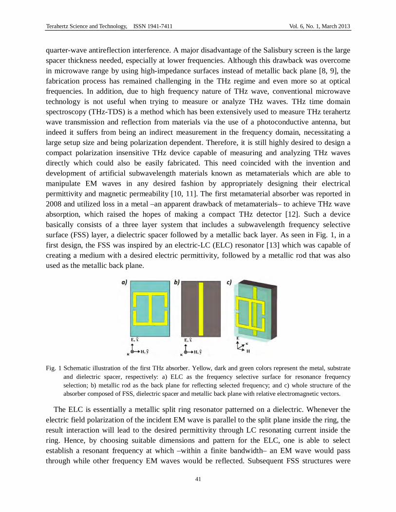
quarter-wave antireflection interference. A major disadvantage of the Salisbury screen is the large spacer thickness needed, especially at lower frequencies. Although this drawback was overcome in microwave range by using high-impedance surfaces instead of metallic back plane [8, 9], the fabrication process has remained challenging in the THz regime and even more so at optical frequencies. In addition, due to high frequency nature of THz wave, conventional microwave technology is not useful when trying to measure or analyze THz waves. THz time domain spectroscopy (THz-TDS) is a method which has been extensively used to measure THz terahertz wave transmission and reflection from materials via the use of a photoconductive antenna, but indeed it suffers from being an indirect measurement in the frequency domain, necessitating a large setup size and being polarization dependent. Therefore, it is still highly desired to design a compact polarization insensitive THz device capable of measuring and analyzing THz waves directly which could also be easily fabricated. This need coincided with the invention and development of artificial subwavelength materials known as metamaterials which are able to manipulate EM waves in any desired fashion by appropriately designing their electrical permittivity and magnetic permeability [10, 11]. The first metamaterial absorber was reported in 2008 and utilized loss in a metal –an apparent drawback of metamaterials– to achieve THz wave absorption, which raised the hopes of making a compact THz detector [12]. Such a device basically consists of a three layer system that includes a subwavelength frequency selective surface (FSS) layer, a dielectric spacer followed by a metallic back layer. As seen in Fig. 1, in a first design, the FSS was inspired by an electric-LC (ELC) resonator [13] which was capable of creating a medium with a desired electric permittivity, followed by a metallic rod that was also used as the metallic back plane.
Fig. 1 Schematic illustration of the first THz absorber. Yellow, dark and green colors represent the metal, substrate and dielectric spacer, respectively: a) ELC as the frequency selective surface for resonance frequency selection; b) metallic rod as the back plane for reflecting selected frequency; and c) whole structure of the absorber composed of FSS, dielectric spacer and metallic back plane with relative electromagnetic vectors.
The ELC is essentially a metallic split ring resonator patterned on a dielectric. Whenever the electric field polarization of the incident EM wave is parallel to the split plane inside the ring, the result interaction will lead to the desired permittivity through LC resonating current inside the ring. Hence, by choosing suitable dimensions and pattern for the ELC, one is able to select establish a resonant frequency at which –within a finite bandwidth– an EM wave would pass through while other frequency EM waves would be reflected. Subsequent FSS structures were
Terahertz Science and Technology, ISSN 1941-7411 Vol. 6, No. 1, March 2013
42
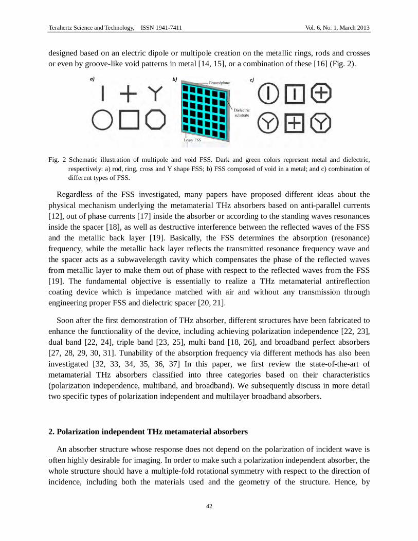
designed based on an electric dipole or multipole creation on the metallic rings, rods and crosses or even by groove-like void patterns in metal [14, 15], or a combination of these [16] (Fig. 2).
Fig. 2 Schematic illustration of multipole and void FSS. Dark and green colors represent metal and dielectric, respectively: a) rod, ring, cross and Y shape FSS; b) FSS composed of void in a metal; and c) combination of different types of FSS.
Regardless of the FSS investigated, many papers have proposed different ideas about the physical mechanism underlying the metamaterial THz absorbers based on anti-parallel currents [12], out of phase currents [17] inside the absorber or according to the standing waves resonances inside the spacer [18], as well as destructive interference between the reflected waves of the FSS and the metallic back layer [19]. Basically, the FSS determines the absorption (resonance) frequency, while the metallic back layer reflects the transmitted resonance frequency wave and the spacer acts as a subwavelength cavity which compensates the phase of the reflected waves from metallic layer to make them out of phase with respect to the reflected waves from the FSS [19]. The fundamental objective is essentially to realize a THz metamaterial antireflection coating device which is impedance matched with air and without any transmission through engineering proper FSS and dielectric spacer [20, 21].
Soon after the first demonstration of THz absorber, different structures have been fabricated to enhance the functionality of the device, including achieving polarization independence [22, 23], dual band [22, 24], triple band [23, 25], multi band [18, 26], and broadband perfect absorbers [27, 28, 29, 30, 31]. Tunability of the absorption frequency via different methods has also been investigated [32, 33, 34, 35, 36, 37] In this paper, we first review the state-of-the-art of metamaterial THz absorbers classified into three categories based on their characteristics (polarization independence, multiband, and broadband). We subsequently discuss in more detail two specific types of polarization independent and multilayer broadband absorbers.
2. Polarization independent THz metamaterial absorbers
An absorber structure whose response does not depend on the polarization of incident wave is often highly desirable for imaging. In order to make such a polarization independent absorber, the whole structure should have a multiple-fold rotational symmetry with respect to the direction of incidence, including both the materials used and the geometry of the structure. Hence, by
Terahertz Science and Technology, ISSN 1941-7411 Vol. 6, No. 1, March 2013
43
properly designing the FSS of THz absorbers, one can induce either a dependence or an independence with respect to polarization. For example, the first absorber design shown in Fig. 1 absorbs EM wave that has a vertical polarization and the absorption will decrease gradually when rotating the polarization toward the horizontal direction.
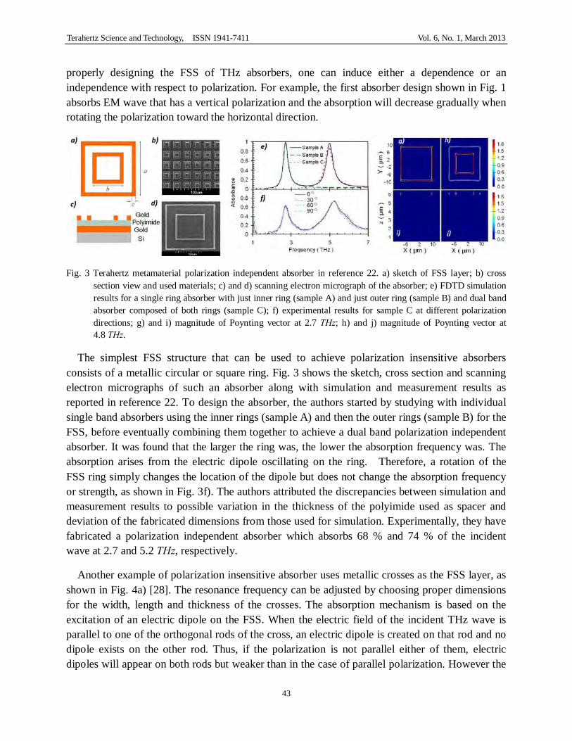
Fig. 3 Terahertz metamaterial polarization independent absorber in reference 22. a) sketch of FSS layer; b) cross section view and used materials; c) and d) scanning electron micrograph of the absorber; e) FDTD simulation results for a single ring absorber with just inner ring (sample A) and just outer ring (sample B) and dual band absorber composed of both rings (sample C); f) experimental results for sample C at different polarization directions; g) and i) magnitude of Poynting vector at 2.7 THz; h) and j) magnitude of Poynting vector at 4.8 THz.
The simplest FSS structure that can be used to achieve polarization insensitive absorbers consists of a metallic circular or square ring. Fig. 3 shows the sketch, cross section and scanning electron micrographs of such an absorber along with simulation and measurement results as reported in reference 22. To design the absorber, the authors started by studying with individual single band absorbers using the inner rings (sample A) and then the outer rings (sample B) for the FSS, before eventually combining them together to achieve a dual band polarization independent absorber. It was found that the larger the ring was, the lower the absorption frequency was. The absorption arises from the electric dipole oscillating on the ring. Therefore, a rotation of the FSS ring simply changes the location of the dipole but does not change the absorption frequency or strength, as shown in Fig. 3f). The authors attributed the discrepancies between simulation and measurement results to possible variation in the thickness of the polyimide used as spacer and deviation of the fabricated dimensions from those used for simulation. Experimentally, they have fabricated a polarization independent absorber which absorbs 68 % and 74 % of the incident wave at 2.7 and 5.2 THz, respectively.
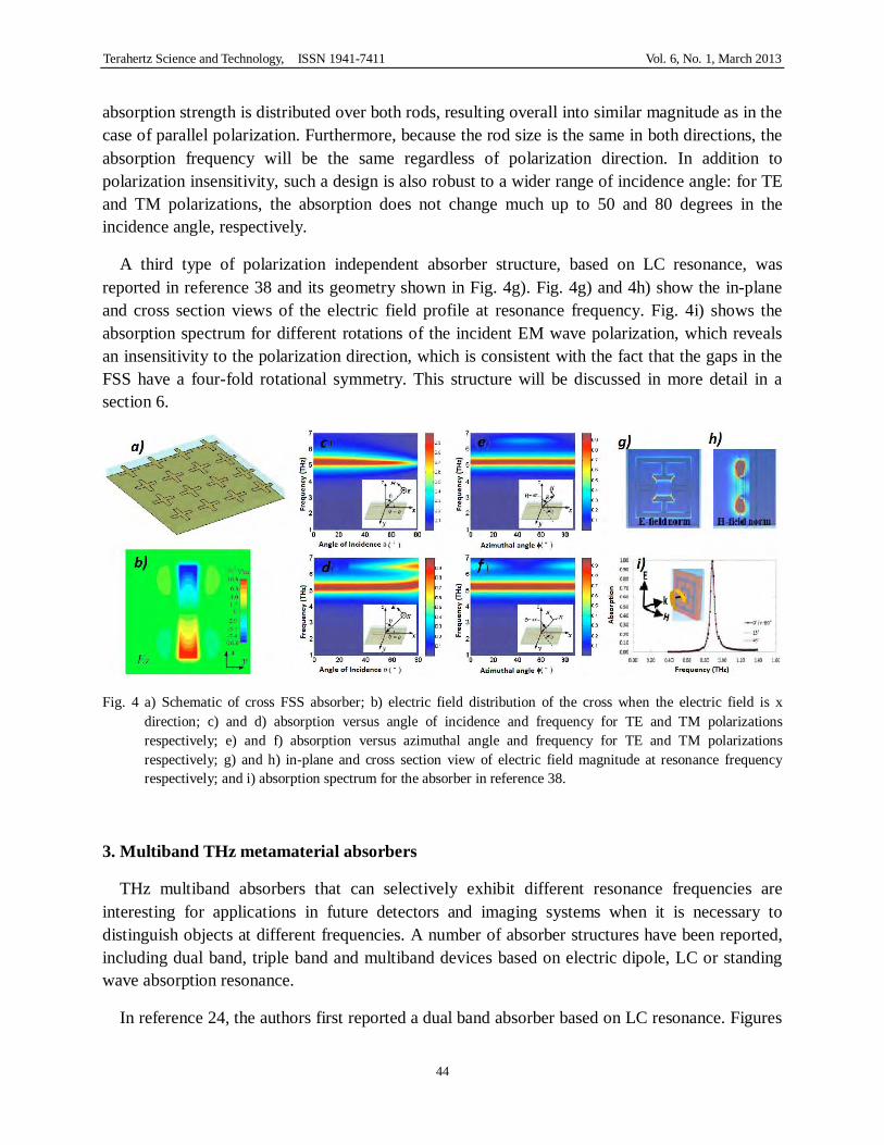
Another example of polarization insensitive absorber uses metallic crosses as the FSS layer, as shown in Fig. 4a) [28]. The resonance frequency can be adjusted by choosing proper dimensions for the width, length and thickness of the crosses. The absorption mechanism is based on the excitation of an electric dipole on the FSS. When the electric field of the incident THz wave is parallel to one of the orthogonal rods of the cross, an electric dipole is created on that rod and no dipole exists on the other rod. Thus, if the polarization is not parallel either of them, electric dipoles will appear on both rods but weaker than in the case of parallel polarization. However the
Terahertz Science and Technology, ISSN 1941-7411 Vol. 6, No. 1, March 2013
44
absorption strength is distributed over both rods, resulting overall into similar magnitude as in the case of parallel polarization. Furthermore, because the rod size is the same in both directions, the absorption frequency will be the same regardless of polarization direction. In addition to polarization insensitivity, such a design is also robust to a wider range of incidence angle: for TE and TM polarizations, the absorption does not change much up to 50 and 80 degrees in the incidence angle, respectively.
A third type of polarization independent absorber structure, based on LC resonance, was reported in reference 38 and its geometry shown in Fig. 4g). Fig. 4g) and 4h) show the in-plane and cross section views of the electric field profile at resonance frequency. Fig. 4i) shows the absorption spectrum for different rotations of the incident EM wave polarization, which reveals an insensitivity to the polarization direction, which is consistent with the fact that the gaps in the FSS have a four-fold rotational symmetry. This structure will be discussed in more detail in a section 6.
Fig. 4 a) Schematic of cross FSS absorber; b) electric field distribution of the cross when the electric field is x direction; c) and d) absorption versus angle of incidence and frequency for TE and TM polarizations respectively; e) and f) absorption versus azimuthal angle and frequency for TE and TM polarizations respectively; g) and h) in-plane and cross section view of electric field magnitude at resonance frequency respectively; and i) absorption spectrum for the absorber in reference 38.
3. Multiband THz metamaterial absorbers
THz multiband absorbers that can selectively exhibit different resonance frequencies are interesting for applications in future detectors and imaging systems when it is necessary to distinguish objects at different frequencies. A number of absorber structures have been reported, including dual band, triple band and multiband devices based on electric dipole, LC or standing wave absorption resonance.
In reference 24, the authors first reported a dual band absorber based on LC resonance. Figures
Terahertz Science and Technology, ISSN 1941-7411 Vol. 6, No. 1, March 2013
45
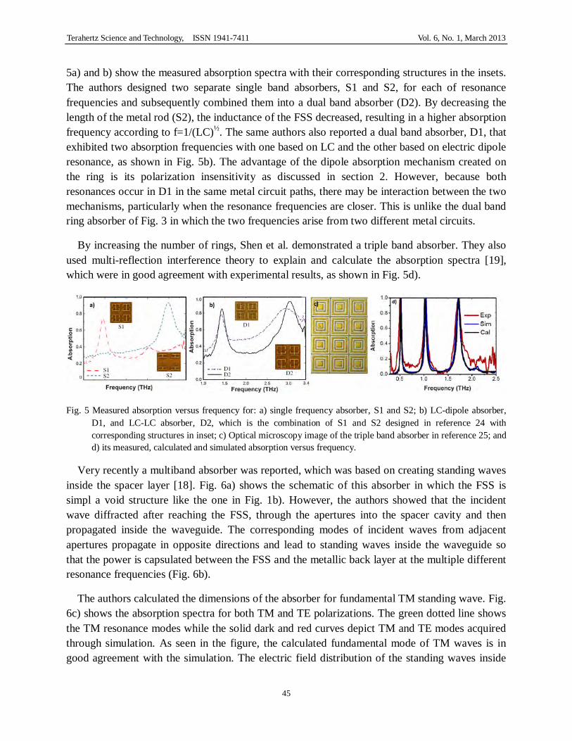
5a) and b) show the measured absorption spectra with their corresponding structures in the insets. The authors designed two separate single band absorbers, S1 and S2, for each of resonance frequencies and subsequently combined them into a dual band absorber (D2). By decreasing the length of the metal rod (S2), the inductance of the FSS decreased, resulting in a higher absorption frequency according to f=1/(LC)½. The same authors also reported a dual band absorber, D1, that exhibited two absorption frequencies with one based on LC and the other based on electric dipole resonance, as shown in Fig. 5b). The advantage of the dipole absorption mechanism created on the ring is its polarization insensitivity as discussed in section 2. However, because both resonances occur in D1 in the same metal circuit paths, there may be interaction between the two mechanisms, particularly when the resonance frequencies are closer. This is unlike the dual band ring absorber of Fig. 3 in which the two frequencies arise from two different metal circuits.
By increasing the number of rings, Shen et al. demonstrated a triple band absorber. They also used multi-reflection interference theory to explain and calculate the absorption spectra [19], which were in good agreement with experimental results, as shown in Fig. 5d).
Fig. 5 Measured absorption versus frequency for: a) single frequency absorber, S1 and S2; b) LC-dipole absorber, D1, and LC-LC absorber, D2, which is the combination of S1 and S2 designed in reference 24 with corresponding structures in inset; c) Optical microscopy image of the triple band absorber in reference 25; and d) its measured, calculated and simulated absorption versus frequency.
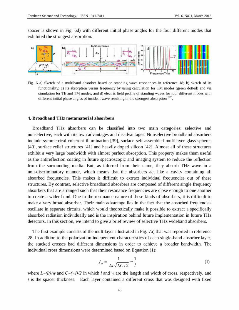
Very recently a multiband absorber was reported, which was based on creating standing waves inside the spacer layer [18]. Fig. 6a) shows the schematic of this absorber in which the FSS is simpl a void structure like the one in Fig. 1b). However, the authors showed that the incident wave diffracted after reaching the FSS, through the apertures into the spacer cavity and then propagated inside the waveguide. The corresponding modes of incident waves from adjacent apertures propagate in opposite directions and lead to standing waves inside the waveguide so that the power is capsulated between the FSS and the metallic back layer at the multiple different resonance frequencies (Fig. 6b).
The authors calculated the dimensions of the absorber for fundamental TM standing wave. Fig. 6c) shows the absorption spectra for both TM and TE polarizations. The green dotted line shows the TM resonance modes while the solid dark and red curves depict TM and TE modes acquired through simulation. As seen in the figure, the calculated fundamental mode of TM waves is in good agreement with the simulation. The electric field distribution of the standing waves inside
Terahertz Science and Technology, ISSN 1941-7411 Vol. 6, No. 1, March 2013
46
spacer is shown in Fig. 6d) with different initial phase angles for the four different modes that exhibited the strongest absorption.
Fig. 6 a) Sketch of a multiband absorber based on standing wave resonances in reference 18; b) sketch of its functionality; c) its absorption versus frequency by using calculation for TM modes (green dotted) and via simulation for TE and TM modes; and d) electric field profile of standing waves for four different modes with different initial phase angles of incident wave resulting in the strongest absorption (18).
4. Broadband THz metamaterial absorbers
Broadband THz absorbers can be classified into two main categories: selective and nonselective, each with its own advantages and disadvantages. Nonselective broadband absorbers include symmetrical coherent illumination [39], surface self assembled multilayer glass spheres [40], surface relief structures [41] and heavily doped silicon [42]. Almost all of these structures exhibit a very large bandwidth with almost perfect absorption. This property makes them useful as the antireflection coating in future spectroscopic and imaging system to reduce the reflection from the surrounding media. But, as inferred from their name, they absorb THz wave in a non-discriminatory manner, which means that the absorbers act like a cavity containing all absorbed frequencies. This makes it difficult to extract individual frequencies out of these structures. By contrast, selective broadband absorbers are composed of different single frequency absorbers that are arranged such that their resonance frequencies are close enough to one another to create a wider band. Due to the resonance nature of these kinds of absorbers, it is difficult to make a very broad absorber. Their main advantage lies in the fact that the absorbed frequencies oscillate in separate circuits, which would theoretically make it possible to extract a specifically absorbed radiation individually and is the inspiration behind future implementation in future THz detectors. In this section, we intend to give a brief review of selective THz wideband absorbers.
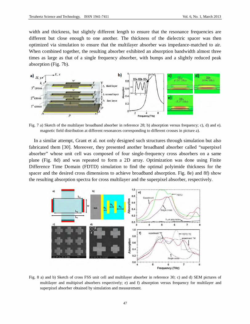
The first example consists of the multilayer illustrated in Fig. 7a) that was reported in reference 28. In addition to the polarization independent characteristics of each single-band absorber layer, the stacked crosses had different dimensions in order to achieve a broader bandwidth. The individual cross dimensions were determined based on Equation (1):
lLCfm
1~2/2
1π
= (1)
where L~(lt)/w and C~(wl)/2 in which l and w are the length and width of cross, respectively, and t is the spacer thickness. Each layer contained a different cross that was designed with fixed
Terahertz Science and Technology, ISSN 1941-7411 Vol. 6, No. 1, March 2013
47
width and thickness, but slightly different length to ensure that the resonance frequencies are different but close enough to one another. The thickness of the dielectric spacer was then optimized via simulation to ensure that the multilayer absorber was impedance-matched to air. When combined together, the resulting absorber exhibited an absorption bandwidth almost three times as large as that of a single frequency absorber, with bumps and a slightly reduced peak absorption (Fig. 7b).
Fig. 7 a) Sketch of the multilayer broadband absorber in reference 28; b) absorption versus frequency; c), d) and e). magnetic field distribution at different resonances corresponding to different crosses in picture a).
In a similar attempt, Grant et al. not only designed such structures through simulation but also fabricated them [30]. Moreover, they presented another broadband absorber called “superpixel absorber” whose unit cell was composed of four single-frequency cross absorbers on a same plane (Fig. 8d) and was repeated to form a 2D array. Optimization was done using Finite Difference Time Domain (FDTD) simulation to find the optimal polyimide thickness for the spacer and the desired cross dimensions to achieve broadband absorption. Fig. 8e) and 8f) show the resulting absorption spectra for cross multilayer and the superpixel absorber, respectively.
Fig. 8 a) and b) Sketch of cross FSS unit cell and multilayer absorber in reference 30; c) and d) SEM pictures of multilayer and multipixel absorbers respectively; e) and f) absorption versus frequency for multilayer and superpixel absorber obtained by simulation and measurement.
Terahertz Science and Technology, ISSN 1941-7411 Vol. 6, No. 1, March 2013
48
The authors attributed the large discrepancy between simulation and experimental measurement in the multilayer structure to potential thickness nonuniformity of the three polyimide layers and discrepancy in the real and assumed value of the polyimide dielectric constant. A comparison of between the simulation results of the two structures reveals that the absorption peak of the multilayer absorber is larger than that of the superpixel absorber. Obviously, this arises from the use of a 2D array in the superpixel absorber: compared to the multilayer absorber, each single frequency absorber in a unit cell can only absorb one fourth of the incident wave, which leads to a reduction in absorption strength.
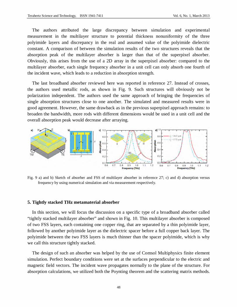
The last broadband absorber reviewed here was reported in reference 27. Instead of crosses, the authors used metallic rods, as shown in Fig. 9. Such structures will obviously not be polarization independent. The authors used the same approach of bringing the frequencies of single absorption structures close to one another. The simulated and measured results were in good agreement. However, the same drawback as in the previous superpixel approach remains: to broaden the bandwidth, more rods with different dimensions would be used in a unit cell and the overall absorption peak would decrease after arraying.
Fig. 9 a) and b) Sketch of absorber and FSS of multilayer absorber in reference 27; c) and d) absorption versus frequency by using numerical simulation and via measurement respectively.
5. Tightly stacked THz metamaterial absorber
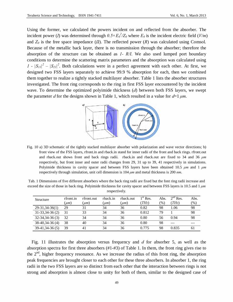
In this section, we will focus the discussion on a specific type of a broadband absorber called “tightly stacked multilayer absorber” and shown in Fig. 10. This multilayer absorber is composed of two FSS layers, each containing one copper ring, that are separated by a thin polyimide layer, followed by another polyimide layer as the dielectric spacer before a full copper back layer. The polyimide between the two FSS layers is much thinner than the spacer polyimide, which is why we call this structure tightly stacked.
The design of such an absorber was helped by the use of Comsol Multiphysics finite element simulation. Perfect boundary conditions were set at the surfaces perpendicular to the electric and magnetic field vectors. The incident wave propagates normally to the plane of the structure. For absorption calculations, we utilized both the Poynting theorem and the scattering matrix methods.
Terahertz Science and Technology, ISSN 1941-7411 Vol. 6, No. 1, March 2013
49
Using the former, we calculated the powers incident on and reflected from the absorber. The incident power (I) was determined through 0.5×E0
2/Z0 where E0 is the incident electric field (V/m) and Z0 is the free space impedance (𝛺). The reflected power (R) was calculated using Comsol. Because of the metallic back layer, there is no transmission through the absorber; therefore the absorption of the structure can be obtained as 1- R/I. We also used lumped port boundary conditions to determine the scattering matrix parameters and the absorption was calculated using 1 - |S11|2 – |S21|2. Both calculations were in a perfect agreement with each other. At first, we designed two FSS layers separately to achieve 99.9 % absorption for each, then we combined them together to realize a tightly stacked multilayer absorber. Table 1 lists the absorber structures investigated. The front ring corresponds to the ring in first FSS layer encountered by the incident wave. To determine the optimized polyimide thickness (d) between both FSS layers, we swept the parameter d for the designs shown in Table 1, which resulted in a value for d=1 μm.
Fig. 10 a) 3D schematic of the tightly stacked multilayer absorber with polarization and wave vector directions; b) front view of the FSS layers, rfront.in and rback.in stand for inner radii of the front and back rings. rfront.out and rback.out shows front and back rings radii. rback.in and rback.out are fixed to 34 and 36 μm respectively, but front inner and outer radii changes from 29, 31 up to 39, 41 respectively in simulations. Polyimide thickness in cavity spacer and between FSS layers have been obtained 10.5 μm and 1 μm respectively through simulation, unit cell dimension is 104 μm and metal thickness is 200 nm.
Tab. 1 Dimensions of five different absorbers where the back ring radii are fixed but the font ring radii increase and exceed the size of those in back ring. Polyimide thickness for cavity spacer and between FSS layers is 10.5 and 1 μm
respectively.
Structure rfront.in (µm)
rfront.out (µm)
rback.in (µm)
rback.out (µm)
1st Res. (THz)
Abs. (%)
2nd Res. (THz)
Abs. (%)
29-31,34-36(1) 29 31 34 36 0.82 98 1.06 98 31-33,34-36 (2) 31 33 34 36 0.812 79 1 98 32-34,34-36 (3) 32 34 34 36 0.80 56 0.94 98 38-40,34-36 (4) 38 40 34 36 0.80 98 --- --- 39-41,34-36 (5) 39 41 34 36 0.775 98 0.835 61
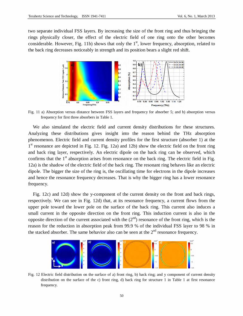
Fig. 11 illustrates the absorption versus frequency and d for absorber 5, as well as the absorption spectra for first three absorbers (#1-#3) of Table 1. In them, the front ring gives rise to the 2nd, higher frequency resonance. As we increase the radius of this front ring, the absorption peak frequencies are brought closer to each other for these three absorbers. In absorber 1, the ring radii in the two FSS layers are so distinct from each other that the interaction between rings is not strong and absorption is almost close to unity for both of them, similar to the designed case of
Terahertz Science and Technology, ISSN 1941-7411 Vol. 6, No. 1, March 2013
50
two separate individual FSS layers. By increasing the size of the front ring and thus bringing the rings physically closer, the effect of the electric field of one ring onto the other becomes considerable. However, Fig. 11b) shows that only the 1st, lower frequency, absorption, related to the back ring decreases noticeably in strength and its position bears a slight red shift.
Fig. 11 a) Absorption versus distance between FSS layers and frequency for absorber 5; and b) absorption versus
frequency for first three absorbers in Table 1.
We also simulated the electric field and current density distributions for these structures. Analyzing these distributions gives insight into the reason behind the THz absorption phenomenon. Electric field and current density profiles for the first structure (absorber 1) at the 1st resonance are depicted in Fig. 12. Fig. 12a) and 12b) show the electric field on the front ring and back ring layer, respectively. An electric dipole on the back ring can be observed, which confirms that the 1st absorption arises from resonance on the back ring. The electric field in Fig. 12a) is the shadow of the electric field of the back ring. The resonant ring behaves like an electric dipole. The bigger the size of the ring is, the oscillating time for electrons in the dipole increases and hence the resonance frequency decreases. That is why the bigger ring has a lower resonance frequency.
Fig. 12c) and 12d) show the y-component of the current density on the front and back rings, respectively. We can see in Fig. 12d) that, at its resonance frequency, a current flows from the upper pole toward the lower pole on the surface of the back ring. This current also induces a small current in the opposite direction on the front ring. This induction current is also in the opposite direction of the current associated with the (2nd) resonance of the front ring, which is the reason for the reduction in absorption peak from 99.9 % of the individual FSS layer to 98 % in the stacked absorber. The same behavior also can be seen at the 2nd resonance frequency.
Fig. 12 Electric field distribution on the surface of a) front ring, b) back ring; and y component of current density
distribution on the surface of the c) front ring, d) back ring for structure 1 in Table 1 at first resonance frequency.
Terahertz Science and Technology, ISSN 1941-7411 Vol. 6, No. 1, March 2013
51
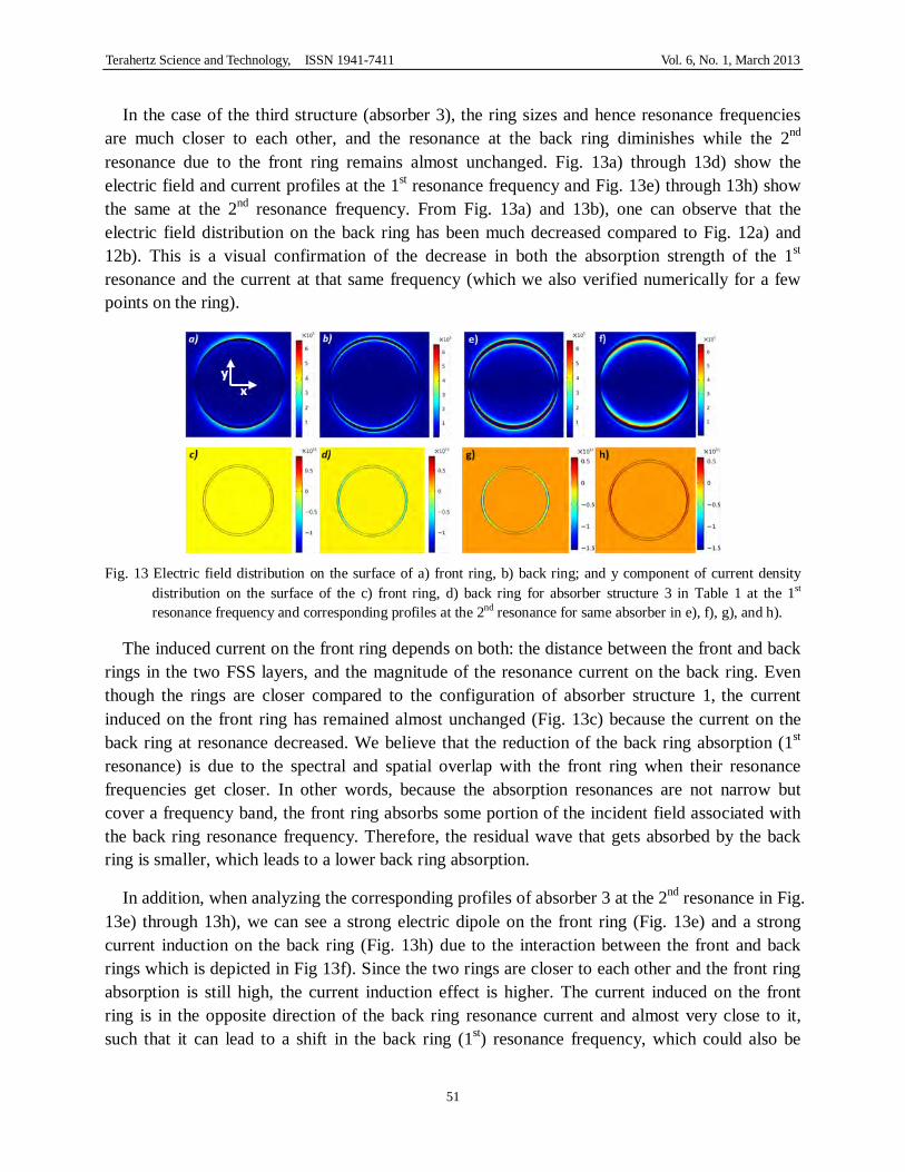
In the case of the third structure (absorber 3), the ring sizes and hence resonance frequencies are much closer to each other, and the resonance at the back ring diminishes while the 2nd resonance due to the front ring remains almost unchanged. Fig. 13a) through 13d) show the electric field and current profiles at the 1st resonance frequency and Fig. 13e) through 13h) show the same at the 2nd resonance frequency. From Fig. 13a) and 13b), one can observe that the electric field distribution on the back ring has been much decreased compared to Fig. 12a) and 12b). This is a visual confirmation of the decrease in both the absorption strength of the 1st resonance and the current at that same frequency (which we also verified numerically for a few points on the ring).
Fig. 13 Electric field distribution on the surface of a) front ring, b) back ring; and y component of current density
distribution on the surface of the c) front ring, d) back ring for absorber structure 3 in Table 1 at the 1st resonance frequency and corresponding profiles at the 2nd resonance for same absorber in e), f), g), and h).
The induced current on the front ring depends on both: the distance between the front and back rings in the two FSS layers, and the magnitude of the resonance current on the back ring. Even though the rings are closer compared to the configuration of absorber structure 1, the current induced on the front ring has remained almost unchanged (Fig. 13c) because the current on the back ring at resonance decreased. We believe that the reduction of the back ring absorption (1st resonance) is due to the spectral and spatial overlap with the front ring when their resonance frequencies get closer. In other words, because the absorption resonances are not narrow but cover a frequency band, the front ring absorbs some portion of the incident field associated with the back ring resonance frequency. Therefore, the residual wave that gets absorbed by the back ring is smaller, which leads to a lower back ring absorption.
In addition, when analyzing the corresponding profiles of absorber 3 at the 2nd resonance in Fig. 13e) through 13h), we can see a strong electric dipole on the front ring (Fig. 13e) and a strong current induction on the back ring (Fig. 13h) due to the interaction between the front and back rings which is depicted in Fig 13f). Since the two rings are closer to each other and the front ring absorption is still high, the current induction effect is higher. The current induced on the front ring is in the opposite direction of the back ring resonance current and almost very close to it, such that it can lead to a shift in the back ring (1st) resonance frequency, which could also be
Terahertz Science and Technology, ISSN 1941-7411 Vol. 6, No. 1, March 2013
52
another factor for the reduction in absorption strength.
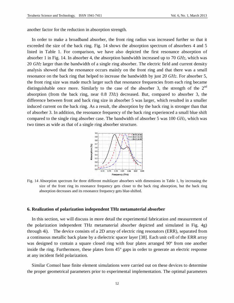
In order to make a broadband absorber, the front ring radius was increased further so that it exceeded the size of the back ring. Fig. 14 shows the absorption spectrum of absorbers 4 and 5 listed in Table 1. For comparison, we have also depicted the first resonance absorption of absorber 1 in Fig. 14. In absorber 4, the absorption bandwidth increased up to 70 GHz, which was 20 GHz larger than the bandwidth of a single ring absorber. The electric field and current density analysis showed that the resonance occurs mainly on the front ring and that there was a small resonance on the back ring that helped to increase the bandwidth by just 20 GHz. For absorber 5, the front ring size was made much larger such that resonance frequencies from each ring became distinguishable once more. Similarly to the case of the absorber 3, the strength of the 2nd absorption (from the back ring, near 0.8 THz) decreased. But, compared to absorber 3, the difference between front and back ring size in absorber 5 was larger, which resulted in a smaller induced current on the back ring. As a result, the absorption by the back ring is stronger than that of absorber 3. In addition, the resonance frequency of the back ring experienced a small blue shift compared to the single ring absorber case. The bandwidth of absorber 5 was 100 GHz, which was two times as wide as that of a single ring absorber structure.
Fig. 14 Absorption spectrum for three different multilayer absorbers with dimensions in Table 1, by increasing the
size of the front ring its resonance frequency gets closer to the back ring absorption, but the back ring absorption decreases and its resonance frequency gets blue-shifted.
6. Realization of polarization independent THz metamaterial absorber
In this section, we will discuss in more detail the experimental fabrication and measurement of the polarization independent THz metamaterial absorber depicted and simulated in Fig. 4g) through 4i). The device consists of a 2D array of electric ring resonators (ERR), separated from a continuous metallic back plane by a dielectric spacer layer [38]. Each unit cell of the ERR array was designed to contain a square closed ring with four plates arranged 90º from one another inside the ring. Furthermore, these plates form 45º gaps in order to generate an electric response at any incident field polarization.
Similar Comsol base finite element simulations were carried out on these devices to determine the proper geometrical parameters prior to experimental implementation. The optimal parameters
Terahertz Science and Technology, ISSN 1941-7411 Vol. 6, No. 1, March 2013
53
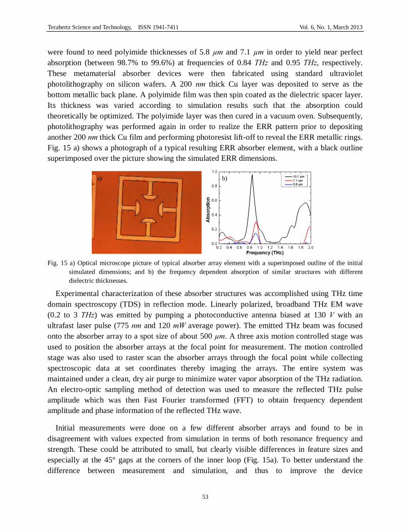
were found to need polyimide thicknesses of 5.8 µm and 7.1 µm in order to yield near perfect absorption (between 98.7% to 99.6%) at frequencies of 0.84 THz and 0.95 THz, respectively. These metamaterial absorber devices were then fabricated using standard ultraviolet photolithography on silicon wafers. A 200 nm thick Cu layer was deposited to serve as the bottom metallic back plane. A polyimide film was then spin coated as the dielectric spacer layer. Its thickness was varied according to simulation results such that the absorption could theoretically be optimized. The polyimide layer was then cured in a vacuum oven. Subsequently, photolithography was performed again in order to realize the ERR pattern prior to depositing another 200 nm thick Cu film and performing photoresist lift-off to reveal the ERR metallic rings. Fig. 15 a) shows a photograph of a typical resulting ERR absorber element, with a black outline superimposed over the picture showing the simulated ERR dimensions.
Fig. 15 a) Optical microscope picture of typical absorber array element with a superimposed outline of the initial
simulated dimensions; and b) the frequency dependent absorption of similar structures with different dielectric thicknesses.
Experimental characterization of these absorber structures was accomplished using THz time domain spectroscopy (TDS) in reflection mode. Linearly polarized, broadband THz EM wave (0.2 to 3 THz) was emitted by pumping a photoconductive antenna biased at 130 V with an ultrafast laser pulse (775 nm and 120 mW average power). The emitted THz beam was focused onto the absorber array to a spot size of about 500 µm. A three axis motion controlled stage was used to position the absorber arrays at the focal point for measurement. The motion controlled stage was also used to raster scan the absorber arrays through the focal point while collecting spectroscopic data at set coordinates thereby imaging the arrays. The entire system was maintained under a clean, dry air purge to minimize water vapor absorption of the THz radiation. An electro-optic sampling method of detection was used to measure the reflected THz pulse amplitude which was then Fast Fourier transformed (FFT) to obtain frequency dependent amplitude and phase information of the reflected THz wave.
Initial measurements were done on a few different absorber arrays and found to be in disagreement with values expected from simulation in terms of both resonance frequency and strength. These could be attributed to small, but clearly visible differences in feature sizes and especially at the 45° gaps at the corners of the inner loop (Fig. 15a). To better understand the difference between measurement and simulation, and thus to improve the device
a) b)
Terahertz Science and Technology, ISSN 1941-7411 Vol. 6, No. 1, March 2013
54
design/realization, we attempted to incorporate these small differences from the actual fabricated arrays. It should also be noted that there was a discrepancy in the conductivity of the Cu metal used in simulation when the size falls under the subwavelength regime compared to that of bulk Cu. A second set of identical devices was then fabricated with the appropriate 10.7 µm polyimide thickness. A comparison of the absorption of the initial devices (5.8 and 7.1 µm polyimide thickness) with the second set of devices (10.7 µm polyimide thickness) is shown in Fig. 15b). The slight differences in feature sizes, along with the change in dielectric thickness, led to a shift in resonance frequency from 0.924 THz to 0.849 THz, as well as an increase in absorption strength from 31 % to 96 % for the new devices with 10.7 µm thick dielectric.
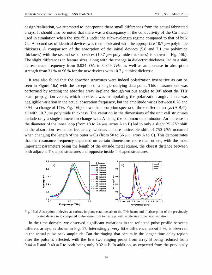
It was also found that the absorber structures were indeed polarization insensitive as can be seen in Figure 16a) with the exception of a single outlying data point. This measurement was performed by rotating the absorber array in-plane through various angles to 90° about the THz beam propagation vector, which in effect, was manipulating the polarization angle. There was negligible variation in the actual absorption frequency, but the amplitude varies between 0.78 and 0.94—a change of 17%. Fig. 16b) shows the absorption spectra of three different arrays (A,B,C), all with 10.7 µm polyimide thickness. The variation in the dimensions of the unit cell structures include only a single dimension change with A being the common denominator. An increase in the diameter of the inner loop (from 18 to 24 µm, array A to B) led to only a slight 25 GHz shift in the absorption resonance frequency, whereas a more noticeable shift of 750 GHz occurred when changing the length of the outer walls (from 50 to 56 µm, array A to C). This demonstrates that the resonance frequency depended on certain dimensions more than others, with the most important parameters being the length of the outside metal square, the closest distance between both adjacent T-shaped structures and opposite inside T-shaped structures.
Fig. 16 a) Absorption of device at various in-plane rotations about the THz beam and b) absorption of the previously
rotated device in a) compared to the same from two arrays with single size dimension variation.
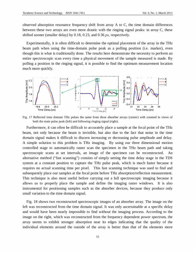
In the time domain, we observed significant variations in the reflected pulse profile between different arrays, as shown in Fig. 17. Interestingly, very little difference, about 5 %, is observed in the actual pulse peak amplitude. But the ringing that occurs in the longer time delay region after the pulse is affected, with the first two ringing peaks from array B being reduced from 0.44 mV and 0.40 mV to both being only 0.32 mV. In addition, as expected from the previously
a) b)
Terahertz Science and Technology, ISSN 1941-7411 Vol. 6, No. 1, March 2013
55
observed absorption resonance frequency shift from array A to C, the time domain differences between these two arrays are even more drastic with the ringing signal peaks: in array C, these shifted sooner (smaller delay) by 0.18, 0.23, and 0.36 ps, respectively.
Experimentally, it is often difficult to determine the optimal placement of the array in the THz beam path when using the time-domain pulse peak as a polling position (i.e. marker), even though this is what is traditionally done. The results here demonstrate the necessity to perform an entire spectroscopic scan every time a physical movement of the sample measured is made. By polling a position in the ringing signal, it is possible to find the optimum measurement location much more quickly.
Fig. 17 Reflected time domain THz pulses the same from three absorber arrays (center) with zoomed in views of
both the main pulse peak (left) and following ringing signal (right).
Furthermore, it can often be difficult to accurately place a sample at the focal point of the THz beam, not only because the beam is invisible, but also due to the fact that noise in the time domain signal makes it difficult to discern increasing or decreasing pulse amplitude and delay. A simple solution to this problem is THz imaging. By using our three dimensional motion controlled stage to automatically raster scan the specimen in the THz beam path and taking spectroscopic scans at set intervals, an image of the specimen can be reconstructed. An alternative method (“fast scanning”) consists of simply setting the time delay stage in the TDS system at a constant position to capture the THz pulse peak, which is much faster because it requires no actual scanning time per pixel. This fast scanning technique was used to find and subsequently place our samples at the focal point before THz absorption/reflection measurement. This technique is also most useful before carrying out a full spectroscopic imaging because it allows us to properly place the sample and define the imaging raster windows. It is also instrumental for positioning samples such as the absorber devices, because they produce only small variation to the time domain signal.
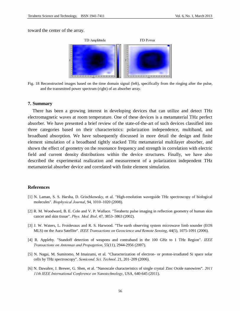
Fig. 18 shows two reconstructed spectroscopic images of an absorber array. The image on the left was reconstructed from the time domain signal. It was only ascertainable at a specific delay and would have been nearly impossible to find without the imaging process. According to the image on the right, which was reconstructed from the frequency dependent power spectrum, the array seems to exhibit stronger absorption near its edges indicating that the quality of the individual elements around the outside of the array is better than that of the elements more
Terahertz Science and Technology, ISSN 1941-7411 Vol. 6, No. 1, March 2013
56
toward the center of the array.
Fig. 18 Reconstructed images based on the time domain signal (left), specifically from the ringing after the pulse,
and the transmitted power spectrum (right) of an absorber array.
7. Summary There has been a growing interest in developing devices that can utilize and detect THz
electromagnetic waves at room temperature. One of these devices is a metamaterial THz perfect absorber. We have presented a brief review of the state-of-the-art of such devices classified into three categories based on their characteristics: polarization independence, multiband, and broadband absorption. We have subsequently discussed in more detail the design and finite element simulation of a broadband tightly stacked THz metamaterial multilayer absorber, and shown the effect of geometry on the resonance frequency and strength in correlation with electric field and current density distributions within the device structures. Finally, we have also described the experimental realization and measurement of a polarization independent THz metamaterial absorber device and correlated with finite element simulation.
References
[1] N. Laman, S. S. Harsha, D. Grischkowsky, et al. "High-resolution waveguide THz spectroscopy of biological molecules". Biophysical Journal, 94, 1010–1020 (2008).
[2] R. M. Woodward, B. E. Cole and V. P. Wallace. "Terahertz pulse imaging in reflection geometry of human skin cancer and skin tissue". Phys. Med. Biol. 47, 3853–3863 (2002).
[3] J. W. Waters, L. Froidevaux and R. S. Harwood. "The earth observing system microwave limb sounder (EOS MLS) on the Aura Satellite". IEEE Transactions on Geoscience and Remote Sensing, 44(5), 1075-1091 (2006).
[4] R. Appleby. "Standoff detection of weapons and contraband in the 100 GHz to 1 THz Region". IEEE Transactions on Antennas and Propagetion, 55(11), 2944-2956 (2007).
[5] N. Nagai, M. Sumitomo, M Imaizumi, et al. "Characterization of electron- or proton-irradiated Si space solar cells by THz spectroscopy". Semicond. Sci. Technol. 21, 201–209 (2006).
[6] N. Dawahre, J. Brewer, G. Shen, et al. "Nanoscale characteristics of single crystal Zinc Oxide nanowires”. 2011 11th IEEE International Conference on Nanotechnology, USA, 640-645 (2011).
Terahertz Science and Technology, ISSN 1941-7411 Vol. 6, No. 1, March 2013
57
[7] B. A. Munk. "Frequency Selective Surfaces: Theory and Design". Wiley(2000).
[8] D. Sievenpiper, L. Zhang, R. F. J. Broas, et al. "High-impedance electromagnetic surfaces with a forbidden frequency band". IEEE Transactions on Microwave Theory and Techniques, 47(11), 2059-2074 (1999).
[9] N. Engheta. "Thin absorbing screens using metamaterial surfaces". IEEE Antennas and Propagation Society International Symposium, 2, 392-395 (2002).
[10] J. Zhang, K. F. MacDonald and N. I. Zheludev. "Controlling light-with-light without nonlinearity". Nature Light: Science and Applications 1, 1-5 (2012).
[11] M. Iwanaga. "Photonic metamaterials: a new class of materials for manipulating light waves". Sci. Technol. Adv. Mater. 13, 053002-053019 (2012).
[12] H. Tao, I. L. Landy, C. M. Bingham, et al. "A metamaterial absorber for terahertz regime: Design, fabrication and characterization". Optics Express, 16(10), 7181-7188 (2008).
[13] D. Schurig, J. J. Mock and D. R. Smith. "Electric-field-coupled resonators for negative permittivity metamaterials". App. Phys. Lett. 88, 041109-1-3 (2006).
[14] L. K. Sun, H. F. Cheng, Y. J. Zhou, et al. "Broadband metamaterial absorber based on coupling resistive frequency selective surface". 20(4), Optics Express, 4675-4980 (2012).
[15] F. Alves, B. Kearney, D. Grbovic, et al. "Strong terahertz absorption using SiO2/Al based metamaterial structures". App. Phys. Lett. 100, 111104-1-3 (2012).
[16] J. Wu and W. Qin. "Terahertz dual-band nearly perfect absorbers based on combined of two types of FSS elements". Microwave Workshop Series on Millimeter Wave Wireless Technology and Applications (IMWS), IEEE MTT-S International, china (2012).
[17] Y. Zeng, H. T. Chen and D. A. R. Dalvit. "A reinterpretation of the metamaterial perfect absorber". arXiv: 1201.5109v1 (2012).
[18] X. Y. Peng, B. Wang, S. Lai, D. H. Zhang, et al. "Ultrathin multi-band planar metamaterial absorber based on standing wave resonances". Optics Express, 20(25), 27756-27765 (2012).
[19] H. T. Chen. "Interference theory of metamaterial perfect absorbers". Optics Express 20(7), 7165-7172, (2012).
[20] H. T. Chen, J. f. Zhou, J. F. O’Hara, et al. "Antireflection coating using metamaterials and identification of its mechanism". PRL, 105, 073901-4 (2010).
[21] H. T. Chen, J. f. Zhou, J. F. O’Hara, et al. "A numerical investigation of metamaterial antireflection coatings". Terahertz Science and Technology, 3(2), 66-73 (2010)
[22] Y. Ma, Q. Chen, Grant, J., Saha, et al. "A terahertz polarization insensitive dual band metamaterial absorber". Optics Letters, 36(6), 945-947 (2011).
[23] X. Shen, T. J. Cui, J. Zhao, et al. "Polarization independent wide-angle triple-band metamaterial absorber". Optics Express, 19(10), 9401-9407 (2011).
[24] H. Tao, C. M. Bingham, D. Pilon, et al. "A dual band terahertz metamaterial absorber". J. Phys. D: App. Phys. 43, 225102-7 (2010).
Terahertz Science and Technology, ISSN 1941-7411 Vol. 6, No. 1, March 2013
58
[25] X. Shen, Y. Yang, Y. Zang, et al. "Triple-band terahertz metamaterial absorber: Design, experiment, and physical interpretation". Appl. Phys. Lett. 101, 154102-1-4 (2012).
[26] Q. Ye, Y. Liu, H. Lin, et al. "Multi-band metamaterial absorber made of multi-gap SRRs structure". App. Phys. A 107, 155–160 (2012).
[27] L. Huang, R. D. Chowdhury, S. Ramani, et al. "Experimental demonstration of terahertz metamaterial absorbers with a broad and flat absorption band". Optics Letters, 37(2), 154-156 (2012).
[28] Y. Q. Ye, Y.Jin and S. He. "Omnidirectional, polarization insensitive and broadband thin absorber in the terahertz regime". J. Opt. Soc. Am. B, 27(3), 498-504 (2010).
[29] J. Sun, L. Liu, G. Dong and J. Zhou. "An extremely broadband metamaterial absorber based on destructive interference". Optics Express, 19(22), 21156-21162 (2011).
[30] James Grant, Yong Ma, Shimul Saha, et al. "Polarization insensitive, broadband terahertz metamaterial absorber". Optics Letters, 36(17), 3476-3478 (2011).
[31] Y. Liu, S. Gu, C. Luo, et al. "Ultra-thin broadband metamaterial absorber". Applied Physics A, 108(1), 19-24 (2012).
[32] C. Zaichun , M. Rahmani , G. Yandong, et al. "Realization of variable three-dimensional terahertz metamaterial tubes for passive resonance tunability". Advanced Optical Materials, 24( 23), 143–147 (2012).
[33] H. Tao, A. C. Strikwerda, K. Fan, et al. "Terahertz metamaterials on free-standing highly-flexible polyimide substrates". J. Phys. D: Appl. Phys. 41, 232004-1-5 (2008).
[34] W. Zhu, Y. Huang, I. D. Rukhlenko, et al. "Configurable metamaterial absorber with pseudo wideband spectrum". Optics Express, 20(6), 6616-6621 (2012).
[35] L. Huang, D. Roy Chowdhury and S. Ramani. "Impact of resonator geometry and its coupling with ground plane on ultrathin metamaterial perfect absorbers". App. Phys. Lett. 101, 101102-1-4 (2012).
[36] J. Wang, C. Fan, P. Ding, et al. "Tunable broad-band perfect absorber by exciting of multiple plasmon resonances at optical frequency". Optics Express, 20(14), 14871-14878 (2012).
[37] H. Y. Zheng, X. R. Jin, J. W. Park, et al. "Tunable dual-band perfect absorbers based on extraordinary optical transmission and Fabry-Perot cavity resonance". Optics Express, 20(21), 24003-24009 (2012).
[38] D. S. Wilbert, M. P. Hokmabadi, W. Baughman, et al. "Highly efficient, polarization insensitive terahertz metamaterial perfect absorber and imaging". Photonics Conference (IPC), 2012 IEEEE, 228-229 (2012).
[39] M. Pu, Q. Feng, M. Wang, et al. "Ultrathin broadband nearly perfect absorber with symmetrical coherent illumination". Optics Express, 20(3), 2246-2254 (2012).
[40] D. S. Kim, D. H. Kim, S. Hwang, et al. "Broadband terahertz absorber realized by self-assembled multilayer glass spheres". Optics Express, 20(12), 13566-13572 (2012).
[41] D. H. Kim, D. S. Kim, S. Hwang, et al. "Surface relief structure for a flexible broadband terahertz absorber". Optics Express, 20(15), 16815-16822 (2012).
[42] M. Pu, M. Wang, C. Hu, et al. "Engineering heavily doped silicon for broadband absorber in the terahertz regime". Optics Express, 20(23) 25513-22519 (2012).