Embed Size (px)
Citation preview

Production sitesGlobal presence

1
2
3
4
5
67

1
2
3
4
5
67
Within the electronics industry, the Cicor Group and its specialized, leading companies play a significant role in various industries around the world. Different industries, different applications, different cultures, but one thing in common: in high demand as high-tech manufacturing partners with a high degree of specialization, unique skills and services.
Cicor is a global engineering and manufacturing service provider with innovative technology solutions for the electronics industry. With 1 841 employees at ten production sites, Cicor manufactures highly complex printed circuit boards, hybrid circuits and 3D-MID solutions and offers complete electronic assembly and plastic injection molding. The Group supplies customized solutions from design to finished product for international customers.
Cicor Group
SwitzerlandBronschhofenBoudryWangs
1RomaniaArad
3GermanyRadebergUlm
2ChinaSuzhou
4VietnamThuan an Town
5SingaporeSingapore
6IndonesiaBatam
7

S.C. Systronics S.R.L manufactures products of consistently high quality using state- of-the-art equipment. The site creates value for its clients through flexibility and a clear focus on solutions.
The production site in Romania offers complete outsourcing solutions for the manufacturing of electronic component assemblies as well as complete devices.
Production site in Arad, RomaniaEl
ectr
onic
Sol
utio
ns
« Complete outsourcing solutions from production to after-sales service.»Floor space: 7,500 m²

Portfolio Test engineering PCB assembly Cable assembly Box building System assembly After-Sales-Service
Markets Automotive Consumer Defense and security Industrial Telecommunication Traffic and transport
Certifications ISO 9001
Quality management system ISO 14001
Environmental management system ISO/TS 16949 Quality management
system for the automotive industry OHSAS 18001 Occupational health
and safety management system
Quality management Recording of all assembled modules
using serial numbers and barcodes (traceability)
Unique barcode on PCBA level for indepth traceability
Recording and analysis via validated quality management system (QDM)
Seamless process monitoring and checks Certified IPC-Trainers
Competencies and servicesEl
ectr
onic
Sol
utio
ns
Traceability PCB barcode laser (Asys) Individual PCBA and component
batch traceability
SMT production Fully automatic in-line printer incl.
stencil cleaning system, automatic optical in-line paste printing inspection
Print image size min. 70 x 60 mm, max. 600 x 450 mm
Adhesive bonding From chip 0603 Adhesive printing
Components Chip up to 0201 (0.5 x 0.25 mm) Fine-pitch assembly up to 0.4 mm
pitch (in serial production) µBGA up to 0.5 mm pitch
Assembly 15 SMD assembly machines
Siplace S-/SX-Series In-line operation
Reflow soldering 5 Nitrogen full convection reflow
systems (SMT) Individual soldering profile Max. reflow soldering width of 460 mm Optical inspection before and after
reflow solderingRework SMD and BGA repair stations
THT productionComponent preparation Automatic cutting Bending, crimping Manual assembly stations
Wave soldering 5 nitrogen wave soldering systems Max. circuit board dimensions of
440 x 390 mm Different, subsequent soldering
programs controlled via barcode Partial soldering with soldering masks Min. circuit board dimension of
95 x 95 mm and max. 400 x 500 mm Timely optical inspection
Process monitoring Soldering profile Wave height Solder bath temperature Regular solder analyses Residual oxygen
Coating Dip coating (KC coating machine) Standard coatings (Peters SL1309N) Silicone coatings
Optical inspection / AOI Inline AOI systems (TRI) with QDM
integration All PCBA are scanned in accordance
with IPC-A-610 Initial sample testing for new projects Serial initial sample testing for each
batch
Box building System assembly Product-specific assembly workplace Functional testing Configurations management
Test Development of product-specific test
concepts In-circuit (Teradyne, TRI), flying probe
(Spea) and functional test (Custom built) Frame scan and boundary scan
implementation Development, construction and
programming of product-specific test systems
High-voltage, run-in and burn-in tests

PT Cicor Panatec is strategically located in Batam, Indonesia, only one hour away from Singapore. This Singapore-Batam combination offers the best of the engineering and management excellence of Singapore and the cost-competitiveness of Batam.
Production site in Batam, IndonesiaEl
ectr
onic
Sol
utio
ns
«State-of-the-art manufacturing facilities combined with highest quality standards.»
Total floor space: 6,740 m²Production molding: 1,630 m²Production assembly: 1,950 m²

Portfolio Plastic injection molding Box building Cleanroom assembly Coil winding
Markets Consumer Industrial Medical technology
Certifications ISO 9001 Quality management system ISO 13485 Quality management system
for medical products ISO/TS 16949 Quality management
system for the automotive industry (from June 2017)
ISO 14001 Environmental management system
OHSAS 18001 Occupational health and safety management system
Manufacturing of Products with UL Cleanroom ISO 8: molding and box
building GMP (good manufacturing practice)
Competencies and servicesEl
ectr
onic
Sol
utio
ns
Plastic injection molding Molding machines ranging from
45 tons to 468 tons Machine types: Engel, Demag,
Netstal, Sumitomo, JSW, Haixing, Haitian and Multiplus
2K molding Insert molding
Assembly/sub-assembly/ cleanroom assembly Precision assembly Miniature assembly Spot welding Ultrasonic welding Coil winding
(wire size: 0.03 mm – 0.70 mm) Pad printing (normal and rotary)
(Max plate size : 100 mm x 100 mm) Vibration welding
Silkscreen printing (max size: 400 mm x 600 mm)
Cleanroom assembly (class 8) Cleanroom molding (class 8)
Services Pre-production to mass production Raw to box-build operation Ultrasonic welding
Test Product reliability test –
humidity/temperature/packaging Salt spray test

Working closely with our customers in the medical, automotive, aerospace & defence, telecommunication and consumer indus-tries, Cicorel SA develops and produces sophisticated rigid, rigid-flexible and flexible printed circuit boards (PCBs) and has com-prehensive expertise in multilayer boards (MLBs), high-density interconnects (HDIs), reel-to-reel technology.
Production site in Boudry, SwitzerlandAd
vanc
ed M
icro
elec
tron
ics
& S
ubst
rate
s
«Guaranteed reliability by being more than a manufacturing partner.»
Floor space: 5,200 m²

Adva
nced
Mic
roel
ectr
onic
s &
Sub
stra
tes
Portfolio Rigid PCBs Rigid-flexible and flexible PCBs MCM HDI Reel-to-reel production Cavities DenciTec®
Markets Aerospace and defense Industrial Medical Telecommunication Testing Watchmaking
Certifications ISO 9001 Quality management system ISO 14001 Environmental management
system OHSAS 18001 Occupational health and
safety management system
Substrates PCBs Rigid, rigid-flexible and flexible PCBs High-density interconnects (HDIs) Multi-chip modules (MCM) 1–32 layer rigid PCBs Multilayer circuits on polyimide,
polyimide glass, LCP, FR-4, high-Tg, HF substrate
Panel and reel-to-reel production Circuit board structures down to
25/25 μm Laser microvias down to 30 µm Mechanical vias down to 75 µm Filled blind vias Stacked/staggered microvias to 6-n-6 +/–5% impedance-controlled circuit
boards Thin base materials down to 12.5 µm Circuit boards down to 4.0 mm thickness Laser cavities Materials for temperature management
Extensive portfolio of surface finishes (Immersion Sn, Immersion Ag, ENIG,
ENEPIG, OSP, ASIG, Galvanic Ni/Au, HASL) Electrical, optical and thermal testing
DenciTec® – new possibilities in miniaturization Line width and spacing as small as
25 micron Copper thickness of 20 ± 5 microns
on all layers Laser via diameters of 35 microns No restrictions in design
Competencies and services

Swisstronics Contract Manufacturing AGdevelops and manufactures products of high quality using state-of-the-art equipment. The site in Bronschhofen offers offer complete outsourcing solutions for the development and manu -facturing of electronic component assemblies as well as complete devices and systems.The site creates value for its customer through flexibility and a clear focus on customer- specific solutions.
Production site in Bronschhofen, SwitzerlandEl
ectr
onic
Sol
utio
ns
« Development and manufacture of customized electronic products.»
Floor space: 6,000 m²

Elec
tron
ic S
olut
ions
Portfolio HW/SW Development PCB layout Test engineering PCB assembly Box building System assembly Medical device assembly After-sales service
Markets Consumer Defense and security Industrial Medical technology Traffic and transport Telecommunication
Certifications ISO 9001 Quality management system ISO 13485 Quality management system
for medical products ISO 14001 Environmental management
system AQAP 2110 – NATO quality assurance
requirements for design, development and production
Production according to IPC A-610D class II and III
Manufacturing of products with UL- registration
FDA registered manufacturing plant
Quality management Recording of all assembled modules
using serial numbers and barcodes (traceability)
Unique barcode on PCBA level for indepth traceability
Recording and analysis via validated quality management system (QDM)
Seamless process monitoring and checks Certified IPC-Trainers Life cycle and obsolescence
management
Traceability PCB barcode laser (Asys) Individual PCBA and component
batch traceability
SMT production Fully automatic in-line printer incl.
stencil cleaning system, automatic optical in-line paste printing inspection
Print image size min. 70 x 60 mm, max. 600 x 450 mm
Adhesive bonding From chip 0603 Adhesive printing
Components Chip up to 01005 (0.4 x 0.2 mm) Fine-pitch assembly up to 0.3 mm
pitch (in serial production) µBGA up to 0.35 mm pitch Flexprint assembly Assembly of THR components
(Through-hole-reflow) PoP assembly (Package-on-Package)
Assembly 9 SMD assembly machines
(Siplace S-/SX-Series, Mydata My100) In-line operation
Reflow soldering 4 Nitrogen full convection reflow
systems (SMT) Individual soldering profile 460 mm max. reflow soldering width
Rework SMD und BGA rework stations
(ZEVAC)
THT productionComponent preparation Automatic cutting Bending, crimping Partially automated assembly stations Manual assembly stations
Wave soldering 2 nitrogen wave soldering systems
(Seho) Max. circuit board dimensions of
440 x 390 mm Different, subsequent soldering
programs controlled via barcode Partial soldering with soldering masks
Selective wave soldering 1 dual port selective soldering system
(Ersa) Min. circuit board dimension of
95 x 95 mm and max. 400 x 500 mmProcess monitoring Soldering profile Wave height Solder bath temperature Regular solder analyses Residual oxygen
Optical inspection / AOIInline AOI systems (Göpel) with QDM integration All flat modules are scanned in accordance with IPC-A-610
Initial sample testing with EFA inspection system
Coating / potting Conformal coating line (Nordson) Standard coating (Humiseal 1B73) Serial potting with PU (2 lines) Epoxy resin and silicone potting UV Adhesive bonding Hotmelt potting Manual coating
Box building System assembly Product-specific assembly workplace Functional testing Configurations management
Test Development of product-specific test
concepts In-circuit (Teradyne, TRI), flying probe
(Spea) and functional test (Custom built) Frame scan and boundary scan
implementation Development and set up of product-
specific test systems High-voltage, run-in and burn-in tests
Competencies and services

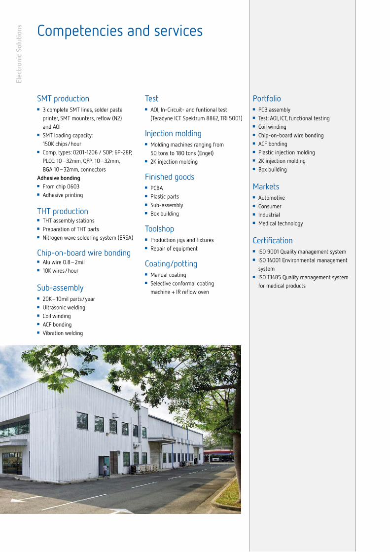
Cicor Anam Ltd. located a mere 20 km from Ho Chi Minh City (Saigon) in the Vietnam- Singapore Industrial Park, hosts the latest, state-of-the-art machinery for printed circuit board assembly (PCBA).
The dedicated team in Thuan an Town is currently serving customers in a variety of sectors, including the medical, industrial, automotive and consumer industries. Cicor Anam Ltd. is ISO 9001, ISO 14001, ISO 13485-certified and comply the RoHS Directive.
Production site in Thuan an Town, VietnamEl
ectr
onic
Sol
utio
ns
«We always strive to offer professional services, advanced design solutions, favorable and reasonable prices, and a punctual delivery.»Floor space: 4,000 m²
Elec
tron
ic S
olut
ions
Portfolio PCB assembly Test: AOI, ICT, functional testing Coil winding Chip-on-board wire bonding ACF bonding Plastic injection molding 2K injection molding Box building
Markets Automotive Consumer Industrial Medical technology
Certification ISO 9001 Quality management system ISO 14001 Environmental management
system ISO 13485 Quality management system
for medical products
SMT production 3 complete SMT lines, solder paste
printer, SMT mounters, reflow (N2) and AOI
SMT loading capacity: 150K chips/hour
Comp. types: 0201-1206 / SOP: 6P-28P, PLCC: 10–32mm, QFP: 10–32mm, BGA 10–32mm, connectors
Adhesive bonding From chip 0603 Adhesive printing
THT production THT assembly stations Preparation of THT parts Nitrogen wave soldering system (ERSA)
Chip-on-board wire bonding Alu wire 0.8–2mil 10K wires/hour
Sub-assembly 20K–10mil parts/year Ultrasonic welding Coil winding ACF bonding Vibration welding
Test AOI, In-Circuit- and funtional test
(Teradyne ICT Spektrum 8862, TRI 5001)
Injection molding Molding machines ranging from
50 tons to 180 tons (Engel) 2K injection molding
Finished goods PCBA Plastic parts Sub-assembly Box building
Toolshop Production jigs and fixtures Repair of equipment
Coating/potting Manual coating Selective conformal coating
machine + IR reflow oven
Competencies and services
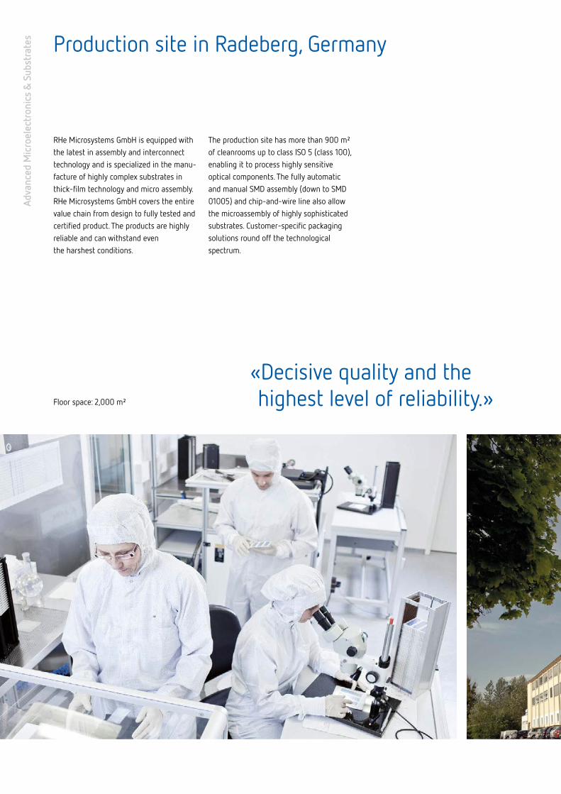
RHe Microsystems GmbH is equipped with the latest in assembly and inter connect technology and is specialized in the manu - facture of highly complex substrates in thick-film technology and micro assembly. RHe Microsystems GmbH covers the entire value chain from design to fully tested and certified product. The products are highly reliable and can withstand even the harshest conditions.
The production site has more than 900 m² of cleanrooms up to class ISO 5 (class 100), enabling it to process highly sensitive optical components. The fully automatic and manual SMD assembly (down to SMD 01005) and chip-and-wire line also allow the microassembly of highly sophisticated substrates. Customer-specific packaging solutions round off the technological spectrum.
Production site in Radeberg, GermanyAd
vanc
ed M
icro
elec
tron
ics
& S
ubst
rate
s
«Decisive quality and the highest level of reliability.»Floor space: 2,000 m²

Adva
nced
Mic
roel
ectr
onic
s &
Sub
stra
tes
Portfolio Thick-film substrates Microassembly Packaging Screening/testing
Markets Aerospace and defense Industrial Medical technology Optoelectronics Research and development Sensors and biosensors Telecommunication
Certifications ISO 9001 Quality management system ISO 13485 Quality management system
for medical products ISO/TS 16949 Quality management
system for the automotive industry EN 9100 Quality management for the
aerospace industry KTA 1401 Quality assurance in nuclear
power plants ESA-PSS-01-606-Qualified manufacture
of thick-film hybrids
Production standards MIL-STD-883 MIL-PRF-38534 ECSS-Q-ST-60-05
Cleanrooms from class ISO 8 to ISO 5 (class 100,000 to 100), 900 m²
Fully and partly automatic bonding machines Thin-wire bonding
Ultrasonic (wedge/wedge) Thermosonic (wedge/wedge,
ball/ wedge) Thick-wire bonding
Ultrasonic (wedge/wedge) Ribbon bonding Thermosonic (wedge/wedge) Beam lead bonding Thermosonic Die bonding Flip chip bonding
Fully automatic and manual SMD assembly line Die attach, COB, flip chip, chip, MMICs,
SMD (min. 01005), (μ)BGA Chip and wire 3D-MID assembly
Packaging Seam welding machine
(hermetic packaging) Circuit protection (passivation, glob top,
paint coating, etc.) MEMS/RF MEMS packaging Vacuum and reflow soldering kiln
Competencies and services

Cicor Ecotool Pte Ltd., thanks to its more than 30 years of experience in the production of high-quality, complex technical molds and plastic parts, is well positioned to offer customers speedy, efficient, cost-effective tool design and fabrication and plastic injection molding.
Production site in Singapore, SingaporeEl
ectr
onic
Sol
utio
ns
«Excellence in tool design, fabrication and injection molding.»Floor space: 2,000 m²

Elec
tron
ic S
olut
ions
Portfolio Tool design and fabrication Plastic injection molding Thin-wall molding Insert Molding
Markets Automotive Consumer Industrial Medical technology
Certifications ISO 9001 Quality management system ISO/TS 16949 Quality management
system for the automotive industry
Tool design Fully integrated advanced 3D software
for mold design and fabrication Unigraphic, AutoCad CAD/CAM software
Plastic injection molding Molding machines ranging from
20 tons to 200 tons High-precision mold with hot runner
system Multi-cavitation design Tool life warranties for up to 1,000,000
shot cycles Thin-wall molding Insert molding
Tool fabrication High-quality European brand machine
(Agie Charmilles, Mikron) Micromolding plastic parts of 2 mm
diameter with micro-structure Critical dimensions control +/–0.02 mm
Quality control High-quality metrology equipment Statistical process control and capability Process control
Competencies and services
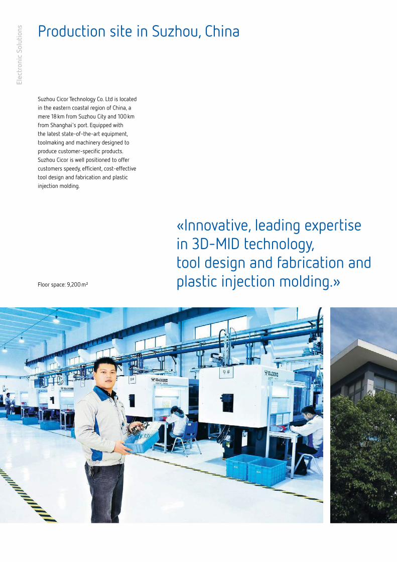
Suzhou Cicor Technology Co. Ltd is located in the eastern coastal region of China, a mere 18 km from Suzhou City and 100 km from Shanghai's port. Equipped with the latest state-of-the-art equipment, toolmaking and machinery designed to produce customer-specific products. Suzhou Cicor is well positioned to offer customers speedy, efficient, cost-effective tool design and fabrication and plastic injection molding.
Production site in Suzhou, ChinaEl
ectr
onic
Sol
utio
ns
«Innovative, leading expertise in 3D-MID technology, tool design and fabrication and plastic injection molding.»Floor space: 9,200 m²

Elec
tron
ic S
olut
ions
Portfolio Tool design and fabrication Plastic injection molding 2K injection molding Insert molding Ultrasonic welding 3D-MID technology
Markets Automotive Consumer Industrial Medical technology
Certifications ISO 9001 Quality management system ISO/TS 16949 Quality management
system for the automotive industry ISO 13485 Quality management system
for medical products Manufacturing of products with
UL- registration
3D-MID technology Miniaturization, tighter
electronic packaging Design flexibility, economization,
environmental compatibility
Tool design and fabrication Advanced CAD-CAM software:
Unigraphic and Pro-E CNC, EDM, wire cutting, grinding,
drilling machine Visual OGP Smartscope, 3D Family
measurement scope, ZPT CMM
Plastic injection molding Injection molding machine with a
range of from 50 tons to 468 tons Material feeding system with
dehumidifier/hopper dryer Swing/traverse robot arm for
all machines 2K injection molding Insert molding
Assembly Ultrasonic welding Pad printing Dehumidifying chamber Sub-assembly Box building
Competencies and services

Reinhardt Microtech GmbH is specialized in the manufacture of highly delicate flexible substrates in thin-film technology and has a very high level of development in this area. Both the manufacture and structuring of base materials (polyimide films) are completed directly on site, with the related processes being constantly developed further.
Reinhardt Microtech GmbH offers its customers a special service in the form of a fast prototyping program, which allows ceramic prototypes to be delivered within 10 working days.
Production site in Ulm, GermanyAd
vanc
ed M
icro
elec
tron
ics
& S
ubst
rate
s
«The continuous development of our technologies is our greatest asset.»Floor space: 1,500 m²

Adva
nced
Mic
roel
ectr
onic
s &
Sub
stra
tes
Portfolio Thin-film substrates Rigid and flexible substrates
(LCP, polyimide) Fast prototyping program
Markets Aerospace and defense Diagnostics Industrial Medical technology Optoelectronics Sensors and biosensors Telecommunication
Certifications ISO 9001 Quality management system
Cleanrooms from class ISO 7 to ISO 5 (class 10,000 to 100), 1,000 m²
Fast prototyping program for ceramic prototypes
Thin-film technology Rigid and flexible substrates, multilayers Metallic coating Sputtering Electroplating (copper, nickel, gold) Photolithography Wet etching, dry etching (RIE)
Automatic laser trimming Laser trimming using a YAG laser High-value resistors
Forming and singulating CO2 laser cutting Diamond cutting
Competencies and services

Production site in Wangs, SwitzerlandAd
vanc
ed M
icro
elec
tron
ics
& S
ubst
rate
s
«Technologically advanced thin-film facility and a flexible set-up for small to high volume production.»
Reinhardt Microtech AG has state-of-the-art production facilities, which are char-acterized by a modular design that allows the site to adapt its capacities to individual customer requirements. The site primarily manufactures rigid and flexible thin-film substrates in small to large volumes, and has cleanroom facilities up to class ISO 5 (class 100).
It also produces high-precision compo-nents for high-frequency applications and products with integrated high-level resistors.
Floor space: 1,300 m²

Adva
nced
Mic
roel
ectr
onic
s &
Sub
stra
tes
Portfolio Thin-film substrates Rigid and flexible substrates
(LCP, polyimide) Set-up for small, medium and
large volume production
Markets Aerospace and defense Diagnostics Industrial Medical technology Optoelectronics Sensors and biosensors Telecommunication
Certifications ISO 9001 Quality management system
Cleanrooms class ISO 7 and ISO 5 (class 10,000 and 100), 660 m²
Thin-film technology Rigid and flexible substrates, multilayers Metallic coating Sputtering Electroplating (copper, nickel, gold) Photolithography Wet etching,
dry etching (RIE) Eutectic AuSn by evaporation
Automatic laser trimming Laser trimming using a YAG laser High-value resistors
Forming and singulating CO2 laser cutting Diamond cutting
Competencies and services

cicor.comCicor Management AGGebenloostrasse 159552 Bronschhofen I Switzerland Tel. +41 71 913 73 00 Fax +41 71 913 73 01 [email protected]
Contact Cicor
EuropeElectronic SolutionsSwisstronics Contract Manufacturing AG Gebenloostrasse 159552 Bronschhofen I SwitzerlandTel. +41 71 913 73 73Fax +41 71 913 73 [email protected]
Advanced Microelectronics & SubstratesCicorel SARoute de l’Europe 82017 Boudry I SwitzerlandTel. +41 32 843 05 00Fax +41 32 843 05 [email protected]
AmericaCicor Americas Inc.185 Alewife Brook Parkway, Suite #410 Cambridge MA 02138 I USATel. +1 617 576 2005Fax +1 617 576 [email protected]
AsiaCicor Asia Pte Ltd.45 Changi South Avenue 2, #02-01Singapore 486133 I SingaporeTel. +65 6546 16 60Fax +65 6546 65 [email protected]