Embed Size (px)
Citation preview
www.IeMRC.org
Martin Goosey
IeMRC Industrial Director
Printed Electronics and Related Projects
supported by the
Innovative Electronics Manufacturing
Research Centre (IeMRC)
www.IeMRC.org
• Overview of the IeMRC
• Printed Electronics and the IeMRC’s projects in this area
• Integrated Optical & Electrical Interconnect PCB Manufacturing
• Smart Microsystems
Presentation Contents
www.IeMRC.org
• The IeMRC is funded by EPSRC
• Part of the Innovative Manufacturing Research Centre programme
• Initially awarded £5.5 million in funding over 5 years
• First period from 2005 to 2010
• Supporting electronics research in academia throughout the UK
The IeMRC
Innovative Electronics Manufacturing Research Centre
www.IeMRC.org
IeMRC Vision Statement
The vision of the IeMRC is to be the UK’s internationally recognised
provider of world-class electronics manufacturing research. It will focus
on sustaining and growing high value manufacturing in the UK by
delivering innovative and exploitable new technologies, highly skilled
people and strategic value to the electronics industry.
www.IeMRC.org
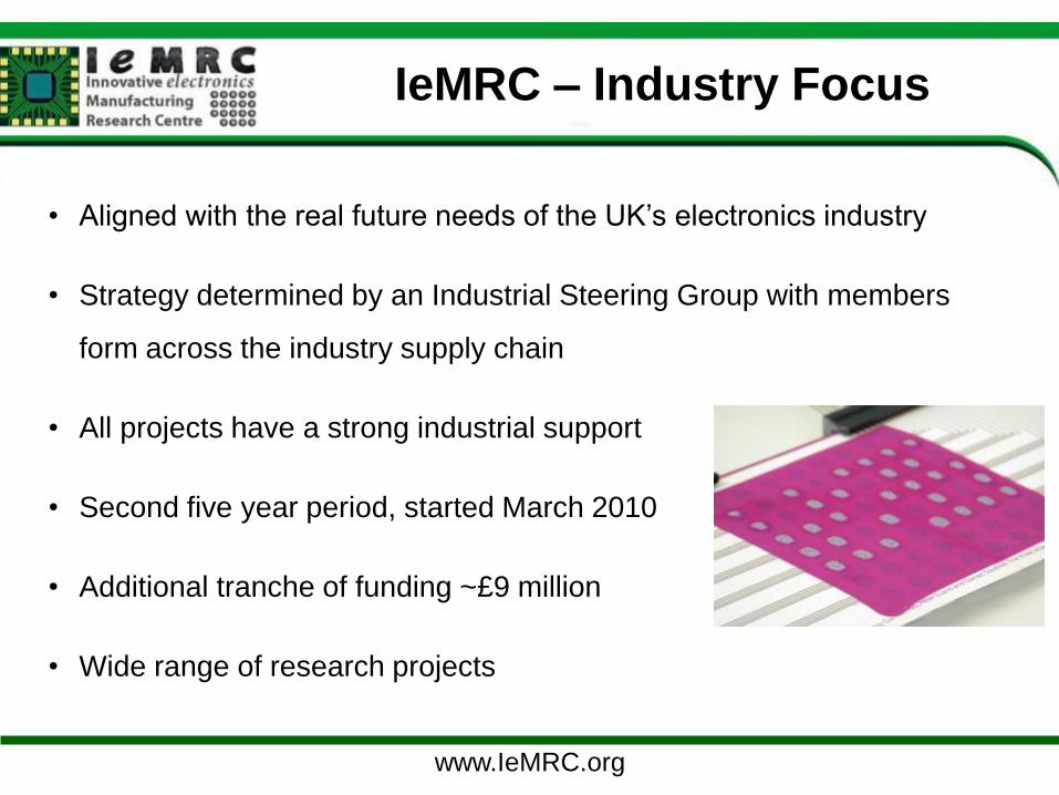
• Aligned with the real future needs of the UK’s electronics industry
• Strategy determined by an Industrial Steering Group with members
form across the industry supply chain
• All projects have a strong industrial support
• Second five year period, started March 2010
• Additional tranche of funding ~£9 million
• Wide range of research projects
IeMRC – Industry Focus
www.IeMRC.org
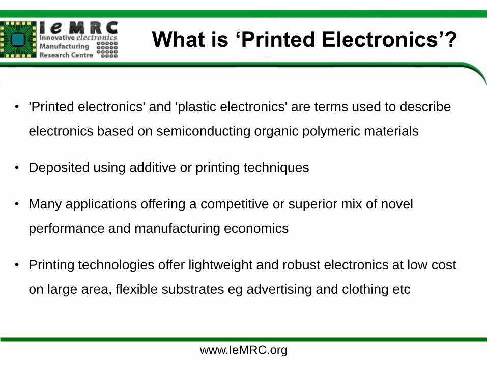
• 'Printed electronics' and 'plastic electronics' are terms used to describe
electronics based on semiconducting organic polymeric materials
• Deposited using additive or printing techniques
• Many applications offering a competitive or superior mix of novel
performance and manufacturing economics
• Printing technologies offer lightweight and robust electronics at low cost
on large area, flexible substrates eg advertising and clothing etc
What is ‘Printed Electronics’?
www.IeMRC.org
• Printed electronics are being developed by by over 3,000 companies,
universities and research institutes worldwide
• Market for printed electronics is beginning to emerge
• This year, the market for printed and thin film electronics is predicted to
reach almost $2.0 billion
• Immediate applications in RFIDs and OLED displays
manufactured using organic thin film transistor technology
Printed Electronics
www.IeMRC.org
• The IeMRC research portfolio is broad and encompasses key areas from
silicon processing through assembly to reliability and end of life issues
• It has supported, and continues to support activities, related to printed
and plastic electronics eg;
− Brunel - lithographic printing of conductors, components, displays
− Surrey - ink jet/spin coating printing of conductive polymers, DTA
− Oxford, Leeds, Manchester and Bangor - new flagship project
IeMRC PE Projects
www.IeMRC.org
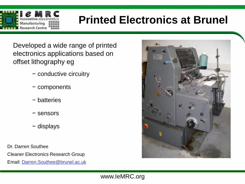
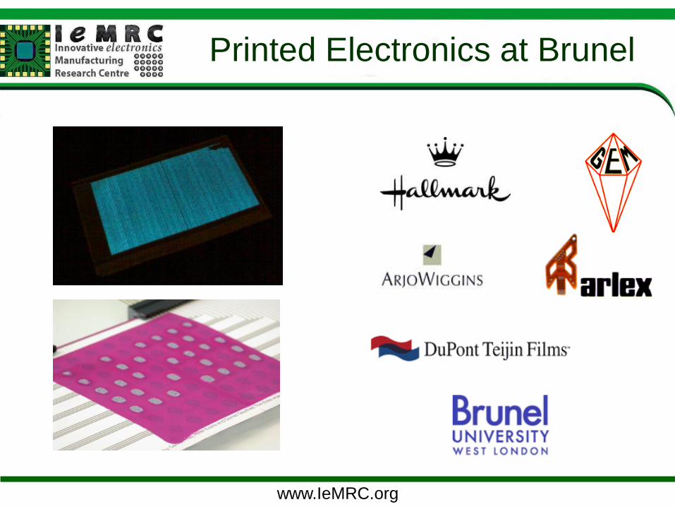
Printed Electronics at Brunel
Developed a wide range of printed
electronics applications based on
offset lithography eg
− conductive circuitry
− components
− batteries
− sensors
− displays
Dr. Darren Southee
Cleaner Electronics Research Group
Email: [email protected]
www.IeMRC.org
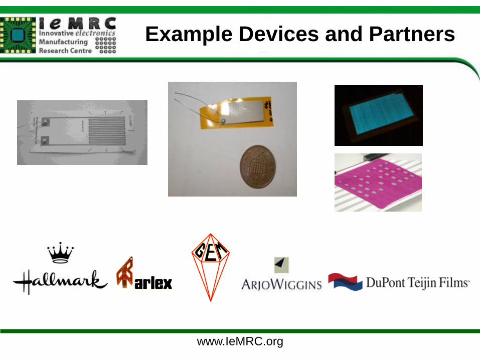
Example Devices and Partners
www.IeMRC.org
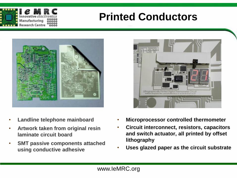
Printed Conductors
• Microprocessor controlled thermometer
• Circuit interconnect, resistors, capacitors
and switch actuator, all printed by offset
lithography
• Uses glazed paper as the circuit substrate
• Landline telephone mainboard
• Artwork taken from original resin
laminate circuit board
• SMT passive components attached
using conductive adhesive
www.IeMRC.org
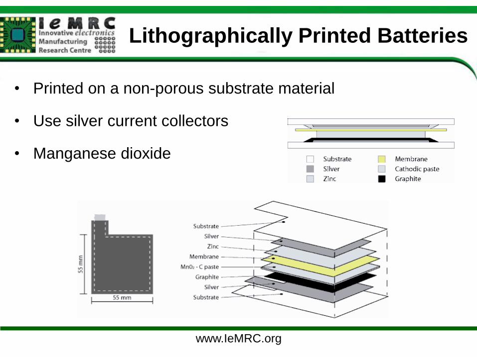
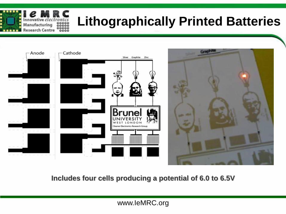
Lithographically Printed Batteries
• Printed on a non-porous substrate material
• Use silver current collectors
• Manganese dioxide
www.IeMRC.org
Lithographically Printed Batteries
Includes four cells producing a potential of 6.0 to 6.5V
www.IeMRC.org
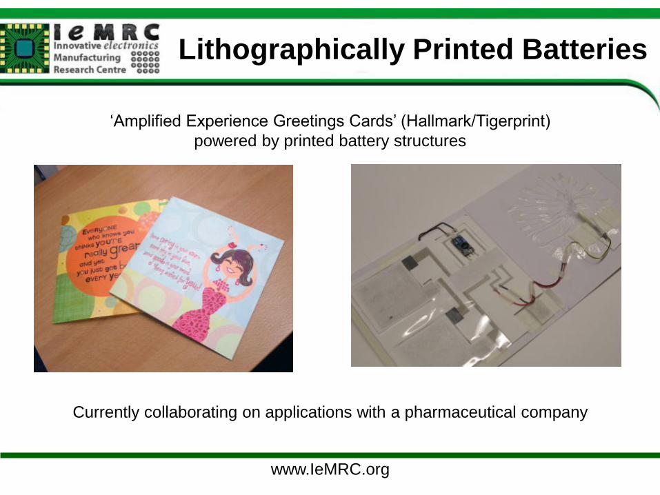
Lithographically Printed Batteries
‘Amplified Experience Greetings Cards’ (Hallmark/Tigerprint)
powered by printed battery structures
Currently collaborating on applications with a pharmaceutical company
www.IeMRC.org
Printed Electronics at Brunel
www.IeMRC.org
Printed Electronics at Surrey
Ink Jet Printing and Spin-Coating
of
Electrically Conductive Polymers
Peter Wilson, Constantina Lekakou and John Watts
www.IeMRC.org
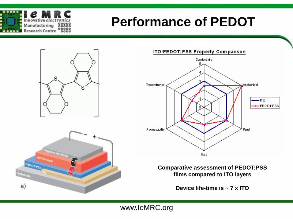
Performance of PEDOT
Comparative assessment of PEDOT:PSS
films compared to ITO layers
Device life-time is ~ 7 x ITO
www.IeMRC.org
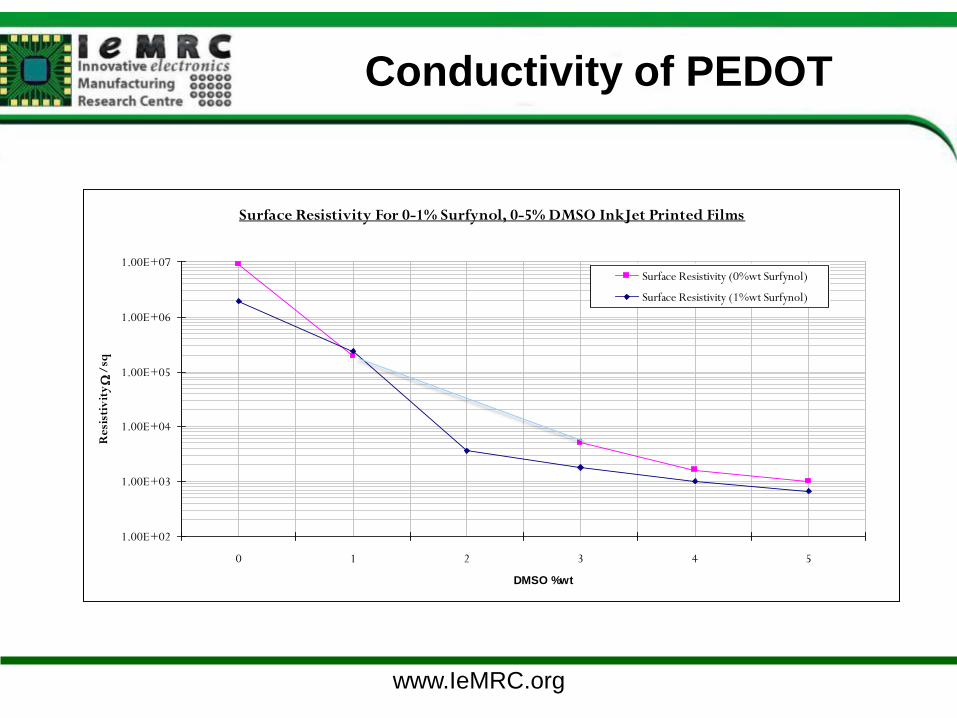
Conductivity of PEDOT
Surface Resistivity For 0-1% Surfynol, 0-5% DMSO InkJet Printed Films
1.00E+02
1.00E+03
1.00E+04
1.00E+05
1.00E+06
1.00E+07
0 1 2 3 4 5
DMSO %wt
Res
isti
vit
y W
/sq
Surface Resistivity (0%wt Surfynol)
Surface Resistivity (1%wt Surfynol)
www.IeMRC.org
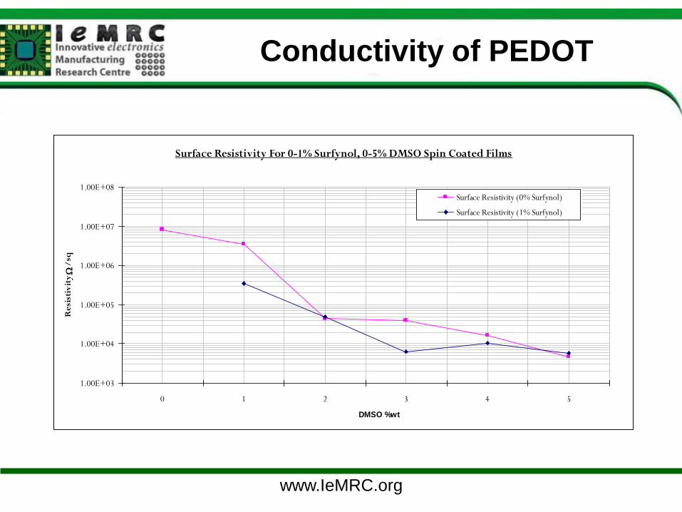
Conductivity of PEDOT
Surface Resistivity For 0-1% Surfynol, 0-5% DMSO Spin Coated Films
1.00E+03
1.00E+04
1.00E+05
1.00E+06
1.00E+07
1.00E+08
0 1 2 3 4 5
DMSO %wt
Re
sist
ivit
y W
/sq
Surface Resistivity (0% Surfynol)
Surface Resistivity (1% Surfynol)
www.IeMRC.org
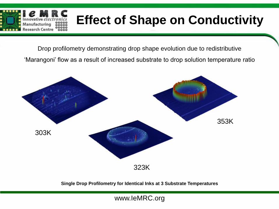
Effect of Shape on Conductivity
Drop profilometry demonstrating drop shape evolution due to redistributive
‘Marangoni’ flow as a result of increased substrate to drop solution temperature ratio
303K
323K
353K
Single Drop Profilometry for Identical Inks at 3 Substrate Temperatures
www.IeMRC.org
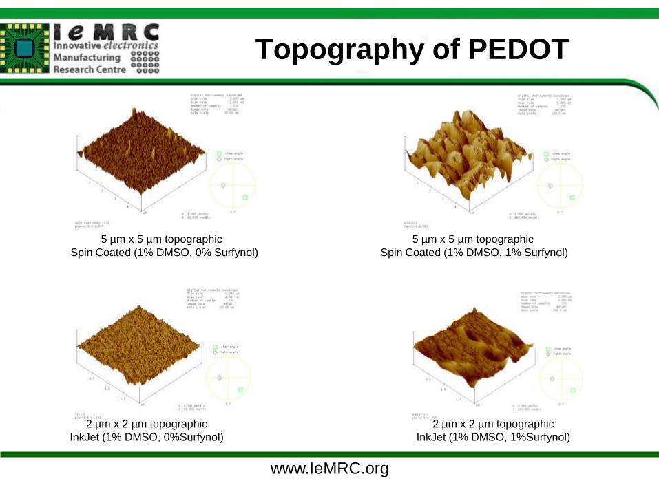
Topography of PEDOT
5 µm x 5 µm topographic
Spin Coated (1% DMSO, 0% Surfynol)
5 µm x 5 µm topographic
Spin Coated (1% DMSO, 1% Surfynol)
2 µm x 2 µm topographic
InkJet (1% DMSO, 0%Surfynol)
2 µm x 2 µm topographic
InkJet (1% DMSO, 1%Surfynol)
www.IeMRC.org
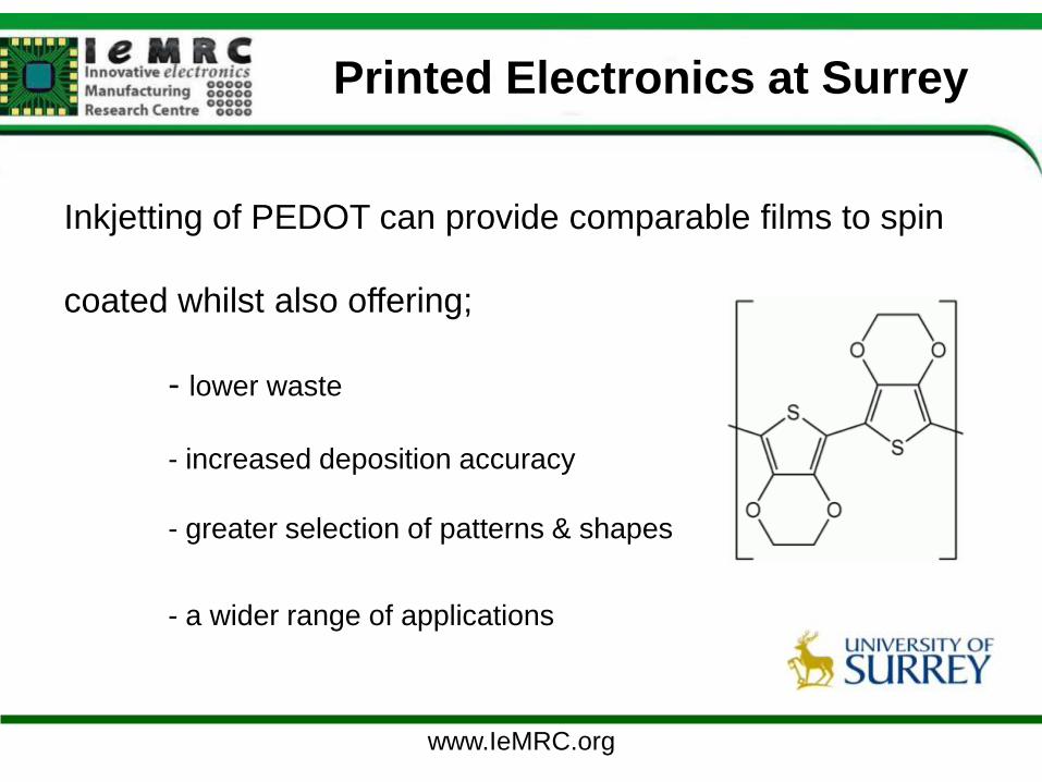
Printed Electronics at Surrey
Inkjetting of PEDOT can provide comparable films to spin
coated whilst also offering;
- lower waste
- increased deposition accuracy
- greater selection of patterns & shapes
- a wider range of applications
www.IeMRC.org
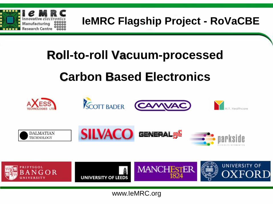
IeMRC Flagship Project - RoVaCBE
Roll-to-roll Vacuum-processed
Carbon Based Electronics
DALMATIAN TECHNOLOGY
www.IeMRC.org
The RoVACBE Flagship Project
• Processing devices and device arrays for properties and high yield
• Link manufacturing parameters and materials with circuit design
• Exploitation of new materials
• Create 2D semiconductor and insulator patterning within a vacuum
R2R process
• Address the mechanical and electrical robustness of the devices
Key Objectives
www.IeMRC.org
Vacuum Deposition of Electronics
• Used for very low-cost simple electronics devices eg
− tagging devices on packaging
− brand protection, product tracking
− anti-counterfeiting for consumer goods
• Extending the existing high-value manufacturing technology
• Vacuum deposition is widely used by the food packaging industry
• Roll-to-roll process with high webspeed (e.g. 50 m/min)
• Low environmental impact process (solventless)
www.IeMRC.org
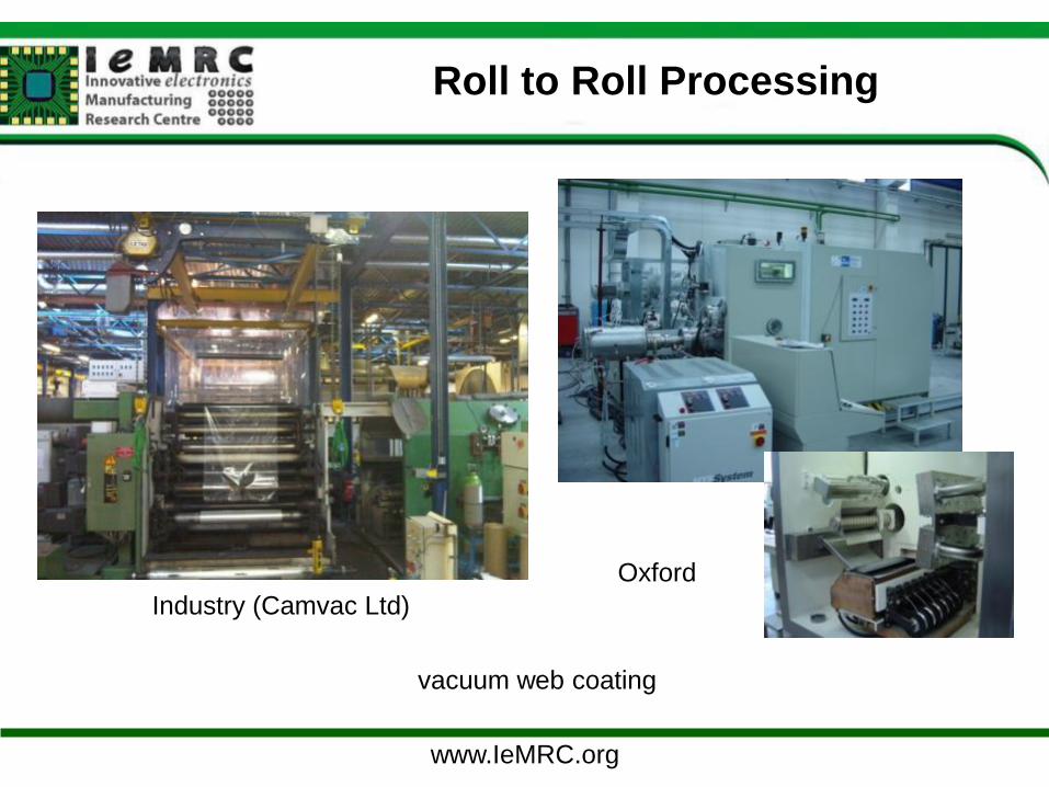
Roll to Roll Processing
vacuum web coating
Industry (Camvac Ltd)
Oxford
www.IeMRC.org
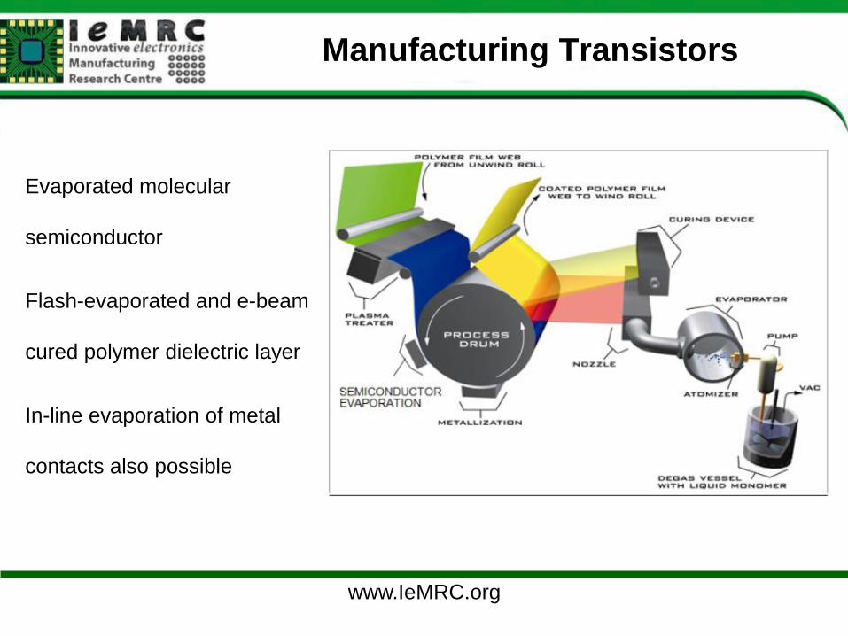
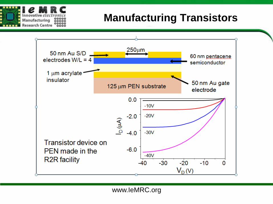
Manufacturing Transistors
Evaporated molecular
semiconductor
Flash-evaporated and e-beam
cured polymer dielectric layer
In-line evaporation of metal
contacts also possible
www.IeMRC.org
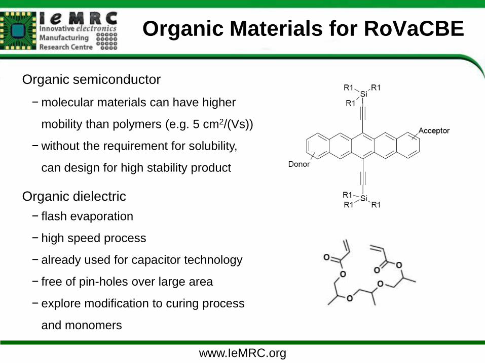
Organic Materials for RoVaCBE
Organic semiconductor
− molecular materials can have higher
mobility than polymers (e.g. 5 cm2/(Vs))
− without the requirement for solubility,
can design for high stability product
Organic dielectric
− flash evaporation
− high speed process
− already used for capacitor technology
− free of pin-holes over large area
− explore modification to curing process
and monomers
www.IeMRC.org
Manufacturing Transistors
www.IeMRC.org
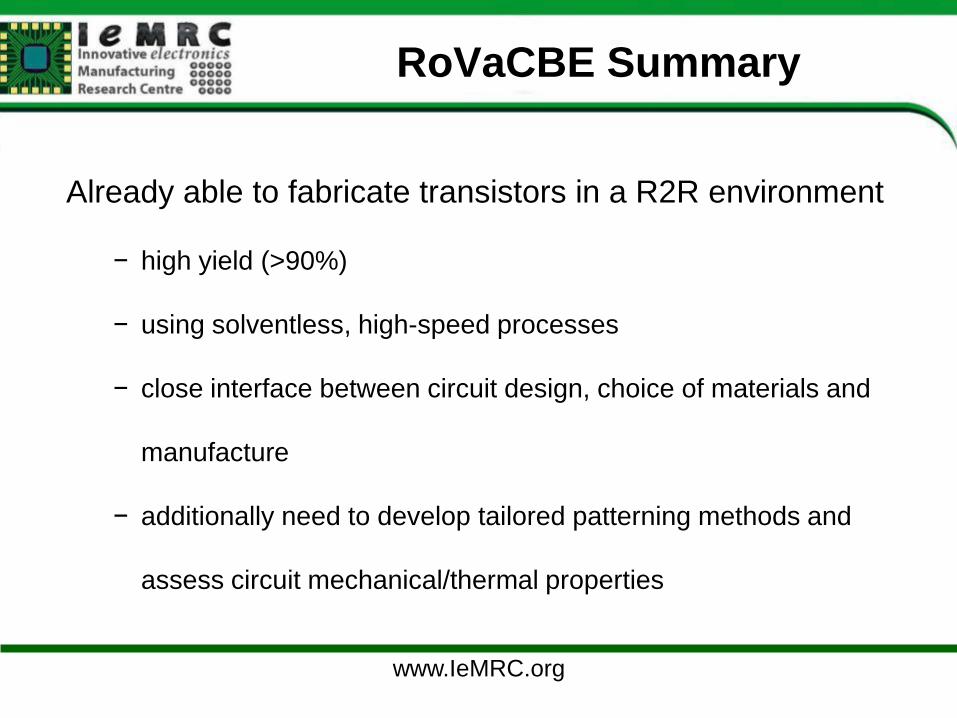
RoVaCBE Summary
Already able to fabricate transistors in a R2R environment
− high yield (>90%)
− using solventless, high-speed processes
− close interface between circuit design, choice of materials and
manufacture
− additionally need to develop tailored patterning methods and
assess circuit mechanical/thermal properties
www.IeMRC.org
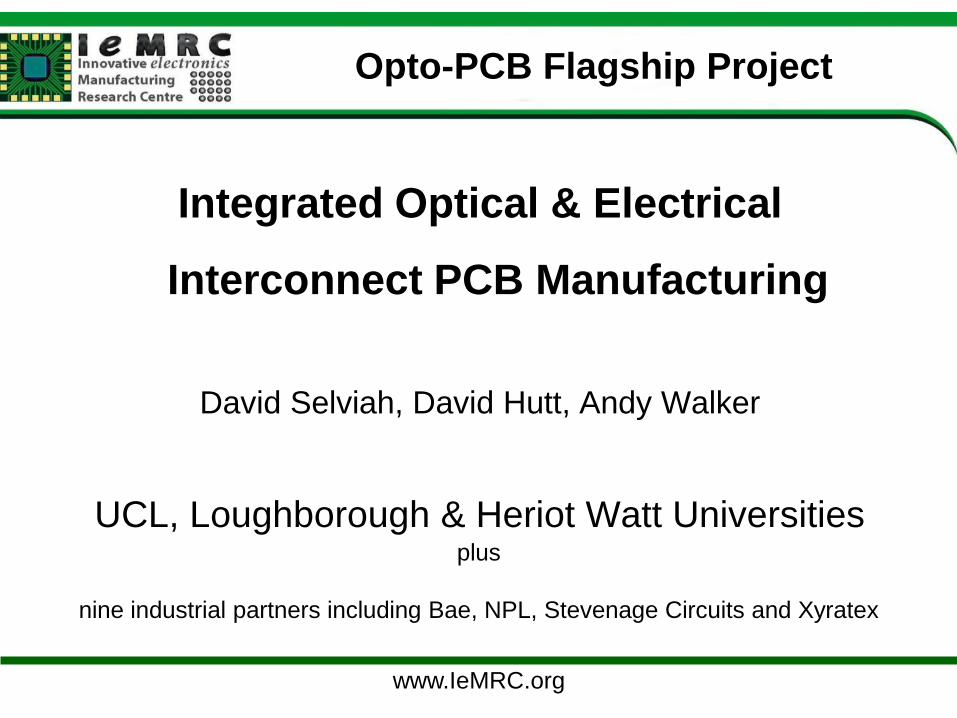
Opto-PCB Flagship Project
Integrated Optical & Electrical
Interconnect PCB Manufacturing
David Selviah, David Hutt, Andy Walker
UCL, Loughborough & Heriot Watt Universitiesplus
nine industrial partners including Bae, NPL, Stevenage Circuits and Xyratex
www.IeMRC.org
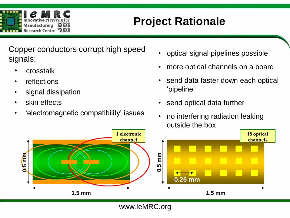
Copper conductors corrupt high speed
signals:
• crosstalk
• reflections
• signal dissipation
• skin effects
• ‘electromagnetic compatibility’ issues
Project Rationale
0.25 mm
1.5 mm
0.25 mm
1.5 mm
0.5
mm
18 optical channels
0.5
mm
1 electronic channel
• optical signal pipelines possible
• more optical channels on a board
• send data faster down each optical
‘pipeline’
• send optical data further
• no interfering radiation leaking
outside the box
www.IeMRC.org
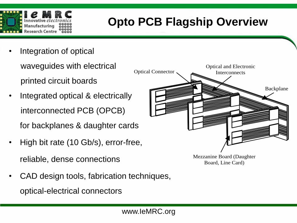
Opto PCB Flagship Overview
Optical and Electronic
Interconnects
Backplane
Mezzanine Board (Daughter
Board, Line Card)
Optical Connector
• Integration of optical
waveguides with electrical
printed circuit boards
• Integrated optical & electrically
interconnected PCB (OPCB)
for backplanes & daughter cards
• High bit rate (10 Gb/s), error-free,
reliable, dense connections
• CAD design tools, fabrication techniques,
optical-electrical connectors
www.IeMRC.org
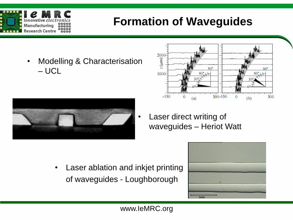
Formation of Waveguides
• Modelling & Characterisation
– UCL
• Laser ablation and inkjet printing
of waveguides - Loughborough
1mm
• Laser direct writing of
waveguides – Heriot Watt
www.IeMRC.org
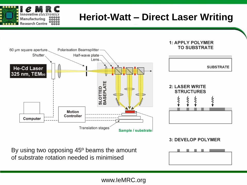
Heriot-Watt – Direct Laser Writing
By using two opposing 45º beams the amount
of substrate rotation needed is minimised
www.IeMRC.org
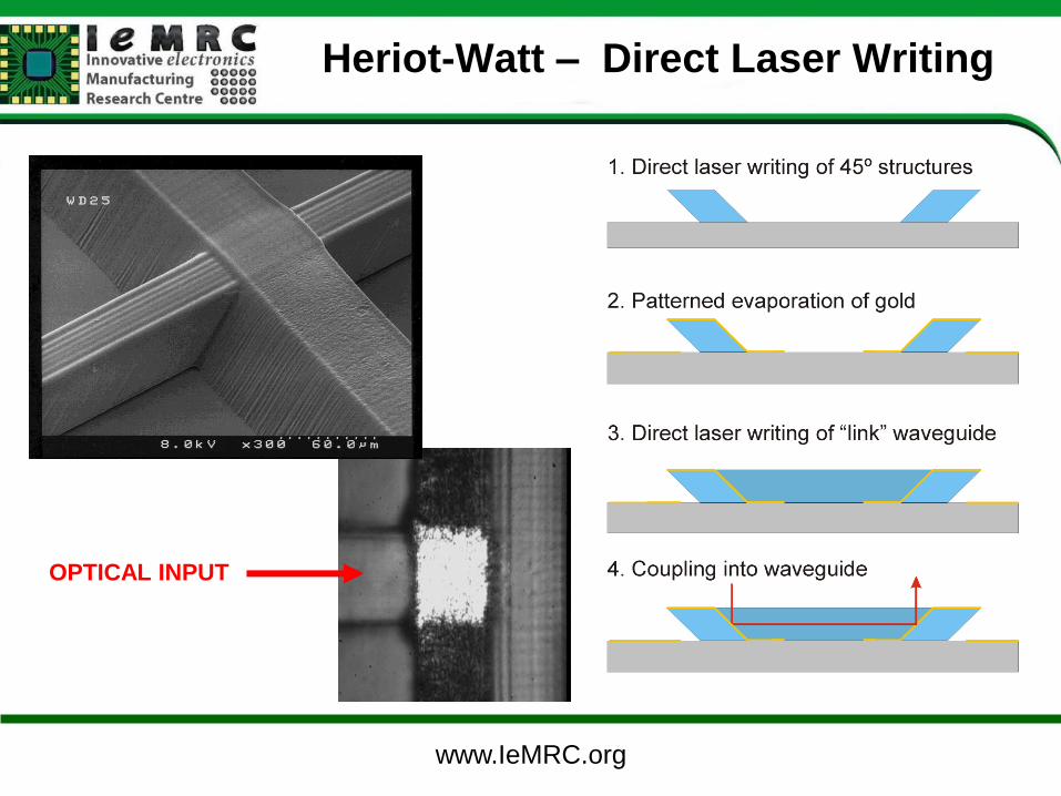
Heriot-Watt – Direct Laser Writing
OPTICAL INPUT
www.IeMRC.org
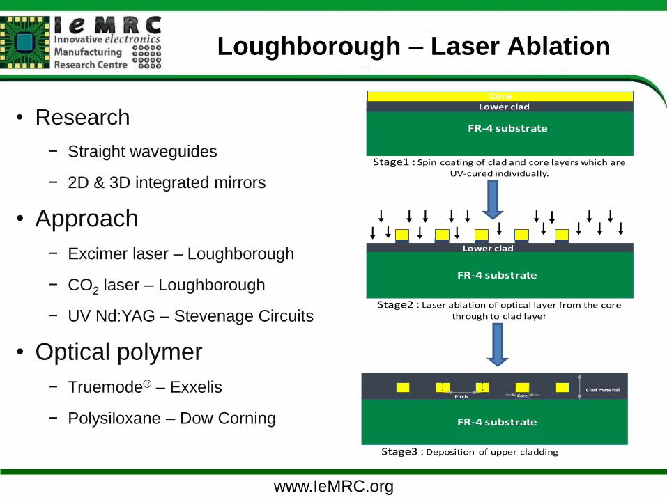
Loughborough – Laser Ablation
• Research
− Straight waveguides
− 2D & 3D integrated mirrors
• Approach
− Excimer laser – Loughborough
− CO2 laser – Loughborough
− UV Nd:YAG – Stevenage Circuits
• Optical polymer
− Truemode® – Exxelis
− Polysiloxane – Dow Corning
Stage1 : Spin coating of clad and core layers which are
UV-cured individually.
Stage2 : Laser ablation of optical layer from the core through to clad layer
Stage3 : Deposition of upper cladding
FR-4 substrate
Lower clad Core
Pitch
Clad materialCore
FR-4 substrate
FR-4 substrate
Lower clad
www.IeMRC.org
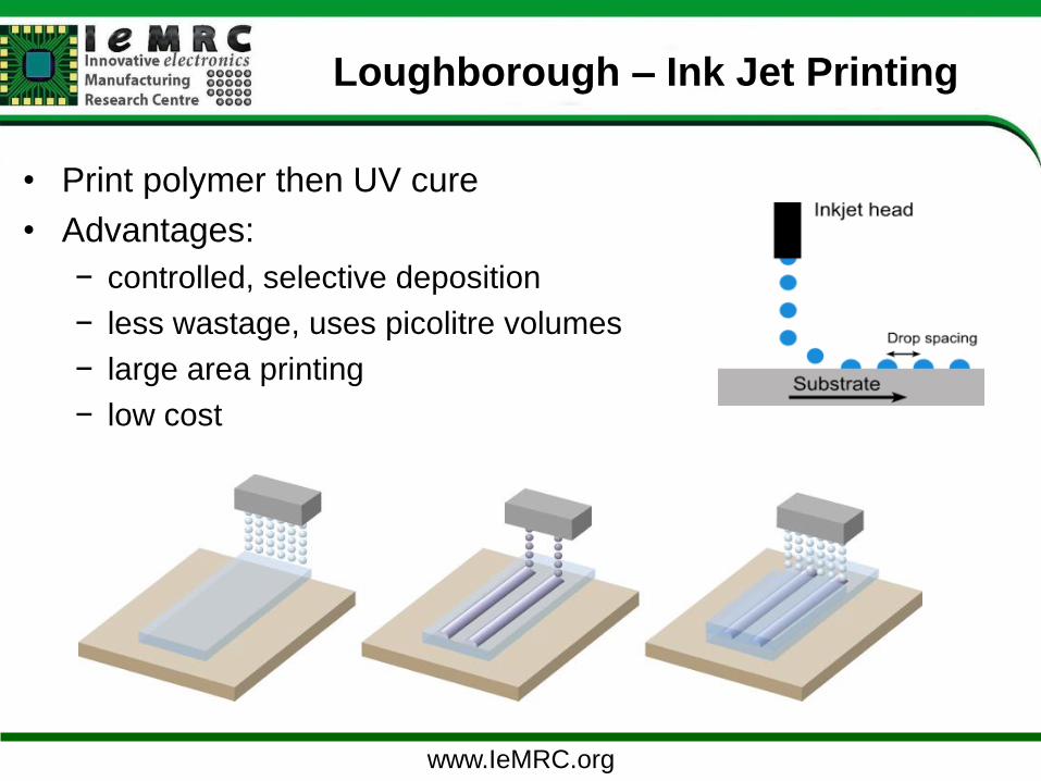
Loughborough – Ink Jet Printing
• Print polymer then UV cure
• Advantages:
− controlled, selective deposition
− less wastage, uses picolitre volumes
− large area printing
− low cost
www.IeMRC.org
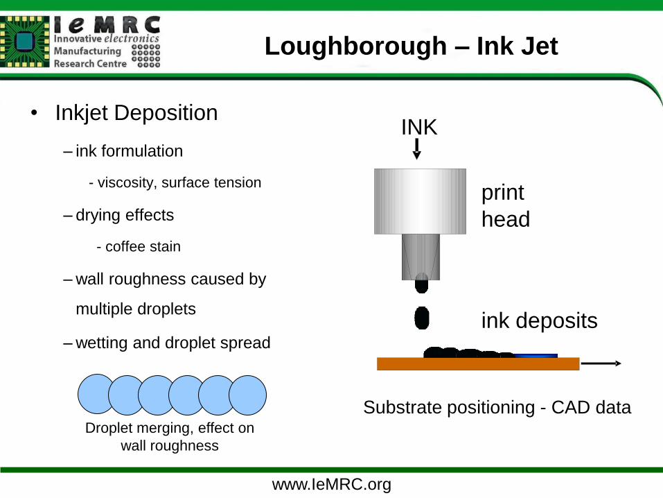
Loughborough – Ink Jet
• Inkjet Deposition
– ink formulation
- viscosity, surface tension
– drying effects
- coffee stain
– wall roughness caused by
multiple droplets
– wetting and droplet spread
Droplet merging, effect on
wall roughness
INK
head
ink deposits
Substrate positioning - CAD data
www.IeMRC.org
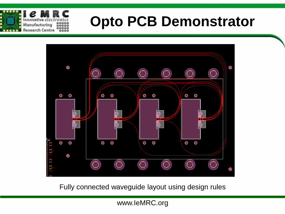
Opto PCB Demonstrator
Fully connected waveguide layout using design rules
www.IeMRC.org
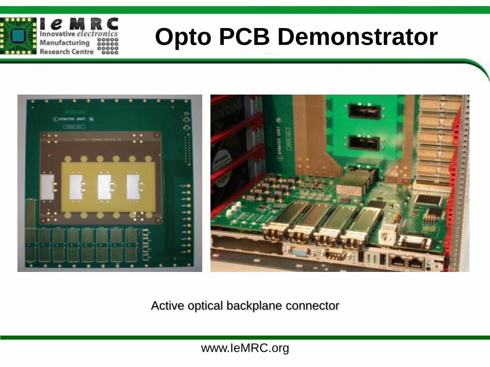
Opto PCB Demonstrator
Active optical backplane connector
www.IeMRC.org
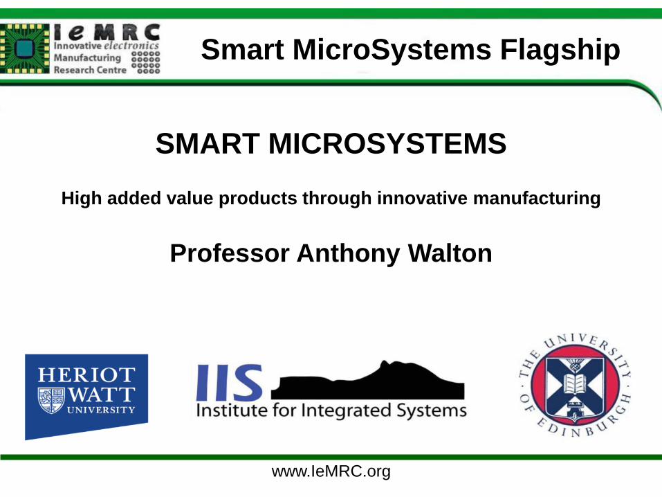
Smart MicroSystems Flagship
SMART MICROSYSTEMS
High added value products through innovative manufacturing
Professor Anthony Walton
www.IeMRC.org
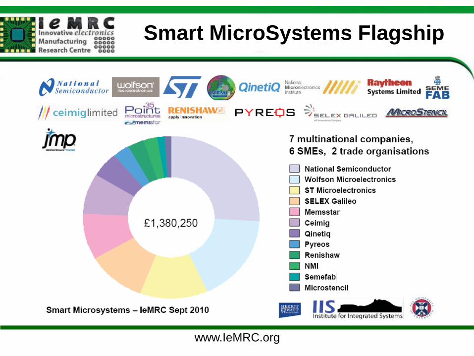
Smart MicroSystems Flagship
www.IeMRC.org
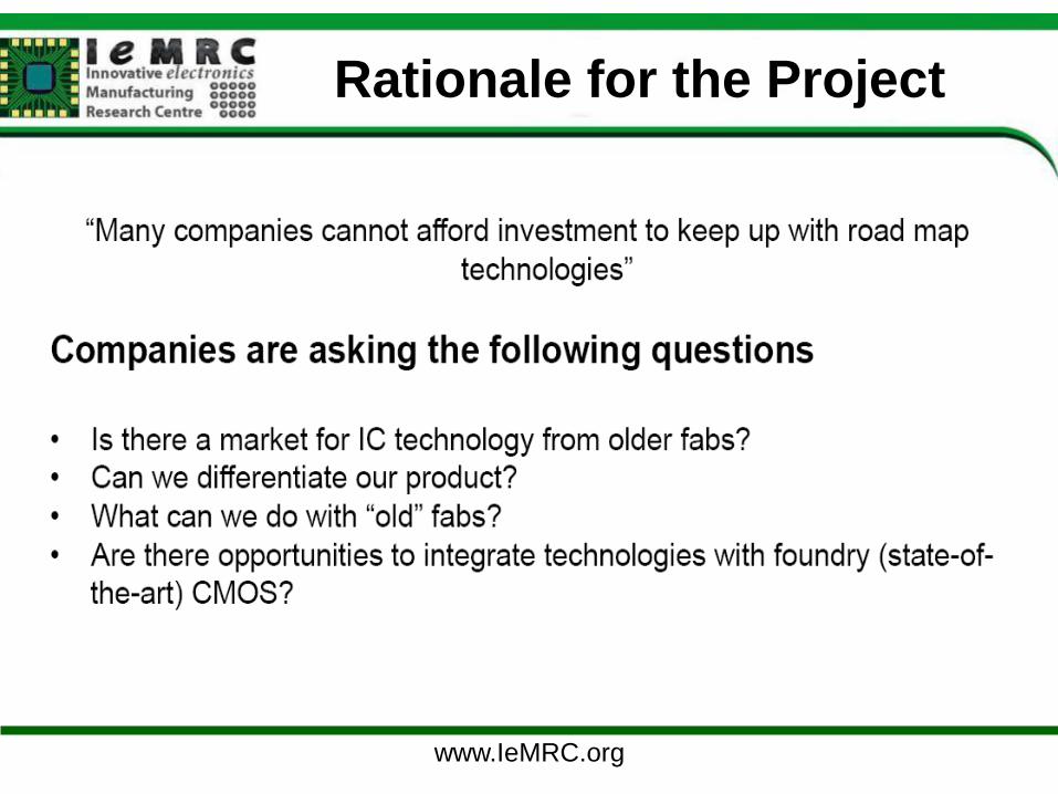
Rationale for the Project
www.IeMRC.org
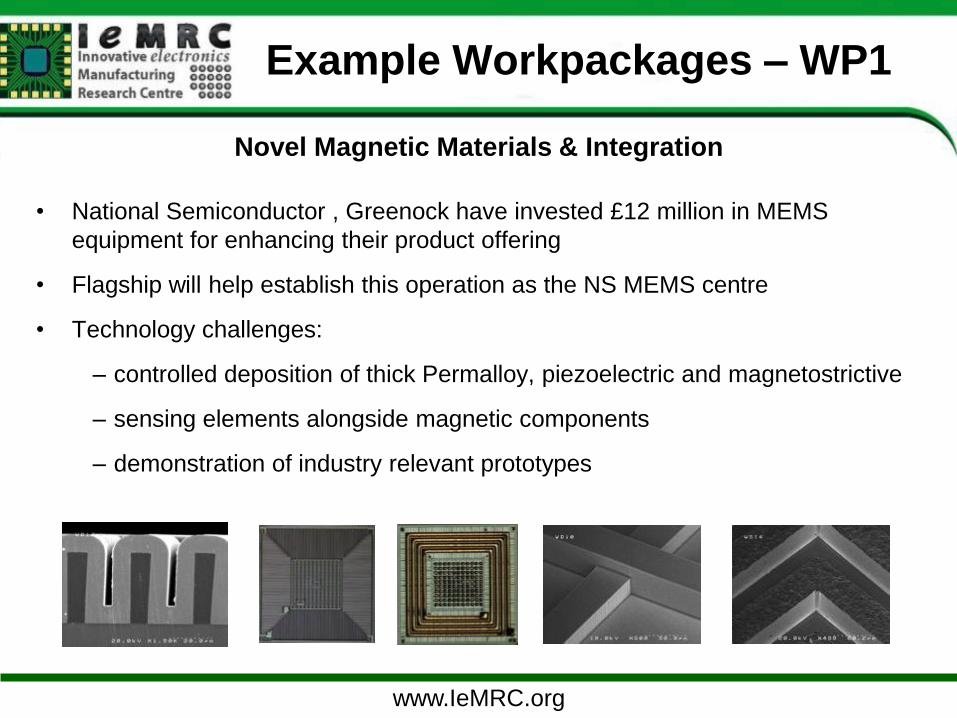
Example Workpackages – WP1
• National Semiconductor , Greenock have invested £12 million in MEMS
equipment for enhancing their product offering
• Flagship will help establish this operation as the NS MEMS centre
• Technology challenges:
– controlled deposition of thick Permalloy, piezoelectric and magnetostrictive
– sensing elements alongside magnetic components
– demonstration of industry relevant prototypes
Novel Magnetic Materials & Integration
www.IeMRC.org
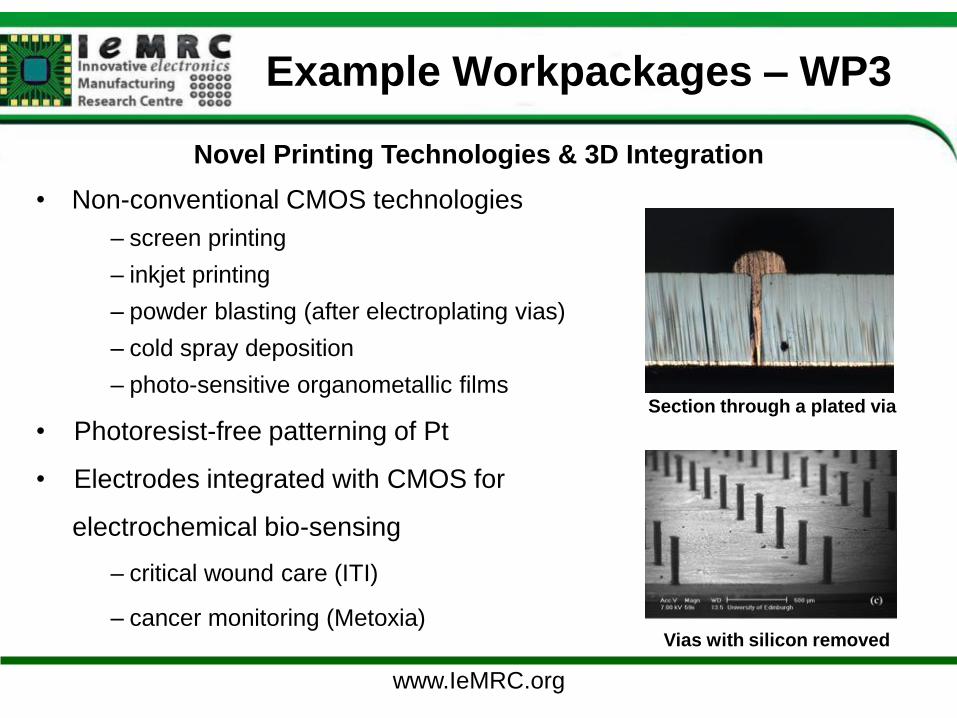
Example Workpackages – WP3
• Non-conventional CMOS technologies
– screen printing
– inkjet printing
– powder blasting (after electroplating vias)
– cold spray deposition
– photo-sensitive organometallic films
• Photoresist-free patterning of Pt
• Electrodes integrated with CMOS for
electrochemical bio-sensing
– critical wound care (ITI)
– cancer monitoring (Metoxia)
Novel Printing Technologies & 3D Integration
Section through a plated via
Vias with silicon removed
www.IeMRC.org
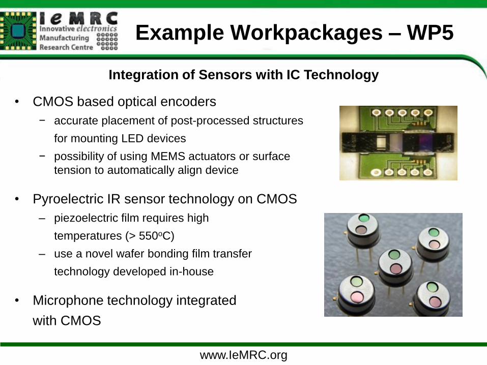
Example Workpackages – WP5
Integration of Sensors with IC Technology
• CMOS based optical encoders
− accurate placement of post-processed structures
for mounting LED devices
− possibility of using MEMS actuators or surface
tension to automatically align device
• Pyroelectric IR sensor technology on CMOS
– piezoelectric film requires high
temperatures (> 550oC)
– use a novel wafer bonding film transfer
technology developed in-house
• Microphone technology integrated
with CMOS
www.IeMRC.org
Summary
• The IeMRC is supporting electronics research in UK Universities
• This research aims to meet the needs of the UK electronics industry
• The IeMRC’s research includes work on printed & plastic electronics
• Printed electronics offers huge growth potential and has potential
applications in many new and exciting areas
• Also supporting a wide range of other research from silicon
processing to end of life and business issues.
www.IeMRC.org
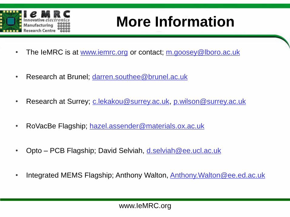
More Information
• The IeMRC is at www.iemrc.org or contact; [email protected]
• Research at Brunel; [email protected]
• Research at Surrey; [email protected], [email protected]
• RoVacBe Flagship; [email protected]
• Opto – PCB Flagship; David Selviah, [email protected]
• Integrated MEMS Flagship; Anthony Walton, [email protected]
www.IeMRC.org
The
Innovative Electronics Manufacturing
Research Centre (IeMRC)
www.IeMRC.org