Embed Size (px)
Citation preview

Printed Electronics and Offset LithographyInnovative Electronics Manufacturing SeminarElectronics Yorkshire June 26th 2007
Darren SoutheeDarren Southee(Gareth Hay, Peter Evans, David Harrison)(Gareth Hay, Peter Evans, David Harrison)The Cleaner Electronics Research Group,The Cleaner Electronics Research Group,
Brunel UniversityBrunel UniversityThe “Conductive Lithographic Film (CLF)” circuit fabrication process is a method of forming electronic circuit interconnect and components on flexible substrates via the offset lithographic printing process.

Overview
•• Conductive Lithographic Films (CLF) Conductive Lithographic Films (CLF) –– A short history 1995 A short history 1995 onwardsonwards
•• The power problemThe power problem•• Integrated printed electronic systems via the offset lithographiIntegrated printed electronic systems via the offset lithographic c
printing process?printing process?

CLF - A short history..•• Harrison, Harrison, BillettBillett & Billingsley began investigations into a circuit & Billingsley began investigations into a circuit
fabrication techniques for reduced environmental impact in 1996fabrication techniques for reduced environmental impact in 1996•• The process described involved the deposition of silverThe process described involved the deposition of silver--loaded loaded
conductive ink via offset lithographic printingconductive ink via offset lithographic printing•• It was envisaged that if successful this could vastly reduce theIt was envisaged that if successful this could vastly reduce the
environmental impact associated with the production of standard environmental impact associated with the production of standard PCBsPCBs
•• Offset had speed and material advantages over the alternative Offset had speed and material advantages over the alternative screen printingscreen printing
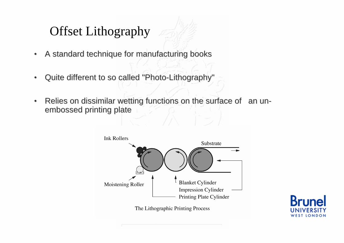
Offset Lithography
•• A standard technique for manufacturing books A standard technique for manufacturing books
•• Quite different to so called "PhotoQuite different to so called "Photo--Lithography" Lithography"
•• Relies on dissimilar wetting functions on the surface of an unRelies on dissimilar wetting functions on the surface of an un--embossed printing plateembossed printing plate
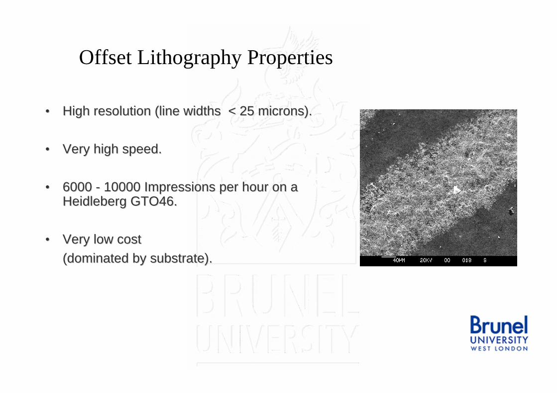
Offset Lithography Properties
•• High resolution (line widths < 25 microns).High resolution (line widths < 25 microns).
•• Very high speed. Very high speed.
•• 6000 6000 -- 10000 Impressions per hour on a 10000 Impressions per hour on a HeidlebergHeidleberg GTO46.GTO46.
•• Very low costVery low cost(dominated by substrate).(dominated by substrate).
Conductive Lithographic Films (CLF)Conductive Lithographic Films (CLF)
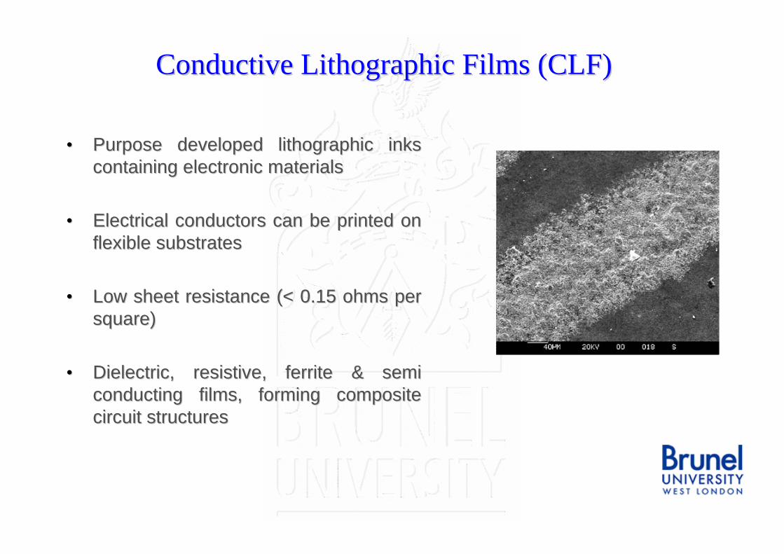
•• Purpose developed lithographic inks Purpose developed lithographic inks containing electronic materialscontaining electronic materials
•• Electrical conductors can be printed on Electrical conductors can be printed on flexible substratesflexible substrates
•• Low sheet resistance (< 0.15 ohms per Low sheet resistance (< 0.15 ohms per square)square)
•• Dielectric, resistive, ferrite & semi Dielectric, resistive, ferrite & semi conducting films, forming composite conducting films, forming composite circuit structurescircuit structures
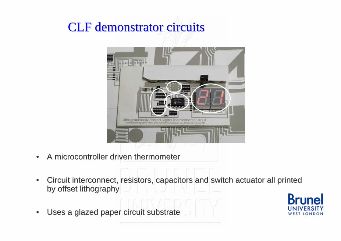
•• A microcontroller driven thermometerA microcontroller driven thermometer
•• Circuit interconnect, resistors, capacitors and switch actuator Circuit interconnect, resistors, capacitors and switch actuator all printed all printed by offset lithographyby offset lithography
•• Uses a glazed paper circuit substrateUses a glazed paper circuit substrate
CLF demonstrator circuitsCLF demonstrator circuits
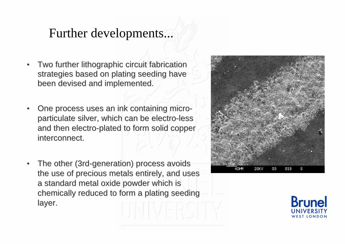
Further developments...
•• Two further lithographic circuit fabrication Two further lithographic circuit fabrication strategies based on plating seeding have strategies based on plating seeding have been devised and implemented.been devised and implemented.
•• One process uses an ink containing microOne process uses an ink containing micro--particulate silver, which can be electroparticulate silver, which can be electro--less less and then electroand then electro--plated to form solid copper plated to form solid copper interconnect.interconnect.
•• The other (3rdThe other (3rd--generation) process avoids generation) process avoids the use of precious metals entirely, and uses the use of precious metals entirely, and uses a standard metal oxide powder which is a standard metal oxide powder which is chemically reduced to form a plating seeding chemically reduced to form a plating seeding layer. layer.
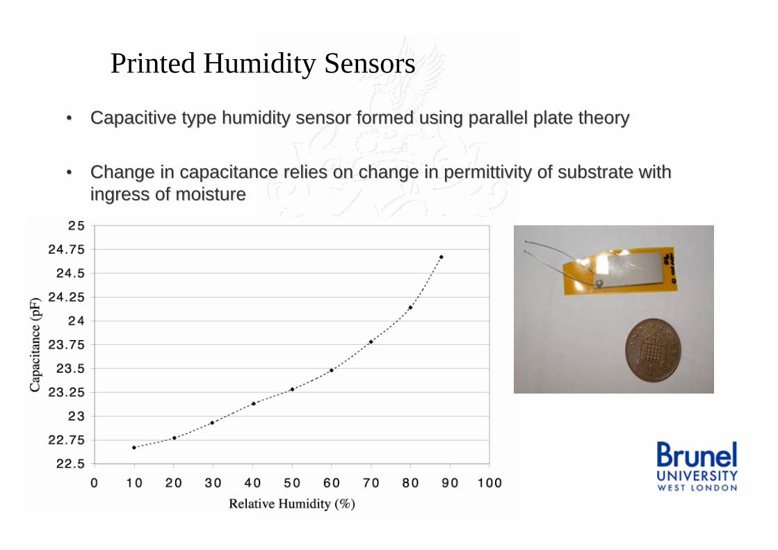
Printed Humidity Sensors
•• Capacitive type humidity sensor formed using parallel plate theoCapacitive type humidity sensor formed using parallel plate theoryry
•• Change in capacitance relies on change in permittivity of substrChange in capacitance relies on change in permittivity of substrate with ate with ingress of moistureingress of moisture
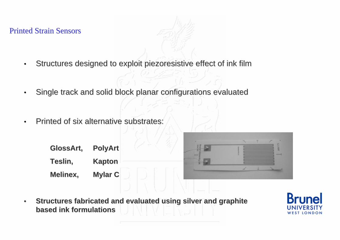
•• Structures designed to exploit piezoresistive effect of ink filmStructures designed to exploit piezoresistive effect of ink film
•• Single track and solid block planar configurations evaluatedSingle track and solid block planar configurations evaluated
•• Printed of six alternative substrates:Printed of six alternative substrates:
GlossArt, GlossArt, PolyArtPolyArt
Teslin, Teslin, KaptonKapton
Melinex,Melinex, Mylar CMylar C
•• Structures fabricated and evaluated using silver and graphite Structures fabricated and evaluated using silver and graphite based ink formulations based ink formulations
Printed Strain SensorsPrinted Strain Sensors
Strain Strain –– Resistance ResultsResistance Results
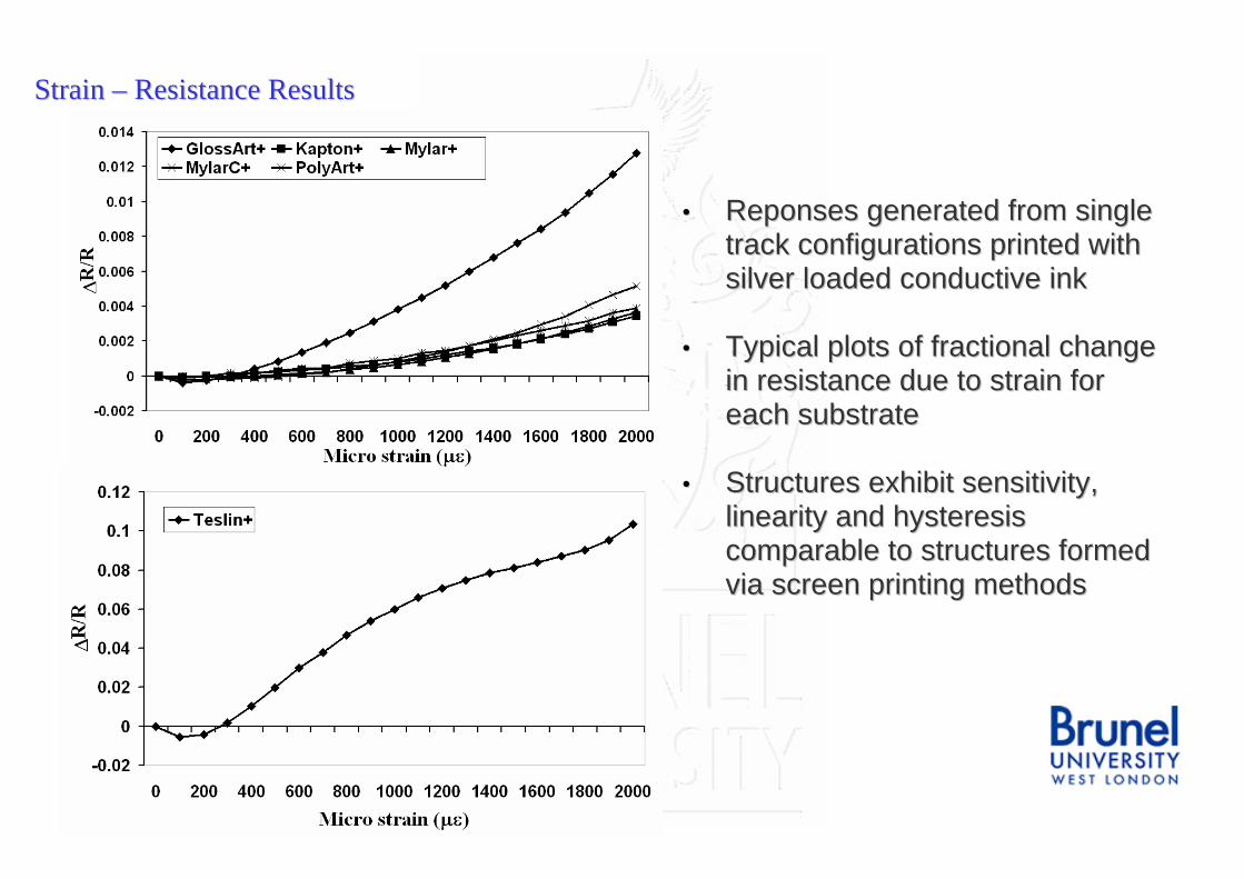
•• Reponses generated from single Reponses generated from single track configurations printed with track configurations printed with silver loaded conductive inksilver loaded conductive ink
•• Typical plots of fractional change Typical plots of fractional change in resistance due to strain for in resistance due to strain for each substrateeach substrate
•• Structures exhibit sensitivity, Structures exhibit sensitivity, linearity and hysteresis linearity and hysteresis comparable to structures formed comparable to structures formed via screen printing methodsvia screen printing methods
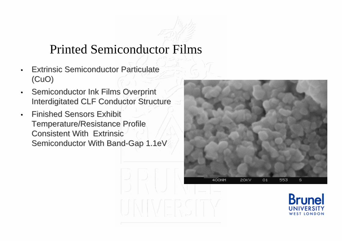
Printed Semiconductor Films•• Extrinsic Semiconductor Particulate Extrinsic Semiconductor Particulate
(CuO)(CuO)•• Semiconductor Ink Films Overprint Semiconductor Ink Films Overprint
Interdigitated CLF Conductor StructureInterdigitated CLF Conductor Structure•• Finished Sensors Exhibit Finished Sensors Exhibit
Temperature/Resistance Profile Temperature/Resistance Profile Consistent With Extrinsic Consistent With Extrinsic Semiconductor With BandSemiconductor With Band--Gap 1.1eV Gap 1.1eV
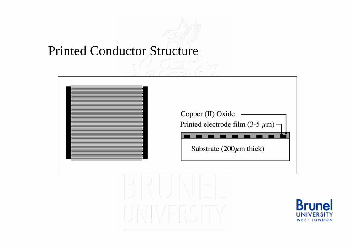
Printed Conductor Structure
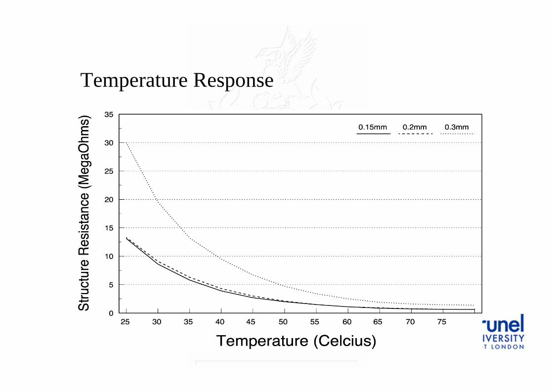
Temperature Response
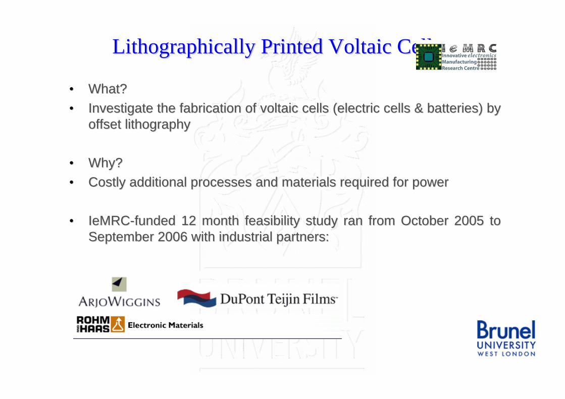
Lithographically Printed Voltaic CellsLithographically Printed Voltaic Cells
•• What?What?•• Investigate the fabrication of voltaic cells (electric cells & bInvestigate the fabrication of voltaic cells (electric cells & batteries) by atteries) by
offset lithographyoffset lithography
•• Why?Why?•• Costly additional processes and materials required for powerCostly additional processes and materials required for power
•• IeMRCIeMRC--funded 12 month feasibility study ran from October 2005 to funded 12 month feasibility study ran from October 2005 to September 2006 with industrial partners:September 2006 with industrial partners:

Initial workInitial work
•• Zinc Zinc –– Carbon Carbon ‘‘LeclancheLeclanche’’ chemistry chosenchemistry chosen
•• Initial cells fabricated to prove an electrochemical potential cInitial cells fabricated to prove an electrochemical potential could be ould be produced using CLF deposited inksproduced using CLF deposited inks
•• Two inks developed for anode and cathode electrode fabricationTwo inks developed for anode and cathode electrode fabrication
Zinc and Carbon:Zinc and Carbon:ParticulateParticulateResinResinSolventSolventAntiAnti--oxidantoxidant
Both inks displayed shear thinning and viscosity values Both inks displayed shear thinning and viscosity values around 7around 7--9 Pas at a shear rate of 400 9 Pas at a shear rate of 400 secsec--11
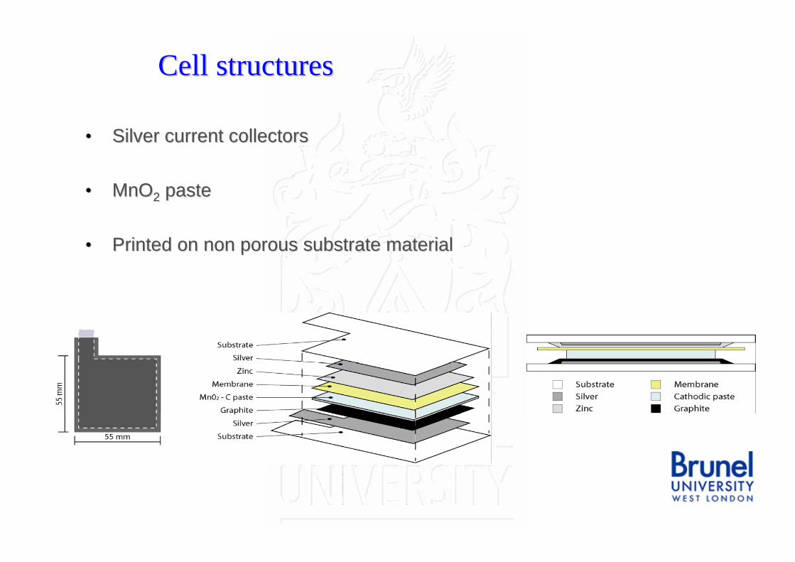
Cell structuresCell structures
•• Silver current collectorsSilver current collectors
•• MnOMnO22 pastepaste
•• Printed on non porous substrate materialPrinted on non porous substrate material

Cell internal resistanceCell internal resistance
••RaRa -- the resistance of the electrochemical path including the electrthe resistance of the electrochemical path including the electrolyte and the separatorolyte and the separator
••RmRm -- is the resistance of the metallic path through the cell includiis the resistance of the metallic path through the cell including the terminals, electrodes and interconnect ng the terminals, electrodes and interconnect
••CbCb -- the capacitance of the parallel plates which form the electrodethe capacitance of the parallel plates which form the electrodes of the cell. s of the cell.
••RiRi -- is the nonis the non--linear contact resistance between electrode and the electrolyte.linear contact resistance between electrode and the electrolyte.
••Simplified electrical circuitSimplified electrical circuit
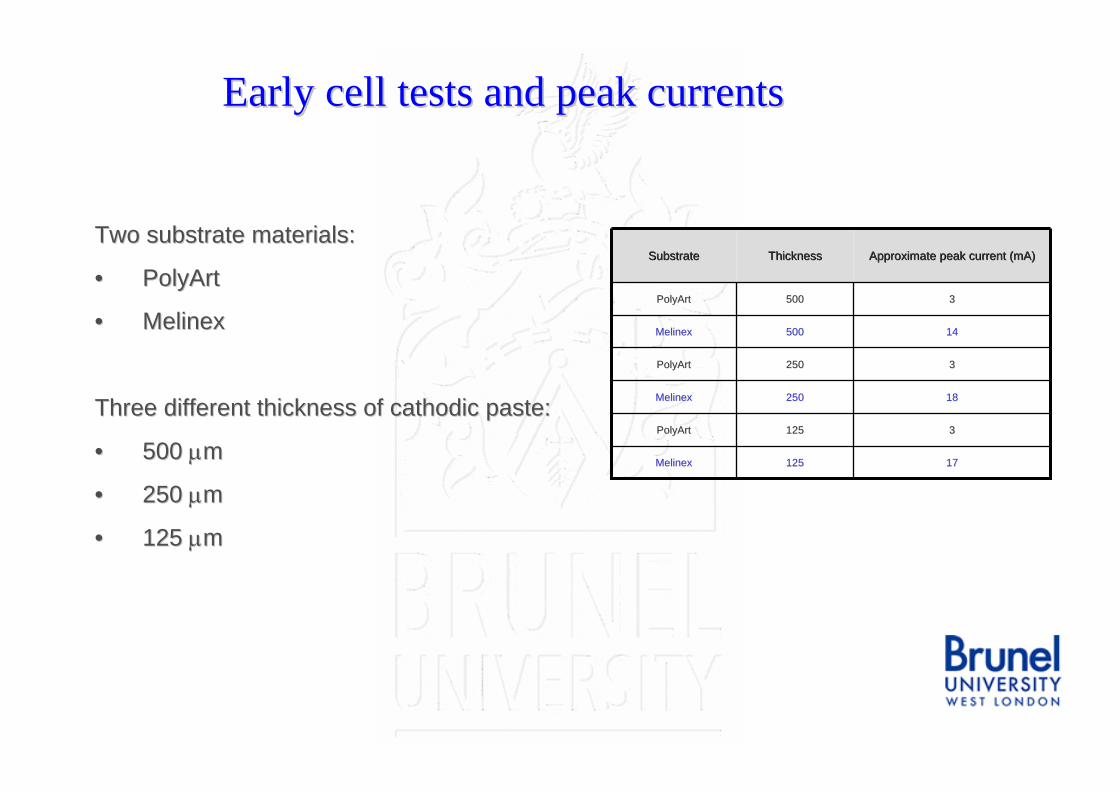
Early cell tests and peak currentsEarly cell tests and peak currents
Two substrate materials:Two substrate materials:
•• PolyArtPolyArt
•• MelinexMelinex
Three different thickness of Three different thickness of cathodiccathodic paste: paste:
•• 500 500 μμmm
•• 250 250 μμmm
•• 125 125 μμmm
1717125125MelinexMelinex
33125125PolyArtPolyArt
1818250250MelinexMelinex
33250250PolyArtPolyArt
1414500500MelinexMelinex
33500500PolyArtPolyArt
Approximate peak current (Approximate peak current (mAmA))ThicknessThicknessSubstrateSubstrate

Cell discharge curvesCell discharge curves
•• PolyArtPolyArt deposited electrodesdeposited electrodes
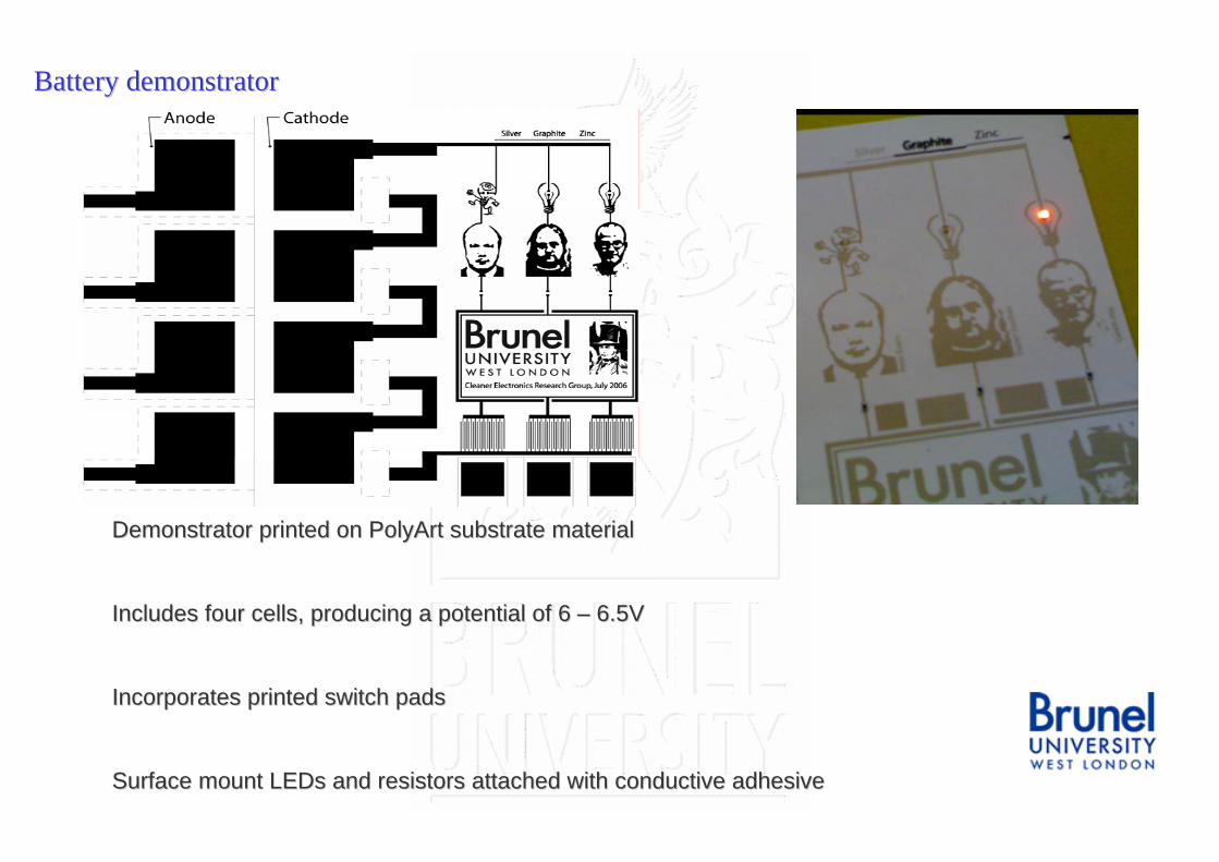
Battery demonstratorBattery demonstrator
Demonstrator printed on PolyArt substrate materialDemonstrator printed on PolyArt substrate material
Includes four cells, producing a potential of 6 Includes four cells, producing a potential of 6 –– 6.5V6.5V
Incorporates printed switch padsIncorporates printed switch pads
Surface mount Surface mount LEDsLEDs and resistors attached with conductive adhesiveand resistors attached with conductive adhesive
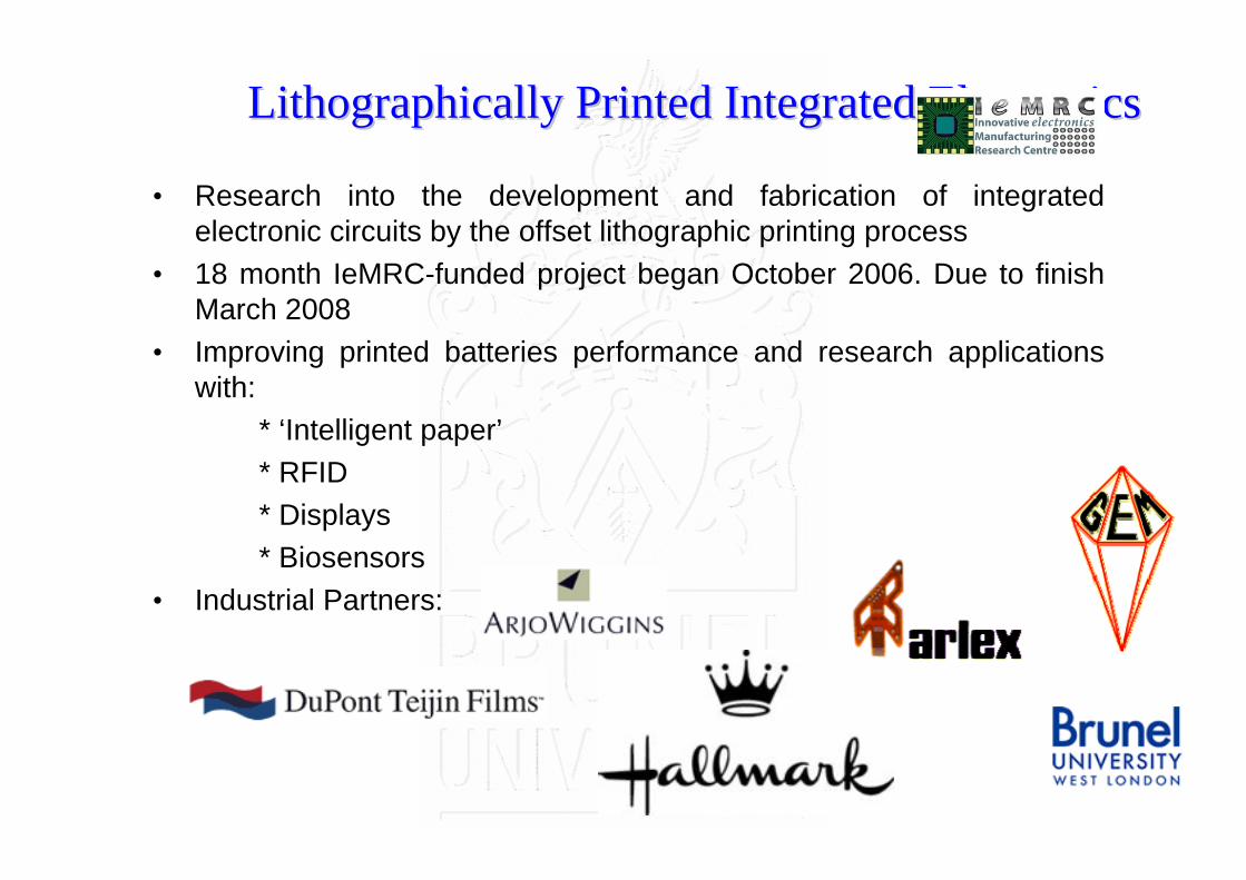
Lithographically Printed Integrated ElectronicsLithographically Printed Integrated Electronics
• Research into the development and fabrication of integrated electronic circuits by the offset lithographic printing process
• 18 month IeMRC-funded project began October 2006. Due to finish March 2008
• Improving printed batteries performance and research applications with:
* ‘Intelligent paper’* RFID* Displays* Biosensors
• Industrial Partners:
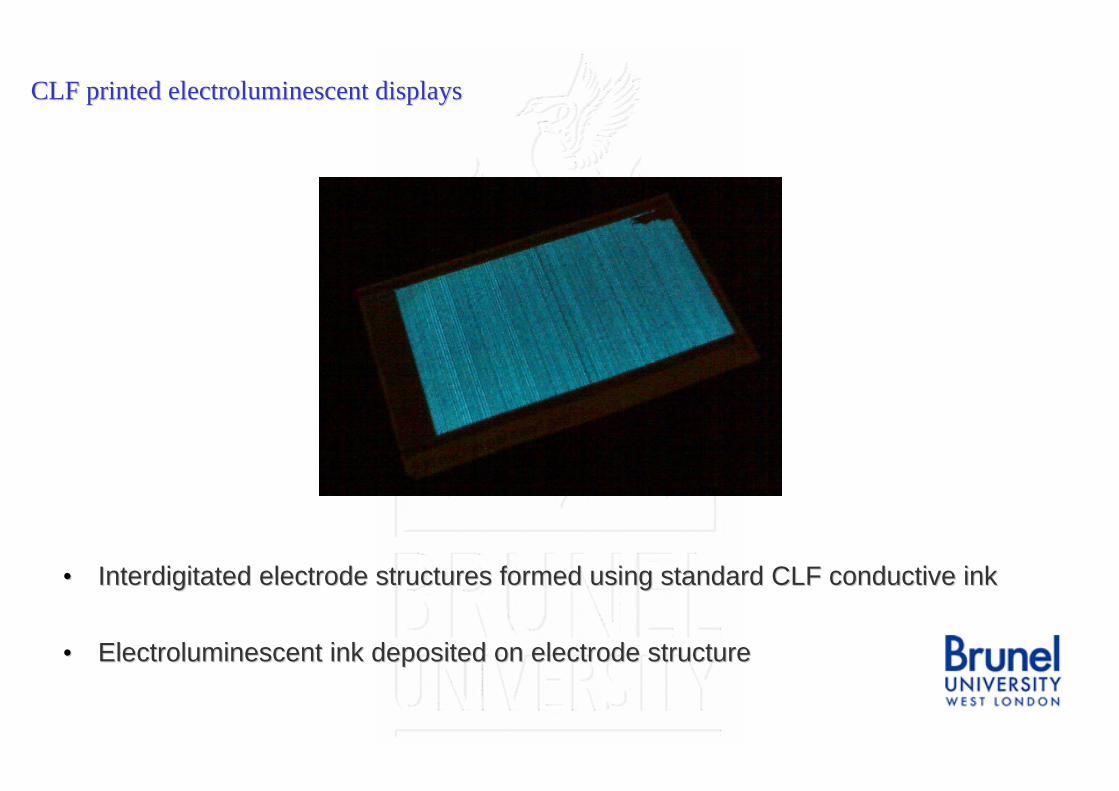
CLF printed electroluminescent displaysCLF printed electroluminescent displays
•• InterdigitatedInterdigitated electrode structures formed using standard CLF conductive inkelectrode structures formed using standard CLF conductive ink
•• Electroluminescent ink deposited on electrode structureElectroluminescent ink deposited on electrode structure
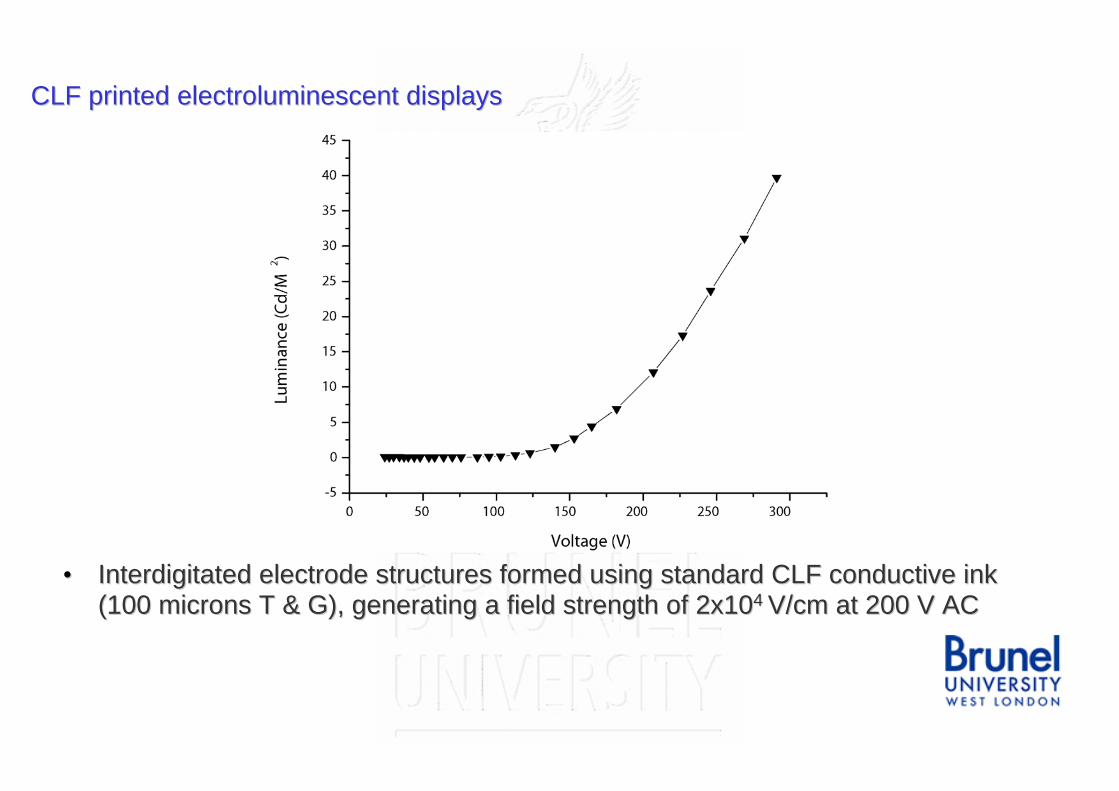
CLF printed electroluminescent displaysCLF printed electroluminescent displays
•• InterdigitatedInterdigitated electrode structures formed using standard CLF conductive ink electrode structures formed using standard CLF conductive ink (100 microns T & G), generating a field strength of 2x10(100 microns T & G), generating a field strength of 2x10⁴ 4 V/cm at 200 V ACV/cm at 200 V AC

CLF displaysCLF displays
•• CLF printed CLF printed thermochromicthermochromicdisplaydisplay
•• Heating elements printed using Heating elements printed using resistive inkresistive ink
•• ThermochromicThermochromic ink deposited ink deposited aboveabove

Lithographically Printed Integrated ElectronicsLithographically Printed Integrated Electronics
•• ProgressProgressVoltaic cells developed with improved performanceVoltaic cells developed with improved performanceInitial work on integrated systems carried outInitial work on integrated systems carried outOther chemistries investigatedOther chemistries investigatedElectrochemical Impedance Spectroscopy (EIS) analysis of cells Electrochemical Impedance Spectroscopy (EIS) analysis of cells

Darren Southeespent eight years working in the electronics industry in service, production and design roles. He designed the TD201 Digital Storage Adapter for THANDAR Electronics Ltd (1987) and the TA320 Logic Analyser for TTi Ltd (1992). His academic career has included roles at Bournemouth University – researching non-invasive blood sugar measurement, Bradford University (UAE) and the University of Lincoln. He is currently Course Director for the undergraduate programme in Industrial Design & Technology at Brunel University and a member of the Cleaner Electronics Research Group. He has been an investigator on grants awarded by the EU, EPSRC and PARK.Darren’s primary research over the past four years has been the development of printed power sources and he has been PI on two IeMRC (EPSRC) grants in this area. Recent research outputs include two patents and four journal publications in printed electronics.He is a member of the IET and a Fellow of the Higher Education Academy