Embed Size (px)
Citation preview

Master of Science Thesis in Electrical EngineeringDepartment of Electrical Engineering, Linköping University, 2020
Power Supply Rejection (PSR)Enhancement Techniques for FullyIntegrated Low-Dropout (LDO)Regulators
Saptarshi Banerjee

Master of Science Thesis in Electrical EngineeringDepartment of Electrical Engineering, Linköping University, 2020
Förbättring av stabilströmförsörjning med heltintegreradeLow-Dropout-Regulatorer (LDO)
Saptarshi Banerjee
Linköpings UniversitetSE–581 83 Linköping
+46 13 28 10 00, www.liu.se

UpphovsrättDetta dokument hålls tillgängligt på Internet - eller dess framtida ersättare - under 25 år frånpubliceringsdatum under förutsättning att inga extraordinära omständigheter uppstår.
Tillgång till dokumentet innebär tillstånd för var och en att läsa, ladda ner, skriva ut enstaka kopiorför enskilt bruk och att använda det oförändrat för ickekommersiell forskning och för undervisning.Överföring av upphovsrätten vid en senare tidpunkt kan inte upphäva detta tillstånd. All annananvändning av dokumentet kräver upphovsmannens medgivande. För att garantera äktheten,säkerheten och tillgängligheten finns lösningar av teknisk och administrativ art.
Upphovsmannens ideella rätt innefattar rätt att bli nämnd som upphovsman i den omfattningsom god sed kräver vid användning av dokumentet på ovan beskrivna sätt samt skydd mot attdokumentet ändras eller presenteras i sådan form eller i sådant sammanhang som är kränkandeför upphovsmannens litterära eller konstnärliga anseende eller egenart.
För ytterligare information om Linköping University Electronic Press se förlagets hemsida:http://www.ep.liu.se/.
CopyrightThe publishers will keep this document online on the Internet - or its possible replacement - for aperiod of 25 years starting from the date of publication barring exceptional circumstances.
The online availability of the document implies permanent permission for anyone to read, todownload, or to print out single copies for his/hers own use and to use it unchanged for non-commercial research and educational purpose. Subsequent transfers of copyright cannot revokethis permission. All other uses of the document are conditional upon the consent of the copyrightowner. The publisher has taken technical and administrative measures to assure authenticity,security and accessibility.
According to intellectual property law the author has the right to be mentioned when his/her workis accessed as described above and to be protected against infringement.
For additional information about the Linköping University Electronic Press and its proceduresfor publication and for assurance of document integrity, please refer to its www home page:http://www.ep.liu.se/.
© Banerjee

Master of Science Thesis in Electrical EngineeringPower Supply Rejection (PSR) Enhancement Techniques for Fully
Integrated Low-Dropout (LDO) RegulatorsSaptarshi Banerjee
LiTH-ISY-EX–20/5352–SE
Supervisors:Prakash Harikumar
Ericsson, Linköping, SwedenMark Vesterbacka
ISY, Linköping University
Examiner:Ted Johansson
ISY, Linköping University
Division of Integrated Circuits and SystemsDepartment of Electrical Engineering
SE-581 83 Linköping, Sweden©2020 Saptarshi Banerjee

AbstractIn this present world, there is a huge requirement of portable devices for that theanalysis of low-dropout or LDO regulators have been on high priority. So, for everyrespective device, there is a power budget that acts as the main constraint to designan LDO. The LDO design aims to suppress the noise and supply noise-free or lownoise output.This thesis paper illustrates several designs of output capacitor-less LDO architec-ture to enhance Power Supply Rejection (PSR) and optimization of the ideas fromdifferent literature to achieve the low quiescent current, stability with fast transientresponse while the input voltage is low over a wide range of load current. Differ-ent types of transistor schematic designs under definite specifications of the LDOs,which are mostly integrated by major components like Error Amplifier (EA) andpass transistor, feedback resistors, and relatively small output capacitor have mostlyconsidered for the designs. However, some buffer attenuation techniques which canimprove the PSR have also been shown with proper diagram. The design of LDOwith the components and how to design the pass device and their trade off’s havebeen has been discussed. Different techniques of PSR enhancement among whichsome of the techniques have been implemented have been illustrated with respectivediagrams. A study of executed techniques under the specifications with comparativeresults has been shown with their trade-off with the other architecture.The contribution is an LDO that has been simulated in Cadence spectre and designedin CMOS FinFET process node at Vdd = 0.95 V with a load current of 50 mA -75 mA and an output voltage of 0.75 V with a small output capacitor of 200 pF, aPSR of −25 dB at 100 MHz has been achieved whereas the current consumption atthe load is 245 µA, while meeting the targeted stability analysis of gain margin andphase margin of 47 dB and 63 respectively. A small voltage droop of 36. 6mV forrising edge and −15.99 mV for falling edge over a 100 µA to 75 mA step change in10 ns has been observed.
Keywords: LDO, PSR, Output Pole, Load Current, EA, FVF, SF, ESSF, SSF,PVT, FOM
i

SammanfattningI dagens värld finns det stora behov av bärbara enheter och krav på analys avregulatorer (LDO). För varje typ av enhet finns det en energibudget som fungerarsom huvudsaklig begränsning för att utforma en LDO. LDO-konstruktion syftar tillatt leverera brusfri eller lågbrusig utspänning. Detta examensarbete visar på flerakonstruktioner av utgångskondensatorfria LDO-arkitekturer för att förbättra PowerSupply Rejection (PSR). Optimering av idéer från olika litteraturkällor görs för attuppnå låg viloström och stabilitet med snabb respons med låg ingångsspänning överett brett intervall av lastström.Olika typer av konstruktioner schemanivå för precisa LDO-specifikationer, mestadelsintegrerade med de viktigaste komponenter såsom felförstärkare (Error Amplifier,EA) och passtransistor, återkopplingsmotstånd och relativt små utgångskonden-satorer, har studerats. Buffertdämpningstekniker som kan förbättra PSR har ocksåinkluderats. Konstruktion av LDO:er på komponentnivå och man utformar pass-enheten och dess kompromisser diskuteras också. Implementering av några olikatekniker för PSR-förbättring illustreras med schema. En studie av utförda teknikerenligt specifikationerna med jämförande resultat ingår också.Resultat är en LDO som har simulerats i Cadence Spectre i en CMOS FinFETprocess med en matningsspänning på 0,95 V, en belastningsström på 50 mA - 75mA, en utspänning på 0,75 V och med en liten utgångskondensator på 200 pF. PSRpå −25 dB vid 100 MHz har uppnåtts medan strömförbrukningen vid belastningenär 245 µA, samtidigt som kraven på marginal för förstärkning på 47 dB och fas 63°har uppnåtts. Ett litet spänningsfall på 36,6 mV för stigande signal och −15,99mV för fallande signal under en förändring från 100 µA till 75 mA på 10 ns harobserverats.
Keywords: LDO, PSR, Output Pole, Load Current, EA, FVF, SF, ESSF, SSF,PVT, FOM
ii

AcknowledgementsI am very grateful to those who have helped me along in this ambitious journey.
• My grandmother N. Goswami for her selfless love, support andunwavering belief in me.
• My mother K. Banerjee for ingraining in me tenacity, that has helpedpersevere throughout my master studies. Her boundless love and supporthelped me prevail.
• My aunt D. Chakraborty, uncle S. Chakrabortty and my cousin S.Chakrabortty who made it possible for me to pursue my Masters Degree.I am very thankful to them for their unconditional love and support.
• My supervisor P. Harikumar, who took it upon himself to teach me theins and outs of the work. He has pushed me to not only to get my workdone on my topic, but to also explore and gain knowledge on analogdesign. He taught me how to approach and present my work in atechnical way. He has guided me with tailoring my report. I am verygrateful for the support and knowledge he provided during meetings andfor patiently answering all my questions. He has always emboldened meto think in my own way, while encouraging me to test the boundaries ofcurrent limitations. His valuable feedback on the design architectures andon this scientific documentation elevated the quality of my work. He hasinspired me to be the very best version of my professional self.
• My reporting manager R. Hägglund, who gave me the opportunity towork at Ericsson with his team of talented and enthusiastic engineers. Hegave me a life changing opportunity to work with the esteemed R&D RFData Converter Design department to work on my thesis. I will be forevergrateful for the times he spared to impart technical knowledge to me whileat work. He guided me while at work to keep my focus. I am thankful tohave been afforded the opportunity to call R. Hägglund, my mentor.
• My supervisor Prof. Mark Vesterbacka from Linköping University whohelped me solve my queries regarding the manuscript.
• I would sincerely like to thank my examiner Prof. Ted Johansson whohelped me from the beginning of this thesis work and with all the tasksassociated with the formal procedure. His guidance was key to solvingadministrative difficulties that arose and had the potential to prolong thetimeline.
• Lastly, I want to thank all of my close friends who made my journeynotable at Linköping University.
Saptarshi Banerjee, Linköping, August 2020
iii

AcronymsPSR Power Supply RejectionPSRR Power Supply Ripple RejectionLDO Low-DropoutFOM Figure Of MeritOCL Output Capacitor-LessEA Error AmplifierSRC Supply Ripple CancellationASRC Adaptive Supply Ripple CancellationBRI Body Ripple InjectorBIA Buffer Impedance AttenuationSTC Single Transistor ControlSF Source FollowerSSF Super Source FollowerESSF Enhanced Super Source FollowerPVT Process Voltage TemperatureFVF Flipped Voltage FollowerESR Equivalent Series ResistanceLGS Loop Gain StabilizationUGF Unity Gain FrequencyGBW Gain Bandwidth ProductVCVS Voltage Control Voltage SourceVCCS Voltage Control Current SourcePCB Printed Circuit BoardBJT Bipolar Junction TransistorPMOS Positive Channel Metal-Oxide SemiconductorNMOS Negative Channel Metal-Oxide Semiconductor
iv

Contents
Abstract i
Sammanfattning ii
Acknowledgements iii
Acronyms iv
1 Introduction 11.1 Motivation . . . . . . . . . . . . . . . . . . . . . . . . . . . . . . . . . 11.2 Aim . . . . . . . . . . . . . . . . . . . . . . . . . . . . . . . . . . . . 11.3 Research questions . . . . . . . . . . . . . . . . . . . . . . . . . . . . 11.4 Methodology and Delimitations . . . . . . . . . . . . . . . . . . . . . 21.5 Thesis Structure . . . . . . . . . . . . . . . . . . . . . . . . . . . . . . 2
2 Overview of Regulators 42.1 Overview of LDO . . . . . . . . . . . . . . . . . . . . . . . . . . . . . 42.2 Specification of LDO . . . . . . . . . . . . . . . . . . . . . . . . . . . 6
2.2.1 DC Electrical Characteristics . . . . . . . . . . . . . . . . . . 62.2.1.1 Input Voltage Range and Line Regulation . . . . . . 62.2.1.2 Dropout Voltage . . . . . . . . . . . . . . . . . . . . 62.2.1.3 Quiescent Current . . . . . . . . . . . . . . . . . . . 62.2.1.4 Load Regulation and Output Accuracy . . . . . . . . 62.2.1.5 Power Dissipation . . . . . . . . . . . . . . . . . . . 7
2.2.2 AC Specification . . . . . . . . . . . . . . . . . . . . . . . . . 72.2.2.1 Transient Line Response . . . . . . . . . . . . . . . . 72.2.2.2 Transient Load Response . . . . . . . . . . . . . . . 72.2.2.3 PSR . . . . . . . . . . . . . . . . . . . . . . . . . . . 72.2.2.4 Output Noise . . . . . . . . . . . . . . . . . . . . . . 8
2.2.3 Conversion Efficiency . . . . . . . . . . . . . . . . . . . . . . . 82.2.4 Figure Of Merit (FOM) . . . . . . . . . . . . . . . . . . . . . 8
3 Design of Low-dropout Regulators 93.1 Choice of Pass Transistor . . . . . . . . . . . . . . . . . . . . . . . . . 93.2 Classification of LDO Regulator . . . . . . . . . . . . . . . . . . . . . 103.3 Analog LDO . . . . . . . . . . . . . . . . . . . . . . . . . . . . . . . . 10
3.3.1 Off-Chip Load Capacitor Based LDO . . . . . . . . . . . . . . 113.3.1.1 Dominant Pole Compensation Technique . . . . . . . 11
3.3.2 Off-Chip Load Capacitor Less LDO . . . . . . . . . . . . . . . 123.3.2.1 Traditional Pass-Transistor Output Stage . . . . . . 12
v

CONTENTS CONTENTS
3.3.2.2 FVF Output Stage . . . . . . . . . . . . . . . . . . . 133.3.2.2.1 Dominant Pole at LDO Output Node . . . . 133.3.2.2.2 Dominant Pole at Output of Error Amplifier 13
3.4 Digital LDO . . . . . . . . . . . . . . . . . . . . . . . . . . . . . . . . 15
4 Analysis of Finite PSR in LDOs 164.1 Power Supply Rejection Ratio . . . . . . . . . . . . . . . . . . . . . . 164.2 PSR Limitations of Conventional LDO . . . . . . . . . . . . . . . . . 17
5 PSR Enhancing Techniques 205.1 Increasing Bandwidth . . . . . . . . . . . . . . . . . . . . . . . . . . . 205.2 Flipped Voltage Follower . . . . . . . . . . . . . . . . . . . . . . . . . 205.3 Interposing Buffer Stage . . . . . . . . . . . . . . . . . . . . . . . . . 21
5.3.1 Super Source Follower . . . . . . . . . . . . . . . . . . . . . . 225.3.2 Enhanced Super Source Follower . . . . . . . . . . . . . . . . 23
5.4 Loop Gain Stabilization . . . . . . . . . . . . . . . . . . . . . . . . . 235.5 Supply Ripple Cancellation . . . . . . . . . . . . . . . . . . . . . . . 24
6 Method 266.1 Design Specification . . . . . . . . . . . . . . . . . . . . . . . . . . . . 266.2 Implementation . . . . . . . . . . . . . . . . . . . . . . . . . . . . . . 26
6.2.1 Conventional LDO . . . . . . . . . . . . . . . . . . . . . . . . 266.2.2 LDO With Improved Bandwidth . . . . . . . . . . . . . . . . 276.2.3 LDO With Interposed Buffer Stage . . . . . . . . . . . . . . . 276.2.4 Variants of FVF-LDO . . . . . . . . . . . . . . . . . . . . . . 27
6.2.4.1 FVF-LDO with Output Dominated Pole . . . . . . . 286.2.4.2 FVF-LDO with Internal Dominant Pole . . . . . . . 29
6.3 Evaluation . . . . . . . . . . . . . . . . . . . . . . . . . . . . . . . . . 30
7 Results 317.1 Implementation . . . . . . . . . . . . . . . . . . . . . . . . . . . . . . 31
7.1.1 Conventional LDO . . . . . . . . . . . . . . . . . . . . . . . . 317.1.2 LDO with Improved Bandwidth . . . . . . . . . . . . . . . . . 337.1.3 LDO with Interposed Buffer Stage . . . . . . . . . . . . . . . 357.1.4 Variants of FVF-LDO . . . . . . . . . . . . . . . . . . . . . . 37
7.1.4.1 FVF-LDO with Output Dominant Pole . . . . . . . . 377.1.4.2 FVF-LDO with Internal Dominant Pole . . . . . . . 38
7.2 Evaluation . . . . . . . . . . . . . . . . . . . . . . . . . . . . . . . . . 40
8 Discussion 418.1 Results . . . . . . . . . . . . . . . . . . . . . . . . . . . . . . . . . . . 418.2 Method . . . . . . . . . . . . . . . . . . . . . . . . . . . . . . . . . . 41
9 Conclusion and Future Work 439.1 Conclusion . . . . . . . . . . . . . . . . . . . . . . . . . . . . . . . . . 439.2 Future Work . . . . . . . . . . . . . . . . . . . . . . . . . . . . . . . . 43References . . . . . . . . . . . . . . . . . . . . . . . . . . . . . . . . . . . . 45
vi

List of Figures
2.1 LDO Block Diagram . . . . . . . . . . . . . . . . . . . . . . . . . . . 42.2 Conventional LDO Schematic Diagram . . . . . . . . . . . . . . . . . 5
3.1 Types of BJT Pass Transistor Configuration [1] . . . . . . . . . . . . 93.2 Types of CMOS Pass Transistor Configuration [1] . . . . . . . . . . . 103.3 LDO Design Structure . . . . . . . . . . . . . . . . . . . . . . . . . . 103.4 LDO with Dominant Pole at Output [1] . . . . . . . . . . . . . . . . 113.5 LDO with Miller Compensation Technique [1] . . . . . . . . . . . . . 133.6 FVF-LDO with Dominant Pole at Output Node [2] . . . . . . . . . . 143.7 FVF-SSF LDO with Dominant Pole at Output of EA [3] . . . . . . . 143.8 Basic Schematic of Digital LDO [4] . . . . . . . . . . . . . . . . . . . 15
4.1 PSR Plot of Conventional LDO . . . . . . . . . . . . . . . . . . . . . 174.2 Supply Ripple Coupling Paths of LDO [5] . . . . . . . . . . . . . . . 184.3 Floating and Grounded Capacitors with VCCS [5] . . . . . . . . . . . 18
5.1 Increasing Bandwidth with Conventional LDO . . . . . . . . . . . . . 205.2 (a) FVF Circuit [6] (b) FVF based LDO [7] . . . . . . . . . . . . . . 215.3 (a) Intermediate buffered LDO [8] (b) Conventional Source Follower [8] 225.4 Enhanced-Super Source Follower LDO . . . . . . . . . . . . . . . . . 235.5 Loop-Gain Stabilization Architecture [9] . . . . . . . . . . . . . . . . 245.6 (a) Gate Injection SRC [10]; (b) Body Injection SRC [10] . . . . . . . 255.7 Adaptive Supply Ripple Cancellation Technique Architecture [10] . . 25
6.1 Conventional LDO Architecture . . . . . . . . . . . . . . . . . . . . . 266.2 LDO with Interposed Buffer Stage . . . . . . . . . . . . . . . . . . . . 276.3 (a) Source Follower; (b) Super Source Follower; (c) Enhanced Super
Source Follower . . . . . . . . . . . . . . . . . . . . . . . . . . . . . . 286.4 Output Curve of SF, SSF, ESSF . . . . . . . . . . . . . . . . . . . . . 286.5 Implemented FVF-LDO with Output Dominated Pole . . . . . . . . . 296.6 FVF-LDO with Internal Dominant Pole . . . . . . . . . . . . . . . . 30
7.1 PSR Plot of Conventional LDO . . . . . . . . . . . . . . . . . . . . . 317.2 Transient Response of Conventional LDO . . . . . . . . . . . . . . . . 327.3 Transient Response Over PVT Corner of Conventional LDO . . . . . 327.4 PSR Plot of LDO with Improved Bandwidth . . . . . . . . . . . . . . 337.5 Transient Response Over Nominal Corner of LDO with Improved
bandwidth . . . . . . . . . . . . . . . . . . . . . . . . . . . . . . . . . 337.6 Transient Response Over PVT Corner of LDO with Improved band-
width . . . . . . . . . . . . . . . . . . . . . . . . . . . . . . . . . . . . 34
vii
LIST OF FIGURES LIST OF FIGURES
7.7 PSR Plot LDO with Interposed Buffer Stage . . . . . . . . . . . . . . 357.8 Transient Response Over Nominal Corner of LDO with Interposed
Buffer Stage . . . . . . . . . . . . . . . . . . . . . . . . . . . . . . . . 367.9 Transient Response Over PVT Corner of LDO with Interposed Buffer
Stage . . . . . . . . . . . . . . . . . . . . . . . . . . . . . . . . . . . . 367.10 PSR Plot of FVF-LDO with Output Dominant Pole . . . . . . . . . . 377.11 Transient Response of FVF-LDO with Output Dominant Pole . . . . 377.12 PSR Plot of FVF-LDO with Internal Dominant Pole . . . . . . . . . 387.13 Transient Response Over Nominal Corner of FVF-LDO with Internal
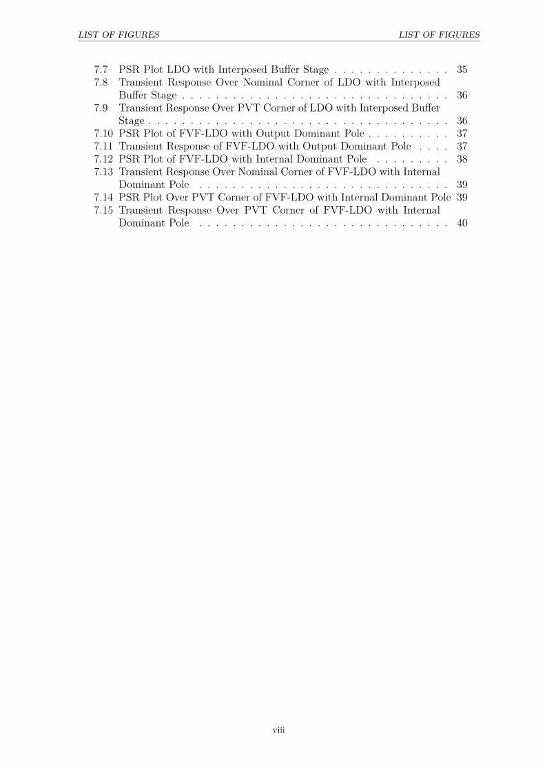
Dominant Pole . . . . . . . . . . . . . . . . . . . . . . . . . . . . . . 397.14 PSR Plot Over PVT Corner of FVF-LDO with Internal Dominant Pole 397.15 Transient Response Over PVT Corner of FVF-LDO with Internal
Dominant Pole . . . . . . . . . . . . . . . . . . . . . . . . . . . . . . 40
viii

List of Tables
7.1 Results from Conventional LDO . . . . . . . . . . . . . . . . . . . . . 337.2 Results from LDO with Improved Bandwidth . . . . . . . . . . . . . 347.3 Results from LDO with Interposed Buffer Stage . . . . . . . . . . . . 357.4 Results from FVF-LDO with Internal Dominant Pole . . . . . . . . . 387.5 Results from FVF-LDO with Internal Dominant Pole (Fast Loop) . . 387.6 Table of Comparison of All Techniques . . . . . . . . . . . . . . . . . 40
i

1Introduction
In this chapter, the motivation and the aim of this thesis has been discussed in thefirst two sections. In section 1.3 some research questions have been asked based oncurrent research and study on LDOs. In the last section, a small description of eachchapter has been discussed.
1.1 MotivationThe high demand for portable devices like mobile phones, laptops make it appro-priate to design low- dropout or LDO regulators although low-dropout regulatorsare also being used in automotive industries. So, portable devices that require lowquiescent current and low voltage make the battery life longer with improved ef-ficiency. To decrease the battery cells and reduce the cost while using the simpledesign structure LDOs are being designed. LDO which is a form of linear regulatorworks effectively at low voltage without degrading the performance of the device.The dc-dc converters can be used in place of LDOs but they are costly. This thesisis based on the enhancement of power supply rejection techniques in LDOs whichmeans to supply optimum power at the analog or digital block without any largevariation at the input supply voltage.
1.2 AimThe aim of this thesis is to testify different techniques with their advantages andtrade offs to achieve the wide-band power supply rejection of capacitor-less low-dropout regulators. Some techniques have been modified to reach more accuratevalue of power supply rejection with respect to the expected specifications.
1.3 Research questionsThe Thesis is based on below two important research questions:1. Evaluate various LDO architecture in literature to identify suitable candidate
for achieving high PSR over wide bandwidth.2. Design on transistor schematic level an output capacitor-less LDO, targeting
PSR of less than or equal to −25 dB at 100 MHz. LDO should achieve stability,transient response with a small on chip load capacitor 100 pF - 200 pF. LDOshould support low voltage operation where input voltage is 0.95 V providingoutput voltage of 0.75 V to the load circuits.
1

1.4. METHODOLOGY AND DELIMITATIONS Chapter 1
1.4 Methodology and DelimitationsThe adopted methodology follows a literature survey to understand the basic LDOcircuit and to design an appropriate LDO block and state-of-art performance. Onthe basis of the specifications given, the different circuits blocks have been modeled.Also combining different techniques from publications and modified them from theconventional structure also been applied to optimize the design. The simulationscomprehensively include process corners, supply voltage variation and temperaturescale.This thesis work broadly lack of a connection with ethical and societal aspects.As the portable device and battery efficient device might have connection with theethical and societal aspect but LDO as on own is a small circuit inside an SoC devicewhich alone can not affect much in these aspects.
1.5 Thesis StructureThis thesis work is mainly focused on designing the architecture to meet the speci-fications of wide-band PSR of output capacitor-less LDO. Designing the LDO withfast transient response using different topologies from the literature was part of thedelimitation of this thesis work too.As from the structural contents of this paper, this paper has been divided into six (2to 7) main chapters from discussing the basics of LDO to design the LDO and withthe specifications for this thesis work to get wide-band PSR LDO and ends with thediscussion chapter where all the benefits and trade offs of the different implementedarchitecture has been discussed.Chapter 2 is the introduction to the LDO block and its different parameters. A briefdescription has been given with the block diagram as well as the schematics of theLDO to make the reader understand the contribution of the LDO block in an SoCdevice. In the section 2.2 the specifications of the LDO has been divided in AC andDC characteristics to make it more specific regarding important parameters.Chapter 3 discusses the design of the LDO with its classification. The design ofpass device introduces the chapter. While after that LDO classification takes moredetailed discussion, but in this thesis work analog LDO has been prioritize more asthe LDO designed is analog LDO. Some detailed description about analog LDO andits types has also been described with some schematic representation. Lastly thischapter concludes by digital LDO and its trade off over analog LDO.Chapter 4 is describing the supply ripple coupling of finite PSR in LDOs. Thischapter starts with small introduction of PSR and how it looks as graphically forconventional LDOs. But the main focus is to discuss the limitations of PSR inconventional LDO. The contribution of each part from the conventional LDO ar-chitecture has been described. The different supply ripple coupling paths with theproper equations have been shown with schematics example.Enhancing the power supply rejection or PSR with different architectures has beendescribed briefly with respective schematics in chapter 5. A conventional LDO ar-chitecture has been chosen to increase the bandwidth and then other techniqueslike flipped voltage follower and interposing buffer stage have also been describedbriefly. Two of the techniques, loop gain stabilization and supply ripple cancel-
PSR Enh. Tech. for Fully Int. LDOs 2 Saptarshi Banerjee

1.5. THESIS STRUCTURE Chapter 1
lation techniques has been described though it has not been implemented in thiswork.The concepts from chapter 5 has been taken and improved to implement the differentarchitectures to meet the specifications which described in method or chapter 6.There are five techniques has been implemented among which four techniques canfollow the input specifications whereas FVF-LDO with ideal buffer has been opt outas the it is not suitable for the load current with respect to design flow.Chapter 7 is the mirror image of chapter 6 as the sub headings are kept same tomake the reader understand and connect between two chapters, where the resultsof the implemented methods have been showed graphically and in tabular form.Different simulations like nominal, PVT and transient response have been shownhere with respected to different architecture.In the chapter 8 the discussion about the results and their comparative studies havebeen described. In the method section all the methods have been compared withrespect to design parameter and expected results and which one suits best for thisthesis work. The research question which has been asked in chapter 1 has also beendiscussed in this chapter.Chapter 9 brings the conclusion of the research. It has also some future workrecommendation for further studies in this domain.
PSR Enh. Tech. for Fully Int. LDOs 3 Saptarshi Banerjee

2Overview of Regulators
This Chapter gives a general introduction to fundamentals of LDO and its perfor-mance metrics and a basic introduction to topologies and terminologies of LDO.Also the Concept of Power Supply Rejection (PSR) enhancement techniques ofLDO.
2.1 Overview of LDO
Low-dropout (LDO) regulator is a circuit that provides ripple-free voltage to theanalog/RF blocks of a device and the input to output voltage difference is very lowin these certain circuits. Figure 2.1, describes the block level diagram of LDO [11].In any electronic device, a battery will supply the input voltage (which is always fedby the battery charger) and there will be a switching converter, which will regulatethe output voltage to drive the rest of the circuit. Switching converters increased theripple frequency, with the increasing bandwidth of LDO as new wireless networkshave a high sample rate of ADC and clock rate which will affect analog/RF blocks.This will degrade the whole performance of the chip. So, an LDO regulator which isalso known as a linear regulator is placed after the switching converter to eliminatethe ripple in the supply voltage. So, LDOs are designed to work at a high bandwidthwith a good power supply rejection value to mitigate this problem. So that it canprovide a ripple free supply voltage to the input of the analog/RF block. In thenext half of this section an LDO schematic has been shown and voltage regulationis described.
Figure 2.1: LDO Block Diagram
4

2.1. OVERVIEW OF LDO Chapter 2
In order to discuss further in conventional LDO regulators a large off-chip capacitoris placed in order to make the whole system stable. But now-a-days smaller analogdevices and processors forcing the research interest to have a smaller off-chip ca-pacitor for an LDO regulator. This will be good for chip integration process. Thesmall off-chip load capacitor can be the reason for many issues like slow transientresponse and stability degradation. An important constraint of LDO regulator ispower supply rejection or PSR, which measures the LDO’s ability to reduce theoutput voltage ripple caused by the noise introduced in the input voltage. This willbe a new challenge to improve the PSR if the LDO is off-chip load capacitor-less.Though, different techniques like pole splitting is using for off-chip capacitor-lessLDO to make the regulation stable [12].A schematic diagram of an conventional LDO has been illustrated in figure 2.2 [13].In the figure an Error Amplifier (EA), two feedback resistors R1 and R2, a outputcapacitor Cout and a pass transistor can be observed, which are the main designelements of LDO regulator. The reference voltage or Vref can be provided by thereference block as shown in the Figure. The pass device can be PMOS or NMOSwhere the input voltage is applied. In this thesis PMOS is used as a pass transistor.The reason of choosing PMOS over NMOS is discussed in next chapter in section3.1. The error amplifier will compare the output voltage Vout with the referencevoltage Vref provided by reference block. From the figure the output of the erroramplifier is connected to the gate of the pass transistor, now the gate voltage iscontrolled by the fluctuation of Vout. Although the feedback loop maintained thestability of the output voltage [12].
Figure 2.2: Conventional LDO Schematic Diagram
PSR Enh. Tech. for Fully Int. LDOs 5 Saptarshi Banerjee

2.2. SPECIFICATION OF LDO Chapter 2
2.2 Specification of LDOIn this section some parameters and design variable is discussed to design a LDO[14]. This section is divided into DC electrical characteristics, AC specifications,PSR, output noise and stability consideration of LDO regulator.
2.2.1 DC Electrical CharacteristicsHere are the dc electrical characteristics is described. In this section parameterslike input voltage range, dropout voltage, quiescent current, load regulation, outputaccuracy and power dissipation is described.
2.2.1.1 Input Voltage Range and Line Regulation
To design an LDO regulator, this parameter act as one of the important parameter.The range of allowable input voltage at the power supply input of the LDO is calledthe input voltage range [14]. But one more parameter is related to input voltagerange, that is line regulation, Lr. Line regulation is the ability of the power supplyto maintain the specified output voltage even if the input line voltage changes. Ifthe input voltage difference is ∆Vi and output voltage difference is ∆Vo then,
Lr = ∆Vo
∆Vi
(2.1)
2.2.1.2 Dropout Voltage
This is also another important parameter to design an LDO. The smallest voltagedifference between regulator’s input and output voltage, which will maintain the out-put voltage regulation is called dropout voltage [15]. This is inversely proportionalto the power efficiency. The dropout voltage should be small for high performanceLDO. Lets, assume dropout voltage as VDo and where Vi is input voltage and Vo isoutput voltage then,
VDO = Vi − V0 (2.2)
2.2.1.3 Quiescent Current
Current efficiency is depends on quiescent current. So, that also resembles thebattery life of the device. quiescent current also known as ground current, is thedifference between input and output currents when the load is very low. PMOSsare better for their low IQ as they are voltage driven. The quiescent current has theapproximately same value with the load current so, when the load current is lowIQ become the main factor of battery life [15]. If the quiescent current is IQ then,
IQ = Ii − I0 (2.3)
2.2.1.4 Load Regulation and Output Accuracy
Load regulation is the ability of the power supply to maintain its specified outputvoltage given changes in load current [16]. When the output current varies frommaximum to zero or zero to maximum rated value, then the worst case of theoutput voltage variation happens [15]. If ∆Vo is output voltage variation, ∆Io is
PSR Enh. Tech. for Fully Int. LDOs 6 Saptarshi Banerjee

2.2. SPECIFICATION OF LDO Chapter 2
load current variation, if Ro−reg is load regulation then [16],
Ro−reg = ∆Vo
∆Io
(2.4)
So, load regulation measures the drive capability of LDO when there are changes inoutput load current [14]. But in correspondence to measure accuracy it includes lineregulation, load regulation, reference voltage and temperature coefficient [15].
2.2.1.5 Power Dissipation
In any power related device temperature is considered as main factor as it can causeserious casualty of the device. So to allow the maximum junction temperaturewithout damaging the device LDOs have been specified with the definite junctiontemperature for normal operations [14] [15]. This constraint limits the power dissi-pation of LDO. In order to evaluate LDO regulator’s power dissipation, PD [15],let assume input voltage Vi, output voltage Vo and output current Io then [15],
PD = (Vi − V0) ∗ Io (2.5)
But the maximum allowable power dissipation (PDm) is dependent on junction tem-perature (TJ). The maximum power dissipation might be equal or more than thepower dissipation of the LDO [11]. To measure the junction temperature, if the am-bient temperature is TA and thermal resistance junction to ambient for that deviceis RT then [14],
TJ = TA + (PDm ∗RT ) (2.6)
2.2.2 AC SpecificationHere the ac analysis of LDO is explained. Some important specifications like lineresponse, load response, PSR are more likely to be focused in this section.
2.2.2.1 Transient Line Response
If a step change of input voltage is applied at the input of LDO, then the outputvoltage has to be change for different input voltages [15]. This is a steady-stateparameter. Line regulation is proportional to the open loop gain. The outputvoltage variation is supposed to be the value of line response. In chapter 6 thereare methods tried of different techniques with their transient response has beenillustrated.
2.2.2.2 Transient Load Response
As the line response, load response is also a steady-state parameter. Load currenttransition results in the variation of output voltage. If the open loop gain valueincreased then the load regulation will also be increased [15].
2.2.2.3 PSR
Power Supply Rejection or PSR is the key parameter of LDO design. PSRor power supply rejection evaluates the variation of the output voltage for a givenchange on the input. As in the equation 2.7, Vo is the response at the LDO outputnode due to the noise/ripple injected on the Vi node. Technically the output shouldbe independent from the variations on the input but for practical aspects there willbe some limitations in this case [14]. So at higher bandwidth like 100 MHz the
PSR Enh. Tech. for Fully Int. LDOs 7 Saptarshi Banerjee

2.2. SPECIFICATION OF LDO Chapter 2
rejection will be zero or very less because of the contribution of control loop. So aloop compensation is needed for the output voltage to be stable [14]. This is alsodepends on analysis of poles and zeros. PSR can be improved by using large outputcapacitor and low equivalent series resistance [15].
PSR = 20log(Vo−ripple
Vi−ripple
) (2.7)
2.2.2.4 Output Noise
Output noise is generated when a scale of different frequencies is applied whilethe load current is constant and the input voltage is ripple free [15]. So, the outputnoise is dependent on closed loop gain of the LDO and noise of the input stage of theerror amplifier [14]. A noise at the error amplifier input will amplify and resultanta noise signal can be observed at the LDO output.
2.2.3 Conversion EfficiencyPower efficiency is necessary for LDO regulators and should be high as per theirapplications. The efficiency can measured as,
Efficiency = IoVo
(Io + IQ)Vi
100 (2.8)
to achieve a high efficiency the quiescent current and dropout voltage should beless [15]. It can be affected by the input/output factor or power dissipation as thedifference between input and output voltage should be small. At voltage and largeload current the quiescent current effect can be neglected whereas the efficiencycan be measured by the switching converter. But with a small load current, thequiescent can effect the maximum efficiency. So, current efficiency should be highin order to get improve battery performance, but transient response, stability andbandwidth can be degraded for low quiescent current [17].
2.2.4 Figure Of Merit (FOM)Figure Of Merit or FOM is a measurement used to characterize the performanceof an electronic device. To calculate the FOM, there are some certain formulasanalysed in [18] and [19]. If the response time is TR, quiescent current is IQ, voltagedifference at output ∆Vo and Imax is the load current then FOM1 can be measuredby [18],
FOM1 = TRIQ
Imax
= C ∗∆Vout
Imax
∗ IQ
Imax
(2.9)
FOM1 can be measured by nano-second or ns. The regulator will be efficient if theFOM value is small. A disadvantage of FOM1 in replica bias source follower is thatdroop and current efficiency can not be adopted by desired numbers. So, a newhas been designed which can help to eradicate some quantity of process dependency[18]. The other FOM2 used for this work analysed from [19].
FOM2 = K∆VoIQ
∆Iout
(2.10)
where, K is edge time ratio measured in terms of volts.
K = ∆t used in the measurementthe smallest ∆t from the designs of comparison
(2.11)
PSR Enh. Tech. for Fully Int. LDOs 8 Saptarshi Banerjee

3Design of Low-dropout Regulators
This chapter describes the design and the elements to design of regulators. In section3.2, a brief discussion on classification of LDO is illustrated.
3.1 Choice of Pass TransistorIn an LDO regulator pass transistor act as a switch or tap to regulate the outputvoltage. The type of pass transistor should be determined carefully to design anLDO regulator. In order to design the pass transistor with BJTs like NPN Darling-ton, NPN, PNP can be referred to get high driving capability as BJTs have highcurrent gain [1]. BJTs have two disadvantages which are the large drop out voltage
Figure 3.1: Types of BJT Pass Transistor Configuration [1]
and large leakage current at the base terminal [1]. In Darlington and NPN configu-ration the dropout voltage is relatively large than PNP configuration. But in PNPconfiguration dropout voltage is lower than the other two types of BJT pass device.The large voltage dropout is caused by base-emitter and collector-emitter’s voltagedrop to work BJT in active region. Other disadvantage is large leakage current inbase terminal as the base current is proportional to the ratio of collector currentand the current gain of PNP and NPN transistor [1]. But PNP is the efficient con-figuration but it has large leakage current due to low current gain where PNP hashigh current gain [1].
In the Figure 3.2 types of configuration with CMOS have been illustrated. So foravoiding the disadvantages of the BJTs the CMOS logic is being used for LDOregulators. Though MOSFET has a small driving capability than BTJ, to overcome
9

3.2. CLASSIFICATION OF LDO REGULATOR Chapter 3
Figure 3.2: Types of CMOS Pass Transistor Configuration [1]
that a large aspect ratio is required for MOSFETs. For low-dropout voltage andquiescent current PMOS is the only solution to design LDO. But PMOS takes largersilicon area as it has lower mobility for the holes [1]. But NMOS works as a sourcefollower stage which is functioning as buffer in LDO. So a large voltage drop-outcan be notified which is a drawback of NMOS. A charge pump shown in the figurecan be used to decrease the dropout voltage.
3.2 Classification of LDO RegulatorLDO regulators can be broadly classified into analog LDOs and digital LDOs. Asillustrated in Figure 3.3 [1]. The classification of analog LDO has been describedwith respect to output load capacitor and different pole compensation techniques,although off-chip load capacitor-less LDO is the targeted area of work for this thesis.A highlight on FVF stage at the output with the pole location is described. Alsoa small introduction of digital LDO is included with the disadvantages over analogLDO is discussed at the section 3.4.
Figure 3.3: LDO Design Structure
3.3 Analog LDOAnalog LDO can be classified in off-chip load capacitor based and off-chip loadcapacitor less LDO. A large off chip capacitor is used in off-chip load capacitor based
PSR Enh. Tech. for Fully Int. LDOs 10 Saptarshi Banerjee

3.3. ANALOG LDO Chapter 3
LDO to make the dominant pole at the output node of the LDO. Whereas in off-chip load capacitor less LDO has some different compensation techniques like Millercompensation and flipped voltage follower which have been described in followingsections.
3.3.1 Off-Chip Load Capacitor Based LDOIn this section a dominant pole compensation technique has been enforced accordingto the location of the dominant pole. In dominant pole compensation technique witha large off chip load capacitor, the dominant pole can be formed at the output nodeof LDO or at the gate of the pass transistor. But a large off-chip capacitor takesmore PCB area, which is a disadvantage of this class of LDO.
3.3.1.1 Dominant Pole Compensation Technique
In the Figure 3.4, a large capacitor is installed to form the dominant pole at theoutput node of the LDO [1], which can be named as dominant pole compensation.As shown in the Figure 3.4, LDO contains an error amplifier (EA), a pass device
Figure 3.4: LDO with Dominant Pole at Output [1]
Mp and two feedback divider resistor R1 and R2. Here a large capacitor (Cgd)is present at gate to drain terminal of PMOS pass transistor. To calculate theparasitic capacitance (Cpar) at the gate, Cgd and the voltage gain of PMOS shouldbe determined. So the first low frequency non-dominant pole is located at the gateof the PMOS pass device.
P1 = 1roa ∗ Cpar
(3.1)
So, roa, the output resistance of error amplifier is very high to maintain the lowquiescent current. The dominant pole compensation technique includes an outputimpedance network which consists two capacitors, one is large output capacitor
PSR Enh. Tech. for Fully Int. LDOs 11 Saptarshi Banerjee

3.3. ANALOG LDO Chapter 3
Cout and other one is bypass capacitor Cb. Considering the ESR of Cout for stabilityanalysis because Cb is smaller than Cout [1]. So, the two poles contributed by Cout
and Cb are,Po = 1
rout ∗ Cout
(3.2)
Load current act important role on frequency response, if load current increasesthe dominant pole Po shifts to high frequencies [1] as shown in the equation below,
Po = 1rout ∗ Cout
∝ Iload (3.3)
As the load current increases the loop gain Lo decreases, but the unity gain frequency(UGF) will also shifts towards high frequencies because Po is also moving towardshigher frequencies but this will degrade the performance of the LDO so this willlead to stability limitations.
UGF = Lo ∗ Po ∝√Iload (3.4)
So, when the UGF shifts to high frequencies, phase margin will decrease with theincreasing load. Aiming for stability consideration in different load condition withvariable UGF is challenging in ESR compensation skill. But using a large ESR canmitigate this issue by creating a zero.
3.3.2 Off-Chip Load Capacitor Less LDOIn the section 3.3.1.1 dominant pole compensation technique has been illustrated byusing large on-chip capacitor to locate the dominant pole at the output node of theLDO. But now-a-days in integrated LDOs, capacitor-less LDO reduce bonding wiresand takes less silicon area to connect with off-chip blocks [1]. In some conventionaltechniques Miller compensation can be used to form the dominant pole at the outputby using a small Miller circuit which also helps to increase the stability of the system.But a convenient compensation technique without using large on-chip capacitor thedominant pole has been located at the output node of the LDO by interposing a lowimpedance buffer stage between error amplifier and power stage of the LDO whereflipped voltage follower topology has been implemented at the output stage.
3.3.2.1 Traditional Pass-Transistor Output Stage
In this technique the dominant pole has been formed at the gate node of the passtransistor of the off-chip load capacitor-less LDO. An example of the schematics hasbeen showed in the Figure 3.5 [1]. The LDO consists of an error amplifier with singleMiller compensation with Miller capacitor Cm. If we consider the error amplifierstage then it has a transconductance for its differential pairs to provide the highgain, whereas the pass transistor will involve with the output impedance. Millercapacitance will form the dominant pole at the output node of the error amplifierat the low frequencies [1].
PSR Enh. Tech. for Fully Int. LDOs 12 Saptarshi Banerjee

3.3. ANALOG LDO Chapter 3
Figure 3.5: LDO with Miller Compensation Technique [1]
3.3.2.2 FVF Output Stage
As described above flipped voltage follower stage is at the output stage of the off-chip load capacitor less LDO, where two different type of topology can be classifiedwith the respect of the dominant pole location. The dominant pole can be placedat the output node of the LDO or at the output node of the error amplifier.
3.3.2.2.1 Dominant Pole at LDO Output NodeIn the Figure 3.6 simple schematic of flipped voltage follower based LDO has beenillustrated where the dominant pole is located at the output node. The schematic isbased on three different circuits which are error amplifier, Vset generation stage andflipped voltage follower stage consecutively. In this schematic the current I2 and I3and size of the transistors M7 and M8 are equal. The main priority of this structureis to keep the regulation same throughout all the nodes from Vout to Vref . HereVmir=Vref where Vmir is controlled by error amplifier. And Vset is generated fromVmir which is controlled by diode connectedM7. At the flipped voltage follower nodeVout is set by Vset. This is the process of regulating the Vref in all the nodes. Thereare low frequency poles which are Pout and Pgate [2]. A large on chip capacitor canbe used for the large load current but that will make the system unstable if Pout isdominant pole. So, a buffer stage is added with low output impedance to mitigatethe problem. The buffer stage is used (triangle shaped in the diagram) to the gateof the pass device which helps to push the two poles Pgate and Pout at the higherfrequencies [2]. This will locate the Pout as the dominant pole at the output nodeof the LDO.
3.3.2.2.2 Dominant Pole at Output of Error AmplifierThe another classification where the dominant pole is located at the output of theerror amplifier by adding a large decoupling capacitor. In the Figure 3.7, a schematichas been illustrated which is structured with flipped voltage follower with a supersource follower as a low impedance buffer stage. The flipped voltage follower is
PSR Enh. Tech. for Fully Int. LDOs 13 Saptarshi Banerjee

3.3. ANALOG LDO Chapter 3
Figure 3.6: FVF-LDO with Dominant Pole at Output Node [2]
Figure 3.7: FVF-SSF LDO with Dominant Pole at Output of EA [3]
formed with Mp, the pass transistor and Q2 is the common-gate amplifier. Thecurrent I1 defines the quiescent current of Q2. To make the output pole as dominant
PSR Enh. Tech. for Fully Int. LDOs 14 Saptarshi Banerjee

3.4. DIGITAL LDO Chapter 3
pole a large capacitor has to choose. In this topology there are two loop one is slowloop and another one is fast loop. If slow loop is being considered from Vout to erroramplifier to maintain a good dc accuracy, a large decoupling capacitor is added tothe gate of Q2 to get a clean node with respect to the ground [3]. This capacitorwill form a dominant pole at the gate of the Q2 in lower frequency than the polesin the fast loop. So, it will help the loop to stabilize faster [3].
3.4 Digital LDOFigure 3.8 illustrates the basic schematic of digital LDO regulator, consist of acomparator, control unit (consist of a bidirectional shift register), a power MOSFETarray and an output capacitor Cout. The comparator compares the voltage differencebetween Vout and Vref , then it output the control signal to control unit, then a power
Figure 3.8: Basic Schematic of Digital LDO [4]
PMOS will be turn on or off to modulate the Vout close to Vref [4]. The transientspeed is limited as one of the PMOS can be turn on or off in each clock cycle forshift register to operate. This is the one disadvantages of digital LDO over analogLDO as transient speed depends on clock frequency [4].But there are some disadvantages of digital LDO over analog LDO and vice versa,with respect to design constraints. In many cases analog LDO has low currentefficiency as the quiescent current is high [20]. But compare to digital LDO thecurrent efficiency is high due to low quiescent current in comparator and controller.Although some drawbacks which may be cause issues in digital LDO, are slow tran-sient response and large output ripple. A low clock frequency can be the reasonfor small quiescent current, but with slow transient response. So, to increase thetransient response a high clock frequency needed, which cause stability problem andsteady-state limit cycle oscillation [4].
PSR Enh. Tech. for Fully Int. LDOs 15 Saptarshi Banerjee

4Analysis of Finite PSR in LDOs
4.1 Power Supply Rejection RatioIn this section the limitations regarding supply ripple coupling of the PSR is dis-cussed. The location of the poles, open-loop gain, UGF and gain bandwidth productor GBW can affect PSR. LDO regulator depends on the location of poles and zerosof the feedback loop in order to stable the system.Power supply rejection or PSR is a very important parameter as it measures theripple rejection of a circuit from an input power supply over various frequencies.PSR can be measured by comparing the output ripple and input ripple [21] in 4.1.
PSR = 20logRippleoutput
Rippleinput
(4.1)
But PSR can also be measured by taking the ratio of open-loop gain of regulatorfeedback loop and the gain from Vin to Vout. So, by increasing open-loop gain PSRcan be increased. Another parameter can affect the PSR is transient response asPSR is specified at definite frequencies [21]. So, improving PSR can improve thetransient response and vice-versa [21]. As open-loop gain is one of the deciding factorof high PSR, so LDO must have high gain with high unity gain frequency. which canmake the loop unstable [21]. From the PSR analysis in [21], PSR performance can bedivided into three different regions, the first region at low frequencies, is dominatedby DC open-loop gain and bandgap PSR, the second region at mid frequencies,where PSR is dominated by open-loop gain to UGF which is dominated by erroramplifier bandwidth and the third region at high frequencies above UGF wherefeedback loop are neglected [21] [22]. A graphical representation has been shownbelow in Figure 4.1 for better understanding the behaviour of PSR.
16

4.2. PSR LIMITATIONS OF CONVENTIONAL LDO Chapter 4
Figure 4.1: PSR Plot of Conventional LDO
4.2 PSR Limitations of Conventional LDOThere are some PSR limitations in LDO at high frequencies due to different pathsbetween noise supply and output. In the Figure 4.2, there are three different pathshave been shown, where the first path is noise modulation of gate voltage throughCgs, which converted to current by transconductance of the pass transistor gmp;second path can be observed through the error amplifier and third path through thefinite output impedance of the pass transistor RdsP and Cdb. The output voltagecan be measured by below equation [5]
Vout = 11 + LoopGain(s) ∗ ((id−Cgs(s) + id−EA(s) + id−Rdsp+Cdb(s))Zload) (4.2)
Here from the equation the noise induced by the path 1, path 2 and path 3 isid−Cgs(s), id−EA(s) and id−Rdsp+Cdb(s) respectively. The supply ripple noise can becancelled by increasing the loop gain, though the stability can be sacrificed. Thereare different PSR limitations due to gate-source capacitance of pass transistor, erroramplifier and the pass transistor output impedance [5] discussed below.The pass transistor limits the LDOs PSR as the gate voltage is modulated by supplyvoltage through gate source capacitance. The voltage difference between source andgate of the pass transistor determine the drain current at the output of the LDO.Cgd creates local feedback which makes Vgate a function of output voltage. The gatedrain capacitor in the Figure 4.3 has four components two grounded capacitors andtwo voltage control current source. The voltage control current source is sCgdVout
is a local feedback. The gate source capacitor is also divided into two pieces but donot effect the analysis. The gate voltage voltage equation can be measured from [5]
PSR Enh. Tech. for Fully Int. LDOs 17 Saptarshi Banerjee

4.2. PSR LIMITATIONS OF CONVENTIONAL LDO Chapter 4
Figure 4.2: Supply Ripple Coupling Paths of LDO [5]
Vgate = [ sCgs1
Rg+ sCG
]Vdd = (Cgs
CG
)Vdd = ( Cgs
Cp + Cgs + Cgd
)Vdd (4.3)
In the above equation Cp can be ignored as Mp is bigger so Cgs and Cgd is biggerthan Cp.
Figure 4.3: Floating and Grounded Capacitors with VCCS [5]
PSR Enh. Tech. for Fully Int. LDOs 18 Saptarshi Banerjee

4.2. PSR LIMITATIONS OF CONVENTIONAL LDO Chapter 4
As mostly single ended amplifiers have been used in the LDOs which can has a lim-ited common mode and supply noise rejection. Single ended amplifier configurationcurrent is not equally divided into two arms due to transistor mismatch at the dif-ferential pair, which generates differential current at output [5]. On the other handimpedance at the source of the differential pair transistor is not same as the load isdifferent for different transistor. So optimization of LDOs performance on the basisof post layout simulation is needed to reduce the impact of the issues. If transistormismatches reduced, there can be some noise from Vdd. Hence the differential tosingle-ended conversion leads to limited power supply. The second stage will alsoinclude noise at Vgate which is cited and measured in [5].At high frequencies the Vgate is determined by Cgs or path 1, where the path 2 isnegligible. So, the noise for path 1 and path 2 can be measured by [5],
id−Cgs+EA = gmp(Vdd − Vgate) + sCgdVgate
= gmp( Cgd + Cp
Cgs + Cgd + Cp
)Vdd + sCgd( Cgs
Cgs + Cgd + Cp
)Vdd (4.4)
Here (Cgd +Cp) is controlling the leakage of Vdd noise at medium and high frequen-cies. It is hard to design the value of (Cgd + Cp), in order to get robust PSR atdifferent load conditions [5].The last limiting factor of LDOs PSR is Rds or path 3. The supply ripple noise canbe measured as [5],
id−Rdsp = ( 1Rdsp
+ sCdb)Vdd (4.5)
As the zero formed at higher frequencies, Rdsp, the finite output impedance of thepass transistor is dominating the leakage current. This constitute the limit of PSR[5].
PSR Enh. Tech. for Fully Int. LDOs 19 Saptarshi Banerjee

5PSR Enhancing Techniques
5.1 Increasing BandwidthA basic technique to improve the PSR at high bandwidth is to resize the device.The main architecture is divided into error amplifier and pass transistor. In theerror amplifier the size of the current mirrors can be resized in order to get increasethe bandwidth. And a current ratio can also be changed with respect to the sizeof the transistor to achieve the PSR or increase the bandwidth. But in some casesinstability can be observed due to improved bandwidth.
Figure 5.1: Increasing Bandwidth with Conventional LDO
5.2 Flipped Voltage FollowerFlipped voltage follower or FVF is one of the common-drain variant circuit topologyuse to improve PSR with faster transient response. In the Figure 5.2 (a), an FVF
20

5.3. INTERPOSING BUFFER STAGE Chapter 5
circuit has been illustrated which can be replaced as an output stage of the LDO. Inthe Figure 5.2 (b), the FVF based LDO has been illustrated where the FVF is usedas an output stage. The control voltage or Vctrl is applied to the gate of Mc, two
Figure 5.2: (a) FVF Circuit [6] (b) FVF based LDO [7]
parasitic capacitance’s have been considered as Cgs and Cgd of the pass transistor.Power supply rejection (PSR) is proportional to the open-loop gain of respectivesystem. Conventional LDOs have high open-loop gain, that’s why the low frequencyPSR is high. At the time of load transient from light to heavy load current Vout
will dropped, then Vsg of Mc decreases so the gate voltage of Mp decreases. Duringheavy to light load current Vout will increase. This will increase Vsg of the Mc andpull up the gate voltage of Mp [6] [7].In the Figure 5.2 (b), an FVF-LDO with the control voltage generator circuit isillustrated. The bandgap voltage(Vbg) is same as Vbgbuf . Here transistor Q8 worksas a level shifter, which will help to generate the Vctrl. This Vctrl is connected tothe gate of the Mc which helps to level shift up the Vout with respect to Vsg [7]. Thevoltage drop is regulated and maintained from bandgap to Vout. FVF based LDOhelps to achieve high bandwidth. The folding and buffering LDO [7] can achieve ahigh loop gain for better regulation. With the large output capacitor and dominantpole at the output, the FVF based LDO can achieve high bandwidth PSR overvaried frequency range [7].
5.3 Interposing Buffer StageFrom the section 3.3.2.2.2, an FVF-LDO is described where a mismatch betweenvoltage mirror and bias current can be observed, which can lead to poor regulation[2] and pole shifting. In order to make output pole as the dominant pole a bufferstage can be added between the gain stage and the power stage. In order to discussthat two source follower circuits as super source follower and enhance super followerhave been discussed in this section.
PSR Enh. Tech. for Fully Int. LDOs 21 Saptarshi Banerjee

5.3. INTERPOSING BUFFER STAGE Chapter 5
5.3.1 Super Source FollowerReferring the above explanation an example has been illustrated in figure 5.3, anFVF based LDO is implemented to push the poles to higher frequencies than UGFof the loop [8]. This architecture is constructed of an error amplifier, pass deviceas PMOS, feedback divider resistors R1 and R2 and a load capacitor. The bufferstage is added between power stage and gain stage. In the Figure 5.3 (b), the source
Figure 5.3: (a) Intermediate buffered LDO [8] (b) Conventional Source Follower [8]
follower as buffer has been illustrated. There are three poles at three different nodesof the architecture. The nodes are N1, the output node of the error amplifier, wherea pole P1 is formed, another pole P2 is formed at the output node of the buffer stageor N2 and the third pole Po formed at the output node of the LDO.
P1 = 1ro1 ∗ C1
(5.1)
P2 = 1rob ∗ Cp
(5.2)
Po = 1roeq ∗ CL
(5.3)
In the equation 5.1, ro1 is the output resistance of the error amplifier and C1 isthe equivalent capacitance at node N1 but dominated by Cib, the input capacitanceof buffer. In equation 5.2, rob is the output resistance of buffer and Cp is thecapacitance of pass transistor. roeq is the equivalent resistance at the output of theLDO. Here Cib and rob are small to gain single pole loop response by pushing P1and P2 at higher frequencies. In order to push the pole P2 at higher frequencies thetransconductance ofM1 should be increase to reduce the value of rob [8] by increasingthe size of M1. But with size the Cib will also increase which can affect the stabilityof the architecture only with PMOS source follower. So a negative feedback or shuntfeedback can reduce both input and output resistance by reducing Cib and rob [8].Though conventional LDO has some instability so a current buffer [8] frequencycompensation can be used to stabilize the architecture. This will help to improvethe PSR.
PSR Enh. Tech. for Fully Int. LDOs 22 Saptarshi Banerjee

5.4. LOOP GAIN STABILIZATION Chapter 5
5.3.2 Enhanced Super Source FollowerIn the Figure 5.4, a schematic of enhanced super source (ESSF) follower circuit hasbeen illustrated. The working method of FVF is described in section 3.3.2.2.2, buthere an enhanced super source follower stage is added. As ESSF stage Q14 is added
Figure 5.4: Enhanced-Super Source Follower LDO[23]
where in conventional super source follower Q13 and Q8 are being used. So Vout
is the mirrored voltage of Vmir. The Q14 reduced the output impedance of gm5r05providing larger driving capability [23]. A fast transient response with a high PSRcan be achieved with this topology.
5.4 Loop Gain StabilizationIn order to get high PSR at high frequency a large capacitor can be used but thatcan cause instability so a gate pole dominant architecture is used to implement theloop gain stabilization or LGS technique. In gate pole dominant LDO, if the loadcapacitor is reduced then a PSR hump can be observed. The worst PSR will appearat the unity gain frequency (UGF) [9] [24]. So to improve the PSR the loop-gain ofthe gate pole dominant architecture should maintain a high unity gain to push thePSR hump at the higher frequencies. In this architecture a left half plane zero isgenerated by LGS, it can cancel one of the pole in the UGF of the loop to maintainthe stability while the load current and dropout voltage is varying. In the Figure5.5 the LGS architecture has been shown where it has an error amplifier, a low-gainbuffer, a pass transistor, Miller-compensation network, two feedback resistors anda loop-gain stabilizer. Here the dominant pole is located at the Vg, and a low-gainbuffer has been used to meet the output common mode range of the LGS [9]. Asthe buffer has a small gain which also results as small output impedance helped toshift gate pole at higher frequency. A Miller-compensation network helps outputpole to keep away from the gate pole. In the LGS block a secondary amplifier and avoltage subtractor based on source follower is designed to accept the Ve. Two pathshave been formed to the input of the low-gain buffer where both the signal meet at
PSR Enh. Tech. for Fully Int. LDOs 23 Saptarshi Banerjee

5.5. SUPPLY RIPPLE CANCELLATION Chapter 5
Figure 5.5: Loop-Gain Stabilization Architecture [9]
Vp [9]. The open loop-gain then calculated with the gains of both of the paths [9].As LGS has high gain it can achieve higher UGF by extended loop bandwidth. Andthe increased loop-gain helped to gain high PSR and the PSR hump can be shiftedto higher frequency.
5.5 Supply Ripple CancellationIn the section 3.3.1.1, a large capacitor is used to form the dominant pole at theoutput, to achieve high PSR at high frequency region [10]. The large output ca-pacitor at the load helps to form a bypass path to ground for supply ripples athigh bandwidth region. Also these LDOs have a stability problem with the largeload current as the output dominated pole shifts towards gate pole [10]. But a PSRhump can be observed as a drawback for this architecture. The capacitor will help tocancel the supply ripple or the PSR will be degraded [10]. By shifting the gate poleat higher frequencies the PSR hump can be eased but this will leads to a stabilitydegradation.An advanced technique with supply ripple cancellation (SRC) is implemented toremove or suppress the PSR hump. In the Figure 5.6 two different architectureshave been illustrated to define the conventional SRC technique. So, the supplyripple VR and the amplification of it by SRC is VSRC is injected to the gate or tothe body of the Mp. An optimal VSRC is calculated, so the calculated magnitudecan be injected by SRC at the gate of the Mp to get the ripple free supply at theVout, as shown in the figure 5.6 (a), which can leads to get a high PSR. In gateinjected SRC architecture optimal VSRS can be reduced as gm is larger than gds.However a summing circuit has to implement to combine the original signal and thesignal from the SRC [10]. So this can consume more power and complexity of thecircuit. If the SRC injection is implemented in the body of Mp as shown in figure5.6 (b), then the power consumption is much lower than gate injection, as the feed-forward SRC path is different from the LDOs feedback loop, so no summing circuitrequired in this architecture [10]. But this conventional technique has a problem as
PSR Enh. Tech. for Fully Int. LDOs 24 Saptarshi Banerjee

5.5. SUPPLY RIPPLE CANCELLATION Chapter 5
Figure 5.6: (a) Gate Injection SRC [10]; (b) Body Injection SRC [10]
Figure 5.7: Adaptive Supply Ripple Cancellation Technique Architecture [10]
the optimal VSRC is changing with varying load current and dropout voltage. Whilethe VSRC value changes from the optimal value then the PSR also degrades. So, anew technique with adaptive supply ripple cancellation (ASRC) technique can beemployed in order to calibrate the VSRC value close to the optimal value. Adaptivesupply ripple cancellation technique optimize the VSRC value with respect to loadcurrent and dropout voltage. From the Figure 5.7 two new blocks can be observed,one is gds to gmb sensor or GTGS and body-ripple injector or BRI. Here ’k’ is thegain of ASRC, is used as the ratio of the VSRC and VR, which mostly tracked byGTGS. In order to keep the optimal value same as ’k’ BRI calibrate the VSRC and VR
and inject the ripple to body of Mp. In this PSR enhancing technique a robust PSRat high bandwidth can be achieved also where the supply ripple can be cancelled[10].
PSR Enh. Tech. for Fully Int. LDOs 25 Saptarshi Banerjee

6Method
6.1 Design SpecificationThe thematic priority of this thesis is to design a capacitor-less low-dropout regulatorto improve the PSR at Vdd = 0.95 V to maintain Vo = 0.75 V when Il = 75 mA toachieve −25 dB PSR at 100 MHz with Cout = 200 pF. All the designs have beensimulated in cadence spectre and designed in a CMOS FinFET process node.
6.2 ImplementationIn this section all the different design model which have been designed and improvedto meet the specification have been discussed.
6.2.1 Conventional LDOThe basic LDO structure has been shown in the Figure 5.1 which has been used forthe preliminary design to get PSR. In the figure 6.1 the detailed architecture of thesame conventional LDO has been illustrated.
Figure 6.1: Conventional LDO Architecture
26

6.2. IMPLEMENTATION Chapter 6
6.2.2 LDO With Improved BandwidthAs shown in the Figure 7.4, the bandwidth can be improve only by changing the sizeof the current mirrors and increase the current the ratio of the error amplifier.
6.2.3 LDO With Interposed Buffer StageA buffer stage and a Miller circuit has been added to shift the pole at higher fre-quencies, The Miller circuit helped to push the output pole away from the gatepole. In the Figure 6.2 an architecture has been illustrated with the buffer stage.The buffer stage has been constructed with an input buffer resistance and a voltagecontrol voltage source which has a gain of 1. The input resistance has quite highvalue of 10 MΩ and output resistance is of 0.1 Ω.
Figure 6.2: LDO with Interposed Buffer Stage
6.2.4 Variants of FVF-LDOIn this method FVF based LDO with different topology has been implemented.The buffer stage acts as one of the main design blocks for this topology. The bufferstage can be replaced with source follower, super source follower and enhanced supersource follower, but enhanced super source follower has low output impedance, sothat is more efficient with respect to the design parameters. Two different variantsof FVF-LDO has been implemented in order to get the high PSR with the stabilityassurance. So, FVF-LDO with the output dominated pole is one of the schemewhich has been described in section 6.2.4.1, and another scheme is FVF-LDO withinternal dominant pole described in section 6.2.4.2. This architecture has two loops,one is fast loop and other one is slow loop, but in this architecture can operate undera wide range of load current.
PSR Enh. Tech. for Fully Int. LDOs 27 Saptarshi Banerjee

6.2. IMPLEMENTATION Chapter 6
6.2.4.1 FVF-LDO with Output Dominated Pole
The FVF-LDO with buffer stage is one of the efficient topology found with respectto fast transient response. But before going into the model of an FVF-LDO, a com-parative architecture of output impedance of source follower, super source followerand enhanced super source follower has been implemented in the Figure 6.3.
Figure 6.3: (a) Source Follower; (b) Super Source Follower; (c) Enhanced Super Source Follower
Figure 6.4: Output Curve of SF, SSF, ESSF
The output plot of these architecture has been given in the figure 6.4, here theenhanced super source follower or ESSF has lower output impedance of 518 mV,which helps to enhanced PSR and transient response. On the basis of this curveFVF-LDO with ESSF buffer stage has been implemented. A same architecture hasbeen illustrated in the Figure 5.4, where an ESSF stage has been structured as buffer
PSR Enh. Tech. for Fully Int. LDOs 28 Saptarshi Banerjee

6.2. IMPLEMENTATION Chapter 6
stage. A capacitance has been used to filter out the ripple from Vmir to Vout [23].
Figure 6.5: Implemented FVF-LDO with Output Dominated Pole
In the Figure 6.5, the implemented architecture has been illustrated where the EESFbuffer stage has been replaced in this thesis work. The new structured architecturewhere the buffer stage has been replaced with voltage control voltage source with again of 1 because to avoid pole shifting from output node to gate and a input capac-itance with a output resistance. But there are certain issue with this architecturewhen the load current is large. As the load current is 75 mA for this thesis workwhich is quite high for this architecture and this architecture is restricted only forsmall load currents, example = 10 mA, to keep the architecture stable [23].
6.2.4.2 FVF-LDO with Internal Dominant Pole
In the section 3.3.2.2.2 the Figure 3.7 represents the technique where the dominantpole has been formed by using a decoupling capacitor at the output of the erroramplifier. The capacitor named Cload−amp has the value of 5 pF. There are twoloops in the Figure 3.7. The fast loop and the slow loop, in the slow loop at theoutput node of the error amplifier the dominant pole has been formed. One loopformed with the error amplifier with Mpcg and another loop formed with auxiliarybuffer stage. For this architecture a voltage control voltage source (VCVS) with again of 1, has been used in the place of auxiliary amplifier with an input capacitanceand a low output resistance to keep the gate pole at higher frequency. On theother hand the larger output impedance can cause ringing and instability while thetransient load changes. In the Figure 6.6, an architecture of the described model hasbeen illustrated. This architecture meets apparently the specification of this thesiswork.
PSR Enh. Tech. for Fully Int. LDOs 29 Saptarshi Banerjee

6.3. EVALUATION Chapter 6
Figure 6.6: FVF-LDO with Internal Dominant Pole
6.3 EvaluationWhile doing this thesis work, all these above described techniques has been triedto implement to meet the specifications given. Even though the FVF-LDO withideal buffer was the most suitable model but as per the load current the wholearchitecture was unstable with the given specifications. So, with that in accountthe FVF-LDO with internal dominant pole has the most approximation value inorder to match the specifications. In the next chapter the plots and the table of thedifferent parameters has been illustrated as the results of these techniques.
PSR Enh. Tech. for Fully Int. LDOs 30 Saptarshi Banerjee

7Results
This chapter presents the results. Here all the techniques showed in method chapterhas been shown as plots with the values as tabulation. All the techniques has beencompared at the evaluation section 7.2 with a comparison table. As the methodchapter has section implementation, so for reader’s perspective this chapter is alsofollowing the same section name as implementation and evaluation.
7.1 ImplementationThis section has four sub-sections. Here the value of different parameters of eachtechniques has been displayed with PSR plot and transient plots.
7.1.1 Conventional LDOThe PSR plot of the Figure 6.1 has been illustrated in the Figure 7.1. The transientresponse of the conventional LDO over nominal and PVT corner has been illustratedin the Figure 7.2 and 7.3. Table 7.1 shows the necessary data’s of the conventionalLDO. The step transient was 100 µA to 75 mA in 10 ns.
Figure 7.1: PSR Plot of Conventional LDO
31

7.1. IMPLEMENTATION Chapter 7
Figure 7.2: Transient Response of Conventional LDO
Figure 7.3: Transient Response Over PVT Corner of Conventional LDO
PSR Enh. Tech. for Fully Int. LDOs 32 Saptarshi Banerjee

7.1. IMPLEMENTATION Chapter 7
Conventional LDOParameters Phase Margin Gain Margin UGF PSR Output Voltage DC Gain Quiescent Current
Values 82.11 31.15 9.73 M 444 mdB 745 mV 63 dB 111 µA
Table 7.1: Results from Conventional LDO
7.1.2 LDO with Improved BandwidthIn the Figure 7.4 the PSR plot comparison of Conventional LDO and LDO withimproved bandwidth has been illustrated.
Figure 7.4: PSR Plot of LDO with Improved Bandwidth
Figure 7.5: Transient Response Over Nominal Corner of LDO with Improved bandwidth
PSR Enh. Tech. for Fully Int. LDOs 33 Saptarshi Banerjee

7.1. IMPLEMENTATION Chapter 7
Figure 7.6: Transient Response Over PVT Corner of LDO with Improved bandwidth
LDO with Improved BandwidthParameters Phase Margin Gain Margin UGF PSR Output Voltage DC Gain Quiescent Current
Values 61.74 15.4 49.79 M 2.5 dB 745 mV 67 dB 442 µA
Table 7.2: Results from LDO with Improved Bandwidth
The transient response of improved bandwidth over nominal corner and PVT cornerhas been illustrated in Figure 7.5 and Figure 7.6 respectively. The opted values hasbeen shown in the table 7.2. The step transient was 100 µA to 75 mA in 10 ns.
PSR Enh. Tech. for Fully Int. LDOs 34 Saptarshi Banerjee

7.1. IMPLEMENTATION Chapter 7
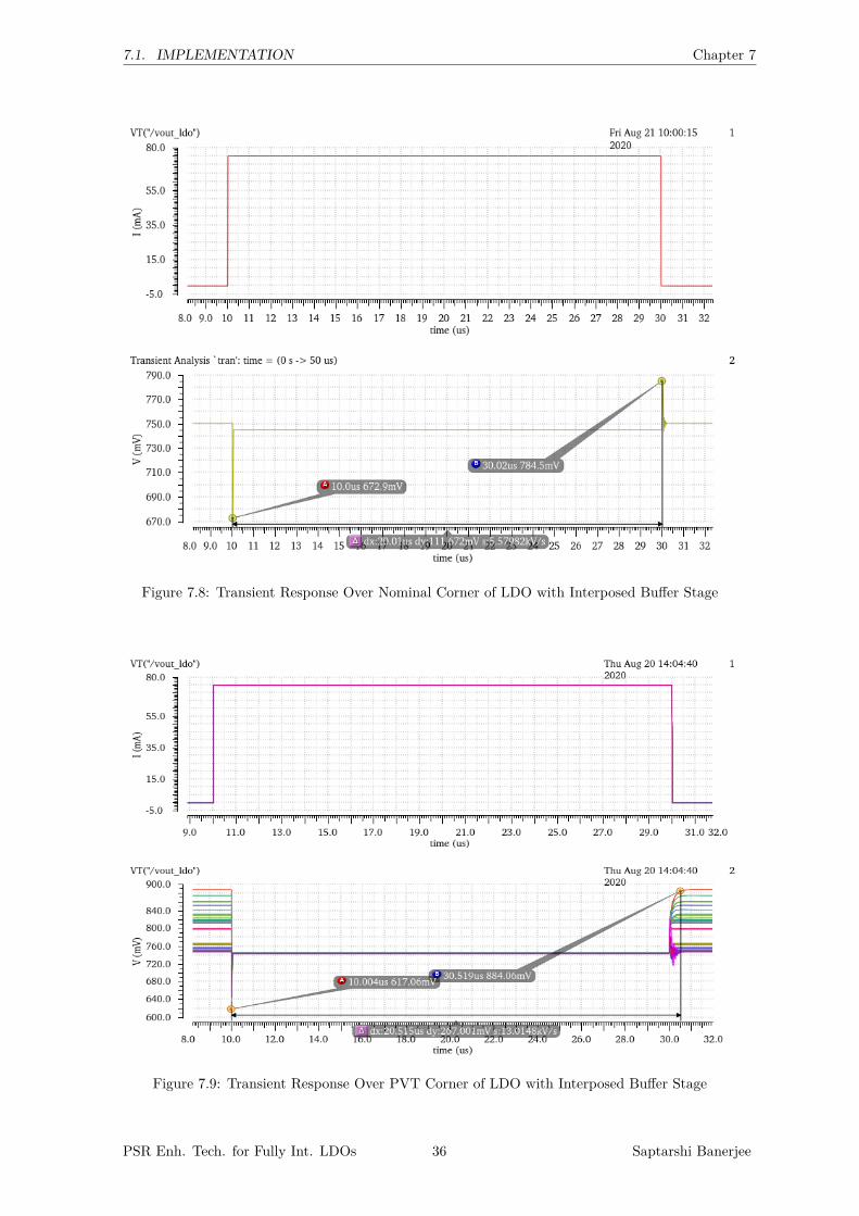
7.1.3 LDO with Interposed Buffer StageThe PSR plot of the schematic 6.2 has been illustrated in the Figure 7.7 with PSRof −9.9 dB. The transient response over nominal and PVT corner has been showedin Figure 7.8 and 7.9. The step transient was 100 µA to 75 mA in 10 ns.
Figure 7.7: PSR Plot LDO with Interposed Buffer Stage
The values from the architecture with the interposed buffer has been illustrated inthe tabulation 7.3
LDO with Interposed Buffer StageParameters Phase Margin Gain Margin UGF PSR Output Voltage DC Gain Quiescent Current
Values 59.63 9.8 243.4 M −9.9 dB 745 mV 61 dB 458 µA
Table 7.3: Results from LDO with Interposed Buffer Stage
PSR Enh. Tech. for Fully Int. LDOs 35 Saptarshi Banerjee
7.1. IMPLEMENTATION Chapter 7
Figure 7.8: Transient Response Over Nominal Corner of LDO with Interposed Buffer Stage
Figure 7.9: Transient Response Over PVT Corner of LDO with Interposed Buffer Stage
PSR Enh. Tech. for Fully Int. LDOs 36 Saptarshi Banerjee
7.1. IMPLEMENTATION Chapter 7
7.1.4 Variants of FVF-LDO7.1.4.1 FVF-LDO with Output Dominant Pole
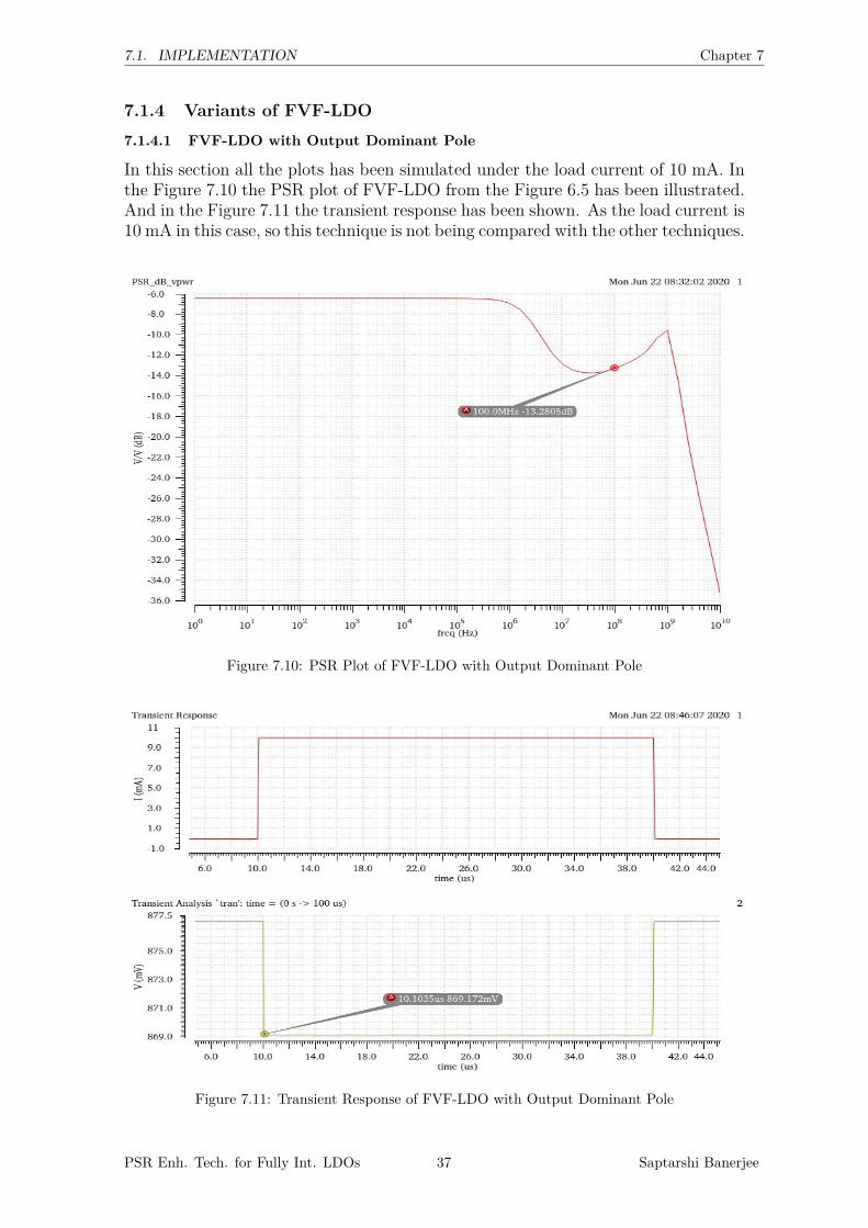
In this section all the plots has been simulated under the load current of 10 mA. Inthe Figure 7.10 the PSR plot of FVF-LDO from the Figure 6.5 has been illustrated.And in the Figure 7.11 the transient response has been shown. As the load current is10 mA in this case, so this technique is not being compared with the other techniques.
Figure 7.10: PSR Plot of FVF-LDO with Output Dominant Pole
Figure 7.11: Transient Response of FVF-LDO with Output Dominant Pole
PSR Enh. Tech. for Fully Int. LDOs 37 Saptarshi Banerjee
7.1. IMPLEMENTATION Chapter 7
7.1.4.2 FVF-LDO with Internal Dominant Pole
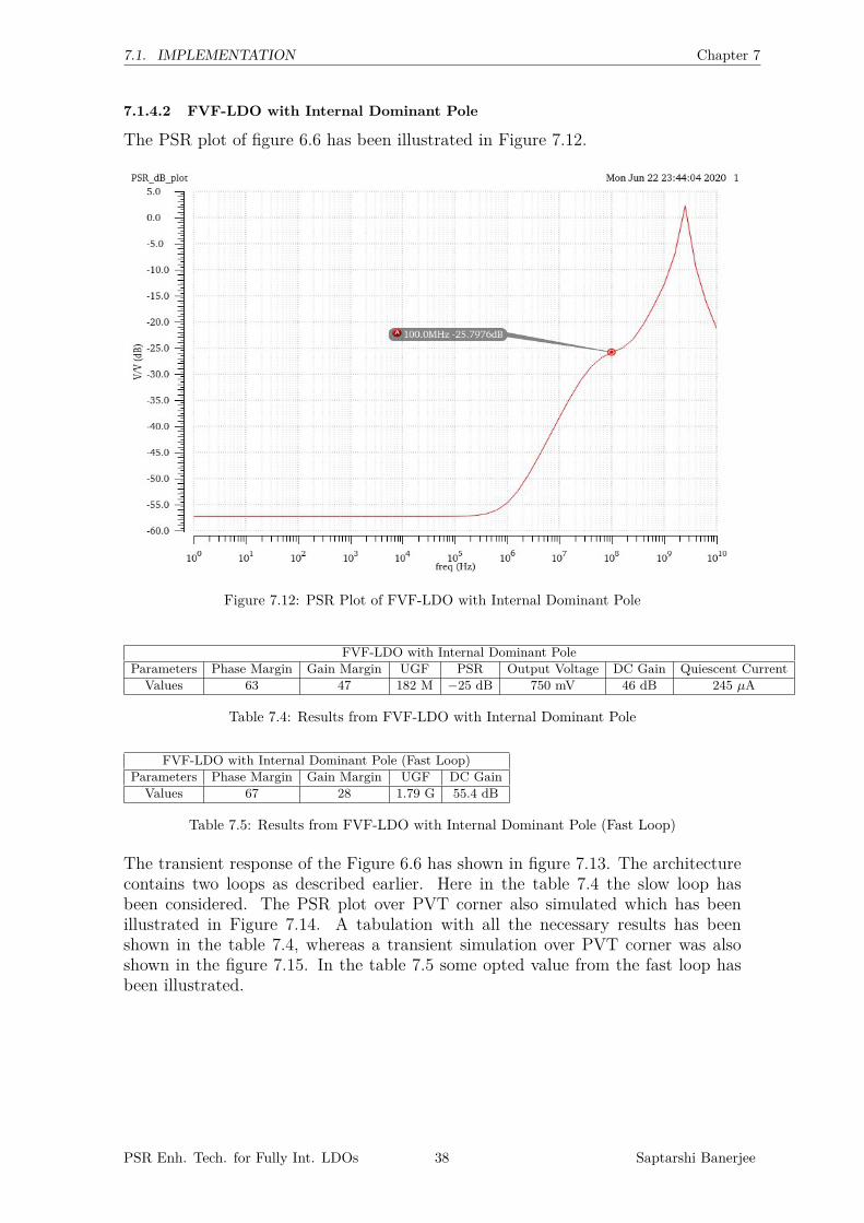
The PSR plot of figure 6.6 has been illustrated in Figure 7.12.
Figure 7.12: PSR Plot of FVF-LDO with Internal Dominant Pole
FVF-LDO with Internal Dominant PoleParameters Phase Margin Gain Margin UGF PSR Output Voltage DC Gain Quiescent Current
Values 63 47 182 M −25 dB 750 mV 46 dB 245 µA
Table 7.4: Results from FVF-LDO with Internal Dominant Pole
FVF-LDO with Internal Dominant Pole (Fast Loop)Parameters Phase Margin Gain Margin UGF DC Gain
Values 67 28 1.79 G 55.4 dB
Table 7.5: Results from FVF-LDO with Internal Dominant Pole (Fast Loop)
The transient response of the Figure 6.6 has shown in figure 7.13. The architecturecontains two loops as described earlier. Here in the table 7.4 the slow loop hasbeen considered. The PSR plot over PVT corner also simulated which has beenillustrated in Figure 7.14. A tabulation with all the necessary results has beenshown in the table 7.4, whereas a transient simulation over PVT corner was alsoshown in the figure 7.15. In the table 7.5 some opted value from the fast loop hasbeen illustrated.
PSR Enh. Tech. for Fully Int. LDOs 38 Saptarshi Banerjee

7.1. IMPLEMENTATION Chapter 7
Figure 7.13: Transient Response Over Nominal Corner of FVF-LDO with Internal Dominant Pole
Figure 7.14: PSR Plot Over PVT Corner of FVF-LDO with Internal Dominant Pole
PSR Enh. Tech. for Fully Int. LDOs 39 Saptarshi Banerjee

7.2. EVALUATION Chapter 7
Figure 7.15: Transient Response Over PVT Corner of FVF-LDO with Internal Dominant Pole
7.2 EvaluationA comparative study of all the techniques have been shown as a tabular form forreaders to get a clear view of the improvement of the PSR curve and other pa-rameters and how they are affected. It would have been interesting to see yourinterpretation of the table as well the names of the techniques has been modified intabulation to the following, Conventional LDO = Technique 1; Conventional LDOwith Improved Bandwidth = Technique 2; Conventional LDO with Inserted BufferStage = Technique 3; FVF-LDO with Internal Dominant Pole = Technique 4.
Comparison Table of All TechniquesParameter Technique 1 Technique 2 Technique 3 Technique 4Cload 200 pF 200 pF 200 pF 200 pF
Iload−max 75 mA 75 mA 75 mA 75 mAIload−slop 10 ns 10 ns 10 ns 10 ns
PSR (100 MHz) 444 mdB 2.5 dB −9.9 dB −25.79 dBVout 745 m 745 m 745 m 745 m
Quiescent Current 111 µA 442 µA 458 µA 245 µAQuiescent Power 106 µW 419 µW 435 µW 233 µW
∆Vout (mV) 427/−203 287/−144.19 77.88/−34.5 36.6/−15.99Output Noise 151 µ 208 µ 691 µ 439 µ
FoM1 1.69 ps 6.65 ps 6.90 ps 3.6 psFoM2 0.63 mV 2.5 mV 2.6 mV 1.3 mV
Table 7.6: Table of Comparison of All Techniques
PSR Enh. Tech. for Fully Int. LDOs 40 Saptarshi Banerjee

8Discussion
This chapter contains the discussion about the methods implemented and respectiveresults.
8.1 ResultsIn this section the results of the different implemented architectures have been dis-cussed. The aim of this thesis work is to design an LDO which has PSR of −25 dB at100 MHz. From the table 7.6, a comparison of all the implemented architectures hasbeen illustrated. With 75 mA output current the PSR of conventional LDO foundas 444 mdB, which is quite low as there is no added buffer stage in this architecture.But the quiescent current consumption is also low from all other techniques. Whereas the phase margin and gain margin is high, 82.11 and 31.15dB respectively. Theoutput noise is also low from other three architectures.In the improved bandwidth with the increased current ratio in current amplifier andincreased size of the transistor the PSR has improved to 2.5 dB. But some otherparameters like phase margin and gain margin has been decreased to 61.74 and 15.4dB. The improved PSR has also impacted on consuming more quiescent current andpower and increased output noise.The interposing buffer stage has helped the PSR to increase −9.9 dB, but thegain margin has been drooped below the expected value. The quiescent currentconsumption has been increased and this architecture has the large quiescent currentconsumption. The output noise is also large from other three architectures.FVF-LDO with internal dominant pole is the closest matched with the specifications.A PSR of −25 dB with moderate quiescent current consumption has been observedin this architecture. This architecture has a stable phase and gain margin of 63
and 47 dB respectively.
8.2 MethodIn this section the implemented methods have been discussed. A literature surveywith proper implementation with some modifications to meet the specifications hasbeen studied during this thesis work.In the conventional LDO architecture a PSR with slow transient response has beenobserved. A large voltage drop of 427 mV occurred in the step change of 100 µA to75 mA in 10 ns, which also resembles the slow transient response. A hump like PSRcan be observed in gate pole dominated architecture [10], as shown in Figure 7.1,PSR plot, which is located in the mid frequency band. This hump is a trade off as
41

8.2. METHOD Chapter 8
a large load current is required for this work and for chip integration a small loadcapacitor has been used. From the literature [10], we know that large load currentwill keep output pole away from gate pole. In this thesis a large load current of 75mA has been chosen whereas a output capacitor of 200 pF has been installed.To push or suppress the PSR hump some compensation techniques have been ap-plied. One of the techniques is by improving the bandwidth. To improve the band-width the current ratio in the current mirrors can be increased. The aim is to shiftthe gate pole to higher frequency but stability can be sacrificed for this as a resultswe can see the stability degradation.While pushing the gate pole to higher frequencies it can come near to the output polewhich can cause stability issues [10]. A low impedance buffer has been interposedin between error amplifier and pass device. This buffer stage has input resistance, avoltage control voltage source and a low output resistance. This current buffer willhelp to improve PSR, moreover this buffer stage will help the LDO to gain stabilityover small wide range of load current and a small load capacitor [8]. This buffer willreduce the output resistance through dynamically-biased feedback circuit. It willhelp to push the gate pole of the pass transistor at higher frequency over UGF ofthe LDO, despite having a large load current. A Miller circuit has also been usedto keep output pole away from the gate pole to maintain the stability. But a betterPSR has been achieved from this architecture under a better transient response witha voltage droop of 77.8 mV for rising edge. Although quiescent current consumptionhas been increased in this architecture.As shown in the Figure 7.10, the PSR plot is derived from an architecture of liter-ature [23], but with bit modification of the ESSF stage. Here this ESSF stage hasbeen replaced with a voltage control voltage source and an input capacitance andan output resistance to form the architecture. Where a PSR of −13 dB has beenachieved at 100 MHz. But an issue with larger load current has been observed in thisarchitecture. Here a load current of 10 mA - 20 mA has been applied to maintain thestability of the architecture. For this thesis a minimum of 75 mA current has beenneeded to meet the specifications. So, this architecture has not been considered asa comparable technique with respect to the other architectures.Furthermore, in the final technique or technique 4 in the table 7.6 a PSR of −25dB at 100 MHz has been achieved. The architecture has been motivated from theliterature [3], where two loops has been noticed, a fast loop and a slow loop. But abuffer stage has been replaced with the SSF stage [3]. A large decoupling capacitorhas been used to achieve good PSR as this capacitor will provide a clean supply tothe transistor Mp−cg. The dominant pole also formed at the gate of Mp−cg. In thisarchitecture an improved fast transient response with a voltage droop of 36mV at therising edge. The quiescent current consumption is also low from other architecturesexcept the conventional LDO architecture.
PSR Enh. Tech. for Fully Int. LDOs 42 Saptarshi Banerjee

9Conclusion and Future Work
9.1 ConclusionThis thesis work presents the design of power supply rejection enhancement tech-niques of output capacitor-less low-dropout regulators. The architectures have beendesigned in CMOS FinFET process node and cadence spectre has been used for sim-ulations .Different architectures have been optimised to meet the PSR of −25 dBat 100 MHz with the input voltage of 0.95 V to provide the output voltage of 0.75V under the load current of 75 mA, a small on chip capacitor of 200 pF has beenused as output capacitor. The architecture or FVF-LDO with internal dominantpole is the closest approximate to meet the above mentioned specifications with afast transient response.
9.2 Future WorkThis thesis work is based on implementation of different architectures to target thewide-band PSR of LDO regulators. Although on the other side some of the futurework is still can be done, which are listed below.
• Replacing ideal buffer model with a suitable low-impedance buffer circuitusing transistors.
• Further checks/simulations with the new buffer to confirm performance.• Layout design and then simulation with parasitic extracted view will be an
interesting future work to work on.
43

Bibliography
[1] K.-H. Chen, Power Management Techniques for Integrated Circuit Design. JohnWiley & Sons Incorporated, 2016.
[2] Y. Lu, Y. Wang, Q. Pan, W. Ki, and C. P. Yue, “A fully-integrated low-dropoutregulator with full-spectrum power supply rejection,” IEEE Transactions onCircuits and Systems I: Regular Papers, vol. 62, no. 3, pp. 707–716, 2015.
[3] M. Huang, H. Feng, and Y. Lu, “A fully integrated FVF-based low-dropoutregulator with wide load capacitance and current ranges,” IEEE Transactionson Power Electronics, vol. 34, no. 12, pp. 11880–11888, 2019.
[4] G. Cai, C. Zhan, and Y. Lu, “A fast-transient-response fully-integrated digitalLDO with adaptive current step size control,” IEEE Transactions on Circuitsand Systems I: Regular Papers, vol. 66, no. 9, pp. 3610–3619, 2019.
[5] C. Park, M. Onabajo, and J. Silva-Martinez, “External capacitor-less low drop-out regulator with 25 dB superior power supply rejection in the 0.4–4 MHzrange,” IEEE Journal of Solid-State Circuits, vol. 49, no. 2, pp. 486–501, 2014.
[6] P. R. Surkanti, A. Garimella, M. Manda, and P. M. Furth, “On the analysisof low output impedance characteristic of flipped voltage follower (FVF) andFVF LDOs,” in 2017 IEEE 60th International Midwest Symposium on Circuitsand Systems (MWSCAS), pp. 17–20, 2017.
[7] P. R. Surkanti, A. Garimella, and P. M. Furth, “Flipped voltage follower basedlow dropout (LDO) voltage regulators: A tutorial overview,” in 2018 31st Inter-national Conference on VLSI Design and 2018 17th International Conferenceon Embedded Systems (VLSID), pp. 232–237, 2018.
[8] M. Al-Shyoukh, H. Lee, and R. Perez, “A transient-enhanced low-quiescent cur-rent low-dropout regulator with buffer impedance attenuation,” IEEE Journalof Solid-State Circuits, vol. 42, no. 8, pp. 1732–1742, 2007.
[9] Y. Lim, J. Lee, Y. Lee, S. Song, H. Kim, O. Lee, and J. Choi, “An exter-nal capacitor-less ultralow-dropout regulator using a loop-gain stabilizing tech-nique for high power-supply rejection over a wide range of load current,” IEEETransactions on Very Large Scale Integration (VLSI) Systems, vol. 25, no. 11,pp. 3006–3018, 2017.
[10] Y. Lim, J. Lee, S. Park, Y. Jo, and J. Choi, “An external capacitorless low-dropout regulator with high PSR at all frequencies from 10 kHz to 1 GHz usingan adaptive supply-ripple cancellation technique,” IEEE Journal of Solid-StateCircuits, vol. 53, no. 9, pp. 2675–2685, 2018.
44

BIBLIOGRAPHY Chapter 9
[11] E. Sánchez-Sinencio, “Low drop-out (LDO) linear regulators: Design consider-ations and trends for high power-supply rejection (PSR),” IEEE Santa ClaraValley (SCV) Solid State Circuits Society, 2011.
[12] M. Khan and M. H. Chowdhury, “Capacitor-less low-drop out regulator (ldo)with improved psrr and enhanced slew-rate,” in 2018 IEEE International Sym-posium on Circuits and Systems (ISCAS), pp. 1–5, 2018.
[13] Wenguan Li, Ruohe Yao, and Lifang Guo, “A CMOS low drop out regulatorwith high power supply rejection,” in 2009 IEEE International Conference ofElectron Devices and Solid-State Circuits (EDSSC), pp. 384–387, 2009.
[14] A. Veeravalli and S. M. Nolan, “Introduction to low dropout (LDO) linearvoltage regulators,” tech. rep., Vidatronic,Inc, 2017.
[15] B. S. Lee, “Understanding the terms and definitions of LDO voltage regulators,”tech. rep., Texas Instrument, 1999.
[16] G. A. Rincon-Mora, “Current efficient, low voltage, low drop-out regulators,”Master’s thesis, Georgia Institute of Technology, 1996.
[17] M. Tiikkainen, “LDO voltage regulator for on-chip power management,” Mas-ter’s thesis, University of Oulu, 2014.
[18] P. Hazucha, T. Karnik, B. A. Bloechel, C. Parsons, D. Finan, and S. Borkar,“Area-efficient linear regulator with ultra-fast load regulation,” IEEE Journalof Solid-State Circuits, vol. 40, no. 4, pp. 933–940, 2005.
[19] J. Guo and K. N. Leung, “A 6-µ w chip-area-efficient output-capacitorless LDOin 90-nm CMOS technology,” IEEE Journal of Solid-State Circuits, vol. 45,no. 9, pp. 1896–1905, 2010.
[20] K. Mori, Y. Okuma, X. Zhang, H. Fuketa, T. Sakurai, and M. Talamiya,“Analog-assisted digital low dropout regulator (AAD-LDO) with 59 % fastertransient response and 28 % ripple reduction,” International Conference onSolid State Devices: Extended Abstracts of the 2013, 2013.
[21] J. C. Teel, “Understanding power supply ripple rejection in linear regulators,”Texas Instruments Analog applications journal, 2005.
[22] P. S. Pedro Fernandes, Julio Paisana, “High PSRR low drop-out voltage regula-tor (LDO),” Master’s thesis, Instituto Superior Tecnico Electrical EngineeringDepartment Technical University of Lisbon, Lisbon, Portugal, 2009.
[23] Y. Lu, C. Li, Y. Zhu, M. Huang, S. U, and R. P. Martins, “A 312 ps response-time LDO with enhanced super source follower in 28 nm CMOS,” ElectronicsLetters, vol. 52, no. 16, pp. 1368–1370, 2016.
[24] B. Yang, B. Drost, S. Rao, and P. K. Hanumolu, “A high-PSR LDO using afeedforward supply-noise cancellation technique,” in 2011 IEEE Custom Inte-grated Circuits Conference (CICC), pp. 1–4, 2011.
PSR Enh. Tech. for Fully Int. LDOs 45 Saptarshi Banerjee
![Инструкция Yamaha PSR-E453PSR-E453/PSR-EW400 7 + " , . 4 " [ ] ( 5 .) ( 6&- " ), " . $ , . # "](https://img.pdfslide.us/doc/110x75/60dceb7003bf806879693103/f-yamaha-psr-e453-psr-e453psr-ew400-7-4-.jpg)