Embed Size (px)
Citation preview

PLDshell Plus
™/PLDasm
™ U
ser’s Guide V5.0 PLDshell Plus™/PLDasm™
User’s Guide V5.0®
®
PLDshell cover 7/10/96 5:20 PM Page 1 (2,1)
om
pile
r C
om
man
ds
for
FL
EX
log
icF
un
ctio
ns
PLDshell Plus/PLDasm User’s Guide 6-1
Chapter 6 — Compiler Commands for FLEXlogic Functions
This chapter describes specific PLDshell compiler commands that can be used to takeadvantage of the various properties of the FLEXlogic device family. Some examples ofhow these functions may be implemented are provided in each section that follows. Formore information on device architectures, refer to the individual device data sheets.
SRAM
The SRAM module is specified in the pin list by using the RAM keyword:
PIN BUFRAM[9:0] RAM ; The SRAM module outputs
The SRAM module can also be declared as a node if its outputs will only be used internally:
NODE BUFRAM[9:0] RAM ; The SRAM module as buried nodes
Then in the design specification the SRAM controls will use the label BUFRAM:
BUFRAM[9:0].DATA = DIN[9:0] ; The SRAM data inputs, all 10BUFRAM[6:0].ADDR = A[6:0] ; The SRAM address lines, all 7BUFRAM.BE = ENABLE_ ; The SRAM block-enableBUFRAM.WE = WR_ ; The SRAM write-enableBUFRAM.TRST = OE_ ; The SRAM output-enable
NOTE:
These three control signals are active low: .BE, .WE, and .TRST.Therefore, all equations for RAM must be stated in active-low form forall FLEXlogic devices except the EPX8160, which can have active-lowor active-high control signals.
If the design does not require all of the address or data lines, then you can just specify thosewhich are used. For example, if a 16-word SRAM is needed, then specify just four addresslines:
BUFRAM[3:0].ADDR = A[3:0] ; The SRAM address lines, use 4
Similarly, if not all of the data lines are needed, then just specify those that are used:
PIN BUFRAM[6:0] RAM ; The SRAM module outputs, use 7
EQUATIONSBUFRAM[3:0].DATA = DIN[3:0] ; SRAM data inputs that are usedBUFRAM[9:4].DATA = GND ; unused SRAM data inputsBUFRAM[3:0].ADDR = A[3:0] ; SRAM address inputsBUFRAM[6:4].ADDR = GND ; unused SRAM address inputs
C

Co
mp
iler
Co
mm
and
sfo
r F
LE
Xlo
gic
Fu
nct
ion
s
NOTE:
6-2 PLDshell Plus/PLDasm User’s Guide
Fti
It’s good design practice to connect unused input signals to GND. Forthose SRAM data or address inputs which are not used in the design,specify a GND signal for the connection:
Even though some of the SRAM capability is not used in a design, the unused cells are notavailable for logic functions. This is because the entire CFB changes to provide the SRAMcapability.
This is summarized below:
/DOUT.WE = VCC;Read from SRAM orDOUT.WE = GND;Read from SRAM/DOUT.TRST = GND;Output enabled/DOUT.BE = GND;Block enabled
SRAM Initialization
The initial data stored in the SRAM at power-up can be specified in the design with the useof the RAM_DEFAULTS keyword as follows:
RAM_DEFAULTS BUFRAM 0 : 0x155 [0xF:0x1] : 0x233 [0x7F:0x10] : 0x0
The address of the location to be initialized is placed on the left side of the colon, and thedata for that address is placed on the right side. In the above example, location 0 has thedata value 155H (Hexadecimal), locations 1 to F have the value 233H, and locations 10Hto 7FH have the value 0. If the entire RAM is to be initialized with just one value, thekeyword DEFAULT_VALUE can be used:
RAM_DEFAULTS BUFRAM DEFAULT_VALUE 0x155
This will initialize all locations of the SRAM to the value 155H.
Comparator
The comparator is specified by the use of the .CMP extension. For example, the followingequation compares two 4-bit words:
PIN COMP_OUT ;comparator outputCOMP_OUT.CMP = [ A[3:0] ] == [ B[3:0] ]
The macrocell incorporating the comparator output is labelled COMP_OUT. Thecomparison equation then uses the .CMP extension to call for the comparator function.
To add other product terms to this macrocell, just use the pin name and add the appropriatefunction:

om
pile
r C
om
man
ds
for
FL
EX
log
icF
un
ctio
ns
PLDshell Plus/PLDasm User’s Guide 6-3
PIN IOR ; I/O READ strobe, active-HIGHPIN IOW ; I/O WRITE strobe, active-HIGHCOMP_OUT = IOW * IOR ; I/O strobes of a busCOMP_OUT.CMP = [ A[3:0] ] == [ B[3:0] ]
In the above example, COMP_OUT will be active (high) when IOR and IOW are active orthe comparator output is active. Note that the output of the comparator can be inverted sothat it can logically AND with other signals in the macrocell OR gate. In this way, a decodercan be designed for an I/O access from a microcomputer bus, or other operations requiringa comparison ANDed with other logical functions.
If the output function needs to be registered, use the .D extension on the signal name:
COMP_OUT.D := IOW * IOR ; Registered output selectedCOMP_OUT.CMP = [ A[3:0] ] == [ B[3:0] ]
Where the possible values would be:
And internally the nodes would be configured at the pin:
a. On the rising edge of the clock.
IOW IOR COMP_OUT.D COMP_OUT.CMP Qa
0 0 0 0 0
0 0 0 1 1
0 1 0 0 0
0 1 0 1 1
1 0 0 0 0
1 0 0 1 1
1 1 1 0 1
1 1 1 1 1
Clock
COMP_OUT.D
COMP_OUT.CMPD Q
C

Co
mp
iler
Co
mm
and
sfo
r F
LE
Xlo
gic
Fu
nct
ion
s
6-4 PLDshell Plus/PLDasm User’s Guide
Fti
Clock Options
Altera’s FLEXlogic family1 offers three modes for clocking registers: synchronous,synchronous delayed, and asynchronous. Either polarity of a clock can be used as an inputto the macrocell, meaning that macrocells can clock on opposite edges of a master clock.There are two synchronous clocks, which are global, meaning they are available to all CFBsin the device, and are sourced by the two clock pins on the package. The synchronousdelayed clock means that the clock is delayed slightly before being applied to themacrocell. This changes the setup and hold time requirements of signals applied to the inputof the macrocell. If the data input to a flip-flop does not meet the setup or hold-timerequirement of the flip-flop, the output of the flip-flop is indeterminate after the clock edge.In the worst case, the output of the flip-flop may enter a metastable state, where it is neitherhigh nor low. This causes unpredictable results to any logic connected to the flip-flop. Thusin a marginal situation, the ability to delay the clock can make the operation more reliable.
The delayed synchronous clock is applied to all the macrocells in a CFB using that clocksignal.
The third clocking option is asynchronous. This means that any signal that enters the CFBcan be used to clock the macrocell via a single p-term. The limit is that in any CFB therecan be only two different asynchronous clocks.
The design file requirements are illustrated below. First, specify the synchronous clockpins, using the actual pin number of the device:
PIN 3 CLK1 ; One of the synchronous clocksPIN 45 CLK2 ; The other synchronous clock pin
Specify the output names:
PIN FLOP1 ; One flip-flopPIN FLOP2 ; The other flip-flop
Now, when setting the synchronous clock of the flip-flops, use the appropriate name:
FLOP1.CLKF := /CLK1 ; Select the first clock as invertedFLOP2.CLKF := CLK2 ; Use the other clock for this flip-flop
If the delayed synchronous clock is desired, use the DELAYCLK keyword in the PINspecification:
PIN FLOP1 DELAYCLK ; Use the delayed clock option
Any other macrocell in the same CFB as FLOP1 that specifies the same clock pin (CLK1)must also have a delayed clock.
If an asynchronous clock is desired, use the signal name desired for the clock:
FLOP3.ACLK = FLOP1 ; Use the output of the first flip-flop
1. Devices EPX8160, EPX780, and EPX740 inclusive.
om
pile
r C
om
man
ds
for
FL
EX
log
icF
un
ctio
ns
NOTE:
PLDshell Plus/PLDasm User’s Guide 6-5
( A delayed clock option is not available in the asynchronous mode.)
Multiple Clock Pin Support
The EPX8160 has two clocks for each half of the device. It may be desired to use the sameclock signal in two different halves of the device. This may occur due to a large number ofmacrocells using the same clock signal. The MPIN keyword can be used to specify oneclock signal feeding multiple device groups. It is used in place of the PIN keyword in theDeclaration section of a PLDasm file.
Syntax
The syntax of the MPIN command is very similar to the PIN command. The only differenceis two pin numbers are specified in vector format instead of one. The pins can be thephysical clock pin numbers from the device, or the symbolic datasheet names.
Two examples of the syntax are shown below. The first example specifies the actual pinnumbers on the EPX8160 for CLK1 and CLK4. The second example uses the symbolicdatasheet clock pin names to specify the desired clock signals.
MPIN [184, 80] CLOCK_SIG ; Using pin numberMPIN [CLK1, CLK4] CLOCK_SIG ; Using datasheet names
Group Feature
One architectural feature of the EPX8160 is to offer you the choice of which half of thedevice you want to put logic into. The benefit of this feature is that it is now possible toreconfigure one part of the device while the rest of the device is still running. Thiscapability is called group reconfiguration.
To take advantage of the new group reconfiguration capability, a new PLDasm languagecommand was created called the GROUP command. The EPX8160 has two ConfigurationGroups (CGs): 8160_0 and 8160_1, and the GROUP command allows you to target outputsto one CG or the other.
Syntax
The syntax of the GROUP command is (following the PIN or NODE number and name):
GROUP CGx
where CG is the Configuration Group and x is either 0 or 1, specifying one half of the deviceor the other. In the example below, logic is directed to two different CGs of the device.AOUT can be assigned to any macrocell pins in CG0 and BOUT can be assigned to anymacrocell in CG1.
C

Co
mp
iler
Co
mm
and
sfo
r F
LE
Xlo
gic
Fu
nct
ion
s
PIN AOUT REG GROUP CG0
6-6 PLDshell Plus/PLDasm User’s Guide
Fti
NODE BOUT COMB GROUP CG1
Default Group
If the GROUP command is not used with the PIN or NODE commands, the fitter will placethe macrocell in whichever group provides the best fit for the design.
Limitations and Error Conditions
• The GROUP command is understood by the fitter only when targeting designs to theEPX8160. If the command is used when targeting any other Altera device, the attributewill be ignored.
• Pin assignments made to a pin not in the configuration group will produce an error andthe fit will not be completed until corrected.
• Assignments made to an invalid Configuration Group value (e.g., CG3) will producean error and the fit will not be completed until corrected.
Output Options
The FLEXlogic family offers three output options: 3VOLT, 5VOLT, and OPEN_DRAIN.While the 3VOLT and 5VOLT output options are actually controlled by the voltage appliedto the CFB supply pin on the device, these keywords tell the compiler to group similaroutput signals in the same CFB. This allows the use of both 3VOLT and 5VOLT outputsfrom the same device. The OPEN_ DRAIN option tells the compiler to enable the open-drain output drive of the macrocell. This is on a macrocell basis, and does not affect theother macrocells in the same CFB. Use the appropriate keyword in the PIN declaration. Thedefault is 5 volts.
PIN OUT1 5VOLT ; 5-volt TTL or CMOS drive groupPIN OUT2 3VOLT ; 3-volt TTL or CMOS drive groupPIN OUT3 OPEN_DRAIN ; Open-drain output, wire-OR is possible
Clear/Preset Control Functions
To use the clear or preset option, just use the .RSTF or .SETF extension with the macrocellname:
FLOP3.RSTF = RESET ; Output will be LOW when RESET activeFLOP4.SETF = RESET ; Output will be HIGH when RESET active
These functions can also be built as one product term:
FLOP3.RSTF = RESET * /GO * STATE3
om
pile
r C
om
man
ds
for
FL
EX
log
icF
un
ctio
ns
Alternatively, a STRING function can define the clear or preset logic term, to make the
PLDshell Plus/PLDasm User’s Guide 6-7
design file more concise,
STRING RESET_FLOP ' ( RESET * /GO * STATE3 ) '
then
FLOP3.RSTF = RESET_FLOP
Product-Term Allocation
In most programmable-logic designs, the average macrocell uses only a few product terms.The FLEXlogic device macrocells take advantage of this by providing product-termallocation among the macrocells of the CFB. Each macrocell can take unused product termsfrom adjacent macrocells. The two outside macrocells of a CFB can have up to 16 p-terms,including two that can be borrowed from the adjacent macrocell (see Figure 6-1). The innermacrocells have the ability to use up to 8 product terms by using 2 from each neighboringmacrocell (see Figure 6-1).
C

Co
mp
iler
Co
mm
and
sfo
r F
LE
Xlo
gic
Fu
nct
ion
s
6-8 PLDshell Plus/PLDasm User’s Guide
Fti
Figure 6-1 CFB Product Term Re-Allocation
The limitations of product-term allocation are that there may be combinations of pins andmacrocells that can’t compile because the logic dictates the use of more product terms thancan be provided to a specific macrocell. The easiest method to avoid this circumstance isto design the logic of the project without specifying pin numbers. This allows the compilerto place macrocells for the best use of the product terms available.
For designs which have committed pin numbers, or when upgrading an existing design, ifthe compiler reports that there are not enough product terms available, you need to makelogic changes. Very often, changing the states of a state machine design will re-allocateproduct terms favorably. Alternatively, you can add states and associated flip-flops to thedesign to reduce the size of the product terms needed to gate the various states. Use ofmacrocells 0 and 9 will provide 16 product terms each which may be achieved through re-assignment of functions in the design.
12
2 MCELL #0
A=B2
2 MCELL #1
A=B
A=B
2 MCELL #9
A=B2
2 MCELL #8
A=B
A=B
12

om
pile
r C
om
man
ds
for
FL
EX
log
icF
un
ctio
ns
Adding intermediate macrocells to complex functions increases the number of product
PLDshell Plus/PLDasm User’s Guide 6-9
terms available to implement the function (see Figure 6-2).
Figure 6-2 Adding Intermediate Macrocells
BEFORE
8 P-TERMS
8 P-TERMS
AFTER
M-CELL1 P-TERM
C

Co
mp
iler
Co
mm
and
sfo
r F
LE
Xlo
gic
Fu
nct
ion
s
6-10 PLDshell Plus/PLDasm User’s Guide
Fti

Mo
du
les
and
Hie
rarc
hic
al D
esig
n
PLDshell Plus/PLDasm User’s Guide 7-1
Chapter 7 — Modules and Hierarchical Design
Hierarchical design is the process of breaking a large design into smaller and smaller pieces(called modules). The smaller modules are easier to understand, test, and can be referencedas needed from the higher level design or grouped into libraries for use in other designs.
When functional blocks are used repetitively in a design, such as a counter, making thecounter into a module saves writing its equations each time it is used. Thus the design filebecomes more concise, and easier to read and understand.
Defining a Module
Modules can be defined in two basic forms. Existing .PDS designs can be used as moduledefinitions without any changes.
Alternatively if a module is defined in the same file as the design that is using it, or if thereis more than one module definition in a file, the module definition is enclosed withDEFMOD and ENDMOD keywords. The body of the module definition is .PDSstatements. Only one state machine can be used for each defined by a DEFMOD statement.
There are three different module definition forms defined and pictured below.
1. The first module definition form uses the existing file. It looks like this:
<PDS statements — independent design>
Figure 7-1 is an example of this first module definition form.
Figure 7-1 High Level .PDS Design (Referenced as a Module)
Title: This file (clkedinv.pds) is an example of a self contained (high level) design that is used as a module definition. It also contains a buried node “buried” that is not referenced by the high level design (see modtop.pds). The design performs a clocked inversion of its input.
CHIP clk_invert EP22v10
PIN clkPIN inPIN outNODE buried; just added for INST example in modtop.pds
EQUATIONS
/buried := inburied.CLKF = clkout = buried.FB

Mo
du
les
and
Hie
rarc
hic
al D
esig
n
2. The second form contains module definitions only (e.g., a library). It would look like
7-2 PLDshell Plus/PLDasm User’s Guide
this:
HeaderDEFMOD mymodule ( ...module arguments...)PDS statements -- defining module>ENDMOD ... (other module definitions)
Figure 7-2 lists GATE.PDS, which shows this module definition form.
Figure 7-2 Multiple Module Definitions in a File
3. The third form uses module definitions in the same file as the one referencing thedesign. An example of this follows:
Header...
DEFMOD mymodule ( ...module arguments...)<PDS statements -- defining module>ENDMOD
... (other module definitions)...CHIP ... (for referencing -- high level -- design)...High level design
Title: This file (gate.pds) contains two module definitions: myxor, mycmp. It is an example of multiple level (nested) module references -- the module definition for “mycmp” references the module “myxor”.
; define a module “myxor” to XOR two inputs and produce one output;DEFMOD myxor ( in[1:2], out )CHIP modxor ALTERA_ARCHPIN in[1:2]PIN outEQUATIONSout = in1 * /in2 + /in1 * in2ENDMOD
;; define a module “mycmp” to perform a 2-bit compare using “myxor”;DEFMOD mycmp (a[1:2],b[1:2],cmp[1:2])CHIP modcmp ALTERA_ARCHPIN a[1:2]PIN b[1:2]PIN cmp[1:2]MODULE myxor (in1=a1, in2=b1, out=cmp1)MODULE myxor (in1=a2, in2=b2, out=cmp2)ENDMOD

Mo
du
les
and
Hie
rarc
hic
al D
esig
n
Figure 7-3 shows a sample of this third form of module definition.
PLDshell Plus/PLDasm User’s Guide 7-3
Figure 7-3 High Level Design with Module Reference
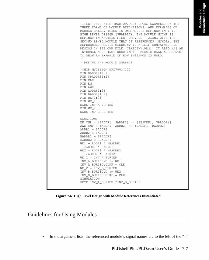
Title: This file (modtop.pds) shows examples of the three forms of module definitions, and examples of module calls. There is one module defined in this high level design (swapbit). The module mycmp is defined in another file (cmp.pds), along with the second level module that it references (myxor). The referenced module clkedinv is a self contained PDS design in its own file (clkedinv.pds). It also has an internal node (not used in the module call arguments) to show an example of how instance is used.
;; define the module swapbit;DEFMOD swapbit ( in[1:2], out[1:2] )CHIP filemod ALTERA_ARCHPIN in[1:2]PIN out[1:2]EQUATIONS
out[1:2] = in[2:1]ENDMOD
CHIP MYDESIGN EPX780QC132
PIN saddr[1:2]PIN sbaddr[1:2]PIN addr[1:2]PIN baddr[1:2]PIN we[1:2]PIN clkPIN enPIN awk;; high level design equation;EQUATIONS
en.CMP = [ saddr[1:2] ] == [ sbaddr[1:2] ]
;; create two instances of the swapbit module ; (defined in this file);MODULE swapbit ( in[1:2] = saddr[1:2], out[1:2] = addr[1:2] )MODULE swapbit ( in[1:2] = sbaddr[1:2], out[1:2] = baddr[1:2] )
;; create one instance of the mycmp module (defined in file cmp.pds);
MODULE mycmp FILE cmp (a[1:2]=addr[1:2], b[1:2]=baddr[1:2],

Mo
du
les
and
Hie
rarc
hic
al D
esig
n
7-4 PLDshell Plus/PLDasm User’s Guide
Figure 7-3 High Level Design with Module References (Continued)
Referencing a Module Definition
Regardless of which form is used to define a module, it can be referenced by any otherdesign. A module instance (reference) is created by using the MODULE statement. Themodule statement has the general form:
MODULE <module name> [ INSTANCE <instance name> ] [FILE <file name>] (<argument list> )
The module name is the name used in the module definition on the DEFMOD statement.For an existing .PDS design referenced as a module, the module name is the .PDS filename—without extension.
For example:
MODULE clkedinv INST inv_a ( in = we1, out = we_1, clk = clk )
;; create one instance of the mycmp module (defined in file cmp.pds);MODULE mycmp FILE cmp (a[1:2]=addr[1:2], b[1:2]=baddr[1:2], cmp[1:2]=we[1:2])
;; create two instances of the clkedinv module -- a self-contained PDS file; (two instance name -- inv_a and inv_b -- are used to document which ; instance of the internal signal “buried” goes with which MODULE reference;MODULE clkedinv INST inv_a ( in = we1, out = we_1, clk = clk )MODULE clkedinv INST inv_b ( in = we2, out = we_2, clk = clk )
;; need a new “EQUATION” section for equations following module references;EQUATIONS
awk.CMP = [ addr[1:2] ] == [ baddr[1:2] ]
;; The instance names (e.g. inv_a) can be used to simulate nodes; that are internal to modules;SIMULATION
SETF inv_a_buried /inv_b_buried

Mo
du
les
and
Hie
rarc
hic
al D
esig
n
The instance name is the name used to identify a particular module instance. It is useful in
PLDshell Plus/PLDasm User’s Guide 7-5
designs where there are multiple instances of the same module. By defining an instancename, nodes within a referenced module can be simulated—even though they are internalto the module. Also in report files, it is possible to track which module references createdthe internal nodes.
For example:
MODULE clkedinv INST inv_b ( in = we2, out = we_2, clk = clk )...SIMULATIONSETF inv_a_buried /inv_b_buried
The file name is used whenever the module being referenced is not in the referencing file,and the module name is not the same as the file name. This is typically the case whenmultiple modules have been defined in the same file—as in a library.
For example:
MODULE mycmp FILE cmp (a[1:2]=addr[1:2], b[1:2]=baddr[1:2],cmp[1:2]=we[1:2])
If the module being referenced is in another file it is considered an external reference. (SeeFigure 7-4, Referencing a Module—Internal Reference.) If it is in the same file, it is aninternal reference. (See Figure 7-5, Referencing a Module—External Reference.) Bothinternal and external references can be made from within the same file.
Figure 7-4 Referencing a Module—Internal Reference
MODTOP.PDS
SWAPBIT

Mo
du
les
and
Hie
rarc
hic
al D
esig
n
7-6 PLDshell Plus/PLDasm User’s Guide
Figure 7-5 Referencing a Module—External Reference
The argument list is used to map the signals from the high-level design into the modulebeing referenced. The referenced module signal name must be to the left of the “=” and thereferencing signal name on the right.
For example:
MODULE swapbit ( in[1:2]=saddr[1:2], ...
in[1:2] are two signals in the referenced module swapbit. They are associated with thereferencing design signal names saddr[1:2].
Module Example
The following example demonstrates the different module definition methods, and showshow a module is referenced. The high-level (referencing) design is in a file calledMODTOP.PDS. It references three different modules. The first, “swapbit,” is defined in thesame file (MODTOP.PDS). The second module is defined in a separate file (CMP.PDS)using the DEFMOD/ENDMOD construct. The third module is a self-contained .PDSdesign in a third file (CLKEDINV.PDS). The module defined in CMP.PDS is an exampleof nested module references. The resulting .PDS design with the module referencesinstantiated is shown in Figure 7-6.
MODTOP.PDS
MYCMP
(CMP.PDS)
CLKEDINV
(CLKENDINV.PDS)
Mo
du
les
and
Hie
rarc
hic
al D
esig
n
PLDshell Plus/PLDasm User’s Guide 7-7
Figure 7-6 High Level Design with Module References Instantiated
Guidelines for Using Modules
• In the argument lists, the referenced module’s signal names are to the left of the “=”
TITLE: THIS FILE (MODTOP.PDS) SHOWS EXAMPLES OF THE THREE FORMS OF MODULE DEFINITIONS, AND EXAMPLES OF MODULE CALLS. THERE IS ONE MODULE DEFINED IN THIS HIGH LEVEL DESIGN (SWAPBIT). THE MODULE MYCMP IS DEFINED IN ANOTHER FILE (CMP.PDS), ALONG WITH THE SECOND LEVEL MODULE THAT IT REFERENCES (MYXOR). THE REFERENCED MODULE CLKEDINV IS A SELF CONTAINED PDS DESIGN IN ITS OWN FILE (CLKEDINV.PDS). IT ALSO HAS AN INTERNAL NODE (NOT USED IN THE MODULE CALL ARGUMENTS) TO SHOW AN EXAMPLE OF HOW INSTANCE IS USED.;; DEFINE THE MODULE SWAPBIT::CHIP MYDESIGN EPX780QC132PIN SADDR[1:2] PIN SBADDR[1:2] PIN CLK PIN EN PIN AWK PIN ADDR[1:2] PIN BADDR[1:2] PIN WE[1:2] PIN WE_1 NODE INV_A_BURIEDPIN WE_2NODE INV_B_BURIED
EQUATIONSEN.CMP = [SADDR1, SADDR2] == [SBADDR1, SBADDR2]AWK.CMP = [ADDR1, ADDR2] == [BADDR1, BADDR2]ADDR1 = SADDR2ADDR2 = SADDR1BADDR1 = SBADDR2BADDR2 = SBADDR1WE1 = ADDR1 * /BADDR1+ /ADDR1 * BADDR1WE2 = ADDR2 * /BADDR2 + /ADDR2 * BADDR2WE_1 = INV_A_BURIEDINV_A_BURIED.D := WE1INV_A_BURIED.CLKF = CLKWE_2 = INV_B_BURIEDINV_B_BURIED.D := WE2INV_B_BURIED.CLKF = CLKSIMULATIONSETF INV_A_BURIED /INV_B_BURIED
Mo
du
les
and
Hie
rarc
hic
al D
esig
n
and the high-level design signal names are to the right. Signals cannot be inverted (“/”)
7-8 PLDshell Plus/PLDasm User’s Guide
in the module argument lists.
• The pin declarations must have consistent polarity between the high-level design andthe referenced modules.
• Signals that are not used (passed) through the module argument list are treated asinternal to the module being referenced. They will not be connected to the higher leveldesign.
• Only the Simulation section from the high level design is processed.
• STRING definitions within a module definition apply only to that module. STRINGstatements in the high-level design apply to the high-level design and all of thereferenced modules.

Usi
ng
th
e U
tilit
yP
rog
ram
s
PLDshell Plus/PLDasm User’s Guide 8-1
Chapter 8 — Using the Utility Programs
PLDshell Plus provides utility programs for processing files between different source andtarget file formats. This section describes how to use the Disassembly, Conversion,Translation, and Merge utilities.
Disassembly
The disassembly program processes a JEDEC file and creates a .PDS source file. While theJEDEC file can be used for a supported non-Altera device; the resulting disassembled .PDSsource file can be used only for an Altera device. Disassembly of some, but not all, AlteraPLD JEDEC files is also supported.
• The options available on the Disassemble sub-menu are as follows:
Input Filename — This is the JEDEC input file with the .JED extension.
Source Device — This is the source device for which the JEDEC file was originallygenerated. Pressing the <Space> key displays a list of supported source devices.Once the source device is selected, the target Altera device is automatically selectedand displayed on the right.
Package Type — Sets the package type. Pressing the <Space> key displays a list ofpackage types for the device selected in the Source Device field.
Output Filename — Displays the output file name that will be created duringdisassembly. The default is the target device name plus the .PDS extension.
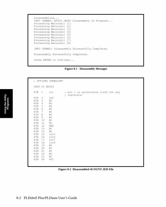
Figure 8-1, Disassembly Messages, shows the messages displayed during disassembly.Figure 8-2, Disassembled 4COUNT.JED File, shows a .PDS file created from the4COUNT.JED file (created by compiling the 4COUNT.PDS file in your installationdirectory). This is a simple design using two inputs and four I/O macrocells to implementa 4-bit counter.
Usi
ng
th
e U
tilit
y P
rog
ram
s
8-2 PLDshell Plus/PLDasm User’s Guide
Figure 8-1 Disassembly Messages
Figure 8-2 Disassembled 4COUNT.JED File
Disassembling...INFO JDBMAC: EP224 JEDEC Disassembly in Progress...Processing Macrocell [1]Processing Macrocell [2]Processing Macrocell [3]Processing Macrocell [4]Processing Macrocell [5]Processing Macrocell [6]Processing Macrocell [7]Processing Macrocell [8]
INFO JDBMAC: Disassembly Successfully Completed.
Disassembly Successfully Completed.
Press ENTER to Continue...
; OPTIONS TURBO=OFF
CHIP U1 EP224
PIN 1 in1 ; pin 1 is synchronous clock for any; registers.
PIN 2 in2PIN 3 NCPIN 4 NCPIN 5 NCPIN 6 NCPIN 7 NCPIN 8 NCPIN 9 NCPIN 10 NCPIN 11 NCPIN 12 GNDPIN 13 NCPIN 14 NCPIN 15 io15PIN 16 io16PIN 17 io17PIN 18 io18PIN 19 NCPIN 20 NCPIN 21 NCPIN 22 NCPIN 23 NCPIN 24 VCC
Usi
ng
th
e U
tilit
yP
rog
ram
s
PLDshell Plus/PLDasm User’s Guide 8-3
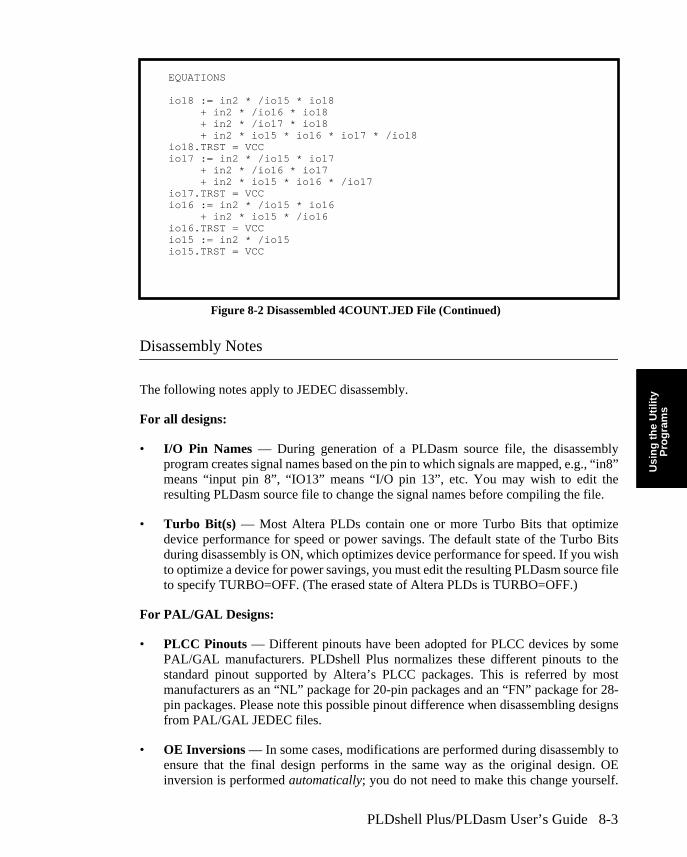
Figure 8-2 Disassembled 4COUNT.JED File (Continued)
Disassembly Notes
The following notes apply to JEDEC disassembly.
For all designs:
• I/O Pin Names — During generation of a PLDasm source file, the disassemblyprogram creates signal names based on the pin to which signals are mapped, e.g., “in8”means “input pin 8”, “IO13” means “I/O pin 13”, etc. You may wish to edit theresulting PLDasm source file to change the signal names before compiling the file.
• Turbo Bit(s) — Most Altera PLDs contain one or more Turbo Bits that optimizedevice performance for speed or power savings. The default state of the Turbo Bitsduring disassembly is ON, which optimizes device performance for speed. If you wishto optimize a device for power savings, you must edit the resulting PLDasm source fileto specify TURBO=OFF. (The erased state of Altera PLDs is TURBO=OFF.)
For PAL/GAL Designs:
• PLCC Pinouts — Different pinouts have been adopted for PLCC devices by somePAL/GAL manufacturers. PLDshell Plus normalizes these different pinouts to thestandard pinout supported by Altera’s PLCC packages. This is referred by mostmanufacturers as an “NL” package for 20-pin packages and an “FN” package for 28-pin packages. Please note this possible pinout difference when disassembling designsfrom PAL/GAL JEDEC files.
• OE Inversions — In some cases, modifications are performed during disassembly toensure that the final design performs in the same way as the original design. OEinversion is performed automatically; you do not need to make this change yourself.
EQUATIONS
io18 := in2 * /io15 * io18 + in2 * /io16 * io18 + in2 * /io17 * io18 + in2 * io15 * io16 * io17 * /io18io18.TRST = VCCio17 := in2 * /io15 * io17 + in2 * /io16 * io17 + in2 * io15 * io16 * /io17io17.TRST = VCCio16 := in2 * /io15 * io16 + in2 * io15 * /io16io16.TRST = VCCio15 := in2 * /io15io15.TRST = VCC
Usi
ng
th
e U
tilit
y P
rog
ram
s
When modifications like this occur, a message is displayed on the screen and a
8-4 PLDshell Plus/PLDasm User’s Guide
comment is placed in the PLDasm source file.
For example, registered PALs contain a dedicated active-low OE pin. Altera PLDs, how-ever, use a p-term to control the OE, even for registered designs. In this case, the soft-ware generates the appropriate p-term for an active-low OE signal. If OE is alwaysenabled (tied to GND) in registered PAL/GAL designs, it will be always enabled in theAltera PLD design (tied to VCC).
• Backward Compatibility — JEDEC disassembly creates .PDS files that fit intoAltera PLDs. Since PLD architectures are supersets of PAL/GAL architectures, somedesigns converted to .PDS files for Altera devices will no longer compile for PAL/GAL devices using other logic compilers. If backward compatibility with PAL/GALdevices is a design requirement, .PDS files should be compiled using both PLDasmand your existing logic compiler.
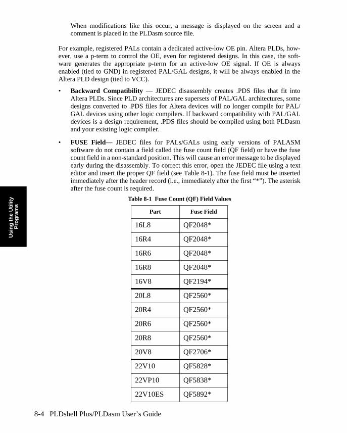
• FUSE Field— JEDEC files for PALs/GALs using early versions of PALASMsoftware do not contain a field called the fuse count field (QF field) or have the fusecount field in a non-standard position. This will cause an error message to be displayedearly during the disassembly. To correct this error, open the JEDEC file using a texteditor and insert the proper QF field (see Table 8-1). The fuse field must be insertedimmediately after the header record (i.e., immediately after the first “*”). The asteriskafter the fuse count is required.
Table 8-1 Fuse Count (QF) Field Values
Part Fuse Field
16L8 QF2048*
16R4 QF2048*
16R6 QF2048*
16R8 QF2048*
16V8 QF2194*
20L8 QF2560*
20R4 QF2560*
20R6 QF2560*
20R8 QF2560*
20V8 QF2706*
22V10 QF5828*
22VP10 QF5838*
22V10ES QF5892*

Usi
ng
th
e U
tilit
yP
rog
ram
s
PLDshell Plus/PLDasm User’s Guide 8-5
JEDEC Conversion
PLDshell Plus provides the capability to convert existing JEDEC files for common PALs/GALs into JEDEC files for Altera PLDs. A PLDasm source file is generated as a part ofthe conversion process. (JEDEC conversion consists of disassembly followedautomatically by compilation.)
The options available on the Convert JEDEC sub-menu are as follows:
Input Filename — Displays a list of JEDEC files to convert. The default extensionis .JED.
Source Device — Sets the source device to be used. Pressing the <Space> keydisplays a list of devices. When the source device has been selected, the target Alteradevice is automatically selected and displayed on the right.
Package Type — Sets the package type. Pressing the <Space> key displays a list ofpackage types for the device selected in the Source Device field.
Output Filename — Displays the output filename that will be created duringconversion. The default name is the target device name with a .JED extension.
Figure 8-3, JEDEC Conversion Messages, shows the messages displayed during JEDECconversion process. These messages were generated while converting the fileEX20V8.JED in your installation directory. This design uses all available inputs andoutputs.
Figure 8-3 JEDEC Conversion Messages
Running Conversion..INFO JDBMAC: 20V8 -> EP224 Disassembly in progressProcessing Macrocell [1]Processing Macrocell [2]Processing Macrocell [3]Processing Macrocell [4]Processing Macrocell [5]Processing Macrocell [6]Processing Macrocell [7]Processing Macrocell [8]INFO JDBMAC: JEDEC Disassembly Successfully Completed.INFO PARPDS: Parsing file: EP224.pdsINFO PARPDS: File parsed correctly.INFO PARPDS: Equation Expansion Complete.INFO FIT: Design compiled into EP224.INFO ASM: JEDEC file Assembled.
Conversion Successfully Completed.
Press ENTER to Continue...
Usi
ng
th
e U
tilit
y P
rog
ram
s
8-6 PLDshell Plus/PLDasm User’s Guide
Conversion Notes
The following notes apply to JEDEC conversion.
For all designs:
• I/O Names — During generation of a PLDasm source file, PLDshell Plus createssignal names based on the pin to which signals are mapped, e.g., “in8” means “inputpin 8”, “io13” means “I/O pin 13”, etc. You may wish to edit the resulting PLDasmsource file to change the signal names, then recompile the file.
• Turbo Bit(s)— Most Altera PLDs contain one or more Turbo Bits that optimizedevice performance for speed or power savings. The default state of the Turbo Bitsduring compilation is ON, which optimizes device performance for speed. If you wishto optimize a device for power savings, you must edit the resulting PLDasm source fileto specify TURBO=OFF, then recompile the source file using the Compile/Sim Menu.(The erased state of Altera PLDs is TURBO=OFF.)
For PAL/GAL Designs:
• PLCC Pinouts — Different pinouts have been adopted for PLCC devices by somePAL/GAL manufacturers. PLDshell Plus normalizes these different pinouts to thestandard pinout supported by Altera’s PLCC packages. Please note this possible pinoutdifference when converting designs from PAL/GAL JEDEC files.
• OE Inversions — In some cases, modifications are performed during disassembly toensure that the final design performs in the same way as the original design. OEinversion is performed automatically; you do not need to make this change yourself.When modifications like this occur, a message is displayed on the screen and acomment is placed in the PLDasm source file.
For example, registered PALs/GALs contain a dedicated active-low OE pin. AlteraPLDs, however, use a p-term to control the OE, even for registered designs. In this case,the software generates the appropriate p-term for an active-low OE signal. If OE is al-ways enabled (tied to GND) in registered PAL/GAL designs, it will be always enabled inthe Altera PLD design (tied to VCC).
• Backward Compatibility — JEDEC conversion creates .PDS and .JED files forAltera PLDs. Since PLD architectures are supersets of PAL/GAL architectures, somedesigns converted to .PDS files for Altera devices will no longer compile for PAL/GAL devices using other logic compilers. If backward compatibility with PAL/GALdevices is a design requirement, .PDS files should be compiled using both PLDasmand your existing logic compiler.
• FUSE field — JEDEC files for PALs/GALs using earlier versions of PALASMsoftware do not contain a field called the fuse count field (QF field) or have the fusecount field in a non-standard position. This will cause an error message to be displayedearly during the disassembly. To correct this error, open the JEDEC file using a texteditor and insert the proper QF field (see Table 8-1). The fuse field must be inserted

Usi
ng
th
e U
tilit
yP
rog
ram
s
immediately after the header record (i.e., immediately after the first “*”). The asterisk
PLDshell Plus/PLDasm User’s Guide 8-7
after the fuse count is required.
• Compile Options __ During JEDEC conversion, the PLDasm compiler is run withExpand Equations = Yes, Minimize = No, and Automatic Inversion = No. If you wantto compile with different options, recompile the intermediate .PDS file from theCompile/Sim Menu.

Usi
ng
th
e U
tilit
y P
rog
ram
s
8-8 PLDshell Plus/PLDasm User’s Guide
Translation
PLDshell Plus provides the capability of translating .ADF source files (originally writtenfor A+PLUS) or .SMF files into .PDS source files that can be compiled by PLDasm. Figure8-4 shows translation flow.
Figure 8-4 .SMF/.ADF Translation Flow
The options on the Translate sub-menu are as follows:
Input Filename — Displays a list of .ADF/.SMF files to be translated. The input filename can have any legal base name, but must have an .ADF or .SMF extension. Thedefault extension is .ADF; for .SMF files, you must type in the .SMF extension.
Output Filename — Displays the filename selected in the Input Filename field butwith a .PDS extension.
Translation Notes
The following notes apply to .ADF/.SMF -to- .PDS translation:
• During translation, state machines and truth tables are converted to Boolean equations.Thus, the .PDS source file generated by the translation utility will not contain statemachine and truth table syntax. The original state names and truth table names,however, are preserved in the Boolean equations.
• Macro calls in .ADF/.SMF designs are expanded into their Boolean equationimplementations during translation. The original macros appear in the .PDS file ascomments to help in tracing the translation process. The original signal names arepreserved.
• Comments in the .ADF/.SMF input files are not translated.
• If not specified in the .ADF/.SMF file, TURBO=ON is set in the .PDS options section.This is a change from A+PLUS, where the default was TURBO=OFF if the state of theTurbo Bit was not specified.
.SMFFile
.ADFFile
.PDSFile
TranslateISTATE

Usi
ng
th
e U
tilit
yP
rog
ram
s
PLDshell Plus/PLDasm User’s Guide 8-9
Merge
The Merge Utility allows you to merge from two to sixteen .PDS files into a single .PDSfile that can then be compiled or estimated. This section describes the methodology and amerge design example.
Methodology
The recommendations for an easy merge are simple: modular design and consistent signalnames.
Modular Design
Merge creates a high-level design that connects designs contained in separate .PDS files.To perform a merge, you specify the low-level files and the connectivity between them.
Break the higher-level designs into smaller functional blocks. (See Chapter 7 for moreinformation on modular design.)
Consistent Signal Names
Use a naming convention to make project management and maintenance easier. Formerging designs, consistent signal names allow you to try out several merge possibilitieswithout having to resolve signal names for each case. This is discussed in detail later in thischapter.
NOTE:
The timings of your original designs may not be preserved in yourmerged file.
Usi
ng
th
e U
tilit
y P
rog
ram
s
8-10 PLDshell Plus/PLDasm User’s Guide
Merge Example
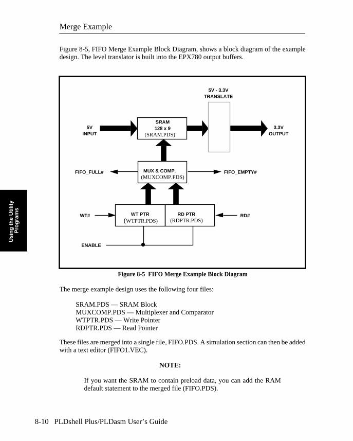
Figure 8-5, FIFO Merge Example Block Diagram, shows a block diagram of the exampledesign. The level translator is built into the EPX780 output buffers.
Figure 8-5 FIFO Merge Example Block Diagram
The merge example design uses the following four files:
SRAM.PDS — SRAM BlockMUXCOMP.PDS — Multiplexer and ComparatorWTPTR.PDS — Write PointerRDPTR.PDS — Read Pointer
These files are merged into a single file, FIFO.PDS. A simulation section can then be addedwith a text editor (FIFO1.VEC).
NOTE:
If you want the SRAM to contain preload data, you can add the RAMdefault statement to the merged file (FIFO.PDS).
SRAM128 x 9
MUX & COMP.
WT PTR RD PTR
FIFO_FULL# FIFO_EMPTY#
WT# RD#
ENABLE
5VINPUT
3.3VOUTPUT
5V - 3.3VTRANSLATE
(WTPTR.PDS) (RDPTR.PDS)
(MUXCOMP.PDS)
(SRAM.PDS)

Usi
ng
th
e U
tilit
yP
rog
ram
s
The files listed above are located in the installation directory for PLDshell Plus. Also, a file
PLDshell Plus/PLDasm User’s Guide 8-11
called FIFO1.PDS is in the same directory if you want to skip over the exercise and go rightto the results.
Accessing Merge
To select Merge, open the Utilities Menu, select Merge with the mouse or press the <M>key then <Enter>.
Adding Files to the Merge List
When the initial Merge screen is displayed, select Add. The screen shown in Figure 8-6will be displayed.
Figure 8-6 Add Screen with File List
Select each of the following four files, one at a time (if you use the sequence indicated, allscreens will match the figures exactly; choosing a different order will change the order ofsignals on the screens, but overall the information will be the same):
SRAM.PDSMUXCOMP.PDSWTPTR.PDSRDPTR.PDS
Usi
ng
th
e U
tilit
y P
rog
ram
s
When all four files have been added to the Merge List, the filenames will appear in that list.
8-12 PLDshell Plus/PLDasm User’s Guide
Select Accept.
NOTE:
If you inadvertently select the Cancel button, the Utilities Menu willappear.
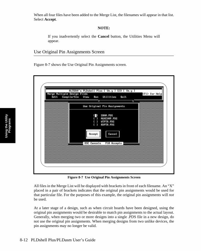
Use Original Pin Assignments Screen
Figure 8-7 shows the Use Original Pin Assignments screen.
Figure 8-7 Use Original Pin Assignments Screen
All files in the Merge List will be displayed with brackets in front of each filename. An “X”placed in a pair of brackets indicates that the original pin assignments would be used forthat particular file. For the purposes of this example, the original pin assignments will notbe used.
At a later stage of a design, such as when circuit boards have been designed, using theoriginal pin assignments would be desirable to match pin assignments to the actual layout.Generally, when merging two or more designs into a single .PDS file in a new design, donot use the original pin assignments. When merging designs from two unlike devices, thepin assignments may no longer be valid.

Usi
ng
th
e U
tilit
yP
rog
ram
s
Select
Accept
. This will display the Resolve I/O Signal Names/Types screen.
PLDshell Plus/PLDasm User’s Guide 8-13
NOTE:
If you select Cancel by mistake, the initial Merge screen will bedisplayed with the four files listed. You will need to select Accept to re-display this screen.
Resolve I/O Signal Names/Types Screen
Figure 8-8 Resolve I/O Signal Names/Types Screen
Note that the signal names are in alphabetical order. Where duplicate names exist (becausethey are used in more than one file, the signal associated with the first file selected is shownfirst). Merging assumes that all signals with the same name are to be connected together.
In this design example, you do not need to edit any of the fields. But to illustrate how tochange signals, change all MUXCOMP address outputs (A0 though A6) to “Buried” andclick on each “Output” so the label changes to “Buried.” Signal names and PinAssignments are changed by clicking on the respective field and entering text.
Select Accept. The next screen, Merge Design Files, will be displayed.
NOTE:
If you select Cancel by mistake, the initial Merge screen will bedisplayed with the four files listed. You will need to select Accept againto re-display this screen.

Usi
ng
th
e U
tilit
y P
rog
ram
s
8-14 PLDshell Plus/PLDasm User’s Guide
Merge Design Files Screen
Figure 8-9 shows the Merge Design Files screen. This screen contains two fields and theAccept and Cancel buttons:
Figure 8-9 Merge Design Files Screen
In the Output Filename field, type FIFO and press <Enter>.
Double click in the Target Device field and select the EPX780LC84 device (84-pin versionof the EPX780 FPGA).
When the correct Output Filename and Target Device have been entered, select Accept.
The message “Design Merge Successful!” will be displayed when the merge is completed.A new .PDS file has been created with the name FIFO.PDS. This file contains the input andoutput pin declarations together with module calls to the four .PDS files that make up thedesign. If you wish, you can view FIFO.PDS to see how the merge was accomplished.
Estimating and Simulating a Design
After you merge a design, perform an estimation to get a list of possible target devices. Ifyou know the device you want to use, select the device and compile the merged design.

Usi
ng
th
e U
tilit
yP
rog
ram
s
Use your text editor to append FIFO1.VEC to the end of FIFO.PDS. Select the Compile/
PLDshell Plus/PLDasm User’s Guide 8-15
Sim Menu. The merged file name, FIFO.PDS, will be displayed in the Source Filenamefield.
Double click in the Processing field. Select Estimate Then Simulate.
Click on the Compile Options button. Set the Auto Display Report to “Yes.” Select theAccept button.
The Compile/Sim Menu will again be displayed. Select the Accept button.
The Estimator and Simulator will begin processing. Figure 8-10, Estimator/SimulatorProcessing Screen, shows the screen display of this process.
Figure 8-10 Estimator/Simulator Processing Screen
INFO PARPDS: Parsing file: fifo.pds.INFO PDSTODDB: Expanding module reference in file: sram.pds.INFO PDSTODDB: Expanding module reference in file: muxcomp.pds.INFO PDSTODDB: Expanding module reference in file: wtptr.pds.INFO PDSTODDB: Expanding module reference in file: rdptr.pds.INFO PARPDS: File parsed correctly.INFO PARPDS: Equation expansion complete.INFO MIN: Espresso II-mv Copyright 1985 U.C. Berkeley RegentsINFO MIN: 66 Equations MinimizedINFO pldpick: Performing estimation analysis on design fifo1.Estimation analysis completed successfully - 2 of 10 devices checked may potentially fit design.SENGN Release [ Vx.y ] SID [ Vx.y ]
INFO SIM: Library [ flipflop.mac ] Loaded!INFO SIM: Library [ primtive.mac ] Loaded!
INFO SIM: Simulating file: fifo1.sim.INFO SIM: Vectors Generated - ( 10 )INFO SIM: Vectors Generated - ( 20 )INFO SIM: Vectors Generated - ( 30 )INFO SIM: Vectors Generated - ( 40 )INFO SIM: Vectors Generated - ( 50 )INFO SIM: Vectors Generated - ( 60 )INFO SIM: Vectors Generated - ( 70 )INFO SIM: Vectors Generated - ( 80 )INFO SIM: Total Vectors Generated - ( 85 )

Usi
ng
th
e U
tilit
y P
rog
ram
s
8-16 PLDshell Plus/PLDasm User’s Guide
Estimator Report
When processing is complete, press <Enter> to display the Estimator Report. This reportconsists of two parts: the Estimator Report section (shown in Figure 8-11) and a listing ofthe merged .PDS file that was estimated (not shown).
To view the simulation waveforms, use the Vector/Waveform Files option of the ViewMenu.
Figure 8-11 Estimator Report Example
pldpick [ Vx.y ] SID [ Vx.y ]DEVICE ESTIMATION REPORT FOR <fifo1>
*** DESIGN STATISTICS *** Inputs ........... 14 Outputs .......... 25 Active Pins (in+out) .... 39
Combinatorial.... 8 D flip-flops .... 19 T flip-flops .... 0 J/K (emulation) ... 0 Total Macrocells ............ 27 Buried Macrocells ... 11
Largest Product Term ... 10
SRAM Blocks ............ 1
DEVICE LISTED IN DESIGN: EPX780LC84 STATUS: OK
ACTIVE TOTAL TOTALPINS MCELLS PTERMS DEVICE
————- ————- ————- ————-EPX780LC84 39/62 27/80 25% 41%
*** POTENTIAL DEVICES THAT MAY FIT fifo ***
ACTIVE TOTAL TOTAL PINS MCELLS PTERMS DEVICE ————- ————— ———- ————-
EPX780LC84 39/62 27/80 25% 41% EPX780QC132 39/104 27/80 25% 35%
*** DEVICES REJECTED FOR fifo1 ***EP220 Not enough input+output pins for this designEP224 Not enough input+output pins for this design
EP22V10 Not enough input+output pins for this designEP610 Not enough input+output pins for this designEP910 Not enough input+output pins for this designEP312 Not enough input+output pins for this designEP324 Not enough input+output pins for this design

Des
ign
Ch
eckl
ist
PLDshell Plus/PLDasm User’s Guide 9-1
Chapter 9 — Design Checklist
This chapter provides a checklist for designers using Altera PLDs supported by PLDshellPlus. The term PLD is used in this Chapter to refer to any sort of Programmable LogicDevice, from either the Classic or FLEXlogic Families.
1. Check Report File?
2. Check Simulation Results?
3. Device Window Covered?
4. Unused Inputs and I/Os Grounded?
5. Turbo Bit On or Off?
6. Device Programmed Properly?
7. Adequate Decoupling on Vcc, Vcco, and Vpp?
8. Good Ground Plane?
9. Inputs Active Before Power-up?
10. Operating Conditions Within Specification?
11. Good Connection at Leads?
12. Second Opinion?
Design Checklist
1. Check Report File?
Check the Report File (.RPT) to see if the compiled logic reflects the original design.Certain compile options may change how a design is processed. These changes willshow up in the report file. Double-check the I/O architecture options, and ensure thatthe product terms for the equations or state machines are correct.
2. Check Simulation Results?
Check the simulation results (.HST or .TRF) to ensure that the logic compiled for thedesign simulated correctly under the conditions you specified. A simulation sectionis an easy first check for state machines or truth tables being specified correctly. Statemachine transitions or conditions can often be mislabeled, and the simulation canquickly verify this.

Des
ign
Ch
eckl
ist
3. Device Window Covered?
9-2 PLDshell Plus/PLDasm User’s Guide
Some Altera PLDs are fabricated using a standard EPROM process. Light enteringthrough the window in CerDIP packages can disturb internal voltages and may resultin indeterminate behavior. Covering the window with a label or UV filter ensuresstable behavior.
4. Unused Inputs and I/Os Grounded?
Unused inputs on Altera’s PLDs supported by PLDshell Plus are connected to a logicarray, even when they are not used by the macrocells. When unused input pins arenot tied high or low, they can cause devices to draw more power than necessary. Toensure the low power consumption, unused inputs should always be tied high or low.
For unused I/O pins, follow the directions for each pin as shown in the Report file(.RPT). You may be instructed to tie a pin to GND or to leave it alone (RESERVED).
5. Turbo Bit On or Off?
Most Altera PLDs supported by PLDshell Plus contain a Turbo Bit that optimizesdevice operation for speed or power savings. When the Turbo Bit is ON, the devicewill always be active and will always run at full speed. When the Turbo Bit is OFF,the device will enter standby mode if transitions are not detected on the input or I/Opins for a period of time. When powering up from standby mode in response to thenext transition, an added delay is incurred.
Debugging problems can occur if a designer is expecting full-speed performance(assuming the Turbo Bit is ON) and the device responds more slowly (because theTurbo Bit is OFF). Designers should always know the state of the Turbo Bit fordevices in their design.
When the Turbo Bit is OFF, but the device is being clocked at higher frequencies, itwill never enter standby mode. Refer to the ‘Icc vs. Frequency Graph’ in the devicedata sheet to determine the frequency range where the device will enter standbymode.
6. Device Programmed Properly?
Debugging problems can occur if a PLD is programmed with the wrong JEDEC file,or if the EPROM bits in a device are not fully programmed. When experiencingproblems with a design, check the following:
a. Verify the contents of the device against the original JEDEC file to make surethe correct design has been programmed into the device.
b.Program a second device using the same JEDEC file to see if it exhibits the samebehavior.
c. Verify the device on a second programmer to catch possible programmerproblems.
d. Is the Vpp signal connected correctly, decoupled and active at the proper timefor programming? Is the voltage at the specified datasheet level?
Des
ign
Ch
eckl
ist
7. Adequate Decoupling on Vcc, Vcco, and Vpp?
PLDshell Plus/PLDasm User’s Guide 9-3
Good decoupling practices should be followed for all designs using an Altera PLD(s).This will also help minimize any system noise, especially in higher-speed designs.Like most other devices PLDs can operate indeterminately when inputs are drivenpast the specified input threshold levels by noisy signals.
8. Good Ground Plane?
A ground plane should be used for all designs using PLDs. This will help minimizethe impact of system noise, especially in higher-speed designs. Like most otherdevices, PLDs can operate indeterminately when inputs are driven past the specifiedinput threshold levels by noisy signals.
9. Inputs Active Before Power-up?
Architecture bits in Altera PLDs supported by PLDshell Plus are loaded duringdevice power-up. During power-up, devices are not guaranteed to respond to activeinputs until after the specified power-up time. Refer to the power-up specification foreach device data sheet in the current Altera Data Book for details.
10. Operating Conditions Within Specification?
Altera PLDs are specified to operate within certain voltage and temperatureguidelines. If you are experiencing problems in a design, make sure that the systemenvironment (voltage and temperature) does not exceed the published specificationsfor the device.
11. Good Connection at Leads?
Make sure that all leads on Altera PLDs have good connections to the printed circuitboard or socket. Check for bent pins and solder bridges at the device and socketjunctions.
12. Second Opinion?
Designers are sometimes so close to a design that they overlook a relatively simpleproblem. It often helps to have a second designer spend a few minutes looking overthe design.

Des
ign
Ch
eckl
ist
9-4 PLDshell Plus/PLDasm User’s Guide

Sam
ple
Des
ign
s
PLDshell Plus/PLDasm User’s Guide 10-1
Chapter 10 — Sample Designs
Table 10-1 lists and summarizes sample designs that are useful in learning to design withPLDasm and the Altera PLDs supported by PLDshell Plus. All examples are included withPLDshell Plus in your installation directory. Some of these files are used as illustrations inthis manual.
Table 10-1 Example Filenames
Filename Description
File/Language Examples
TEMPLATE.PDS Template file containing blank fields and majorkeywords. Can be used to get a design started.This is a reference file only, not a working design.
SUMMARY.PDS Summary file showing examples of mainPLDasm syntax elements in a meaningful context.This is a quick reference file only, not a workingdesign.
Boolean Equations
4COUNT.PDS 4-bit synchronous counter in Boolean equations.Target device is an EP224. Illustrates basicregistered circuit design using Boolean equations.
4ERROR.PDS Same design as 4COUNT.PDS, but with anintentional error in the QA equation. Targetdevice is an EP224. Used to illustrate the on-lineerror help feature. See “Getting Started.”
PS2POS.PDS Programmable Option Select for PS/2 Adaptorcard in Boolean equations. Target device is anEP312.
CASCADE.PDS Large XOR function in Boolean equations. Targetdevice is an EP220. Illustrates how to distributelarge equations across macrocells to help fitdesigns.
16COUNT.PDS 16-bit binary counter in Boolean Equations.Target device is an EP910.
24COUNT.PDS 24-bit binary counter in Boolean Equations.Target device is an EP910. Illustrates use ofToggle flip-flops to simplify counter design.
Truth Tables
7SEG.PDS 7-segment decoder in Truth Table format. Targetdevice is an EP220. Illustrates Truth Table use fora simple combinatorial design.

Sam
ple
Des
ign
s
10-2 PLDshell Plus/PLDasm User’s Guide
Table 10-1 Example Filenames (Continued)
Filename Description
TCOUNT.PDS Counter implemented in Truth Table format andconverted to T-type flip-flops. Target device is anEP610. Illustrates how to use Truth Tables to im-plement counters.
State Machine Designs
2BIT.PDS 2-bit Up/Down Counter in State Machine format.Target device is an EP220. Illustrates use of StateMachine syntax in a simple design.
BUSCON1.PDS Simple Bus Controller circuit in State Machineformat. Target device is an EP224. IllustratesState Machine format for a simple design.
DOUBLCNT.PDS Two 4-bit counters, one synchronous, one asyn-chronous in State Machine format. Target deviceis an EP610. Illustrates use of State Machine syn-tax in a more complex design. Also illustratesasynchronous clocking of state machines.
EXMEALY1.PDS Mealy State Machine example in State Machineformat. Target device is an EP224. Used to illus-trate Mealy outputs in a state machine.
Application Examples (Mixed Format)
UPDOWN.PDS Up/down counter in State Machine format andBoolean equations. Device-independent design.Can be fitted to a variety of devices. Used to illus-trate the differences between device-independentand device-specific design.
STATEDEC.PDS State machine feeding a decoder in State Machineformat and Boolean equations. Target device is anEP600.
MEMCONT.PDS Shared memory controller for EISA add-in cardin State Machine format and Boolean equations.Target device is an EP610.
PULSE1.PDS Pulse generator examples in State Machine for-mat and Boolean equations. Target device is anEP312.
EX16R6.JED JEDEC file for a 16R6 design. Used to illustrateJEDEC disassembly/conversion to Altera PLDs.Target device is an EP220.
Disassembly/Conversion Examples
EX20L8.JED JEDEC file for a 20L8 design. Used to illustrateJEDEC disassembly/conversion to Altera PLDs.Target device is an EP224.

Sam
ple
Des
ign
s
Table 10-1 Example Filenames (Continued)
PLDshell Plus/PLDasm User’s Guide 10-3
EX20V8.JED JEDEC file for a 20V8 design. Used to illustrateJEDEC disassembly/conversion to Altera PLDs.Target device is an EP224.
.ADF/.SMF Translation Examples
SAMP1.ADF Sample 4-bit store and increment circuit writtenin .ADF format. Target device is an EP312. Usedto illustrate the .ADF-to-.PDS translation utility.
MANYMACH.SMF Multiple state machine file in .SMF format. Tar-get device is an EP312. Used to illustrate the.SMF-to-.PDS translation utility.
MACFILE.SMF State machine and TTL macro circuit in .SMF for-mat. Target device is an EP600. Used to illustratethe .SMF-to-.PDS translation utility.
EPX780 Design Examples
BYTEMAP1.PDS A sample design for mapping 32-bit CPU data in8-bit blocks using the EPX780.
SRAM.PDSMUXCOMP.PDSWTPTR.PDSRDPTR.PDSFIFO1.VECFIFO1.PDS
Four files that can be merged into a 128x9-bitwide FIFO. RDPTR = Read Pointer, WTPTR =Write Pointer, MUXCOMP = Multiplexer/Com-parator, SRAM = SRAM Definition. FIFO1.VECis a simulation vector file that can be appended tothe merged design for simulation. FIFO1.PDS isalso installed to show the final merged design.
3BIT.PDS1OF8.PDSWIGGLE.VEC
Two files that can be merged into a simple patterngenerator. 3BIT = 3-bit state machine, 1OF8 = 1of 8 decoder. WIGGLE.VEC is a simulation vec-tor file that can be appended to the merged designfor simulation. WIGGLE.PDS is also installed toshow the final merged design.
80TCNT.PDS 80-bit counter using Toggle flip-flops.
PCIARB1.PDS PCI bus arbiter design using a fixed-priority arbi-tration supporting 10 masters.
2BXOR.PDS2BCMPR.PDSHIGATE1.PDSHIGATE2.PDS
Example files for illustrating modular design syn-tax. HIGATE1.PDS calls 2BCMPR.PDS, whichin turn calls 2BXOR.PDS. HIGATE2.PDS com-bines the same functionality into a single sourcefile.
PATGEN1.PDS Serial pattern generator that stores a default pat-tern in SRAM. Consecutively reads 10 bits ofdata from SRAM, serializes it, and shifts the dataout.

Sam
ple
Des
ign
s
10-4 PLDshell Plus/PLDasm User’s Guide
Language Summary
PL
Dsh
ell M
od
el
Pro
gra
m
PLDshell Plus/PLDasm User’s Guide A-1
Appendix A — PLDshell Model Program
This appendix lists a model PLDshell program. It shows the file, SUMMARY.PDS, whichillustrates many of the PDS language elements. SUMMARY.PDS is a reference file only,not a working design.
For quick reference, more language information is provided in Appendix E.
Title PLDasm Language Summary (summary.pds)Pattern <<pattern label>>Revision <<rev. number>>Author <<your name>>Company <<your company>>Date <<current date>>
; Comments up to the first CHIP, OPTIONS or DEFMOD keyword are included in; the Header for the Report and JEDEC file for a design.
; Optional Module definitionsDEFMOD <module name> ( <argument list> )
CHIP <module name> ALTERA_ARCH
PIN <argument list name>NODE <any buried pin>
; valid PDS syntax that defines a logic function.; EQUATIONS/STATE/MODULE/T_TAB Sections allowed
ENDMOD;--------------------------------------------------------------------------
OPTIONS ; Must be before CHIP keyword section
; Not all options are available for every device.; The Default value is the first value in each options list
TURBO = [ON|OFF] ; sets TURBO bit in device SECURITY = [OFF|ON] ; sets SECURITY bit(s) in device
EXPAND = [ON|OFF] ; Reduce to 2-level SOP equations INVERSION = [ON|OFF] ; Allow left-hand side to be inverted DT_SYNTHESIS = [ON|OFF] ; D or T Flip-flops; FLEXlogic devices only MINIMIZATION = [ON|OFF] ; Controls Espresso algorithm
; Options that only work with the FLEXlogic device fitter DRIVE_LEVEL = [5VOLT|3VOLT] ; default I/O voltage level
FITTER_PINS = [KEEP|TRY|IGNORE] ; What to do with pins in .PDS file FITTER_PREV_PINS = [ON|OFF] ; use .PIN file first, if it exists FITTER_ALGORITHM = [NORMAL|COMPLETE] ; Use NORMAL or exhaustive fitting
; algorithms
; When using the PLDshell GUI interface, all of these options; can be overridden by the Compile->Compile Options Menu,

PL
Dsh
ell M
od
elP
rog
ram
; except for TURBO, SECURITY and DRIVE_LEVEL.
A-2 PLDshell Plus/PLDasm User’s Guide
;--------------------------------------------------------------------------; Design Name PartnameCHIP summary EPxxxx
;; For partname information, see Table 1-1 in the PLDshell Plus Manual; and the current Altera Data Book.;
; PINLIST
PIN 1 CLOCK
PIN 1 DCLOCK DELAYCLK ; uses delayed clock
PIN UPDOWN ; undefined pin assignmentPIN /CLEAR ; active-low signal
PIN 2 I1 ; Direct Inputs, with pin assignmentsPIN 3 I2PIN 4 I3PIN 5 I4
PIN [2:5] I[1:4] ; with vector notation
PIN[0:3] D[0:3] ; vector notation
NODE 32 Q0 ; buried state variables for a state machineNODE Q1 ; unassignedNODE Q2NODE IO27 Q3 ; assigned to a macrocell
; -- Output Types -- ; Combinatorial Output, I/O Feedback PIN O1 COMB PINFBK
; Combinatorial Output, MC Feedback, 5VOLT output PIN O2 COMB CMBFBK 5VOLT
; Combinatorial Output, Reg Feedback (EP22V10E and EPX7xx only) PIN O3 COMB REGFBK
; Buried Combinatorial Macrocell NODE O4 CMBFBK BURIED
; Registered Output, I/O Feedback, with 3.3 VOLT output PIN O5 REG PINFBK 3VOLT
; Registered Output, MC Feedback PIN O6 REG REGFBK

Language Summary
PL
Dsh
ell M
od
el
Pro
gra
m
; Buried Register
PLDshell Plus/PLDasm User’s Guide A-3
PIN O7 REGFBK BURIED ; Or the equivalent is to use the NODE keyword NODE O7 REG
; A 5 volt Open Drain Output PIN 10 5VOLT OPEN_DRAIN
; T Feedback Combinatorial Output PIN cout_t TREGFBK
; JK Feedback Combinatorial Output PIN cout_t JKFBK
; SR Feedback Combinatorial Output PIN cout_sr SRFBK
; T Output Combinatorial Feedback PIN tout CMBFBK
; JK Output Combinatorial Feedback PIN jkout CMBFBK
; SR Output Combinatorial Feedback PIN srout CMBFBK
; -- Input Types -- ; Latched Input (EP312/EP324) PIN 5 LIN1 LATCHED
; Registered Input (EP312/EP324) PIN 6 RIN1 REG
; CMOS LEVEL INPUTS PIN 7 IN2 5VOLT CMOS_LEVEL
; TTL LEVEL INPUTS PIN 8 IN3 3VOLT TTL_LEVEL
; -- SRAM Types --
; Combinatorial SRAM output PIN BUFRAM[0:9] RAM
; Buried Combinatorial SRAM NODE ROMTAB[8:0] RAM
; Buried Registered (D) SRAM NODE MACHTAB[9:0] REG RAM
; -- String Substitutions throughout file --

PL
Dsh
ell M
od
elP
rog
ram
; These must appear after all Pin declarations
A-4 PLDshell Plus/PLDasm User’s Guide
STRING QADS ' (ADS * PCLK * /RESET) ' STRING RASON ' ((RAS0 + RAS1) * /IREADY) '
; Design Sections can appear in any order; but the Simulation; section must appear last;; [ STATE ] -- can have multiple state machines; [ EQUATIONS ] -- can have multipe equation sections; [ T_TAB ] -- can have multiple truth tables; [ MODULE ] -- can have multiple module calls; [ RAM_DEFAULTS ] -- can have multiple ram defaults;; [ SIMULATION ] -- only one simulation section allowed, must be last;; At least one STATE/EQUATIONS/T_TAB/MODULE section must appear.
; -- State Machine Format --STATE [MEALY_MACHINE|MOORE_MACHINE]
; 1 0 specifies output values on hold conditions OUTPUT_HOLD OUT1 /OUT2
; 0 1 X specifies default output values DEFAULT_OUTPUT /OUT1 OUT2 %OUT3
; branches for unresolved states DEFAULT_BRANCH S0 ; go to S0 DEFAULT_BRANCH HOLD_STATE ; stay in current state DEFAULT_BRANCH NEXT_STATE ; go to next state in assignments list
; State assignments, value of the machine variables for each state.; Gray code state assignments for a two-bit machine, S0-S3
S0 = /Q1 * /Q0 ; power-up state of Altera Device Registers S1 = /Q1 * Q0 S2 = Q1 * Q0 S3 = Q1 * /Q0
; Gray code state assignments for a three-bit machine, S0-S7
S0 = /Q2 * /Q1 * /Q0 ; power-up state of Altera Device Registers S1 = /Q2 * /Q1 * Q0 S2 = /Q2 * Q1 * Q0 S3 = /Q2 * Q1 * /Q0 S4 = Q2 * Q1 * /Q0 S5 = Q2 * Q1 * Q0 S6 = Q2 * /Q1 * Q0 S7 = Q2 * /Q1 * /Q0 ; state transitions
S0 := VCC -> S1 ; on next clock go to S1

Language Summary
PL
Dsh
ell M
od
el
Pro
gra
m
PLDshell Plus/PLDasm User’s Guide A-5
S1 := UP -> S2 + DOWN -> S4
; output transitions, MOORE; Moore outputs are default transitions (VCC) only
S1.OUTF := VCC -> LOCAL * /MEMORY * /INTACK ; registered S2.OUTF = VCC -> ASTRB ; combinatorial S3.OUTF = VCC -> ASTRB
; output transitions, MEALY; Mealy's may have conditions on the output transitions
S1.OUTF := DOWN -> LOCAL * /MEMORY * /INTACK ; registered + UP -> /LOCAL S2.OUTF = UP -> ASTRB ; combinatorial S3.OUTF = VCC -> ASTRB
; input conditions that determine state and output transitions CONDITIONS UP = UPDOWN * /CLEAR DOWN = /UPDOWN * /CLEAR ACTIVE = /EN + RDY
; Moore machines are level sensitive. The outputs do not change until; the next clock edge. Mealy machines can generate pulse signals.; The outputs may change before the next clock edge. See also the; examples in exmealy1.pds and pulse1.pds.
; -- Boolean Equations section --EQUATIONS
O1 = ... ; -- Combinatorial Output (COMBINATORIAL) O1 := ... ; -- Registered (D) Output (REGISTERED) O1.FB ; -- Feedback path from macrocell (REGFBK, CMBFBK)
O1.D := ... ; -- Registered (D) Output (REGISTERED) O1.T := ... ; -- Toggle (T) Output
O1.J := ... ; -- J/K Output (emulated J/K. Synchronized with .CLKF) O1.K := ...
O1.S := ... ; -- S/R Output (emulated J/K. Synchronized with .CLKF) O1.R := ...
; -- Control Signals -- O1.CLKF = CLOCK ; Register clock signal O1.ACLK = CLOCK * ENABLE ; Asynchronous clock signal, from pterm array
; See Device Descriptions Chapter in the PLDshell Plus Manual for ; specific device clocking options, and macrocell control signals.
O1.RSTF = CLEAR ; Register Clear signal
PL
Dsh
ell M
od
elP
rog
ram
A-6 PLDshell Plus/PLDasm User’s Guide
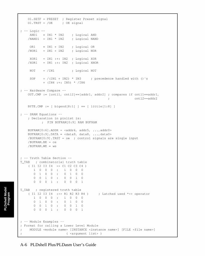
O1.SETF = PRESET ; Register Preset signal O1.TRST = /OE ; OE signal
; -- Logic -- AND1 = IN1 * IN2 ; Logical AND /NAND1 = IN1 * IN2 ; Logical NAND
OR1 = IN1 + IN2 ; Logical OR /NOR1 = IN1 + IN2 ; Logical NOR
XOR1 = IN1 :+: IN2 ; Logical XOR /XOR1 = IN1 :+: IN2 ; Logical XNOR
NOT = /IN1 ; Logical NOT
SOP = /(IN1 + IN2) * IN3 ; precedence handled with ()'s + (IN4 :+: IN5) * /IN6
; -- Hardware Compare -- OUT.CMP := [cntl1, cntl2]==[addr1, addr2] ; compares if cntl1==addr1, ; cntl2==addr2
BYTE.CMP := [ bigend[8:1] ] == [ little[1:8] ] ; -- SRAM Equations -- ; Declaration in pinlist is:
; PIN BUFRAM[0:9] RAM BUFRAM
BUFRAM[0:6].ADDR = <addr6, addr5, ...,addr0> BUFRAM[0:9].DATA = <data9, data8, ...,data0> /BUFRAM[0:9].TRST = oe ; control signals are single input /BUFRAM.BE = ce /BUFRAM.WE = we
; -- Truth Table Section --T_TAB ; combinatorial truth table ( I1 I2 I3 I4 >> C1 C2 C3 C4 ) 1 0 0 0 : 1 0 0 0 0 1 0 0 : 0 1 0 0 0 0 1 0 : 0 0 1 0 0 0 0 1 : 0 0 0 1
T_TAB ; registered truth table ( I1 I2 I3 I4 :>> R1 R2 R3 R4 ) ; Latched used *>> operator 1 0 0 0 : 1 0 0 0 0 1 0 0 : 0 1 0 0 0 0 1 0 : 0 0 1 0 0 0 0 1 : 0 0 0 1
; -- Module Examples -- ; Format for calling a Lower Level Module; MODULE <module name> [INSTANCE <instance name>] [FILE <file name>] ; ( <argument list> )
Language Summary
PL
Dsh
ell M
od
el
Pro
gra
m
PLDshell Plus/PLDasm User’s Guide A-7
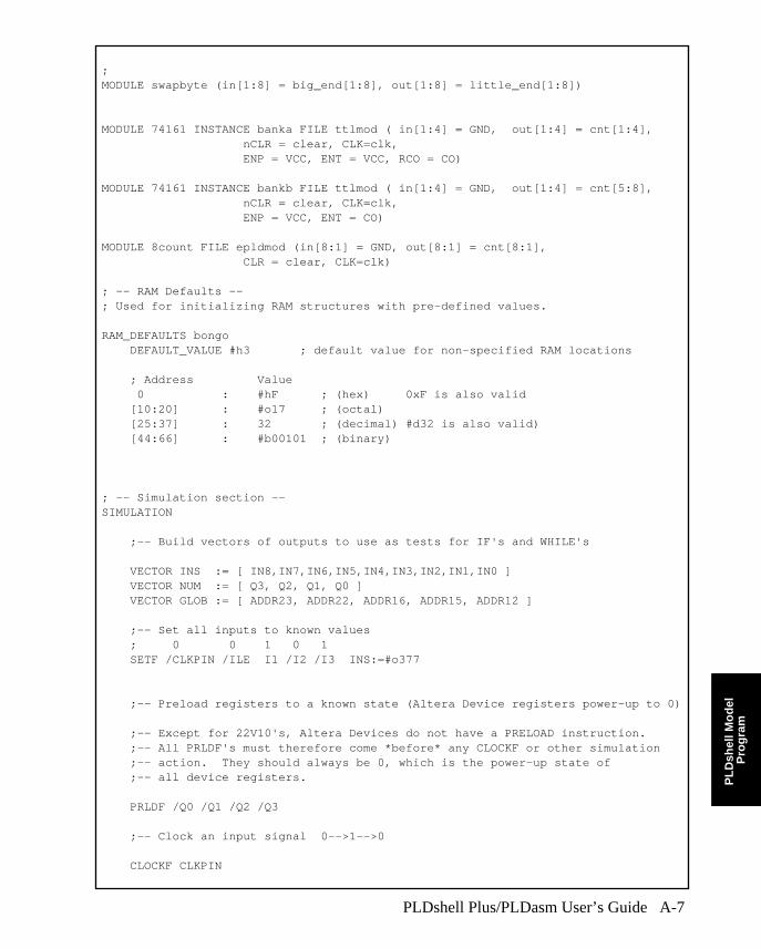
;MODULE swapbyte (in[1:8] = big_end[1:8], out[1:8] = little_end[1:8])
MODULE 74161 INSTANCE banka FILE ttlmod ( in[1:4] = GND, out[1:4] = cnt[1:4], nCLR = clear, CLK=clk, ENP = VCC, ENT = VCC, RCO = CO)
MODULE 74161 INSTANCE bankb FILE ttlmod ( in[1:4] = GND, out[1:4] = cnt[5:8], nCLR = clear, CLK=clk, ENP = VCC, ENT = CO)
MODULE 8count FILE epldmod (in[8:1] = GND, out[8:1] = cnt[8:1], CLR = clear, CLK=clk)
; -- RAM Defaults --; Used for initializing RAM structures with pre-defined values.
RAM_DEFAULTS bongo DEFAULT_VALUE #h3 ; default value for non-specified RAM locations ; Address Value 0 : #hF ; (hex) 0xF is also valid [10:20] : #o17 ; (octal) [25:37] : 32 ; (decimal) #d32 is also valid) [44:66] : #b00101 ; (binary)
; -- Simulation section --SIMULATION
;-- Build vectors of outputs to use as tests for IF's and WHILE's
VECTOR INS := [ IN8,IN7,IN6,IN5,IN4,IN3,IN2,IN1,IN0 ] VECTOR NUM := [ Q3, Q2, Q1, Q0 ] VECTOR GLOB := [ ADDR23, ADDR22, ADDR16, ADDR15, ADDR12 ]
;-- Set all inputs to known values ; 0 0 1 0 1 SETF /CLKPIN /ILE I1 /I2 /I3 INS:=#o377
;-- Preload registers to a known state (Altera Device registers power-up to 0)
;-- Except for 22V10's, Altera Devices do not have a PRELOAD instruction. ;-- All PRLDF's must therefore come *before* any CLOCKF or other simulation ;-- action. They should always be 0, which is the power-up state of ;-- all device registers.
PRLDF /Q0 /Q1 /Q2 /Q3
;-- Clock an input signal 0-->1-->0
CLOCKF CLKPIN

PL
Dsh
ell M
od
elP
rog
ram
A-8 PLDshell Plus/PLDasm User’s Guide
;-- CHECK output values, report any mismatches ; 1 0 0 0 1 1 CHECK O1 /O2 /O3 /O4 O5 O6 CHECK /AOK[15:0]
;-- FOR loop to count up 6 clocks
FOR j := 0 TO 5 DO BEGIN SETF INS := j CLOCKF CLK IF ( NUM == 4 ) ; when in state 4 BEGIN SETF /OE ; disable OE END END
;-- loop until OUTA and OUTB are both low
WHILE ( OUTA + OUTB ) DO BEGIN CLOCKF ACLK1 END
; end simulation

PL
Dsh
ell
Co
nfi
gu
rati
on
File
PLDshell Plus/PLDasm User’s Guide B-1
Appendix B — PLDshell Configuration File
This section describes the PLDSHELL.CFG configuration file used by PLDshell Plus/PLDasm. The configuration file is distributed with PLDshell Plus, and is copied to theinstall directory during installation. Figure B-1 shows the full format of the configurationfile. If the defaults are used, many entries will not be present until changes are made.
The following is a list of the supported variable assignments and a description of theirfunctions:
IPLSPATH Specifies directory path(s) to the PLDshell Plus andassociated files, which are usually in the samedirectory.
INCLUDE Specifies directory path to .DPP macro files.
PLD_MSG Specifies the file name of the message database file.PLDshell Plus messages are all contained in thisfile.
MPFFILE Specifies the name of the Master Parts File.
PLD_MLIB Specifies the macro libraries used during .SMF/.ADF translation. The default entries are TTL.LIBand EPLDMAC.LIB.
PARJKTERM Specifies the value which controls JK product termoptimization in the ADF parser. The larger thenumber, the larger the equation the parser willaccept for processing (and the longer the processingwill take). Valid values are decimal units (in productterms).
CMDSHELL Specifies the command shell program to run.
EDITOR Text editor for PLDshell Plus. Default is the DOSEDIT editor. Use the Utilities—Options submenu.
WORKDIR Specifies the default working directory. This optioncan be saved to the configuration file by selectingSave Options in the Options dialog.
HOTKEYS Allows selection of menus and submenus by usingthe first letter of the menu name. The first letter ishighlighted. Default is ON. Use the Utilities—Options submenu.

PL
Dsh
ell
Co
nfi
gu
rati
on
File
PRINTER Sets the printer port. The default is PRN. Use the
B-2 PLDshell Plus/PLDasm User’s Guide
Utilities-Options submenu.
PDSEXT Sets the file extension for .PDS files. The default is.PDS. Use the Utilities-Options submenu.
COMP_ERRFILE YESCOMP_RPTFILE YESCOMP_EXPANDEQN DefaultCOMP_MINIMIZE DefaultCOMP_AUTOINV Default
These are the Compiler Options, accessible throughthe Compile Options submenu. The default value isshown with each option.
COMP_FITMODE USE_PDS_DEFAULTS Controls how pin assignments are handled by the fitter. Other legal values are: KEEP_RPT_PINS, TRY_RPT_PINS, KEEP_PDS_PINS, TRY_PDS_PINS, IGNORE_PINS.
COMP_AUTORPT Automatically views the .RPT file (if generated)after compiling or the .EST file after estimating.Default is NO.
COMP_PROC Specifies the default processing option on theCompile/Sim Menu:
0 = Compile Then Simulate1 = Compile Only2 = Simulate Only3 = Estimate Only4 = Estimate Then Simulate
This option is set in the Compile/Sim Menu and canbe saved from the Compile Options submenu.
SIM_ASYNC NOSIM_THRESHOLD 32
These are the Simulator Options, accessible throughthe Simulation Options submenu. The default isshown with each option.
WAVE_PGLEN 66WAVE_VIEW GRAPHICALWAVE_PRINT PLAIN
These are the View Options, accessible through theView Menu. The default is shown with each option.The alternate entry for WAVE_VIEW isSTATETABLE. The alternate entry forWAVE_PRINT is EXTENDED.
PROGA-PROGX These are the Run Menu program fields, accessiblethrough the Run Menu.
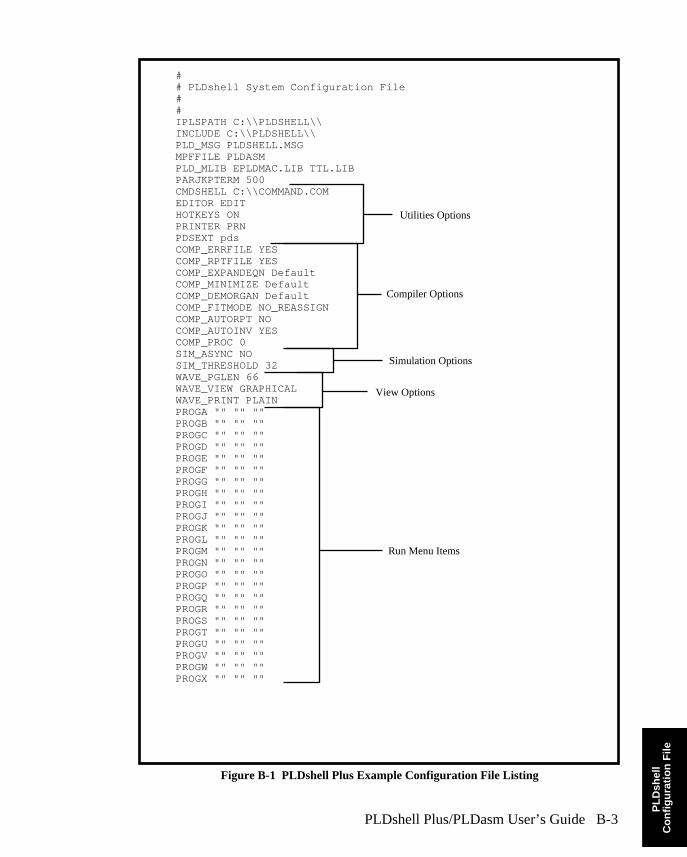
PL
Dsh
ell
Co
nfi
gu
rati
on
File
PLDshell Plus/PLDasm User’s Guide B-3
Figure B-1 PLDshell Plus Example Configuration File Listing
# # PLDshell System Configuration File # # IPLSPATH C:\\PLDSHELL\\INCLUDE C:\\PLDSHELL\\PLD_MSG PLDSHELL.MSGMPFFILE PLDASMPLD_MLIB EPLDMAC.LIB TTL.LIBPARJKPTERM 500CMDSHELL C:\\COMMAND.COMEDITOR EDITHOTKEYS ONPRINTER PRNPDSEXT pdsCOMP_ERRFILE YESCOMP_RPTFILE YESCOMP_EXPANDEQN DefaultCOMP_MINIMIZE DefaultCOMP_DEMORGAN DefaultCOMP_FITMODE NO_REASSIGNCOMP_AUTORPT NOCOMP_AUTOINV YESCOMP_PROC 0SIM_ASYNC NOSIM_THRESHOLD 32WAVE_PGLEN 66WAVE_VIEW GRAPHICALWAVE_PRINT PLAINPROGA "" "" ""PROGB "" "" ""PROGC "" "" ""PROGD "" "" ""PROGE "" "" ""PROGF "" "" ""PROGG "" "" ""PROGH "" "" ""PROGI "" "" ""PROGJ "" "" ""PROGK "" "" ""PROGL "" "" ""PROGM "" "" ""PROGN "" "" ""PROGO "" "" ""PROGP "" "" ""PROGQ "" "" ""PROGR "" "" ""PROGS "" "" ""PROGT "" "" ""PROGU "" "" ""PROGV "" "" ""PROGW "" "" ""PROGX "" "" ""
Utilities Options
Compiler Options
Simulation Options
View Options
Run Menu Items

PL
Dsh
ell
Co
nfi
gu
rati
on
File
B-4 PLDshell Plus/PLDasm User’s Guide
Co
mm
and
Lin
eIn
terf
ace
PLDshell Plus/PLDasm User’s Guide C-1
Appendix C — Command Line Interface
The following PLDshell/PLDasm program functions can be directly accessed from theDOS prompt:
CompilerDisassemblerConversionTranslationEstimator
This appendix describes the PLDasm command line interface for these functions.
Command Line Interface
The PLDasm command line syntax is as follows:
pldasm <action> [<options>] <files>
where action is one of the following:
COM[PILE]D[ISASSEMBLE]CON[VERT]T[RANSLATE]E[STIMATE]
The minimum number of characters for each action is that which identifies it as a uniqueaction (i.e., “D” for Disassemble, “CON” for Convert, etc.).
Command Line Help
PLDasm has a command line help feature that provides you with a description andexamples of the proper usage. To access the PLDasm help, type:
pldasm <action>
where <action> is one of the above listed actions.
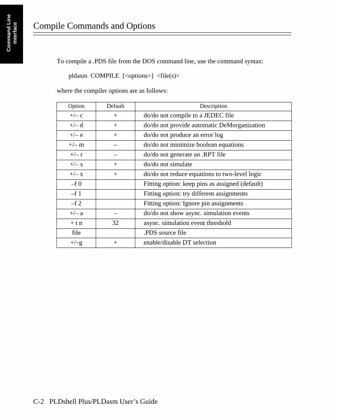
Co
mm
and
Lin
eIn
terf
ace
C-2 PLDshell Plus/PLDasm User’s Guide
Compile Commands and Options
To compile a .PDS file from the DOS command line, use the command syntax:
pldasm COMPILE [<options>] <file(s)>
where the compiler options are as follows:
Option Default Description
+/– c + do/do not compile to a JEDEC file
+/– d + do/do not provide automatic DeMorganization
+/– e + do/do not produce an error log
+/– m – do/do not minimize boolean equations
+/– r – do/do not generate an .RPT file
+/– s + do/do not simulate
+/– x + do/do not reduce equations to two-level logic
–f 0 Fitting option: keep pins as assigned (default)
–f 1 Fitting option: try different assignments
–f 2 Fitting option: Ignore pin assignments
+/– a – do/do not show async. simulation events
+ t n 32 async. simulation event threshold
file .PDS source file
+/–g + enable/disable DT selection

Co
mm
and
Lin
eIn
terf
ace
PLDshell Plus/PLDasm User’s Guide C-3
Compilation Examples
The following are examples of compiler operation from the DOS command line:
pldasm comp -sim -min 4count.pds
In this example, simulation and the minimizer are both turned off. No simulation file willbe created and p-term minimization will not be performed.
pldasm comp -comp +async +thres 55 count.pds
In this example, compilation is turned off, and a maximum of 55 asynchronous events willbe permitted/shown during each simulation step.

Co
mm
and
Lin
eIn
terf
ace
C-4 PLDshell Plus/PLDasm User’s Guide
Disassembler Commands and Options
To disassemble a JEDEC file from the DOS command line, use the following commandsyntax:
pldasm dis <part> <package> <file>
where:
<part> is any valid part recognized by PLDasm.
<package> is any valid package type: DIP, PLCC, PGA.
<file> is a JEDEC input file. The output file is the target Altera device name with a.JED extension.
Disassembly Example
pldasm DIS 16V8 PLCC UDCTR.JED
In this example, the <part> is a 16V8 in a PLCC package. The input file is UDCTR.JED.Note that the 16V8 JEDEC file will be disassembled into a .PDS file for the respectiveAltera PLD. The output filename is EP220.PDS. Table 1-2 lists all supported PLDs.

Co
mm
and
Lin
eIn
terf
ace
PLDshell Plus/PLDasm User’s Guide C-5
Conversion Commands and Options
Convert disassembles a JEDEC file for a PAL device, producing a PDS file, which is thencompiled to a JEDEC file for an Altera PLD supported by PLDshell. To convert a JEDECfile, use the following command syntax:
pldasm CONV <part> <package> {[<compiler_options>]} <file>
where:
<part> is any valid part recognized by PLDasm.
<package> is any valid package type: DIP, PLCC, PGA.
<compiler_options> are the same options as for the compiler (see “CompileCommands and Options”).
<file> is a JEDEC input file. The output file is the target Altera device name with a.JED extension.
Conversion Examples
pldasm CONV 20L8 DIP UDCNTR.JED
In this example, <part> is a 20L8 in a DIP package. The output file is EP224.JED.
pldasm CONV 20L8 DIP +min UDCTR.JED
In this example, <part> is a 20L8 in a DIP package. The compiler minimizer is turned on.The output file is EP224.JED.
Translation Commands and Options
Translate produces a .PDS source file from input files in another PLD language (.ADF/.SMF files). To use the translate command from the DOS command line, use the followingsyntax:
pldasm TRAN [-i file.in] [-o file.out]
where:
-i file.in is the input filename (optional)
-o file.out is the output filename (optional)

Co
mm
and
Lin
eIn
terf
ace
C-6 PLDshell Plus/PLDasm User’s Guide
Translation Examples
pldasm TRAN COUNTER.ADF
In this example, the input file COUNTER.ADF is translated into the output fileCONVERT.PDS.
pldasm TRAN -i COUNTER.ADF -o NEWCTR.PDS
In this example, the input file COUNTER.ADF is translated into the output fileNEWCTR.PDS.
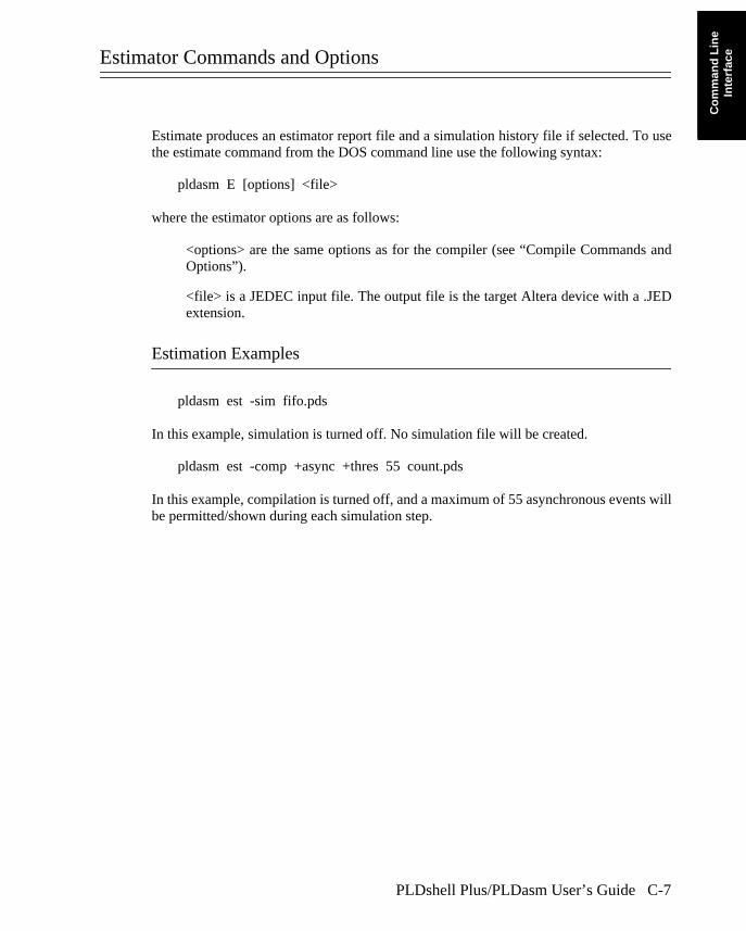
Co
mm
and
Lin
eIn
terf
ace
PLDshell Plus/PLDasm User’s Guide C-7
Estimator Commands and Options
Estimate produces an estimator report file and a simulation history file if selected. To usethe estimate command from the DOS command line use the following syntax:
pldasm E [options] <file>
where the estimator options are as follows:
<options> are the same options as for the compiler (see “Compile Commands andOptions”).
<file> is a JEDEC input file. The output file is the target Altera device with a .JEDextension.
Estimation Examples
pldasm est -sim fifo.pds
In this example, simulation is turned off. No simulation file will be created.
pldasm est -comp +async +thres 55 count.pds
In this example, compilation is turned off, and a maximum of 55 asynchronous events willbe permitted/shown during each simulation step.

Co
mm
and
Lin
eIn
terf
ace
C-8 PLDshell Plus/PLDasm User’s Guide

Err
or
Mes
sag
es
PLDshell Plus/PLDasm User’s Guide D-1
Appendix D — Error Messages
PLDASM Error Messages
ERROR E104: Occurs: No room left in memory for dynamic allocation.Action: Reduce memory usage by removing memory-resident programs and/or utilities.
Refer to your installation instruction guide and/or your system administrator forsuggestions.
ERROR E108:Occurs: An unsupported device name was used, and there is no JEDEC information.Action: Use a supported device name that can be compiled. Check the user manual.
ERROR E109:Occurs: The JEDEC Address File (JAF) for the specified target device is not found in the
present drive/path. It has the part name as its filename, followed by the .JAFextension, e.g., EP224.JAF.
Action: Recheck the configuration file path variable (IPLSPATH) to be sure that thecorrect directories are included. If the path is okay, then reload the software in casethe installed file has been corrupted.
ERROR E111:Occurs: Could not write to a file on disk.Action: Make sure the disk is not write-protected, and that there is adequate room on the
disk for the files. A file name may have been corrupted. In DOS, run the CHKDSKprogram.
ERROR E113:Occurs: Could not write to the JEDEC file on disk.Action: Make sure the disk is not write-protected, and that there is adequate room on the
disk for the files. A file name may have been corrupted. In DOS, run the CHKDSKprogram.
ERROR E114:Occurs: JEDEC Address File for the device contains more data than can fit in the allocated
memory space.Action: Reinstall software from distribution media. If the error persists, contact Altera
Applications at (800) 800-EPLD or (408) 894-7000 for assistance.
ERROR E115:Occurs: Data contained in .CHP file does not match expected data.Action: Run a disk diagnostic. If there are no problems, try rebooting the machine and
removing any TSR programs. If the error persists, reinstall the software.

Err
or
Mes
sag
es
ERROR E116:
D-2 PLDshell Plus/PLDasm User’s Guide
Occurs: An illegal JEDEC address was generated by the compiler.Action:
Step 1. Delete all temporary files on the disk. Run a disk diagnostic to make sureall files are not corrupted. Try to re-run the compiler.
Step 2. Gather all compiler input and output files in the design, and contactAltera Applications at (800) 800-EPLD or (408) 894-7000 for assistance.
ERROR E117:Occurs: An illegal device resource was generated by the compiler.Action:
Step 1. Delete all temporary files on the disk. Run a disk diagnostic to make sureall files are not corrupted. Try to re-run the compiler.
Step 2. Gather all compiler input and output files in the design, and contactAltera Applications at (800) 800-EPLD or (408) 894-7000 for assistance.
ERROR E118:Occurs: An illegal JEDEC equation was generated by the compiler.Action:
Step 1. Delete all temporary files on the disk. Run a disk diagnostic to make sureall files are not corrupted. Try to re-run the compiler.
Step 2. Gather all compiler input and output files in the design, and contactAltera Applications at (800) 800-EPLD or (408) 894-7000 for assistance.
ERROR E119:Occurs: An internal compiler data structure was corrupted in memory.Action:
Step 1. Delete all temporary files on the disk. Run a disk diagnostic to make sureall files are not corrupted. Then try to re-run the compiler.
Step 2. Check that the PATHs in the configuration file point to the correctdirectories for the product. Try to reinstall the software.
Step 3. Remove TSRs and other memory resident programs.Step 4. Gather all compiler input and output files in the design, and contact
Altera Applications at (800) 800-EPLD or (408) 894-7000 for assistance.
ERROR E120:Occurs: An illegal macrocell number was generated by the compiler.Action:
Step 1. Delete all temporary files on the disk. Run a disk diagnostic to make sureall files are not corrupted. Try to re-run the compiler.
Step 2. Gather all compiler input and output files in the design, and contactAltera Applications at (800) 800-EPLD or (408) 894-7000 for assistance.
ERROR E121:Occurs: An unsupported macrocell control has been used. (e.g., PRESET or CLEAR on an
EP224).Action: Remove the equations driving these controls or implement the control signal
synchronously rather than asynchronously. Check the report file to see if thedesign fit.
Err
or
Mes
sag
es
ERROR E122, E123:
PLDshell Plus/PLDasm User’s Guide D-3
Occurs: An internal compiler data structure was corrupted in memory.Action:
Step 1. Delete all temporary files on the disk. Run a disk diagnostic to make sureall files are not corrupted. Try to re-run the compiler.
Step 2. Gather all compiler input and output files in the design, and contactAltera Applications at (800) 800-EPLD or (408) 894-7000 for assistance.
ERROR E124:Occurs: More product terms are included in the equation than are supported in the device.Action: Reduce the number of product terms in the equation or use minimization. Look for
nested equations. It may be necessary to route part of the equation through anintermediate macrocell using NO-OUTPUT/COMBINATORIAL FEEDBACKor COMBINATORIAL OUTPUT/PIN FEEDBACK macrocell architectures.Consider using devices that support more p-terms.
ERROR E125:Occurs: The compiler generated allocation data for a device that does not have any.Action:
Step 1. Delete all temporary files on the disk. Run a disk diagnostic to make sureall files are not corrupted. Then try to re-run the compiler.
Step 2. Gather all compiler input and output files in the design, and contactAltera Applications at (800) 800-EPLD or (408) 894-7000 for assistance.
ERROR E126:Occurs: An internal compiler data structure was corrupted in memory.Action:
Step 1. Delete all temporary files on the disk. Run a disk diagnostic to make sureall files are not corrupted. Then try to re-run the compiler.
Step 2. Gather all compiler input and output files in the design, and contactAltera Applications at (800) 800-EPLD or (408) 894-7000 for assistance.
ERROR E127:Occurs: An internal compiler data structure was corrupted in memory.Action:
Step 1. Delete all temporary files on the disk. Run a disk diagnostic to make sureall files are not corrupted. Then try to re-run the compiler.
Step 2. Check that the PATHs in the configuration file point to the correctdirectories for the product. Try to reinstall the software.
Step 3. Remove TSRs and other memory resident programs.Step 4. Gather all compiler input and output files in the design, and contact
Altera Applications at (800) 800-EPLD or (408) 894-7000 for assistance.

Err
or
Mes
sag
es
D-4 PLDshell Plus/PLDasm User’s Guide
Espresso/Minimizer Error Messages
ERROR E201:Occurs: The compiler was unable to generate a JK/SR flip-flop emulation from the D and
T equations. The intermediate equations were either too large, or failed earlierprocessing.
Action: Double check the D and T equations for <pin name>. If they are not correct, thenfix them in the original source and recompile.
ERROR E202:Occurs: The compiler was unable to generate a JK/SR flip-flop emulation from the D and
T equations. The intermediate equations were either too large, or failed earlierprocessing.
Action: Double-check the D and T equations for <pin name>. If they are not correct, thenfix them in the original source and recompile.
ERROR E204:Occurs: An unknown boolean operator is present in an equation.Action: Make sure the configuration file IPLSPATH variable includes the directory
containing the correct software. If the parser does not report any errors, then a datafile may be corrupt. Reload the software from the distribution media andrecompile. If the problem persists, contact Altera Applications at (800) 800-EPLDor (408) 894-7000 for assistance or talk to your system administrator.
ERROR E205:Occurs: Not enough memory in your machine to process design.Action: Reduce memory usage by removing memory-resident programs/utilities. Check
your installation instructions for suggestions. Check with your systemadministrator.
ERROR E206:Occurs: The internal database has somehow been corrupted.Action: Double-check equation in source file. Make sure the configuration file
IPLSPATH variable specifies the directory containing the correct compilerexecutable. If the parser does not report any errors, then reload the software fromthe distribution media and recompile. If the problem persists, contact AlteraApplications at (800) 800-EPLD or (408) 894-7000 for assistance or talk to yoursystem administrator.
ERROR E207:Occurs: Minimizer is unable to allocate memory for processing.Action: Double-check equation in source file. Make sure the configuration file
IPLSPATH variable specifies the directory containing the correct compilerexecutable. If the parser does not report any errors, then reload the software fromthe distribution media and recompile. If the problem persists, contact AlteraApplications at (800) 800-EPLD or (408) 894-7000 for assistance or talk to yoursystem administrator. Reduce memory usage by removing memory-resident

Err
or
Mes
sag
es
programs and utilities. Check your installation instructions for suggestions. Check
PLDshell Plus/PLDasm User’s Guide D-5
with your system administrator.
ERROR E208:Occurs: Attempt to minimize with Espresso failed. Equation incorrect.Action: Double-check equation in source file. Make sure the configuration file
IPLSPATH variable specifies the directory containing the correct compilerexecutable. If the parser does not report any errors, then reload the software fromthe distribution media and recompile. If the problem persists, contact AlteraApplications at (800) 800-EPLD or (408) 894-7000 for assistance or talk to yoursystem administrator.
ERROR E209:Occurs: The internal database has somehow been corrupted.Action: Double-check equation in source file. Make sure the configuration file
IPLSPATH variable specifies the directory containing the correct compilerexecutable. If the parser does not report any errors, then reload the software fromthe distribution media and recompile. If the problem persists, contact AlteraApplications at (800) 800-EPLD or (408) 894-7000 for assistance or talk to yoursystem administrator.
ERROR E210:Occurs: A variety of errors, from bad pointers to numeric exceptions may have occurred.Action:
Step 1. Delete all temporary files on the disk. Run a disk diagnostic to make sureall files are not corrupted. Then try to re-run the compiler.
Step 2. Check that the PATHs in the configuration file point to the correctdirectories for the product. Try to reinstall the software.
Step 3. Remove TSRs and other memory resident programs.Step 4. Gather all compiler input and output files in the design, and contact
Altera Applications at (800) 800-EPLD or (408) 894-7000 for assistance.
ERROR E211:Occurs: Running the compiler with -x (no equation expansion).Action: Rerun the compiler with +x (equation expansion). or MINIMIZER: Do not select minimization. or FITTER: Do simulation only, no compilation.
ERROR E212:Occurs: The hazard terms generated for an equation were minimized to VCC/GND.Action: Check the final minimized equation in the .RPT file. Check that the equation is
correct to begin with. There may be a spelling or other minor error. If the equationdoes have contradictory hazard conditions, these will always minimize away. Addthe hazard conditions you want by hand to the original source file, and run withno minimization on this equation.
Err
or
Mes
sag
es
D-6 PLDshell Plus/PLDasm User’s Guide
Fitter Error Messages
ERROR E301:Occurs: The fitter received a part name for a part it does not recognize.Action: Make sure that the part name specified in the source file is one that the product
supports. Make sure the configuration file IPLSPATH variable includes thedirectory containing the .MPF file, and that the directory is specified correctly. Ifthe parser does not report any errors, then a data file may be corrupted. Reload thesoftware from the distribution media, and recompile. If the problem persists,contact Altera Applications at (800) 800-EPLD or (408) 894-7000 for assistance.
ERROR E302:Occurs: The specified pin is not available on the target device.Action: Change the pin number and/or part name and recompile. Refer to the data sheet
for the target device if necessary. If you are compiling for a PLCC device and areusing DIP pin numbers (or vice versa), edit your source file to supply the correctnumbers.
ERROR E303:Occurs: The specified macrocell architecture is not available for the specified pin on the
target device.Action: Move the macrocell architecture to a pin that supports it, change the architecture
type, or change the part name.
ERROR E304:Occurs: The specified pin cannot function as a synchronous clock.Action: Change the pin number to one that supports a synchronous clock and recompile.
ERROR E305:Occurs: The specified macrocell architecture is not allowed on the specified pin.Action: Move the architecture to a pin that supports it, change the architecture, or change
the part name.
ERROR E306:Occurs: The specified synchronous clock cannot feed the p-term array on the target device.Action: Select another pin or feedback to feed the p-term array Change part name to one
that supports synchronous clocks that can feed the p-term array.
ERROR E307:Occurs: The register associated with the specified pin requires a clock signal.Action: Define the clock signal and/or feed the output architecture with that signal within
your source file.
ERROR E308:Occurs: The target device supports an OE (output enable) or an asynchronous clock, but
not both.Action: Select the OE or the asynchronous clock, or change the part to one that has
separate p-terms for these functions.

Err
or
Mes
sag
es
ERROR E309:
PLDshell Plus/PLDasm User’s Guide D-7
Occurs: The function associated with the specified signal is not supported on the targetdevice and therefore must be set to the default state (VCC). For example, if no OEp-term is supported on a device, OEs for all macrocells must be set to VCC (or leftblank).
Action: Change the signals to VCC or leave them blank. Or, change to another Altera part.
ERROR E310:Occurs: The function associated with the specified signal is not supported on the target
device and therefore must be set to the default state (GND). For example, if noClear p-term is supported on a device, Clears for all macrocells must be set toGND (or left blank).
Action: Change the signals to GND or leave them blank. Or, change to another Altera part.
ERROR E311:Occurs: The function associated with the specified signal is a global or grouped function
on the target device and therefore must be set identically for all global/groupedresources. For example, a global Clear p-term must be set the same for allregisters.
Action: Change the signals to make all appropriate resources the same.
ERROR E312:Occurs: A bad or outdated .CHP file may be used.Action: Make sure the configuration file IPLSPATH variable includes the directory
containing the .CHP files, and that the directory is specified correctly. If the parserdoes not report any errors, then a data file may be corrupted. Reload the softwarefrom the distribution media and recompile. If the problem persists, contact AlteraApplications at (800) 800-EPLD or (408) 894-7000 for assistance.
ERROR E313:Occurs: The internal equation table has overflowed. There is no more room left in memory
for the equations. This may occur on small memory quantity machines.Action: Include the variable PTABEXTRA in the configuration file. e.g., PTABEXTRA
1000, (the default is 500). If the problem persists, contact Altera Applications at(800) 800-EPLD or (408) 894-7000 for assistance.
ERROR E314:Occurs: Internal equation sizes in the fitter have become corrupted.Action: Make sure the configuration file IPLSPATH variable includes the directory
containing the .CHP files, and that the directory is specified correctly. If the parserdoes not report any errors, then a data file may be corrupt. Reload the softwarefrom the distribution media, and recompile. If the problem persists, contact AlteraApplications at (800) 800-EPLD or (408) 894-7000 for assistance.
ERROR E315:Occurs: The number of p-terms for <name> was larger than the amount available on the
selected device.Action: Make sure the configuration file IPLSPATH variable includes the directory
containing the .CHP files, and that the directory is specified correctly. If the parser

Err
or
Mes
sag
es
does not report any errors, then a data file may be corrupted. Reload the software
D-8 PLDshell Plus/PLDasm User’s Guide
from the distribution media, and recompile. If the problem persists, contact AlteraApplications at (800) 800-EPLD or (408) 894-7000 for assistance.
ERROR E316:Occurs: The fitter has determined that there are too many inputs and macrocells in the
design to fit into the target device, OR a .CHP file may be corrupt or outdated.Action: Make sure the configuration file IPLSPATH variable includes the directory
containing the .CHP files, and that the directory is specified correctly. If the parserdoes not report any errors, then a data file may be corrupted. Reload the softwarefrom the distribution media, and recompile. If the problem persists, contact AlteraApplications at (800) 800-EPLD or (408) 894-7000 for assistance.
ERROR E317:Occurs: The fitter was unable to correctly write <file>.Action: Make sure the disk is write-enabled, and that there is adequate space on the disk
for the files.
ERROR E318:Occurs: The fitter has determined that there are too many inputs and feedbacks in the
design feeding the logic array, OR that a bad or outdated .CHP file may be used.Action: Recheck your design to see that it is correct. Select another device.Action: Make sure the configuration file IPLSPATH variable includes the directory
containing the .CHP files, and that the directory is specified correctly. If the parserdoes not report any errors, then a data file may be corrupted. Reload the softwarefrom the distribution media, and recompile. If the problem persists, contact AlteraApplications at (800) 800-EPLD or (408) 894-7000 for assistance.
ERROR E319:Occurs: An internal compiler data structure was corrupted in memory. The fitter has to
abort compiling the EP1800.Action: Step 1. Delete all temporary files on the disk. Run a disk diagnostic to make sure
all files are not corrupted. Then try to re-run the compiler. Step 2. Check that thePATHs in the configuration file point to the correct directories for the product. Tryto reinstall the software. Step 3. Remove TSRs and other memory-residentprograms. Step 4. Gather all compiler input and output files in the design, andcontact Altera Applications at (800) 800-EPLD or (408) 894-7000 for assistance.
ERROR E320:Occurs: The device contains one p-term that can function as an OE or asynchronous clock
p-term, but not both. The design attempted to implement both.Action: Change the design to use a synchronous clock or to tie the OE active.
ERROR E324:Occurs: The architecture of the target device limits certain signals (CLOCK, CLEAR, OE,
etc.) to be the same. Action: Change the design as necessary, or select another Altera device and recompile.
Err
or
Mes
sag
es
ERROR E325:
PLDshell Plus/PLDasm User’s Guide D-9
Occurs: The default synchronous clock for this pin has been made asynchronous instead,in order for the clock specified in the design to correctly fit.
Action: You may choose to ignore this message, or you may change the design asnecessary to use a different clock signal, or reassign the resource to another pin.Note that an asynchronous clock has different timing specifications from asynchronously clocked output.
ERROR E326:Occurs: The signal you are attempting to assign to the listed pin is illegal for that pin. For
example, this message is displayed when attempting to assign an output to adedicated input pin.
Action: Make sure that you are assigning signals to the appropriate pins. When convertingfrom DIP to PLCC package (or vice versa), double-check pin numbers. DIP andPLCC pinouts are not always the same.
ERROR E327:Occurs: Software error. Indicates corrupt memory or disk file.Action: Step 1. Delete all temporary files on the disk. Run a disk diagnostic to make sure
all files are not corrupted. Then try to re-run the compiler. Step 2. Check that thePATHs in the configuration file point to the correct directories for the product. Tryto reinstall the software. Step 3. Remove TSRs and other memory-residentprograms. Step 4. Gather all compiler input and output files in the design, andcontact Altera Applications at (800) 800-EPLD or (408) 894-7000 for assistance.
ERROR E328:Occurs: A macrocell architecture was specified that is not supported by the device.Action: Change the design to use only supported macrocell architecture. If this is not
possible, change to a device that supports the needed architecture.
ERROR E329:Occurs: Software error. Indicates corrupt memory or disk file.Action: Reboot the system and reinvoke the software. If the error persists, reinstall
software from distribution media.
ERROR E330:Occurs: Internal fitter table has overflowed. The design being compiled has too many
interconnections.Action: Increase the key MAXOTAB in the configuration file, i.e., MAXOTAB 4000 (the
default is 3500).
ERROR E331:Occurs: Internal fitter table has overflowed. The design being compiled has too many
interconnections.Action: Increase the key MAXITAB in the configuration file, i.e., MAXITAB 4000 (the
default is 3000).

Err
or
Mes
sag
es
ERROR E332:
D-10 PLDshell Plus/PLDasm User’s Guide
Occurs: The fitter has encountered a corrupt memory pointer in its internal tables.Action: Make sure the configuration file IPLSPATH variable includes the directory
containing the .CHP files, and that the directory is specified correctly. If the parserdoes not report any errors, then a data file may be corrupted. Reload the softwarefrom the distribution media, and recompile. If the problem persists, contact AlteraApplications at (800) 800-EPLD or (408) 894-7000 for assistance.
ERROR E333:Occurs: A signal was assigned to a pin that is not valid, i.e., either a GND/VCC pin, or an
output pin on an input pin.Action: Reassign the pin to a valid resource on the device, or select the Ignore All Pin
Assignments option in the Compiler Options submenu.
ERROR E334:Occurs: The pin number you have assigned for this pin does not have enough p-terms for
your Sum-of-Products equation.Action: Reassign the pin, or remove the pin assignment. Double- check your equation in
the source file to see how the minimizer reduced it. You may want to select anAltera device with a larger number of product terms on some macrocells. Split theequation into two equations, one of which has combinatorial feedback into theother.
ERROR E335:Occurs: An output macrocell was incorrectly assigned to an input only pin.Action: Check the device description or the report file (.RPT) for unused resources where
<name> can be placed instead. This message can also occur when pin assignmentsdo not match device resources. Change the device to another Altera device whichwill support your configurations.
ERROR E336:Occurs: The fitter is treating a clock signal as unassigned, to try and fit it better.Action: Reassign the clock pin or the input/output signal to a the pins you want, or use the
pin assignments provided by the fitter.
ERROR E337:Occurs: Occurs also with ERROR E338. This message specifies where the signal was
trying to reach.Action: Reassign <name> to either a local quadrant pin, or a global pin.
ERROR E338:Occurs: The local signal <name> cannot reach a macrocell in quadrant <nn>.Action: Reassign <name> to either a local quadrant pin, or a global pin.
ERROR E339:Occurs: The signals specified in two ERROR E388-FIT messages, printed out before this
one, are both trying to feed macrocell <name>.Action: Reassign all to the same local quadrant, or some to a global pin.

Err
or
Mes
sag
es
ERROR E340:
PLDshell Plus/PLDasm User’s Guide D-11
Occurs: The synchronous signal type (CLOCK, OE, CLEAR, etc.) feeding this quadrantis in conflict with previously defined signals, and the fitter could not make“<signal>” asynchronous.
Action: Reassign the synchronous signal, or reassign the macrocells that this signal feeds.Group them together correctly.
ERROR E343:Occurs: The synchronous signal type (CLOCK, OE, CLEAR, etc.) feeding this quadrant
is in conflict with previously defined signals.Action: Reassign the synchronous signal, or reassign the macrocells that this signal feeds.
Group them together correctly.
ERROR E344:Occurs: The synchronous signal type (CLOCK, OE, CLEAR, etc.) feeding this quadrant
is in conflict with previously defined signals. The pin assigned is different fromthat originally specified in the source file.
Action: Reassign the synchronous signal, or reassign the macrocells that this signal feeds.Group them together correctly.
ERROR E351:Occurs: The fitter has determined that <name1> cannot feed <name2> as currently
assigned.Action: Reassign <name2> to a quadrant that <name1> feeds, or vice versa.
ERROR E352:Occurs: More than one signal of <type> (CLOCK, OE, CLEAR, etc.) has been specified
by the macrocells in quadrant <nn>.Action: Make sure that all macrocells in quadrant <nn> use the same <type> signal.
ERROR E353:Occurs: An error has occurred with the allocation algorithm in trying to fit the design into
the device.Action: Correct as noted in the error message. If you are unable to determine what the
actual problem is, contact Altera Applications at (800) 800-EPLD or (408) 894-7000 for assistance.
ERROR E354:Occurs: Corrupted or out of date files.Action: Recheck your design to see that it is correct. Select another Altera device. Make
sure the configuration file IPLSPATH variable includes the directory containingthe .CHP files, and that the directory is specified correctly. If the parser does notreport any errors, then a data file may be corrupted. Reload the software from thedistribution media, and recompile. If the problem persists, contact AlteraApplications at (800) 800-EPLD or (408) 894-7000 for assistance.

Err
or
Mes
sag
es
ERROR E355:
D-12 PLDshell Plus/PLDasm User’s Guide
Occurs: Not enough available memory in your machine.Action: Remove some processes. Check the installation instructions for your machine.
Check with your system administrator.
ERROR E356:Occurs: Equations too large for the target device.Action: Reduce the size of the equations or select a larger Altera device.
ERROR E357:Occurs: An equation was assigned to an invalid pin, or a pin with no macrocell.Action: Recheck your design to see that it is correct. Select another Altera device. Make
sure the configuration file variable IPLSPATH includes the directory containingthe .CHP files, and that the directory is specified correctly. If the parser does notreport any errors, then a data file may be corrupted. Reload the software from thedistribution media, and recompile. If the problem persists, contact AlteraApplications at (800) 800-EPLD or (408) 894-7000 for assistance.
ERROR E358:Occurs: The internal database has somehow been corrupted.Action: Recheck your design to see that it is correct. Select another Altera device. Make
sure the configuration file variable IPLSPATH includes the directory containingthe .CHP files, and that the directory is specified correctly. If the parser does notreport any errors, then a data file may be corrupted. Reload the software from thedistribution media, and recompile. If the problem persists, contact AlteraApplications at (800) 800-EPLD or (408) 894-7000 for assistance.
ERROR E359:Occurs: The allocation algorithm managed to fit most of the design, but still had several
that it did not know what to do with.Action: Either assign all macrocells and their equations explicitly, or remove all
assignments to see if the design will fit correctly.
ERROR E360:Occurs: A design has equations which are too large.Action: Select a larger Altera device, or try to minimize the design.
ERROR E361:Occurs: Device file may be corrupted, or internal tables are incorrect.Action: Recheck your design to see that it is correct. Select another Altera device. Make
sure the configuration file variable IPLSPATH includes the directory containingthe .CHP files, and that the directory is specified correctly. If the parser does notreport any errors, then a data file may be corrupt. Reload the software from thedistribution media, and recompile. If the problem persists, contact AlteraApplications at (800) 800-EPLD or (408) 894-7000 for assistance.

Err
or
Mes
sag
es
ERROR E363:
PLDshell Plus/PLDasm User’s Guide D-13
Occurs: Device file may be corrupted, or internal tables are incorrect.Action: Recheck your design to see that it is correct. Select another Altera device. Make
sure the configuration file variable IPLSPATH includes the directory containingthe .CHP files, and that the directory is specified correctly. If the parser does notreport any errors, then a data file may be corrupted. Reload the software from thedistribution media, and recompile. If the problem persists, contact AlteraApplications at (800) 800-EPLD or (408) 894-7000 for assistance.
ERROR E364:Occurs: Device file may be corrupted, or internal tables are incorrect.Action: Recheck your design to see that it is correct. Select another Altera device. Make
sure the configuration file variable IPLSPATH includes the directory containingthe .CHP files, and that the directory is specified correctly. If the parser does notreport any errors, then a data file may be corrupted. Reload the software from thedistribution media, and recompile. If the problem persists, contact AlteraApplications at (800) 800-EPLD or (408) 894-7000 for assistance.
ERROR E365:Occurs: A variety of errors from bad pointers to numeric exceptions may have occurred.Action: Check with your system administrator.
ERROR E366:Occurs: The macrocell associated with the specified signal does not support the control
signal you have defined.Action: Move your signal to a macrocell that does support the desired signal or select a
device with the needed features.
ERROR E367:Occurs: The specified option is unknown. It was ignored during processing.Action: Check the User’s Guide for the correct way to designate options.
ERROR E374:Occurs: The fitter was unable to fit the design because you would not allow it to eliminate
your pin assignments, or it tried all possible cases to fit the unassigned equationsand no fit was possible.
Action: Check the utilization report. Reassign and/or un-assign some of the pins. If thedesign has no pin assignments, it probably will not fit into the device you selected.Try a different target device.
ERROR E375:Occurs: The fitter was unable to fit the design because you would not allow it to eliminate
your pin assignments, or it tried all possible cases to fit the unassigned equationsand no fit was possible.
Action: Check the utilization report. Reassign and/or unassign some of the pins. If thedesign has no pin assignments, it probably will not fit into the device you selected.Try a different target device.
Err
or
Mes
sag
es
ERROR E376:
D-14 PLDshell Plus/PLDasm User’s Guide
Occurs: The fitter was unable to fit the design because you would not allow it to eliminateyour pin assignments, or it tried all possible cases to fit the unassigned equationsand no fit was possible.
Action: Check the utilization report. Reassign and/or unassign some of the pins. If thedesign has no pin assignments, it probably will not fit into the device you selected.Try a different target device.
WARNING 321:Occurs: 5C031. Where <name> is the device pin; the logic equation assigned to the
specified pin number was processed and logically inverted while retaining itsoriginal function. See the utilization report file to locate this equation in yourdesign. Because of the inversion, the Clear becomes an asynchronous set (logicHIGH output immediately) and Preset becomes a synchronous clear (logic LOWoutput at the next LOW to HIGH clock transition).
Action: If this change to the Clear and Preset is undesirable, recompile the design andrequest control over the inversion of each equation. When the indicated equationappears, request no inversion or re-inversion to ensure that the resulting equationis not inverted.
WARNING 326:Occurs: A pin was specified that is not recognized as a legal pin number for the target
Altera device. The fitter discarded the number and will continue processing.Action: Recheck your design to see that it is correct. Select another Altera device. Make
sure the configuration file IPLSPATH variable includes the directory containingthe .CHP files, and that the directory is specified correctly. If the parser does notreport any errors, then a data file may be corrupt. Reload the software from thedistribution media, and recompile. If the problem persists, contact AlteraApplications at (800) 800-EPLD or (408) 894-7000 for assistance.
WARNING 333:Occurs: A signal was assigned to a pin that is not valid, i.e., either a GND/VCC pin, or an
output pin on an input pin.Action: Reassign the pin to a valid resource on the device, or select the Ignore All Pin
Assignments option in the Compiler Options submenu.
WARNING 336:Occurs: The fitter is treating a clock signal as unassigned, to try and fit it better. Action: Reassign the clock pin or the input/output signal to a the pins you want, or use the
pin assignments provided by the fitter. You can also ignore this message.
WARNING 346:Occurs: The fitter has reassigned a signal to another pin. Either a clock has been moved,
or an output signal has been assigned to a valid pin.Action: Select one of the Abort on no Fit settings in the Compile Options submenu,
reassign the pin or the input/output signal to a the pins you want and recompile, oruse the pin assignments provided by the fitter.

Err
or
Mes
sag
es
WARNING 347:
PLDshell Plus/PLDasm User’s Guide D-15
Occurs: The fitter is reporting on two signals being assigned to the same pin. The sourcefile specified that an input and a macrocell are sharing the same pin. Usuallyoccurs when dual-feedback on a device is utilized.
Action: Use the pin assignments provided by the fitter, or reassign to the pins you wantand recompile.
WARNING 348:Occurs: Multiple assignment of the same pin has occurred.Action: Remove the incorrect assignment from the source file, and recompile.
WARNING 349:Occurs: Changed macrocell architecture from that specified in source file to one supported
by the device.Action: Make sure that the resulting configuration implements the circuit function
correctly. If not, change the source file to use supported configurations only.
Configuration Library Error Messages
ERROR E801-E806:Occurs: Software error. Indicates corruption in memory or in disk file.Action: Reboot system and invoke software. If error persists, reinstall software from
distribution media.
Vector Library/Waveform Viewer Error Messages
ERROR E950:Occurs: Software or user error. Indicates corruption in .HST file.Action: Reboot system and recompile the source file.
ERROR E951, E952:Occurs: No more available memory for software.Action: Reduce memory usage by removing memory-resident programs/utilities. Check
your installation instructions for suggestions. Check with your systemadministrator.
ERROR E953:Occurs: Software or user error. Indicates corruption in .HST file.Action: Reboot system and recompile the source file.
ERROR E954:Occurs: No more available memory for software.Action: Reduce memory usage by removing memory-resident programs/utilities. Check
your installation instructions for suggestions. Check with your systemadministrator.

Err
or
Mes
sag
es
ERROR E955-E957:
D-16 PLDshell Plus/PLDasm User’s Guide
Occurs: Software or user error. Indicates corruption in .HST file.Action: Reboot system and recompile the source file.
ERROR E958:Occurs: Specified page length is less than the pin list header.Action: Specify a larger page length, or just use without the page breaks.
Umbrella/Flow Error Messages
ERROR E4150-E4161:Occurs: Software error. Indicates corruption in memory or disk file.Action: Reboot the system and reinvoke the software. If error persists, reinstall software
from distribution media.
ERROR E4162:Occurs: Processing halted due to error(s) detected in the module listed. This is a summary
message displayed when other error messages are displayed.Action: Correct the problems causing the other error messages and recompile the source
file.
ERROR E4163:Occurs: Prior to processing, the software deletes old error message files. In attempting to
do so, a write error occurred.Action: Make sure that error message files are not write-protected. Recompile source file.
ERROR E4164-E4166:Occurs: Software error. Indicates corruption in memory or disk file.Action: Reboot the system and reinvoke the software. If error persists, reinstall software
from distribution media.
ERROR E4167:Occurs: The file listed could not be found.Action: Make sure that the filename is specified correctly. Make sure that the IPLSPATH
specified in the PLDSHELL.CFG file is correct.
ERROR E4168:Occurs: Software error. Indicates corruption in memory or disk file.Action: Reboot the system and reinvoke the software. If error persists, reinstall software
from distribution media.
Parser Error Messages
ERROR E4300:Occurs: The listed part name is invalid.Action: Edit the source file to include a correct part name.

Err
or
Mes
sag
es
ERROR E4301:
PLDshell Plus/PLDasm User’s Guide D-17
Occurs: The listed option value is invalid.Action: Edit the source file to include a correct option value.
ERROR E4302:Occurs: The listed option name is invalid.Action: Edit the source file to include a correct option name.
ERROR E4303:Occurs: The listed pin number is invalid.Action: Edit the source file to include correct pin number syntax.
ERROR E4304:Occurs: The specified pin name does not match any pin defined in the pin assignments.Action: Possibly a typographical error. All pin names used in the source file must match
the names defined in the pin assignments. Edit the source file to match the signalnames.
ERROR E4305:Occurs: A parenthesis “(” or “)” was expected where listed.Action: Edit the source file to include the missing parenthesis.
ERROR E4306:Occurs: The listed primitive is invalid.Action: Edit the source file to include a correct primitive.
ERROR E4307:Occurs: The left hand side of the equation is invalid where listed.Action: Edit the source file to correct the left hand side of the equation.
ERROR E4308:Occurs: The listed expression is invalid.Action: Edit the source file to correct the expression.
ERROR E4309:Occurs: An ending quote (”) is missing where listed.Action: Edit the source file to include the missing quote.
ERROR E4310:Occurs: The END$ keyword is missing where listed.Action: Edit the source file to include the END$ keyword. .ADF files only.
ERROR E4311:Occurs: The listed statement is invalid. Keywords are missing or out of order.Action: Edit the source file to move the statement to an acceptable place.
ERROR E4312:Occurs: The keyword is invalid where listed.Action: Edit the source file to move the keyword to its proper place.

Err
or
Mes
sag
es
ERROR E4313:
D-18 PLDshell Plus/PLDasm User’s Guide
Occurs: No end-of-comment character (%) was detected where listed.Action: Edit the source file to include an end-of-comment (%) character.
ERROR E4314:Occurs: A keyword was expected on or before line <n>.Action: Edit the source file to include the missing keyword.
ERROR E4315:Occurs: An equation node name was expected on line <n> at <string>.Action: Edit the source file to include the missing node name or to correct the error.
ERROR E4316:Occurs: A semicolon was expected on line <n> at <string>.Action: Edit the source file to include the missing semicolon.
ERROR E4317:Occurs: A colon was expected on line <n> at <string>.Action: Edit the source file to include the colon.
ERROR E4318:Occurs: A comma was expected on line <n> at <string>.Action: Edit the source file to include the comma.
ERROR E4319:Occurs: A signal name was expected on line <n> at <string>.Action: Edit the source file to include the missing signal name.
ERROR E4320:Occurs: Too many or too few truth values for the table entry where listed.Action: Edit the source file to add or delete truth table entries.
ERROR E4321:Occurs: The truth table value on line <n> at <string> is invalid.Action: Edit the source file to correct the specified truth table value.
ERROR E4322:Occurs: A pin name is missing where listed.Action: Edit the source file to include the pin name.
ERROR E4323:Occurs: An equal sign (=) on line <n> at <string> is missing.Action: Edit the source file to include the equal sign.
ERROR E4324:Occurs: The INPUTS keyword was not found by the time the next sequential keyword was
located.Action: Edit the source file to include the INPUTS keyword.

Err
or
Mes
sag
es
ERROR E4325:
PLDshell Plus/PLDasm User’s Guide D-19
Occurs: The outputs keyword was not found by the time the next sequential keyword waslocated.
Action: Edit the source file to include the OUTPUTS keyword.
ERROR E4326:Occurs: The network keyword was not found by the time the next sequential keyword was
located.Action: Edit the source file to include the NETWORK keyword.
ERROR E4327:Occurs: The part keyword was not found by the time the next sequential keyword was
located.Action: Edit the source file to include the PART keyword.
ERROR E4330:Occurs: An end of file is expected. A statement has probably been inserted mistakenly at
the end of a file.Action: Edit the source file to delete the entry or to place it in proper order.
ERROR E4331:Occurs: The postfix on the specified signal is not valid.Action: Edit the source file to include a valid postfix.
ERROR E4332:Occurs: The chip description is missing between the CHIP keyword and the part name.Action: Edit the source file to include a chip description.
ERROR E4333:Occurs: The part name is missing from the end of the CHIP declaration.Action: Edit the source file to include a valid part name.
ERROR E4334:Occurs: The CHIP keyword was not found before pin assignments in the source file.Action: Edit the source file to include the CHIP declaration before pin assignments.
ERROR E4335:Occurs: The circuit implemented in the source file is not supported on the target device.Action: Edit the source file to implement the circuit within a supported device
architecture. This may just mean changing the part name to one that supports thedesired features.
ERROR E4336:Occurs: Could not find/open .PDS source file. Possibly a typographical error or file is in
different directory.Action: Make sure you are in the correct working directory and the file name is entered
correctly. Recompile.

Err
or
Mes
sag
es
ERROR E4337:
D-20 PLDshell Plus/PLDasm User’s Guide
Occurs: The specified signal was not declared in the pin list for the listed file.Action: Edit the source file to list all signals correctly and recompile the source file.
ERROR E4338:Occurs: The specified signal was not declared in the pin list.Action: Possibly a typographical error in the source file. Edit the source file to list all
signals correctly in the pin list and to use the same names throughout the sourcefile. Recompile.
ERROR E4339:Occurs: The specified signal name is also being used to identify a vector in the Simulation
section. This is not legal.Action: Edit the source file to change either the signal name for the vector name and
recompile the source file.
ERROR E4340:Occurs: An equal sign was expected, but some other character was detected.Action: Edit the source file to correct the syntax and recompile.
ERROR E4341:Occurs: The SIGNATURE statement is incorrect.Action: Signature bits are not used in the current devices, but the statement is supported
for .PDS language compatibility. Correct the SIGNATURE statement.
ERROR E4342:Occurs: In a design with unassigned pins, the clock signal was not specified for a clocked
output.Action: Specify a clock equation for each clocked output.
ERROR E4343:Occurs: A signal was declared more than once in the pin list.Action: Be sure that each I/O signal appears only once in the pin list declaration.
ERROR E4344:Occurs: In a design with unassigned pins, the indicated control signal was not specified.Action: Specify an equation for the indicated control signal for that output, i.e.,
MHIT.CLKF = CLK3.
ERROR E4345:Occurs: In a design with all pins assigned, the indicated control signal was not specified.Action: Specify an equation for the indicated control signal for that output, i.e.,
MHIT.CLKF = CLK3.
ERROR E4346:Occurs: The feedback signal name extension (.FB) was used on the specified input signal
name.Action: The .FB extension can only be used on outputs. Remove the .FB extension from
any input signal names.

Err
or
Mes
sag
es
ERROR E4347:
PLDshell Plus/PLDasm User’s Guide D-21
Occurs: A signal name was expected at the indicated point, but no valid signal name wasfound.
Action: Supply the missing signal name, or change the statement.
ERROR E4350-E4354:Occurs: Software error. Indicates corruption in memory or disk file.Action: Reboot the system and reinvoke the software. If the error persists, reinstall the
software from distribution media.
ERROR E4355:Occurs: Not enough memory to run the software.Action: Reduce memory usage by removing memory-resident programs/utilities. Check
your installation guide for suggestions. Check with your system administrator.
ERROR E4356-E4358:Occurs: Software error. Indicates corruption in memory or disk file.Action: Reboot the system and reinvoke the software. If the error persists, reinstall the
software from distribution media.
ERROR E4359:Action: Correct the previous error(s) and reinvoke the software.
ERROR E4360:Occurs: Software error. Indicates corruption in memory or disk file.Action: Reboot the system and reinvoke the software. If the error persists, reinstall the
software from distribution media.
ERROR E4361:Occurs: Software error. Indicates corruption in memory or disk file.Action: Reboot the system and reinvoke the software. If error the persists, reinstall the
software from distribution media.
ERROR E4362:Occurs: The compiler has become hopelessly lost due to a software error. Serious syntax
errors have occurred that make it impossible to continue parsing (e.g., recursiveloops in STRING definitions).
Action: Reboot the system and reinvoke the software. If the error persists, reinstall thesoftware from distribution media. Then correct previous errors and recompile.
ERROR E4380:Occurs: The designated node has more than one definition in the source file.Action: Edit the design to make sure all signals have one definition.
ERROR E4381:Occurs: The designated node is used in an equation that is not specified as an input or
feedback in the Network section.Action: Edit the design to include the signal in the Network section or change the signal
name in the Equations section.

Err
or
Mes
sag
es
ERROR E4382:
D-22 PLDshell Plus/PLDasm User’s Guide
Occurs: The designated node is used in the Network section, but is not listed in theEquations section or INPUTS declaration.
Action: Edit the design to include the signal in the Equations section or change the nameof the signal.
ERROR E4383:Occurs: The designated node name for the primitive is illegal.Action: Edit the design to include a signal of the proper type (primary input).
ERROR E4384, E4385:Occurs: Primitive has too many or too few output nodes.Action: Edit the design to correct the number of output names.
ERROR E4386, E4387:Occurs: An output signal was not declared in the pin list.Action: Add the signal name to the pin list declaration.
ERROR E4388:Occurs: An infinite signal loop exists for the named signal.Action: The signal feedback must be routed through a macrocell to break the loop.
ERROR E4389:Occurs: There is more than one pin declaration for the named input signal.Action: Remove all but one of the pin declarations for the named input signal.
ERROR E4390:Occurs: There is more than one pin declaration for the named output signal.Action: Remove all but one of the pin declarations for the named output signal.
ERROR E4391 (ADF only):Occurs: Designated node is missing an output primitive (e.g., RORF).Action: Edit the design file to include the desired output primitive.
ERROR E4392 (ADF only):Occurs: Designated node is missing an input primitive (e.g., INP).Action: Edit the design file to include the desired input primitive.
ERROR E4393 (ADF only):Occurs: Designated value is too high or too low.Action: Edit the design to include a value in the appropriate range.
ERROR E4394 (ADF only):Occurs: Designated value is too high or too low.Action: Edit the design to include a value in the appropriate range.
ERROR E4395 (ADF only):Occurs: Designated value is too high or too low.Action: Edit the design to include a value in the appropriate range.

Err
or
Mes
sag
es
ERROR E4396 (ADF only):
PLDshell Plus/PLDasm User’s Guide D-23
Occurs: Designated value is not an integer.Action: Edit the design to include an integer value for len=.
ERROR E4397 (ADF only):Occurs: Designated value is not an integer.Action: Edit the design to include an integer for word=.
ERROR E4398 (ADF only):Occurs: The length attribute for the designated primitive is missing.Action: Edit the design to include the length attribute.
ERROR E4399 (ADF only):Occurs: The word attribute for the designated primitive is missing.Action: Edit the design to include the word attribute.
ERROR E4400 (ADF only):Occurs: Designated value is not an integer.Action: Edit the design to include an integer for load=.
ERROR E4401 (ADF only):Occurs: There are too many or too few load values for the designated primitive as specified
by the len= attribute.Action: Add or delete load values, or change the len= attribute to make the number of
values match the len= attribute for the primitive.
ERROR E4402 (ADF only):Occurs: The default specified at line <nn> at <string> is invalid.Action: Edit the design to include a valid default.
ERROR E4403 (ADF only):Occurs: The signal name used in the designated primitive is invalid.Action: Edit the design to include a signal name that is of the proper argument type for the
indicated primitive.
ERROR E4404:Occurs: The listed part name is invalid.Action: Edit the source file to include a correct part name.
ERROR E4405:Occurs: The specified option value is not valid for the given option.Action: Change the option value to agree with the option being used.
ERROR E4406:Occurs: The specified option is not supported.Action: Change the option name to a supported one.

Err
or
Mes
sag
es
ERROR E4407:
D-24 PLDshell Plus/PLDasm User’s Guide
Occurs: There are multiple occurrences of the same option name.Action: Remove all but one of the indicated option name specifications.
ERROR E4408:Occurs: An infinite loop exists in two or more of the string definition statements (e.g.,
STRING X ‘Y’, STRING Y ‘X’).Action: Change one or more of the STRING statements to break the loop (e.g., STRING
X ‘Y’, STRING Y ‘Z’).
ERROR E4420:Occurs: During macro expansion, the designated device (macro) could not be found in any
library list.Action: Edit the design to change the device (macro) name, or add the library containing
the device to the PLD_MLIB keyword in the configuration file.
ERROR E4421:Occurs: The number of arguments in the macro call does not match the number of
arguments in the macro device definition.Action: Edit the design to include the correct number of arguments in the macro call.
ERROR E4422:Occurs: A parenthesis, “(” or “)” was missing from the macro definition.Action: Edit the macro device definition (.DEV) file to include the missing parenthesis
and rebuild the macro library.
ERROR E4423:Occurs: A syntax error was found in the macro header/defaults lines of a macro definition
(.DEV) file.Action: Edit the .DEV file to include the parameter and rebuild the corresponding macro
library.
ERROR E4424:Occurs: A comma or parenthesis was missing from the macro definition.Action: Edit the .DEV file to include the comma or parenthesis and rebuild the
corresponding macro library.
ERROR E4425:Occurs: An illegal value was used as a default parameter in a macro definition. Defaults
must be GND (or gnd) or VCC (or vcc). Defaults can also be left blank.Action: Edit the macro definition (.DEV) file to include a valid default parameter and
rebuild the corresponding macro library.
ERROR E4426:Occurs: The ENDEF string is missing from the end of the macro definition.Action: Edit the macro definition (.DEV) file to include the ENDEF keyword and rebuild
the corresponding macro library.

Err
or
Mes
sag
es
ERROR E4427:
PLDshell Plus/PLDasm User’s Guide D-25
Occurs: Too many libraries were listed for the PLD_MLIB variable. Libraries listed couldnot be opened; they were ignored.
Action: Edit the PLD_MLIB variable in the configuration file to include only the librariesneeded for the current design.
ERROR E4428:Occurs: No macro libraries were found at all.Action: Edit the configuration file to include the needed libraries in the PLD_MLIB
variable. Make sure that the IPLSPATH variable includes the directoriescontaining the macro libraries.
ERROR E4429:Occurs: The designated file is not a valid macro library.Action: Edit the PLD_MLIB variable in the configuration file to include a valid macro
library name. Use the MLIB program to create the macro library on the currentsystem.
ERROR E4430:Occurs: The designated library contains too many device macros to load. Not enough
memory available.Action: Use MLIB to create a smaller library file with only the devices needed for the
current design.
ERROR E4431:Occurs: The macro definition for the designated device in the named library was invalid.
Earlier error messages indicate the error(s).Action: Edit the macro definition (.DEV) file to correct the displayed errors.
ERROR E4432:Occurs: The number of macro definition parameters and the number of macro default
parameters don’t match.Action: Edit the macro definition (.DEV) file so that the number of parameters in the
header and defaults lines match.
ERROR E4433:Occurs: A file could not be located containing the requested module.Action: Change the file name in the module call statement, or copy the requested file to
the current working directory.
ERROR E4440:Occurs: Device conversion failed due to problems in the source file. Appears with other
messages.Action: Correct the problems associated with other error messages and recompile the
source file.

Err
or
Mes
sag
es
ERROR E4441:
D-26 PLDshell Plus/PLDasm User’s Guide
Occurs: Software error. Indicates corruption in memory or disk file.Action: Reboot the system and reinvoke the software. If the error persists, reinstall the
software from distribution media.
ERROR E4450:Occurs: The specified input file could not be found/opened.Action: Make sure that the filename was entered correctly. Make sure the number of files/
buffers open in system configuration file are high enough. Make sure that the fileis in the current directory or in a directory specified by the IPLSPATH variable inthe configuration file.
ERROR E4451:Occurs: Parser encountered fatal errors in the ADF. Summary of previous messages.Action: Edit the ADF to correct the previously listed errors.
ERROR E4452:Occurs: Serious errors were encountered during the equation expansion (reduction to two
level logic) process. Summary of previous errors.Action: Edit the ADF to correct the previously listed errors.
ERROR E4453:Occurs: More than 20 parser errors have been detected, causing the parser to abort. Note
that a single syntax error can cause other errors later in the parsing process.Action: Edit the ADF to correct as many errors as possible, starting with the first error
listed.
ERROR E4454:Occurs: The parser terminates in response to user interrupt.Action: The <Ctrl-C> key sequence generates this user interrupt.
ERROR E4455:Occurs: The parser terminates in response to a system error.Action: Reboot the system and reinvoke the software. If the problem persists, reinstall the
software from distribution media.
ERROR E4460:Occurs: An illegal default branch was detected in a State Machine section. The line
number and string are displayed.Action: Edit the source file to correct the error and recompile.
ERROR E4461:Occurs: An illegal state transition was detected in a State Machine section. The line
number and string are displayed.Action: Edit the source file to correct the error and recompile.

Err
or
Mes
sag
es
ERROR E4462:
PLDshell Plus/PLDasm User’s Guide D-27
Occurs: An illegal default transition was detected in a State Machine section. The linenumber and string are displayed.
Action: Edit the source file to correct the error and recompile.
ERROR E4463:Occurs: An illegal state p-term equation was detected in a State Machine section. The line
number and string are displayed.Action: Edit the source file to correct the error and recompile.
ERROR E4464:Occurs: An illegal state output was detected in a State Machine section. The line number
and string are displayed.Action: Edit the source file to correct the error and recompile.
ERROR E4465:Occurs: An illegal condition equation was detected in a State Machine section. The line
number and string are displayed.Action: Edit the source file to correct the error and recompile.
ERROR E4466:Occurs: When using DEFAULT_OUTPUTS specification in a State Machine, you must
use .OUTF extensions on the output names.Action: Edit the source file to correct the error and recompile.
ERROR E4467:Occurs: All flip-flops in a State Machine section must use the same type of flip-flops (D
or T).Action: Edit the source file to correct the error and recompile.
ERROR E4468:Occurs: A state transition definition is missing for the specified state. All states must also
have state transitions defined.Action: Edit the source file to include the transition or include a default branch to cover
unspecified transitions.
ERROR E4469:Occurs: Multiple state transitions are specified for the same state. Each state may only
have one transition defined.Action: Edit the source file to combine transition statements or include additional
conditions for unique transitions.
ERROR E4470:Occurs: State outputs cannot be used in state assignments.Action: Edit the source file to correct the error and recompile.
Err
or
Mes
sag
es
ERROR E4471:
D-28 PLDshell Plus/PLDasm User’s Guide
Occurs: All outputs in a State Machine must be of the same type, i.e., registered (:=),combinatorial (=), or latched (*=).
Action: Edit the source file to make all outputs the same and recompile.
ERROR E4472:Occurs: The specified output has more than one unconditional outputs specified, i.e., by
(+->). Only one is allowed.Action: Edit the source file to correct the error and recompile.
ERROR E4473:Occurs: A name being used as a transition condition is not defined in the CONDITIONS
subsection of the State Machine section. Possibly a typographical error.Action: Edit the source file to correct the condition name or to define the missing condition
and recompile.
ERROR E4474:Occurs: The indicated state name used in a state machine has no definition.Action: Add an equation in the state assignments section defining the indicated state name.
ERROR E4475:Occurs: The indicated state names have the same state bit definitions.Action: Change one of the state name bit definitions so that all definitions are unique.
ERROR E4479:Occurs: The variable shown is being used where listed. This is not a legal usage.Action: Edit the source file to use the variable in a legal manner and recompile.
ERROR E4480:Occurs: An illegal simulation statement was detected in the Simulation section. The line
number and string are displayed.Action: Edit the source file to correct the error and recompile.
ERROR E4481:Occurs: An END statement was expected in the Simulation section. May be caused by a
typographical error or an out-of-place BEGIN statement in the source file. Theline number and string are displayed.
Action: Edit the source file to insert an END statement or to correct a BEGIN/END looperror.
ERROR E4482:Occurs: A BEGIN statement was expected in the Simulation section. May be caused by a
typographical error or an out-of-place END statement in the source file. The linenumber and string are displayed.
Action: Edit the source file to insert a BEGIN statement or to correct a BEGIN/END looperror.

Err
or
Mes
sag
es
ERROR E4483:
PLDshell Plus/PLDasm User’s Guide D-29
Occurs: A DO keyword was expected in the Simulation section to complete a FOR-TO-DO or WHILE-DO flow control statement. The line number and string aredisplayed.
Action: Edit the source file to correct the error and recompile.
ERROR E4484:Occurs: A number was expected as part of a FOR-TO-DO or WHILE statement or an IF-
THEN-ELSE construct. The line number and string are displayed.Action: Edit the source file to correct the error and recompile.
ERROR E4485:Occurs: A TO keyword was expected in the Simulation section to complete a FOR-TO-
DO flow control statement. The line number and string are displayed.Action: Edit the source file to correct the error and recompile.
ERROR E4486:Occurs: The name of a variable was expected in a FOR-TO-DO or WHILE-DO flow
control statement, or in a vector declaration or simulation statement on a vector.The line number and string are displayed.
Action: Edit the source file to correct the error and recompile.
ERROR E4487:Occurs: A THEN keyword was expected in an IF/THEN/ELSE conditional branch of a
Simulation section. The line number and string are displayed.Action: Edit the source file to include the THEN statement of correct the syntax error.
ERROR E4488:Occurs: All signals included in a vector declarations must be delimited by square brackets.
One or both brackets are missing in the vector declaration. The line number andstring are displayed.
Action: Edit the source file to correct the error and recompile.
ERROR E4489:Occurs: A variable used inside a FOR loop was not previously defined in the FOR loop
statement. Probably a typographical error.Action: Edit the source file to correct the error and recompile.
ERROR E4490:Occurs: Attempting to preload and input (PRLDF) or to set and output (SETF). Neither of
these are valid. You can only preload output registers; you can only set inputs.Action: Edit the source file to correct the error and recompile.
ERROR E4491:Occurs: Attempting to clock (CLOCKF) or preload (PRLDF) a combinatorial output. Only
registered outputs can be used with PRLDF.Action: Edit the source file to correct the error and recompile.

Err
or
Mes
sag
es
ERROR E4492:
D-30 PLDshell Plus/PLDasm User’s Guide
Occurs: Attempting to clock (CLOCKF) or preload (PRLDF) a defined vector. Vectorscannot be clocked or preloaded.
Action: Edit the source file to correct the error and recompile.
ERROR E4493:Occurs: Attempting to use a previously defined signal name as a variable in a FOR loop
statement.Action: Edit the source file to specify a unique variable name in the FOR loop statement
and recompile.
ERROR E4494:Occurs: FOR loop statement lower limit cannot be a negative number.Action: Edit the source file to correct the error and recompile.
ERROR E4495:Occurs: FOR loop statement upper limit must be higher than the lower limit (i.e., FOR
loops cannot count backwards).Action: Edit the source file to correct the error and recompile.
ERROR E4496:Occurs: TRACE_OFF was detected, but no TRACE_ON was previously found.Action: Edit the source file to correct the error and recompile.
ERROR E4497:Occurs: Only one set of TRACE_ON/TRACE_OFF statements may be included in a
Simulation section.Action: Edit the source file to correct the error and recompile.
ERROR E4498:Occurs: The specified vector has too many signals in it. The software supports a maximum
of 24 signals in a vector.Action: Edit the source file to correct the error and recompile.
ERROR E4499:Occurs: Vector statements must be the first statements in the Simulation section.Action: Edit the source file to correct the error and recompile.
ERROR E4500:Occurs: A variable assignment was attempted with a non-vector (e.g., SETF x := insig).Action: SETF assignment can only be used with vectors. Declare the name as a vector, or
remove the assignment.
ERROR E4601:Occurs: Vectors of different sizes (e.g., v[0:1] vs. u[0:2]) were used in a statement where
they must be equal.Action: Change the vector size(s) so they agree.

Err
or
Mes
sag
es
ERROR E4602:
PLDshell Plus/PLDasm User’s Guide D-31
Occurs: A signal list vector (e.g., v[0:9]) was expected, but not found.Action: Supply the missing signal list vector, or change the statement.
ERROR E4603:Occurs: The ENDMOD keyword was missing from a module definition.Action: Add the ENDMOD statement to the end of the module definition.
ERROR E4604:Occurs: A module name was missing from a module call.Action: Supply the missing module name.
ERROR E4605:Occurs: The DEFMOD keyword was missing from a module definition.Action: Add the missing DEFMOD statement.
ERROR E4606:Occurs: The FILE keyword was used in a module call, but no file name was supplied.Action: Supply the missing file name, or remove the FILE keyword.
ERROR E4607:Occurs: A RAM default value was used which was not a valid number.Action: Change the default value to be a valid number. Check the RAM syntax in Chapter
4 for correct examples.
ERROR E4608-E4609:Occurs: A RAM name was expected, but none was found.Action: Supply the missing RAM name. Check the RAM syntax in Chapter 4 for correct
examples.
ERROR E4610:Occurs: The address for a RAM default value was missing.Action: Supply the missing RAM default address. Check the RAM syntax in Chapter 4 for
correct examples.
ERROR E4611:Occurs: A signal list vector (e.g., v[0:9]) was incorrectly specified.Action: Correct the signal list vector specification.
ERROR E4612:Occurs: A signal list vector is missing the second value (e.g., v[0:]).Action: Add the correct number to complete the signal list range.
ERROR E4613:Occurs: A signal list vector was specified without any range (e.g., v[]).Action: Add the range numbers, or remove the vector notation.

Err
or
Mes
sag
es
ERROR E4614:
D-32 PLDshell Plus/PLDasm User’s Guide
Occurs: The number of pins specified does not match the number of signals in a pindeclaration.
Action: Change the number of pin numbers or the number of signals in the declarationstatement.
ERROR E4615:Occurs: A RAM (RAM) and a signal group (GROUP) were declared with the same name.Action: Change the name of the RAM or the group.
ERROR E4616:Occurs: A range value in a signal list vector is too large for the vector.Action: Reduce the range value, or add more signals to the vector.
ERROR E4617:Occurs: A FUSE statement was missing a JEDEC address.Action: Supply the missing address.
ERROR E4618:Occurs: A FUSE statement was missing a JEDEC bit value.Action: Supply the missing bit value.
ERROR E4619:Occurs: The RAM default value is too large for the size of the RAM (number of outputs).Action: Reduce the default value, or add more output signals to the RAM.
ERROR E4620:Occurs: RAM defaults were specified, but no corresponding RAM was declared.Action: Add a RAM declaration with the given RAM name, or change the RAM defaults
RAM name.
SIM Error Messages
ERROR E5500-E5518:Occurs: Software error. Indicates corruption in memory or disk file.Action: Reboot the system and reinvoke the software. If the error persists, reinstall the
software from distribution media.
ERROR E5519:Occurs: Not enough memory in system. May be caused by designs using very large
equations.Action: Reboot the system and reinvoke the software. If the error persists, edit the source
file to reduce equation size. If this does not fix the problem, you need morememory available in your system. It may be possible to remove any residentprograms.

Err
or
Mes
sag
es
ERROR E5520-E5536:
PLDshell Plus/PLDasm User’s Guide D-33
Occurs: Software error. Indicates corruption in memory or disk file.Action: Reboot the system and reinvoke the software. If the error persists, reinstall the
software from distribution media.
ERROR E5537:Occurs: An interrupt from the user was detected.Action: On receipt of an interrupt, jdb aborts. Generally, this is a <Ctrl-C>. If you do not
wish jdb to abort, do not perform the interrupt sequence.
ERROR E5538-E5548:Occurs: Software error. Indicates corruption in memory or disk file.Action: Reboot the system and reinvoke the software. If the error persists, reinstall the
software from distribution media.
ERROR E5549:Occurs: Could not write specified file to the disk.Action: Check that the disk is not write-protected, and that there is adequate room on the
disk for the files. A file name may have been corrupted. Reboot the system andreinvoke software. If the error persists, reinstall the software from distributionmedia.
ERROR E5550-E5576:Occurs: Software error. Indicates corruption in memory or disk file.Action: Reboot the system and reinvoke the software. If the error persists, reinstall the
software from distribution media.
ERROR E5577:Occurs: Too many signals are contained in the TRACE_ON statement.Action: Edit the source file to reduce the number of signals sent to the simulation trace file
and recompile.
ERROR E5578-E5595:Occurs: Software error. Indicates corruption in memory or disk file.Action: Reboot the system and reinvoke the software. If the error persists, reinstall the
software from distribution media.
ERROR E5596:Occurs: One or more signals are not settling to a stable state during simulation. This is
usually caused by combinatorial feedback looping back on itself. For example: A = /A
This example causes the device output to oscillate.Action: Edit the source file to eliminate or qualify this type of feedback loop.
ERROR E5597,E5598:Occurs: Software error. Indicates corruption in memory or disk file.Action: Reboot the system and reinvoke the software. If the error persists, reinstall the
software from distribution media.

Err
or
Mes
sag
es
D-34 PLDshell Plus/PLDasm User’s Guide
PENGN Error Messages
ERROR 7000-PENGN: Illegal bitmap file type; must be (0 or 1).Occurs: This error is generated when the bitmap file type selected to create is not a 0 or 1.Action: This is an internal error. Reinstall the software. If the error persists, contact Altera
Applications at (800) 800-EPLD or (408) 894-7000 and report the problem.
ERROR 7001-PENGN: Bitmap file has already been opened.Occurs: This error occurs when the software tries to open the bitmap file after it has
already been opened.Action: This is an internal error. Reinstall the software. If the error persists, contact Altera
Applications at (800) 800-EPLD or (408) 894-7000 and report the problem.
ERROR 7002-PENGN: Failed open of bitmap file.Occurs: This error occurs when the bitmap file cannot be opened.Action: This is generally caused by a protection error from the file system. If the error
persists, contact Altera Applications at (800) 800-EPLD or (408) 894-7000 andreport the problem.
ERROR 7003-PENGN: Bitmap file has not been opened.Occurs: This error occurs when the software has not opened the bitmap file before
performing any operation on it.Action: This is an internal error. Reinstall the software. If the error persists, contact Altera
Applications at (800) 800-EPLD or (408) 894-7000 and report the problem.
ERROR 7004-PENGN: Array length passed was out-of-bounds.Occurs: This error occurs when the there is an illegal length of an array specified in the
algorithm (APL) file.Action: This is an internal error. Reinstall the software. If the error persists, contact Altera
Applications at (800) 800-EPLD or (408) 894-7000 and report the problem.
ERROR 7005-PENGN: Exceeded the maximum number of PDBs open.Occurs: This error occurs when the algorithmic (APL) file has opened too many PDBs.Action: This is an internal error. Reinstall the software. If the error persists, contact Altera
Applications at (800) 800-EPLD or (408) 894-7000 and report the problem.
ERROR 7006-PENGN: No more core memory available.Occurs: This error occurs when the system has exhausted all the available dynamic
random access memory (DRAM).Action: Generally this means that your system does not contain enough memory for this
program to continue. Try removing all TSRs and then running the program again.
ERROR 7007-PENGN: Illegal parallel port specified.Occurs: This error occurs when the “-port” specified on the command line is not “1” or
“2”.Action: Re-execute the program with the proper parallel port identification.

Err
or
Mes
sag
es
ERROR 7008-PENGN: JTAG port has not been opened.
PLDshell Plus/PLDasm User’s Guide D-35
Occurs: This error occurs when the algorithmic (.APL) file has not opened the JTAG portbefore performing any operations.
Action: This is an internal error. Reinstall the software. If the error persists, contact AlteraApplications at (800) 800-EPLD or (408) 894-7000 and report the problem.
ERROR 7009-PENGN: Row address is out-of-bounds.Occurs: This error occurs when the algorithmic (.APL) file has an error which is causing
an out-of-range PDB location.Action: This is an internal error. Reinstall the software. If the error persists, contact Altera
Applications at (800) 800-EPLD or (408) 894-7000 and report the problem.
ERROR 7010-PENGN: Column address is out-of-bounds.Occurs: This error occurs when the algorithmic (.APL) file has an error which is causing
an out-of-range PDB location.Action: This is an internal error. Reinstall the software. If the error persists, contact Altera
Applications at (800) 800-EPLD or (408) 894-7000 and report the problem.
ERROR 7011-PENGN: Illegal JTAG string specified.Occurs: This error occurs when the algorithmic (.APL) file has an error which is causing
an out-of-range JTAG string value.Action: This is an internal error. Reinstall the software. If the error persists, contact Altera
Applications at (800) 800-EPLD or (408) 894-7000 and report the problem.
ERROR 7012-PENGN: Device type list initialization failed.Occurs: This error occurs when PENGN has experienced problems in the initialization
process of the JTAG string.Action: This is an internal error. Reinstall the software. If the error persists, contact Altera
Applications at (800) 800-EPLD or (408) 894-7000 and report the problem.
ERROR 7013-PENGN: No Device (DVC) file found.Occurs: This error occurs when PENGN could not locate the .DVC file.Action: If the user passed the -jd option, the file specified did not exist. If this option was
not specified, this is an internal error. Reinstall the software. If the error persists,contact Altera Applications at (800) 800-EPLD or (408) 894-7000 and report theproblem.
ERROR 7014-PENGN: Initialization of DVC/SDL failed.Occurs: This error occurs when PENGN has experienced problems in the initialization
process of the JTAG .DVC and .SDL files.Action: If the user passed the -jd or -js option, the file specified may have some format
problems. If this option was not specified, this is an internal error. Reinstall thesoftware. If the error persists, contact Altera Applications at (800) 800-EPLD or(408) 894-7000 and report the problem.
ERROR 7015-PENGN: No String (SDL) file found.Occurs: This error occurs when PENGN could not locate the .SDL file.Action: If the user passed the -js option, the file specified did not exist. If this option was
not specified, this is an internal error. Reinstall the software. If the error persists,

Err
or
Mes
sag
es
contact Altera Applications at (800) 800-EPLD or (408) 894-7000 and report the
D-36 PLDshell Plus/PLDasm User’s Guide
problem.
ERROR 7016-PENGN: Data register length exceeded.Occurs: This error occurs when algorithmic (APL) has tried to put or get data from the
target device’s data register which is larger than what is physically there.Action: This is an internal error. Reinstall the software. If the error persists, contact Altera
Applications at (800) 800-EPLD or (408) 894-7000 and report the problem.
ERROR 7017-PENGN: SDL string definition invalid.Occurs: This error occurs when the .SDL file has an invalid string definition.Action: If the user passed the -js option, the file specified has a format problem. If this
option was not specified, this is an internal error. Reinstall the software. If theerror persists, contact Altera Applications at (800) 800-EPLD or (408) 894-7000and report the problem.
ERROR 7018-PENGN: Bad command in DVC or SDL file.Occurs: This error occurs when the .DVC/.SDL file has an invalid definition.Action: If the user passed the -js or -jd option, the file specified has a format problem. If
this option was not specified, this is an internal error. Reinstall the software. If theerror persists, contact Altera Applications at (800) 800-EPLD or (408) 894-7000and report the problem.
ERROR 7019-PENGN: Unmatched brackets in DVC or SDL file.Occurs: This error occurs when the .DVC/.SDL file has an invalid definition.Action: If the user passed the -js or -jd option, the file specified has a format problem. If
this option was not specified, this is an internal error. Reinstall the software. If theerror persists, contact Altera Applications at (800) 800-EPLD or (408) 894-7000and report the problem.
ERROR 7020-PENGN: Memory allocation failed.Occurs: This error occurs when the system has exhausted all the available dynamic
random access memory (DRAM).Action: Generally, this means that your system does not contain enough memory for this
program to continue. Try removing all TSRs and then running the program again.
ERROR 7021-PENGN: Known devices not at end of JTAG string.Occurs: This error occurs when the target devices from the .DVC file are not located at the
end of the JTAG string.Action: The user should pass a .SDL file which denotes the positions of the target devices.
If the problem persists, this is an internal error. Reinstall the software. If the errorpersists, contact Altera Applications at (800) 800-EPLD or (408) 894-7000 andreport the problem.
ERROR 7022-PENGN: Parsing error.Occurs: This occurs when there is a format problem with either the .DVC or .SDL file(s).Action: If the user passed the -js or -jd option, the file specified has a format problem. If
this option was not specified, this is an internal error. Reinstall the software. If the
Err
or
Mes
sag
es
error persists, contact Altera Applications at (800) 800-EPLD or (408) 894-7000
PLDshell Plus/PLDasm User’s Guide D-37
and report the problem.
ERROR 7023-PENGN: Hex number parsing error.Occurs: This occurs when there is a format problem with either the .DVC or .SDL file(s).
Mainly a hexadecimal numeral is not in the correct format.Action: If the user passed the -js or -jd option, the file specified has a format problem. If
this option was not specified, this is an internal error. Reinstall the software. If theerror persists, contact Altera Applications at (800) 800-EPLD or (408) 894-7000and report the problem.
ERROR 7024-PENGN: Long decimal parsing error.Occurs: This occurs when there is a format problem with either the .DVC or .SDL file(s).
Mainly a decimal numeral is not in the correct format.Action: If the user passed the -js or -jd option, the file specified has a format problem. If
this option was not specified, this is an internal error. Reinstall the software. If theerror persists, contact Altera Applications at (800) 800-EPLD or (408) 894-7000and report the problem.
ERROR 7025-PENGN: Illegal device handle.Occurs: This error occurs when algorithmic (APL) has tried to use a JTAG device handle
which is unregistered.Action: This is an internal error. Reinstall the software. If the error persists, contact Altera
Applications at (800) 800-EPLD or (408) 894-7000 and report the problem.
ERROR 7026-PENGN: JTAG string is not initialized.Occurs: This error occurs when algorithmic (APL) has tried to use a JTAG string which
has not been initialized.Action: This is an internal error. Reinstall the software. If the error persists, contact Altera
Applications at (800) 800-EPLD or (408) 894-7000 and report the problem.
ERROR 7027-PENGN: Can’t open unknown device! Is the wrong device specified?Occurs: This occurs when the device specified with the “-loc” option does not match any
known device, or the device that is supposed to be there.Action: Reissue the command with the correct location of the target device.Occurs: This may occur on a demo/test board when the jumpers are installed incorrectly,
or there is a power or signal connection problem.Action: Review the instruction manual for the demo/test board, and verify that all the
jumpers are set appropriately and that the JTAG chain is correct. Try running theTAPLOGIC program provided with PLDshell to verify that the JTAG chain isresponding correctly.
ERROR 7028-PENGN: Target device is closed.Occurs: This error occurs when algorithmic (APL) has tried to use a JTAG device which
has not been opened.Action: This is an internal error. Reinstall the software. If the error persists, contact Altera
Applications at (800) 800-EPLD or (408) 894-7000 and report the problem.

Err
or
Mes
sag
es
ERROR 7029-PENGN: Parallel port failure.
D-38 PLDshell Plus/PLDasm User’s Guide
Occurs: This error occurs when there has been a hardware failure on the parallel port.Action: Try the program again. If unsuccessful, try turning the machine off and then back
on. Rerun the program. If the problem persists, contact Altera Applications at(800) 800-EPLD or (408) 894-7000 and report the problem that you areexperiencing.
ERROR 7030-PENGN: Device is not powered up!Occurs: This error occurs when there is no VCC detected from the hardware. Action: Verify that VCC is enabled and rerun the program.
ERROR 7031-PENGN: Vpp is not enabled!Occurs: This error occurs when there is no Vpp detected from the hardware.Action: Verify that Vpp is enabled and rerun the program.
ERROR 7032-PENGN: QuickPulse programming of EPROM failed.Occurs: This error occurs when the QuickPulse algorithm failed on programming the
EPROM.Action: Try resocketing the device. If the failure still occurs, the device is defective.
ERROR 7033-PENGN: Failed verification of the device.Occurs: This error occurs when verification, after programming, has encountered an error.Action: Try resocketing the device. If the failure still occurs, the device is defective.
ERROR 7034-PENGN: Writing to SRAM failed.Occurs: This error occurs when writing to SRAM has failed.Action: Try resocketing the device. If the failure still occurs, the device is defective.
ERROR 7035-PENGN: Programming of EPROM failed.Occurs: This error occurs when programming of EPROM failed.Action: Try resocketing the device. If the failure still occurs, the device is defective.
ERROR 7036-PENGN: Read of device failed.Occurs: This error occurs when reading the device has failed.Action: Try resocketing the device. If the failure still occurs, the device is defective.
ERROR 7037-PENGN: Generation of bitmap file failed.Occurs: This error occurs when creation of the bitmap file failed.Action: Check the permissions of the file for any access violations. If the problem persists,
contact Altera Applications at (800) 800-EPLD or (408) 894-7000 for assistance.
FITENGN Error Messages
ERROR E7201:Occurs: The fitter has detected a bad SRAM control signal.Action: Refer to the data sheet for the device. Signals for SRAMs are limited to only VCC,
GND, direct inputs, or macrocell feedbacks.

Err
or
Mes
sag
es
ERROR E7202:
PLDshell Plus/PLDasm User’s Guide D-39
Occurs: The signals grouped into a CFB will not work for allocation.Action: If you have assigned the signals to this CFB by hand, then either change the
assignments, or do not assign them at all. If there are no pin assignments, and thiserror is the result of the compiler, then try assigning a few of the more criticalsignals. Please report the error to Altera Applications at (800) 800-EPLD or (408)894-7000, and send a copy so it may be evaluated and corrected.
ERROR E7203:Occurs: Signal(s) in the CFB requiring the listed nodes cannot fit in the CFB, because the
combined fan-in is too large.Action: Choose one of the Reassign if Needed fitter options, or unassign the pin with the
error. If there are no pin assignments, and this error is the result of the compiler,then try assigning a few of the more critical signals. Please report the error toAltera Applications at (800) 800-EPLD or (408) 894-7000, and send a copy so itmay be evaluated and corrected.
ERROR E7205:Occurs: The synchronous clock signal has been used as an equation input. The clock pins
on this device only feed the macrocells.Action: Either change the equations, or assign the clock signal to a non-clock pin. Check
the report file first to see that enough asynchronous (p-term) clocks are available.
ERROR E7206:Occurs: Multiple comparators have been assigned to the same CFB.Action: You can move the signals by selecting one of the Reassign if Needed fitter
options, or do the same task by hand.
ERROR E7207:Occurs: An OE (.TRST) equation has multiple product terms.Action: Refer to the data sheet for OE p-term resources. You may have to rewrite the OE
equation. If you can afford the timing delay, route the OE equation through aburied macrocell and then to the outputs that require it.
ERROR E7208:Occurs: This OE (.TRST) equation does not match those already used in the CFB by other
outputs.Action: Check the report file; only 2 OE equations per CFB are allowed. You can move
the signals by selecting one of the Reassign if Needed fitter options, or do thesame task by hand.
ERROR E7209:Occurs: A Clear (.RSTF) equation has multiple product terms.Action: Refer to the data sheet for Clear p-term resources. You may have to rewrite the
Clear equation. If you can afford the timing delay, route the Clear equationthrough a buried macrocell and then to the outputs that require it.

Err
or
Mes
sag
es
ERROR E7210:
D-40 PLDshell Plus/PLDasm User’s Guide
Occurs: This Clear (.RSTF) equation does not match those already used in the CFB byother outputs.
Action: Check the report file; only 2 Clear equations per CFB are allowed. You can movethe signals by selecting one of the Reassign if Needed fitter options, or do thesame task by hand.
ERROR E7211:Occurs: A Preset (.SETF) equation has multiple product terms. Only 1 p-term is allowedAction: Refer to the data sheet for Preset p-term resources. You may have to rewrite the
Preset equation. If you can afford the timing delay, route the Preset equationthrough a buried macrocell and then to the outputs that require it.
ERROR E7212:Occurs: This Preset (.SETF) equation does not match those already used in the CFB by
other outputs.Action: Check the report file, only 2 Preset equations per CFB are allowed. You can move
the signals by selecting one of the Reassign if Needed fitter options, or do thesame task by hand.
ERROR E7213:Occurs: Two signals were assigned to the same pin. More than one input or output cannot
be assigned to the same pin (except for dual-feedback cases).Action: You can move the signals by selecting one of the Reassign if Needed fitter
options, or do the same task by hand. Check your pin assignments carefully.
ERROR E7214:Occurs: An Input/IO signal was assigned to a buried pin.Action: You can move the signals by selecting one of the Reassign if Needed fitter
options, or do the same task by hand. Check your pin assignments carefully, andthat you have the correct data sheet pinout to describe the part you are using.
ERROR E7215:Occurs: The signal has a fan-in that will not work for this device.Action: Check that the SOP and all control equations are accurate in the report file.
Sometimes macro expansion or state machines can be incorrect because of mis-typed arguments. If the fan-in is too large, it may be necessary to split up the signalinto two signals, and ORing the feedback of one into the other. There is a timedelay cost to do this.
ERROR E7216:Occurs: The fitter could not find any CFB for which the signal would fit, based on fan-in,
p-term resources, control signals, and input/output.Action: You can move the signals by selecting one of the Reassign if Needed fitter
options, or do the same task by hand.

Err
or
Mes
sag
es
ERROR E7217:
PLDshell Plus/PLDasm User’s Guide D-41
Occurs: The number of bits in a RAM was too large for the device.Action: Double check that the RAM specification is correct. If so, then the RAM will have
to be broken into segments.
ERROR E7219:Occurs: The fitter has detected a bad SRAM control signal.Action: Refer to the data sheet. Signals for SRAMs are limited to only VCC, GND, direct
inputs, or macrocell feedbacks.
ERROR E7220:Occurs: The fitter has detected a bad SRAM data signal.Action: Refer to the data sheet. Signals for SRAMs are limited to only VCC, GND, direct
inputs, or macrocell feedbacks.
ERROR E7230:Occurs: This CLK (.CLKF) equation does not match those already used in the CFB by
other outputs.Action: You can move the signals by selecting one of the Reassign if Needed fitter
options, or do the same task by hand.
ERROR E7231:Occurs: This Asynchronous Clock (.ACLK) equation does not match those already used
in the CFB by other outputs.Action: You can move the signals by selecting one of the Reassign if Needed fitter
options, or do the same task by hand.
ERROR E7232:Occurs: Two signals have been assigned to the same macrocell.Action: You can move the signals by selecting one of the Reassign if Needed fitter
options, or do the same task by hand.
ERROR E7233:Occurs: An I/O or buried macrocell was assigned to a pin with no macrocell resource.Action: You can move the signals by selecting one of the Reassign if Needed fitter
options, or do the same task by hand. Check your pin assignments carefully, andthat you have the correct data sheet pinout to describe the part you are using.
ERROR E7234:Occurs: An input was put on a pin that cannot feed the equations.Action: You can move the signals by selecting one of the Reassign if Needed fitter
options, or do the same task by hand. Check your pin assignments carefully, andthat you have the correct data sheet pinout to describe the part you are using.

Err
or
Mes
sag
es
ERROR E7235:
D-42 PLDshell Plus/PLDasm User’s Guide
Occurs: On this device, synchronous clock signals cannot feed the logic equations. Theycan only feed macrocell clocks.
Action: You can move the signals by selecting one of the Reassign if Needed fitteroptions, or do the same task by hand. Check your pin assignments carefully, andthat you have the correct data sheet pinout to describe the part you are using.
ERROR E7236:Occurs: Two signals have been assigned to the same pin.Action: You can move the signals by selecting one of the Reassign if Needed fitter
options, or do the same task by hand.
ERROR E7237:Occurs: Internal compiler database has been corrupted, probably due to a memory overrun
or insufficient disk space.Action: Remove any temporary files, and run a disk check routine. Run the memory check
program included with PLDshell to see that there is enough memory to run thecompiler. If the problem persists, contact Altera Applications at (800) 800-EPLDor (408) 894-7000. Be sure to include the type of system you are on, and thedesign.
ERROR E7238:Occurs: Too many I/Os or Inputs were assigned to the CFB pins.Action: You can move the signals by selecting one of the Reassign if Needed fitter
options, or do the same task by hand. Check your pin assignments carefully, andthat you have the correct data sheet pinout to describe the part you are using.
ERROR E7239:Occurs: Too many I/Os or Burieds were assigned to the CFB.Action: You can move the signals by selecting one of the Reassign if Needed fitter
options, or do the same task by hand. Check your pin assignments carefully, andthat you have the correct data sheet pinout to describe the part you are using.
ERROR E7240:Occurs: The I/Os or Burieds assigned to the CFB require too many product term resources
to fit.Action: You can move the signals by selecting one of the Reassign if Needed fitter
options, or do the same task by hand. Check your pin assignments carefully, andthat you have the correct data sheet pinout to describe the part you are using.
ERROR E7241:Occurs: The I/Os or Burieds assigned to the CFB require too many product term resources
to fit, or conflict with each other. For instance, in the EPX780, two 8-ptermequations cannot be placed in adjacent macrocells.
Action: You can move the signals by selecting one of the Reassign if Needed fitteroptions, or do the same task by hand. Check your pin assignments carefully, andthat you have the correct data sheet pinout to describe the part you are using.
Err
or
Mes
sag
es
ERROR E7242-E7246:
PLDshell Plus/PLDasm User’s Guide D-43
Occurs: The I/Os or Burieds assigned to the CFB require too many product term resourcesto fit.
Action: You can move the signals by selecting one of the Reassign if Needed fitteroptions, or do the same task by hand. Check your pin assignments carefully, andthat you have the correct data sheet pinout to describe the part you are using.
ERROR E7247:Occurs: Internal compiler database has been corrupted, probably due to a memory overrun
or insufficient disk space.Action: Remove any temporary files, and run a disk check routine. Run the memory check
program included with PLDshell to see that there is enough memory to run thecompiler. If the problem persists, contact Altera Applications at (800) 800-EPLDor (408) 894-7000. Be sure to include the type of system you are on, and thedesign.
ERROR E7250:Occurs: The number of bits in a RAM was too large for the device.Action: Double check that the RAM specification is correct. If so, then the RAM will have
to be broken into separate segments.
ERROR E7251:Occurs: The address lines for a RAM are limited by the depth of the RAM.Action: Check the device data sheet for RAM depth limits. The RAM may have to be
broken into separate banks.
ERROR E7252:Occurs: The computed fan-in for a CFB will not work for this device.Action: Check that the SOP and all control equations in the report file are accurate for the
signals assigned to the CFB. Sometimes macro expansion or state machines canbe incorrect because of mistyped arguments.
Action: You can move the signals by selecting one of the Reassign if Needed fitteroptions, or do the same task by hand.
ERROR E7253:Occurs: Internal compiler database has been corrupted, probably due to a memory overrun
or insufficient disk space.Action: Double-check that the part name is correct. Remove any temporary files, and run
a disk check routine. Run the memory check program included with PLDshell tosee that there is enough memory to run the compiler. If the problem persists,contact Altera Applications at (800) 800-EPLD or (408) 894-7000. Be sure toinclude the type of system you are on, and the design.
ERROR E7254:Occurs: The synchronous clock signal has been used as an equation input. Clock pins on
this device only feed the macrocells.Action: Either change the equations, or assign the clock signal to a non-input pin. Check
the report file first to see that enough asynchronous (p-term) clocks are available.

Err
or
Mes
sag
es
ERROR E7255:
D-44 PLDshell Plus/PLDasm User’s Guide
Occurs: The signal has a fan-in that will not work for this device.Action: Check that the SOP and all control equations in the report file are accurate.
Sometimes macro expansion or state machines can be incorrect because of mis-typed arguments. If the fan-in is too large, it may be necessary to split up the signalinto two signals, and ORing the feedback of one into the other. There is a timedelay cost to do this.
ERROR E7256:Occurs: The fitter has detected a bad SRAM control signal.Action: Refer to the data sheet. Controls for SRAMs are limited in the polarity to either
active-low or active-high only. This is a device architecture restriction.
ERROR E7257:Occurs: The fitter has detected a bad SRAM input signal.Action: Refer to the data sheet. Inputs for SRAMs are limited in the polarity to either
active-low or active-high only. If the input is from an internal macrocell feedback,it may not match the polarity of the combinatorial pin signal. This is a devicearchitecture restriction.
ERROR E7300:Occurs: The fitter could not find any resource for which the signal would fit, based on fan-
in, p-term resources, control signals, and input/output.Action: You can move the signals by selecting one of the Reassign if Needed fitter
options, or do the same task by hand. If this still does not work, it is possible thatthe design simply does not fit. Double-check the resources in the design. Toomany large equations and full fan-ins can cause the design to just not fit.
ERROR E7301:Occurs: The fitter could not find any pin for which the signal would fit, based on fan-in,
p-term resources, control signals, and input/output.Action: You can move the signals by selecting one of the Reassign if Needed fitter
options, or do the same task by hand. If this still does not work, it is possible thatthe design simply does not fit. Double-check the resources in the design. Toomany large equations and full fan-ins can cause the design to just not fit.
ERROR E7350:Occurs: The Sum-of-Products term is too large for this device. Check the final result in the
report file to ensure that it is correct.Action: Reduce the product terms. If you can afford the timing delay, break the equation
into different pieces, routing the sub-equations through other buried macrocellsand then to the final outputs that require it. On some devices, open-drain optionsare available to do an external wire-or of the different sub-equations.
ERROR E7354:Occurs: The combinatorial feedback from a macrocell can only come from the pin on this
device.Action: Either change the macrocell architecture types, or specify a different device that
supports the configuration. Refer to the device data sheet for macrocell features.

Err
or
Mes
sag
es
ERROR E7355:
PLDshell Plus/PLDasm User’s Guide D-45
Occurs: The feedback from this macrocell is not available when the device is in this mode.Action: Either reassign the signal to another pin, or specify a different device that supports
the configuration. Refer to the device data sheet for macrocell and mode features.
ERROR E7356:Occurs: The signal must be VCC when the device is in this mode.Action: Either change the signal to be VCC, or specify a different device that supports the
configuration. Refer to the device data sheet for macrocell and mode features.
ERROR E7357:Occurs: The signal must be GND when the device is in this mode.Action: Either change the signal to be GND, or specify a different device that supports the
configuration. Refer to the device data sheet for macrocell and mode features.
ERROR E7358:Occurs: The signal must be VCC, GND, or a single product term when the device is in this
mode.Action: Either change the signal, or specify a different device that supports the
configuration. Refer to the device data sheet for macrocell and mode features.
ERROR E7359:Occurs: The Registered feedback from a macrocell cannot come from the pin on this
device.Action: Either change the macrocell architecture type, or specify a different device that
supports the configuration. Refer to the device data sheet for macrocell features.
ERROR E7360:Occurs: The Output Enable (OE) must come from the device OE pin in this mode.Action: Either change the OE signal to the OE pin, or specify a different device that
supports the configuration. Refer to the device data sheet for macrocell features.
ERROR E7361:Occurs: The specified macrocell type is not supported by the device specified in the design
file. Action: Either change the macrocell architecture types, or specify a different device that
supports the configuration. Refer to the device data sheet for macrocell features.
ERROR E7362:Occurs: The specified input type is not supported by the device specified in the design file.
Usually, this occurs with input latches.Action: Either change the input types, or specify a different device that supports the input
feature. Refer to the device data sheet for input features.
ERROR E7363:Occurs: The specified equation or signal function is not supported by the device. The fitter
and assembler will ignore this equation.Action: Either remove the equation, or specify a different device which has the function
you need.

Err
or
Mes
sag
es
ERROR E7364:
D-46 PLDshell Plus/PLDasm User’s Guide
Occurs: MPIN declaration has been used on a non-clock signal input. The fitter will ignorethis pin assignment.
Action: Change MPIN to PIN in the source file. Only use MPIN for a synchronous clocksignal that must be fed into different physical pins, because of the devicearchitecture.
ERROR E7365:Occurs: A State Machine changed? Logic was altered? You forgot to turn on
Minimization?Action: Change Devices? Re-minimize the design? More levels? Try different state
assignments? If you do not want to change devices, some how you have to re-minimize or change the design so that it uses fewer large p-term equations.
ERROR E7366:Occurs: A signal has been assigned to a macrocell, but the equation is too large for the p-
term resources available.Action: Try any or all of these:
1) Put the signal on a macrocell with larger p-terms. 2) Re-minimize the equation so that it can be smaller. 3) Break the equation into multiple equations. 4) Try different state assignments.
ERROR E7367:Occurs: A signal has been assigned to macrocell, but the equation, including the .CMP
equation, is too large for the p-term resources available.Action: Try any or all of these:
1) Put the signal on a macrocell with larger p-terms. 2) Re-minimize the equation so that it can be smaller. 3) Break the equation into multiple equations. 4) Try different state assignments.
Smartfit Error Messages
ERROR E7401:Occurs: A part name was encountered that was not in the list of supported parts.Action: Make sure that the part name specified in the source file is one that the product
supports.
ERROR E7402:Occurs: The group assignments and device clock assignments are in conflict.Action: Synchronous clocks 1 and 2 are in device group 0, and synchronous clocks 3 and
4 are in device group 1. Change clock or group assignments so they are consistent.
ERROR E7403:Occurs: Device initialization failed due to an internal software error.Action: Reboot the system and try again. If the problem persists, contact Altera
Applications at (800) 800-EPLD or (408) 894-7000 for assistance.

Err
or
Mes
sag
es
ERROR E7404:
PLDshell Plus/PLDasm User’s Guide D-47
Occurs: Specified device group number is not supported in device.Action: Current valid device groups are CG0 and CG1. Change source to a valid device
group.
ERROR E7405:Occurs: CFB number is greater than the number of CFBs in the device.Action: Change the source to reduce the number of CFBs.
ERROR E7406:Occurs: CFB number is greater than the number of CFBs in the device.Action: Change the source to reduce the number of CFBs.
ERROR E7407:Occurs: Could not access FX database information for given device.Action: Internal software error. Check PLDSHELL environment variable. Reboot system.
Reinstall product. If the problem persists, contact Altera Applications at (800)800-EPLD or (408) 894-7000 for assistance.
ERROR E7408:Occurs: Could not access FX database information for given device.Action: Internal software error. Check PLDSHELL environment variable. Reboot system.
Reinstall product. If the problem persists, contact Altera Applications at (800)800-EPLD or (408) 894-7000 for assistance.
ERROR E7409:Occurs: Could not read the mux information from the FX database.Action: Internal software error. Check PLDSHELL environment variable. Reboot system.
Reinstall product. If the problem persists, contact Altera Applications at (800)800-EPLD or (408) 894-7000 for assistance.
ERROR E7410:Occurs: An invalid mux number was encountered, but ignored.Action: Internal software error. Check PLDSHELL environment variable. Reboot system.
Reinstall product. If the problem persists, contact Altera Applications at (800)800-EPLD or (408) 894-7000 for assistance.
ERROR E7411:Occurs: Could not convert mux to the internal representation.Action: Internal software error. Check PLDSHELL environment variable. Reboot system.
Reinstall product. If the problem persists, contact Altera Applications at (800)800-EPLD or (408) 894-7000 for assistance.
ERROR E7412:Occurs: The SmartFit routine was given no CFBs to partition the design into.Action: Internal software error. Check PLDSHELL environment variable. Reboot system.
Reinstall product. If the problem persists, contact Altera Applications at (800)800-EPLD or (408) 894-7000 for assistance.
Err
or
Mes
sag
es
ERROR E7413:
D-48 PLDshell Plus/PLDasm User’s Guide
Occurs: The design uses more macrocells than there are in the device.Action: Reduce the number of outputs in the design, or move to a larger device.
ERROR E7414:Occurs: The device fan-in limit for this CFB (24) could not be satisfied.Action: Retry with a more exhaustive fitting option (COMPLETE), use a larger device, or
edit the design to reduce the fan-in requirements.
ERROR E7415:Occurs: The CFB asynchronous clock limit (2) could not be satisfied.Action: Retry with a more exhaustive fitting option (COMPLETE), use a larger device, or
edit the design to reduce the number of asynchronous clocks.
ERROR E7416:Occurs: The CFB OE limit (2) could not be satisfied.Action: Retry with a more exhaustive fitting option (COMPLETE), use a larger device, or
edit the design to reduce the number of OEs.
ERROR E7417:Occurs: The CFB Clear/Preset limit (2 combined total) could not be satisfied.Action: Retry with a more exhaustive fitting option (COMPLETE), use a larger device, or
edit the design to reduce the number of clear/preset signals.
ERROR E7418:Occurs: Within a CFB, the same clock signal is used as both delayed and undelayed.Action: Retry with a more exhaustive fitting option (COMPLETE), use a larger device, or
edit the design to reduce the number of delayed/undelayed signals.
ERROR E7419:Occurs: The compare terms per CFB limit (1) could not be satisfied.Action: Retry with a more exhaustive fitting option (COMPLETE), use a larger device, or
edit the design to reduce the number of compare term outputs.
ERROR E7420:Occurs: The outputs in the given CFB could not be allocated to satisfy the product term
resource limits.Action: Retry with a more exhaustive fitting option (COMPLETE), use a larger device, or
edit the design to reduce the equation size (number of product terms) for some ofthe outputs.
ERROR E7421:Occurs: The outputs in the given CFB required more pins than the CFB contains.Action: Retry with a more exhaustive fitting option (COMPLETE), use a larger device, or
edit the design to reduce the output pin requirements (bury some of the outputs).

Err
or
Mes
sag
es
ERROR E7422:
PLDshell Plus/PLDasm User’s Guide D-49
Occurs: The outputs in the given CFB are mixed voltages (3V and 5V).Action: The outputs in a CFB must all be of the same voltage. Retry with a more
exhaustive fitting option (COMPLETE), use a larger device, or edit the design toreduce the number of different voltages, or assign only one voltage to a CFB.
ERROR E7423:Occurs: The outputs in the entire design could not be placed to satisfy the device grouping
requirements.Action: Each device group specifies a certain range of CFBs. Retry with a more exhaustive
fitting option (COMPLETE), with different group assignments, remove the groupassignments, use a a larger device, or edit the design to reduce the grouprequirements.
ERROR E7424:Occurs: The inputs in the given CFB could not be assigned to the specified macrocells.Action: Retry with a more exhaustive fitting option (COMPLETE), use a larger device, or
edit the design to unassign some of the inputs and allow the fitter to place them.
ERROR E7425:Occurs: The device fan-in limit for this CFB (24) could not be satisfied.Action: Retry with a more exhaustive fitting option (COMPLETE), use a larger device, or
edit the design to reduce the CFB fan-in.
ERROR E7426:Occurs: The indicated synchronous clock could not be placed on the given pin.Action: Retry with a more exhaustive fitting option (COMPLETE), use a device with
more synchronous clocks, edit the design to unassign the synchronous clock toallow the fitter to place it, or reduce the number of clocks in the design.
ERROR E7427:Occurs: The synchronous clocks per group limit (2) could not be satisfied.Action: Retry with a more exhaustive fitting option (COMPLETE), use a larger device, or
edit the design to reduce the number of clocked outputs.
ERROR E7428:Occurs: The assigned RAM outputs are not contiguous within a CFB.Action: Retry with unassigned ram output pins, or assign them to contiguous macrocells
within a CFB.
ERROR E7429:Occurs: The CFB asynchronous clock limit (2) could not be satisfied.Action: Retry with a more exhaustive fitting option (COMPLETE), use a larger device, or
edit the design to reduce the number of asynchronous clocks.
ERROR E7430:Occurs: The inputs in the given CFB could not be assigned to the specified macrocells.Action: Retry with a more exhaustive fitting option (COMPLETE), use a larger device, or
edit the design to unassign some of the inputs and allow the fitter to place them.

Err
or
Mes
sag
es
ERROR E7431:
D-50 PLDshell Plus/PLDasm User’s Guide
Occurs: The indicated signal could not be assigned to the specified pin.Action: Check pin numbers for dedicated inputs on the given device. Retry with input
reassigned to a device input pin, or unassign the input.
ERROR E7432:Occurs: The design requires more input pins than the device supports.Action: Use a device with more pins, or reduce the number of inputs in the design.

PL
Das
m Q
uic
kR
efer
ence
PLDshell Plus/PLDasm User’s Guide E-1
Appendix E — PLDasm Quick Reference
This section provides quick reference information on PLDasm reserved words, words withspecial meaing, boolean operators and precedence, conditional operators and precedence(for simulation only), and signal extensions.
Reserved Words
3VOLT END MODULE REGISTERED5VOLTS ENDMOD MOORE_MACHINE SECURITYBEGIN EQUATIONS MPINS SETFCHECK FILE NC SIGNATURECHIP FOR NEXT_STATE SIMULATIONCLOCKF GND NODE STATECMBFBK GROUP OPEN_DRAIN THENCMOS_LEVEL HIGH OPTIONS TOCOMB HOLD_STATE OUTPUT TRACE_OFFCOMBINATORIAL IF OUTPUT_HOLD TRACE_ONCONDITIONS INPUT PIN TREGFBKDEFAULT_OUTPUT INST PINFBK TTL_LEVELDEFAULT_VALUE INSTANCE PRLDF T_TABDEFMOD LAT RAM VCCDELAYCLK LATCHED RAM_DEFAULTS VECTORDO LATFBK REG WHILEELSE LOW REGFBK
Words with Special Meaning (Avoid using as signal names)
ACLK CLKF J RADDR CMP K RSTFALE D L SBE DATA LEC I/O OUTF
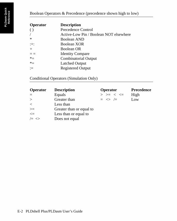
PL
Das
m Q
uic
kR
efer
ence
E-2 PLDshell Plus/PLDasm User’s Guide
Boolean Operators & Precedence (precedence shown high to low)
Operator Description( ) Precedence Control/ Active-Low Pin / Boolean NOT elsewhere* Boolean AND:+: Boolean XOR+ Boolean OR= = Identity Compare*= Combinatorial Output*= Latched Output:= Registered Output
Conditional Operators (Simulation Only)
Operator Description Operator Precedence= Equals > >= < <= High> Greater than = <> /= Low< Less than>= Greater than or equal to<= Less than or equal to/= <> Does not equal
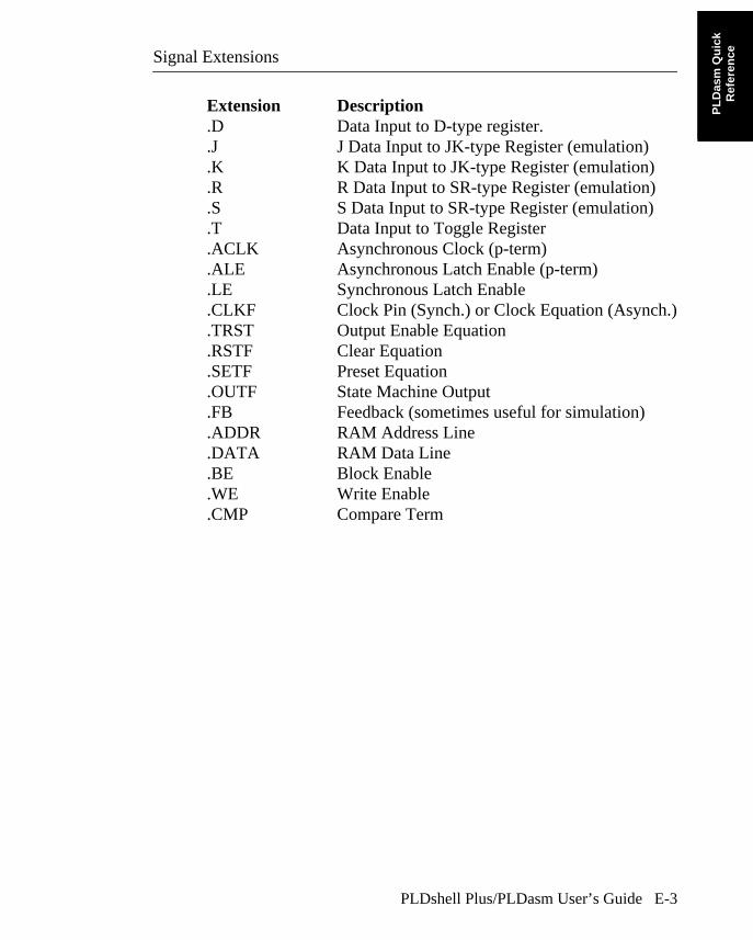
PL
Das
m Q
uic
kR
efer
ence
PLDshell Plus/PLDasm User’s Guide E-3
Signal Extensions
Extension Description.D Data Input to D-type register..J J Data Input to JK-type Register (emulation).K K Data Input to JK-type Register (emulation).R R Data Input to SR-type Register (emulation).S S Data Input to SR-type Register (emulation).T Data Input to Toggle Register.ACLK Asynchronous Clock (p-term).ALE Asynchronous Latch Enable (p-term).LE Synchronous Latch Enable.CLKF Clock Pin (Synch.) or Clock Equation (Asynch.).TRST Output Enable Equation.RSTF Clear Equation.SETF Preset Equation.OUTF State Machine Output.FB Feedback (sometimes useful for simulation).ADDR RAM Address Line.DATA RAM Data Line.BE Block Enable.WE Write Enable.CMP Compare Term

PL
Das
m Q
uic
kR
efer
ence
E-4 PLDshell Plus/PLDasm User’s Guide
PLDshell Example Template
TEMPLATE.PDS, shown below, illustrates the basic sections of a PLDasm file. Reservedwords are shown in bold. This is a reference file only, it is not a working design. AppendixA shows the file SUMMARY.PDS, which illustrates more of the language elements in ameaningful context, and Chapter 4 has a more complete description of the language.
Title PLDasm Example Template (template.pds)Pattern <pattern label>Revision <rev. number>Author <your name>Company <your company>Date <current date>
OPTIONS TURBO = ON ; default is ON SECURITY = OFF ; default is OFF EXPAND = ON ; default is ON INVERSION = ON ; default is ON MINIMIZATION = ON ; default is ON DT_SYNTHESIS = OFF ; default is ON, but not for EP224
; other options are for FLEXlogic devices
CHIP template EP224
; PINLIST
PIN 1 CLKPIN 2 I1 ; Direct InputsPIN 3 I2PIN UPDOWN ; Unassigned pin assignment
PIN Q[0:1] REG ; Unassigned outputs for a state machineNODE Q[2:3] REG ; Unassigned burieds for a state machine
NODE IO27 QSTATUS REG ; Assigned buried, to Macrocell 27
; String substitutions throughout file STRING QADS ' (ADS * PCLK * /RESET) '
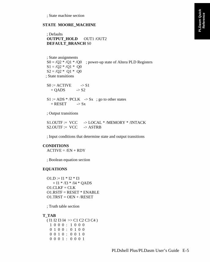
PL
Das
m Q
uic
kR
efer
ence
; State machine section
PLDshell Plus/PLDasm User’s Guide E-5
STATE MOORE_MACHINE
; Defaults OUTPUT_HOLD OUT1 /OUT2 DEFAULT_BRANCH S0
; State assignments S0 = /Q2 * /Q1 * /Q0 ; power-up state of Altera PLD Registers S1 = /Q2 * /Q1 * Q0 S2 = /Q2 * Q1 * Q0 ; State transitions
S0 := ACTIVE -> S1 + QADS -> S2
S1 := ADS * /PCLK -> Sx ; go to other states + RESET -> Sx
; Output transitions
S1.OUTF := VCC -> LOCAL * /MEMORY * /INTACK S2.OUTF := VCC -> ASTRB
; Input conditions that determine state and output transitions
CONDITIONS ACTIVE = /EN + RDY
; Boolean equation section EQUATIONS
O1.D := I1 * I2 * I3 + I1 * /I3 * /I4 * QADS O1.CLKF = CLK O1.RSTF = RESET * ENABLE O1.TRST = OEN + /RESET
; Truth table section
T_TAB ( I1 I2 I3 I4 >> C1 C2 C3 C4 ) 1 0 0 0 : 1 0 0 0 0 1 0 0 : 0 1 0 0 0 0 1 0 : 0 0 1 0 0 0 0 1 : 0 0 0 1
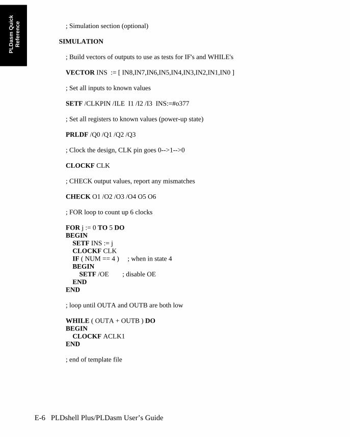
PL
Das
m Q
uic
kR
efer
ence
; Simulation section (optional)
E-6 PLDshell Plus/PLDasm User’s Guide
SIMULATION
; Build vectors of outputs to use as tests for IF's and WHILE's
VECTOR INS := [ IN8,IN7,IN6,IN5,IN4,IN3,IN2,IN1,IN0 ]
; Set all inputs to known values SETF /CLKPIN /ILE I1 /I2 /I3 INS:=#o377
; Set all registers to known values (power-up state) PRLDF /Q0 /Q1 /Q2 /Q3
; Clock the design, CLK pin goes 0-->1-->0
CLOCKF CLK
; CHECK output values, report any mismatches
CHECK O1 /O2 /O3 /O4 O5 O6
; FOR loop to count up 6 clocks
FOR j := 0 TO 5 DO BEGIN SETF INS := j CLOCKF CLK IF ( NUM == 4 ) ; when in state 4 BEGIN SETF /OE ; disable OE END END
; loop until OUTA and OUTB are both low
WHILE ( OUTA + OUTB ) DO BEGIN CLOCKF ACLK1 END
; end of template file

FL
EX
log
ic
Pro
toty
pin
g C
able
PLDshell Plus/PLDasm User’s Guide F-1
Appendix F — FLEXlogic Prototyping Cable
The Altera FLEXlogic device family uses an industry-standard JTAG/IEEE 1149.1interface to support in-circuit reconfiguration and programming. Blank FLEXlogic devicescan be assembled in all locations on the board design and configured or programmed by aboard-level tester.
This Appendix describes how to use the FLEXlogic Prototyping Cable to program andconfigure Altera FLEXlogic devices. There are several possible circuits that can be used orcreated. All can use the JED2JTAG software to control the downloading reconfigurationprocess. See Figure F-1.
Figure F-1 Reconfiguration Circuits
To program the FLEXlogic “shadow” PROM cells, the PENGN software must be usedrather than the JED2JTAG software. PENGN is discussed further in this Appendix.
.HEXFile
JED2JTAGSoftware.SDL
File
JEDECFile(s)
.BINFile
Circuit Type:
Parallel Port Reconfiguration
Custom Reconfiguration Scheme
JTAG.DVC(Part
(i.e., Board Tester or other process)
LIbrary)

FL
EX
log
icP
roto
typ
ing
Cab
le
F-2 PLDshell Plus/PLDasm User’s Guide
JED2JTAG
The JED2JTAG program is a front-end coordinator to several other programs. It handlesall of the protocols and coordinates generation of the intermediate and downloader files. Torun JED2JTAG, use the following command syntax:
jed2jtag <project.sdl>
JED2JTAG uses the following input and output files:
INPUT FILES
project.SDL File describing JTAG chain.
*.JED Device configuration file(s) (JEDEC).
JTAG.DVC Library of JTAG devices.
project.DVC Local project library of JTAG devices. If present in the local directory, it is used instead of JTAG.DVC.
CREATED OUTPUT FILES
project.HEX Hex file for FLASH Memory.
project.BIN JED2JTAG Stream of JTAG signals that is used to create a .HEX file or is sent to a parallel port. Created from .BIT files.
*.BIT JED2JTAG Intermediate file. One .BIT file is created for every .JED file. JED2JTAG checks the time of each .BIT file to each .JED file. If the .JED file is newer, it will recreate the .BIT file.
Creating JTAG Chain Description Files (.SDL)
It is assumed that JEDEC file(s) for devices in the JTAG chain have been generated fromsome design software such as PLDshell Plus. The string description file (.SDL) describesthe JTAG chain on your circuit board.
The file EXAMPLE.SDL contains an example of the chain on a prototype board, as shownin Figure F-2.
FL
EX
log
ic
Pro
toty
pin
g C
able
PLDshell Plus/PLDasm User’s Guide F-3
Figure F-2 EXAMPLE.SDL JTAG Chain
|FILE: example.sdl --Simple Prototype Board{| Port_Num Port_TypeSTRING 3 HEX_FILE
| Loc. Ref Device JEDEC FileDEVICE 0 U3 EPX780QC132RIGHT.JED DEVICE 1 U4 EPX780LC84 LEFT.JED DEVICE 2 U1 PENTIUM }
A ‘|’ indicates a comment line.
Note that DEVICE 2 does not have a JEDEC file associated with it. JED2JTAG will onlyreconfigure FLEXlogic devices with JEDEC files.
STRING Instruction
The STRING instruction in .SDL files controls the operations that JED2JTAG takes for theJTAG chain.
To create an EXAMPLE.HEX file, which can be programmed into a FLASH PROM, usethe following format:
STRING 3 HEX_FILE
To create only an EXAMPLE.BIN file, and no .HEX file, specify the following:
STRING 3 BIN_FILE
JTAGexternal connector
TDI TDO
TMS&TCK
DEV. 0
TDI TDO
TDI TDO
DEV. 1DEV. 2
J1-8 (TDO_PORT)
J1-6 (TDI_PORT)

FL
EX
log
icP
roto
typ
ing
Cab
le
When the chain is similar to that used by the FLEXlogic Prototyping Cable Kit, and can be
F-4 PLDshell Plus/PLDasm User’s Guide
hooked up to a PC parallel port, use the following commands.
To reconfigure a chain on LPT1:
STRING 1 PARALLEL_PORT
To reconfigure a chain on LPT2:
STRING 2 PARALLEL_PORT
NOTE:
See EXAMPLE.SDL for detailed information on configuring port addresses. The configuration varies by machine.
.HEX File Download Information
The following pseudo-code shows the algorithm used to read the contents of the FLASHmemory, and control the JTAG pin signals.
;********************************************************************;* This program typically executes in an embedded controller from an ;* executable memory bank. It transmits data from a local nonvolatile data ;* memory bank to a JTAG (IEEE 1149.1) chain,;* typically to load the SRAM control memory in the FLEXlogic devices in the chain.;* *;* Data is stored in the nonvolatile memory off-line, e.g., with a PROM ;* programmer. It is formatted as a JTAG data stream. Each byte contains;* TDO/TMS data for 4 TCKs. Bit 0 of each byte is the first TDO, bit 1 is the;* first TMS, bit 2 is the second TDO, etc. No inversion occurs between memory ;* nd TMS/TDO.;* *;* The first four bytes in the nonvolatile memory specify the Ending Address + 1.;* The least significant byte is at data address 0. The JTAG data stream starts;* at data address 4.;* *;* The download operation takes place automatically each time the embedded;* controller is reset, including power-on.;********************************************************************; Initialization SET LED# port bit ; turn off LED
DELAY (500) ; delay 500 ms. ; Give time for host JTAG string to completely power-up before beginning.
CLR TCK port bit ; init TCK to LOW CLR RESET# port bit ; init RESET# to LOW (activate host RESET) CLR CE# port bit ; enable Flash memory CLR LED# port bit ; turn on LED
; Transmit data
adrs = 0; ; initialize data address and last_adrs = (adrs) ; last address + 1 (these are 32 bit values) adrs = adrs + 4;

FL
EX
log
ic
Pro
toty
pin
g C
able
WHILE (adrs < last_adrs)
PLDshell Plus/PLDasm User’s Guide F-5
{ ; loop until all data is moved from memory to JTAG chain
; output 1st TMS/TDO MOVE bit 0 of (adrs) to TDO port bit MOVE bit 1 of (adrs) to TMS port bit SET TCK port bit ; pulse TCK CLR TCK port bit
; output 2nd TMS/TDO MOVE bit 2 of (adrs) to TDO port bit MOVE bit 3 of (adrs) to TMS port bit SET TCK port bit ; pulse TCK CLR TCK port bit
; output 3rd TMS/TDO MOVE bit 4 of (adrs) to TDO port bit MOVE bit 5 of (adrs) to TMS port bit SET TCK port bit ; pulse TCK CLR TCK port bit
; output 4th TMS/TDO MOVE bit 6 of (adrs) to TDO port bit MOVE bit 7 of (adrs) to TMS port bit SET TCK port bit ; pulse TCK CLR TCK port bit
adrs = adrs + 1 } ; end while; Completion SET RESET# port bit ; release host SET LED# port bit ; turn off LED SET CE# port bit ; disable memory to save power SLEEP ; disable embedded controller to save power
.BIN File Download Algorithm
The following pseudo-code shows the algorithm used to translate a .BIN file into JTAG pinsignals.
;********************************************************************;* *;* JTAG BINARY FILE DOWNLOAD PSEUDO CODE ;* *;* Author: John Logue ;* Revision Record ;* 11/21/94 JDL Initial Release - Version 1.0 ;* *;********************************************************************;* *;* This program typically executes in a computer, such as a PC, ;* that is capable of reading disk files. It transmits data from ;* a binary file to a JTAG (IEEE 1149.1) chain. Typically, this ;* is to load the SRAM control memory in the FLEXlogic devices in ;* the chain. Normally, the binary file was generated by JED2JTAG. ;* *;* Data in the binary file is formatted as a JTAG data stream. ;* Each byte contains TDO/TMS data for 4 TCKs. Bit 0 of each ;* byte is the first TDO, bit 1 is the first TMS, bit 2 is the ;* second TDO, etc. No inversion occurs between the file data ;* and TMS/TDO. ;* *;* Note that the hardware interface to the JTAG chain is not ;* defined. Examples are: Processor port pins, ISA or ;* Microchannel ports, etc. Refer to Standard IEEE 1149.1 for
FL
EX
log
icP
roto
typ
ing
Cab
le
;* more information on signals TCK, TMS, and TDO.
F-6 PLDshell Plus/PLDasm User’s Guide
;* *;********************************************************************
; Initialization
CLR TCK hw bit ; init TCK to LOW SET RESET hw bit ; activate RESET to FLEXlogic circuitry OPEN bin_file ; open binary file
; Transmit data
DO { ; loop until all data is read from the binary file
READ byte of bin_file into data_byte
IF(END_OF_FILE bin_file) break; exit DO loop if end of file
; output 1st TMS/TDO MOVE bit 0 of data_byte to TDO hw bit MOVE bit 1 of data_byte to TMS hw bit SET TCK hw bit ; pulse TCK CLR TCK hw bit
; output 2nd TMS/TDO MOVE bit 2 of data_byte to TDO hw bit MOVE bit 3 of data_byte to TMS hw bit SET TCK hw bit ; pulse TCK CLR TCK hw bit
; output 3rd TMS/TDO MOVE bit 4 of data_byte to TDO hw bit MOVE bit 5 of data_byte to TMS hw bit SET TCK hw bit ; pulse TCK CLR TCK hw bit
; output 4th TMS/TDO MOVE bit 6 of data_byte to TDO hw bit MOVE bit 7 of data_byte to TMS hw bit SET TCK hw bit ; pulse TCK CLR TCK hw bit
}
; Completion
CLR RESET hw bit ; release RESET to FLEXlogic circuitry CLOSE bin_file ; close binary file MOV TMS,C SETB TCK

FL
EX
log
ic
Pro
toty
pin
g C
able
PLDshell Plus/PLDasm User’s Guide F-7
FLEXlogic JTAG Signals
The FLEXlogic JTAG support consists of an Instruction Register, a Data Register, scancells, and associated logic accessible through the Test Access Port (TAP). The TAPinterface consists of three inputs and one output. The functions of these pins are describedin Table F-1.
The boundary scan cells of any FLEXlogic device is linked to form a shift register chainfor all active pins. This chain provides a path which can be used to shift in test stimulus, aswell as to shift out test response data for inspection.
Standard boundary scan functions such as EXTEST, SAMPLE/PRELOAD, BYPASS, andIDCODE are supported. With these functions you can capture internal logic values, drivedevice pins to a preset value, and identify a device electronically within a chain. In additionto the standard boundary scan instructions, custom functions are also provided that supportdetailed device testing and debug.
The BSDL (Boundary Scan Description Language) files for the FLEXlogic devices areincluded in thePLDshell Plus software.
Table F-1 JTAG Pin Descriptions
Pin Description
TDI The Testability Data Input is the boundary scan serial data input to the FLEX-logic devices.
TDO The Testability Data Output is the boundary scan serial data output from the FLEXlogic devices. JTAG instructions and data are shifted out of the FLEXlogic devices on the TDO output on the falling edge of TCK.
TCK The Testability Clock input provides the boundary scan clock for the FLEXlogic devices. TCK is used to clock state information and data into and out of the de-vices during boundary scan or programming modes.
TMS The Testability Control input is the boundary scan test mode select signal for the FLEXlogic devices.
FL
EX
log
icP
roto
typ
ing
Cab
le
F-8 PLDshell Plus/PLDasm User’s Guide
FLEXlogic Prototyping Cable
Cable Hardware Description
The cable supplied in the Altera FLEXlogic Prototyping Cable Kit consists of a maleDB-25 connector containing a circuit board, and a flat ribbon cable ending in a female 20-pin connector. The circuit board housed in the DB-25 connector shell contains an integratedline driver. The cable supports the four TAP interface signals (TDI, TDO, TCK, and TMS)plus some additional signal signals useful for debug (STEP, RUN, and RESET).
Installation
The FLEXlogic Prototyping Cable connects between a PC parallel port and a male 20-pinconnector mounted on the target application circuit board. For a single FLEXlogic device,the PC cable TAP interface signals connect directly to the appropriate pins on the device.For multiple FLEXlogic devices, the JTAG TDI and TDO signals are connected in a “daisychain.” In this case, the TDO_PORT from the cable connects to the “last” logical device(first physical device) in the chain. In turn, this device’s TDO pin connects the next logicdevice’s TDI pin, and so forth. The chain is completed by connecting the TDO pin of the“first” logical device (DEV 0) to the TDI_PORT on the cable connector (see Figure E-3).The TMS and TCK cable signals connect directly to the corresponding RMS and TCK pinson each device in the JTAG chain
FLEXlogic Prototyping Cable Signals
The functions of the FLEXlogic Prototyping Cable signals are described in Table F-2.
Table F-2 FLEXlogic Prototyping Cable Signals
Vcc 1 +5V +/- 250mV must be supplied by the target application circuit. This supplies power to the cable line driver located in the shell of the DB-25 connector.
TMS 2 JTAG Testability Control Signal, provided by the JTAG software; connect to the TMS pin of each device in the JTAG chain.
GND 3,5,7,11,13,15,17
Connect ALL GND lines to ground to reduce noise.
TCK 4 JTAG Testability Clock signal, provided by JTAG software; connect to the TCK pin of each device in the JTAG chain.
TDI_PORT 6 JTAG Testability Data output; connect to TDO pin of “first” device in JTAG chain.

FL
EX
log
ic
Pro
toty
pin
g C
able
Table F-2 FLEXlogic Prototyping Cable Signals (Continued)
PLDshell Plus/PLDasm User’s Guide F-9
*Note: Vpp must be decoupled with a 0.1-uF ceramic capacitor at the Vpp pin of the device.In addition, decouple the Vpp power source at the board entry point with both a 0.1-uFcapacitor and a larger tantalum electrolytic capacitor (1uF to 10uF).
Schematic
Figure F-3 shows the FLEXlogic Prototype Cable interface and JTAG “daisy chain,” andthe schematic diagram of the FLEXlogic Prototyping Cable Interface.
TDO_PORT 8 JTAG Testability Data Input; connect to TDI pin of “last” logical device in JTAG chain.
VPP_SENSE 9 (Optional) Reserved for future use.
VPP_ON 10 (Optional) Active high signal, provided by JTAG software, to activate on-board Vpp power source.
STEP# 12 (Optional) Active low debug signal reserved for future use.
RUN# 14 (Optional) Active low debug signal reserved for future use.
RESET# 16 (Optional) Active low signal provided by the JED2JTAG software. This signal is driven low during device reconfiguration. The PENGN program does not activate this signal.
VPP_OK# 18 An active low signal checked by JTAG software prior to device programming. Tie this signal low if an external Vpp source is used.
VPP* 19,20 A +12.75V +/- 250mV programming voltage supplied by an external supply. The FLEXlogic Prototyping Cable, which is attached to the PC, does not supply the programming voltage. Permanent device damage may occur if Vpp exceeds 13.5V.

FL
EX
log
icP
roto
typ
ing
Cab
le
F-10 PLDshell Plus/PLDasm User’s Guide
Figure F-3 FLEXlogic Prototyping Cable Interface
DB-25 Printer Port
Flat Ribbon Cable
121416
11,13,15,1718
19,20
STEP#RUN#RESET#GNDVPP_OK#VPP*
VCCTMSGNDTCKTDI_PORTTDO_PORTVPP_SENSEVPP_ON
TDI_PORT Signal (pin 6)
TDO_PORT Signal (pin 8)
20-PinConnector
Target Application Board
12
3,5,74689
10
(line 1 in blue)
Connector & Logic
NOTE: 1) VPP_SENSE, STEP#, and RUN# are reserved for future use.
TDI
IC1DEV 3
TDO
TDO
EPX780DEV 0
TDI TDO
EPX740DEV 1
TDI
TDI
IC1DEV 2
TDO
2
43
65
87
109
1211
1413
1615
1817
2019
1
(component side)
FL
EX
log
ic P
roto
typ
ing
Cab
le

FL
EX
log
ic
Pro
toty
pin
g C
able
PLDshell Plus/PLDasm User’s Guide F-11
PENGN Software Description
The PENGN program is used to program the FLEXlogic devices using the FLEXlogicPrototyping Cable. This program can be run from the PLDshell Run Menu or the Utilities—Invoke Command Shell submenu. Figure F-4 illustrates the PENGN program flow.
Figure F-4 PENGN Program Flow
Commands
PENGN has the following command syntax:
PENGN [options] file[.jed]
where the options are:
-part P Target device is part P.Only the FLEXlogic device family is supported. Valid part names are shown in Table 1-1 in this manual.
PENGN - APLProgramming
SoftwareJEDEC
File
JPMFile
APLFile
BITMAPFile
JTAG String
EPXxxxx
FLEXlogic Device
DATABASEJEDEC to PHYSICAL
PROGRAMMINGALGORITHM
PROGRAMMING or RECONFIGURATIONVECTOR File

FL
EX
log
icP
roto
typ
ing
Cab
le
F-12 PLDshell Plus/PLDasm User’s Guide
-port N Hardware is connected to LPT1 or LPT2.This option must be specified and only the values of 1 and 2 are val-id. These correspond to ports LPT1 and LPT2 respectively.
-loc N Target device is located at position 0, 1, 2 ... N.This option must be specified and refers to the physical location in the JTAG string where the target device exists. The value starts counting from 0. If a target device has its TDO line connected to the cable connection and not another device in the string, its location is 0. When using the starter kit, the location is always 0 or 1.
-pe-ps-re-rs
Program the devices’ EPROMProgram the devices’ SRAMRead the devices’ EPROMRead the devices’ SRAMOnly one of these options must be specified. These determine what the action is to be. One of these is not necessary if option ‘-be’ or ‘-bs’ is specified.
-v Verify the programming of SRAM or EPROM.This option may be omitted. When present and a program option has been selected, the software will perform verification of the download.
-sp S Set the devices’ Security Bits where S is ON or OFF.This option may be omitted. When specified, the devices’ security bit(s) will be set to whether ON or OFF.
-be file[.bit]-bs file[.bit]
This option overrides any condition preset in the JEDEC file.Create a EPROM programming bit map file.Create an SRAM programming bit map file.These options may be omitted. When specified, they cause the software to generate a JTAG stream bitmap file. This file may be used by external software to program the device via other means.
-jd file[.dvc] JTAG device file is [file.dvc].This option may be omitted. When present, this file overrides the standard default device file. The standard file is JTAG.DVC. This file is described at the end of this section.
-js file[.sdl] JTAG string file is [file.sdl].This option may be omitted. When present, this file overrides the standard default string file. Describes the user’s JTAG string. This file is described at the end of this section.
-f Process has been forked
-e elog Produce an error trace log in file ELOG.

FL
EX
log
ic
Pro
toty
pin
g C
able
PLDshell Plus/PLDasm User’s Guide F-13
Usage Examples
The following examples show how to use PENGN commands.
Example 1
Program the EPROM of an EPX780 device in a 132-pin package with the JEDEC fileBUSCNTRL.JED, at JTAG string location 1, which is connected to parallel port LPT1.
Enter the command:
pengn -part epx780QC132 -loc 1 -port 1 -pe buscntrl
This command starts PENGN and displays the following:
PENGN Release [ Vx.y ] SID [ Vx.y ](C) Copyright 1990, 1991, 1992 Altera Corporation
INFO PENGN: Interpreting file: epx780.apl.
Reading JEDEC buscntrl.jed 0: ..........10240: ..........20480: ..........30720: .31704: Done
Target Device ID = [0062103h]Writing to EPX780's EPROM
1 : ..........11: ..........21: ..........31: ..........41: ..........51: ....54: Done
-d Debug mode, sets debug := 1. Otherwise disabled.
-s path Additional search paths (up to 16 are allowed).
-l lib Additional libraries to load (up to 16 are allowed).
-i Interactive mode. Return to user after startup.
-a file Alternate APL file.

FL
EX
log
icP
roto
typ
ing
Cab
le
Example 2
F-14 PLDshell Plus/PLDasm User’s Guide
Program the SRAM of an EPX780 device in a 132-pin package with the JEDEC fileBUSCNTRL.JED, at JTAG string location 1 which is connected to parallel port LPT1.
Enter the command:
pengn -part epx780qc132 -loc 1 -port 1 -ps buscntrl
This command starts PENGN and displays the following:
PENGN Release [ Vx.y ] SID [ Vx.y ](C) Copyright 1990, 1991, 1992 Altera Corporation
INFO PENGN: Interpreting file: epx780.apl.
Reading JEDEC buscntrl.jed 0: ..........10240: ..........20480: ..........30720: .31704: Done
Target Device ID = [0062103h]Writing to EPX780's SRAM
1 : ..........11: ..........21: ..........31: ..........41: ..........51: ....54: Done
Example 3
Program the SRAM of an EPX780 device in an 84-pin package with the JEDEC fileBUSCNTRL.JED, at JTAG string location 1 which is connected to parallel port LPT1.Additionally, the command line performs a verify of the downloaded data and generates anEPROM bitmap file, BUSCNTRL.BIT.
Enter the command:
pengn -part epx780lc84 -loc 1 -port 1 -ps -v -be buscntrl buscntrl
This command starts PENGN and displays the following:
FL
EX
log
ic
Pro
toty
pin
g C
able
PENGN Release [ Vx.y ] SID [ Vx.y ]
PLDshell Plus/PLDasm User’s Guide F-15
(C) Copyright 1990, 1991, 1992 Altera Corporation
INFO PENGN: Interpreting file: epx780.apl.
Reading JEDEC buscntrl.jed 0: ..........10240: ..........20480: ..........30720: .31704: Done
Target Device ID = [1062103h]Writing to EPX780's SRAM
1 : ..........11: ..........21: ..........31: ..........41: ..........51: ....54: Done
Verify to EPX780's SRAM1 : ..........11: ..........21: ..........31: ..........41: ..........51: ....54: Done
Generating a EPX780 EPROM Bitmap file1 : ..........11: ..........21: ..........31: ..........41: ..........51: ....54: Done
Example 4
Generate an EPROM bitmap file (BUSCNTRL.BIT) of an EPX780 device in an 84-pinpackage with the JEDEC file BUSCNTRL.JED.
Enter the command:
pengn -part epx780lc84 -be buscntrl buscntrl
This command starts PENGN and displays the following:

FL
EX
log
icP
roto
typ
ing
Cab
le
PENGN Release [ Vx.y ] SID [ Vx.y ]
F-16 PLDshell Plus/PLDasm User’s Guide
(C) Copyright 1990, 1991, 1992 Altera Corporation
INFO PENGN: Interpreting file: epx780.apl.
Reading JEDEC buscntrl.jed 0: ..........10240: ..........20480: ..........30720: .31704: Done
Generating a EPX780 EPROM Bitmap file1 : ..........11: ..........21: ..........31: ..........41: ..........51: ....54: Done
PENGN Errors
Refer to Appendix D for documentation on PENGN errors. If any error you encounter isnot covered there, try the on-line documentation within the PLDshell PLUS software.
If any error occurs related to the hardware or JTAG string, try running theTAPLOGIC.EXE program to help diagnose the problem. This program is located in thePLDshell Plus installation directory.
Sample Design - Parallel Port Reconfiguration
This section provides an overview of a typical reconfiguration operation.
The reconfiguration operation includes the following steps:
1. Enter the design using either PLDshell Plus or a third-party tool and generate a JEDEC file.
2. Make sure the downloader cable is connected properly to both the PC parallel port and the target application.
3. Check that the Vcc power supply for the target application is on.
4. Use the JED2JTAG software to download the JEDEC file.
5. Repeast the process as many times as desired.
FL
EX
log
ic
Pro
toty
pin
g C
able
PLDshell Plus/PLDasm User’s Guide F-17
Programming Example
The differences between a reconfiguration download operation and a programmingoperation are as follows:
• The PENGN program is used to program a device, whereas JED2JTAG is used only fordevice configuration.
• A Vpp supply (12.75V) must be provided to the target application and should only beswitched on after the Vcc supply is stable. The Vpp supply should also be removedbefore the Vcc supply is powered down. The Altera downloader cable includes a Vppcontrol signal that automatically enables and disables Vpp for the target application.
• For the EPX780 and EPX740 FLEXlogic devices, programming may only be performedone time.
JTAG Device Library
The JTAG.DVC Device Type Definitions file included in the PLDshell Plus installationdirectory contains a description of several common JTAG devices, including theFLEXlogic devices. Additional device types can be defined easily in the JTAG.DVC file,which includes directions that show the type of information needed. Typically, only thelength of the instruction register is required.
Information on each device type in the file is placed in a block, which is delineated by openand closed brackets. Comments are noted with a vertical bar (|). All information in a linefollowing a vertical bar is treated as a comment. Each line in a block can have two or threearguments, separated by spaces or tab characters. The first argument is always a keywordin ASCII. The remaining arguments are decimal numbers, hexadecimal numbers, or ASCIIstrings. Keywords must be in upper case.
The following paragraphs describe each keyword:
ID — The second argument in this line is a 32-bit unsigned hexadecimal number thatmatches the Device Identification code. This is the data value that will be read from the chipwhen JTAG command IDCODE is in effect. If the chip does not provide an IDCODE, thesecond argument in this line should be 0 (an illegal Device Identification code). Thereshould be only one ID line in each block.
NAME — The second argument in this line is a descriptive name for the device in ASCII.This can be up to 31 characters in length. This name is used by String Device List file toidentify devices that don’t have an ID code (see String Device List file description, below).There should be only one NAME line in each block.

FL
EX
log
icP
roto
typ
ing
Cab
le
IR_LENGTH
— The second argument in this line is a decimal number that specifies the
F-18 PLDshell Plus/PLDasm User’s Guide
number of bits in the instruction register in this device. There should be only oneIR_LENGTH line in each block.
DR_LENGTH — The third argument in this line is a decimal number that specifies thenumber of bits in the data register in this device when the instruction specified in the secondargument is in effect. The instruction specified in the second argument is in hexadecimalnotation. There should be one DR_LENGTH line in each block for each instruction in thedevice.
Figure F-5 shows a sample .DVC file.
Figure F-5 Sample Device Type Definitions File
String Device List File
The String Device List file (extension .SDL) provides information about each JTAG stringin the system. One or more JTAG strings can be defined in this file. This file is optional.However, if a JTAG string is defined in this file, the restriction that Altera devices must beplaced at the end of the JTAG string no longer applies. It also assigns a reference designator(e.g., U23) to each device in the string. This reference designator makes it easy for the userto later reference each device during programming, debug, etc.
| Altera EPX780, 84 pin PLCC{ID 10621013NAME EPX780LC84IR_LENGTH 5| Instruction hex Data Length <decimal>DR_LENGTH 00 264 | EXTESTDR_LENGTH 1F 1 | BYPASSDR_LENGTH 01 264 | SAMPLE/PRELOADDR_LENGTH 02 32 | IDCODEDR_LENGTH 16 600 | UESCODEDR_LENGTH 04 1 | HIZ}| Altera EPX780, 132 pin PQFP{ID 00621013NAME EPX780QC132IR_LENGTH 5| Instruction hex Data Length <decimal>DR_LENGTH 00 264 | EXTESTDR_LENGTH 1F 1 | BYPASSDR_LENGTH 01 264 | SAMPLE/PRELOADDR_LENGTH 02 32 | IDCODEDR_LENGTH 16 600 | UESCODEDR_LENGTH 04 1 | HIZ}

FL
EX
log
ic
Pro
toty
pin
g C
able
Information on each string is placed in a block, which is delimited by open and closed
PLDshell Plus/PLDasm User’s Guide F-19
brackets. Comments are noted with a vertical bar (|). All information in a line following avertical bar is treated as a comment.
Each line in a block can have two or four arguments, separated by spaces or tab characters.The first argument is always a keyword in ASCII. The remaining arguments are decimalnumbers or ASCII strings. Keywords must be in uppercase characters.
The following paragraphs describe each keyword:
STRING — The second argument in this line is a decimal number specifying the stringthat is defined by this block (either 1 or 2 in the initial system). There should be only oneSTRING line in each block.
DEVICE — Each DEVICE line relates a device position in the string to a device type,which was previously defined in the Device Type Definitions file. The DEVICE line alsorelates a device position in the string to a reference designator, which can be used to relatethese devices to schematic diagrams, net lists, etc. There should be one DEVICE line ineach block for each device in the JTAG string. DEVICE lines may be in any order withinthe block.
The second argument in the line is a decimal number specifying the device location in theJTAG string. Devices in the string are numbered 0 through n. Device 0 is the IC whoseTDO pin is connected to the JTAG port.
The third argument in the line is the Reference Designator in ASCII. It can be up to 7characters long.
The fourth and last argument in the line is the Device Name. It is an ASCII string of up to31 characters. If the device does not have an ID Code, this argument will be used to definethe device type. It must be identical to the corresponding NAME line argument in theDevice Type Definitions file. This comparison is case sensitive.
Figure F-6 shows a sample .SDL file.
Figure F-6 Sample String Device List File
| STRING/NAME DEFINITIONS
{| String_numberSTRING 1| Loc Ref_des Device_type_nameDEVICE 0 U2 EPX780LC84DEVICE 1 U3 TI_74BCT8373DEVICE 2 U4 TI_74BCT8373DEVICE 3 U1 TI_74BCT8374}