Embed Size (px)
Citation preview
1
DIGITAL TECHNICS
Dr. Bálint Pődör
Óbuda University,
Microelectronics and Technology Institute
5b. LECTURE: SEQUENTIAL CIRCUITS BASICS
AND FLIP-FLOPS
1st (Autumn) term 2018/2019
5. LECTURE
1. Sequential logic, basic principles
2. Synchronous and asynchronous logic circuits
3. Flip-flops
2
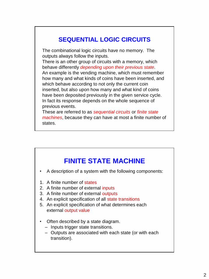
SEQUENTIAL LOGIC CIRCUITS
The combinational logic circuits have no memory. The
outputs always follow the inputs.
There is an other group of circuits with a memory, which
behave differently depending upon their previous state.
An example is the vending machine, which must remember
how many and what kinds of coins have been inserted, and
which behave according to not only the current coin
inserted, but also upon how many and what kind of coins
have been deposited previously in the given service cycle.
In fact its response depends on the whole sequence of
previous events.
These are referred to as sequential circuits or finite state
machines, because they can have at most a finite number of
states.
FINITE STATE MACHINE
• A description of a system with the following components:
1. A finite number of states
2. A finite number of external inputs
3. A finite number of external outputs
4. An explicit specification of all state transitions
5. An explicit specification of what determines each
external output value
• Often described by a state diagram.
– Inputs trigger state transitions.
– Outputs are associated with each state (or with each
transition).
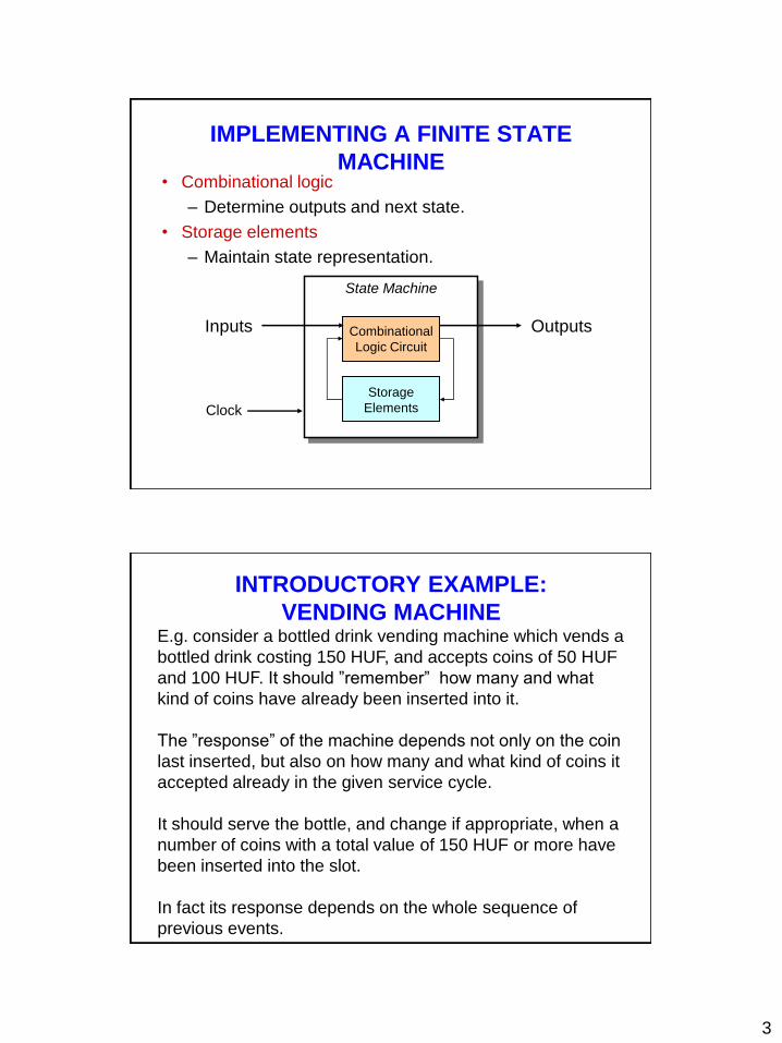
3
IMPLEMENTING A FINITE STATE
MACHINE • Combinational logic
– Determine outputs and next state.
• Storage elements
– Maintain state representation.
State Machine
Combinational
Logic Circuit
Storage
Elements
Inputs Outputs
Clock
INTRODUCTORY EXAMPLE:
VENDING MACHINE E.g. consider a bottled drink vending machine which vends a
bottled drink costing 150 HUF, and accepts coins of 50 HUF
and 100 HUF. It should ”remember” how many and what
kind of coins have already been inserted into it.
The ”response” of the machine depends not only on the coin
last inserted, but also on how many and what kind of coins it
accepted already in the given service cycle.
It should serve the bottle, and change if appropriate, when a
number of coins with a total value of 150 HUF or more have
been inserted into the slot.
In fact its response depends on the whole sequence of
previous events.
4
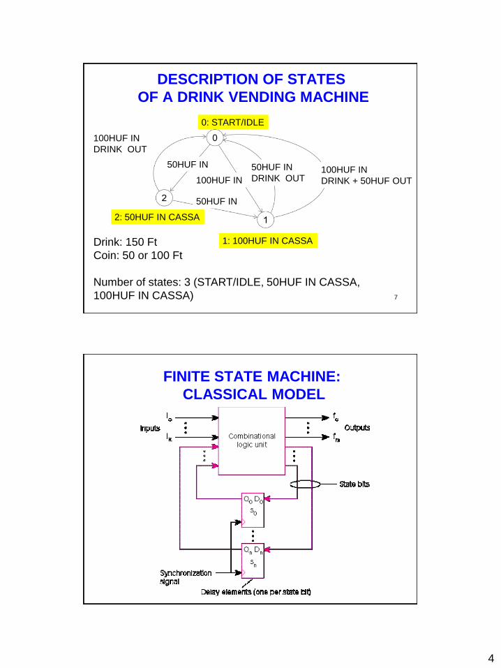
7
DESCRIPTION OF STATES
OF A DRINK VENDING MACHINE
Drink: 150 Ft
Coin: 50 or 100 Ft
Number of states: 3 (START/IDLE, 50HUF IN CASSA,
100HUF IN CASSA)
0: START/IDLE
2: 50HUF IN CASSA
1: 100HUF IN CASSA
100HUF IN
DRINK + 50HUF OUT
100HUF IN
DRINK OUT
50HUF IN
DRINK OUT
50HUF IN
50HUF IN
100HUF IN
FINITE STATE MACHINE:
CLASSICAL MODEL
5
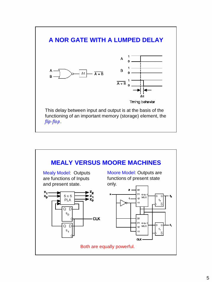
A NOR GATE WITH A LUMPED DELAY
This delay between input and output is at the basis of the
functioning of an important memory (storage) element, the
flip-flop.
MEALY VERSUS MOORE MACHINES
Mealy Model: Outputs
are functions of Inputs
and present state.
Moore Model: Outputs are
functions of present state
only.
Both are equally powerful.
6
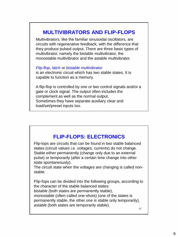
MULTIVIBRATORS AND FLIP-FLOPS
Multivibrators, like the familiar sinusoidal oscillators, are
circuits with regenerative feedback, with the difference that
they produce pulsed output. There are three basic types of
multivibrator, namely the bistable multivibrator, the
monostable multivibrator and the astable multivibrator.
Flip-flop, latch or bistable multivibrator
is an electronic circuit which has two stable states. It is
capable to function as a memory.
A flip-flop is controlled by one or two control signals and/or a
gate or clock signal. The output often includes the
complement as well as the normal output.
Sometimes they have separate auxiliary clear and
load/set/preset inputs too.
12
FLIP-FLOPS: ELECTRONICS
Flip-lops are circuits that can be found in two stable balanced
states (circuit values i.e. voltages, currents) do not change.
Stable either permanently (change only due to an external
pulse) or temporarily (after a certain time change into other
state spontaneously).
The circuit state when the voltages are changing is called non-
stable.
Flip-fops can be divided into the following groups, according to
the character of the stable balanced states:
bistable (both states are permanently stable),
monostable (often called one-shots) (one of the states is
permanently stable, the other one is stable only temporarily),
astable (both states are temporarily stable).
7
13
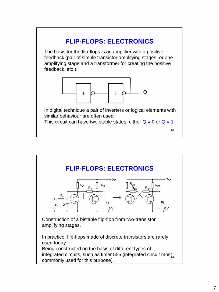
FLIP-FLOPS: ELECTRONICS
The basis for the flip-flops is an amplifier with a positive
feedback (pair of simple transistor amplifying stages, or one
amplifying stage and a transformer for creating the positive
feedback, etc.).
In digital technique a pair of inverters or logical elements with
similar behaviour are often used.
This circuit can have two stable states, either Q = 0 or Q = 1
1 1 Q
14
FLIP-FLOPS: ELECTRONICS
Construction of a bistable flip-flop from two-transistor
amplifying stages.
In practice, flip-flops made of discrete transistors are rarely
used today.
Being constructed on the basis of different types of
integrated circuits, such as timer 555 (integrated circuit most
commonly used for this purpose).
8
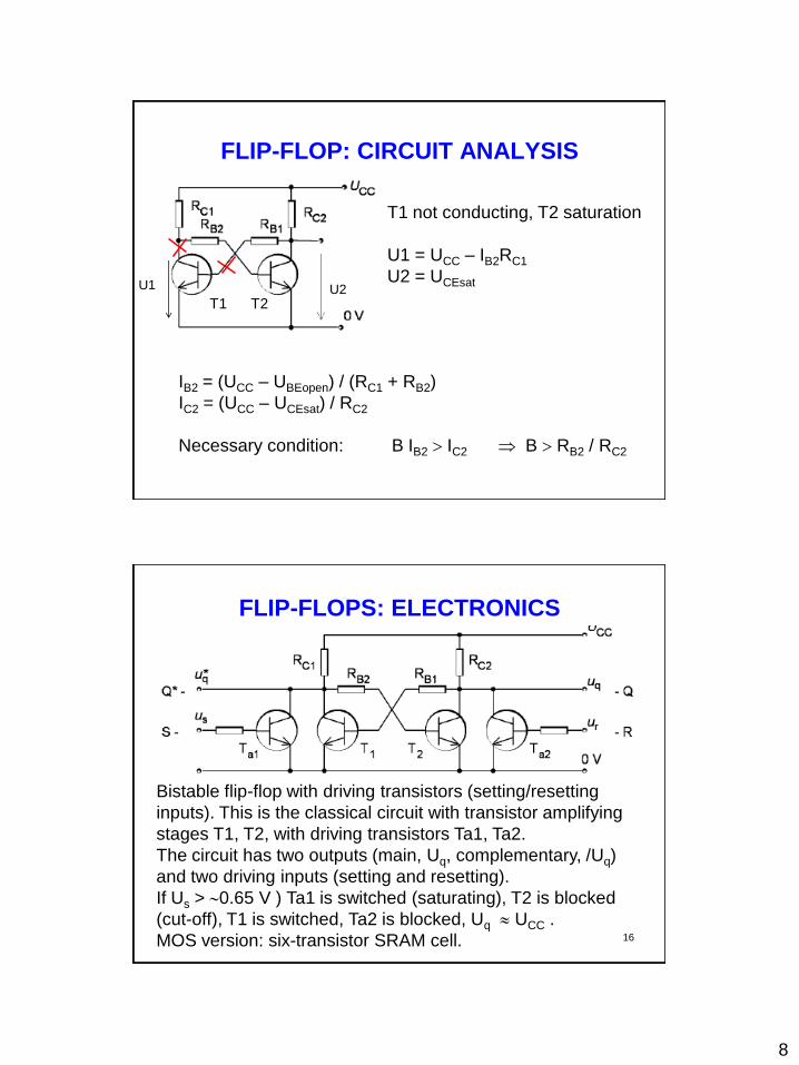
FLIP-FLOP: CIRCUIT ANALYSIS
T1 T2
U1 U2
T1 not conducting, T2 saturation
U1 = UCC – IB2RC1
U2 = UCEsat
IB2 = (UCC – UBEopen) / (RC1 + RB2)
IC2 = (UCC – UCEsat) / RC2
Necessary condition: B IB2 IC2 B RB2 / RC2
16
FLIP-FLOPS: ELECTRONICS
Bistable flip-flop with driving transistors (setting/resetting
inputs). This is the classical circuit with transistor amplifying
stages T1, T2, with driving transistors Ta1, Ta2.
The circuit has two outputs (main, Uq, complementary, /Uq)
and two driving inputs (setting and resetting).
If Us > 0.65 V ) Ta1 is switched (saturating), T2 is blocked
(cut-off), T1 is switched, Ta2 is blocked, Uq UCC .
MOS version: six-transistor SRAM cell.
9
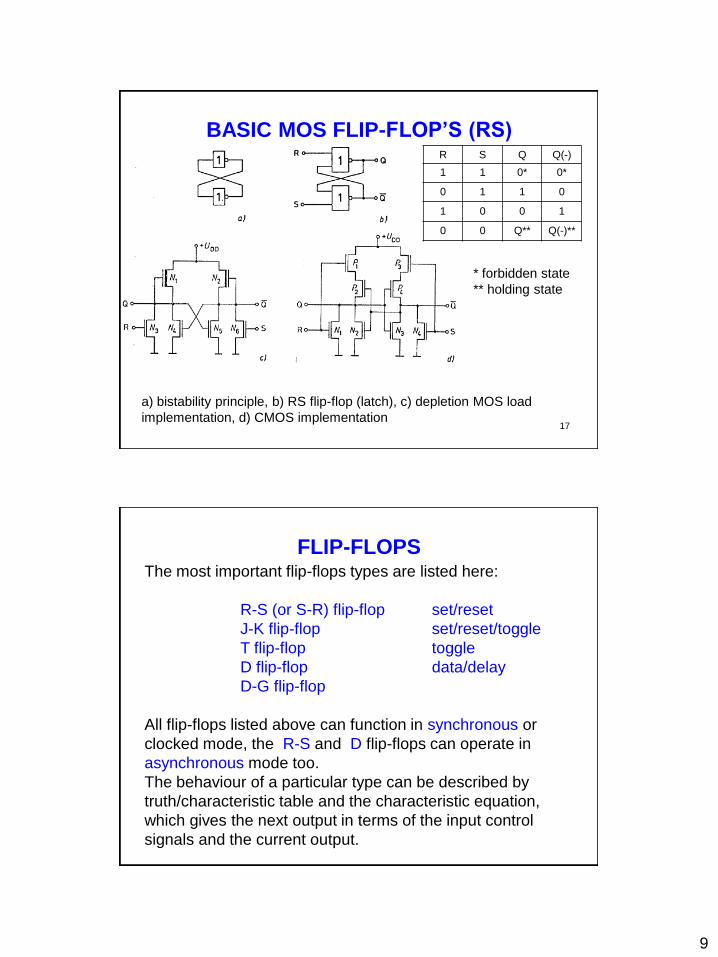
BASIC MOS FLIP-FLOP’S (RS)
17
R S Q Q(-)
1 1 0* 0*
0 1 1 0
1 0 0 1
0 0 Q** Q(-)**
a) bistability principle, b) RS flip-flop (latch), c) depletion MOS load
implementation, d) CMOS implementation
* forbidden state
** holding state
FLIP-FLOPS The most important flip-flops types are listed here:
R-S (or S-R) flip-flop set/reset
J-K flip-flop set/reset/toggle
T flip-flop toggle
D flip-flop data/delay
D-G flip-flop
All flip-flops listed above can function in synchronous or
clocked mode, the R-S and D flip-flops can operate in
asynchronous mode too.
The behaviour of a particular type can be described by
truth/characteristic table and the characteristic equation,
which gives the next output in terms of the input control
signals and the current output.
10
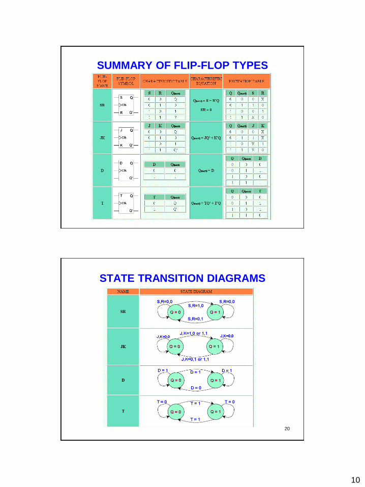
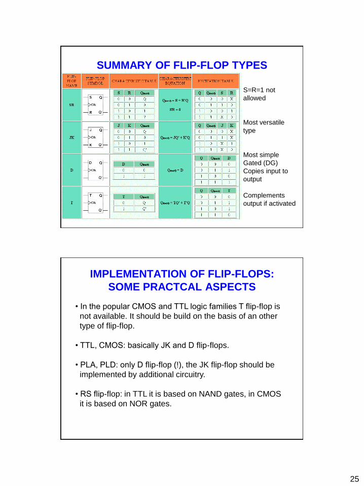
SUMMARY OF FLIP-FLOP TYPES
STATE TRANSITION DIAGRAMS
20
11
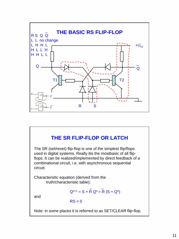
THE BASIC RS FLIP-FLOP
+Ucc
R S
Q _
Q
T1 T2
• •
• •
_
R S Q Q
L L no change
L H H L
H L L H
H H L L
THE SR FLIP-FLOP OR LATCH
The SR (set/reset) flip-flop is one of the simplest flip/flops
used in digital systems. Really itis the mostbasic of all flip-
flops. It can be realized/implemented by direct feedback of a
combinational circuit, i.e. with asynchronous sequential
circuit.
Characteristic equation (derived from the
truth/characteristic table):
_ _
Qn+1 = S + R Qn = R (S + Qn)
and
RS = 0
Note: in some places it is referred to as SET/CLEAR flip-flop.
12
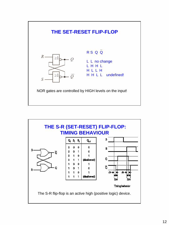
THE SET-RESET FLIP-FLOP
_
R S Q Q
L L no change
L H H L
H L L H
H H L L undefined!
NOR gates are controlled by HIGH levels on the input!
THE S-R (SET-RESET) FLIP-FLOP:
TIMING BEHAVIOUR
The S-R flip-flop is an active high (positive logic) device.
13
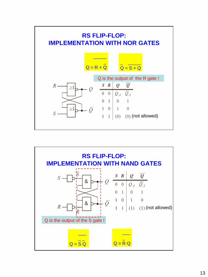
RS FLIP-FLOP:
IMPLEMENTATION WITH NOR GATES
Q is the output of the R gate !
_____
_
Q = R + Q
(not allowed)
_ _____
Q = S + Q
RS FLIP-FLOP:
IMPLEMENTATION WITH NAND GATES
Q is the output of the S gate !
(not allowed)
___
_ _
Q = S Q
___
_
Q = R Q
14
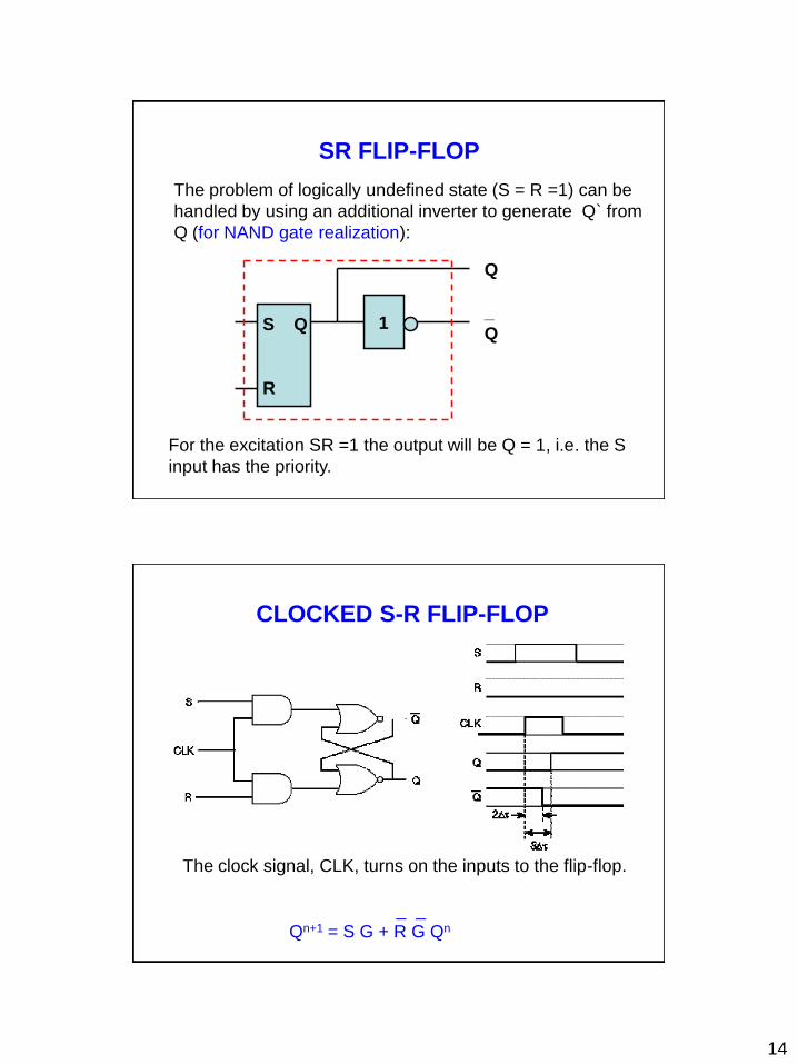
SR FLIP-FLOP
The problem of logically undefined state (S = R =1) can be
handled by using an additional inverter to generate Q` from
Q (for NAND gate realization):
S Q
R
1
Q
_
Q
For the excitation SR =1 the output will be Q = 1, i.e. the S
input has the priority.
CLOCKED S-R FLIP-FLOP
The clock signal, CLK, turns on the inputs to the flip-flop.
_ _
Qn+1 = S G + R G Qn
15
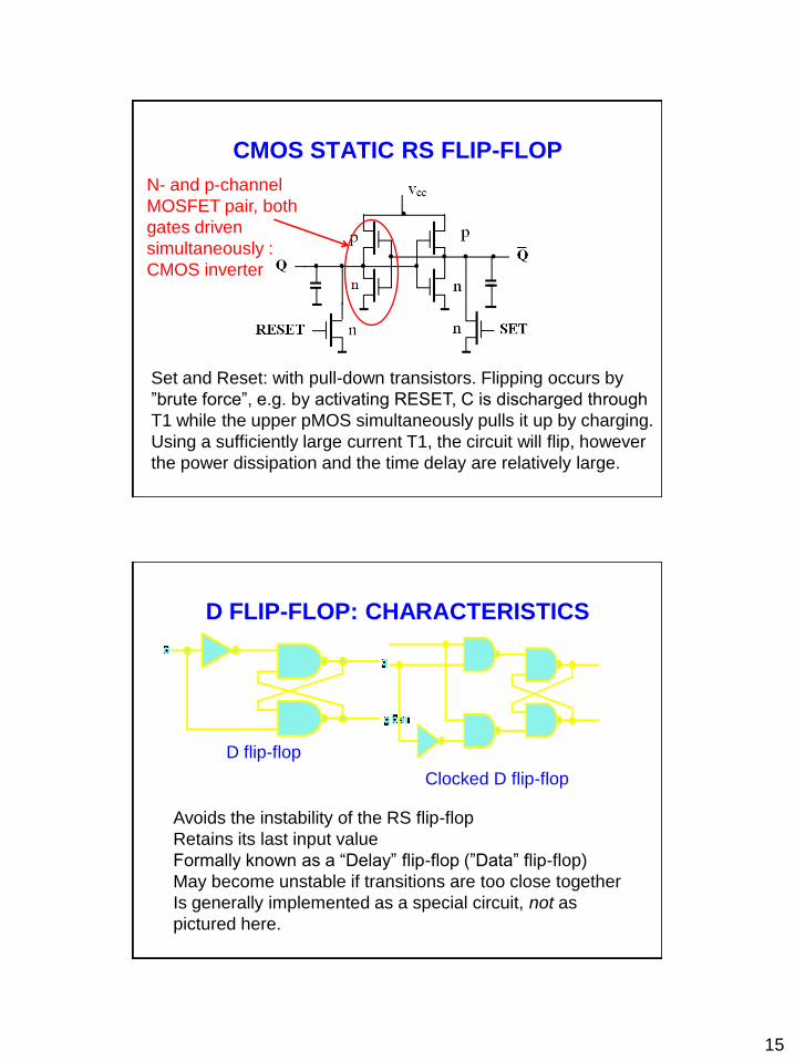
CMOS STATIC RS FLIP-FLOP
Set and Reset: with pull-down transistors. Flipping occurs by
”brute force”, e.g. by activating RESET, C is discharged through
T1 while the upper pMOS simultaneously pulls it up by charging.
Using a sufficiently large current T1, the circuit will flip, however
the power dissipation and the time delay are relatively large.
N- and p-channel
MOSFET pair, both
gates driven
simultaneously :
CMOS inverter
D FLIP-FLOP: CHARACTERISTICS
D flip-flop
Clocked D flip-flop
Avoids the instability of the RS flip-flop
Retains its last input value
Formally known as a “Delay” flip-flop (”Data” flip-flop)
May become unstable if transitions are too close together
Is generally implemented as a special circuit, not as
pictured here.
16
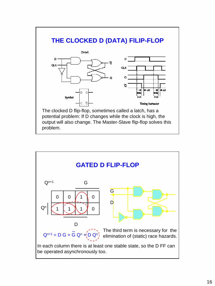
THE CLOCKED D (DATA) FlLIP-FLOP
The clocked D flip-flop, sometimes called a latch, has a
potential problem: If D changes while the clock is high, the
output will also change. The Master-Slave flip-flop solves this
problem.
GATED D FLIP-FLOP
0
1
0 1 0
1 1 0
G
D
Qn
Qn+1
_
Qn+1 = D G + G Qn + D Qn
G
D
The third term is necessary for the
elimination of (static) race hazards.
In each column there is at least one stable state, so the D FF can
be operated asynchronously too.
17
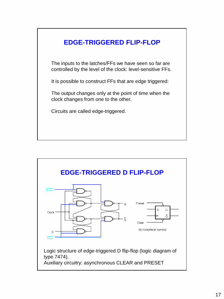
EDGE-TRIGGERED FLIP-FLOP
The inputs to the latches/FFs we have seen so far are
controlled by the level of the clock: level-sensitive FFs.
It is possible to construct FFs that are edge triggered:
The output changes only at the point of time when the
clock changes from one to the other.
Circuits are called edge-triggered.
EDGE-TRIGGERED D FLIP-FLOP
Logic structure of edge-triggered D flip-flop (logic diagram of
type 7474).
Auxiliary circuitry: asynchronous CLEAR and PRESET
18
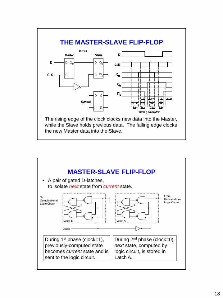
THE MASTER-SLAVE FLIP-FLOP
The rising edge of the clock clocks new data into the Master,
while the Slave holds previous data. The falling edge clocks
the new Master data into the Slave.
MASTER-SLAVE FLIP-FLOP
• A pair of gated D-latches,
to isolate next state from current state.
During 1st phase (clock=1),
previously-computed state
becomes current state and is
sent to the logic circuit.
During 2nd phase (clock=0),
next state, computed by
logic circuit, is stored in
Latch A.
19
MASTER-SLAVE D FLIP-FLOP:
LOGIC DIAGRAM
Auxiliary circuitry: asynchronous CLEAR and PRESET
FLIP-FLOP TIMING PARAMETERS
Certain timing parameters would be listed in the specification
sheet of a flip-flop. Some of these parameters, are specific to
the logic family to which the flip-flop belongs. There are some
parameters that have different values for different flip-flops
belonging to the same broad logic family. It is therefore
important that one considers these timing parameters
before using a certain flip-flop in a given application. Some of
the important ones are set-up and hold times, propagation
delay, clock pulse HIGH and LOW times, asynchronous input
active pulse width, clock transition time and maximum clock
frequency.
20
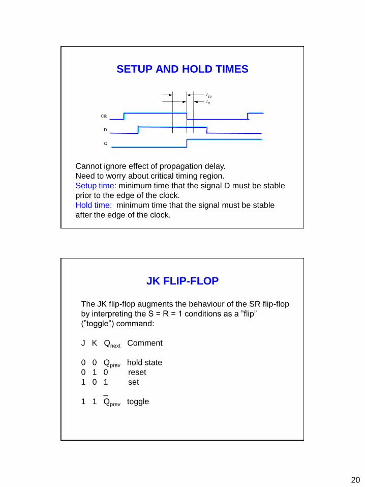
SETUP AND HOLD TIMES
Cannot ignore effect of propagation delay.
Need to worry about critical timing region.
Setup time: minimum time that the signal D must be stable
prior to the edge of the clock.
Hold time: minimum time that the signal must be stable
after the edge of the clock.
JK FLIP-FLOP
The JK flip-flop augments the behaviour of the SR flip-flop
by interpreting the S = R = 1 conditions as a ”flip”
(”toggle”) command:
J K Qnext Comment
0 0 Qprev hold state
0 1 0 reset
1 0 1 set
_
1 1 Qprev toggle
21
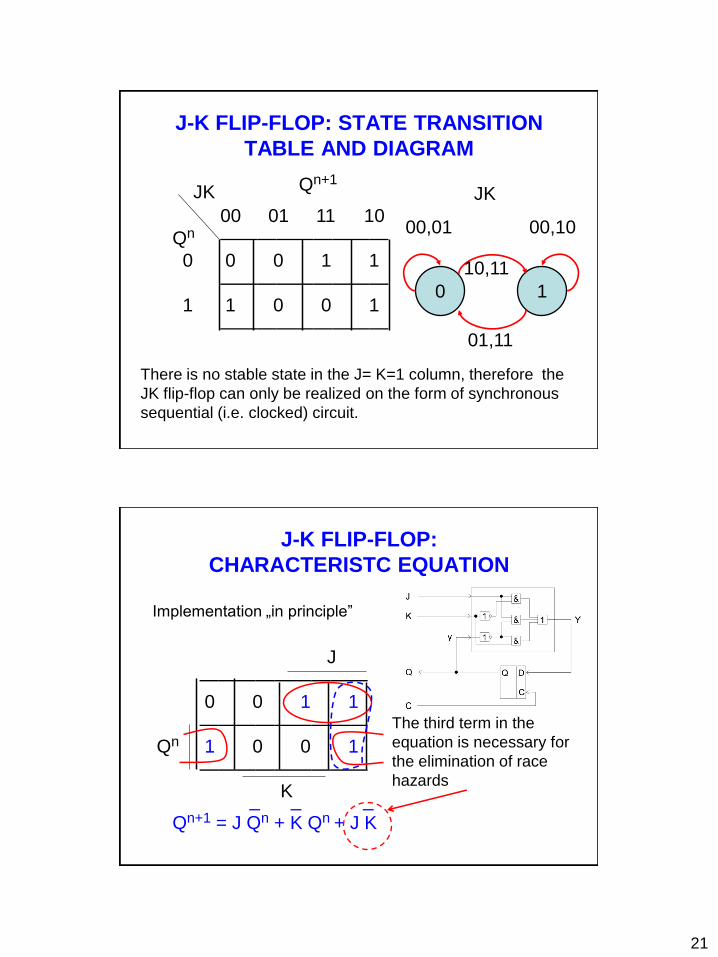
J-K FLIP-FLOP: STATE TRANSITION
TABLE AND DIAGRAM
00 01 11 10
Qn —————————
0 0 0 1 1
—————————
1 1 0 0 1
—————————
JK
0 1
JK
00,01 00,10
10,11
01,11
Qn+1
There is no stable state in the J= K=1 column, therefore the
JK flip-flop can only be realized on the form of synchronous
sequential (i.e. clocked) circuit.
J-K FLIP-FLOP:
CHARACTERISTC EQUATION
J
—————————
0 0 1 1
—————————
Qn 1 0 0 1
—————————
K _ _ _
Qn+1 = J Qn + K Qn + J K
The third term in the
equation is necessary for
the elimination of race
hazards
Implementation „in principle”
22
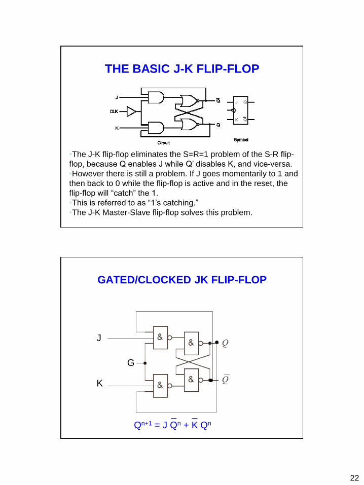
THE BASIC J-K FLIP-FLOP
•The J-K flip-flop eliminates the S=R=1 problem of the S-R flip-
flop, because Q enables J while Q’ disables K, and vice-versa.
•However there is still a problem. If J goes momentarily to 1 and
then back to 0 while the flip-flop is active and in the reset, the
flip-flop will “catch” the 1.
•This is referred to as “1’s catching.”
•The J-K Master-Slave flip-flop solves this problem.
GATED/CLOCKED JK FLIP-FLOP
J
K
G
_ _
Qn+1 = J Qn + K Qn
23
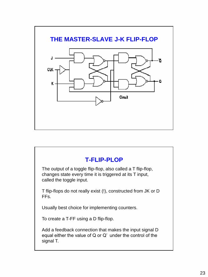
THE MASTER-SLAVE J-K FLIP-FLOP
T-FLIP-PLOP
The output of a toggle flip-flop, also called a T flip-flop,
changes state every time it is triggered at its T input,
called the toggle input.
T flip-flops do not really exist (!), constructed from JK or D
FFs.
Usually best choice for implementing counters.
To create a T-FF using a D flip-flop.
Add a feedback connection that makes the input signal D
equal either the value of Q or Q’ under the control of the
signal T.
24
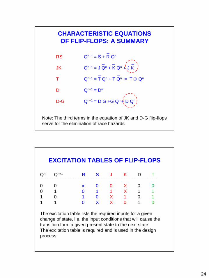
CHARACTERISTIC EQUATIONS
OF FLIP-FLOPS: A SUMMARY
_
RS Qn+1 = S + R Qn
_ _ _
JK Qn+1 = J Qn + K Qn + J K
_ _
T Qn+1 = T Qn + T Qn = T Qn
D Qn+1 = Dn
_
D-G Qn+1 = D G +G Qn + D Qn
Note: The third terms in the equation of JK and D-G flip-flops
serve for the elimination of race hazards
EXCITATION TABLES OF FLIP-FLOPS
Qn Qn+1 R S J K D T
¯¯¯¯¯¯¯¯¯¯¯¯¯¯¯¯¯¯¯¯¯¯¯¯¯¯¯¯¯¯¯¯¯¯¯¯¯¯¯¯¯¯¯¯¯¯
0 0 x 0 0 X 0 0
0 1 0 1 1 X 1 1
1 0 1 0 X 1 0 1
1 1 0 X X 0 1 0
The excitation table lists the required inputs for a given
change of state, i.e. the input conditions that will cause the
transition form a given present state to the next state.
The excitation table is required and is used in the design
process.
25
SUMMARY OF FLIP-FLOP TYPES
S=R=1 not
allowed
Most versatile
type
Most simple
Gated (DG)
Copies input to
output
Complements
output if activated
IMPLEMENTATION OF FLIP-FLOPS:
SOME PRACTCAL ASPECTS
• In the popular CMOS and TTL logic families T flip-flop is
not available. It should be build on the basis of an other
type of flip-flop.
• TTL, CMOS: basically JK and D flip-flops.
• PLA, PLD: only D flip-flop (!), the JK flip-flop should be
implemented by additional circuitry.
• RS flip-flop: in TTL it is based on NAND gates, in CMOS
it is based on NOR gates.
26
APPLICATION OF FLIP-FLOPS: SOME
PRACTICAL ASPECTS
• T flip-flops are well suited for straightforward binary
counters.
But may yield worst gate and pin counts.
• No reason to choose RS over JK FFs: it is a proper subset
of JK. RS FFs don’t exist anyway.
Tend to yield best choice for packaged logic where gate
count is the key.
• D FFs yield simplest design procedure. In many cases
give the best pin count.
D storage devices are very transistor efficient in VLSI.
Best choice where area/pin count is the key.
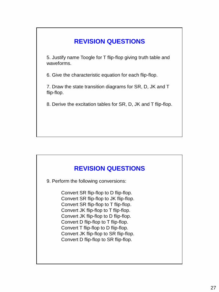
REVISION QUESTIONS
1. What do you mean by sequential circuit? Explain with
the help of a block diagram.
2. Give the comparison and explain the differences
between combinational and sequential circuits.
3. Give the comparison and explain the differences
between synchronous and asynchronous sequential
circuits.
4. What is the difference in the operation of edge-triggered
FFs and master slave FFs.
27
REVISION QUESTIONS
5. Justify name Toogle for T flip-flop giving truth table and
waveforms.
6. Give the characteristic equation for each flip-flop.
7. Draw the state transition diagrams for SR, D, JK and T
flip-flop.
8. Derive the excitation tables for SR, D, JK and T flip-flop.
REVISION QUESTIONS
9. Perform the following conversions:
Convert SR flip-flop to D flip-flop.
Convert SR flip-flop to JK flip-flop.
Convert SR flip-flop to T flip-flop.
Convert JK flip-flop to T flip-flop.
Convert JK flip-flop to D flip-flop.
Convert D flip-flop to T flip-flop.
Convert T flip-flop to D flip-flop.
Convert JK flip-flop to SR flip-flop.
Convert D flip-flop to SR flip-flop.
28
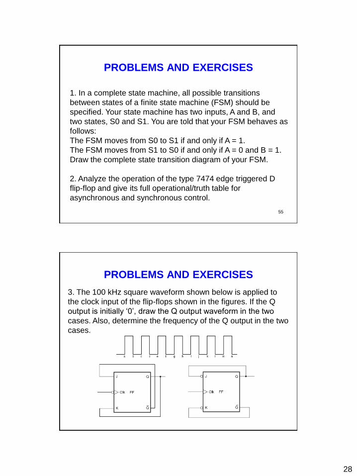
PROBLEMS AND EXERCISES
55
1. In a complete state machine, all possible transitions
between states of a finite state machine (FSM) should be
specified. Your state machine has two inputs, A and B, and
two states, S0 and S1. You are told that your FSM behaves as
follows:
The FSM moves from S0 to S1 if and only if A = 1.
The FSM moves from S1 to S0 if and only if A = 0 and B = 1.
Draw the complete state transition diagram of your FSM.
2. Analyze the operation of the type 7474 edge triggered D
flip-flop and give its full operational/truth table for
asynchronous and synchronous control.
PROBLEMS AND EXERCISES
3. The 100 kHz square waveform shown below is applied to
the clock input of the flip-flops shown in the figures. If the Q
output is initially ‘0’, draw the Q output waveform in the two
cases. Also, determine the frequency of the Q output in the two
cases.
29
END OF LECTURE ON
FLIP-FLOPS
Supplement follows
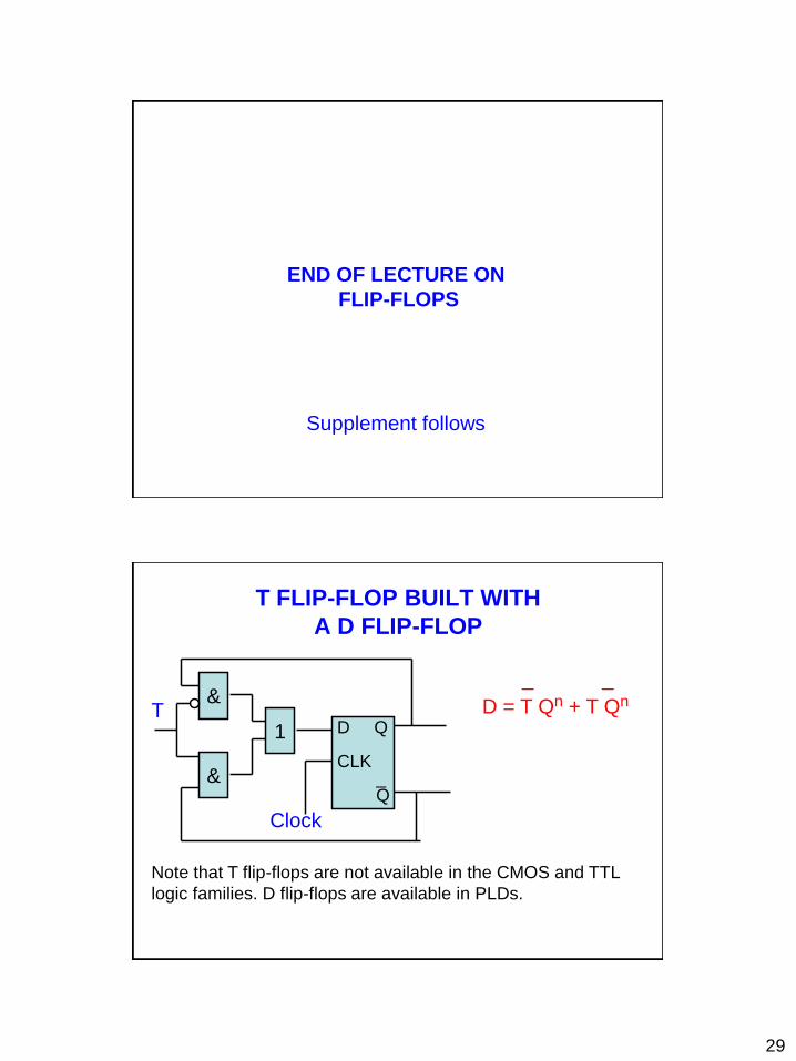
T FLIP-FLOP BUILT WITH
A D FLIP-FLOP
D Q CLK _ Q
&
&
1
Clock
T
_ _
D = T Qn + T Qn
Note that T flip-flops are not available in the CMOS and TTL
logic families. D flip-flops are available in PLDs.
30
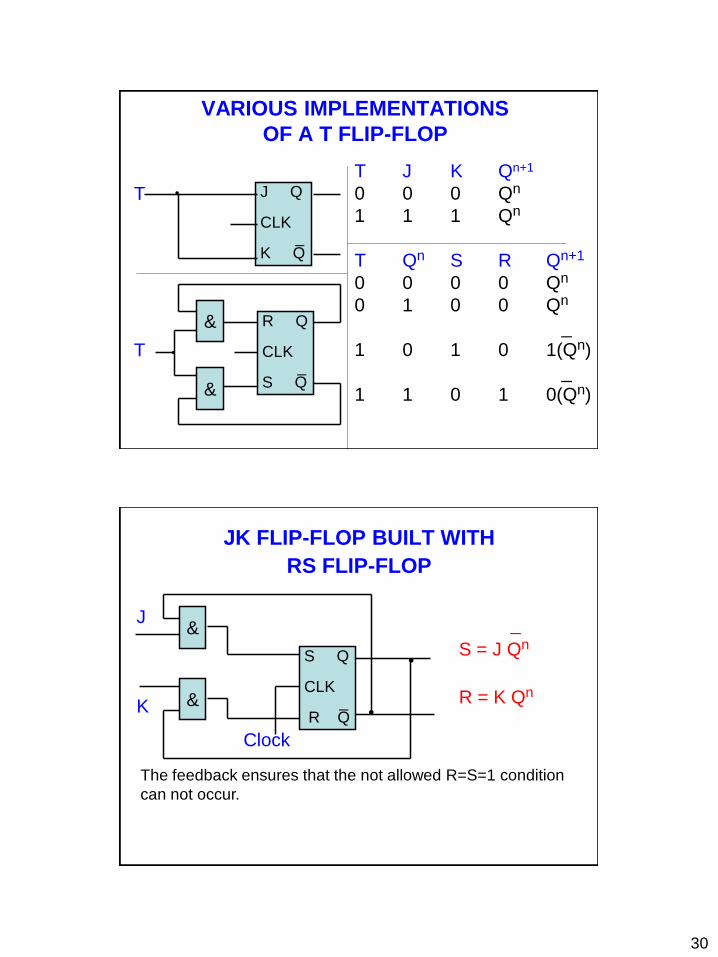
VARIOUS IMPLEMENTATIONS
OF A T FLIP-FLOP
J Q CLK _ K Q
R Q CLK _ S Q
&
T
T
&
T J K Qn+1
0 0 0 Qn
1 1 1 Qn
T Qn S R Qn+1
0 0 0 0 Qn
0 1 0 0 Qn
_
1 0 1 0 1(Qn)
_
1 1 0 1 0(Qn)
JK FLIP-FLOP BUILT WITH
RS FLIP-FLOP
S Q CLK _ R Q
&
&
Clock
J
K
•
•
_
S = J Qn
R = K Qn
The feedback ensures that the not allowed R=S=1 condition
can not occur.
31
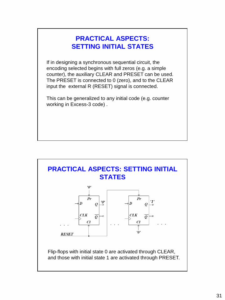
PRACTICAL ASPECTS:
SETTING INITIAL STATES
If in designing a synchronous sequential circuit, the
encoding selected begins with full zeros (e.g. a simple
counter), the auxiliary CLEAR and PRESET can be used.
The PRESET is connected to 0 (zero), and to the CLEAR
input the external R (RESET) signal is connected.
This can be generalized to any initial code (e.g. counter
working in Excess-3 code) .
PRACTICAL ASPECTS: SETTING INITIAL
STATES
Flip-flops with initial state 0 are activated through CLEAR,
and those with initial state 1 are activated through PRESET.
32
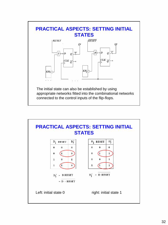
PRACTICAL ASPECTS: SETTING INITIAL
STATES
The initial state can also be established by using
appropriate networks fitted into the combinational networks
connected to the control inputs of the flip-flops.
PRACTICAL ASPECTS: SETTING INITIAL
STATES
Left: initial state 0 right: initial state 1
33
SUMMARY OF SOME ASPECTS
OF FLIP-FLOPS
Development of D flip-flop
Level-sensitive is used in custom ICs
Edge-triggered used in programmable logic deices
Good choice for data storage register
Historically JK flip-flop was popular but now never used
Similar to RS but wit 11 used to toggle output
Good in days of TTL/SSI (more complex input function)
Not a good choice for PALs/PLAs as it requires two inputs
Can always be implemented using D flip-flops
Preset and clear inputs are highly desirable on flip-flops
Used at start-up or to reset systems to a known state
SUMMARY OF SOME ASPECTS
OF FLIP-FLOPS
RS clocked latch:
Used as storage element in narrow width clocked systems
Its use is not recommended!
However fundamental building block of other flip-flop types
JK flip-flop:
Versatile building block
Can be used to implement D and T flip-flops
Usually requires least amount of logic to implement f(In, Q)
But has two inputs with increase wiring complexity
D flip-flops:
Minimizes wires, much preferred in VLSI technologies
Simplest design technique
Best choice for storage registers
T flip-flops:
Don’t really exist, constructed from JK flip-flops
Usually best choice for implementing counters