Embed Size (px)
Citation preview
G
I
Ps
TC
a
ARAA
KPSN
1
dat[(ioirieaitsikohsbe
(t
0h
ARTICLE IN PRESS Model
JLEO-53502; No. of Pages 4
Optik xxx (2013) xxx– xxx
Contents lists available at ScienceDirect
Optik
jou rn al homepage: www.elsev ier .de / i j leo
hotonic band gap in a one-dimensional periodic structure withemiconductor metamaterial in the near infrared
ingting Tangollege of Optoelectronic Technology, Chengdu University of Information Technology, Chengdu 610225, China
r t i c l e i n f o
rticle history:eceived 3 January 2013
a b s t r a c t
We construct a one-dimensional photonic crystal (1DPC) by use of semiconductor metamaterial in thenear infrared which is composed of Al-doped ZnO (AZO) and ZnO and dielectric material. The expressions
ccepted 20 May 2013vailable online xxx
eywords:hotonic crystalemiconductor metamaterial
of transmittance and field distribution are deduced by transfer matrix method, and the dispersion curvesof anisotropic permittivity of semiconductor metamaterial are analyzed at different ratio of AZO andZnO. At last simulation results are given to analyze the influence of thickness of dielectric material andincident angle on the transmittance of the proposed PC.
© 2013 Elsevier GmbH. All rights reserved.
ear infrared
. Introduction
Photonic crystals (PCs) are artificial materials with periodicallyielectric modulated function, and they have received considerablettention in recent years because of their property for stopping pho-ons with forbidden frequencies from propagating in the structures1,2], and these forbidden frequencies are call photonic band gapPBG). Metamaterial with negative permeability and/or permittiv-ty is another type of artificial composite [3–5] with a large numberf unusual electromagnetic properties, such as negative refractivendex, antiparallel group and phase velocities. It can be used toealize special PBGs, such as single-negative gaps (SNG) [6,7] orig-nated from the multilayered periodic structures with isotropicpsilon-negative (ENG) and mu-negative (MNG) materials. In 2001,rtificial metamaterials with negative refractive index was real-zed by periodic arrays of split ring resonators and wire strips inhe microwave regime [4]. After this, metamaterial received inten-ive interest within the scientific community, and was realized innfrared field. A research team in Princeton University reported aind of semiconductor metamaterial in mid-infrared field [8] basedn the strongly anisotropy of the dielectric response, and does notave any magnetic response. Recently Naik reported a new kind ofemiconductor metamaterial in near infrared field, which is formedy depositing 16 alternating layers of Al-doped ZnO (AZO) and ZnO,ach about 60 nm thick, on a silicon substrate [9].
Please cite this article in press as: T. Tang, Photonic band gap in a one-dimnear infrared, Optik - Int. J. Light Electron Opt. (2013), http://dx.doi.org/10
In this paper, we propose and demonstrate a one-dimensional1D) PC in a layered system containing the above semiconduc-or metamaterial and dielectric material. Transfer matrix method
E-mail address: [email protected]
030-4026/$ – see front matter © 2013 Elsevier GmbH. All rights reserved.ttp://dx.doi.org/10.1016/j.ijleo.2013.05.109
is used to analyze the theoretical model, and simulations aboutinfluence of dielectric thickness and semiconductor metamaterialconfiguration on the properties of PBG are also given.
2. Model and theory analysis
We consider a 1DPC created by alternating layers of isotropicdielectric material (A) and semiconductor metamaterial (B) mate-rial as (AB)N, where N is the period number. They are characterizedby εA and �A in layer A, and
εB =
⎛⎜⎝
ε‖ 0 0
0 ε‖ 0
0 0 ε⊥
⎞⎟⎠
and �B in layer B, respectively. The thickness of layer A and B aredenoted by dA and dB.
In the same layer, the electric and magnetic fields at any twopositions z and z + �z can be related to each other by a transfermatrix [6]:
Mj(�z) =(
cos(kjz�z) i sin(kj
z�z)/qj
iqj sin(kjz�z) cos(kj
z�z)
)j = (A, B) (1)
where k = k sin � and � is the incident angle with +z direc-
ensional periodic structure with semiconductor metamaterial in the.1016/j.ijleo.2013.05.109
x 0
tion. For TE wave, kAz =√
εA�Ak20 − k2
x , kBz =√
ε‖�Bk20 − k2
x , qA =kA
z /�Ak0 and qB = kBz /�Bk0. For TM wave, kA
z =√
εA�Ak20 − k2
x , kBz =√
ε‖�Bk20 − ε‖k2
x /ε⊥, qA = kAz /εAk0 and qB = kB
z /ε‖k0.
ING Model
I
2 xxx (2
t
t
w
Mm
Tp
Q
o
Q
t
3m
roDtfim
ε
ε
ε
ε
ε
Fe
� ≤ 2.057 �m, we can get ε⊥ < 0 and ε‖ > 0 as shown in Fig. 1(d),and in this case the semiconductor metamtaerial exhibits negativerefraction property. We choose N = 4, � = �/6, dB = 0.96 �m, εA = 2.5and �A = 1, and the corresponding transmittance in the periodic
ARTICLEJLEO-53502; No. of Pages 4
T. Tang / Optik
Then, the transmission coefficient t can be obtained from theransfer matrix:
= 2p
(M11 + M12p)p + M21 + M22p(2)
here Mij (i,j = 1, 2) is the matrix elements of (M1M2)N. Here
1 = MA(dA), M1 = MB(dB) and p =√
k20 − k2
x /k0. The power trans-ittance is determined by T = tt*.
We assume that electric field of the incident side E0 =[
10
]for
E waves and the electric field in layer A of the (n + 1)th (n < N)eriod is determined by EA(z) = QA(1, 1), where
A = MA(z − n(dA + dB))(M2M1)nE1. (3)
The electric field in layer B of the (n + 1)th (n < N) period isbtained by EB(z) = QB(1, 1), where
B = MB(z − n(dA + dB) − dA)M1(M2M1)nE1. (4)
The corresponding expressions for TM waves can be deduced byhe same method.
. Photonic crystal containing semiconductoretamaterial
According to the description about semiconductor metamate-ial composed of ZnO and Al-doped ZnO (AZO) in Ref. [9], theptical constants of the individual layers were extracted using arude + Lorentz model for AZO and a Lorentz model for ZnO, and
he permeability of ZnO is almost unchanged in the near infraredeld. Here we make use of εm(dm) and εd(dd) to demote the per-ittivity (thickness) of AZO and ZnO, respectively. Thus we assume
m1(f ) = 1 −f 2mp1 − f 2
mo1
f 2 − f 2mo1
(5)
m2 = 1 −f 2mp2
f 2(6)
m(f ) = εm1(f ) + εm2(f ) (7)
Please cite this article in press as: T. Tang, Photonic band gap in a one-dimnear infrared, Optik - Int. J. Light Electron Opt. (2013), http://dx.doi.org/10
d = 4 (8)
‖ = hεm + (1 − h)εd (9)
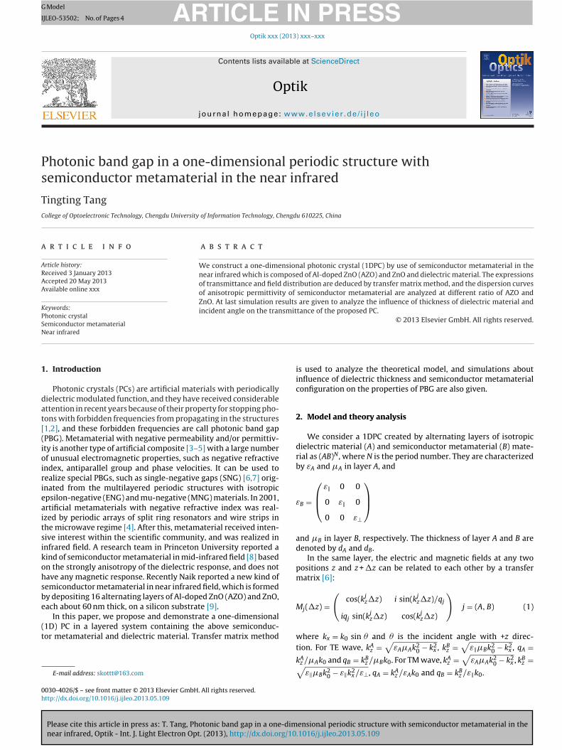
ig. 1. ε‖ and ε⊥ of semiconductor when the thicknesses of AZO and ZnO are differ-nt.
PRESS013) xxx– xxx
ε−1⊥ = hε−1
m + (1 − h)ε−1d
(10)
h = dm
dm + dd(11)
Here we choose fmp1 = 180 THz, fmp2 = 150 THz and fmo1 =80 THz, and the semiconductor metamaterial is nonmagnetic(�B = 1). Based on the above configuration, the ε‖ and ε⊥ are shownin Fig. 1 when the thicknesses of AZO and ZnO are different. As thetotal thickness of a heterostructure period is 60 nm, we choose (a)dm = 35 nm; dd = 25 nm, (b) dm = 40 nm; dd = 20 nm, (c) dm = 45 nm;dd = 15 nm and (d) dm = 50 nm; dd = 10 nm. We can find that withthe increase of dm/dd, ε‖ is decreasing while ε⊥ is increasing. InFig. 1(d), when � < 1.792 �m, we can get ε⊥ > 0 and ε‖ > 0; when1.792 �m ≤ � ≤ 2.057 �m, we can get ε⊥ < 0 and ε‖ > 0; when� > 2.057 �m, we can get ε⊥ < 0 and ε‖ < 0. In what following,we take into account two latter cases to discuss the PBG in theperiodic structure.
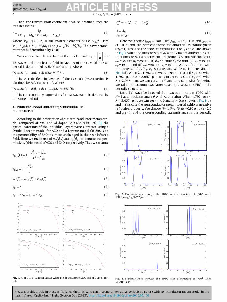
Let a TM wave be injected from vacuum into the 1DPC withN = 4 at an incident angle � with +z direction. When 1.792 �m ≤
ensional periodic structure with semiconductor metamaterial in the.1016/j.ijleo.2013.05.109
Fig. 2. Transmittances through the 1DPC with a structure of (AB)A when1.792 �m ≤ � ≤ 2.057 �m.
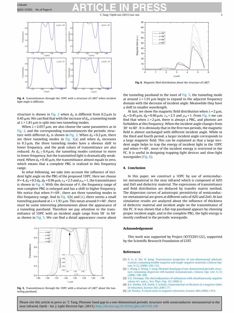
Fig. 3. Transmittances through the 1DPC with a structure of (AB)4 when� > 2.057 �m.
ARTICLE IN PRESSG Model
IJLEO-53502; No. of Pages 4
T. Tang / Optik xxx (2013) xxx– xxx 3
1.9 1.92 1.94 1.960
0.2
0.4
0.6
0.8
1
1.9 1.92 1.94 1.960
0.2
0.4
0.6
0.8
1
1.9 1.92 1.94 1.960
0.2
0.4
0.6
0.8
1
1.88 1.9 1.92 1.94 1.960
0.2
0.4
0.6
0.8
1
Transmittance
Transmittance
Transmittanc
ransmittance
μm μm
μm μm
69a 60 b
51c 45d
Fl
s0a
Ftatlrtewr
dNinWttmama
Fn
ig. 4. Transmittances through the 1DPC with a structure of (AB)4 when incidentight angle is different.
tructure is shown in Fig. 2 when dA is different from 0.2 �m to.45 �m. We can find that with the increase of dA, a tunneling modet � = 1.81 �m is split into two tunneling modes.
When � > 2.057 �m, we also choose the same parameters as inig. 2, and the corresponding transmittancein the periodic struc-ure with different dA is shown in Fig. 3. When dA = 0.2 �m, therere three tunneling modes in Fig. 3(a) and when dA increaseso 0.3 �m, the three tunneling modes have a obvious shift toower frequency, and the peak values of transmittance are alsoeduced. As dA ≥ 0.4 �m, the tunneling modes continue to moveo lower frequency, but the transmitted light is dramatically weak-ned. When dA = 0.45 �m, the transmittance almost equals to zero,hich means that a complete PBG is realized in this frequency
ange.In what following, we take into account the influence of inci-
ent light angle on the PBG of the proposed 1DPC. Here we choose = 4, dA = 0.5 dB, dB = 0.96 �m, εA = 2.5 and �A = 1, the transmittance
s shown in Fig. 4. With the decrease of �, the frequency range ofon-complete PBG is enlarged and has a shift to higher frequency.e notice that when � = 69◦, there are three tunneling modes in
his frequency range. And in Fig. 4(b) and (c), there seems a smallunneling passband at � = 1.91 �m. This mean around � = 60◦, there
ust be some interesting phenomenon about the appearance of
Please cite this article in press as: T. Tang, Photonic band gap in a one-dimnear infrared, Optik - Int. J. Light Electron Opt. (2013), http://dx.doi.org/10
tunneling passband. Therefore we pay attention to the trans-ittance of 1DPC with an incident angle range from 58◦ to 64◦
s shown in Fig. 5. We can find a detail appearance course about
ig. 5. Transmittances through the 1DPC with a structure of (AB)4 about the tun-eling passband.
[
[
[
[
[
Fig. 6. Magnetic filed distribution about the structure of (AB)4.
the tunneling passband in the inset of Fig. 5, the tunneling modeat around � = 1.91 �m begin to expand to the adjacent frequencydomain with the decrease of incident angle. Meanwhile they havea shift to smaller wavelength.
At last, we show the magnetic field distribution when � = 2 �m,dA = 0.45 �m, dB = 0.96 �m, εA = 2.5 and �A = 1. From Fig. 6 we canfind that when � = 2 �m, there is always a PBG, and photons areforbidden at this frequency. When the incident angle changes from30◦ to 60◦. It is obviously that in the first two periods, the magneticfield is almost unchanged with different incident angle. While inthe third and fourth period, a larger incident angle corresponds toa large magnetic field. This can be explained as that a large inci-dent angle helps to trap the energy of incident light in the 1DPCand when � = 60◦, most of the incident energy is restricted in thePC. It is useful in designing trapping-light devices and slow-lightwaveguides (Fig. 6).
4. Conclusion
In this paper, we construct a 1DPC by use of semiconduc-tor metamaterial in the near infrared which is composed of AZOand ZnO and dielectric material. The expressions of transmittanceand field distribution are deduced by transfer matrix method.The dispersion curves of anisotropic permittivity of semiconduc-tor metamaterial are given at different ratio of AZO and ZnO. At lastsimulation results are analyzed about the influence of thicknessof dielectric material and incident angle on the transmittance ofthe PC. It was shown that a flat-top passband appears by choosingproper incident angle, and in the complete PBG, the light energy ismostly confined in the periodic waveguide.
Acknowledgement
This work was supported by Project (KYTZ201122), supportedby the Scientific Research Foundation of CUIT.
References
1] X. Li, K. Xie, H. Jiang, Transmission properties of one-dimensional photoniccrustals containing double-negative and single-negative materials, Chinese Opt.Lett. 6 (2) (2008) 130–132.
2] L. Wang, Z. Wang, T. Sang, Photonic band gap of one-dimensional periodic struc-ture containing dispersive left-handed metamaterials, Chinese Opt. Lett. 6 (3)(2008) 198–200.
ensional periodic structure with semiconductor metamaterial in the.1016/j.ijleo.2013.05.109
3] V.G. Veselago, The electrodynamics of substances with simultaneously negativevalues of ε and �, Sov. Phys. Usp. 10 (1968) 4.
4] R.A. Shelby, D.R. Smith, S. Schultz, Experimental verification of a negative indexof refraction, Science 292 (2001) 77.
5] J.B. Pendry, A chiral route to negative refraction, Science 306 (2004) 1353.

ING Model
I
4 xxx (2
[
[
[
ARTICLEJLEO-53502; No. of Pages 4
T. Tang / Optik
6] H. Jiang, H. Chen, Y. ewen Zhang, Properties of one-dimensional photonic crystalscontaining single-negative materials, Phys. Rev. E 69 (2004) 066607.
Please cite this article in press as: T. Tang, Photonic band gap in a one-dimnear infrared, Optik - Int. J. Light Electron Opt. (2013), http://dx.doi.org/10
7] L.-G. Wang, H. Chen, S.-Y. Zhu, Omnidirectional gap and defect mode of one-dimensional photonic crystals with single-negative materials, Phys. Rev. B 70(2004) 245102.
8] A.J. Hoffman, L. Alekseyev, E.E. Narimanov, C. Gmachl, Negative refrac-tion in mid-infrared semiconductor metamaterials, in: Conference
[
PRESS013) xxx– xxx
on Lasers and Electro-Optics/Quantum Electronics and Laser ScienceConference and Photonic Applications Systems Technologies, OSA Tech-
ensional periodic structure with semiconductor metamaterial in the.1016/j.ijleo.2013.05.109
nical Digest (CD) (Optical Society of America, 2007), Paper QWH2,2007.
9] G.V. Naik, J. Liu, A.V. Kildishev, V.M. Shalaev, A. Boltasseva, Demonstration ofAl:ZnO as a plasmonic component for near-infrared metamaterials, Proc. Natl.Acad. Sci. 109 (23) (2012) 8834–8838.


![Silicon photonic platforms for mid-infrared applications · 2017-08-28 · Silicon photonic platforms for mid-infrared applications [Invited] TING HU,1 BOWEI DONG,1,2 XIANSHU LUO,1,*TSUNG-YANG](https://img.pdfslide.us/doc/110x75/5f2d7e81b1509f1a9a5435bd/silicon-photonic-platforms-for-mid-infrared-applications-2017-08-28-silicon-photonic.jpg)