Embed Size (px)
Citation preview
249
6Long-Wavelength Photonic Circuits
Goran Z. Mashanovich, Milan M. Milošević, Sanja Zlatanovic, Faezeh Gholami, Nikola Alic, Stojan Radic, Zoran Ikonic, Robert W. Kelsall, and Gunther Roelkens
CONTENTS
6.1 Introduction ........................................................................................................................250Goran Z. Mashanovich
6.2 Passive Devices for the Mid-Infrared Silicon Photonics .............................................. 251Milan M. Milošević and Goran Z. Mashanovich
6.2.1 Introduction ............................................................................................................ 2516.2.2 Silicon-on-Insulator ............................................................................................... 2516.2.3 Silicon-on-Sapphire ...............................................................................................2556.2.4 Silicon-on-Porous Silicon ......................................................................................2586.2.5 Chalcogenide Waveguides ................................................................................... 259
6.3 Nonlinear Effects in Silicon in the Mid-Infrared Region ............................................. 261Sanja Zlatanovic, Faezeh Gholami, Nikola Alic, and Stojan Radic
6.3.1 Introduction ............................................................................................................ 2616.3.2 Nonlinear Optics in Silicon .................................................................................. 2626.3.3 Two-Photon Absorption and Kerr Coefficient ................................................... 2636.3.4 Three-Photon Absorption ..................................................................................... 265
6.3.4.1 Free-Carrier Effects ................................................................................. 2656.3.5 Nonlinear Optical Processes in Silicon at Mid-Infrared Wavelengths .......... 266
6.3.5.1 Mid-IR Raman Amplification in Silicon .............................................. 2666.3.5.2 Self-Phase Modulation at Mid-IR Wavelengths .................................. 2676.3.5.3 Four-Wave Mixing and Parametric Amplification in the Mid-IR .... 269
6.3.6 Conclusion .............................................................................................................. 2716.4 Long Wavelength Silicon-Based Sources and Detectors .............................................. 271
Zoran Ikonic and Robert W. Kelsall
6.4.1 Introduction ............................................................................................................ 2716.4.2 Quantum Cascade Lasers ..................................................................................... 2716.4.3 Intracenter-Based Terahertz Lasers ..................................................................... 2736.4.4 Si/SiGe Quantum Well Infrared Photodetectors .............................................. 2756.4.5 SiGe Quantum Dot Detectors .............................................................................. 2766.4.6 Si/SiGe Micro-Bolometers .................................................................................... 2766.4.7 Conclusions .............................................................................................................277
6.5 Mid-Infrared Heterogeneous Integration ......................................................................277Gunther Roelkens
6.5.1 Introduction ............................................................................................................2776.5.2 Heterogeneous Integration—General ................................................................. 278
250 Handbook of Silicon Photonics
6.1 Introduction
Goran Z. Mashanovich
From the previous chapters, it could be seen that the majority of research effort in silicon photonics has been focused on the near-IR wavelength region. The long wave-length IR region, on the other hand, offers a plethora of possible applications ranging from sensing, medical diagnostics, and free space communications, to thermal imag-ing and IR countermeasures.
Silicon and germanium are transparent in a broad range of the long-wave IR and therefore can be used as photonics platforms in this wavelength region. Furthermore, the free carrier plasma dispersion effect should be stronger, two photon absorption is reduced, and more robust optical fibers are now available at longer wavelengths. In addition, the dimensional tolerances are more relaxed than in the near-IR. Moreover, III–V sources and detectors could be bonded on the silicon wafer, similar to approaches already demonstrated in the near-IR. Finally, silicon photonics, or group IV photonics, long wavelength platform is potentially low-cost and offers a possibility of photonic-electronic integration.
Recently, there has been an increased interest in long wavelength group IV photonics. This chapter presents recent results in the field. Possible waveguide structures have been suggested, and a review of silicon photonics passive structures designed for wavelengths ranging from 3.4 to 5.5 μm is given in Section 6.2. Different material platforms, such as silicon-on-insulator (SOI), silicon-on-sapphire, silicon on porous silicon and suspended silicon have been used.
A basic overview of optical nonlinearities and nonlinear material properties of sili-con in the mid-IR region, as well as the associated anisotropy and dispersion is given in Section 6.3. The main properties of silicon waveguides contributing to efficient nonlinear interactions, supported with recent experimental results are also presented, together with experimental demonstrations of the main nonlinear phenomena, including Raman ampli-fication, parametric amplification, and four-wave mixing.
Mid-IR and terahertz sources and detectors, including quantum cascade lasers, intracenter-based terahertz lasers, Si/SiGe quantum well, and quantum dot detectors, and micro-bolometers are discussed in Section 6.4. Finally, in Section 6.5, preliminary results on mid-IR heterogeneous integration of III–V and silicon are shown.
The long wavelength group IV photonics field is still in its infancy compared with the near-IR research, and there are a number of challenges that need to be overcome in the future before group IV photonic integrated circuits are employed in a host of applications offered by this spectral range. Nonetheless, significant progress has been made recently as described in this chapter. Therefore, we should expect to see some rather remarkable and exciting advances in this field in the near future.
6.5.3 Heterogeneous Integration—Detailed................................................................ 2796.5.4 Heterogeneously Integrated SWIR Photodetectors ..........................................2806.5.5 Heterogeneously Integrated SWIR Laser Diodes ............................................. 282
References ..................................................................................................................................... 282
251Long-Wavelength Photonic Circuits
6.2 Passive Devices for the Mid-Infrared Silicon Photonics
Milan M. Milošević and Goran Z. Mashanovich
6.2.1 Introduction
The fundamental challenge for mid-IR group IV photonics is the fact that the most popu-lar material platform in the NIR range, that of SOI, cannot be used in the majority of the MIR, due to high material losses of SiO2. Therefore, other waveguide structures need to be developed. Soref et al. proposed several waveguide structures suitable for mid- and long-IR spectral regions [1, 2]: Si rib-membrane waveguides, Si-on-Si3N4 (SON), Si-on-sapphire (SOS), Ge-on-Si, Ge-on-SOI, or GeSn-on-Si strip, and slot waveguides, or hollow wave-guides with Bragg or antiresonant cladding [1,2]. As waveguide dimensions scale with the wavelength, to reduce the dimensions and facilitate CMOS compatibility of MIR devices, plasmonic waveguides, and plasmonic waveguided components may prove to be a suit-able solution. It is expected that the plasmonic propagation loss will decrease significantly as the wavelength of operation is increased into the MIR, and far-IR [2]. In this section, we will present recently reported experimental data on passive MIR photonics devices.
6.2.2 Silicon-on-Insulator
It is well known from literature that silicon is relatively low loss (<2 dB/cm) for wave-lengths up to 8 μm, while there are several multiphonon absorption peaks at longer wave-lengths [1,2]. On the other hand, SiO2 optical loss rapidly increases beyond 3.6 μm, and therefore, SOI is not a suitable candidate for longer wavelengths [3].
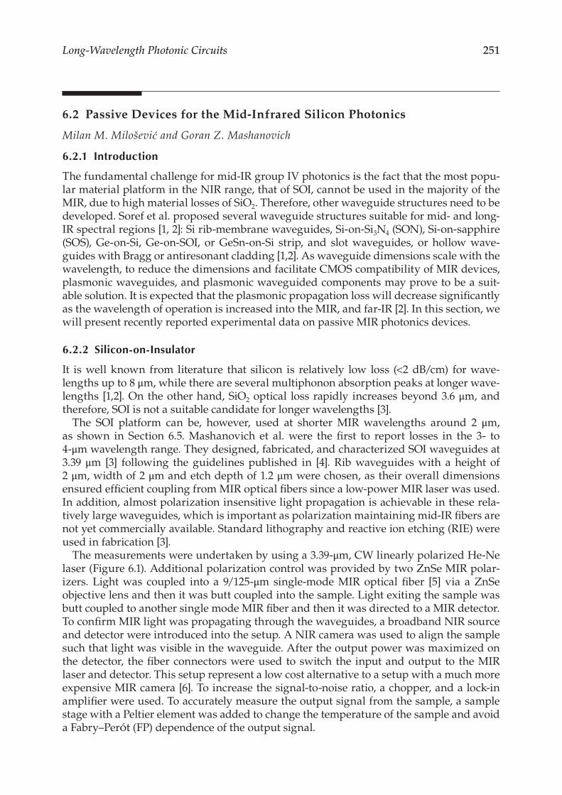
The SOI platform can be, however, used at shorter MIR wavelengths around 2 μm, as shown in Section 6.5. Mashanovich et al. were the first to report losses in the 3- to 4-μm wavelength range. They designed, fabricated, and characterized SOI waveguides at 3.39 μm [3] following the guidelines published in [4]. Rib waveguides with a height of 2 μm, width of 2 μm and etch depth of 1.2 μm were chosen, as their overall dimensions ensured efficient coupling from MIR optical fibers since a low-power MIR laser was used. In addition, almost polarization insensitive light propagation is achievable in these rela-tively large waveguides, which is important as polarization maintaining mid-IR fibers are not yet commercially available. Standard lithography and reactive ion etching (RIE) were used in fabrication [3].
The measurements were undertaken by using a 3.39-μm, CW linearly polarized He-Ne laser (Figure 6.1). Additional polarization control was provided by two ZnSe MIR polar-izers. Light was coupled into a 9/125-μm single-mode MIR optical fiber [5] via a ZnSe objective lens and then it was butt coupled into the sample. Light exiting the sample was butt coupled to another single mode MIR fiber and then it was directed to a MIR detector. To confirm MIR light was propagating through the waveguides, a broadband NIR source and detector were introduced into the setup. A NIR camera was used to align the sample such that light was visible in the waveguide. After the output power was maximized on the detector, the fiber connectors were used to switch the input and output to the MIR laser and detector. This setup represent a low cost alternative to a setup with a much more expensive MIR camera [6]. To increase the signal-to-noise ratio, a chopper, and a lock-in amplifier were used. To accurately measure the output signal from the sample, a sample stage with a Peltier element was added to change the temperature of the sample and avoid a Fabry–PerÓt (FP) dependence of the output signal.
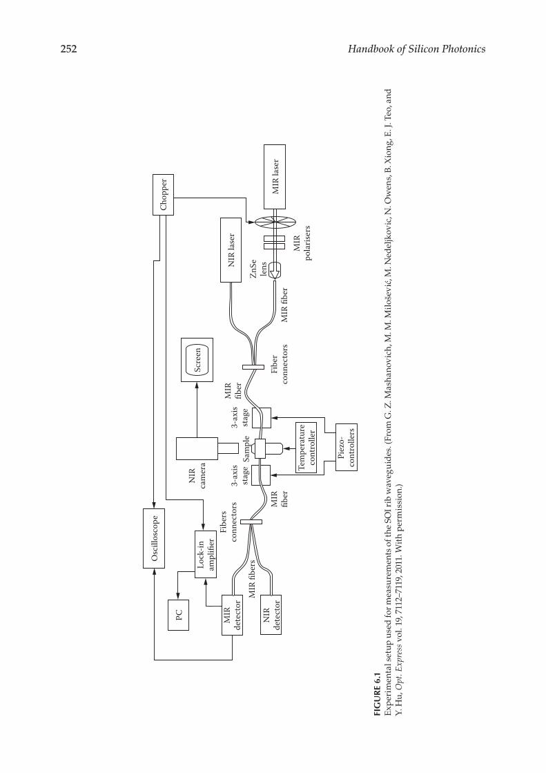
252 Handbook of Silicon Photonics
Osc
illos
cope
PC MIR
dete
ctor
NIR
dete
ctor
MIR
fibe
rs
Fibe
rsco
nnec
tors
NIR
cam
era
MIR
fiber
MIR
fiber
3-ax
isst
age
3-ax
isst
age
Sam
ple
Tem
pera
ture
cont
rolle
r
Fibe
rco
nnec
tors
MIR
fibe
r
Scre
en
NIR
lase
r
Cho
pper
MIR
lase
r
MIR
pola
riser
s
ZnSe
lens
Piez
o-co
ntro
llers
Lock
-inam
plifi
er
FIG
UR
E 6.
1E
xper
imen
tal s
etup
use
d fo
r m
easu
rem
ents
of t
he S
OI r
ib w
aveg
uid
es. (
From
G. Z
. Mas
hano
vich
, M. M
. Milo
ševi
ć, M
. Ned
eljk
ovic
, N. O
wen
s, B
. Xio
ng, E
. J. T
eo, a
nd
Y. H
u, O
pt. E
xpre
ss v
ol. 1
9, 7
112–
7119
, 201
1. W
ith
per
mis
sion
.)
253Long-Wavelength Photonic Circuits
The noise floor was more than 20 dB lower than the typical measured peak power and the total on chip loss was around 23 dB. The experimentally measured bend loss was 0.006 ± 0.002 dB for 90° bends with 200-μm radius.
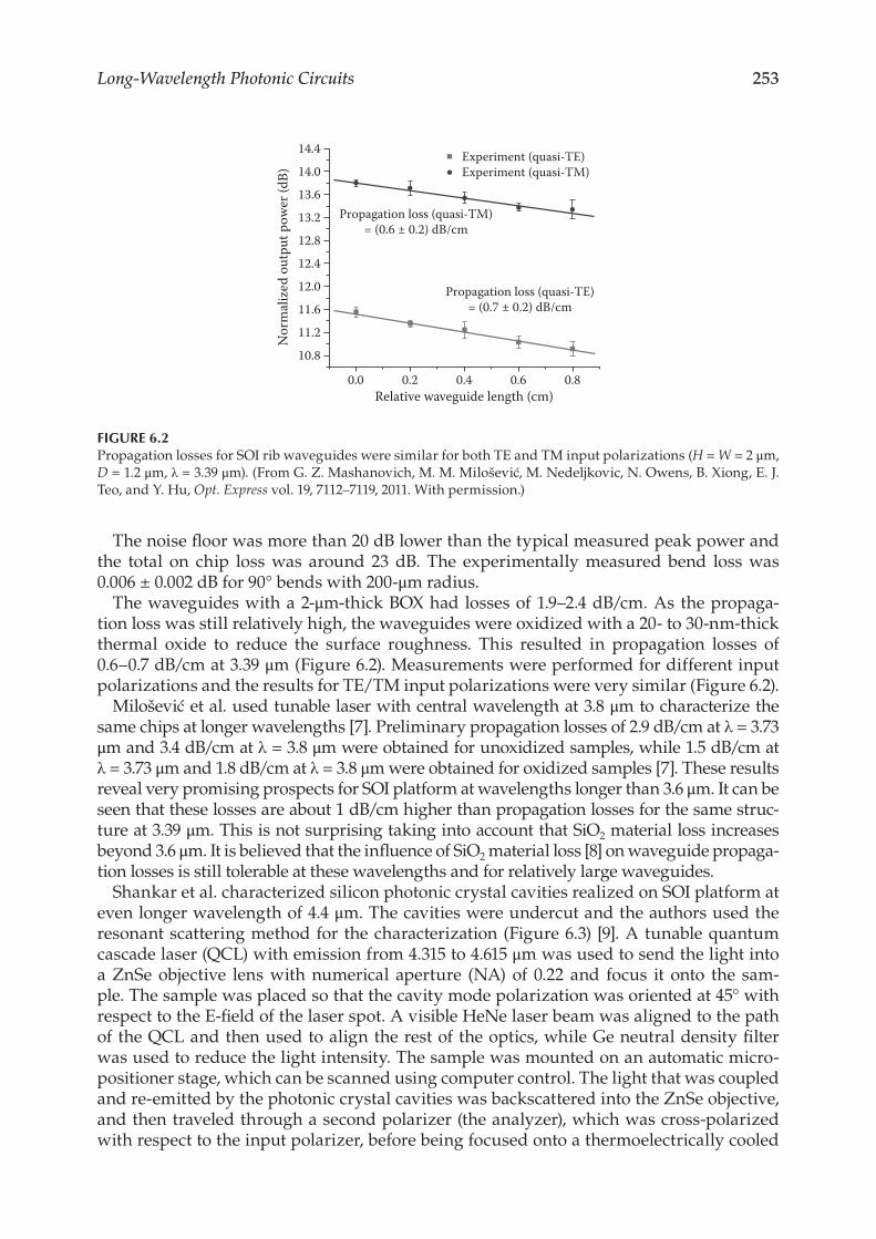
The waveguides with a 2-μm-thick BOX had losses of 1.9–2.4 dB/cm. As the propaga-tion loss was still relatively high, the waveguides were oxidized with a 20- to 30-nm-thick thermal oxide to reduce the surface roughness. This resulted in propagation losses of 0.6–0.7 dB/cm at 3.39 μm (Figure 6.2). Measurements were performed for different input polarizations and the results for TE/TM input polarizations were very similar (Figure 6.2).
Milošević et al. used tunable laser with central wavelength at 3.8 μm to characterize the same chips at longer wavelengths [7]. Preliminary propagation losses of 2.9 dB/cm at λ = 3.73 μm and 3.4 dB/cm at λ = 3.8 μm were obtained for unoxidized samples, while 1.5 dB/cm at λ = 3.73 μm and 1.8 dB/cm at λ = 3.8 μm were obtained for oxidized samples [7]. These results reveal very promising prospects for SOI platform at wavelengths longer than 3.6 μm. It can be seen that these losses are about 1 dB/cm higher than propagation losses for the same struc-ture at 3.39 μm. This is not surprising taking into account that SiO2 material loss increases beyond 3.6 μm. It is believed that the influence of SiO2 material loss [8] on waveguide propaga-tion losses is still tolerable at these wavelengths and for relatively large waveguides.
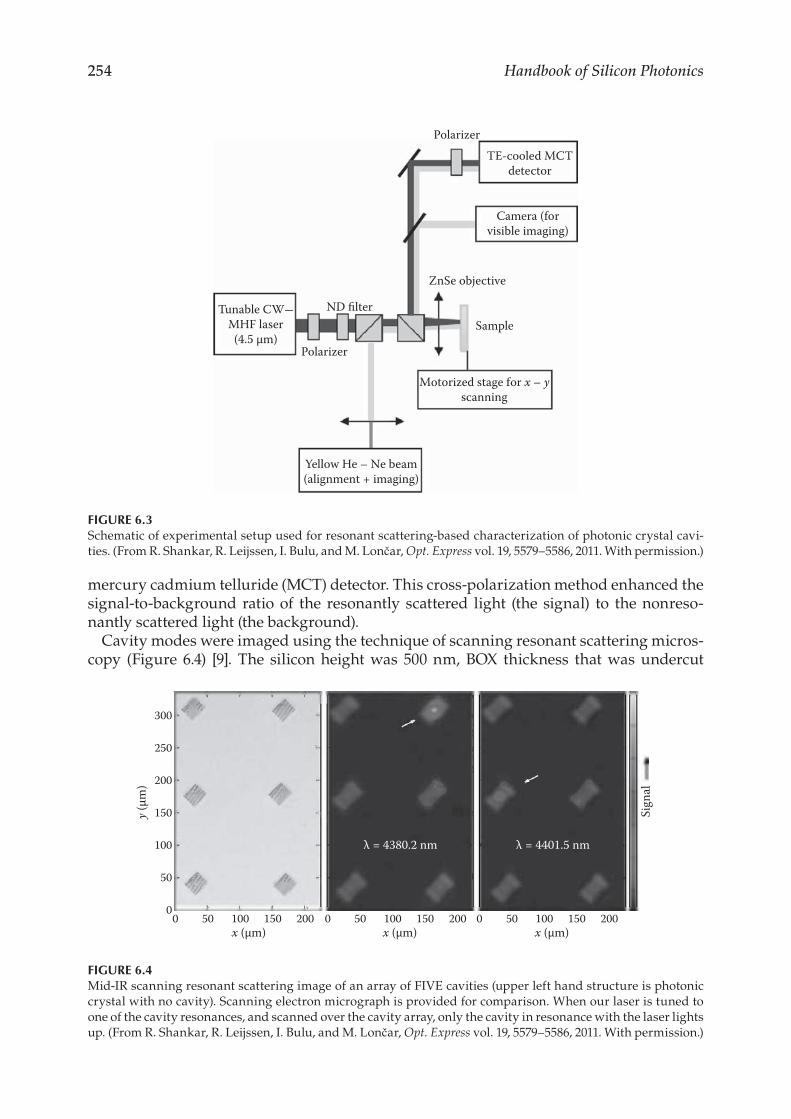
Shankar et al. characterized silicon photonic crystal cavities realized on SOI platform at even longer wavelength of 4.4 μm. The cavities were undercut and the authors used the resonant scattering method for the characterization (Figure 6.3) [9]. A tunable quantum cascade laser (QCL) with emission from 4.315 to 4.615 μm was used to send the light into a ZnSe objective lens with numerical aperture (NA) of 0.22 and focus it onto the sam-ple. The sample was placed so that the cavity mode polarization was oriented at 45° with respect to the E-field of the laser spot. A visible HeNe laser beam was aligned to the path of the QCL and then used to align the rest of the optics, while Ge neutral density filter was used to reduce the light intensity. The sample was mounted on an automatic micro-positioner stage, which can be scanned using computer control. The light that was coupled and re-emitted by the photonic crystal cavities was backscattered into the ZnSe objective, and then traveled through a second polarizer (the analyzer), which was cross-polarized with respect to the input polarizer, before being focused onto a thermoelectrically cooled
14.4 Experiment (quasi-TE)Experiment (quasi-TM)
Propagation loss (quasi-TM)= (0.6 ± 0.2) dB/cm
Propagation loss (quasi-TE)= (0.7 ± 0.2) dB/cm
14.0
13.6
13.2
12.8
12.4
12.0
11.6
11.2
10.8
0.0 0.2 0.4Relative waveguide length (cm)
Nor
mal
ized
out
put p
ower
(dB)
0.6 0.8
FIGURE 6.2Propagation losses for SOI rib waveguides were similar for both TE and TM input polarizations (H = W = 2 μm, D = 1.2 μm, λ = 3.39 μm). (From G. Z. Mashanovich, M. M. Milošević, M. Nedeljkovic, N. Owens, B. Xiong, E. J. Teo, and Y. Hu, Opt. Express vol. 19, 7112–7119, 2011. With permission.)
254 Handbook of Silicon Photonics
mercury cadmium telluride (MCT) detector. This cross-polarization method enhanced the signal -to-background ratio of the resonantly scattered light (the signal) to the nonreso-nantly scattered light (the background).
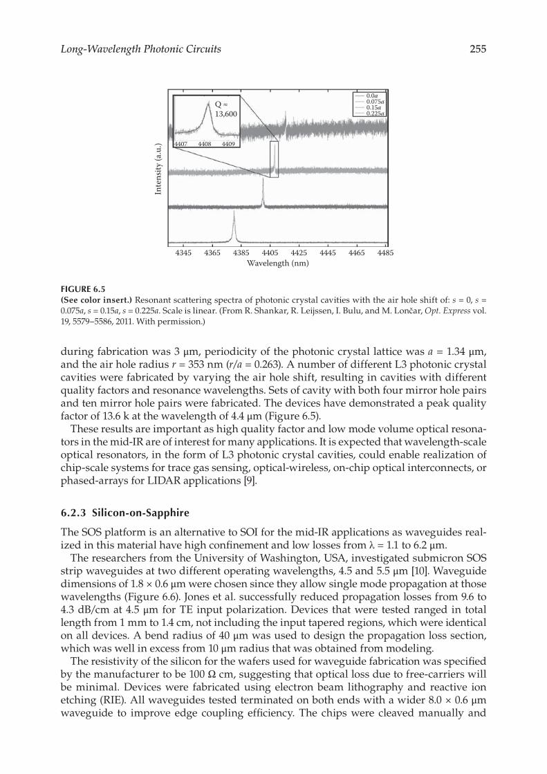
Cavity modes were imaged using the technique of scanning resonant scattering micros-copy (Figure 6.4) [9]. The silicon height was 500 nm, BOX thickness that was undercut
PolarizerTE-cooled MCT
detector
Camera (forvisible imaging)
Sample
ZnSe objective
Polarizer
Tunable CW—MHF laser(4.5 μm)
Motorized stage for x – yscanning
Yellow He – Ne beam(alignment + imaging)
ND filter
FIGURE 6.3Schematic of experimental setup used for resonant scattering-based characterization of photonic crystal cavi-ties. (From R. Shankar, R. Leijssen, I. Bulu, and M. Lončar, Opt. Express vol. 19, 5579–5586, 2011. With permission.)
300
250
200
y (μm
)
150
100
50
00 50 100 150 200 0 50 100 150 200 0 50 100 150 200
x (μm) x (μm)
λ = 4380.2 nm λ = 4401.5 nm
x (μm)
Sign
al
FIGURE 6.4Mid-IR scanning resonant scattering image of an array of FIVE cavities (upper left hand structure is photonic crystal with no cavity). Scanning electron micrograph is provided for comparison. When our laser is tuned to one of the cavity resonances, and scanned over the cavity array, only the cavity in resonance with the laser lights up. (From R. Shankar, R. Leijssen, I. Bulu, and M. Lončar, Opt. Express vol. 19, 5579–5586, 2011. With permission.)
255Long-Wavelength Photonic Circuits
during fabrication was 3 μm, periodicity of the photonic crystal lattice was a = 1.34 μm, and the air hole radius r = 353 nm (r/a = 0.263). A number of different L3 photonic crystal cavities were fabricated by varying the air hole shift, resulting in cavities with different quality factors and resonance wavelengths. Sets of cavity with both four mirror hole pairs and ten mirror hole pairs were fabricated. The devices have demonstrated a peak quality factor of 13.6 k at the wavelength of 4.4 μm (Figure 6.5).
These results are important as high quality factor and low mode volume optical resona-tors in the mid-IR are of interest for many applications. It is expected that wavelength-scale optical resonators, in the form of L3 photonic crystal cavities, could enable realization of chip-scale systems for trace gas sensing, optical-wireless, on-chip optical interconnects, or phased-arrays for LIDAR applications [9].
6.2.3 Silicon-on-Sapphire
The SOS platform is an alternative to SOI for the mid-IR applications as waveguides real-ized in this material have high confinement and low losses from λ = 1.1 to 6.2 μm.
The researchers from the University of Washington, USA, investigated submicron SOS strip waveguides at two different operating wavelengths, 4.5 and 5.5 μm [10]. Waveguide dimensions of 1.8 × 0.6 μm were chosen since they allow single mode propagation at those wavelengths (Figure 6.6). Jones et al. successfully reduced propagation losses from 9.6 to 4.3 dB/cm at 4.5 μm for TE input polarization. Devices that were tested ranged in total length from 1 mm to 1.4 cm, not including the input tapered regions, which were identical on all devices. A bend radius of 40 μm was used to design the propagation loss section, which was well in excess from 10 μm radius that was obtained from modeling.
The resistivity of the silicon for the wafers used for waveguide fabrication was specified by the manufacturer to be 100 Ω cm, suggesting that optical loss due to free-carriers will be minimal. Devices were fabricated using electron beam lithography and reactive ion etching (RIE). All waveguides tested terminated on both ends with a wider 8.0 × 0.6 μm waveguide to improve edge coupling efficiency. The chips were cleaved manually and
4345
4407 4408 4409
0.0a0.075a0.15a0.225a
Q ≈13,600
4365 4385 4405Wavelength (nm)
Inte
nsity
(a.u
.)
4425 4445 4465 4485
FIGURE 6.5(See color insert.) Resonant scattering spectra of photonic crystal cavities with the air hole shift of: s = 0, s = 0.075a, s = 0.15a, s = 0.225a. Scale is linear. (From R. Shankar, R. Leijssen, I. Bulu, and M. Lončar, Opt. Express vol. 19, 5579–5586, 2011. With permission.)
256 Handbook of Silicon Photonics
measured. The experimental setup used to measure these devices consisted of an Nd:YAG laser that drove an optical parameteric generator/difference frequency generator (OPG/DFG) (Figure 6.7). The OPG/DFG provided 30 ps pulses of IR light at a repetition rate of 50 Hz with pulse energies around 150 μJ. It was capable of producing linearly polarized
1.0 μm
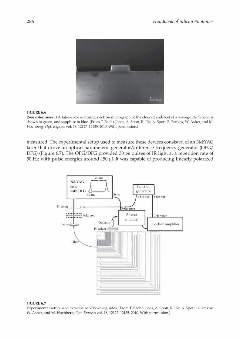
FIGURE 6.6(See color insert.) A false-color scanning electron micrograph of the cleaved endfacet of a waveguide. Silicon is shown in green, and sapphire in blue. (From T. Baehr-Jones, A. Spott, R. Ilic, A. Spott, B. Penkov, W. Asher, and M. Hochberg, Opt. Express vol. 18, 12127–12135, 2010. With permission.)
Lock-in amplifier
Boxcaramplifier
Functiongenerator
Nd-YAGlaserwith DFG
20 ms
30 ms Sync2 Hz out 2 Hz out
Reference
Reference
Detector
Polarizer
Polarizer
Shutter
Lens
Fiber
FIGURE 6.7Experimental setup used to measure SOS waveguides. (From T. Baehr-Jones, A. Spott, R. Ilic, A. Spott, B. Penkov, W. Asher, and M. Hochberg, Opt. Express vol. 18, 12127–12135, 2010. With permission.)
257Long-Wavelength Photonic Circuits
light from 2 to 9 μm, with 4.5 μm radiation used for testing. The wavelength of 4.5 μm was chosen as the fiber cut off at longer wavelengths, and it was impossible to achieve as great a dynamic range at other wavelengths due to decreased emission power and beam stability from the OPG/DFG. The laser was coupled through a polarizer into ZnSe lens and into a 9/125-μm single-mode MIR optical fiber. The output of the chip was coupled directly to free space and then into a detector. The boxcar amplifier was used to reject the signal during the times when the laser was not providing output. The signal-to-noise ratio was enhanced by mechanically chopping the laser at 2 Hz, and using a lock-in amplifier to detect the 2-Hz-modulated signal. This resulted in an overall signal-to-noise ratio of 85 dB and the insertion losses of 12 dB.
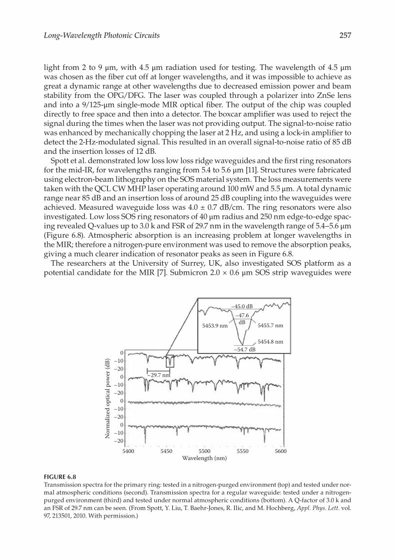
Spott et al. demonstrated low loss low loss ridge waveguides and the first ring resonators for the mid-IR, for wavelengths ranging from 5.4 to 5.6 μm [11]. Structures were fabricated using electron-beam lithography on the SOS material system. The loss measurements were taken with the QCL CW MHP laser operating around 100 mW and 5.5 μm. A total dynamic range near 85 dB and an insertion loss of around 25 dB coupling into the waveguides were achieved. Measured waveguide loss was 4.0 ± 0.7 dB/cm. The ring resonators were also investigated. Low loss SOS ring resonators of 40 μm radius and 250 nm edge-to-edge spac-ing revealed Q-values up to 3.0 k and FSR of 29.7 nm in the wavelength range of 5.4–5.6 μm (Figure 6.8). Atmospheric absorption is an increasing problem at longer wavelengths in the MIR; therefore a nitrogen-pure environment was used to remove the absorption peaks, giving a much clearer indication of resonator peaks as seen in Figure 6.8.
The researchers at the University of Surrey, UK, also investigated SOS platform as a potential candidate for the MIR [7]. Submicron 2.0 × 0.6 μm SOS strip waveguides were
0–10–20
0–10–20
0–10–20
–10–20
5400 5450
~29.7 nm
5453.9 nm
–45.0 dB–47.6
dB
–54.7 dB
5455.7 nm
5454.8 nm
5500Wavelength (nm)
Nor
mal
ized
opt
ical
pow
er (d
B)
5550 5600
0
FIGURE 6.8Transmission spectra for the primary ring: tested in a nitrogen-purged environment (top) and tested under nor-mal atmospheric conditions (second). Transmission spectra for a regular waveguide: tested under a nitrogen-purged environment (third) and tested under normal atmospheric conditions (bottom). A Q-factor of 3.0 k and an FSR of 29.7 nm can be seen. (From Spott, Y. Liu, T. Baehr-Jones, R. Ilic, and M. Hochberg, Appl. Phys. Lett. vol. 97, 213501, 2010. With permission.)
258 Handbook of Silicon Photonics
fabricated using standard lithography and RIE etching. The focused ion beam (FIB) with the beam current of 0.5 nA was used to trim waveguide facets. The resulting profile was improved dramatically thus facilitating efficient coupling to the SOS waveguides. The propagation losses of 3.6 dB/cm at 3.39 μm were achieved.
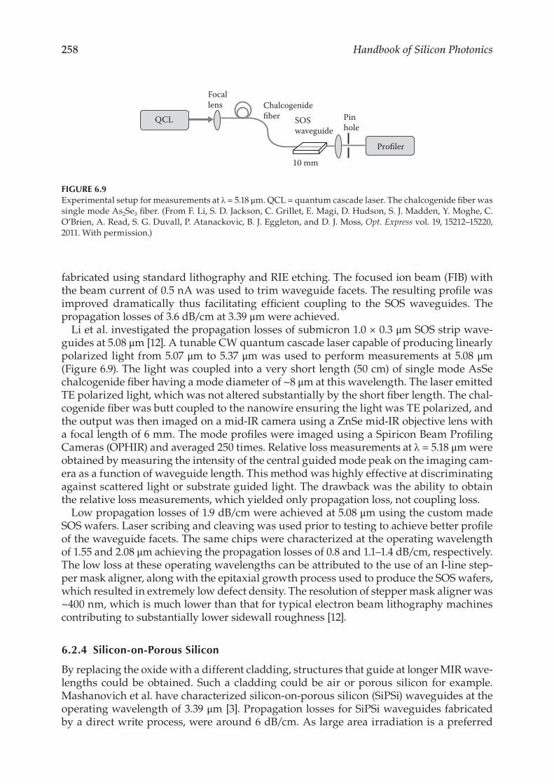
Li et al. investigated the propagation losses of submicron 1.0 × 0.3 μm SOS strip wave-guides at 5.08 μm [12]. A tunable CW quantum cascade laser capable of producing linearly polarized light from 5.07 μm to 5.37 μm was used to perform measurements at 5.08 μm (Figure 6.9). The light was coupled into a very short length (50 cm) of single mode AsSe chalcogenide fiber having a mode diameter of ~8 μm at this wavelength. The laser emitted TE polarized light, which was not altered substantially by the short fiber length. The chal-cogenide fiber was butt coupled to the nanowire ensuring the light was TE polarized, and the output was then imaged on a mid-IR camera using a ZnSe mid-IR objective lens with a focal length of 6 mm. The mode profiles were imaged using a Spiricon Beam Profiling Cameras (OPHIR) and averaged 250 times. Relative loss measurements at λ = 5.18 μm were obtained by measuring the intensity of the central guided mode peak on the imaging cam-era as a function of waveguide length. This method was highly effective at discriminating against scattered light or substrate guided light. The drawback was the ability to obtain the relative loss measurements, which yielded only propagation loss, not coupling loss.
Low propagation losses of 1.9 dB/cm were achieved at 5.08 μm using the custom made SOS wafers. Laser scribing and cleaving was used prior to testing to achieve better profile of the waveguide facets. The same chips were characterized at the operating wavelength of 1.55 and 2.08 μm achieving the propagation losses of 0.8 and 1.1–1.4 dB/cm, respectively. The low loss at these operating wavelengths can be attributed to the use of an I-line step-per mask aligner, along with the epitaxial growth process used to produce the SOS wafers, which resulted in extremely low defect density. The resolution of stepper mask aligner was ~400 nm, which is much lower than that for typical electron beam lithography machines contributing to substantially lower sidewall roughness [12].
6.2.4 Silicon-on-Porous Silicon
By replacing the oxide with a different cladding, structures that guide at longer MIR wave-lengths could be obtained. Such a cladding could be air or porous silicon for example. Mashanovich et al. have characterized silicon-on-porous silicon (SiPSi) waveguides at the operating wavelength of 3.39 μm [3]. Propagation losses for SiPSi waveguides fabricated by a direct write process, were around 6 dB/cm. As large area irradiation is a preferred
Focallens Chalcogenide
fiber SOSwaveguide
Pinhole
10 mm
Profiler
QCL
FIGURE 6.9Experimental setup for measurements at λ = 5.18 μm. QCL = quantum cascade laser. The chalcogenide fiber was single mode As2Se3 fiber. (From F. Li, S. D. Jackson, C. Grillet, E. Magi, D. Hudson, S. J. Madden, Y. Moghe, C. O’Brien, A. Read, S. G. Duvall, P. Atanackovic, B. J. Eggleton, and D. J. Moss, Opt. Express vol. 19, 15212–15220, 2011. With permission.)
259Long-Wavelength Photonic Circuits
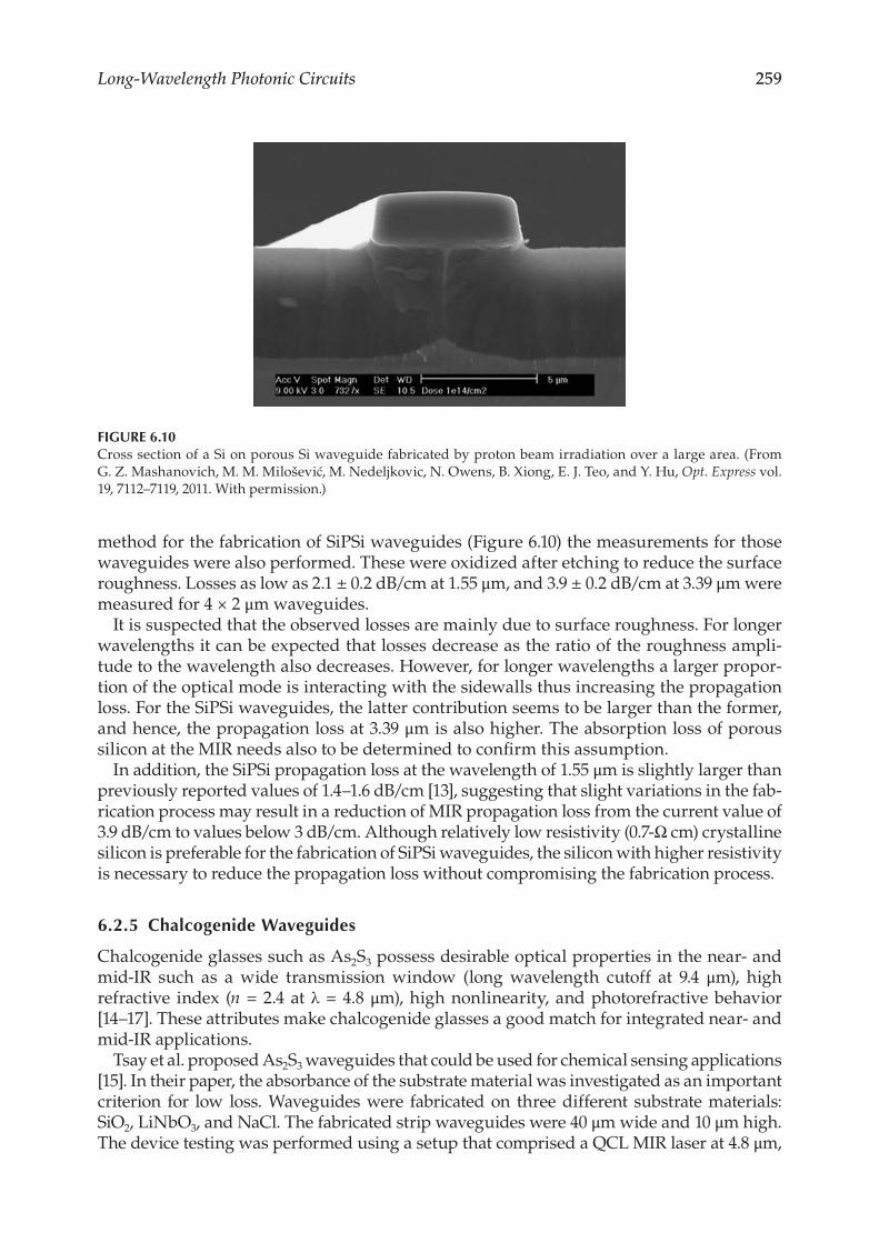
method for the fabrication of SiPSi waveguides (Figure 6.10) the measurements for those waveguides were also performed. These were oxidized after etching to reduce the surface roughness. Losses as low as 2.1 ± 0.2 dB/cm at 1.55 μm, and 3.9 ± 0.2 dB/cm at 3.39 μm were measured for 4 × 2 μm waveguides.
It is suspected that the observed losses are mainly due to surface roughness. For longer wavelengths it can be expected that losses decrease as the ratio of the roughness ampli-tude to the wavelength also decreases. However, for longer wavelengths a larger propor-tion of the optical mode is interacting with the sidewalls thus increasing the propagation loss. For the SiPSi waveguides, the latter contribution seems to be larger than the former, and hence, the propagation loss at 3.39 μm is also higher. The absorption loss of porous silicon at the MIR needs also to be determined to confirm this assumption.
In addition, the SiPSi propagation loss at the wavelength of 1.55 μm is slightly larger than previously reported values of 1.4–1.6 dB/cm [13], suggesting that slight variations in the fab-rication process may result in a reduction of MIR propagation loss from the current value of 3.9 dB/cm to values below 3 dB/cm. Although relatively low resistivity (0.7-Ω cm) crystalline silicon is preferable for the fabrication of SiPSi waveguides, the silicon with higher resistivity is necessary to reduce the propagation loss without compromising the fabrication process.
6.2.5 Chalcogenide Waveguides
Chalcogenide glasses such as As2S3 possess desirable optical properties in the near- and mid-IR such as a wide transmission window (long wavelength cutoff at 9.4 μm), high refractive index (n = 2.4 at λ = 4.8 μm), high nonlinearity, and photorefractive behavior [14–17]. These attributes make chalcogenide glasses a good match for integrated near- and mid-IR applications.
Tsay et al. proposed As2S3 waveguides that could be used for chemical sensing applications [15]. In their paper, the absorbance of the substrate material was investigated as an important criterion for low loss. Waveguides were fabricated on three different substrate materials: SiO2, LiNbO3, and NaCl. The fabricated strip waveguides were 40 μm wide and 10 μm high. The device testing was performed using a setup that comprised a QCL MIR laser at 4.8 μm,
FIGURE 6.10Cross section of a Si on porous Si waveguide fabricated by proton beam irradiation over a large area. (From G. Z. Mashanovich, M. M. Milošević, M. Nedeljkovic, N. Owens, B. Xiong, E. J. Teo, and Y. Hu, Opt. Express vol. 19, 7112–7119, 2011. With permission.)
260 Handbook of Silicon Photonics
–15.0
–17.0
–19.0
–21.0
–23.0
–25.0
–27.0
–29.00 0.1 0.2 0.3 0.4 0.5
Length (cm)
(a) (b)
NaCl6.2 dB/cm
LiNbO37.9 dB/cm
SiO29.4 dB/cm
LiNbO3(annealed)6.7 dB/cm
NaCl(annealed)4.5 dB/cm
NaCl(unannealed)
6.2 dB/cm
Length (cm)
Loss
(dB)
Loss
(dB)
0.6 0.7 0.8 0.9 1 0 0.1 0.2 0.3 0.4 0.5 0.6 0.7 0.8 0.9 1.0
–14.0
–16.0
–18.0
–20.0
–22.0
–24.0
–26.0
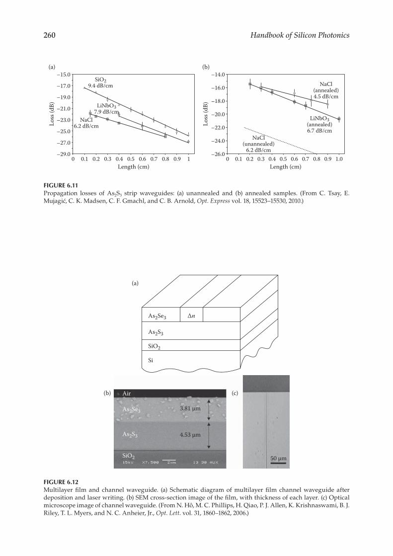
FIGURE 6.11Propagation losses of As2S3 strip waveguides: (a) unannealed and (b) annealed samples. (From C. Tsay, E. Mujagić, C. K. Madsen, C. F. Gmachl, and C. B. Arnold, Opt. Express vol. 18, 15523–15530, 2010.)
Air
As2Se3
As2Se3
(a)
Δn
As2S3
SiO2
Si
3.81 μm
4.53 μm
50 μm
(b) (c)
As2S3
SiO2
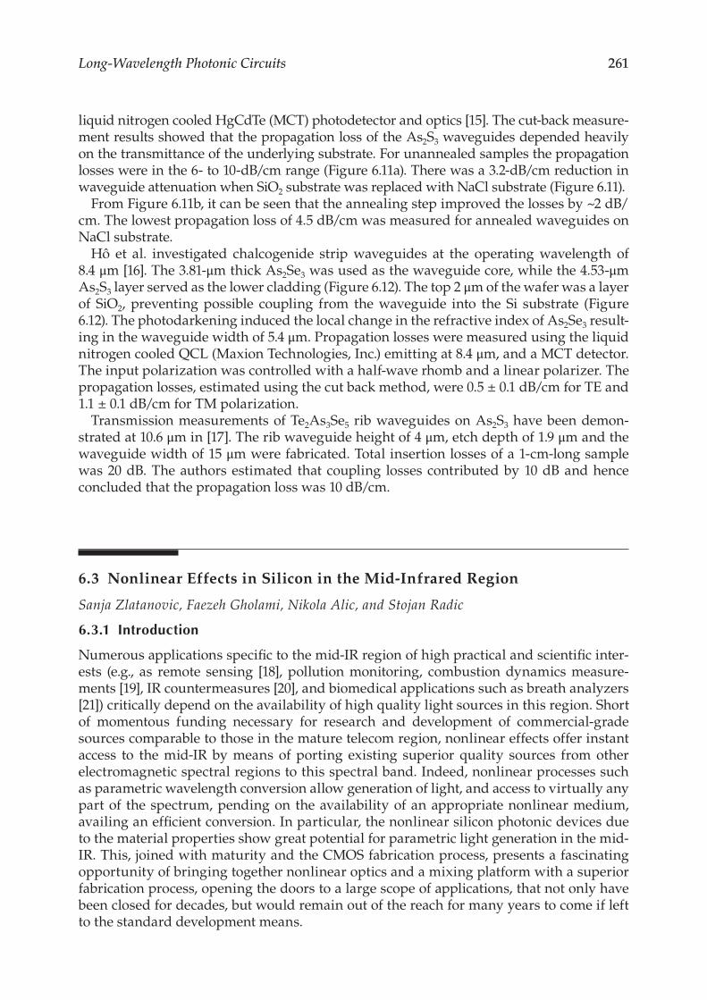
FIGURE 6.12Multilayer film and channel waveguide. (a) Schematic diagram of multilayer film channel waveguide after deposition and laser writing. (b) SEM cross-section image of the film, with thickness of each layer. (c) Optical microscope image of channel waveguide. (From N. Hô, M. C. Phillips, H. Qiao, P. J. Allen, K. Krishnaswami, B. J. Riley, T. L. Myers, and N. C. Anheier, Jr., Opt. Lett. vol. 31, 1860–1862, 2006.)
261Long-Wavelength Photonic Circuits
liquid nitrogen cooled HgCdTe (MCT) photodetector and optics [15]. The cut-back measure-ment results showed that the propagation loss of the As2S3 waveguides depended heavily on the transmittance of the underlying substrate. For unannealed samples the propagation losses were in the 6- to 10-dB/cm range (Figure 6.11a). There was a 3.2-dB/cm reduction in waveguide attenuation when SiO2 substrate was replaced with NaCl substrate (Figure 6.11).
From Figure 6.11b, it can be seen that the annealing step improved the losses by ~2 dB/cm. The lowest propagation loss of 4.5 dB/cm was measured for annealed waveguides on NaCl substrate.
Hô et al. investigated chalcogenide strip waveguides at the operating wavelength of 8.4 μm [16]. The 3.81-μm thick As2Se3 was used as the waveguide core, while the 4.53-μm As2S3 layer served as the lower cladding (Figure 6.12). The top 2 μm of the wafer was a layer of SiO2, preventing possible coupling from the waveguide into the Si substrate (Figure 6.12). The photodarkening induced the local change in the refractive index of As2Se3 result-ing in the waveguide width of 5.4 μm. Propagation losses were measured using the liquid nitrogen cooled QCL (Maxion Technologies, Inc.) emitting at 8.4 μm, and a MCT detector. The input polarization was controlled with a half-wave rhomb and a linear polarizer. The propagation losses, estimated using the cut back method, were 0.5 ± 0.1 dB/cm for TE and 1.1 ± 0.1 dB/cm for TM polarization.
Transmission measurements of Te2As3Se5 rib waveguides on As2S3 have been demon-strated at 10.6 μm in [17]. The rib waveguide height of 4 μm, etch depth of 1.9 μm and the waveguide width of 15 μm were fabricated. Total insertion losses of a 1-cm-long sample was 20 dB. The authors estimated that coupling losses contributed by 10 dB and hence concluded that the propagation loss was 10 dB/cm.
6.3 Nonlinear Effects in Silicon in the Mid-Infrared Region
Sanja Zlatanovic, Faezeh Gholami, Nikola Alic, and Stojan Radic
6.3.1 Introduction
Numerous applications specific to the mid-IR region of high practical and scientific inter-ests (e.g., as remote sensing [18], pollution monitoring, combustion dynamics measure-ments [19], IR countermeasures [20], and biomedical applications such as breath analyzers [21]) critically depend on the availability of high quality light sources in this region. Short of momentous funding necessary for research and development of commercial-grade sources comparable to those in the mature telecom region, nonlinear effects offer instant access to the mid-IR by means of porting existing superior quality sources from other electromagnetic spectral regions to this spectral band. Indeed, nonlinear processes such as parametric wavelength conversion allow generation of light, and access to virtually any part of the spectrum, pending on the availability of an appropriate nonlinear medium, availing an efficient conversion. In particular, the nonlinear silicon photonic devices due to the material properties show great potential for parametric light generation in the mid-IR. This, joined with maturity and the CMOS fabrication process, presents a fascinating opportunity of bringing together nonlinear optics and a mixing platform with a superior fabrication process, opening the doors to a large scope of applications, that not only have been closed for decades, but would remain out of the reach for many years to come if left to the standard development means.
262 Handbook of Silicon Photonics
Two material properties that make silicon suitable for nonlinear applications are its strong optical nonlinearity and large linear refractive index. Crystalline silicon possesses strong nonlinearity, nearly 200 times larger than that of silica, potentially allowing effi-cient nonlinear interactions in subcentimeter length devices. Moreover, due to the large linear refractive index of silicon (n = 3.47), optical modes can further be confined to the submicron scale cross sections in the silicon waveguides, providing yet another aspect for miniaturization as well as a nonlinear interaction enhancement. Silicon waveguides have previously been used in optical processing experiments in the near-IR. However, the applications on which this section focuses have been extended to the mid-IR spec-tral region. The main benefit from the operation in the mid-IR stems from the absence of parasitic nonlinear absorption that renders silicon performance in the near-IR part of the spectrum rather limited. Indeed, the performance of nonlinear silicon devices in the near-IR is greatly hindered by two-photon absorption (TPA) and the associated free-car-rier absorption (FCA). However, the deleterious TPA vanishes at the wavelengths beyond 2.25 μm, corresponding to photon energies lower than half of the material band-gap [22, 23]. Consequently, the operation of nonlinear silicon devices in the mid-IR does not suffer from this strong parasitic nonlinear absorption effect. While other multi-photon absorp-tion effects exist at the mid-IR wavelengths, their magnitude is much smaller and does not present a significant obstacle to the performance of silicon devices. It is primarily for this reason that the mid-IR potentially presents a superior region for operating silicon nonlinear devices, allowing them to unleash their full potential, unimpeded by the shorter wavelength operational obstacles.
The remainder of this section is organized as follows: we shall commence with a basic overview of optical nonlinearities and nonlinear material properties of silicon in the mid-IR region, as well as the associated anisotropy and dispersion. The main properties of the silicon waveguides contributing to efficient nonlinear interactions, supported with recent experimental results will be presented next. Finally we will conclude with experimental demonstrations of the main nonlinear phenomena, including Raman amplification [24], parametric amplification [25] and the four-wave mixing [26].
6.3.2 Nonlinear Optics in Silicon
Nonlinear optical phenomena fundamentally rely on interaction of high-intensity light beams with matter. In fact, the presence of a strong light beam can have a profound effect on the optical properties of select materials. Mathematically, this effect is described by the electric field-dependent polarizability, P, as [27]
P r E r E r E r E( , ) ( ( , ) : ( , ) ( , ) (( ) ( ) ( )t t t t= + +⋅ε χ χ χ01 2 3 � rr E r E r, ) ( , ) ( , ) )t t t +� , (6.1)
assuming instantaneous nonlinear response, where χ(n) is optical susceptibility tensor of the nth order. Silicon has a cubic crystalline structure of m3m class [27]. Being a centro-symmetric crystal, the second-order nonlinearity cannot exist in silicon [27], while the third-order nonlinearity is present. The third-order nonlinearity governs phenomena such as self-focusing in the spatial domain, and self-phase modulation, spontaneous, and stim-ulated Raman scattering, Brillouin scattering, Kerr effect, two-photon absorption (TPA), and four-wave mixing (FWM), as spatial domain temporal counterparts. The third-order susceptibility tensor of silicon contains twenty one nonzero elements, of which only four are independent due to the crystallographic structure [27]. These tensor components are namely χ1111
3( ), χ1122
3( ), χ1212
3( ), χ1221
3( ), where numerical subscripts 1, 2, and 3 are for x, y, and z
263Long-Wavelength Photonic Circuits
directions, respectively. Furthermore, assuming small dispersion of nonlinear susceptibil-ity and applying Kleinman symmetry [27] leads to only two independent tensor compo-nents χ1111
3( ), χ1122
3( ) [28].
The values of χ3 are typically derived from measured values of optical Kerr nonlinearity n2 and TPA coefficient βTPA. The relation between effective susceptibility, and these param-eters are given by
3 4 202 2 3
2ω ε χ ω β/ / /( ) ( )c n cn ieff TPA= + (6.2)
The third-order nonlinearity in silicon is anisotropic and is responsible for nonlinear processes, based on polarization of the input light. Both Kerr coefficient and TPA coeffi-cient exhibit anisotropy [29]. Furthermore, it has also been demonstrated that anisotropy in the Raman tensor plays a crucial role for Raman amplification [23, 30]. The magnitude of n2 and βTPA anisotropy has been measured by Zhang et al. [29]. In particular, this study has shown that both of these parameters decrease by about 12% from maximum when the direction of the polarization is changed. These results have been used to deduce anisot-ropy of χeff
( )3 itself in the region between 1.2 and 2.4 μm. It has been found that two indepen-dent components of the third-order susceptibility have the ratio of χ χ1111
311223 2 36( ) ( ) ~ ./ ,
constant over the entire measured wavelength range.
6.3.3 Two-Photon Absorption and Kerr Coefficient
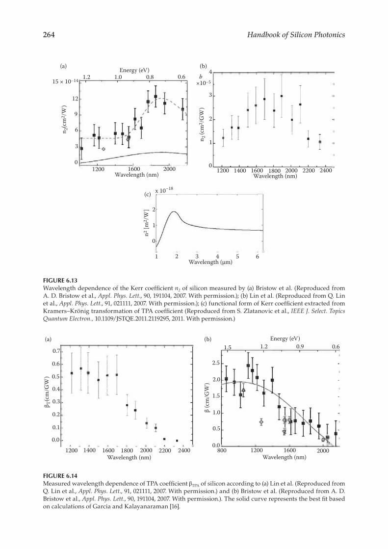
The measurements of absolute values of the Kerr and TPA coefficients for silicon were reported in the mid-IR region up to 2.35 μm [31, 32]. In the near and mid-IR region, the silicon third-order nonlinearity exhibits significant dispersion due to the photon energies close to the half of the band-gap. The data presented in Figure 6.13a,b demonstrate that the order of magnitude (1 × 10–18 m2/W) of the Kerr coefficient is consistent across the lit-erature. The functional forms of the Kerr coefficient dispersion also agree very well. The Kerr coefficient exhibits a peak between 1800 and 1900 nm, and subsequently decreases at longer wavelengths. An estimate of the Kerr coefficient values beyond 2.35 μm is obtained by Kramers–Krönig transform of TPA data (Figure 6.13c). Kramers–Krönig transform accurately predicts the functional form of the Kerr coefficient dispersion; however, it does underestimate the magnitude of the Kerr coefficient. This discrepancy is likely due to the neglect of Raman and quadratic Stark effect contributions. The calculated Kerr coefficient dispersion curve (Figure 6.13c) shows that a slower decrease in magnitude of the Kerr coef-ficient is expected at longer wavelengths, wheareas the trend is maintained even deeper into the mid-IR. It is this finding that so favorably promotes silicon as a mid-IR mixing platform. Furthermore, these implications are further supported by the measured silicon nonlinearity of n2 of 1.9 × 10⁻¹⁸ m2/W at 10 μm [33].
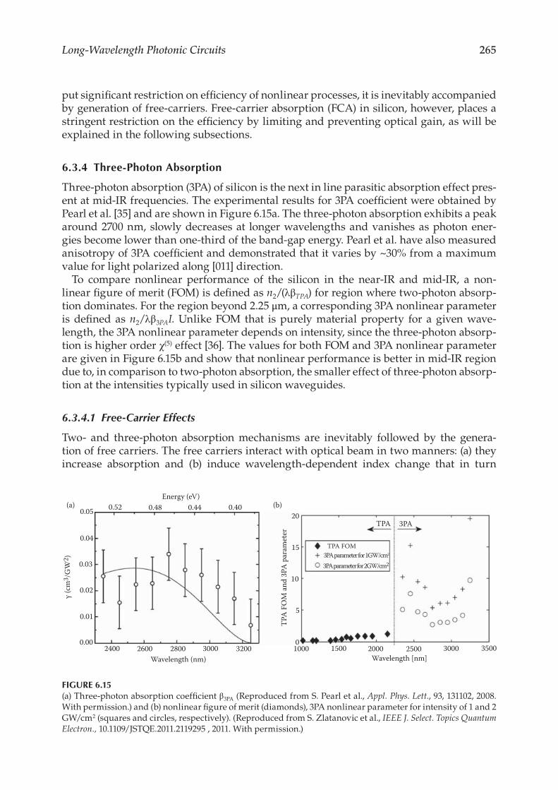
In contrast, and as shown in Figure 6.14a,b, the two-photon absorption is strong at near-IR frequencies and limits the efficiency of nonlinear effects. The functional form of TPA dis-persion obtained using theory developed by Garcia and Kalayanaraman [34], taking into account three types of indirect transitions that contribute to TPA (forbidden–forbidden, allowed–forbidden, and allowed–allowed) is in a very good agreement with the measured data. The TPA coefficient has a broad peak around 1.1 μm (corresponding to the energy of the indirect band-gap) and decreases steadily for longer wavelengths. It completely van-ishes at wavelengths beyond 2.25 μm. This is of crucial importance for efficient operation of nonlinear silicon devices at longer mid-IR wavelengths. While the TPA itself does not
264 Handbook of Silicon Photonics
(a) Energy (eV)1.2 1.0 0.8 0.6
15 × 10−14
12
9
6
3
0
n 2(c
m2 /
W)
1200 1600 2000Wavelength (nm)
4
×10−5b
3
2
1
01200 1400 1600 1800 2000 2200 2400
Wavelength (nm)
n 2 (c
m2 /
GW
)
(b)
2
1
x 10−18
0
1 2 3 4 5 6Wavelength (μm)
n2 [m
2 /W
]
(c)
FIGURE 6.13Wavelength dependence of the Kerr coefficient n2 of silicon measured by (a) Bristow et al. (Reproduced from A. D. Bristow et al., Appl. Phys. Lett., 90, 191104, 2007. With permission.); (b) Lin et al. (Reproduced from Q. Lin et al., Appl. Phys. Lett., 91, 021111, 2007. With permission.); (c) functional form of Kerr coefficient extracted from Kramers–Krönig transformation of TPA coefficient (Reproduced from S. Zlatanovic et al., IEEE J. Select. Topics Quantum Electron., 10.1109/JSTQE.2011.2119295, 2011. With permission.)
0.7
0.6
0.5
0.4
0.3
0.2
0.1
0.0
(a) (b)
1200 1400 1600 1800 2000 2200 2400Wavelength (nm)
β T(c
m/G
W)
β (c
m/G
W)
2.5
2.0
1.5
1.0
0.5
0.0800 1200 1600 2000
Wavelength (nm)
1.5 1.2 0.9 0.6Energy (eV)
FIGURE 6.14Measured wavelength dependence of TPA coefficient βTPA of silicon according to (a) Lin et al. (Reproduced from Q. Lin et al., Appl. Phys. Lett., 91, 021111, 2007. With permission.) and (b) Bristow et al. (Reproduced from A. D. Bristow et al., Appl. Phys. Lett., 90, 191104, 2007. With permission.). The solid curve represents the best fit based on calculations of Garcia and Kalayanaraman [16].
265Long-Wavelength Photonic Circuits
put significant restriction on efficiency of nonlinear processes, it is inevitably accompanied by generation of free-carriers. Free-carrier absorption (FCA) in silicon, however, places a stringent restriction on the efficiency by limiting and preventing optical gain, as will be explained in the following subsections.
6.3.4 Three-Photon Absorption
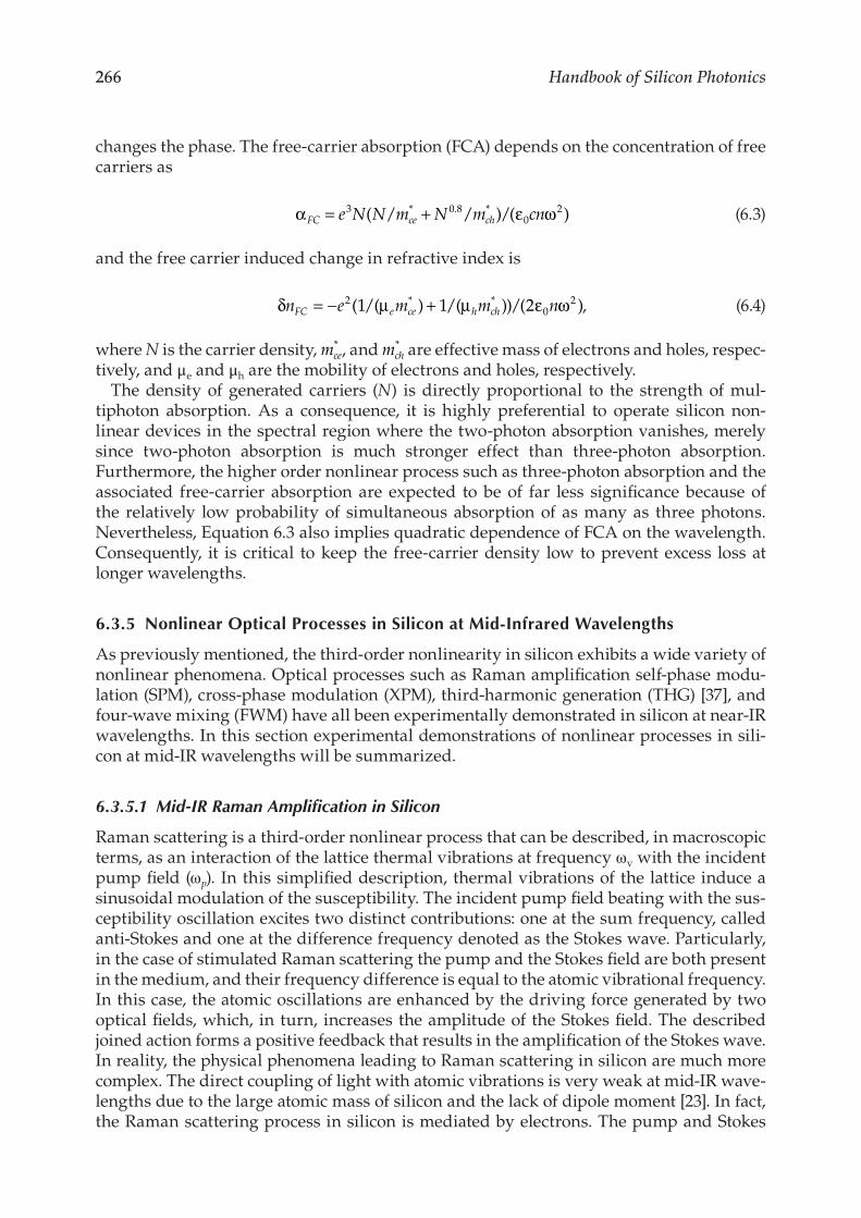
Three-photon absorption (3PA) of silicon is the next in line parasitic absorption effect pres-ent at mid-IR frequencies. The experimental results for 3PA coefficient were obtained by Pearl et al. [35] and are shown in Figure 6.15a. The three-photon absorption exhibits a peak around 2700 nm, slowly decreases at longer wavelengths and vanishes as photon ener-gies become lower than one-third of the band-gap energy. Pearl et al. have also measured anisotropy of 3PA coefficient and demonstrated that it varies by ~30% from a maximum value for light polarized along [011] direction.
To compare nonlinear performance of the silicon in the near-IR and mid-IR, a non-linear figure of merit (FOM) is defined as n2/(λβTPA) for region where two-photon absorp-tion dominates. For the region beyond 2.25 μm, a corresponding 3PA nonlinear parameter is defined as n2/λβ3PAI. Unlike FOM that is purely material property for a given wave-length, the 3PA nonlinear parameter depends on intensity, since the three-photon absorp-tion is higher order χ(5) effect [36]. The values for both FOM and 3PA nonlinear parameter are given in Figure 6.15b and show that nonlinear performance is better in mid-IR region due to, in comparison to two-photon absorption, the smaller effect of three-photon absorp-tion at the intensities typically used in silicon waveguides.
6.3.4.1 Free-Carrier Effects
Two- and three-photon absorption mechanisms are inevitably followed by the genera-tion of free carriers. The free carriers interact with optical beam in two manners: (a) they increase absorption and (b) induce wavelength-dependent index change that in turn
(b)(a)0.05 0.52 0.48 0.44 0.40
Energy (eV)
20
15
10
5
01000 1500 2000 2500 3000 3500
Wavelength [nm]
TPA 3PA
TPA FOM3PA parameter for 1GW/cm2
3PA parameter for 2GW/cm2
0.04
0.03
0.02
0.01
0.002400 2600 2800 3000 3200
Wavelength (nm)
γ (c
m3 /
GW
2 )
TPA
FO
M a
nd 3
PA p
aram
eter
FIGURE 6.15(a) Three-photon absorption coefficient β3PA (Reproduced from S. Pearl et al., Appl. Phys. Lett., 93, 131102, 2008. With permission.) and (b) nonlinear figure of merit (diamonds), 3PA nonlinear parameter for intensity of 1 and 2 GW/cm2 (squares and circles, respectively). (Reproduced from S. Zlatanovic et al., IEEE J. Select. Topics Quantum Electron., 10.1109/JSTQE.2011.2119295 , 2011. With permission.)
266 Handbook of Silicon Photonics
changes the phase. The free-carrier absorption (FCA) depends on the concentration of free carriers as
α ε ωFC ce che N N m N m cn= +3 0 80
2( ) ( )* . */ / / (6.3)
and the free carrier induced change in refractive index is
δ μ μ ε ωn e m m nFC e ce h ch= − +20
21 1 2( ) )) ( )* */( /( / , (6.4)
where N is the carrier density, mce* , and mch
* are effective mass of electrons and holes, respec-tively, and μe and μh are the mobility of electrons and holes, respectively.
The density of generated carriers (N) is directly proportional to the strength of mul-tiphoton absorption. As a consequence, it is highly preferential to operate silicon non-linear devices in the spectral region where the two-photon absorption vanishes, merely since two-photon absorption is much stronger effect than three-photon absorption. Furthermore, the higher order nonlinear process such as three-photon absorption and the associated free-carrier absorption are expected to be of far less significance because of the relatively low probability of simultaneous absorption of as many as three photons. Nevertheless, Equation 6.3 also implies quadratic dependence of FCA on the wavelength. Consequently, it is critical to keep the free-carrier density low to prevent excess loss at longer wavelengths.
6.3.5 Nonlinear Optical Processes in Silicon at Mid-Infrared Wavelengths
As previously mentioned, the third-order nonlinearity in silicon exhibits a wide variety of nonlinear phenomena. Optical processes such as Raman amplification self-phase modu-lation (SPM), cross-phase modulation (XPM), third-harmonic generation (THG) [37], and four-wave mixing (FWM) have all been experimentally demonstrated in silicon at near-IR wavelengths. In this section experimental demonstrations of nonlinear processes in sili-con at mid-IR wavelengths will be summarized.
6.3.5.1 Mid-IR Raman Amplification in Silicon
Raman scattering is a third-order nonlinear process that can be described, in macroscopic terms, as an interaction of the lattice thermal vibrations at frequency ωv with the incident pump field (ωp). In this simplified description, thermal vibrations of the lattice induce a sinusoidal modulation of the susceptibility. The incident pump field beating with the sus-ceptibility oscillation excites two distinct contributions: one at the sum frequency, called anti-Stokes and one at the difference frequency denoted as the Stokes wave. Particularly, in the case of stimulated Raman scattering the pump and the Stokes field are both present in the medium, and their frequency difference is equal to the atomic vibrational frequency. In this case, the atomic oscillations are enhanced by the driving force generated by two optical fields, which, in turn, increases the amplitude of the Stokes field. The described joined action forms a positive feedback that results in the amplification of the Stokes wave. In reality, the physical phenomena leading to Raman scattering in silicon are much more complex. The direct coupling of light with atomic vibrations is very weak at mid-IR wave-lengths due to the large atomic mass of silicon and the lack of dipole moment [23]. In fact, the Raman scattering process in silicon is mediated by electrons. The pump and Stokes
267Long-Wavelength Photonic Circuits
wave separation in silicon is ~15.6 THz and the stimulated Raman scattering gain has a rel-atively narrow bandwidth of 105 GHz. The stimulated Raman process can be described by
dIs/dz = gRIpIs, (6.5)
where gR is the Raman gain coefficient that is obtained from the so called Raman suscep-tibility using g n nR ijkl s s p= 6 0
3π μ χ λ( ) ( )/ . The value of the Raman gain coefficient at 1550 nm is in the range of 10–20 cm/GW [38, 39] and scales inversely with wavelength as 1/λs, leading to diminished levels at mid-IR wavelengths.
The experimental demonstration of Raman amplification in mid-IR has been reported by Raghunathan et al. [24]. In this experiment, a signal at 3.39 μm was amplified using a pump at 2.88 μm. The active medium was a 2.5-cm-long [100] silicon crystal. The Raman on–off gain obtained in this experiment was ~12 dB as shown in Figure 6.16. The satura-tion of Raman gain at higher pump intensities was due to damage of the sample surface.
For the measured gain in this experiment, the value of Raman gain coefficient falls in the range between 4.5 and 9 cm/GW that is predicted from the measurements at 1550 nm and the 1/λs dependence.
This experiment was the first successful demonstration of Raman gain in silicon at mid-IR wavelengths. In more recent attempts, the stimulated Raman scattering at mid-IR wavelengths was applied for beam cleanup [40]. In this experiment an amplified near-diffraction-limited Stokes beam was obtained using a severely aberrated pump.
6.3.5.2 Self-Phase Modulation at Mid-IR Wavelengths
Self-phase modulation (SPM) is a process in which refractive index change is induced by the mere presence of the pump. Owing to the refractive index dependence on the inten-sity, a strong pulsed pump induces a temporal phase shift, thus causing a frequency shift (or, equivalently photon generation at the immediately adjacent frequencies—in a continu-ous manner). As a consequence, the pulse spectrum broadens and develops a characteristic multiple-peak structure. The SPM was investigated in silicon waveguides at the mid-IR [41].
14
12
10
8
6
4
2
00 100 200 300
Stok
es o
n–off
gai
n (d
b)
Pump intensity (MW/cm2)
FIGURE 6.16Raman on–off gain as a function of effective pump intensity interacting with Stokes input. (Reproduced from V. Raghunathan et al., Opt. Express, 15, 14355–14362, 2007. With permission.)
268 Handbook of Silicon Photonics
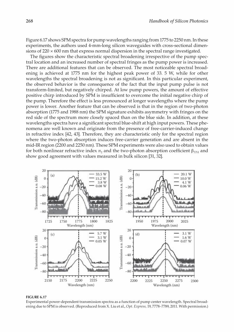
Figure 6.17 shows SPM spectra for pump wavelengths ranging from 1775 to 2250 nm. In these experiments, the authors used 4-mm-long silicon waveguides with cross-sectional dimen-sions of 220 × 600 nm that express normal dispersion in the spectral range investigated.
The figures show the characteristic spectral broadening irrespective of the pump spec-tral location and an increased number of spectral fringes as the pump power is increased. There are additional features that can be observed. The most noticeable spectral broad-ening is achieved at 1775 nm for the highest peak power of 33. 5 W, while for other wavelengths the spectral broadening is not as significant. In this particular experiment, the observed behavior is the consequence of the fact that the input pump pulse is not transform- limited, but negatively chirped. At low pump powers, the amount of effective positive chirp introduced by SPM is insufficient to overcome the initial negative chirp of the pump. Therefore the effect is less pronounced at longer wavelengths where the pump power is lower. Another feature that can be observed is that in the region of two-photon absorption (1775 and 1988 nm) the SPM signature exhibits asymmetry with fringes on the red side of the spectrum more closely spaced than on the blue side. In addition, at these wavelengths spectra have a significant spectral blue-shift at high input powers. These phe-nomena are well known and originate from the presence of free-carrier-induced change in refractive index [42, 43]. Therefore, they are characteristic only for the spectral region where the two-photon absorption induces free-carrier generation and are absent in the mid-IR region (2200 and 2250 nm). These SPM experiments were also used to obtain values for both nonlinear refractive index n2 and the two-photon absorption coefficient βTPA and show good agreement with values measured in bulk silicon [31, 32].
2150 2175 2200 2225 2250
Wavelength (nm)
Wavelength (nm) Wavelength (nm)
Wavelength (nm)
Tran
smiss
ion
a.u.
(dB)
20
0
–20
–40
–60
–80
Tran
smiss
ion
a.u.
(dB)
20
0
–20
–40
–60
–80
Tran
smiss
ion
a.u.
(dB)
20
0
–20
–40
–60
–80
Tran
smiss
ion
a.u.
(dB)
20
0
–20
–40
–60
–80
2200 2225 2250 2275 2300
3.1 W1.6 W
0.07 W
(d)
(b)(a)
(c)
1950 1975 2000 2025
20.1 W10.0 W
4.1 W0.06 W
33.5 W15.2 W
3.8 W0.08 W
5.7 W3.1 W
0.05 W
1725 1750 1775 1800 1825
FIGURE 6.17Experimental power-dependent transmission spectra as a function of pump center wavelength. Spectral broad-ening due to SPM is observed. (Reproduced from X. Liu et al., Opt. Express, 19, 7778–7789, 2011. With permission.)
269Long-Wavelength Photonic Circuits
6.3.5.3 Four-Wave Mixing and Parametric Amplification in the Mid-IR
Four-wave mixing (FWM) is a nonlinear process in which three photons (not necessarily all distinct) interact, whereby a fourth photon satisfying the overall energy conservation is generated, as a consequence. In particular in what is generally denoted to as a single pump (degenerate) four-wave mixing configuration, two pump photons are annihilated to generate two photons one at signal and one at idler frequency. The physics of the process can simply be described in terms of energy and momentum conservation (phase-matching condition) in the nondegenerate pump case as:
ωi = ωp1 + ωp2 − ωs (6.6)
Δk = 2γP0 – ΔkL = 2γP0–(kp1 + kp2 − ks − ki), (6.7)
where ωi, ωs, ωp1, ωp2 are idler, signal, and pumps frequencies and ks, ki, kp1, kp2 are wave vectors defined as k = neff ω/c, where neff is the effective refractive index, γ is effective non-linearity and P0 is pump power. In a simplified form, the effective nonlinearity can be expressed as γ = n2ω/(c Aeff), where Aeff is effective modal area. Efficient FWM requires phase matching, which can be achieved through waveguide dispersion engineering. Due to the strong optical confinement of the optical mode in silicon waveguides, the dispersion is dominated by waveguide geometry. By changing the dimensions of the waveguide, the dispersion properties can be modified to satisfy the requirements of a particular conver-sion process. To fulfill the phase-matching condition (the momentum conservation rela-tionship), Δk must be equal to zero. The conversion efficiency defined as a ratio of the idler output to signal input power can be expressed in a simplified manner as [44]
η(P0) = (γP0/g)2 × sinh2(gL), (6.8)
where
g = (γP0ΔkL − (ΔkL/2)2)1/2. (6.9)
The conversion bandwidth strongly depends on the waveguide dispersion. In addi-tion, due to very large values of n2 in silicon waveguides, conversion is possible in the centimeter- scale lengths, which translates into higher conversion bandwidth. As pointed out previously, the effective nonlinearity of silicon waveguides depends inversely on the effective modal area and wavelength. This property, thus, implies nonlinearity decreases at longer wavelengths due to the increased mode size.
The potential of four-wave mixing in silicon in the mid-IR was recognized by Painter et al. [45]. They theoretically analyzed parametric mixing in silicon waveguides and micro-resonators. In addition, an extensive theoretical analysis of the dispersion in the mid-IR for the silicon waveguides on platforms such as silicon-on-sapphire, silicon on SiO2, and silicon with air cladding was published by Tien et al. [46]. Recently, several experiments reported four-wave mixing in silicon waveguides in the mid-IR spectral range where non-linear absorption is not detrimental to the waveguide performance.
Wavelength conversion to mid-IR was demonstrated in 3.8-mm-long silicon wave-guides on SOI platform using an ultra-compact telecom-derived pump source at 2025 nm [26, 47]. Operation at this wavelength is characterized by low TPA. The silicon waveguides had cross-sectional dimensions of 1060 × 250 nm. FWM was performed with long pump
270 Handbook of Silicon Photonics
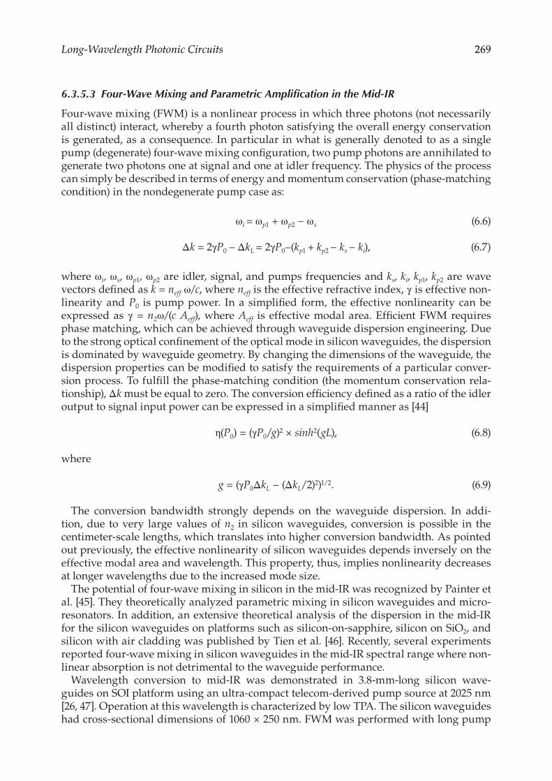
pulses of 1ns-duration which was comparable with the free-carrier lifetime in silicon and can therefore be considered a quasi-CW operation. With the pump power of 176 mW, the conversion efficiency of −22.5 dB was achieved across 240 nm bandwidth (Figure 6.18, left).
Furthermore, light was generated at the mid-IR wavelengths up to 2388 nm (Figure 6.18, right). The reported measured nonlinearity in the waveguides was 97.3(Wm)−1 and agrees well with measurements of n2 reported by Bristow et al. [31].
A broadband parametric conversion to the mid-IR has also been demonstrated using the continuous wave (CW) pumps [48, 49]. In the demonstration, using pump at 1950 nm a continuously tunable wavelength conversion was observed across 324 nm and the idler was generated at the wavelength of 2384 nm.
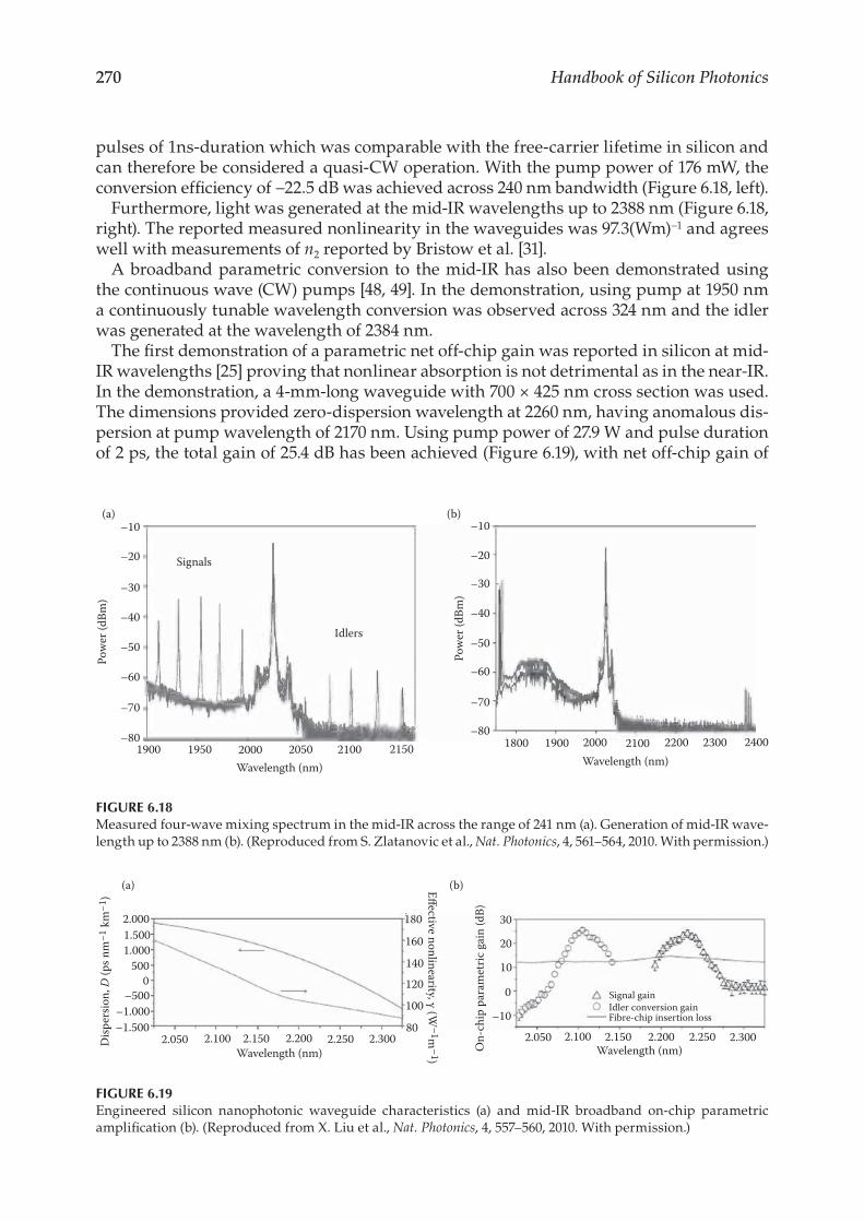
The first demonstration of a parametric net off-chip gain was reported in silicon at mid-IR wavelengths [25] proving that nonlinear absorption is not detrimental as in the near-IR. In the demonstration, a 4-mm-long waveguide with 700 × 425 nm cross section was used. The dimensions provided zero-dispersion wavelength at 2260 nm, having anomalous dis-persion at pump wavelength of 2170 nm. Using pump power of 27.9 W and pulse duration of 2 ps, the total gain of 25.4 dB has been achieved (Figure 6.19), with net off-chip gain of
–10
–20
–30
–40
–60
–70
–80
–50
–10
–20
–30
–40
–60
–70
–80
–50
1900 1950 2000 2050 2100 2150 1800 1900 2000 2100 2200 2300 2400
Wavelength (nm) Wavelength (nm)
Pow
er (d
Bm)
Pow
er (d
Bm)
Signals
Idlers
(a) (b)
FIGURE 6.18Measured four-wave mixing spectrum in the mid-IR across the range of 241 nm (a). Generation of mid-IR wave-length up to 2388 nm (b). (Reproduced from S. Zlatanovic et al., Nat. Photonics, 4, 561–564, 2010. With permission.)
2.0001.5001.000
5000
–500–1.000–1.500
2.050 2.100 2.150 2.200 2.250 2.300
180
160
140
120
100
80
Wavelength (nm) Wavelength (nm)Disp
ersio
n, D
(ps n
m−1
km
−1)
30
20
10
0
–10
2.050 2.100 2.150 2.200 2.250 2.300
Signal gainIdler conversion gainFibre-chip insertion loss
On-
chip
par
amet
ric g
ain
(dB)
Effective nonlinearity, γ (W–1m
–1)
(a) (b)
FIGURE 6.19Engineered silicon nanophotonic waveguide characteristics (a) and mid-IR broadband on-chip parametric amplification (b). (Reproduced from X. Liu et al., Nat. Photonics, 4, 557–560, 2010. With permission.)
271Long-Wavelength Photonic Circuits
10 dB for the signal and 13 dB for the idler. The overall on-chip gain bandwidth spanned from 2060 to 2280 nm. This experiment was the first demonstration of a broadband net off-chip gain in silicon.
6.3.6 Conclusion
Silicon waveguides present a promising nonlinear platform for the mid-IR region in par-ticular due to the inherent high nonlinearity and the negligible effect of nonlinear absorp-tion in this part of the spectrum. Consequently, detrimental effects typical for the near-IR region, such as two-photon absorption and associated free-carrier absorption are alto-gether avoided by pumping silicon at mid-IR wavelengths. As discussed, operation at the mid-IR enabled the first net off-chip gain in silicon, which, in itself, represented a mile-stone of significant importance for the technology.
In summary, this, by no means all-encompassing, review of nonlinear properties of silicon as a nonlinear platform shows its extraordinary potential to provide access to the entire mid-IR region with sufficient conversion efficiency. More importantly, the results obtained so far single out the silicon waveguide platform as a strong contender for a vast range of applications, pertinent to this region and overviewed in this chapter.
6.4 Long Wavelength Silicon-Based Sources and Detectors
Zoran Ikonic and Robert W. Kelsall
6.4.1 Introduction
Sources and detectors are essential elements of any photonic circuit, and considerable effort has been devoted to the development of lasers and photodetectors, which either use silicon as an active material or are compatible with silicon processing. In the long wave-length range, there has been a 20-year history of detector research, resulting in devices that, although outperformed by their III/V-based counterparts as stand-alone compo-nents, can be readily implemented in a Si-based environment. Development of Si-based long wavelength lasers, which has been ongoing for at least 10 years, has proved to be a far more difficult task, particularly for operation at practical operating temperatures. This sec-tion describes different approaches to source and detector design, and the results achieved so far in these areas.
6.4.2 Quantum Cascade Lasers
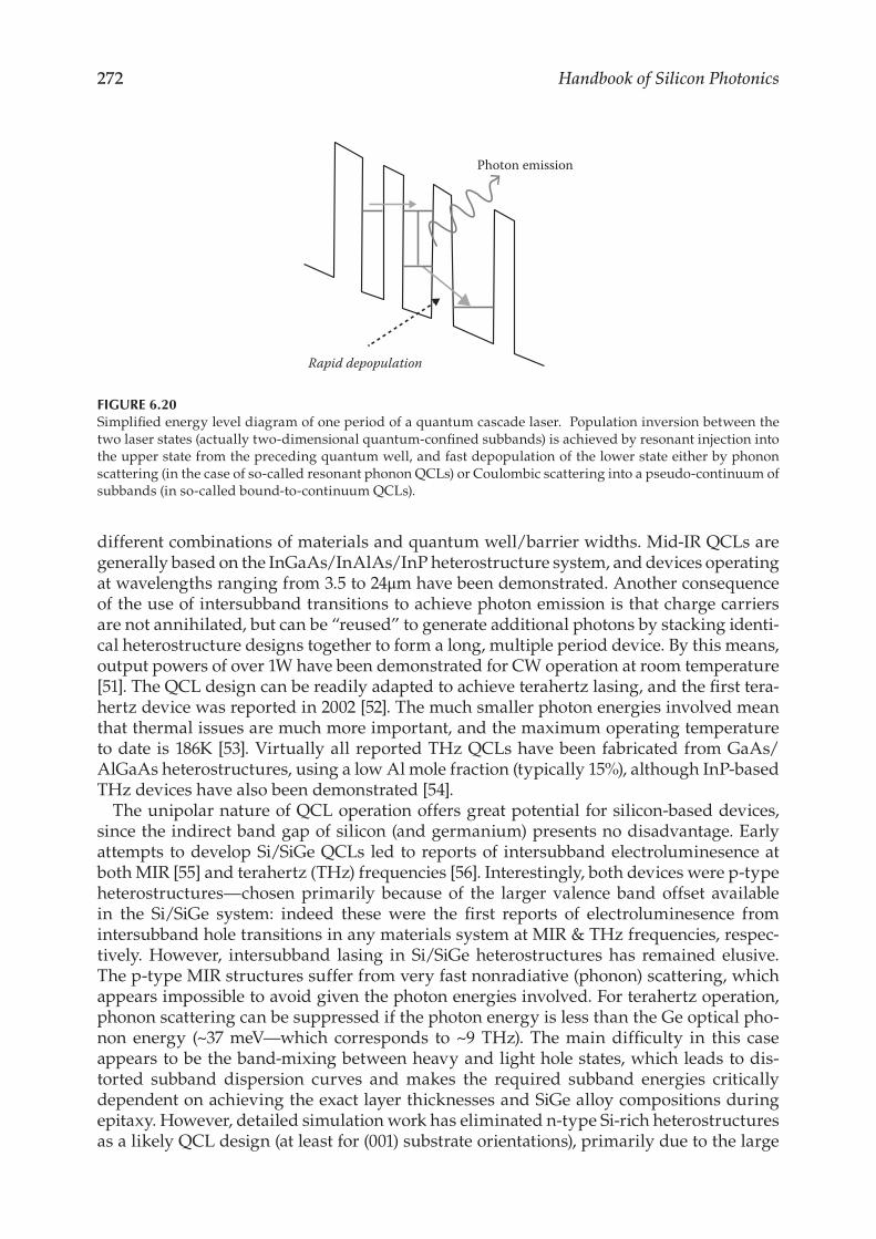
Early mid-IR (MIR) lasers were based on narrow band-gap semiconductors, such as the IV–VI lead salt materials, and generally required cooling to suppress Auger recombination. The advent of the quantum cascade laser (QCL) in 1994 [50] led to a great improvement in mid-infrared source provision, providing coverage across much of the 3- to 5-μm and 8- to 14-μm atmospheric windows. In contrast to conventional semiconductor lasers, QCLs are unipolar devices, emitting photons via transitions between quantum confined subbands in a multiple quantum well heterostructure, rather than via interband recombination (see Figure 6.20). Consequently, a wide range of laser wavelengths can be achieved using
272 Handbook of Silicon Photonics
different combinations of materials and quantum well/barrier widths. Mid-IR QCLs are generally based on the InGaAs/InAlAs/InP heterostructure system, and devices operating at wavelengths ranging from 3.5 to 24μm have been demonstrated. Another consequence of the use of intersubband transitions to achieve photon emission is that charge carriers are not annihilated, but can be “reused” to generate additional photons by stacking identi-cal heterostructure designs together to form a long, multiple period device. By this means, output powers of over 1W have been demonstrated for CW operation at room temperature [51]. The QCL design can be readily adapted to achieve terahertz lasing, and the first tera-hertz device was reported in 2002 [52]. The much smaller photon energies involved mean that thermal issues are much more important, and the maximum operating temperature to date is 186K [53]. Virtually all reported THz QCLs have been fabricated from GaAs/AlGaAs heterostructures, using a low Al mole fraction (typically 15%), although InP-based THz devices have also been demonstrated [54].
The unipolar nature of QCL operation offers great potential for silicon-based devices, since the indirect band gap of silicon (and germanium) presents no disadvantage. Early attempts to develop Si/SiGe QCLs led to reports of intersubband electroluminesence at both MIR [55] and terahertz (THz) frequencies [56]. Interestingly, both devices were p-type heterostructures—chosen primarily because of the larger valence band offset available in the Si/SiGe system: indeed these were the first reports of electroluminesence from intersubband hole transitions in any materials system at MIR & THz frequencies, respec-tively. However, intersubband lasing in Si/SiGe heterostructures has remained elusive. The p-type MIR structures suffer from very fast nonradiative (phonon) scattering, which appears impossible to avoid given the photon energies involved. For terahertz operation, phonon scattering can be suppressed if the photon energy is less than the Ge optical pho-non energy (~37 meV—which corresponds to ~9 THz). The main difficulty in this case appears to be the band-mixing between heavy and light hole states, which leads to dis-torted subband dispersion curves and makes the required subband energies critically dependent on achieving the exact layer thicknesses and SiGe alloy compositions during epitaxy. However, detailed simulation work has eliminated n-type Si-rich heterostructures as a likely QCL design (at least for (001) substrate orientations), primarily due to the large
Photon emission
Rapid depopulation
FIGURE 6.20Simplified energy level diagram of one period of a quantum cascade laser. Population inversion between the two laser states (actually two-dimensional quantum-confined subbands) is achieved by resonant injection into the upper state from the preceding quantum well, and fast depopulation of the lower state either by phonon scattering (in the case of so-called resonant phonon QCLs) or Coulombic scattering into a pseudo-continuum of subbands (in so-called bound-to-continuum QCLs).
273Long-Wavelength Photonic Circuits
effective mass of the silicon Δ valleys—which leads to very low intersubband material gains—and strong nonradiative scattering from the lowest Δ2 subbands into strain-split Δ4 valleys, which are closely located in energy [57]. n-type Si/SiGe structures grown on (111) substrates offer better prospects [58], but the most promising Si-based system appears to comprise Ge quantum wells and Ge-rich SiGe barriers with selective n-type doping. Recent developments in Ge-on-Si epitaxy (e.g., [59]) mean that such structures can be grown on relaxed Ge buffers on Si substrates.
For terahertz operation, the large size of the optical mode raises issues over laser cavity design. Conventional guided mode cavities would be so thick as to require impractically long epitaxial growth times. The approach developed for III–V terahertz QCLs has been, instead, to support surface plasmon modes pinned at the top and bottom of the cavity either by two metal layers (which requires wafer bonding) (so-called double metal waveguides) [60], or by a top metal layer and a doped semiconductor layer under the active region of the device (so-called single plasmon waveguides) [52]. Even so, terahertz QCL waveguide cavi-ties are typically 10 μm thick, which requires epitaxial growth of approximately 2000 lay-ers. This cannot be achieved by solid source Si/Ge MBE, because of the very slow growth times involved, but appears feasible via chemical vapor deposition (CVD), and possibly by gas-source molecular beam epitaxy (MBE). To date, growth of 4200 layers has been dem-onstrated by CVD (using a plasma enhanced approach) [61] and 1200 layers by gas source MBE [62]. These very thick quantum well stacks are well beyond the critical thickness limit for strain relaxation in a lattice-mismatched heterostructure. Therefore, strain-balanced designs must be used, in which well and barrier layers experience opposing lattice mis-match strains (compressive and tensile, respectively), and the whole structure is grown on a relaxed buffer whose alloy composition achieves net strain balance within each QCL period and therefore throughout the stack.
Unfortunately, doped silicon (and germanium) layers are much less effective than doped GaAs in pinning surface plasmon modes (at least for practically achievable doping densi-ties during epitaxy), so single plasmon waveguides of the form shown in reference [52] do not appear to be realizable in Ge/SiGe structures [63], although the use of surface grat-ings to support so-called “spoof” surface plasmon modes offers potential for achieving reasonable mode confinement (up to 40%) with low waveguide losses [64]. Double metal waveguides are more lossy than the single plasmon structures, due to strong free car-rier absorption in the metal layers, but provide almost complete mode confinement. Calculations show that a 10-μm Ge/SiGe QCL double metal cavity structure would have acceptable losses (~37 cm−1)—considerably less than the gain in appropriately designed cascade structures at low temperatures, and even offering potential for room temperature lasing [57]. The anticipated improvement in thermal performance, compared with III–V terahertz QCLs, stems from the lack of fast polar optical phonon scattering in Ge and Si (which competes with the lasing transition), and the higher thermal conductivity of the silicon substrate.
6.4.3 Intracenter-Based Terahertz Lasers
An alternative route to terahertz lasing in silicon—but also based on a unipolar device—is stimulated emission from transitions between impurity states in a bulk-doped structure. Within the simple, isotropic single-valley effective mass picture, the electronic structure of group V impurities (donors) in Si is hydrogen-like, with various transition energies falling in the THz range, and is sixfold degenerate due to the presence of six equivalent X-valleys in the conduction band. The deviation of the microscopic atomic potential in the
274 Handbook of Silicon Photonics
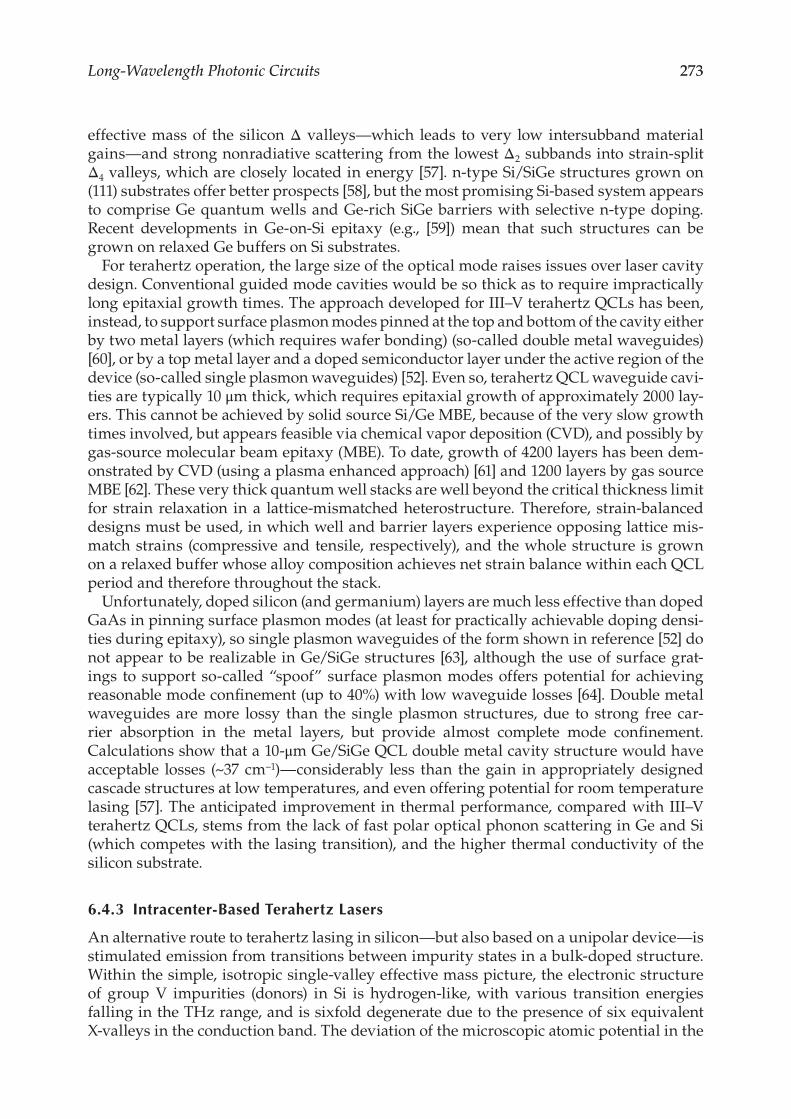
lattice from spherical symmetry (valley-orbit interaction) modifies the electronic structure, so that the 1s state splits into the lowest, ground state 1s(A), and higher 1s(E), and 1s(T2) states, above which come higher excited states 2p0, 2s, 2p±, etc., as shown in Figure 6.21. Stimulated emission in the THz range, first reported in [65], has been obtained on differ-ent transitions between donor states in silicon (“intracenter” transitions), using Si:P, Si:As, Si:Sb, and Si:Bi materials. A comprehensive review of these lasers is given in [66].
They operate only at very low temperatures, at which the impurities are not ionized. Optical pumping is performed by irradiating the doped Si by another (CO2) laser or by frequency tunable free-electron laser. In the former case, known as photoexcitation, an electron is excited from the ground, impurity-bound 1s(A) state high into the conduction band, from where it relaxes, by a cascade of optical and acoustic phonon emission events, toward the bottom of the conduction band, and eventually gets captured by the impurity, into its excited bound states, some of which acts as the upper laser state. In the latter case, known as intracenter optical pumping, an electron is excited from the ground directly into a designated excited bound impurity state. The detailed mechanism of laser action varies from one impurity type to another. The mechanism of population inversion in Si:P (and also Si:Sb) is the carrier accumulation in a long-lived bound 2p0 excited state, acting as the upper laser state, while the lower laser states 1s(E,T2) are almost empty, because the lifetime of 2p0 is ~10−9 s, larger by up to two orders of magnitude than that of 1s(E,T2), which makes Si:P and Si:Sb typical four-level laser systems. Lasing in Si:As and Si:Bi has also been achieved, the mechanism therein being somewhat different, due to resonant electron-phonon interaction which makes the 2s and 2p0 states also short-lived. The lasing transitions in these cases are 2p±–1s(T2,E), or from higher excited states into 2s or 2p0.
The emission frequency of these lasers depends on the type of donors and the operat-ing transition, and is in the 3.6- to 7-THz range, with a couple of longer-wavelength lines around 1.3–1.8 THz. There is a possibility of frequency tuning by applying stress. Uniaxial stress lowers the crystal symmetry and shifts and/or splits various levels of donor atoms, depending on the level character and stress orientation. In Si:P and Si:Sb lasers no tuning is possible because both the upper and lower laser state shift in the same way (however, the lasing threshold may be reduced by an order of magnitude [67]), while Si:Bi 2p±–1s(T2) laser transition can be stress-tuned by 3%/kbar [66]. Values of gain amount to ~0.5 cm−1
Si:P Si:Sb
conductionband
conductionband
10 m
eV
10 m
eV
CO2laser
pumping
CO2laser
pumping
1s(E) 1s(T2:Γ8)1s(T2:Γ8)
1s(E)1s(T2)
1s(A1) 1s(A1)
2p0 2p0
FIGURE 6.21Energy levels and lasing scheme in Si:P and Si:Sb laser [17]. Copyright IOP Ltd. Reproduced with permission.
275Long-Wavelength Photonic Circuits
for photoexcitation, and 5–10 cm−1 for the intracenter pumping scheme [68]. For a number of reasons (to prevent thermal ionization of long-lived states, keep the electron capture probability to acceptable values [69], preserve favorable ratio of relaxation rates of relevant states, etc.) the impurity based lasers operate only at low temperatures, e.g., up to 17 K for Si:P, the record high being 30K for Si:Bi laser. The photoexcitation pumping threshold amounts to 40 kW/cm2 for Si:P and Si:Sb, or 100 kW/cm2 for Si:Bi, and is ~3 orders of magni-tude lower for intracenter pumping. On the practical side, the Si:impurity lasers are made by cutting doped silicon ingots into parallelopipeds, with ~5 mm sides, and polishing the end facets to high accuracy, to make a high-Q resonator for internal reflection optical modes.
Another type of optically pumped impurity lasers use stimulated Raman scattering, either of pure electronic type or using intervalley phonons. They have been demonstrated in Si:P,As,Sb, emitting around 5 or 6 THz [70, 71], with the Stokes shift equal to the 1s(A)–1s(E) transition. The pumping threshold was similar as in optically pumped lasers.
The possibility of electrical excitation of impurity lasers has also been considered. Electroluminescence has been observed in P-, Ga-, and B-doped Si, by pulsed current exci-tation of bulk samples or multiple QW structures, even at relatively high temperatures of up to 118K for Si:B [72–74]. Emission spectra show that emission comes from intracenter transitions, the excitation mechanism being the impact ionization of neutral impurities, followed by electron relaxation, as in optically pumped schemes. It is not clear whether this can lead to selective population of upper laser state, which would be robust enough to outweigh the impact ionization. Carefully tailored excitation schemes based on tunneling in modulation δ-doped quantum cascade structures have also been proposed [75], where the donor ground state serves as the lower laser state, (out)coupled to a subband of a neigh-bouring quantum well, and the upper laser state is the impurity-related 2D-like contin-uum. The emission frequency would be tunable by precise positioning of donor δ-doped layer in the quantum well, because it influences the transition energy. So far, no electrically pumped intracenter lasers, either in bulk or QW structures, have been demonstrated.
6.4.4 Si/SiGe Quantum Well Infrared Photodetectors
Intersubband devices can be used for long wavelength detection as well as for lasing. Quantum well IR photodetectors (QWIPs) have been widely demonstrated in III–V materi-als for 3–5 μm and 8–14 μm detection [76], and thermal imaging cameras based on QWIP arrays are commercially available. The operating principle for QWIPs is much simpler than for QCLs: a QWIP comprises a stack of identical quantum wells, separated by barriers that are assumed to be sufficiently thick to prevent tunneling. Photon absorption excites car-riers from the ground state of each well to the continuum, where they constitute a photo-current when the device is biased, as shown in Figure 6.22. The main drawback of QWIPs is the high dark current, which arises from thermally induced carrier excitation out of the quantum wells and which generally necessitates device cooling below room temperature.
Si/SiGe QWIPs operating at MIR wavelengths have been demonstrated by several groups [77–79]. These devices were p-type, comprising strained SiGe quantum wells and Si barri-ers grown directly on a Si substrate. The absence of any buffer layer, and hence the lack of strain symmetrization, restricted the number of quantum wells, which could be grown to typically ~20, depending on the alloy composition of the quantum wells. p-type devices were chosen because when growing Si/SiGe directly on silicon, there is virtually no band offset in the conduction band. However, p-type QWIPs have the additional advantage of normal-incidence operation, whereas only edge-absorption is possible in n-type devices
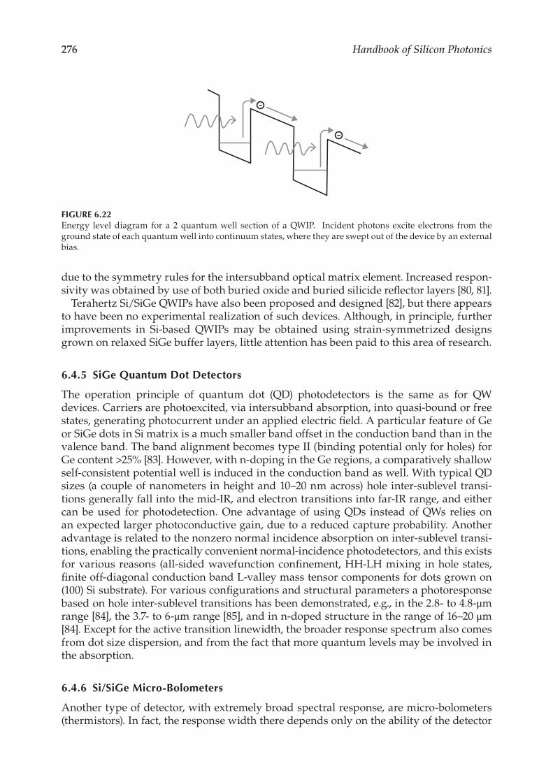
276 Handbook of Silicon Photonics
due to the symmetry rules for the intersubband optical matrix element. Increased respon-sivity was obtained by use of both buried oxide and buried silicide reflector layers [80, 81].
Terahertz Si/SiGe QWIPs have also been proposed and designed [82], but there appears to have been no experimental realization of such devices. Although, in principle, further improvements in Si-based QWIPs may be obtained using strain- symmetrized designs grown on relaxed SiGe buffer layers, little attention has been paid to this area of research.
6.4.5 SiGe Quantum Dot Detectors
The operation principle of quantum dot (QD) photodetectors is the same as for QW devices. Carriers are photoexcited, via intersubband absorption, into quasi-bound or free states, generating photocurrent under an applied electric field. A particular feature of Ge or SiGe dots in Si matrix is a much smaller band offset in the conduction band than in the valence band. The band alignment becomes type II (binding potential only for holes) for Ge content >25% [83]. However, with n-doping in the Ge regions, a comparatively shallow self-consistent potential well is induced in the conduction band as well. With typical QD sizes (a couple of nanometers in height and 10–20 nm across) hole inter-sublevel transi-tions generally fall into the mid-IR, and electron transitions into far-IR range, and either can be used for photodetection. One advantage of using QDs instead of QWs relies on an expected larger photoconductive gain, due to a reduced capture probability. Another advantage is related to the nonzero normal incidence absorption on inter-sublevel transi-tions, enabling the practically convenient normal-incidence photodetectors, and this exists for various reasons (all-sided wavefunction confinement, HH-LH mixing in hole states, finite off-diagonal conduction band L-valley mass tensor components for dots grown on (100) Si substrate). For various configurations and structural parameters a photoresponse based on hole inter-sublevel transitions has been demonstrated, e.g., in the 2.8- to 4.8-μm range [84], the 3.7- to 6-μm range [85], and in n-doped structure in the range of 16–20 μm [84]. Except for the active transition linewidth, the broader response spectrum also comes from dot size dispersion, and from the fact that more quantum levels may be involved in the absorption.
6.4.6 Si/SiGe Micro-Bolometers
Another type of detector, with extremely broad spectral response, are micro-bolometers (thermistors). In fact, the response width there depends only on the ability of the detector
-
-
FIGURE 6.22Energy level diagram for a 2 quantum well section of a QWIP. Incident photons excite electrons from the ground state of each quantum well into continuum states, where they are swept out of the device by an external bias.
277Long-Wavelength Photonic Circuits
structure to absorb incident radiation power and transfer it to the lattice. The operation of the SiGe/Si thermistor relies on thermal excitation of charge carriers from quantum-confined low-energy states, or carriers trapped at various defects, where they have low mobility, to free states where they are highly mobile. The temperature coefficient of resis-tance (TCR) increases with an increasing activation energy—the difference between the free and bound state energy—hence in SiGe QW or QD structures p-type doping is clearly much better than n-type. A high TCR favors larger Ge content and well width/dot size, which is limited by strain relaxation effects, and QDs are here advantageous over QWs. A TCR of approximately 3.0%/K has been obtained at room temperature in QWs with 32%Ge, while Ge QDs in a Si matrix offered a somewhat larger value of 3.4%/K, but with the noise factor increased by three orders of magnitude [86]. Amorphous SiGe:H-based bolometers, also compatible with the CMOS technology, have been successfully tested as detectors of terahertz radiation (at ~1 THz), although they have originally been designed for IR wavelengths [87].
6.4.7 Conclusions
Research activity in Si-based long-wavelength detectors has resulted in several different devices that have sufficiently good performance to be considered ready for use in silicon photonic circuits. Of these, the Si microbolometers are perhaps the most interesting devices for practical applications, because of their room temperature operation and compatibility with CMOS processing. The development of long wavelength Si-based lasers is still in relative infancy, with the only successful devices requiring optical pumping by large, high power sources, which effectively precludes their employment in integrated Si-photonic circuits. However, simulation work has shown that Si-based quantum cascade lasers that rely on intersubband transitions in n-type germanium quantum wells are more promising than any of the structures previously investigated experimentally.
6.5 Mid-Infrared Heterogeneous Integration
Gunther Roelkens
6.5.1 Introduction
Although silicon-based photonic integrated circuits are promising for passive optical functions in the short-wave and mid-IR, substantially more complex photonic integrated circuits could be realized if these waveguide structures could be co-integrated with pho-todetectors and light sources for SWIR/MIR. This could, for example, enable the realiza-tion of integrated spectroscopic chips, in which a silicon-based wavelength demultiplexer is combined with an integrated photodetector array. Or, it could enable the realization of integrated tunable laser sources for the SWIR/MIR, also a very useful component in spec-troscopic systems. Mid-IR spectroscopy has gained significant importance in recent years as a detection technique for substances that absorb in this spectral region. Traditionally, a spectroscopic system consists of bulky equipment that is difficult to handle and incurs high cost. An integrated spectroscopic system would eliminate these disadvantages.
GaSb-based active opto-electronic devices allow realization of mid-IR light sources and detectors in the 2- to 3-μm wavelength range for such integrated systems. Hence, the
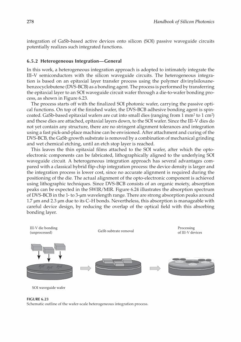
278 Handbook of Silicon Photonics
integration of GaSb-based active devices onto silicon (SOI) passive waveguide circuits potentially realizes such integrated functions.
6.5.2 Heterogeneous Integration—General
In this work, a heterogeneous integration approach is adopted to intimately integrate the III–V semiconductors with the silicon waveguide circuits. The heterogeneous integra-tion is based on an epitaxial layer transfer process using the polymer divinylsiloxane- benzocyclobutene (DVS-BCB) as a bonding agent. The process is performed by transferring the epitaxial layer to an SOI waveguide circuit wafer through a die-to-wafer bonding pro-cess, as shown in Figure 6.23.
The process starts off with the finalized SOI photonic wafer, carrying the passive opti-cal functions. On top of the finished wafer, the DVS-BCB adhesive bonding agent is spin-coated. GaSb-based epitaxial wafers are cut into small dies (ranging from 1 mm2 to 1 cm2) and these dies are attached, epitaxial layers down, to the SOI wafer. Since the III–V dies do not yet contain any structure, there are no stringent alignment tolerances and integration using a fast pick-and-place machine can be envisioned. After attachment and curing of the DVS-BCB, the GaSb growth substrate is removed by a combination of mechanical grinding and wet chemical etching, until an etch stop layer is reached.
This leaves the thin epitaxial films attached to the SOI wafer, after which the opto-electronic components can be fabricated, lithographically aligned to the underlying SOI waveguide circuit. A heterogeneous integration approach has several advantages com-pared with a classical hybrid flip-chip integration process: the device density is larger and the integration process is lower cost, since no accurate alignment is required during the positioning of the die. The actual alignment of the opto-electronic component is achieved using lithographic techniques. Since DVS-BCB consists of an organic moiety, absorption peaks can be expected in the SWIR/MIR. Figure 6.24 illustrates the absorption spectrum of DVS-BCB in the 1- to 3-μm wavelength range. There are strong absorption peaks around 1.7 μm and 2.3 μm due to its C–H bonds. Nevertheless, this absorption is manageable with careful device design, by reducing the overlap of the optical field with this absorbing bonding layer.
III-V die bonding(unprocessed) GaSb subtrate removal
Processingof III-V devices
SOI waveguide wafer
FIGURE 6.23Schematic outline of the wafer-scale heterogeneous integration process.
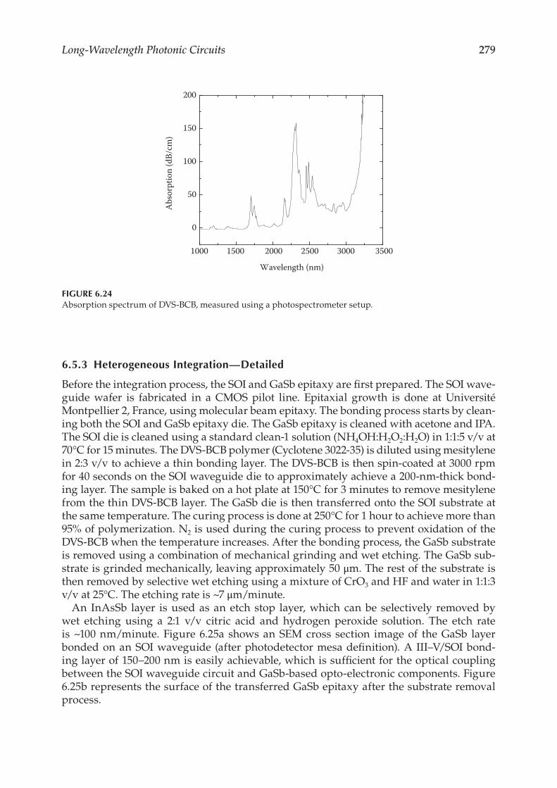
279Long-Wavelength Photonic Circuits
6.5.3 Heterogeneous Integration—Detailed
Before the integration process, the SOI and GaSb epitaxy are first prepared. The SOI wave-guide wafer is fabricated in a CMOS pilot line. Epitaxial growth is done at Université Montpellier 2, France, using molecular beam epitaxy. The bonding process starts by clean-ing both the SOI and GaSb epitaxy die. The GaSb epitaxy is cleaned with acetone and IPA. The SOI die is cleaned using a standard clean-1 solution (NH4OH:H2O2:H2O) in 1:1:5 v/v at 70°C for 15 minutes. The DVS-BCB polymer (Cyclotene 3022-35) is diluted using mesitylene in 2:3 v/v to achieve a thin bonding layer. The DVS-BCB is then spin-coated at 3000 rpm for 40 seconds on the SOI waveguide die to approximately achieve a 200-nm-thick bond-ing layer. The sample is baked on a hot plate at 150°C for 3 minutes to remove mesitylene from the thin DVS-BCB layer. The GaSb die is then transferred onto the SOI substrate at the same temperature. The curing process is done at 250°C for 1 hour to achieve more than 95% of polymerization. N2 is used during the curing process to prevent oxidation of the DVS-BCB when the temperature increases. After the bonding process, the GaSb substrate is removed using a combination of mechanical grinding and wet etching. The GaSb sub-strate is grinded mechanically, leaving approximately 50 μm. The rest of the substrate is then removed by selective wet etching using a mixture of CrO3 and HF and water in 1:1:3 v/v at 25°C. The etching rate is ~7 μm/minute.
An InAsSb layer is used as an etch stop layer, which can be selectively removed by wet etching using a 2:1 v/v citric acid and hydrogen peroxide solution. The etch rate is ~100 nm/minute. Figure 6.25a shows an SEM cross section image of the GaSb layer bonded on an SOI waveguide (after photodetector mesa definition). A III–V/SOI bond-ing layer of 150–200 nm is easily achievable, which is sufficient for the optical coupling between the SOI waveguide circuit and GaSb-based opto-electronic components. Figure 6.25b represents the surface of the transferred GaSb epitaxy after the substrate removal process.
1000 1500 2000 2500 3000 3500
0
50
100
150
200
Abs
orpt
ion
(dB/
cm)
Wavelength (nm)
FIGURE 6.24Absorption spectrum of DVS-BCB, measured using a photospectrometer setup.
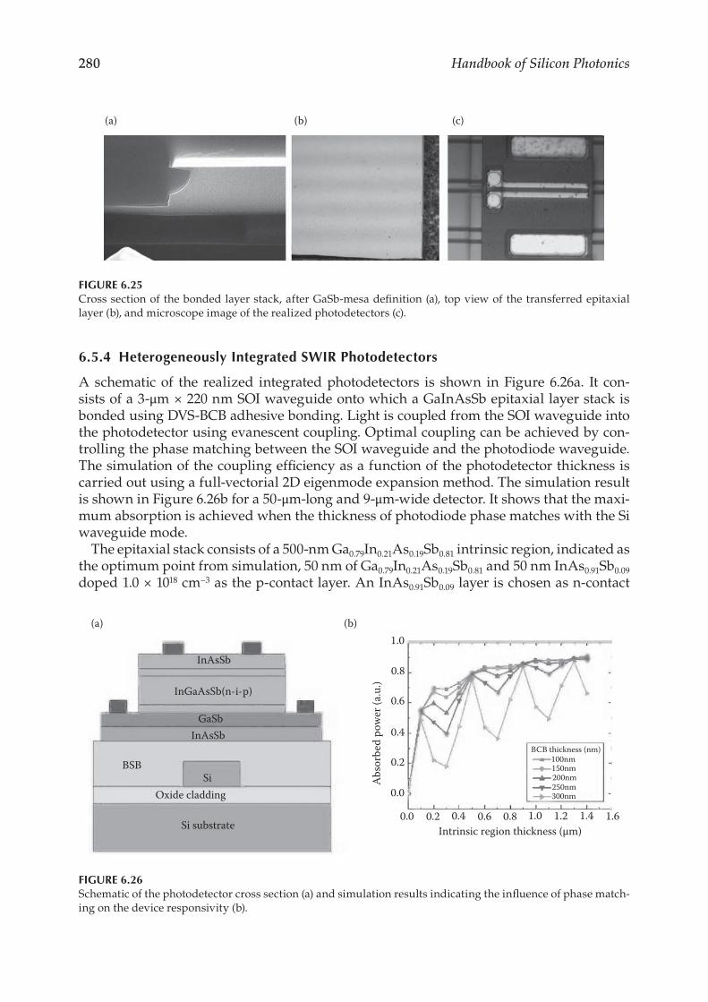
280 Handbook of Silicon Photonics
6.5.4 Heterogeneously Integrated SWIR Photodetectors
A schematic of the realized integrated photodetectors is shown in Figure 6.26a. It con-sists of a 3-μm × 220 nm SOI waveguide onto which a GaInAsSb epitaxial layer stack is bonded using DVS-BCB adhesive bonding. Light is coupled from the SOI waveguide into the photodetector using evanescent coupling. Optimal coupling can be achieved by con-trolling the phase matching between the SOI waveguide and the photodiode waveguide. The simulation of the coupling efficiency as a function of the photodetector thickness is carried out using a full-vectorial 2D eigenmode expansion method. The simulation result is shown in Figure 6.26b for a 50-μm-long and 9-μm-wide detector. It shows that the maxi-mum absorption is achieved when the thickness of photodiode phase matches with the Si waveguide mode.
The epitaxial stack consists of a 500-nm Ga0.79In0.21As0.19Sb0.81 intrinsic region, indicated as the optimum point from simulation, 50 nm of Ga0.79In0.21As0.19Sb0.81 and 50 nm InAs0.91Sb0.09
doped 1.0 × 1018 cm−3 as the p-contact layer. An InAs0.91Sb0.09 layer is chosen as n-contact
(a) (b) (c)
FIGURE 6.25Cross section of the bonded layer stack, after GaSb-mesa definition (a), top view of the transferred epitaxial layer (b), and microscope image of the realized photodetectors (c).
Intrinsic region thickness (μm)0.0 0.2 0.4 0.6 0.8 1.0 1.2 1.4 1.6
BCB thickness (nm)100nm150nm200nm250nm300nm
1.0(a) (b)
0.8
0.6
0.4
0.2
0.0
Abs
orbe
d po
wer
(a.u
.)
InAsSb
InGaAsSb(n-i-p)
GaSbInAsSb
BSBSi
Oxide cladding
Si substrate
FIGURE 6.26Schematic of the photodetector cross section (a) and simulation results indicating the influence of phase match-ing on the device responsivity (b).
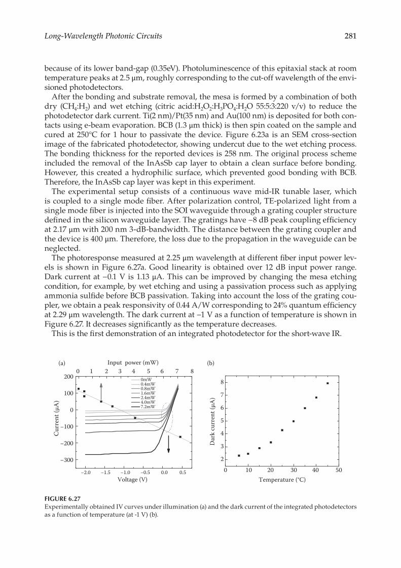
281Long-Wavelength Photonic Circuits
because of its lower band-gap (0.35eV). Photoluminescence of this epitaxial stack at room temperature peaks at 2.5 μm, roughly corresponding to the cut-off wavelength of the envi-sioned photodetectors.
After the bonding and substrate removal, the mesa is formed by a combination of both dry (CH4:H2) and wet etching (citric acid:H2O2:H3PO4:H2O 55:5:3:220 v/v) to reduce the photo detector dark current. Ti(2 nm)/Pt(35 nm) and Au(100 nm) is deposited for both con-tacts using e-beam evaporation. BCB (1.3 μm thick) is then spin coated on the sample and cured at 250°C for 1 hour to passivate the device. Figure 6.23a is an SEM cross-section image of the fabricated photodetector, showing undercut due to the wet etching process. The bonding thickness for the reported devices is 258 nm. The original process scheme included the removal of the InAsSb cap layer to obtain a clean surface before bonding. However, this created a hydrophilic surface, which prevented good bonding with BCB. Therefore, the InAsSb cap layer was kept in this experiment.
The experimental setup consists of a continuous wave mid-IR tunable laser, which is coupled to a single mode fiber. After polarization control, TE-polarized light from a single mode fiber is injected into the SOI waveguide through a grating coupler structure defined in the silicon waveguide layer. The gratings have −8 dB peak coupling efficiency at 2.17 μm with 200 nm 3-dB-bandwidth. The distance between the grating coupler and the device is 400 μm. Therefore, the loss due to the propagation in the waveguide can be neglected.
The photoresponse measured at 2.25 μm wavelength at different fiber input power lev-els is shown in Figure 6.27a. Good linearity is obtained over 12 dB input power range. Dark current at −0.1 V is 1.13 μA. This can be improved by changing the mesa etching condition, for example, by wet etching and using a passivation process such as applying ammonia sulfide before BCB passivation. Taking into account the loss of the grating cou-pler, we obtain a peak responsivity of 0.44 A/W corresponding to 24% quantum efficiency at 2.29 μm wavelength. The dark current at −1 V as a function of temperature is shown in Figure 6.27. It decreases significantly as the temperature decreases.
This is the first demonstration of an integrated photodetector for the short-wave IR.
−2.0 −1.5 −1.0 −0.5 0.0 0.5
−300
−200
−100
0
100
2000 1 2 3 4 5 6 7 8
Cur
rent
(μA
)
Voltage (V)
0mW 0.4mW 0.8mW 1.6mW 2.4mW 4.0mW 7.2mW
Input power (mW)
0 10 20 30 40 50
2
3
4
5
6
7
8
Dar
k cu
rren
t (μΑ
)
Temperature (°C)
(a) (b)
FIGURE 6.27Experimentally obtained IV curves under illumination (a) and the dark current of the integrated photodetectors as a function of temperature (at -1 V) (b).
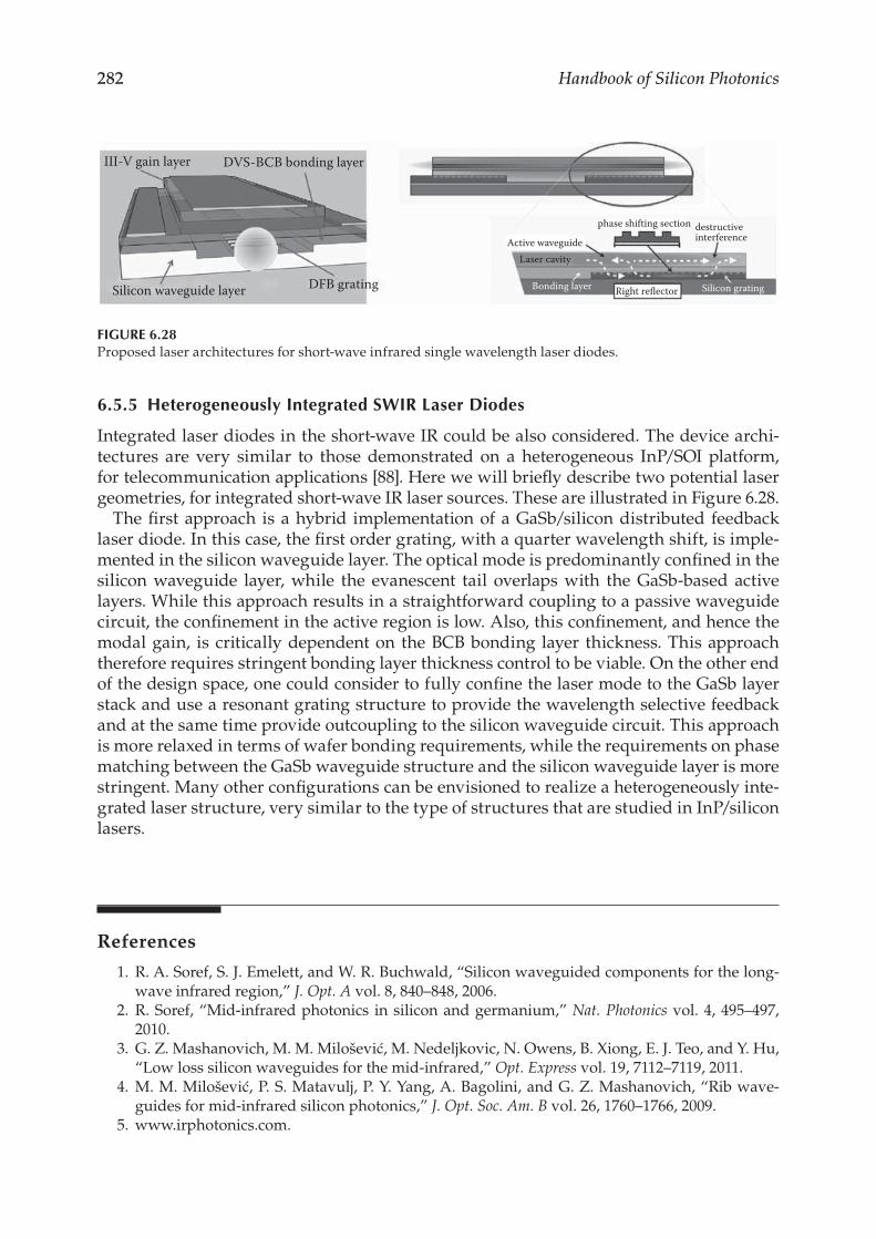
282 Handbook of Silicon Photonics
6.5.5 Heterogeneously Integrated SWIR Laser Diodes
Integrated laser diodes in the short-wave IR could be also considered. The device archi-tectures are very similar to those demonstrated on a heterogeneous InP/SOI platform, for telecommunication applications [88]. Here we will briefly describe two potential laser geometries, for integrated short-wave IR laser sources. These are illustrated in Figure 6.28.
The first approach is a hybrid implementation of a GaSb/silicon distributed feedback laser diode. In this case, the first order grating, with a quarter wavelength shift, is imple-mented in the silicon waveguide layer. The optical mode is predominantly confined in the silicon waveguide layer, while the evanescent tail overlaps with the GaSb-based active layers. While this approach results in a straightforward coupling to a passive waveguide circuit, the confinement in the active region is low. Also, this confinement, and hence the modal gain, is critically dependent on the BCB bonding layer thickness. This approach therefore requires stringent bonding layer thickness control to be viable. On the other end of the design space, one could consider to fully confine the laser mode to the GaSb layer stack and use a resonant grating structure to provide the wavelength selective feedback and at the same time provide outcoupling to the silicon waveguide circuit. This approach is more relaxed in terms of wafer bonding requirements, while the requirements on phase matching between the GaSb waveguide structure and the silicon waveguide layer is more stringent. Many other configurations can be envisioned to realize a heterogeneously inte-grated laser structure, very similar to the type of structures that are studied in InP/silicon lasers.
References
1. R. A. Soref, S. J. Emelett, and W. R. Buchwald, “Silicon waveguided components for the long-wave infrared region,” J. Opt. A vol. 8, 840–848, 2006.
2. R. Soref, “Mid-infrared photonics in silicon and germanium,” Nat. Photonics vol. 4, 495–497, 2010.
3. G. Z. Mashanovich, M. M. Milošević, M. Nedeljkovic, N. Owens, B. Xiong, E. J. Teo, and Y. Hu, “Low loss silicon waveguides for the mid-infrared,” Opt. Express vol. 19, 7112–7119, 2011.
4. M. M. Milošević, P. S. Matavulj, P. Y. Yang, A. Bagolini, and G. Z. Mashanovich, “Rib wave-guides for mid-infrared silicon photonics,” J. Opt. Soc. Am. B vol. 26, 1760–1766, 2009.
5. www.irphotonics.com.
III-V gain layer DVS-BCB bonding layer
Silicon waveguide layer DFB grating Right reflector Silicon gratingBonding layer
Laser cavityActive waveguide
phase shifting section destructiveinterference
FIGURE 6.28Proposed laser architectures for short-wave infrared single wavelength laser diodes.
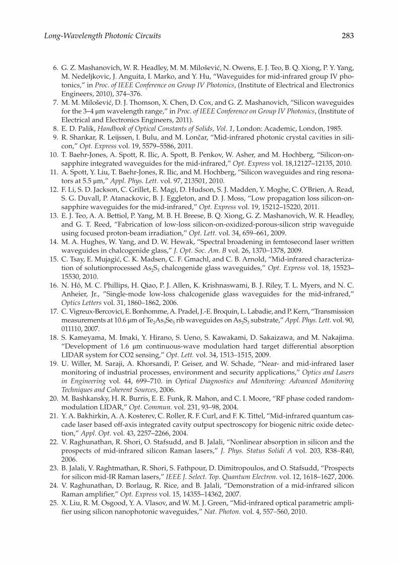
283Long-Wavelength Photonic Circuits
6. G. Z. Mashanovich, W. R. Headley, M. M. Milošević, N. Owens, E. J. Teo, B. Q. Xiong, P. Y. Yang, M. Nedeljkovic, J. Anguita, I. Marko, and Y. Hu, “Waveguides for mid-infrared group IV pho-tonics,” in Proc. of IEEE Conference on Group IV Photonics, (Institute of Electrical and Electronics Engineers, 2010), 374–376.
7. M. M. Milošević, D. J. Thomson, X. Chen, D. Cox, and G. Z. Mashanovich, “Silicon waveguides for the 3–4 μm wavelength range,” in Proc. of IEEE Conference on Group IV Photonics, (Institute of Electrical and Electronics Engineers, 2011).
8. E. D. Palik, Handbook of Optical Constants of Solids, Vol. 1, London: Academic, London, 1985. 9. R. Shankar, R. Leijssen, I. Bulu, and M. Lončar, “Mid-infrared photonic crystal cavities in sili-
con,” Opt. Express vol. 19, 5579–5586, 2011. 10. T. Baehr-Jones, A. Spott, R. Ilic, A. Spott, B. Penkov, W. Asher, and M. Hochberg, “Silicon-on-
sapphire integrated waveguides for the mid-infrared,” Opt. Express vol. 18,12127–12135, 2010. 11. A. Spott, Y. Liu, T. Baehr-Jones, R. Ilic, and M. Hochberg, “Silicon waveguides and ring resona-
tors at 5.5 μm,” Appl. Phys. Lett. vol. 97, 213501, 2010. 12. F. Li, S. D. Jackson, C. Grillet, E. Magi, D. Hudson, S. J. Madden, Y. Moghe, C. O’Brien, A. Read,
S. G. Duvall, P. Atanackovic, B. J. Eggleton, and D. J. Moss, “Low propagation loss silicon-on-sapphire waveguides for the mid-infrared,” Opt. Express vol. 19, 15212–15220, 2011.
13. E. J. Teo, A. A. Bettiol, P. Yang, M. B. H. Breese, B. Q. Xiong, G. Z. Mashanovich, W. R. Headley, and G. T. Reed, “Fabrication of low-loss silicon-on-oxidized-porous-silicon strip waveguide using focused proton-beam irradiation,” Opt. Lett. vol. 34, 659–661, 2009.
14. M. A. Hughes, W. Yang, and D. W. Hewak, “Spectral broadening in femtosecond laser written waveguides in chalcogenide glass,” J. Opt. Soc. Am. B vol. 26, 1370–1378, 2009.
15. C. Tsay, E. Mujagić, C. K. Madsen, C. F. Gmachl, and C. B. Arnold, “Mid-infrared characteriza-tion of solutionprocessed As2S3 chalcogenide glass waveguides,” Opt. Express vol. 18, 15523–15530, 2010.
16. N. Hô, M. C. Phillips, H. Qiao, P. J. Allen, K. Krishnaswami, B. J. Riley, T. L. Myers, and N. C. Anheier, Jr., ”Single-mode low-loss chalcogenide glass waveguides for the mid-infrared,” Optics Letters vol. 31, 1860–1862, 2006.
17. C. Vigreux-Bercovici, E. Bonhomme, A. Pradel, J.-E. Broquin, L. Labadie, and P. Kern, “Transmission measurements at 10.6 μm of Te2As3Se5 rib waveguides on As2S3 substrate,” Appl. Phys. Lett. vol. 90, 011110, 2007.
18. S. Kameyama, M. Imaki, Y. Hirano, S. Ueno, S. Kawakami, D. Sakaizawa, and M. Nakajima. “Development of 1.6 μm continuous-wave modulation hard target differential absorption LIDAR system for CO2 sensing,” Opt. Lett. vol. 34, 1513–1515, 2009.
19. U. Willer, M. Saraji, A. Khorsandi, P. Geiser, and W. Schade, “Near- and mid-infrared laser monitoring of industrial processes, environment and security applications,” Optics and Lasers in Engineering vol. 44, 699–710. in Optical Diagnostics and Monitoring: Advanced Monitoring Techniques and Coherent Sources, 2006.
20. M. Bashkansky, H. R. Burris, E. E. Funk, R. Mahon, and C. I. Moore, “RF phase coded random-modulation LIDAR,” Opt. Commun. vol. 231, 93–98, 2004.
21. Y. A. Bakhirkin, A. A. Kosterev, C. Roller, R. F. Curl, and F. K. Tittel, “Mid-infrared quantum cas-cade laser based off-axis integrated cavity output spectroscopy for biogenic nitric oxide detec-tion,” Appl. Opt. vol. 43, 2257–2266, 2004.
22. V. Raghunathan, R. Shori, O. Stafsudd, and B. Jalali, “Nonlinear absorption in silicon and the prospects of mid-infrared silicon Raman lasers,” J. Phys. Status Solidi A vol. 203, R38–R40, 2006.
23. B. Jalali, V. Raghtmathan, R. Shori, S. Fathpour, D. Dimitropoulos, and O. Stafsudd, “Prospects for silicon mid-IR Raman lasers,” IEEE J. Select. Top. Quantum Electron. vol. 12, 1618–1627, 2006.
24. V. Raghunathan, D. Borlaug, R. Rice, and B. Jalali, “Demonstration of a mid-infrared silicon Raman amplifier,” Opt. Express vol. 15, 14355–14362, 2007.
25. X. Liu, R. M. Osgood, Y. A. Vlasov, and W. M. J. Green, “Mid-infrared optical parametric ampli-fier using silicon nanophotonic waveguides,” Nat. Photon. vol. 4, 557–560, 2010.
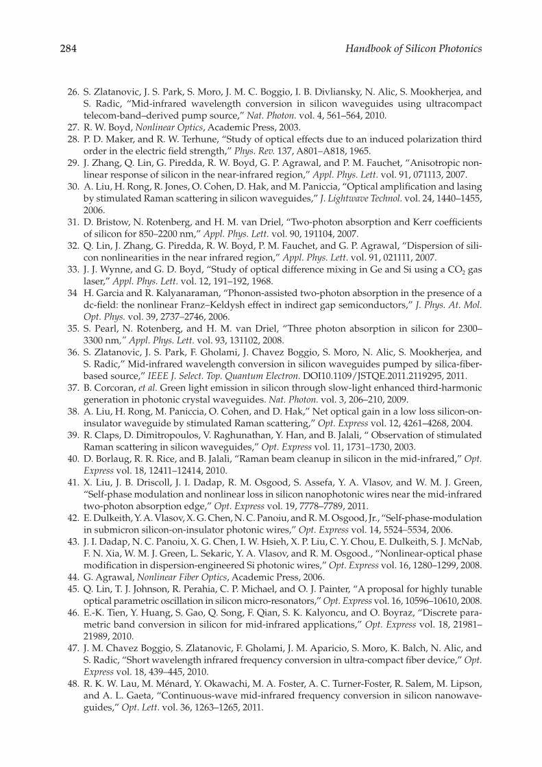
284 Handbook of Silicon Photonics
26. S. Zlatanovic, J. S. Park, S. Moro, J. M. C. Boggio, I. B. Divliansky, N. Alic, S. Mookherjea, and S. Radic, “Mid-infrared wavelength conversion in silicon waveguides using ultracompact telecom- band–derived pump source,” Nat. Photon. vol. 4, 561–564, 2010.
27. R. W. Boyd, Nonlinear Optics, Academic Press, 2003. 28. P. D. Maker, and R. W. Terhune, “Study of optical effects due to an induced polarization third
order in the electric field strength,” Phys. Rev. 137, A801–A818, 1965. 29. J. Zhang, Q. Lin, G. Piredda, R. W. Boyd, G. P. Agrawal, and P. M. Fauchet, “Anisotropic non-
linear response of silicon in the near-infrared region,” Appl. Phys. Lett. vol. 91, 071113, 2007. 30. A. Liu, H. Rong, R. Jones, O. Cohen, D. Hak, and M. Paniccia, “Optical amplification and lasing
by stimulated Raman scattering in silicon waveguides,” J. Lightwave Technol. vol. 24, 1440–1455, 2006.
31. D. Bristow, N. Rotenberg, and H. M. van Driel, “Two-photon absorption and Kerr coefficients of silicon for 850–2200 nm,” Appl. Phys. Lett. vol. 90, 191104, 2007.
32. Q. Lin, J. Zhang, G. Piredda, R. W. Boyd, P. M. Fauchet, and G. P. Agrawal, “Dispersion of sili-con nonlinearities in the near infrared region,” Appl. Phys. Lett. vol. 91, 021111, 2007.
33. J. J. Wynne, and G. D. Boyd, “Study of optical difference mixing in Ge and Si using a CO2 gas laser,” Appl. Phys. Lett. vol. 12, 191–192, 1968.
34 H. Garcia and R. Kalyanaraman, “Phonon-assisted two-photon absorption in the presence of a dc-field: the nonlinear Franz–Keldysh effect in indirect gap semiconductors,” J. Phys. At. Mol. Opt. Phys. vol. 39, 2737–2746, 2006.
35. S. Pearl, N. Rotenberg, and H. M. van Driel, “Three photon absorption in silicon for 2300–3300 nm,” Appl. Phys. Lett. vol. 93, 131102, 2008.
36. S. Zlatanovic, J. S. Park, F. Gholami, J. Chavez Boggio, S. Moro, N. Alic, S. Mookherjea, and S. Radic,” Mid-infrared wavelength conversion in silicon waveguides pumped by silica-fiber-based source,” IEEE J. Select. Top. Quantum Electron. DOI10.1109/JSTQE.2011.2119295, 2011.
37. B. Corcoran, et al. Green light emission in silicon through slow-light enhanced third-harmonic generation in photonic crystal waveguides. Nat. Photon. vol. 3, 206–210, 2009.
38. A. Liu, H. Rong, M. Paniccia, O. Cohen, and D. Hak,” Net optical gain in a low loss silicon-on-insulator waveguide by stimulated Raman scattering,” Opt. Express vol. 12, 4261–4268, 2004.
39. R. Claps, D. Dimitropoulos, V. Raghunathan, Y. Han, and B. Jalali, “ Observation of stimulated Raman scattering in silicon waveguides,” Opt. Express vol. 11, 1731–1730, 2003.
40. D. Borlaug, R. R. Rice, and B. Jalali, “Raman beam cleanup in silicon in the mid-infrared,” Opt. Express vol. 18, 12411–12414, 2010.
41. X. Liu, J. B. Driscoll, J. I. Dadap, R. M. Osgood, S. Assefa, Y. A. Vlasov, and W. M. J. Green, “Self-phase modulation and nonlinear loss in silicon nanophotonic wires near the mid-infrared two-photon absorption edge,” Opt. Express vol. 19, 7778–7789, 2011.
42. E. Dulkeith, Y. A. Vlasov, X. G. Chen, N. C. Panoiu, and R. M. Osgood, Jr., “Self-phase-modulation in submicron silicon-on-insulator photonic wires,” Opt. Express vol. 14, 5524–5534, 2006.
43. J. I. Dadap, N. C. Panoiu, X. G. Chen, I. W. Hsieh, X. P. Liu, C. Y. Chou, E. Dulkeith, S. J. McNab, F. N. Xia, W. M. J. Green, L. Sekaric, Y. A. Vlasov, and R. M. Osgood., “Nonlinear-optical phase modification in dispersion-engineered Si photonic wires,” Opt. Express vol. 16, 1280–1299, 2008.
44. G. Agrawal, Nonlinear Fiber Optics, Academic Press, 2006. 45. Q. Lin, T. J. Johnson, R. Perahia, C. P. Michael, and O. J. Painter, “A proposal for highly tunable
optical parametric oscillation in silicon micro-resonators,” Opt. Express vol. 16, 10596–10610, 2008. 46. E.-K. Tien, Y. Huang, S. Gao, Q. Song, F. Qian, S. K. Kalyoncu, and O. Boyraz, “Discrete para-
metric band conversion in silicon for mid-infrared applications,” Opt. Express vol. 18, 21981–21989, 2010.
47. J. M. Chavez Boggio, S. Zlatanovic, F. Gholami, J. M. Aparicio, S. Moro, K. Balch, N. Alic, and S. Radic, “Short wavelength infrared frequency conversion in ultra-compact fiber device,” Opt. Express vol. 18, 439–445, 2010.
48. R. K. W. Lau, M. Ménard, Y. Okawachi, M. A. Foster, A. C. Turner-Foster, R. Salem, M. Lipson, and A. L. Gaeta, “Continuous-wave mid-infrared frequency conversion in silicon nanowave-guides,” Opt. Lett. vol. 36, 1263–1265, 2011.
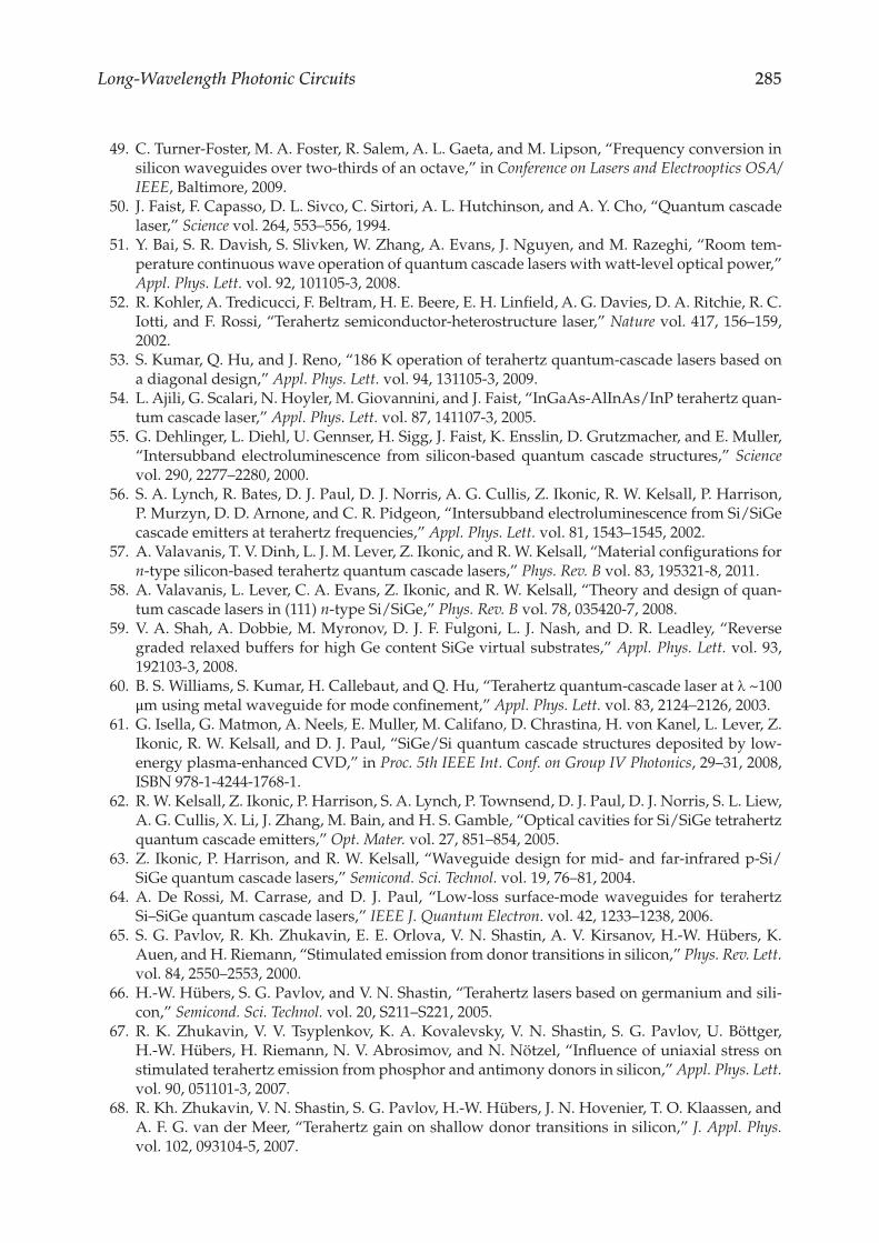
285Long-Wavelength Photonic Circuits
49. C. Turner-Foster, M. A. Foster, R. Salem, A. L. Gaeta, and M. Lipson, “Frequency conversion in silicon waveguides over two-thirds of an octave,” in Conference on Lasers and Electrooptics OSA/IEEE, Baltimore, 2009.
50. J. Faist, F. Capasso, D. L. Sivco, C. Sirtori, A. L. Hutchinson, and A. Y. Cho, “Quantum cascade laser,” Science vol. 264, 553–556, 1994.
51. Y. Bai, S. R. Davish, S. Slivken, W. Zhang, A. Evans, J. Nguyen, and M. Razeghi, “Room tem-perature continuous wave operation of quantum cascade lasers with watt-level optical power,” Appl. Phys. Lett. vol. 92, 101105-3, 2008.
52. R. Kohler, A. Tredicucci, F. Beltram, H. E. Beere, E. H. Linfield, A. G. Davies, D. A. Ritchie, R. C. Iotti, and F. Rossi, “Terahertz semiconductor-heterostructure laser,” Nature vol. 417, 156–159, 2002.
53. S. Kumar, Q. Hu, and J. Reno, “186 K operation of terahertz quantum-cascade lasers based on a diagonal design,” Appl. Phys. Lett. vol. 94, 131105-3, 2009.
54. L. Ajili, G. Scalari, N. Hoyler, M. Giovannini, and J. Faist, “InGaAs-AlInAs/InP terahertz quan-tum cascade laser,” Appl. Phys. Lett. vol. 87, 141107-3, 2005.
55. G. Dehlinger, L. Diehl, U. Gennser, H. Sigg, J. Faist, K. Ensslin, D. Grutzmacher, and E. Muller, “Intersubband electroluminescence from silicon-based quantum cascade structures,” Science vol. 290, 2277–2280, 2000.
56. S. A. Lynch, R. Bates, D. J. Paul, D. J. Norris, A. G. Cullis, Z. Ikonic, R. W. Kelsall, P. Harrison, P. Murzyn, D. D. Arnone, and C. R. Pidgeon, “Intersubband electroluminescence from Si/SiGe cascade emitters at terahertz frequencies,” Appl. Phys. Lett. vol. 81, 1543–1545, 2002.
57. A. Valavanis, T. V. Dinh, L. J. M. Lever, Z. Ikonic, and R. W. Kelsall, “Material configurations for n-type silicon-based terahertz quantum cascade lasers,” Phys. Rev. B vol. 83, 195321-8, 2011.
58. A. Valavanis, L. Lever, C. A. Evans, Z. Ikonic, and R. W. Kelsall, “Theory and design of quan-tum cascade lasers in (111) n-type Si/SiGe,” Phys. Rev. B vol. 78, 035420-7, 2008.
59. V. A. Shah, A. Dobbie, M. Myronov, D. J. F. Fulgoni, L. J. Nash, and D. R. Leadley, “Reverse graded relaxed buffers for high Ge content SiGe virtual substrates,” Appl. Phys. Lett. vol. 93, 192103-3, 2008.
60. B. S. Williams, S. Kumar, H. Callebaut, and Q. Hu, “Terahertz quantum-cascade laser at λ ~100 μm using metal waveguide for mode confinement,” Appl. Phys. Lett. vol. 83, 2124–2126, 2003.
61. G. Isella, G. Matmon, A. Neels, E. Muller, M. Califano, D. Chrastina, H. von Kanel, L. Lever, Z. Ikonic, R. W. Kelsall, and D. J. Paul, “SiGe/Si quantum cascade structures deposited by low-energy plasma-enhanced CVD,” in Proc. 5th IEEE Int. Conf. on Group IV Photonics, 29–31, 2008, ISBN 978-1-4244-1768-1.
62. R. W. Kelsall, Z. Ikonic, P. Harrison, S. A. Lynch, P. Townsend, D. J. Paul, D. J. Norris, S. L. Liew, A. G. Cullis, X. Li, J. Zhang, M. Bain, and H. S. Gamble, “Optical cavities for Si/SiGe tetrahertz quantum cascade emitters,” Opt. Mater. vol. 27, 851–854, 2005.
63. Z. Ikonic, P. Harrison, and R. W. Kelsall, “Waveguide design for mid- and far-infrared p-Si/SiGe quantum cascade lasers,” Semicond. Sci. Technol. vol. 19, 76–81, 2004.
64. A. De Rossi, M. Carrase, and D. J. Paul, “Low-loss surface-mode waveguides for terahertz Si–SiGe quantum cascade lasers,” IEEE J. Quantum Electron. vol. 42, 1233–1238, 2006.
65. S. G. Pavlov, R. Kh. Zhukavin, E. E. Orlova, V. N. Shastin, A. V. Kirsanov, H.-W. Hübers, K. Auen, and H. Riemann, “Stimulated emission from donor transitions in silicon,” Phys. Rev. Lett. vol. 84, 2550–2553, 2000.
66. H.-W. Hübers, S. G. Pavlov, and V. N. Shastin, “Terahertz lasers based on germanium and sili-con,” Semicond. Sci. Technol. vol. 20, S211–S221, 2005.
67. R. K. Zhukavin, V. V. Tsyplenkov, K. A. Kovalevsky, V. N. Shastin, S. G. Pavlov, U. Böttger, H.-W. Hübers, H. Riemann, N. V. Abrosimov, and N. Nötzel, “Influence of uniaxial stress on stimulated terahertz emission from phosphor and antimony donors in silicon,” Appl. Phys. Lett. vol. 90, 051101-3, 2007.
68. R. Kh. Zhukavin, V. N. Shastin, S. G. Pavlov, H.-W. Hübers, J. N. Hovenier, T. O. Klaassen, and A. F. G. van der Meer, “Terahertz gain on shallow donor transitions in silicon,” J. Appl. Phys. vol. 102, 093104-5, 2007.
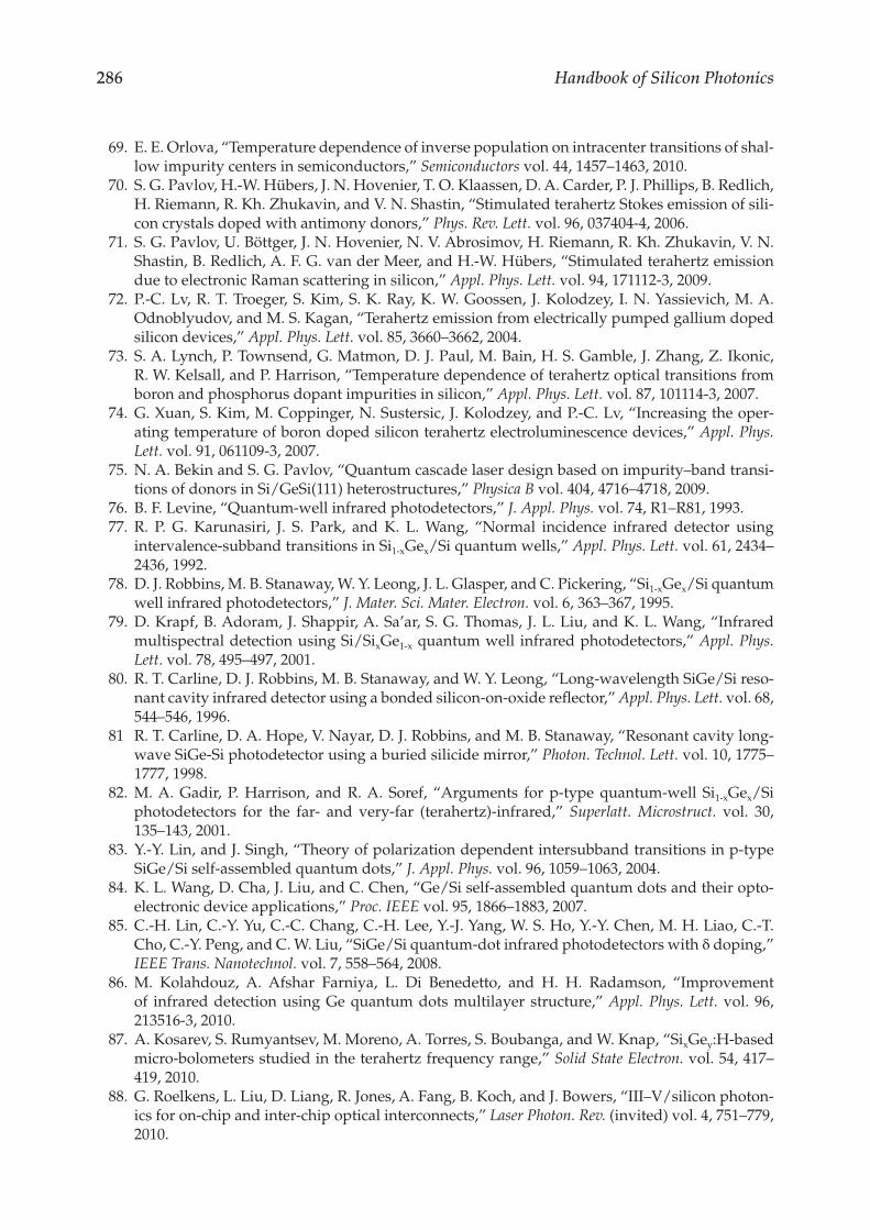
286 Handbook of Silicon Photonics
69. E. E. Orlova, “Temperature dependence of inverse population on intracenter transitions of shal-low impurity centers in semiconductors,” Semiconductors vol. 44, 1457–1463, 2010.
70. S. G. Pavlov, H.-W. Hübers, J. N. Hovenier, T. O. Klaassen, D. A. Carder, P. J. Phillips, B. Redlich, H. Riemann, R. Kh. Zhukavin, and V. N. Shastin, “Stimulated terahertz Stokes emission of sili-con crystals doped with antimony donors,” Phys. Rev. Lett. vol. 96, 037404-4, 2006.
71. S. G. Pavlov, U. Böttger, J. N. Hovenier, N. V. Abrosimov, H. Riemann, R. Kh. Zhukavin, V. N. Shastin, B. Redlich, A. F. G. van der Meer, and H.-W. Hübers, “Stimulated terahertz emission due to electronic Raman scattering in silicon,” Appl. Phys. Lett. vol. 94, 171112-3, 2009.
72. P.-C. Lv, R. T. Troeger, S. Kim, S. K. Ray, K. W. Goossen, J. Kolodzey, I. N. Yassievich, M. A. Odnoblyudov, and M. S. Kagan, “Terahertz emission from electrically pumped gallium doped silicon devices,” Appl. Phys. Lett. vol. 85, 3660–3662, 2004.
73. S. A. Lynch, P. Townsend, G. Matmon, D. J. Paul, M. Bain, H. S. Gamble, J. Zhang, Z. Ikonic, R. W. Kelsall, and P. Harrison, “Temperature dependence of terahertz optical transitions from boron and phosphorus dopant impurities in silicon,” Appl. Phys. Lett. vol. 87, 101114-3, 2007.
74. G. Xuan, S. Kim, M. Coppinger, N. Sustersic, J. Kolodzey, and P.-C. Lv, “Increasing the oper-ating temperature of boron doped silicon terahertz electroluminescence devices,” Appl. Phys. Lett. vol. 91, 061109-3, 2007.
75. N. A. Bekin and S. G. Pavlov, “Quantum cascade laser design based on impurity–band transi-tions of donors in Si/GeSi(111) heterostructures,” Physica B vol. 404, 4716–4718, 2009.
76. B. F. Levine, “Quantum-well infrared photodetectors,” J. Appl. Phys. vol. 74, R1–R81, 1993. 77. R. P. G. Karunasiri, J. S. Park, and K. L. Wang, “Normal incidence infrared detector using
intervalence -subband transitions in Si1-xGex/Si quantum wells,” Appl. Phys. Lett. vol. 61, 2434–2436, 1992.
78. D. J. Robbins, M. B. Stanaway, W. Y. Leong, J. L. Glasper, and C. Pickering, “Si1-xGex/Si quantum well infrared photodetectors,” J. Mater. Sci. Mater. Electron. vol. 6, 363–367, 1995.
79. D. Krapf, B. Adoram, J. Shappir, A. Sa’ar, S. G. Thomas, J. L. Liu, and K. L. Wang, “Infrared multispectral detection using Si/SixGe1-x quantum well infrared photodetectors,” Appl. Phys. Lett. vol. 78, 495–497, 2001.
80. R. T. Carline, D. J. Robbins, M. B. Stanaway, and W. Y. Leong, “Long-wavelength SiGe/Si reso-nant cavity infrared detector using a bonded silicon-on-oxide reflector,” Appl. Phys. Lett. vol. 68, 544–546, 1996.
81 R. T. Carline, D. A. Hope, V. Nayar, D. J. Robbins, and M. B. Stanaway, “Resonant cavity long-wave SiGe-Si photodetector using a buried silicide mirror,” Photon. Technol. Lett. vol. 10, 1775–1777, 1998.
82. M. A. Gadir, P. Harrison, and R. A. Soref, “Arguments for p-type quantum-well Si1-xGex/Si photodetectors for the far- and very-far (terahertz)-infrared,” Superlatt. Microstruct. vol. 30, 135–143, 2001.
83. Y.-Y. Lin, and J. Singh, “Theory of polarization dependent intersubband transitions in p-type SiGe/Si self-assembled quantum dots,” J. Appl. Phys. vol. 96, 1059–1063, 2004.
84. K. L. Wang, D. Cha, J. Liu, and C. Chen, “Ge/Si self-assembled quantum dots and their opto-electronic device applications,” Proc. IEEE vol. 95, 1866–1883, 2007.
85. C.-H. Lin, C.-Y. Yu, C.-C. Chang, C.-H. Lee, Y.-J. Yang, W. S. Ho, Y.-Y. Chen, M. H. Liao, C.-T. Cho, C.-Y. Peng, and C. W. Liu, “SiGe/Si quantum-dot infrared photodetectors with δ doping,” IEEE Trans. Nanotechnol. vol. 7, 558–564, 2008.
86. M. Kolahdouz, A. Afshar Farniya, L. Di Benedetto, and H. H. Radamson, “Improvement of infrared detection using Ge quantum dots multilayer structure,” Appl. Phys. Lett. vol. 96, 213516-3, 2010.
87. A. Kosarev, S. Rumyantsev, M. Moreno, A. Torres, S. Boubanga, and W. Knap, “SixGey:H-based micro-bolometers studied in the terahertz frequency range,” Solid State Electron. vol. 54, 417–419, 2010.
88. G. Roelkens, L. Liu, D. Liang, R. Jones, A. Fang, B. Koch, and J. Bowers, “III–V/silicon photon-ics for on-chip and inter-chip optical interconnects,” Laser Photon. Rev. (invited) vol. 4, 751–779, 2010.