Embed Size (px)
Citation preview
Qualcomm Technologies, Inc.
© 2015-2016 Qualcomm Technologies, Inc. All rights reserved.
MSM and Qualcomm Snapdragon are products of Qualcomm Technologies, Inc. Other Qualcomm products referenced herein are products of Qualcomm Technologies, Inc. or its other subsidiaries.
DragonBoard, MSM, Qualcomm and Snapdragon are trademarks of Qualcomm Incorporated, registered in the United States and other countries. Other product and brand names may be trademarks or registered trademarks of their respective owners.
This technical data may be subject to U.S. and international export, re-export, or transfer (“export”) laws. Diversion contrary to U.S. and international law is strictly prohibited.
Use of this document is subject to the license set forth in Exhibit 1.
Questions or comments: https://www.96boards.org/DragonBoard410c/forum
Qualcomm Technologies, Inc. 5775 Morehouse Drive San Diego, CA 92121
U.S.A.
LM80-P0436-5 Rev F
DragonBoard™ 410c based on Qualcomm® Snapdragon™ 410E processor
Peripherals Programming Guide Linux Android
LM80-P0436-5 Rev F
September 2016
LM80-P0436-5 Rev F MAY CONTAIN U.S. AND INTERNATIONAL EXPORT CONTROLLED INFORMATION 2
Revision history
Revision Date Description
F September 2016 Updated to ‘E’ part.
E December 2015 Fixed BLSP address table for SPI for APQ8016
D August 28, 2015 Added info for UART baud rates in 3.1.2 and I2C core in 4.1.1; fixed a lunch command typo, removed / in the path for kernel
C June 1, 2015 Added details to BLSP in section 3.
B May 20, 2015 Updated Revision history and © date for Rev B.
A April 2015 Initial release.
LM80-P0436-5 Rev F MAY CONTAIN U.S. AND INTERNATIONAL EXPORT CONTROLLED INFORMATION 3
Contents
1 Introduction ........................................................................................................................... 6
1.1 Purpose ..................................................................................................................................................... 6 1.2 Conventions ............................................................................................................................................... 6 1.3 Acronyms, abbreviations, and terms .......................................................................................................... 6 1.4 Cloning the kernel and LK boot loader code and flashing the images to the
DragonBoard 410c ............................................................................................................................ 7 1.5 Additional information ................................................................................................................................ 8
2 Device Tree ............................................................................................................................ 9
2.1 Device tree components ............................................................................................................................ 9
3 Universal Asynchronous Receiver/ Transmitter ................................................................11
3.1 Hardware overview .................................................................................................................................. 11 3.1.1 BLSP ...................................................................................................................................... 11 3.1.2 UART core .............................................................................................................................. 12
3.2 Configure LK UART ................................................................................................................................. 14 3.2.1 Code changes ........................................................................................................................ 14 3.2.2 Debug LK UART ..................................................................................................................... 18
3.3 Configure kernel low-speed UART........................................................................................................... 19 Low-speed UART driver(kernel/drivers/tty/serial/msm_serial_hs_lite.c) is a FIFO-
based UART driver and is designed to support small data transfer at a slow rate, such as for console debugging or IrDA transfer. The high-speed UART driver(kernel/drivers/tty/serial/msm_serial_hs.c) is a BAM-based driver and should be used if a large amount of data is transferred or for situations where a high-speed transfer is required. .................................................. 19
3.3.1 Code changes ........................................................................................................................ 19 3.3.2 Debug low-speed UART ......................................................................................................... 21 3.3.3 Optional configuration changes .............................................................................................. 23
3.4 Configure kernel high-speed UART ......................................................................................................... 23 3.4.1 Debug high-speed UART........................................................................................................ 27
3.5 Code walkthrough – High-speed UART driver ......................................................................................... 28 3.5.1 Probing ................................................................................................................................... 28 3.5.2 Port open ................................................................................................................................ 30 3.5.3 Power management ............................................................................................................... 32 3.5.4 Port close ................................................................................................................................ 34
4 Inter-Integrated Circuit ........................................................................................................36
4.1 Hardware overview .................................................................................................................................. 36 4.1.1 Qualcomm Universal Serial Engine ........................................................................................ 36 4.1.2 QUP I2C configuration parameters ......................................................................................... 36 4.1.3 Bus scale ID ........................................................................................................................... 37
4.2 Configure LK I2C ..................................................................................................................................... 38 4.2.1 Test code ................................................................................................................................ 43 4.2.2 Debug LK I2C ......................................................................................................................... 44
4.3 Configure kernel low-speed I2C ............................................................................................................... 45 4.3.1 Code changes ........................................................................................................................ 45 4.3.2 Test code ................................................................................................................................ 49 4.3.3 Debug low-speed I2C ............................................................................................................. 51
Peripherals Programming Guide Linux Android Contents
LM80-P0436-5 Rev F MAY CONTAIN U.S. AND INTERNATIONAL EXPORT CONTROLLED INFORMATION 4
4.3.4 Register a slave device using the device tree ......................................................................... 52 4.4 Configure kernel high-speed I2C ............................................................................................................. 54
4.4.1 Code changes ........................................................................................................................ 54 4.5 Disabling BAM mode ............................................................................................................................... 55 4.6 Noise rejection on I2C lines ..................................................................................................................... 56 4.7 Setting I2C clock dividers ......................................................................................................................... 56
4.7.1 Default values ......................................................................................................................... 56 4.7.2 Set values ............................................................................................................................... 57 4.7.3 Dividers vs clock frequency .................................................................................................... 57
4.8 I2C power management ........................................................................................................................... 59 4.9 Pseudocode ............................................................................................................................................. 60
4.9.1 QUP operational states........................................................................................................... 61 4.9.2 I2C V1 TAG ............................................................................................................................ 62
4.10 Debug log .............................................................................................................................................. 62 4.10.1 i2c-msm-v2.c – FIFO mode .................................................................................................. 62 4.10.2 i2c-msm-v2.c – BAM mode ................................................................................................... 64
5 Serial Peripheral Interface ...................................................................................................66
5.1 Hardware overview .................................................................................................................................. 66 5.1.1 SPI core .................................................................................................................................. 66 5.1.2 QUP SPI parameters .............................................................................................................. 66
5.2 Configure kernel low-speed SPI............................................................................................................... 68 5.2.1 Code changes ........................................................................................................................ 68 5.2.2 Register a slave device using the device tree ......................................................................... 72
5.3 Configure kernel high-speed SPI ............................................................................................................. 76 5.3.1 Code changes ........................................................................................................................ 76
5.4 SPI power management .......................................................................................................................... 77 5.5 Code walkthrough .................................................................................................................................... 77
5.5.1 Probing ................................................................................................................................... 77 5.5.2 SPI transfer ............................................................................................................................. 80
6 BLSP BAM ............................................................................................................................82
6.1 Source code ............................................................................................................................................. 82 6.2 Key functions ........................................................................................................................................... 82
6.2.1 sps_phy2h() ............................................................................................................................ 82 6.2.2 sps_register_bam_device() .................................................................................................... 82 6.2.3 sps_alloc_endpoint() .............................................................................................................. 82 6.2.4 sps_connect() ......................................................................................................................... 83 6.2.5 sps_register_event() ............................................................................................................... 83 6.2.6 sps_transfer_one() ................................................................................................................. 83 6.2.7 bam_isr() ................................................................................................................................ 83 6.2.8 sps_disconnect() .................................................................................................................... 83
6.3 Key data structures .................................................................................................................................. 84 6.3.1 sps_drv * sps .......................................................................................................................... 84 6.3.2 sps_bam ................................................................................................................................. 84 6.3.3 sps_pipe ................................................................................................................................. 85 6.3.4 Struct sps_connect ................................................................................................................. 85 6.3.5 sps_register_event ................................................................................................................. 86 6.3.6 sps_bam_sys_mode ............................................................................................................... 86
7 GPIO ......................................................................................................................................87
7.1 Critical registers ....................................................................................................................................... 87 7.1.1 GPIO_CFGn ........................................................................................................................... 87 7.1.2 GPIO_IN_OUTn ..................................................................................................................... 88 7.1.3 GPIO_INTR_CFGn ................................................................................................................. 88 7.1.4 GPIO_INTR_STATUSn .......................................................................................................... 89
7.2 Configuring GPIOs in Linux kernel ........................................................................................................... 89
Peripherals Programming Guide Linux Android Contents
LM80-P0436-5 Rev F MAY CONTAIN U.S. AND INTERNATIONAL EXPORT CONTROLLED INFORMATION 5
7.2.1 Define pin controller node in DTS ........................................................................................... 90 7.2.2 Accessing GPIOs in driver ...................................................................................................... 91
7.3 Call flow for GPIO interrupt ...................................................................................................................... 93
EXHIBIT 1 .................................................................................................................................96
Figures
Figure 4-1 Output clock is less than 400 kHz due to added rise time.......................................................................... 58 Figure 4-2 Output clock is 400 kHz due to excluded rise time .................................................................................... 58 Figure 5-1 SPI message queue................................................................................................................................... 80 Figure 7-1 Register a GPIO IRQ (1 of 2) ..................................................................................................................... 93 Figure 7-2 Register a GPIO IRQ (2 of 2) ..................................................................................................................... 94 Figure 7-3 Fire a GPIO interrupt.................................................................................................................................. 95
Tables
Table 1-1 Acronyms, abbreviations, and terms ............................................................................................................. 6 Table 2-1 Device tree advantages and disadvantages ................................................................................................. 9 Table 2-2 Device tree components ............................................................................................................................... 9 Table 3-1 BLSP Functions ........................................................................................................................................... 11 Table 3-2 UART_DM physical address, IRQ numbers, Kernel UART clock name, consumer, producer pipes,
BLSP_BAM physical address, and BAM IRQ number for Snapdragon 410E (APQ8016E) ......................................... 13 Table 3-3 UART_DM BLSP bus master ID for APQ8016E/MSM8916 ........................................................................ 13 Table 3-4 Configuring BLSP1 UART1 to use the low-speed UART ............................................................................ 19 Table 3-5 Resources required for UART registration ................................................................................................... 29 Table 4-1 QUP physical address, IRQ numbers, Kernel I2C clock name, consumer, producer pipes, BLSP_BAM
physical address, BAM IRQ number for Snapdragon 410E (APQ8016E) .................................................................... 37 Table 4-2 BLSP bus master ID.................................................................................................................................... 37 Table 4-3 Configuring a QUP core as an I2C in the kernel ......................................................................................... 45 Table 4-4 Default I2C values ....................................................................................................................................... 56 Table 4-5 I2C V1 TAG ................................................................................................................................................. 62 Table 5-1 QUP physical address, IRQ numbers, Kernel SPI clock name, Consumer, producer pipes, BLSP_BAM
physical address, BAM IRQ number for Snapdragon 410E (APQ8016E) .................................................................... 67 Table 5-2 Configuring a QUP core as an SPI device in the kernel .............................................................................. 68 Table 5-3 SPI master registration resources required for BAM ................................................................................... 77 Table 5-4 Device tree and clock resources required for SPI BAM .............................................................................. 78 Table 7-1 Synaptics Touchscreen driver GPIOs in MSM8916 .................................................................................... 89
LM80-P0436-5 Rev F MAY CONTAIN U.S. AND INTERNATIONAL EXPORT CONTROLLED INFORMATION 6
1 Introduction
1.1 Purpose
This document describes how to configure, use, and debug the Bus Access Manager (BAM)
Low-Speed Peripherals (BLSP) for Linux Android available on the DragonBoard™ 410c based
on Qualcomm® Snapdragon™ 410E (APQ8016E) processor.
1.2 Conventions
Function declarations, function names, type declarations, attributes, and code samples appear in a
different font, for example, #include.
Code variables appear in angle brackets, for example, <number>.
Commands to be entered appear in a different font, for example., copy a:*.* b:.
Button and key names appear in bold font, for example, click Save or press Enter.
1.3 Acronyms, abbreviations, and terms
Table 1-1 provides definitions for the acronyms, abbreviations, and terms used in this document.
Table 1-1 Acronyms, abbreviations, and terms
Term Definition
ADM Application Data Mover
AHB AMBA Advanced High-Performance Bus
BAM Bus Access Manager
BLSP BAM Low-Speed Peripheral
CDP Core Development Platform
CS Chip Select
CTS Clear-to-Send
DMA Direct Memory Access
DTB Device Tree Blob
DTC DTS Compiler Tool
DTS Device Tree Source
EOT End-of-Transfer
GSBI General Serial Bus Interface
I2C Inter-Integrated Circuit
IrDA Infrared Data Association
Peripherals Programming Guide Linux Android Introduction
LM80-P0436-5 Rev F MAY CONTAIN U.S. AND INTERNATIONAL EXPORT CONTROLLED INFORMATION 7
Term Definition
LK Little Kernel
PNoC Peripheral Network on a Chip
QUP Qualcomm Universal Peripheral (Serial)
RFR Ready for Receiving
SPI Serial Peripheral Interface
SPS Smart Peripheral Subsystem
UART Universal Asynchronous Receiver/Transmitter
UIM User Identity Module
1.4 Cloning the kernel and LK boot loader code and flashing the images to the DragonBoard 410c
The kernel and LK boot loader code is available on www.codeaurora.org. Download the code
using the following commands:
1. repo init -u git://codeaurora.org/platform/manifest.git -b release -m <Release>.xml --repo-
url=git://codeaurora.org/tools/repo.git
Check the release notes located at:
https://developer.qualcomm.com/hardware/dragonboard-410c/tools to use the right .xml
manifest file. Please note that there can be multiple release notes and you need to use the
latest or earlier one’s depending on your needs.
2. repo sync -j8
-j<n> depending on how many cores available on the Linux machine.
Once the clone is complete folders kernel and bootable correspond to the source code of
kernel and LK boot loader respectively. Note that all code referring to MSM8916 in kernel
and LK boot loader is valid for APQ8016E also.
3. Commands to build the kernel and LK boot loader images after setting up the Android build
environment for Android:
source build/envsetup.sh
lunch msm8916_64-userdebug
make –j8 bootimage to build kernel, generates boot.img in
out/target/product/msm8916_64
make –j8 aboot to build LK boot loader, geneartes emmc_appsboot.mbn in
out/target/product/msm8916_64
After making the changes as necessary, use fastboot commands to flash the images to the
device. Holding VOL- during power up puts the device in fastboot:
fastboot flash aboot emmc_appsboot.mbn
fastboot flash boot boot.img
Peripherals Programming Guide Linux Android Introduction
LM80-P0436-5 Rev F MAY CONTAIN U.S. AND INTERNATIONAL EXPORT CONTROLLED INFORMATION 8
1.5 Additional information
For additional information, go to
https://developer.qualcomm.com/hardware/dragonboard-410c/tools
http://www.96boards.org/db410c-getting-started/
LM80-P0436-5 Rev F MAY CONTAIN U.S. AND INTERNATIONAL EXPORT CONTROLLED INFORMATION 9
2 Device Tree
The device tree is a standard used by Open Firmware to represent hardware. Instead of compiling
multiple board support package files into the kernel, a separate OS-independent binary describes
the target. The data structure is loaded into the operating system at boot time. The device tree is
composed of trees, nodes, and properties that are similar to XML.
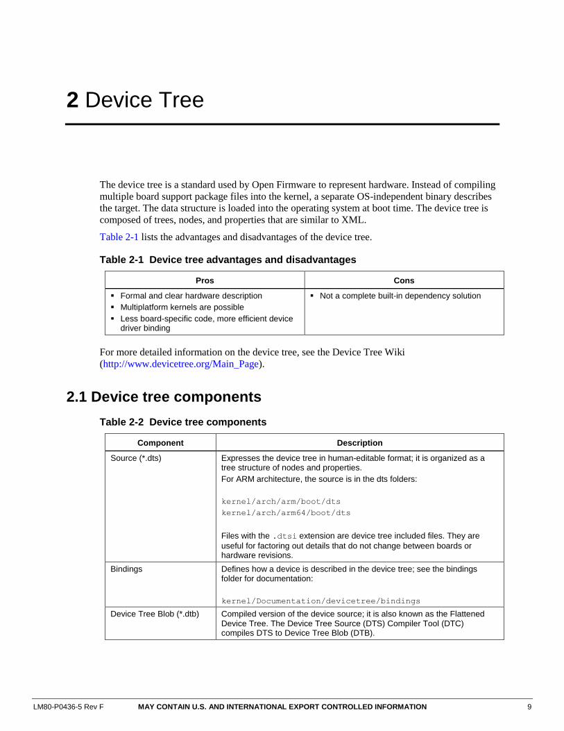
Table 2-1 lists the advantages and disadvantages of the device tree.
Table 2-1 Device tree advantages and disadvantages
Pros Cons
Formal and clear hardware description
Multiplatform kernels are possible
Less board-specific code, more efficient device driver binding
Not a complete built-in dependency solution
For more detailed information on the device tree, see the Device Tree Wiki
(http://www.devicetree.org/Main_Page).
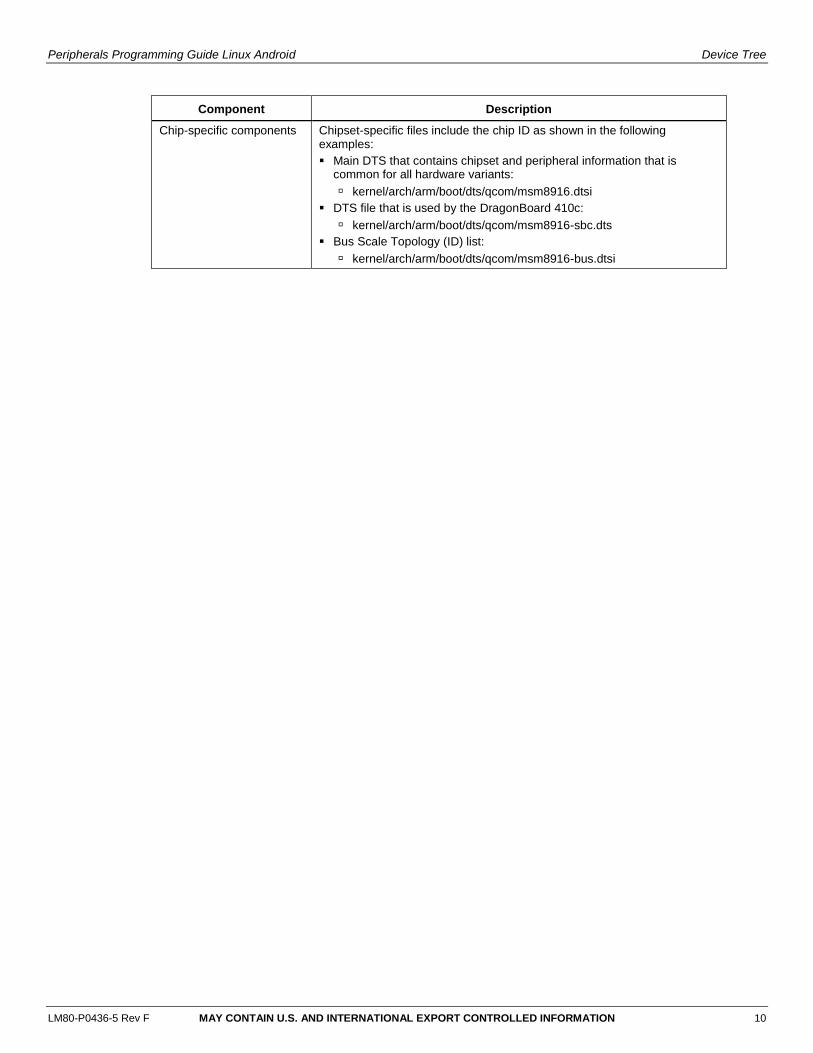
2.1 Device tree components
Table 2-2 Device tree components
Component Description
Source (*.dts) Expresses the device tree in human-editable format; it is organized as a tree structure of nodes and properties.
For ARM architecture, the source is in the dts folders:
kernel/arch/arm/boot/dts
kernel/arch/arm64/boot/dts
Files with the .dtsi extension are device tree included files. They are
useful for factoring out details that do not change between boards or hardware revisions.
Bindings Defines how a device is described in the device tree; see the bindings folder for documentation:
kernel/Documentation/devicetree/bindings
Device Tree Blob (*.dtb) Compiled version of the device source; it is also known as the Flattened Device Tree. The Device Tree Source (DTS) Compiler Tool (DTC) compiles DTS to Device Tree Blob (DTB).
Peripherals Programming Guide Linux Android Device Tree
LM80-P0436-5 Rev F MAY CONTAIN U.S. AND INTERNATIONAL EXPORT CONTROLLED INFORMATION 10
Component Description
Chip-specific components Chipset-specific files include the chip ID as shown in the following examples:
Main DTS that contains chipset and peripheral information that is common for all hardware variants:
kernel/arch/arm/boot/dts/qcom/msm8916.dtsi
DTS file that is used by the DragonBoard 410c:
kernel/arch/arm/boot/dts/qcom/msm8916-sbc.dts
Bus Scale Topology (ID) list:
kernel/arch/arm/boot/dts/qcom/msm8916-bus.dtsi
LM80-P0436-5 Rev F MAY CONTAIN U.S. AND INTERNATIONAL EXPORT CONTROLLED INFORMATION 11
3 Universal Asynchronous Receiver/ Transmitter
This chapter describes the Universal Asynchronous Receiver/Transmitter (UART) and explains
how to configure it in the boot loader and kernel.
3.1 Hardware overview
3.1.1 BLSP
APQ8016E supports many peripherals via the generic serial bus interface supported by the BAM
Low Speed Peripherals (BLSP) core. It has single BLSP instance which supports up to six serial
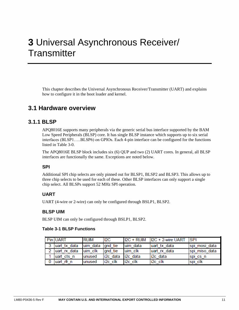
interfaces (BLSP1…..BLSP6) on GPIOs. Each 4-pin interface can be configured for the functions
listed in Table 3-0.
The APQ8016E BLSP block includes six (6) QUP and two (2) UART cores. In general, all BLSP
interfaces are functionally the same. Exceptions are noted below.
SPI
Additional SPI chip selects are only pinned out for BLSP1, BLSP2 and BLSP3. This allows up to
three chip selects to be used for each of these. Other BLSP interfaces can only support a single
chip select. All BLSPs support 52 MHz SPI operation.
UART
UART (4-wire or 2-wire) can only be configured through BSLP1, BLSP2.
BLSP UIM
BLSP UIM can only be configured through BSLP1, BLSP2.
Table 3-1 BLSP Functions
DragonBoard™ 410c based on Qualcomm® Snapdragon™ 410E processor Peripherals Programming Guide Linux Android Universal Asynchronous Receiver/ Transmitter
LM80-P0436-5 Rev F MAY CONTAIN U.S. AND INTERNATIONAL EXPORT CONTROLLED INFORMATION 12
The Qualcomm Universal Peripheral (QUP) Serial Engine provides a general purpose datapath
engine to support multiple mini cores. Each mini core implements protocol-specific logic. The
common FIFO provides a consistent system IO buffer and system DMA model across widely
varying external interface types. For example, one pair of FIFO buffers can support Serial
Peripheral Interface (SPI) and I2C mini cores independently.
BAM is used as a hardware data mover. Each BLSP peripheral:
Is statically connected to a pair of BAM pipes
Consists of 12 pipes that can be used for data move operations for APQ8016E
Supports BAM- and non-BAM-based data transfers
3.1.2 UART core
Key features added for the chipset include the following:
BAM support
Single-character mode
Baudrates 300 bps up to 4M bps
Detail information in msm_hsl_set_baud_rate() of
kernel/drivers/tty/serial/msm_serial_hs_lite.c
Detail information in msm_hs_set_bps_locked() of kernel/drivers/tty/serial/msm_serial_hs.c
The UART core is used for transmitting and receiving data through a serial interface. It is used
for communicating with other UART protocol devices. Configuration of this mode is primarily
defined by the UART_DM_MR1 and UART_DM_MR2 registers (Snapdragon 410E
(APQ8016E) Hardware Register Description document has the register information -
https://developer.qualcomm.com/hardware/snapdragon-410/tools).
To match the labeling in the software interface manual, each UART is identified by the BLSP
core and UART core (0 to 5). The max transfer rate of the UART core is up to 4M bps.
Peripherals Programming Guide Linux Android Universal Asynchronous Receiver/ Transmitter
LM80-P0436-5 Rev F MAY CONTAIN U.S. AND INTERNATIONAL EXPORT CONTROLLED INFORMATION 13
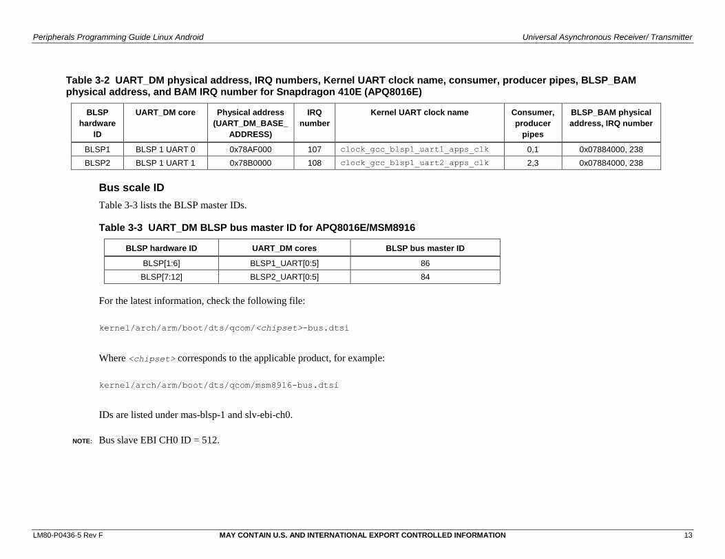
Table 3-2 UART_DM physical address, IRQ numbers, Kernel UART clock name, consumer, producer pipes, BLSP_BAM physical address, and BAM IRQ number for Snapdragon 410E (APQ8016E)
BLSP
hardware
ID
UART_DM core Physical address
(UART_DM_BASE_
ADDRESS)
IRQ
number
Kernel UART clock name Consumer,
producer
pipes
BLSP_BAM physical
address, IRQ number
BLSP1 BLSP 1 UART 0 0x78AF000 107 clock_gcc_blsp1_uart1_apps_clk 0,1 0x07884000, 238
BLSP2 BLSP 1 UART 1 0x78B0000 108 clock_gcc_blsp1_uart2_apps_clk 2,3 0x07884000, 238
Bus scale ID
Table 3-3 lists the BLSP master IDs.
Table 3-3 UART_DM BLSP bus master ID for APQ8016E/MSM8916
BLSP hardware ID UART_DM cores BLSP bus master ID
BLSP[1:6] BLSP1_UART[0:5] 86
BLSP[7:12] BLSP2_UART[0:5] 84
For the latest information, check the following file:
kernel/arch/arm/boot/dts/qcom/<chipset>-bus.dtsi
Where <chipset> corresponds to the applicable product, for example:
kernel/arch/arm/boot/dts/qcom/msm8916-bus.dtsi
IDs are listed under mas-blsp-1 and slv-ebi-ch0.
NOTE: Bus slave EBI CH0 ID = 512.
Peripherals Programming Guide Linux Android Universal Asynchronous Receiver/ Transmitter
LM80-P0436-5 Rev F MAY CONTAIN U.S. AND INTERNATIONAL EXPORT CONTROLLED INFORMATION 14
3.2 Configure LK UART
In the Little Kernel (LK) boot loader, a UART may be needed for debug logs.
3.2.1 Code changes
This section describes the changes required to configure a UART in the LK boot loader. The
following files are used to configure UART in the boot loader:
/bootable/bootloader/lk/project/<chipset>.mk
/bootable/bootloader/lk/target/<chipset>/init.c
/bootable/bootloader/lk/platform/<chipset>/include/platform/iomap.h
/bootable/bootloader/lk/platform/<chipset>/acpuclock.c
/bootable/bootloader/lk/platform/<chipset>/<chipset>-clock.c
/bootable/bootloader/lk/platform/<chipset>/gpio.c
kernel/arch/arm/mach-msm/include/mach/msm_iomap-<chip>.h
Where <chipset> corresponds to the applicable chipset, and <chip> corresponds to the 4-digit
chip number, for example:
/bootable/bootloader/lk/project/msm8916.mk
kernel/arch/arm/mach-msm/include/mach/msm_iomap-8916.h
1. Enable the UART for debugging.
a. Open the project make file.
Project_Root/bootable/bootloader/lk/project/<chipset>.mk
Where <chipset> corresponds to the applicable chipset, for example:
Project_Root/bootable/bootloader/lk/project/msms8916.mk
b. Set the WITH_DEBUG_UART flag to TRUE.
DEFINES += WITH_DEBUG_UART=1
2. Set the base address.
a. Open the init.c file located at:
Project_Root/bootable/bootloader/lk/target/<chipset>/init.c
Where <chipset> corresponds to the applicable chipset, for example:
Project_Root/bootable/bootloader/lk/target/msm8916/init.c
Peripherals Programming Guide Linux Android Universal Asynchronous Receiver/ Transmitter
LM80-P0436-5 Rev F MAY CONTAIN U.S. AND INTERNATIONAL EXPORT CONTROLLED INFORMATION 15
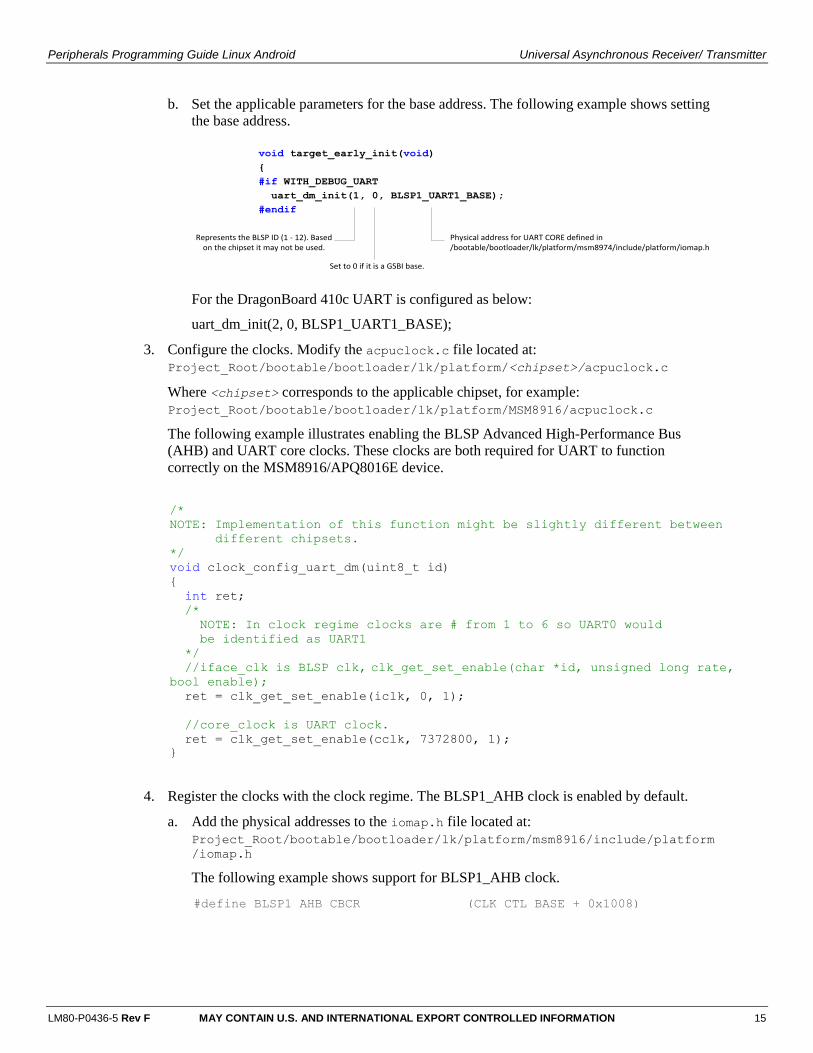
b. Set the applicable parameters for the base address. The following example shows setting
the base address.
void target_early_init(void)
{
#if WITH_DEBUG_UART
uart_dm_init(1, 0, BLSP1_UART1_BASE);
#endif
Represents the BLSP ID (1 - 12). Based on the chipset it may not be used.
Set to 0 if it is a GSBI base.
Physical address for UART CORE defined in /bootable/bootloader/lk/platform/msm8974/include/platform/iomap.h
For the DragonBoard 410c UART is configured as below:
uart_dm_init(2, 0, BLSP1_UART1_BASE);
3. Configure the clocks. Modify the acpuclock.c file located at:
Project_Root/bootable/bootloader/lk/platform/<chipset>/acpuclock.c
Where <chipset> corresponds to the applicable chipset, for example:
Project_Root/bootable/bootloader/lk/platform/MSM8916/acpuclock.c
The following example illustrates enabling the BLSP Advanced High-Performance Bus
(AHB) and UART core clocks. These clocks are both required for UART to function
correctly on the MSM8916/APQ8016E device.
4. Register the clocks with the clock regime. The BLSP1_AHB clock is enabled by default.
a. Add the physical addresses to the iomap.h file located at:
Project_Root/bootable/bootloader/lk/platform/msm8916/include/platform
/iomap.h
The following example shows support for BLSP1_AHB clock.
/*
NOTE: Implementation of this function might be slightly different between
different chipsets.
*/
void clock_config_uart_dm(uint8_t id)
{
int ret;
/*
NOTE: In clock regime clocks are # from 1 to 6 so UART0 would
be identified as UART1
*/
//iface_clk is BLSP clk, clk_get_set_enable(char *id, unsigned long rate, bool enable);
ret = clk_get_set_enable(iclk, 0, 1);
//core_clock is UART clock.
ret = clk_get_set_enable(cclk, 7372800, 1);
}
#define BLSP1_AHB_CBCR (CLK_CTL_BASE + 0x1008)
Peripherals Programming Guide Linux Android Universal Asynchronous Receiver/ Transmitter
LM80-P0436-5 Rev F MAY CONTAIN U.S. AND INTERNATIONAL EXPORT CONTROLLED INFORMATION 16
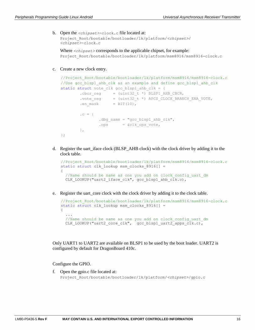
b. Open the <chipset>-clock.c file located at:
Project_Root/bootable/bootloader/lk/platform/<chipset>/
<chipset>-clock.c
Where <chipset> corresponds to the applicable chipset, for example:
Project_Root/bootable/bootloader/lk/platform/msm8916/msm8916-clock.c
c. Create a new clock entry.
d. Register the uart_iface clock (BLSP_AHB clock) with the clock driver by adding it to the
clock table.
e. Register the uart_core clock with the clock driver by adding it to the clock table.
Only UART1 to UART2 are available on BLSP1 to be used by the boot loader. UART2 is
configured by default for DragonBoard 410c.
Configure the GPIO.
f. Open the gpio.c file located at:
Project_Root/bootable/bootloader/lk/platform/<chipset>/gpio.c
//Project_Root/bootable/bootloader/lk/platform/msm8916/msm8916-clock.c
//Use gcc_blsp1_ahb_clk as an example and define gcc_blsp1_ahb_clk
static struct vote_clk gcc_blsp1_ahb_clk = {
.cbcr_reg = (uint32_t *) BLSP1_AHB_CBCR,
.vote_reg = (uint32_t *) APCS_CLOCK_BRANCH_ENA_VOTE,
.en_mask = BIT(10),
.c = {
.dbg_name = "gcc_blsp1_ahb_clk",
.ops = &clk_ops_vote,
},
};
//Project_Root/bootable/bootloader/lk/platform/msm8916/msm8916-clock.c
static struct clk_lookup msm_clocks_8916[] =
{
//Name should be same as one you add on clock_config_uart_dm
CLK_LOOKUP("uart2_iface_clk", gcc_blsp1_ahb_clk.c),
//Project_Root/bootable/bootloader/lk/platform/msm8916/msm8916-clock.c
static struct clk_lookup msm_clocks_8916[] =
{
...
//Name should be same as one you add on clock_config_uart_dm
CLK_LOOKUP("uart2_core_clk", gcc_blsp1_uart2_apps_clk.c),
Peripherals Programming Guide Linux Android Universal Asynchronous Receiver/ Transmitter
LM80-P0436-5 Rev F MAY CONTAIN U.S. AND INTERNATIONAL EXPORT CONTROLLED INFORMATION 17
g. Configure the correct GPIO.
NOTE: See the device pinout for information about the GPIO function. BLSPs 4, 5, 6, 7, 9, and 11 have
different function assignments compared to other BLSPs.
5. Configure Early Printk
Additional changes are needed during kernel configuration if the following features are
enabled in the kernel/arch/arm/configs/<chipset>_defconfig file:
CONFIG_DEBUG_LL=y
CONFIG_EARLY_PRINTK=y
There is a dependency between UART configuration on the little kernel and the Early Printk
driver in the kernel. If the configuration settings listed above are enabled, the following
message is displayed using the Early Printk driver:
"Uncompressing Linux..."
The message output is defined in the Early Printk driver.
void gpio_config_uart_dm(uint8_t id)
{
/*
Configure the RX/TX GPIO
Argument 1: GPIO #
Argument 2: Function (Please see device pinout for more information)
Argument 3: Input/Output (Can be 0/1)
Argument 4: Should be no PULL
Argument 5: Drive strength
Argument 6: Output Enable (Can be 0/1)
*/
gpio_tlmm_config(5, 2, GPIO_INPUT, GPIO_NO_PULL,
GPIO_8MA, GPIO_DISABLE);
gpio_tlmm_config(4, 2, GPIO_OUTPUT, GPIO_NO_PULL,
GPIO_8MA, GPIO_DISABLE);
}
void
decompress_kernel(unsigned long output_start, unsigned long free_mem_ptr_p,
unsigned long free_mem_ptr_end_p,
int arch_id)
{
int ret;
...
arch_decomp_setup();
putstr("Uncompressing Linux..."); //uses early printk driver
ret = do_decompress(input_data, input_data_end - input_data,
...
}
Peripherals Programming Guide Linux Android Universal Asynchronous Receiver/ Transmitter
LM80-P0436-5 Rev F MAY CONTAIN U.S. AND INTERNATIONAL EXPORT CONTROLLED INFORMATION 18
a. The Early Printk driver depends on the little kernel to configure the UART port. Open the
msm_iomap-8916.h file located at:
Project_Root kernel/arch/arm/mach-msm/include/mach/msm_iomap-<chip>.h
Where <chip> corresponds to the 4-digit chip number, for example:
Project_Root kernel/arch/arm/mach-msm/include/mach/msm_iomap-8916.h
b. Ensure the UART port being configured in the little kernel is the same UART port that is
used by the kernel.
3.2.2 Debug LK UART
If the UART is properly configured, the following message appears on the serial console:
Android Bootloader - UART_DM Initialized!!!
If you do not see the message, verify that the GPIOs are correctly configured. Check the GPIO
configuration register, GPIO_CFGn, to ensure that the GPIO settings are valid.
Physical Address: 0x01000000 + (0x1000 * n) = GPIO_CFGn
n = GPIO #
Example Address:
0x01000000 = GPIO_CFG0
0x01001000 = GPIO_CFG1
Bit definition for GPIO_CFGn
Bits 31:11 Reserved
Bit 10 GPIO_HIHYS_EN Control the hihys_EN for GPIO
Bit 9 GPIO_OE Controls the Output Enable for GPIO
when in GPIO mode.
Bits 8:6 DRV_STRENGTH Control Drive Strength
000:2mA 001:4mA 010:6mA 011:8mA
100:10mA 101:12mA 110:14mA 111:16mA
Bits 5:2 FUNC_SEL Make sure Function is GSBI
Check Device Pinout for Correct Function
Bits 1:0 GPIO_PULL Internal Pull Configuration
00:No Pull 01: Pull Down
10:Keeper 11: Pull Up
NOTE: For UART, 8 mA with no pull is recommended.
#ifdef CONFIG_DEBUG_MSM8916_UART
#define MSM_DEBUG_UART_BASE IOMEM(0xFA0B0000)
#define MSM_DEBUG_UART_PHYS 0x78B0000
#endif
Peripherals Programming Guide Linux Android Universal Asynchronous Receiver/ Transmitter
LM80-P0436-5 Rev F MAY CONTAIN U.S. AND INTERNATIONAL EXPORT CONTROLLED INFORMATION 19
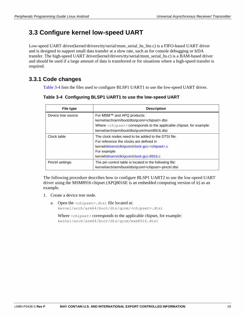
3.3 Configure kernel low-speed UART
Low-speed UART driver(kernel/drivers/tty/serial/msm_serial_hs_lite.c) is a FIFO-based UART driver
and is designed to support small data transfer at a slow rate, such as for console debugging or IrDA
transfer. The high-speed UART driver(kernel/drivers/tty/serial/msm_serial_hs.c) is a BAM-based driver
and should be used if a large amount of data is transferred or for situations where a high-speed transfer is
required.
3.3.1 Code changes
Table 3-4 lists the files used to configure BLSP1 UART1 to use the low-speed UART driver.
Table 3-4 Configuring BLSP1 UART1 to use the low-speed UART
File type Description
Device tree source For MSM™ and APQ products:
kernel/arch/arm/boot/dts/qcom/<chipset>.dtsi
Where <chipset> corresponds to the applicable chipset, for example:
kernel/arch/arm/boot/dts/qcom/msm8916.dtsi
Clock table The clock nodes need to be added to the DTSI file.
For reference the clocks are defined in
kernel/drivers/clk/qcom/clock-gcc-<chipset>.c
For example
kernel/drivers/clk/qcom/clock-gcc-8916.c
Pinctrl settings The pin control table is located in the following file:
kernel/arch/arm/boot/dts/qcom/<chipset>-pinctrl.dtsi
The following procedure describes how to configure BLSP1 UART2 to use the low-speed UART
driver using the MSM8916 chipset (APQ8016E is an embedded computing version of it) as an
example.
1. Create a device tree node.
a. Open the <chipset>.dtsi file located at:
kernel/arch/arm64/boot/dts/qcom/<chipset>.dtsi
Where <chipset> corresponds to the applicable chipset, for example:
kernel/arch/arm64/boot/dts/qcom/msm8916.dtsi
Peripherals Programming Guide Linux Android Universal Asynchronous Receiver/ Transmitter
LM80-P0436-5 Rev F MAY CONTAIN U.S. AND INTERNATIONAL EXPORT CONTROLLED INFORMATION 20
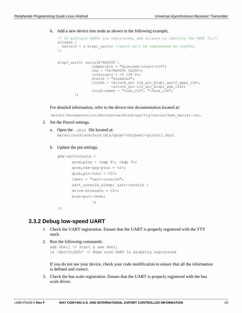
b. Add a new device tree node as shown in the following example.
For detailed information, refer to the device tree documentation located at:
kernel/Documentation/devicetree/bindings/tty/serial/msm_serial.txt.
2. Set the Pinctrl settings.
a. Open the .dtsi file located at:
kernel/arch/arm/boot/dts/qcom/<chipset>-pinctrl.dtsi
b. Update the pin settings.
3.3.2 Debug low-speed UART
1. Check the UART registration. Ensure that the UART is properly registered with the TTY
stack.
2. Run the following commands:
adb shell -> start a new shell
ls /dev/ttyHSL* -> Make sure UART is properly registered
If you do not see your device, check your code modification to ensure that all the information
is defined and correct.
3. Check the bus scale registration. Ensure that the UART is properly registered with the bus
scale driver.
/* If multiple UARTs are registered, add aliases to identify the UART ID.*/
aliases {
serial2 = & blsp1_uart2; //uart2 will be registered as ttyHSL2
};
blsp1_uart2: serial@78b0000 {
compatible = "qcom,msm-lsuart-v14";
reg = <0x78b0000 0x200>;
interrupts = <0 108 0>;
status = "disabled";
clocks = <&clock_gcc clk_gcc_blsp1_uart2_apps_clk>,
<&clock_gcc clk_gcc_blsp1_ahb_clk>;
clock-names = "core_clk", "iface_clk";
};
pmx-uartconsole {
qcom,pins = <&gp 4>, <&gp 5>;
qcom,num-grp-pins = <2>;
qcom,pin-func = <2>;
label = "uart-console";
uart_console_sleep: uart-console {
drive-strength = <2>;
bias-pull-down;
};
};
Peripherals Programming Guide Linux Android Universal Asynchronous Receiver/ Transmitter
LM80-P0436-5 Rev F MAY CONTAIN U.S. AND INTERNATIONAL EXPORT CONTROLLED INFORMATION 21
a. Run the following commands:
adb shell
mount -t debugfs none /sys/kernel/debug -> mount debug fs
cat /dev/ttyHSL# -> Open the UART port
b. Go to the bus scale directory.
cd /sys/kernel/debug/msm-bus-dbg/client-data
ls
c. Confirm that the name that was put on msm-bus is there, for example, blsp1_uart1.
d. Cat client_name, for example:
cat blsp1_uart1
Output: Confirm curr = 1, and rest of values.
curr : 1
masters: 86
slaves : 512
ab : 500000
ib : 800000
If you do not see your device, check your code modification to ensure that all of the
information is defined and correct.
4. Check the internal loopback. Run the following commands to enable loopback:
adb shell
mount -t debugfs none /sys/kernel/debug -> mount debug fs
cd /sys/kernel/debug/msm_serial_hsl -> directory for Low Speed UART
echo 1 > loopback.# -> enable loopback. # = device #
cat loopback.# -> make sure returns 1
5. Open another shell to dump the UART Rx data.
adb shell
cat /dev/ttyHSL# ->Dump any data UART Receive
6. Transmit some test data through a separate shell.
adb shell
echo "This Document Is Very Much Helpful" > /dev/ttyHSL# ->Transfer data
If the loopback works:
– Test message loop appears continuously in the command shell until you exit the cat
program. This is because of the internal loopback and how the cat program opens the
UART.
– It is safe to assume that the UART is properly configured and only the GPIO settings
must be confirmed.
If loopback does not work:
i Ensure that the UART is still in the Active state. Open the UART from the shell:
Peripherals Programming Guide Linux Android Universal Asynchronous Receiver/ Transmitter
LM80-P0436-5 Rev F MAY CONTAIN U.S. AND INTERNATIONAL EXPORT CONTROLLED INFORMATION 22
adb shell
cat /dev/ttyHSL# ->Dump any data UART Receive
ii Check the clock settings.
iii Measure the clocks from the debug-fs command.
Make sure the Peripheral Network on a Chip (PNoC) clock is running.
cat /sys/kernel/debug/clk/pcnoc_clk/measure
Measure the BLSP AHB clock.
label: gcc_blsp1:2_ahb_clk
For example, cat /sys/kernel/debug/clk/gcc_blsp1_ahb_clk/measure
Measure the UART core clock.
label: gcc_blsp1:2_uart1:6_apps_clk
For example, cat /sys/kernel/debug/clk/gcc_blsp1_uart2_apps_ clk/measure
Loopback works, but there is no signal output to check the GPIO settings. For
instructions, see Section 3.2.2.
3.3.3 Optional configuration changes
After basic UART functionality is verified, enhance UART_DM functionality by configuring
runtime GPIO and preventing system suspend.
3.3.3.1 Prevent system suspend
If required when the UART is in operation, the UART driver can prevent system suspend by
automatically holding a wakelock.
1. Update the device tree. Open the device tree file located at:
kernel/arch/arm/boot/dts/qcom/<chipset>-sbc.dtsi
2. Add the use-pm node.
3. Confirm that the UART driver is holding the wakelock.
a. Open the UART port.
adb shell
//Add following additional nodes to enable wakelock
BLSP1_UART1
qcom,use-pm; //Whenever port open wakelock will be held
Peripherals Programming Guide Linux Android Universal Asynchronous Receiver/ Transmitter
LM80-P0436-5 Rev F MAY CONTAIN U.S. AND INTERNATIONAL EXPORT CONTROLLED INFORMATION 23
cat /dev/ttyHSL#
b. Dump the wake-up sources.
cat /sys/kernel/debug/wakeup_sources
msm_serial_hslite_port_open 2 2 0 0 1430 - Confirm
active_since != 0
4. Close the UART port. Confirm that active_since returns to zero.
For more information, see
kernel/Documentation/devicetree/bindings/tty/serial/msm_serial.txt.
3.4 Configure kernel high-speed UART
UART_DM can be configured as a BAM-based UART. This driver is designed for high-speed,
large data transfers, such as Bluetooth communication.
The following procedure describes how to configure BLSP1_UART1 as a high-speed UART.
1. Create a device tree node.
a. Open the device tree file located at:
kernel/arch/arm/boot/dts/qcom/msm8916.dtsi
Peripherals Programming Guide Linux Android Universal Asynchronous Receiver/ Transmitter
LM80-P0436-5 Rev F MAY CONTAIN U.S. AND INTERNATIONAL EXPORT CONTROLLED INFORMATION 24
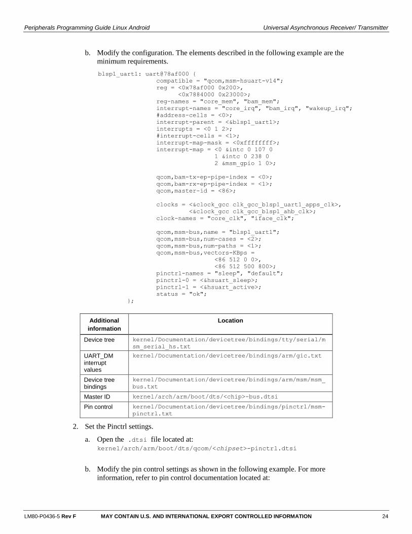
b. Modify the configuration. The elements described in the following example are the
minimum requirements.
Additional
information
Location
Device tree kernel/Documentation/devicetree/bindings/tty/serial/m
sm_serial_hs.txt
UART_DM interrupt values
kernel/Documentation/devicetree/bindings/arm/gic.txt
Device tree bindings
kernel/Documentation/devicetree/bindings/arm/msm/msm_
bus.txt
Master ID kernel/arch/arm/boot/dts/<chip>-bus.dtsi
Pin control kernel/Documentation/devicetree/bindings/pinctrl/msm-
pinctrl.txt
2. Set the Pinctrl settings.
a. Open the .dtsi file located at:
kernel/arch/arm/boot/dts/qcom/<chipset>-pinctrl.dtsi
b. Modify the pin control settings as shown in the following example. For more
information, refer to pin control documentation located at:
blsp1_uart1: uart@78af000 {
compatible = "qcom,msm-hsuart-v14";
reg = <0x78af000 0x200>,
<0x7884000 0x23000>;
reg-names = "core_mem", "bam_mem";
interrupt-names = "core_irq", "bam_irq", "wakeup_irq";
#address-cells = <0>;
interrupt-parent = <&blsp1_uart1>;
interrupts = <0 1 2>;
#interrupt-cells = <1>;
interrupt-map-mask = <0xffffffff>;
interrupt-map = <0 &intc 0 107 0
1 &intc 0 238 0
2 &msm_gpio 1 0>;
qcom,bam-tx-ep-pipe-index = <0>;
qcom,bam-rx-ep-pipe-index = <1>;
qcom,master-id = <86>;
clocks = <&clock_gcc clk_gcc_blsp1_uart1_apps_clk>,
<&clock_gcc clk_gcc_blsp1_ahb_clk>;
clock-names = "core_clk", "iface_clk";
qcom,msm-bus,name = "blsp1_uart1";
qcom,msm-bus,num-cases = <2>;
qcom,msm-bus,num-paths = <1>;
qcom,msm-bus,vectors-KBps =
<86 512 0 0>,
<86 512 500 800>;
pinctrl-names = "sleep", "default";
pinctrl-0 = <&hsuart_sleep>;
pinctrl-1 = <&hsuart_active>;
status = "ok";
};
Peripherals Programming Guide Linux Android Universal Asynchronous Receiver/ Transmitter
LM80-P0436-5 Rev F MAY CONTAIN U.S. AND INTERNATIONAL EXPORT CONTROLLED INFORMATION 25
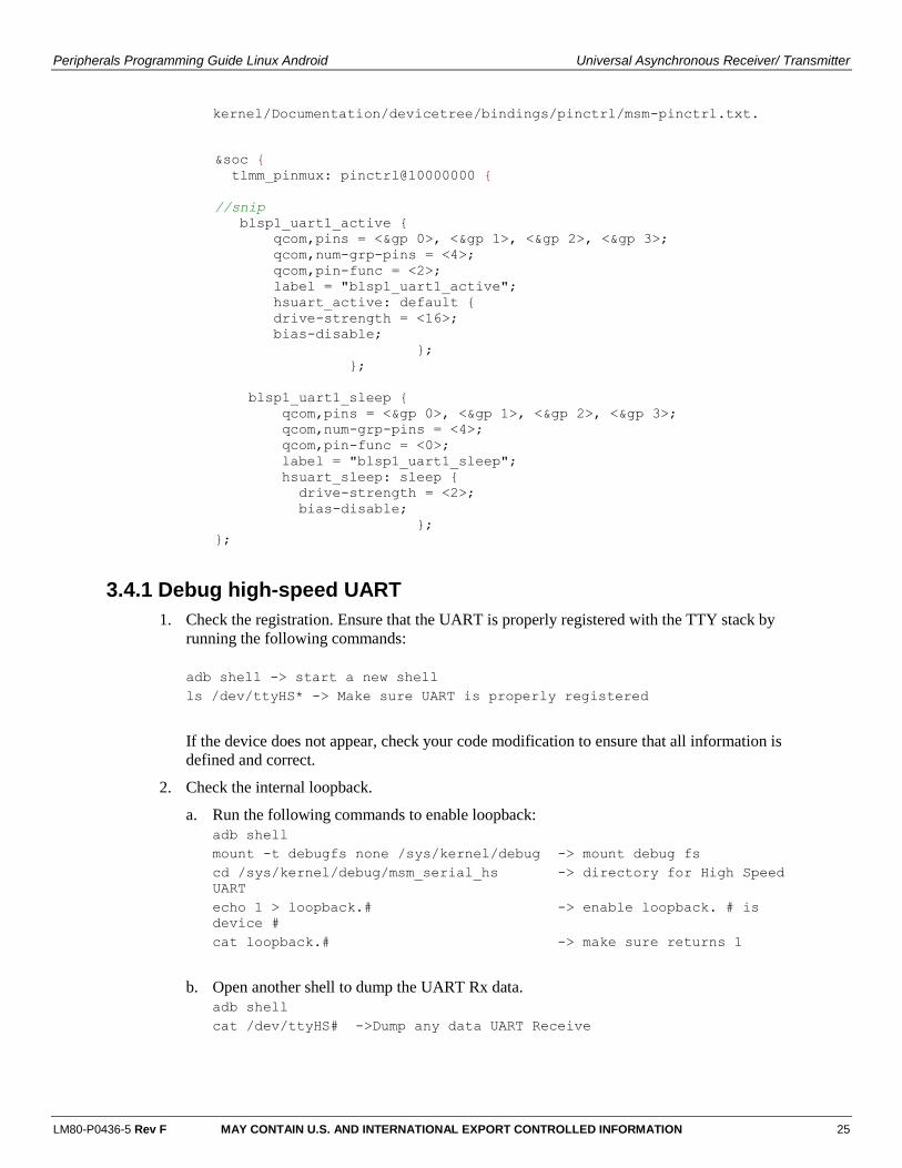
kernel/Documentation/devicetree/bindings/pinctrl/msm-pinctrl.txt.
3.4.1 Debug high-speed UART
1. Check the registration. Ensure that the UART is properly registered with the TTY stack by
running the following commands:
adb shell -> start a new shell
ls /dev/ttyHS* -> Make sure UART is properly registered
If the device does not appear, check your code modification to ensure that all information is
defined and correct.
2. Check the internal loopback.
a. Run the following commands to enable loopback:
adb shell
mount -t debugfs none /sys/kernel/debug -> mount debug fs
cd /sys/kernel/debug/msm_serial_hs -> directory for High Speed
UART
echo 1 > loopback.# -> enable loopback. # is
device #
cat loopback.# -> make sure returns 1
b. Open another shell to dump the UART Rx data.
adb shell
cat /dev/ttyHS# ->Dump any data UART Receive
&soc {
tlmm_pinmux: pinctrl@10000000 {
//snip
blsp1_uart1_active {
qcom,pins = <&gp 0>, <&gp 1>, <&gp 2>, <&gp 3>;
qcom,num-grp-pins = <4>;
qcom,pin-func = <2>;
label = "blsp1_uart1_active";
hsuart_active: default {
drive-strength = <16>;
bias-disable;
};
};
blsp1_uart1_sleep {
qcom,pins = <&gp 0>, <&gp 1>, <&gp 2>, <&gp 3>;
qcom,num-grp-pins = <4>;
qcom,pin-func = <0>;
label = "blsp1_uart1_sleep";
hsuart_sleep: sleep {
drive-strength = <2>;
bias-disable;
};
};
Peripherals Programming Guide Linux Android Universal Asynchronous Receiver/ Transmitter
LM80-P0436-5 Rev F MAY CONTAIN U.S. AND INTERNATIONAL EXPORT CONTROLLED INFORMATION 26
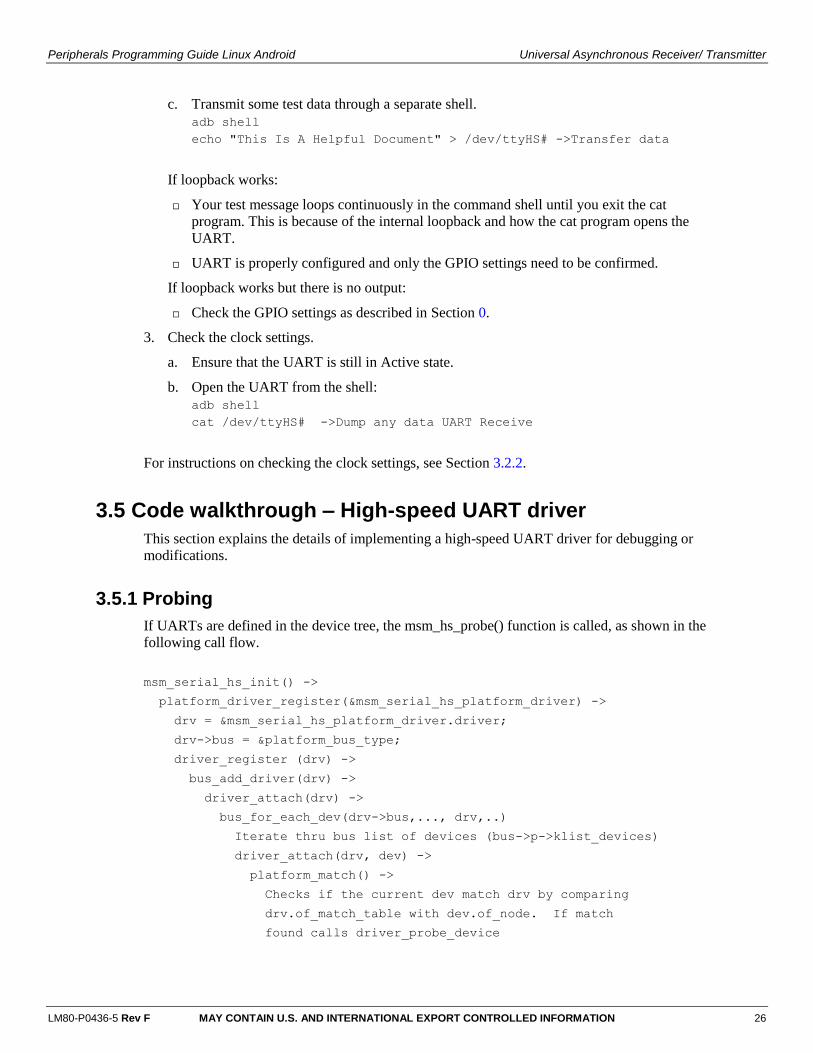
c. Transmit some test data through a separate shell.
adb shell
echo "This Is A Helpful Document" > /dev/ttyHS# ->Transfer data
If loopback works:
Your test message loops continuously in the command shell until you exit the cat
program. This is because of the internal loopback and how the cat program opens the
UART.
UART is properly configured and only the GPIO settings need to be confirmed.
If loopback works but there is no output:
Check the GPIO settings as described in Section 0.
3. Check the clock settings.
a. Ensure that the UART is still in Active state.
b. Open the UART from the shell:
adb shell
cat /dev/ttyHS# ->Dump any data UART Receive
For instructions on checking the clock settings, see Section 3.2.2.
3.5 Code walkthrough – High-speed UART driver
This section explains the details of implementing a high-speed UART driver for debugging or
modifications.
3.5.1 Probing
If UARTs are defined in the device tree, the msm_hs_probe() function is called, as shown in the
following call flow.
msm_serial_hs_init() ->
platform_driver_register(&msm_serial_hs_platform_driver) ->
drv = &msm_serial_hs_platform_driver.driver;
drv->bus = &platform_bus_type;
driver_register (drv) ->
bus_add_driver(drv) ->
driver_attach(drv) ->
bus_for_each_dev(drv->bus,..., drv,..)
Iterate thru bus list of devices (bus->p->klist_devices)
driver_attach(drv, dev) ->
platform_match() ->
Checks if the current dev match drv by comparing
drv.of_match_table with dev.of_node. If match
found calls driver_probe_device
Peripherals Programming Guide Linux Android Universal Asynchronous Receiver/ Transmitter
LM80-P0436-5 Rev F MAY CONTAIN U.S. AND INTERNATIONAL EXPORT CONTROLLED INFORMATION 27
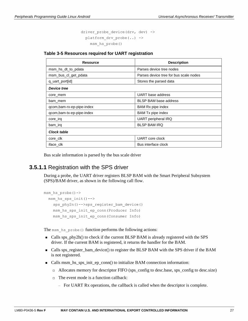
driver_probe_device(drv, dev) ->
platform_drv_probe(..) ->
msm_hs_probe()
Table 3-5 Resources required for UART registration
Resource Description
msm_hs_dt_to_pdata Parses device tree nodes
msm_bus_cl_get_pdata Parses device tree for bus scale nodes
q_uart_port[id] Stores the parsed data
Device tree
core_mem UART base address
bam_mem BLSP BAM base address
qcom,bam-rx-ep-pipe-index BAM Rx pipe index
qcom,bam-tx-ep-pipe-index BAM Tx pipe index
core_irq UART peripheral IRQ
bam_irq BLSP BAM IRQ
Clock table
core_clk UART core clock
iface_clk Bus interface clock
Bus scale information is parsed by the bus scale driver
3.5.1.1 Registration with the SPS driver
During a probe, the UART driver registers BLSP BAM with the Smart Peripheral Subsystem
(SPS)/BAM driver, as shown in the following call flow.
msm_hs_probe()->
msm_hs_sps_init()-->
sps_phy2n()-->sps_register_bam_device()
msm_hs_sps_init_ep_conn(Producer Info)
msm_hs_sps_init_ep_conn(Consumer Info)
The msm_hs_probe() function performs the following actions:
Calls sps_phy2h() to check if the current BLSP BAM is already registered with the SPS
driver. If the current BAM is registered, it returns the handler for the BAM.
Calls sps_register_bam_device() to register the BLSP BAM with the SPS driver if the BAM
is not registered.
Calls msm_hs_sps_init_ep_conn() to initialize BAM connection information:
Allocates memory for descriptor FIFO (sps_config to desc.base, sps_config to desc.size)
The event mode is a function callback:
– For UART Rx operations, the callback is called when the descriptor is complete.
Peripherals Programming Guide Linux Android Universal Asynchronous Receiver/ Transmitter
LM80-P0436-5 Rev F MAY CONTAIN U.S. AND INTERNATIONAL EXPORT CONTROLLED INFORMATION 28
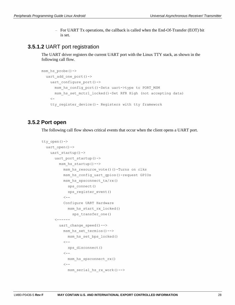
– For UART Tx operations, the callback is called when the End-Of-Transfer (EOT) bit
is set.
3.5.1.2 UART port registration
The UART driver registers the current UART port with the Linux TTY stack, as shown in the
following call flow.
msm_hs_probe()->
uart_add_one_port()->
uart_configure_port()->
msm_hs_config_port()-Sets uart->type to PORT_MSM
msm_hs_set_mctrl_locked()-Set RFR High (not accepting data)
<-
tty_register_device()- Registers with tty framework
3.5.2 Port open
The following call flow shows critical events that occur when the client opens a UART port.
tty_open()->
uart_open()->
uart_startup()->
uart_port_startup()->
msm_hs_startup()-->
msm_hs_resource_vote()()-Turns on clks
msm_hs_config_uart_gpios()-request GPIOs
msm_hs_spsconnect_tx/rx()
sps_connect()
sps_register_event()
<--
Configure UART Hardware
msm_hs_start_rx_locked()
sps_transfer_one()
<------
uart_change_speed()-->
msm_hs_set_termios()-->
msm_hs_set_bps_locked()
<--
sps_disconnect()
<--
msm_hs_spsconnect_rx()
<--
msm_serial_hs_rx_work()-->
Peripherals Programming Guide Linux Android Universal Asynchronous Receiver/ Transmitter
LM80-P0436-5 Rev F MAY CONTAIN U.S. AND INTERNATIONAL EXPORT CONTROLLED INFORMATION 29
msm_hs_start_rx_locked()
<--------------
The uart_open() function performs the following actions:
Increments port->count.
If a port is not initialized (port->flags and ASYNC_INITIALIZED):
Allocates and clears a Tx buffer (uart_state->xmit.buf)
Calls msm_hs_startup()
The msm_hs_startup() function initializes the low-level UART core:
Maps the Tx buffer to be a Direct Memory Access (DMA) capable buffer.
Turns on all necessary clocks, including the bus scale request.
If runtime GPIO configuration is enabled, requests the GPIOs (see Section 3.3.3).
Initializes the BAM connection.
Initializes the UART hardware:
UART_DM_MR1 – Sets the Ready for Receiving (RFR) watermark to FIFOSIZE-16
ART_DM_IPR – Sets RXSTALE interrupt counter to 0x1F
UART_DM_DMEN – Enables the Tx/Rx BAM
UART_DM_CR – Resets the transmitter
UART_DM_CR – Resets the receiver
UART_DM_CR – Clears the error status
UART_DM_CR – Clears the Break Change interrupt status bit
UART_DM_CR – Clears the Stale interrupt status bit
ART_DM_CR – Clears the Clear-to-Send (CTS) input change interrupt status bit
UART_DM_CR – Asserts the RFR signal
UART_DM_CR – Enables the receiver
UART_DM_CR – Turns on the transmitter
UART_DM_TFWR – Sets the Tx FIFO watermark to zero
Enables the interrupt, and registers the ISR handler:
If the Wake Up interrupt is supported and enabled, it registers the ISR handler but
disables the interrupt.
Enables Rx transfer (msm_hs_start_rx_locked()):
Configures the UART hardware:
– UART_DM_CR – Clears the Stale interrupt
– UART_DM_RX – Programs the maximum transfer length
(UARTDM_RX_BUF_SIZE)
– UART_DM_CR – Enables the Stale Event mechanism
Peripherals Programming Guide Linux Android Universal Asynchronous Receiver/ Transmitter
LM80-P0436-5 Rev F MAY CONTAIN U.S. AND INTERNATIONAL EXPORT CONTROLLED INFORMATION 30
– UART_DM_DMEN – Enables Rx BAM mode
– UART_DM_IMR – Enables the Stale Event interrupt
– UART_DM_RX_TRANS_CTRL – Enables automatic retransfer
– UART_DM_CR – Initializes the BAM producer sideband signals
Queues a BAM descriptor, and initiates a transfer.
The msm_hs_set_termios() function performs the following actions:
Disables UART interrupts and Rx BAM mode:
UART_DM_IMR – Sets to 0
UART_DM_DMEN – Clears the RX_BAM_EN bit
Sets UART clock rates via msm_hs_set_bps_locked().
Programs the UART hardware:
UART_DM_MR1, UART_DM_MR2 – For parity, flow controls, etc.
UART_DM_CR – Resets the receiver
UART_DM_CR – Resets the transmitter
Disconnects from the SPS driver (sps_disconnect()).
Reconnects the producer pipe with the SPS function (msm_hs_spsconnect_rx()).
msm_serial_hs_rx_work():
Enables an Rx transfer via msm_hs_start_rx_locked()
3.5.3 Power management
The high-speed UART driver defines power management APIs as follows:
static const struct dev_pm_ops msm_hs_dev_pm_ops = {
.runtime_suspend = msm_hs_runtime_suspend,
.runtime_resume = msm_hs_runtime_resume,
.runtime_idle = NULL,
.suspend_noirq = msm_hs_pm_sys_suspend_noirq,
.resume_noirq = msm_hs_pm_sys_resume_noirq,
};
In msm_hs_pm_sys_suspend_noirq(),
1. Clocks are turned OFF.
2. Core IRQ is disabled.
3. Wakeup IRQ, flow control is enabled if Out-of-Band Sleep not set.
4. BAM pipes are disconnected.
5. Runtime PM framework is notified of the suspend state.
The driver maintains the following power states:
Peripherals Programming Guide Linux Android Universal Asynchronous Receiver/ Transmitter
LM80-P0436-5 Rev F MAY CONTAIN U.S. AND INTERNATIONAL EXPORT CONTROLLED INFORMATION 31
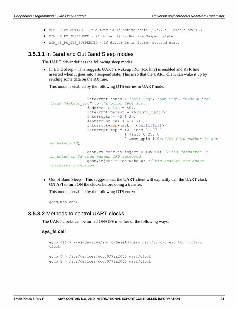
MSM_HS_PM_ACTIVE – if driver is in Active state (i.e., all clocks are ON)
MSM_HS_PM_SUSPENDED – if driver is in Runtime Suspend state
MSM_HS_PM_SYS_SUSPENDED – if driver is in System Suspend state
3.5.3.1 In Band and Out Band Sleep modes
The UART driver defines the following sleep modes:
In Band Sleep – This suggests UART’s wakeup IRQ (RX line) is enabled and RFR line
asserted when it goes into a suspend state. This is so that the UART client can wake it up by
sending some data on the RX line.
This mode is enabled by the following DTS entries in UART node:
Out of Band Sleep – This suggests that the UART client will explicitly call the UART clock
ON API to turn ON the clocks before doing a transfer.
This mode is enabled by the following DTS entry:
qcom,msm-obs;
3.5.3.2 Methods to control UART clocks
The UART clocks can be turned ON/OFF in either of the following ways:
sys_fs call
echo 0|1 > /sys/devices/soc.0/BaseAddress.uart/clock: ex: turn off/on
clock
echo 0 > /sys/devices/soc.0/78af000.uart/clock
echo 1 > /sys/devices/soc.0/78af000.uart/clock
interrupt-names = "core_irq", "bam_irq", "wakeup_irq";
//add "wakeup_irq" to the other IRQs list
#address-cells = <0>;
interrupt-parent = <& blsp1_uart1>; interrupts = <0 1 2>;
#interrupt-cells = <1>;
interrupt-map-mask = <0xffffffff>;
interrupt-map = <0 &intc 0 107 0
1 &intc 0 238 0
2 &msm_gpio 1 0>;//RX GPIO number is set
as Wakeup IRQ
qcom,rx-char-to-inject = <0xFD>; //This character is
injected on TX when wakeup IRQ received
qcom,inject-rx-on-wakeup; //This enables the above
character injection
Peripherals Programming Guide Linux Android Universal Asynchronous Receiver/ Transmitter
LM80-P0436-5 Rev F MAY CONTAIN U.S. AND INTERNATIONAL EXPORT CONTROLLED INFORMATION 32
Kernel API
msm_hs_get_uart_port, msm_hs_request_clock_on|off
Example usage:
IOCTL from the user space
IOCTL cmd
MSM_ENABLE_UART_CLOCK -request clk on
MSM_DISABLE_UART_CLOCK - request clk off
MSM_GET_UART_CLOCK_STATUS - get current status
After turning off the clocks, it is important that no UART functions are called before the clocks
are turned back on, including the UART close function.
3.5.4 Port close
The following call flow shows critical events that occur when the client closes the UART port.
tty_release()-->
uart_close()-->
tty_port_close_start()
<--
msm_hs_stop_rx_locked()
<--
uart_wait_until_sent()-->
msm_hs_tx_empty() returns UART_DM_SR TXEMT
<---
uart_shutdown()-->
uart_update_mctrl()-->
msm_hs_set_mctrl_locked()
<--
uart_port_shutdown()-->
msm_hs_shutdown()
<------
*Can run anytime after msm_hs_stop_rx_locked()
while uart_close()
/* Get the UART Port with port ID */
struct uart_port *port = msm_hs_get_uart_port(0);
/* Request turn off Clocks */
msm_hs_request_clock_off(port);
/* Request turn on clock */
msm_hs_request_clock_on(port);
Peripherals Programming Guide Linux Android Universal Asynchronous Receiver/ Transmitter
LM80-P0436-5 Rev F MAY CONTAIN U.S. AND INTERNATIONAL EXPORT CONTROLLED INFORMATION 33
hsuart_disconnect_rx_endpoint_work()-->
sps_disconnect()--Disconnect/disable BAM connection
and set msm_uport->rx.flush = FLUSH_SHUTDOWN;
<--
The uart_close() function performs the following actions:
Calls tty_port_close_start() to decrement port->counts.
Calls msm_hs_stop_rx_locked():
Clears the RX_BAM_ENABLE bit in UART_DM_DMEN to disable the Rx BAM
interface.
Sets the rx.flush state to FLUSH_STOP.
Schedules the BAM work queue to be disconnected
(hsuart_disconnect_rx_endpoint_work()).
uart_wait_until_sent():
Continuously polls by calling msm_hs_tx_empty() until the UART_DM_SR[TXEMT]
bit is set by the hardware.
Calls uart_shutdown():
Sets the TTY_IO_ERROR bit to tty->flags.
Clears the ASYNCB_INITIALIZED bit to port->flags.
De-asserts RFR, and disables the Auto Ready to Receive bit.
msm_hs_shutdown():
If a Tx is pending (which should not occur), it disables and disconnects by calling
sps_disconnect().
Waits until the hsuart_disconnect_rx_endpoint_work() function runs, and then sets
rx.flush to FLUSH_SHUTDOWN.
Configures the UART hardware:
– UART_DM_CR – Disables the transmitter.
– UART_DM_CR – Disables the receiver.
– UART_DM_IMR – Clears the interrupt mask register.
Turns off the clocks, and sets clk_state to MSM_HS_CLK_PORT_OFF.
Frees IRQ resources.
Releases any GPIO resources.
Frees allocated memory.
Flushes the TTY and LDISC buffers.
LM80-P0436-5 Rev F MAY CONTAIN U.S. AND INTERNATIONAL EXPORT CONTROLLED INFORMATION 34
4 Inter-Integrated Circuit
This chapter describes the Inter-Integrated Circuit (I2C) and explains how to configure it in the
kernel.
4.1 Hardware overview
4.1.1 Qualcomm Universal Serial Engine
The supported mini cores are as follow:
I2C
SPI (see Chapter 5)
I2C core
On the APQ8016E chipset, the Linux I2C driver supports Fast mode plus (up to 1 MHz). The
following key features have been added:
Duty-cycle control
BAM integration
Support for I2C tag version 2
The following features are not supported:
Multi Master mode.
10-bit slave address, and also the 10-bit extend address (for example, 1111 0XX) listed in I2C
specification cannot be used by any slave device.
HS mode(3.4Mhz clock frequency).
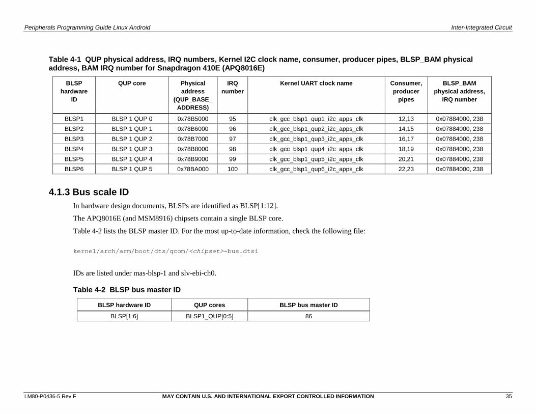
4.1.2 QUP I2C configuration parameters
To match the labeling in the software interface manual, each QUP is identified by a BLSP core
and QUP core (0 to 5). In hardware design documents, BLSPs are identified as BLSP[1:12].
The APQ8016E (and MSM8916) chipsets contain a single BLSP core.
Peripherals Programming Guide Linux Android Inter-Integrated Circuit
LM80-P0436-5 Rev F MAY CONTAIN U.S. AND INTERNATIONAL EXPORT CONTROLLED INFORMATION 35
Table 4-1 QUP physical address, IRQ numbers, Kernel I2C clock name, consumer, producer pipes, BLSP_BAM physical address, BAM IRQ number for Snapdragon 410E (APQ8016E)
BLSP
hardware
ID
QUP core Physical
address
(QUP_BASE_
ADDRESS)
IRQ
number
Kernel UART clock name Consumer,
producer
pipes
BLSP_BAM
physical address,
IRQ number
BLSP1 BLSP 1 QUP 0 0x78B5000 95 clk_gcc_blsp1_qup1_i2c_apps_clk 12,13 0x07884000, 238
BLSP2 BLSP 1 QUP 1 0x78B6000 96 clk_gcc_blsp1_qup2_i2c_apps_clk 14,15 0x07884000, 238
BLSP3 BLSP 1 QUP 2 0x78B7000 97 clk_gcc_blsp1_qup3_i2c_apps_clk 16,17 0x07884000, 238
BLSP4 BLSP 1 QUP 3 0x78B8000 98 clk_gcc_blsp1_qup4_i2c_apps_clk 18,19 0x07884000, 238
BLSP5 BLSP 1 QUP 4 0x78B9000 99 clk_gcc_blsp1_qup5_i2c_apps_clk 20,21 0x07884000, 238
BLSP6 BLSP 1 QUP 5 0x78BA000 100 clk_gcc_blsp1_qup6_i2c_apps_clk 22,23 0x07884000, 238
4.1.3 Bus scale ID
In hardware design documents, BLSPs are identified as BLSP[1:12].
The APQ8016E (and MSM8916) chipsets contain a single BLSP core.
Table 4-2 lists the BLSP master ID. For the most up-to-date information, check the following file:
kernel/arch/arm/boot/dts/qcom/<chipset>-bus.dtsi
IDs are listed under mas-blsp-1 and slv-ebi-ch0.
Table 4-2 BLSP bus master ID
BLSP hardware ID QUP cores BLSP bus master ID
BLSP[1:6] BLSP1_QUP[0:5] 86
Peripherals Programming Guide Linux Android Inter-Integrated Circuit
LM80-P0436-5 Rev F MAY CONTAIN U.S. AND INTERNATIONAL EXPORT CONTROLLED INFORMATION 36
4.2 Configure LK I2C
This section describes how to configure and use any of the available QUP cores in the chipset as
an I2C device.
In the entire LK session, only one QUP core can be used. This means that if BLSP1QUP1 is
already initialized by the LK, BLSP1QUP2 cannot be initialized without a reboot.
The following files are used to configure a QUP core as an I2C in an LK:
/bootable/bootloader/lk/project/<chipset>.mk
/bootable/bootloader/lk/target/<chipset>/init.c
/bootable/bootloader/lk/platform/<chipset>/include/platform/iomap.h
/bootable/bootloader/lk/platform/<chipset>/acpuclock.c
/bootable/bootloader/lk/platform/<chipset>/<chipset>-clock.c
/bootable/bootloader/lk/platform/<chipset>/gpio.c
The following procedure is used for example purposes on an APQ8016E chipset. Similar changes
can be applied to other chipsets.
NOTE: After you try this test, your device will not continue to boot kernel but will be stuck at a fastboot
console accessible via COM port. You will have to boot the device from an SD card by changing
the switch settings to 0100 on DragonBoard 410c and reflash the original binaries to emmc. Then
change the switch back to 0000 to boot from emmc.
1. Enable the console shell to demonstrate I2C.
a. Open the following file:
Project_root/bootable/bootloader/lk/project/<chipset>.mk
b. To demonstrate I2C, create an LK shell program using the serial port.
MODULE +=app/shell
NOTE: This is for testing and demonstration purposes only and is not required for I2C.
c. To test, connect the serial terminal to the device. After compiling is finished, flash the
aboot and reboot the device into fastboot. The following message appears on the
terminal:
console_init: entry
starting app shell
entering main console loop
d. Test the shell by entering help in the terminal program.
Sample output: command list:
help : this list
test : test the command processor
Peripherals Programming Guide Linux Android Inter-Integrated Circuit
LM80-P0436-5 Rev F MAY CONTAIN U.S. AND INTERNATIONAL EXPORT CONTROLLED INFORMATION 37
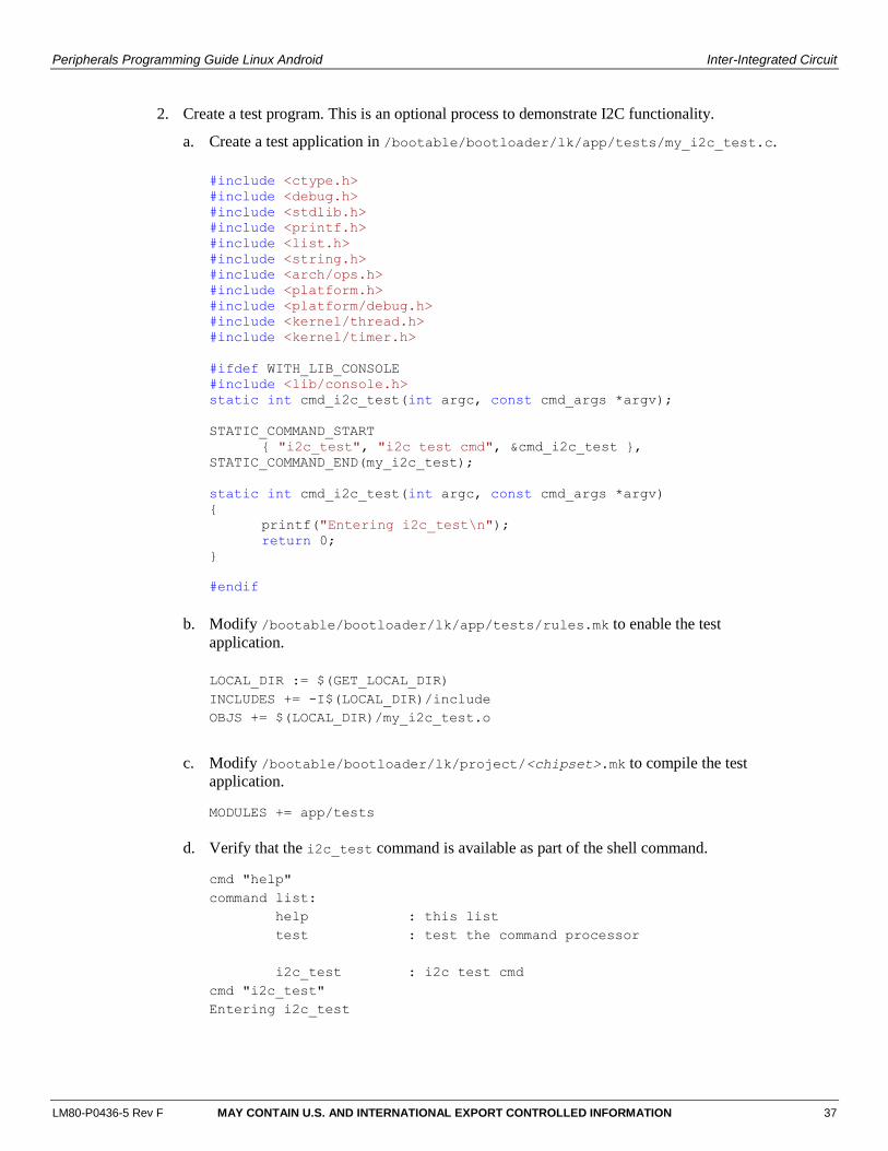
2. Create a test program. This is an optional process to demonstrate I2C functionality.
a. Create a test application in /bootable/bootloader/lk/app/tests/my_i2c_test.c.
b. Modify /bootable/bootloader/lk/app/tests/rules.mk to enable the test
application.
LOCAL_DIR := $(GET_LOCAL_DIR)
INCLUDES += -I$(LOCAL_DIR)/include
OBJS += $(LOCAL_DIR)/my_i2c_test.o
c. Modify /bootable/bootloader/lk/project/<chipset>.mk to compile the test
application.
MODULES += app/tests
d. Verify that the i2c_test command is available as part of the shell command.
cmd "help"
command list:
help : this list
test : test the command processor
i2c_test : i2c test cmd
cmd "i2c_test"
Entering i2c_test
#include <ctype.h>
#include <debug.h>
#include <stdlib.h>
#include <printf.h>
#include <list.h>
#include <string.h>
#include <arch/ops.h>
#include <platform.h>
#include <platform/debug.h>
#include <kernel/thread.h>
#include <kernel/timer.h>
#ifdef WITH_LIB_CONSOLE
#include <lib/console.h>
static int cmd_i2c_test(int argc, const cmd_args *argv);
STATIC_COMMAND_START
{ "i2c_test", "i2c test cmd", &cmd_i2c_test },
STATIC_COMMAND_END(my_i2c_test);
static int cmd_i2c_test(int argc, const cmd_args *argv)
{
printf("Entering i2c_test\n");
return 0;
}
#endif
Peripherals Programming Guide Linux Android Inter-Integrated Circuit
LM80-P0436-5 Rev F MAY CONTAIN U.S. AND INTERNATIONAL EXPORT CONTROLLED INFORMATION 38
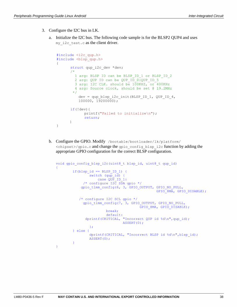
3. Configure the I2C bus in LK.
a. Initialize the I2C bus. The following code sample is for the BLSP2 QUP4 and uses
my_i2c_test.c as the client driver.
b. Configure the GPIO. Modify /bootable/bootloader/lk/platform/
<chipset>/gpio.c and change the gpio_config_blsp_i2c function by adding the
appropriate GPIO configuration for the correct BLSP configuration.
#include <i2c_qup.h>
#include <blsp_qup.h>
{
struct qup_i2c_dev *dev;
/*
1 arg: BLSP ID can be BLSP_ID_1 or BLSP_ID_2
2 arg: QUP ID can be QUP_ID_0:QUP_ID_5
3 arg: I2C CLK. should be 100KHZ, or 400KHz
4 arg: Source clock, should be set @ 19.2MHz
*/
dev = qup_blsp_i2c_init(BLSP_ID_1, QUP_ID_4,
100000, 19200000);
if(!dev){
printf("Failed to initialize\n");
return;
}
}
void gpio_config_blsp_i2c(uint8_t blsp_id, uint8_t qup_id)
{
if(blsp_id == BLSP_ID_1) {
switch (qup_id) {
case QUP_ID_1:
/* configure I2C SDA gpio */
gpio_tlmm_config(6, 3, GPIO_OUTPUT, GPIO_NO_PULL,
GPIO_8MA, GPIO_DISABLE);
/* configure I2C SCL gpio */
gpio_tlmm_config(7, 3, GPIO_OUTPUT, GPIO_NO_PULL,
GPIO_8MA, GPIO_DISABLE);
break;
default:
dprintf(CRITICAL, "Incorrect QUP id %d\n",qup_id);
ASSERT(0);
};
} else {
dprintf(CRITICAL, "Incorrect BLSP id %d\n",blsp_id);
ASSERT(0);
}
}
Peripherals Programming Guide Linux Android Inter-Integrated Circuit
LM80-P0436-5 Rev F MAY CONTAIN U.S. AND INTERNATIONAL EXPORT CONTROLLED INFORMATION 39
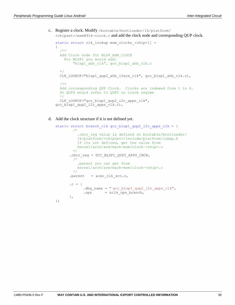
c. Register a clock. Modify /bootable/bootloader/lk/platform/
<chipset>/msm8916-clock.c and add the clock node and corresponding QUP clock.
d. Add the clock structure if it is not defined yet.
static struct clk_lookup msm_clocks_<chip>[] =
{
/**
Add Clock node for BLSP_AHB_CLOCK
For BLSP1 you would add:
"blsp1_ahb_clk", gcc_blsp1_ahb_clk.c
*/
CLK_LOOKUP("blsp1_qup2_ahb_iface_clk", gcc_blsp1_ahb_clk.c),
/**
Add corresponding QUP Clock. Clocks are indexed from 1 to 6.
So QUP4 would refer to QUP5 in clock regime
*/
CLK_LOOKUP("gcc_blsp1_qup2_i2c_apps_clk",
gcc_blsp1_qup2_i2c_apps_clk.c),
static struct branch_clk gcc_blsp1_qup2_i2c_apps_clk = {
/*
.cbcr_reg value is defined on bootable/bootloader/
lk/platform/<chipset>/include/platform/iomap.h
If its not defined, get the value from
kernel/arch/arm/mach-msm/clock-<chip>.c
*/
.cbcr_reg = GCC_BLSP1_QUP2_APPS_CBCR,
/*
.parent you can get from
kernel/arch/arm/mach-msm/clock-<chip>.c
*/
.parent = &cxo_clk_src.c,
.c = {
.dbg_name = " gcc_blsp1_qup2_i2c_apps_clk", .ops = &clk_ops_branch,
},
};
Peripherals Programming Guide Linux Android Inter-Integrated Circuit
LM80-P0436-5 Rev F MAY CONTAIN U.S. AND INTERNATIONAL EXPORT CONTROLLED INFORMATION 40
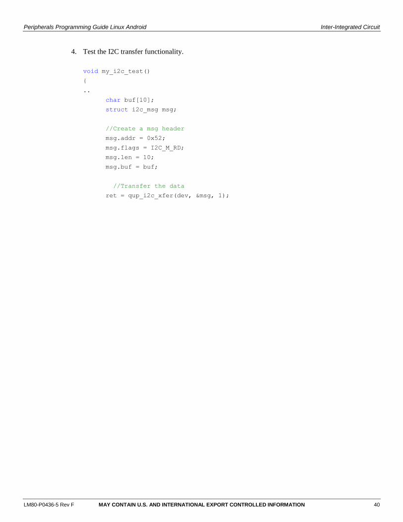
4. Test the I2C transfer functionality.
void my_i2c_test()
{
..
char buf[10];
struct i2c_msg msg;
//Create a msg header
msg.addr = 0x52;
msg.flags = I2C_M_RD;
msg.len = 10;
msg.buf = buf;
//Transfer the data
ret = qup_i2c_xfer(dev, &msg, 1);
Peripherals Programming Guide Linux Android Inter-Integrated Circuit
LM80-P0436-5 Rev F MAY CONTAIN U.S. AND INTERNATIONAL EXPORT CONTROLLED INFORMATION 41
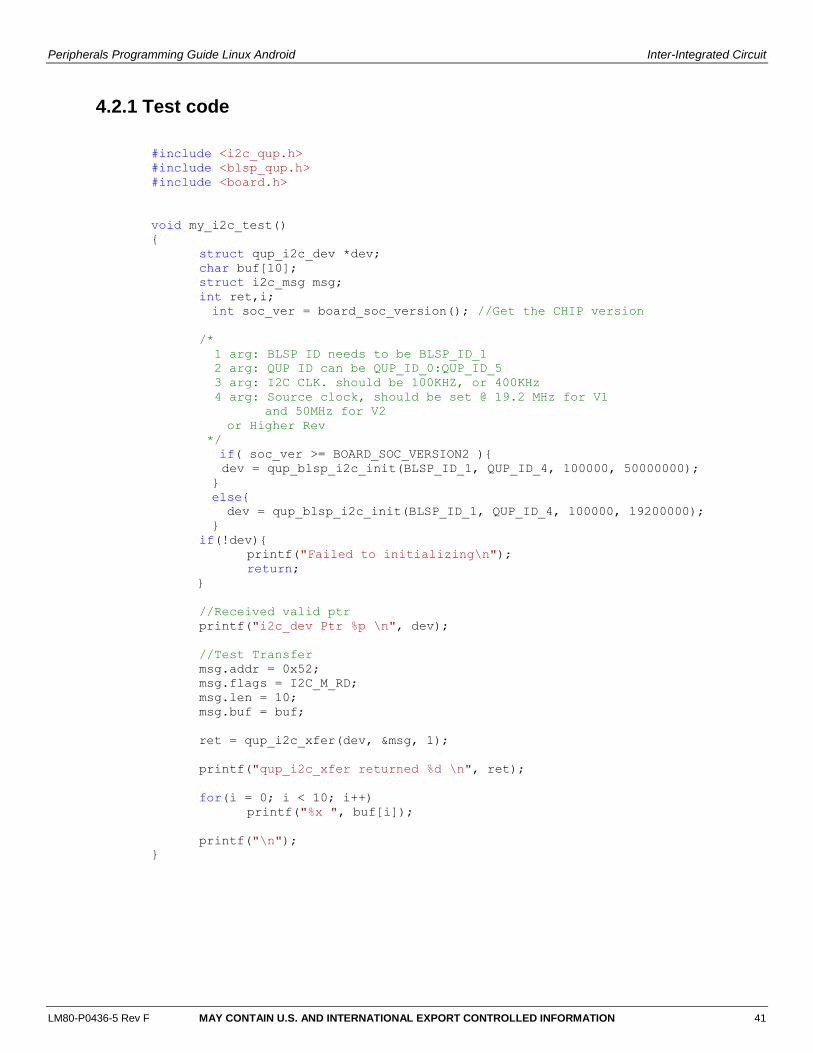
4.2.1 Test code
#include <i2c_qup.h>
#include <blsp_qup.h>
#include <board.h>
void my_i2c_test()
{
struct qup_i2c_dev *dev;
char buf[10];
struct i2c_msg msg;
int ret,i;
int soc_ver = board_soc_version(); //Get the CHIP version
/*
1 arg: BLSP ID needs to be BLSP_ID_1
2 arg: QUP ID can be QUP_ID_0:QUP_ID_5
3 arg: I2C CLK. should be 100KHZ, or 400KHz
4 arg: Source clock, should be set @ 19.2 MHz for V1
and 50MHz for V2
or Higher Rev
*/
if( soc_ver >= BOARD_SOC_VERSION2 ){
dev = qup_blsp_i2c_init(BLSP_ID_1, QUP_ID_4, 100000, 50000000);
}
else{
dev = qup_blsp_i2c_init(BLSP_ID_1, QUP_ID_4, 100000, 19200000);
}
if(!dev){
printf("Failed to initializing\n");
return;
}
//Received valid ptr
printf("i2c_dev Ptr %p \n", dev);
//Test Transfer
msg.addr = 0x52;
msg.flags = I2C_M_RD;
msg.len = 10;
msg.buf = buf;
ret = qup_i2c_xfer(dev, &msg, 1);
printf("qup_i2c_xfer returned %d \n", ret);
for(i = 0; i < 10; i++)
printf("%x ", buf[i]);
printf("\n");
}
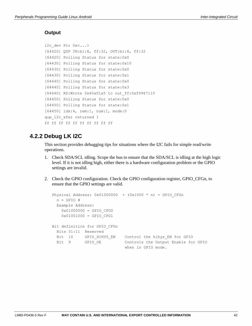
Peripherals Programming Guide Linux Android Inter-Integrated Circuit
LM80-P0436-5 Rev F MAY CONTAIN U.S. AND INTERNATIONAL EXPORT CONTROLLED INFORMATION 42
Output
i2c_dev Ptr 0x<…..>
[64420] QUP IN:bl:8, ff:32, OUT:bl:8, ff:32
[64420] Polling Status for state:0x0
[64430] Polling Status for state:0x10
[64430] Polling Status for state:0x0
[64430] Polling Status for state:0x1
[64440] Polling Status for state:0x0
[64440] Polling Status for state:0x3
[64440] RD:Wrote 0x40a01a5 to out_ff:0xf9967110
[64450] Polling Status for state:0x0
[64450] Polling Status for state:0x1
[64450] idx:4, rem:1, num:1, mode:0
qup_i2c_xfer returned 1
ff ff ff ff ff ff ff ff ff ff
4.2.2 Debug LK I2C
This section provides debugging tips for situations where the I2C fails for simple read/write
operations.
1. Check SDA/SCL idling. Scope the bus to ensure that the SDA/SCL is idling at the high logic
level. If it is not idling high, either there is a hardware configuration problem or the GPIO
settings are invalid.
2. Check the GPIO configuration. Check the GPIO configuration register, GPIO_CFGn, to
ensure that the GPIO settings are valid.
Physical Address: 0x01000000 + (0x1000 * n) = GPIO_CFGn
n = GPIO #
Example Address:
0x01000000 = GPIO_CFG0
0x01001000 = GPIO_CFG1
Bit definition for GPIO_CFGn
Bits 31:11 Reserved
Bit 10 GPIO_HIHYS_EN Control the hihys_EN for GPIO
Bit 9 GPIO_OE Controls the Output Enable for GPIO
when in GPIO mode.
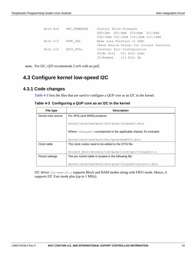
Peripherals Programming Guide Linux Android Inter-Integrated Circuit
LM80-P0436-5 Rev F MAY CONTAIN U.S. AND INTERNATIONAL EXPORT CONTROLLED INFORMATION 43
Bits 8:6 DRV_STRENGTH Control Drive Strength
000:2mA 001:4mA 010:6mA 011:8mA
100:10mA 101:12mA 110:14mA 111:16mA
Bits 5:2 FUNC_SEL Make sure Function is GSBI
Check Device Pinout for Correct Function
Bits 1:0 GPIO_PULL Internal Pull Configuration
00:No Pull 01: Pull Down
10:Keeper 11: Pull Up
NOTE: For I2C, QTI recommends 2 mA with no pull.
4.3 Configure kernel low-speed I2C
4.3.1 Code changes
Table 4-3 lists the files that are used to configure a QUP core as an I2C in the kernel.
Table 4-3 Configuring a QUP core as an I2C in the kernel
File type Description
Device tree source For APQ (and MSM) products:
kernel/arch/arm/boot/dts/qcom/<chipset>.dtsi
Where <chipset> corresponds to the applicable chipset, for example:
kernel/arch/arm/boot/dts/qcom/msm8916.dtsi
Clock table The clock nodes need to be added to the DTSI file.
Project_Root/drivers/clk/qcom/clock-gcc-<chipset>.c
Pinctrl settings The pin control table is located in the following file:
kernel/arch/arm/boot/dts/qcom/<chipset>-pinctrl.dtsi
I2C driver i2c-msm-v2.c supports Block and BAM modes along with FIFO mode. Hence, it
supports I2C Fast mode plus (up to 1 MHz).
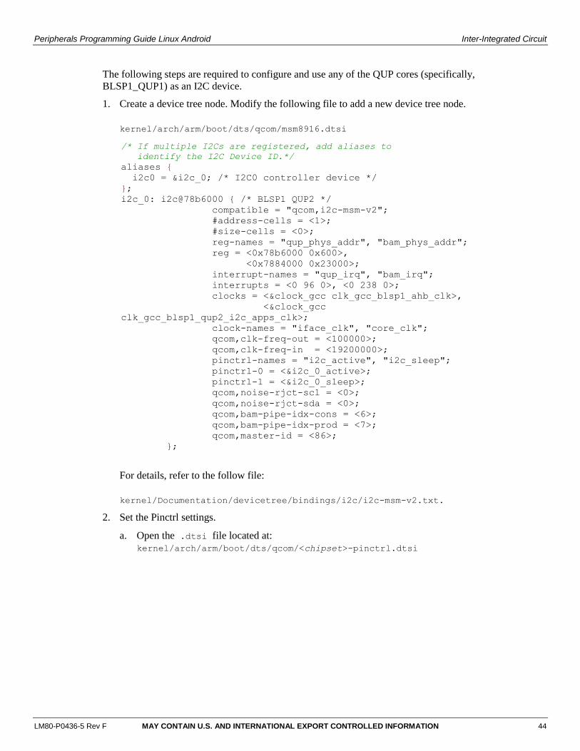
Peripherals Programming Guide Linux Android Inter-Integrated Circuit
LM80-P0436-5 Rev F MAY CONTAIN U.S. AND INTERNATIONAL EXPORT CONTROLLED INFORMATION 44
The following steps are required to configure and use any of the QUP cores (specifically,
BLSP1_QUP1) as an I2C device.
1. Create a device tree node. Modify the following file to add a new device tree node.
kernel/arch/arm/boot/dts/qcom/msm8916.dtsi
For details, refer to the follow file:
kernel/Documentation/devicetree/bindings/i2c/i2c-msm-v2.txt.
2. Set the Pinctrl settings.
a. Open the .dtsi file located at:
kernel/arch/arm/boot/dts/qcom/<chipset>-pinctrl.dtsi
/* If multiple I2Cs are registered, add aliases to
identify the I2C Device ID.*/
aliases {
i2c0 = &i2c_0; /* I2C0 controller device */
};
i2c_0: i2c@78b6000 { /* BLSP1 QUP2 */
compatible = "qcom,i2c-msm-v2";
#address-cells = <1>;
#size-cells = <0>;
reg-names = "qup_phys_addr", "bam_phys_addr";
reg = <0x78b6000 0x600>,
<0x7884000 0x23000>;
interrupt-names = "qup_irq", "bam_irq";
interrupts = <0 96 0>, <0 238 0>;
clocks = <&clock_gcc clk_gcc_blsp1_ahb_clk>,
<&clock_gcc
clk_gcc_blsp1_qup2_i2c_apps_clk>;
clock-names = "iface_clk", "core_clk";
qcom,clk-freq-out = <100000>;
qcom,clk-freq-in = <19200000>;
pinctrl-names = "i2c_active", "i2c_sleep";
pinctrl-0 = <&i2c_0_active>;
pinctrl-1 = <&i2c_0_sleep>;
qcom,noise-rjct-scl = <0>;
qcom,noise-rjct-sda = <0>;
qcom,bam-pipe-idx-cons = <6>;
qcom,bam-pipe-idx-prod = <7>;
qcom,master-id = <86>;
};
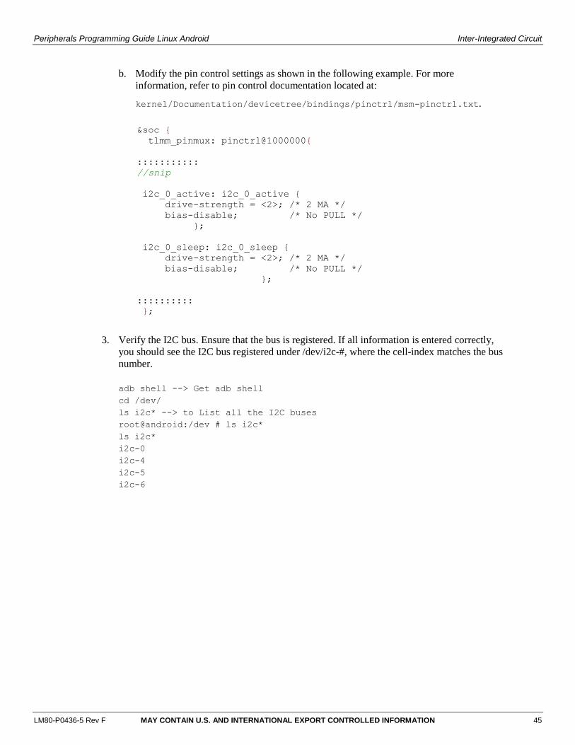
Peripherals Programming Guide Linux Android Inter-Integrated Circuit
LM80-P0436-5 Rev F MAY CONTAIN U.S. AND INTERNATIONAL EXPORT CONTROLLED INFORMATION 45
b. Modify the pin control settings as shown in the following example. For more
information, refer to pin control documentation located at:
kernel/Documentation/devicetree/bindings/pinctrl/msm-pinctrl.txt.
3. Verify the I2C bus. Ensure that the bus is registered. If all information is entered correctly,
you should see the I2C bus registered under /dev/i2c-#, where the cell-index matches the bus
number.
adb shell --> Get adb shell
cd /dev/
ls i2c* --> to List all the I2C buses
root@android:/dev # ls i2c*
ls i2c*
i2c-0
i2c-4
i2c-5
i2c-6
&soc {
tlmm_pinmux: pinctrl@1000000{
:::::::::::
//snip
i2c_0_active: i2c_0_active {
drive-strength = <2>; /* 2 MA */
bias-disable; /* No PULL */
};
i2c_0_sleep: i2c_0_sleep {
drive-strength = <2>; /* 2 MA */
bias-disable; /* No PULL */
};
::::::::::
};
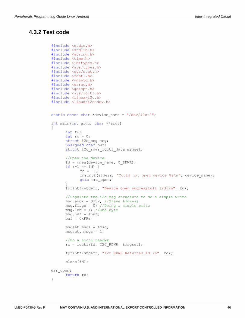
Peripherals Programming Guide Linux Android Inter-Integrated Circuit
LM80-P0436-5 Rev F MAY CONTAIN U.S. AND INTERNATIONAL EXPORT CONTROLLED INFORMATION 46
4.3.2 Test code
#include <stdio.h>
#include <stdlib.h>
#include <string.h>
#include <time.h>
#include <inttypes.h>
#include <sys/types.h>
#include <sys/stat.h>
#include <fcntl.h>
#include <unistd.h>
#include <errno.h>
#include <getopt.h>
#include <sys/ioctl.h>
#include <linux/i2c.h>
#include <linux/i2c-dev.h>
static const char *device_name = "/dev/i2c-2";
int main(int argc, char **argv)
{
int fd;
int rc = 0;
struct i2c_msg msg;
unsigned char buf;
struct i2c_rdwr_ioctl_data msgset;
//Open the device
fd = open(device_name, O_RDWR);
if (-1 == fd) {
rc = -1;
fprintf(stderr, "Could not open device %s\n", device_name);
goto err_open;
}
fprintf(stderr, "Device Open successfull [%d]\n", fd);
//Populate the i2c msg structure to do a simple write
msg.addr = 0x52; //Slave Address
msg.flags = 0; //Doing a simple write
msg.len = 1; //One byte
msg.buf = &buf;
buf = 0xFF;
msgset.msgs = &msg;
msgset.nmsgs = 1;
//Do a ioctl readwr
rc = ioctl(fd, I2C_RDWR, &msgset);
fprintf(stderr, "I2C RDWR Returned %d \n", rc);
close(fd);
err_open:
return rc;
}
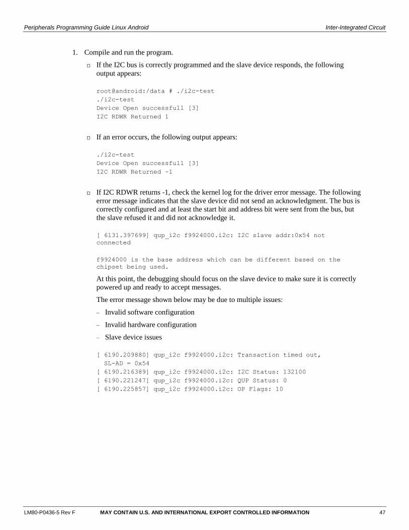
Peripherals Programming Guide Linux Android Inter-Integrated Circuit
LM80-P0436-5 Rev F MAY CONTAIN U.S. AND INTERNATIONAL EXPORT CONTROLLED INFORMATION 47
1. Compile and run the program.
If the I2C bus is correctly programmed and the slave device responds, the following
output appears:
root@android:/data # ./i2c-test
./i2c-test
Device Open successfull [3]
I2C RDWR Returned 1
If an error occurs, the following output appears:
./i2c-test
Device Open successfull [3]
I2C RDWR Returned -1
If I2C RDWR returns -1, check the kernel log for the driver error message. The following
error message indicates that the slave device did not send an acknowledgment. The bus is
correctly configured and at least the start bit and address bit were sent from the bus, but
the slave refused it and did not acknowledge it.
[ 6131.397699] qup_i2c f9924000.i2c: I2C slave addr:0x54 not
connected
f9924000 is the base address which can be different based on the
chipset being used.
At this point, the debugging should focus on the slave device to make sure it is correctly
powered up and ready to accept messages.
The error message shown below may be due to multiple issues:
– Invalid software configuration
– Invalid hardware configuration
– Slave device issues
[ 6190.209880] qup_i2c f9924000.i2c: Transaction timed out,
SL-AD = 0x54
[ 6190.216389] qup_i2c f9924000.i2c: I2C Status: 132100
[ 6190.221247] qup_i2c f9924000.i2c: QUP Status: 0
[ 6190.225857] qup_i2c f9924000.i2c: OP Flags: 10
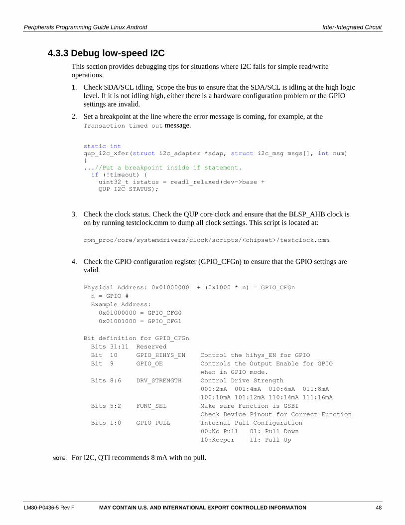
Peripherals Programming Guide Linux Android Inter-Integrated Circuit
LM80-P0436-5 Rev F MAY CONTAIN U.S. AND INTERNATIONAL EXPORT CONTROLLED INFORMATION 48
4.3.3 Debug low-speed I2C
This section provides debugging tips for situations where I2C fails for simple read/write
operations.
1. Check SDA/SCL idling. Scope the bus to ensure that the SDA/SCL is idling at the high logic
level. If it is not idling high, either there is a hardware configuration problem or the GPIO
settings are invalid.
2. Set a breakpoint at the line where the error message is coming, for example, at the
Transaction timed out message.
3. Check the clock status. Check the QUP core clock and ensure that the BLSP_AHB clock is
on by running testclock.cmm to dump all clock settings. This script is located at:
rpm_proc/core/systemdrivers/clock/scripts/<chipset>/testclock.cmm
4. Check the GPIO configuration register (GPIO_CFGn) to ensure that the GPIO settings are
valid.
Physical Address: 0x01000000 + (0x1000 * n) = GPIO_CFGn
n = GPIO #
Example Address:
0x01000000 = GPIO_CFG0
0x01001000 = GPIO_CFG1
Bit definition for GPIO_CFGn
Bits 31:11 Reserved
Bit 10 GPIO_HIHYS_EN Control the hihys_EN for GPIO
Bit 9 GPIO_OE Controls the Output Enable for GPIO
when in GPIO mode.
Bits 8:6 DRV_STRENGTH Control Drive Strength
000:2mA 001:4mA 010:6mA 011:8mA
100:10mA 101:12mA 110:14mA 111:16mA
Bits 5:2 FUNC_SEL Make sure Function is GSBI
Check Device Pinout for Correct Function
Bits 1:0 GPIO_PULL Internal Pull Configuration
00:No Pull 01: Pull Down
10:Keeper 11: Pull Up
NOTE: For I2C, QTI recommends 8 mA with no pull.
static int
qup_i2c_xfer(struct i2c_adapter *adap, struct i2c_msg msgs[], int num)
{
...//Put a breakpoint inside if statement.
if (!timeout) {
uint32_t istatus = readl_relaxed(dev->base +
QUP_I2C_STATUS);
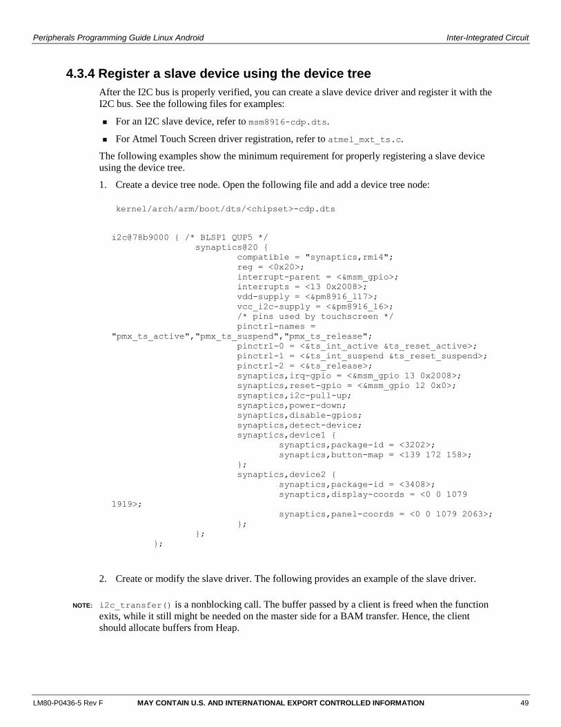
Peripherals Programming Guide Linux Android Inter-Integrated Circuit
LM80-P0436-5 Rev F MAY CONTAIN U.S. AND INTERNATIONAL EXPORT CONTROLLED INFORMATION 49
4.3.4 Register a slave device using the device tree
After the I2C bus is properly verified, you can create a slave device driver and register it with the
I2C bus. See the following files for examples:
For an I2C slave device, refer to msm8916-cdp.dts.
For Atmel Touch Screen driver registration, refer to atmel_mxt_ts.c.
The following examples show the minimum requirement for properly registering a slave device
using the device tree.
1. Create a device tree node. Open the following file and add a device tree node:
kernel/arch/arm/boot/dts/<chipset>-cdp.dts
2. Create or modify the slave driver. The following provides an example of the slave driver.
NOTE: i2c_transfer() is a nonblocking call. The buffer passed by a client is freed when the function
exits, while it still might be needed on the master side for a BAM transfer. Hence, the client
should allocate buffers from Heap.
i2c@78b9000 { /* BLSP1 QUP5 */
synaptics@20 {
compatible = "synaptics,rmi4";
reg = <0x20>;
interrupt-parent = <&msm_gpio>;
interrupts = <13 0x2008>;
vdd-supply = <&pm8916_l17>;
vcc_i2c-supply = <&pm8916_l6>;
/* pins used by touchscreen */
pinctrl-names =
"pmx_ts_active","pmx_ts_suspend","pmx_ts_release";
pinctrl-0 = <&ts_int_active &ts_reset_active>;
pinctrl-1 = <&ts_int_suspend &ts_reset_suspend>;
pinctrl-2 = <&ts_release>;
synaptics,irq-gpio = <&msm_gpio 13 0x2008>;
synaptics,reset-gpio = <&msm_gpio 12 0x0>;
synaptics,i2c-pull-up;
synaptics,power-down;
synaptics,disable-gpios;
synaptics,detect-device;
synaptics,device1 {
synaptics,package-id = <3202>;
synaptics,button-map = <139 172 158>;
};
synaptics,device2 {
synaptics,package-id = <3408>;
synaptics,display-coords = <0 0 1079
1919>;
synaptics,panel-coords = <0 0 1079 2063>;
};
};
};
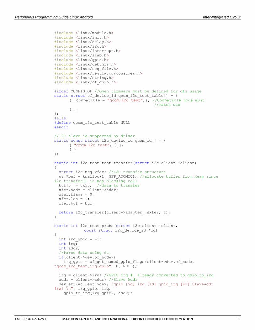
Peripherals Programming Guide Linux Android Inter-Integrated Circuit
LM80-P0436-5 Rev F MAY CONTAIN U.S. AND INTERNATIONAL EXPORT CONTROLLED INFORMATION 50
#include <linux/module.h>
#include <linux/init.h>
#include <linux/delay.h>
#include <linux/i2c.h>
#include <linux/interrupt.h>
#include <linux/slab.h>
#include <linux/gpio.h>
#include <linux/debugfs.h>
#include <linux/seq_file.h>
#include <linux/regulator/consumer.h>
#include <linux/string.h>
#include <linux/of_gpio.h>
#ifdef CONFIG_OF //Open firmware must be defined for dts usage
static struct of_device_id qcom_i2c_test_table[] = {
{ .compatible = "qcom,i2c-test",}, //Compatible node must
//match dts
{ },
};
#else
#define qcom_i2c_test_table NULL
#endif
//I2C slave id supported by driver
static const struct i2c_device_id qcom_id[] = {
{ "qcom_i2c_test", 0 },
{ }
};
static int i2c_test_test_transfer(struct i2c_client *client)
{
struct i2c_msg xfer; //I2C transfer structure
u8 *buf = kmalloc(1, GFP_ATOMIC); //allocate buffer from Heap since
i2c_transfer() is non-blocking call
buf[0] = 0x55; //data to transfer
xfer.addr = client->addr;
xfer.flags = 0;
xfer.len = 1;
xfer.buf = buf;
return i2c_transfer(client->adapter, &xfer, 1);
}
static int i2c_test_probe(struct i2c_client *client,
const struct i2c_device_id *id)
{
int irq_gpio = -1;
int irq;
int addr;
//Parse data using dt.
if(client->dev.of_node){
irq_gpio = of_get_named_gpio_flags(client->dev.of_node,
"qcom_i2c_test,irq-gpio", 0, NULL);
}
irq = client->irq; //GPIO irq #. already converted to gpio_to_irq
addr = client->addr; //Slave Addr
dev_err(&client->dev, "gpio [%d] irq [%d] gpio_irq [%d] Slaveaddr
[%x] \n", irq_gpio, irq,
gpio_to_irq(irq_gpio), addr);
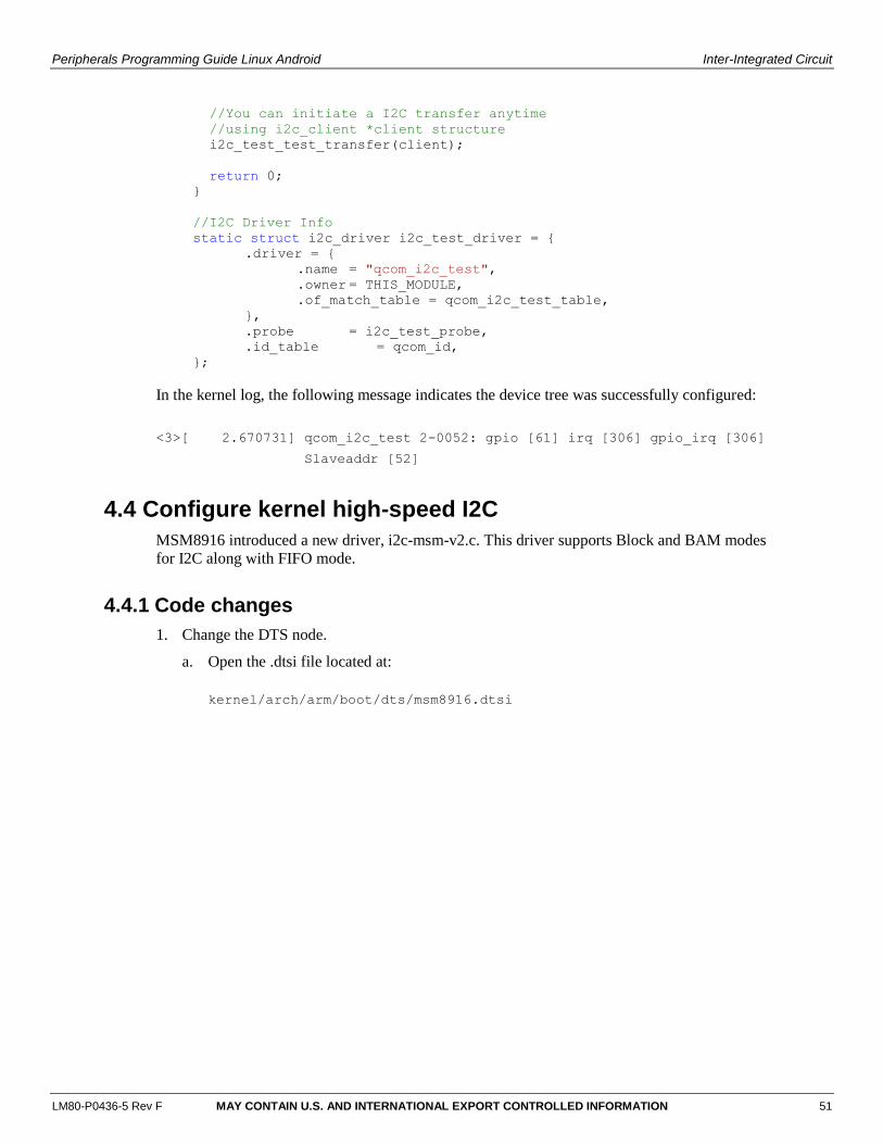
Peripherals Programming Guide Linux Android Inter-Integrated Circuit
LM80-P0436-5 Rev F MAY CONTAIN U.S. AND INTERNATIONAL EXPORT CONTROLLED INFORMATION 51
In the kernel log, the following message indicates the device tree was successfully configured:
<3>[ 2.670731] qcom_i2c_test 2-0052: gpio [61] irq [306] gpio_irq [306]
Slaveaddr [52]
4.4 Configure kernel high-speed I2C
MSM8916 introduced a new driver, i2c-msm-v2.c. This driver supports Block and BAM modes
for I2C along with FIFO mode.
4.4.1 Code changes
1. Change the DTS node.
a. Open the .dtsi file located at:
kernel/arch/arm/boot/dts/msm8916.dtsi
//You can initiate a I2C transfer anytime
//using i2c_client *client structure
i2c_test_test_transfer(client);
return 0;
}
//I2C Driver Info
static struct i2c_driver i2c_test_driver = {
.driver = {
.name = "qcom_i2c_test",
.owner = THIS_MODULE,
.of_match_table = qcom_i2c_test_table,
},
.probe = i2c_test_probe,
.id_table = qcom_id,
};
//Easy wrapper to do driver init
module_i2c_driver(i2c_test_driver);
MODULE_DESCRIPTION("I2C TEST");
MODULE_LICENSE("GPL v2");
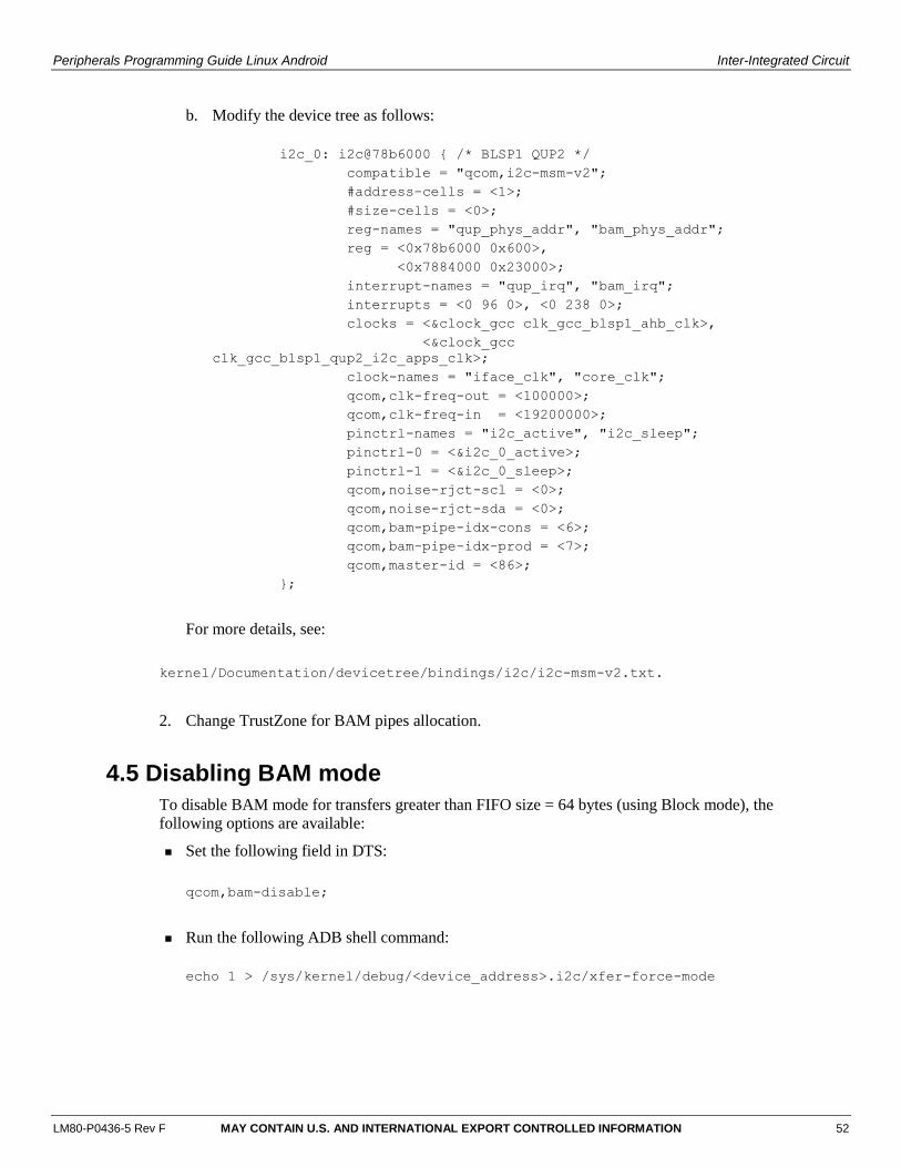
Peripherals Programming Guide Linux Android Inter-Integrated Circuit
LM80-P0436-5 Rev F MAY CONTAIN U.S. AND INTERNATIONAL EXPORT CONTROLLED INFORMATION 52
b. Modify the device tree as follows:
i2c_0: i2c@78b6000 { /* BLSP1 QUP2 */
compatible = "qcom,i2c-msm-v2";
#address-cells = <1>;
#size-cells = <0>;
reg-names = "qup_phys_addr", "bam_phys_addr";
reg = <0x78b6000 0x600>,
<0x7884000 0x23000>;
interrupt-names = "qup_irq", "bam_irq";
interrupts = <0 96 0>, <0 238 0>;
clocks = <&clock_gcc clk_gcc_blsp1_ahb_clk>,
<&clock_gcc
clk_gcc_blsp1_qup2_i2c_apps_clk>;
clock-names = "iface_clk", "core_clk";
qcom,clk-freq-out = <100000>;
qcom,clk-freq-in = <19200000>;
pinctrl-names = "i2c_active", "i2c_sleep";
pinctrl-0 = <&i2c_0_active>;
pinctrl-1 = <&i2c_0_sleep>;
qcom,noise-rjct-scl = <0>;
qcom,noise-rjct-sda = <0>;
qcom,bam-pipe-idx-cons = <6>;
qcom,bam-pipe-idx-prod = <7>;
qcom,master-id = <86>;
};
For more details, see:
kernel/Documentation/devicetree/bindings/i2c/i2c-msm-v2.txt.
2. Change TrustZone for BAM pipes allocation.
4.5 Disabling BAM mode
To disable BAM mode for transfers greater than FIFO size = 64 bytes (using Block mode), the
following options are available:
Set the following field in DTS:
qcom,bam-disable;
Run the following ADB shell command:
echo 1 > /sys/kernel/debug/<device_address>.i2c/xfer-force-mode
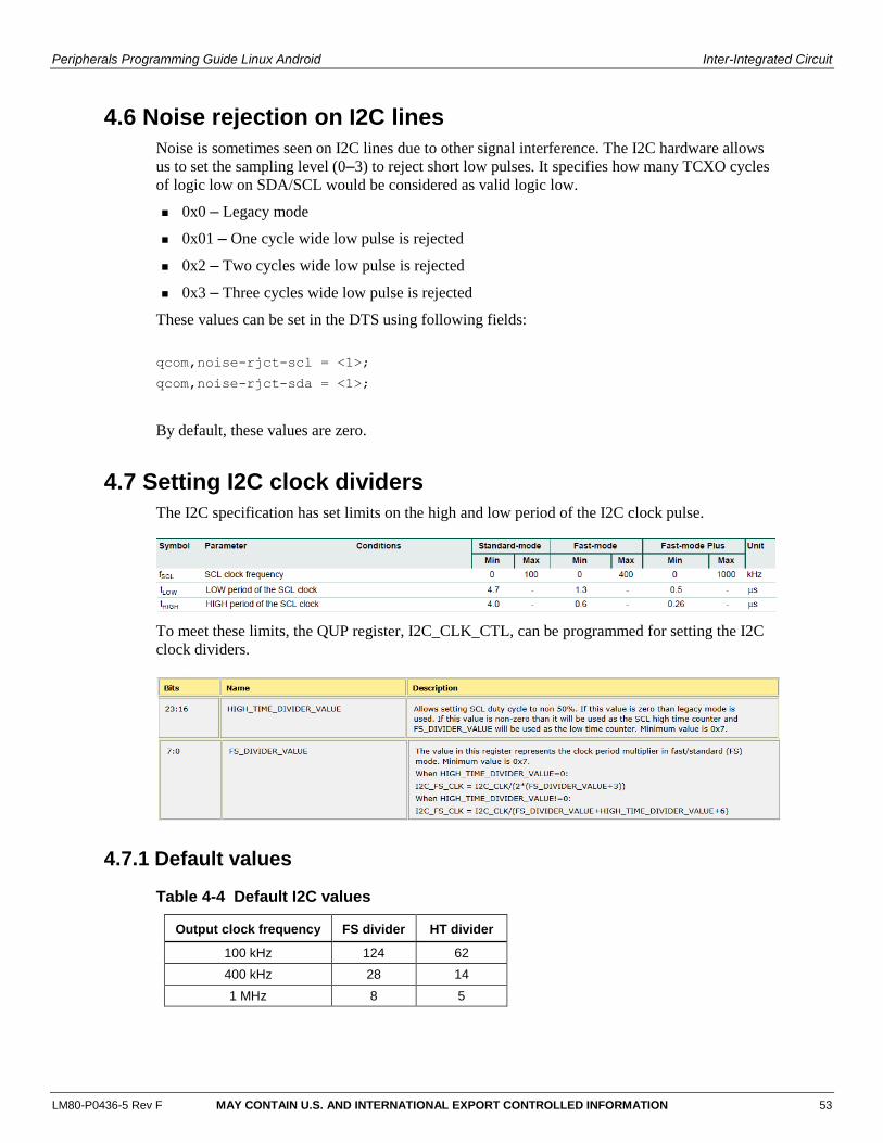
Peripherals Programming Guide Linux Android Inter-Integrated Circuit
LM80-P0436-5 Rev F MAY CONTAIN U.S. AND INTERNATIONAL EXPORT CONTROLLED INFORMATION 53
4.6 Noise rejection on I2C lines
Noise is sometimes seen on I2C lines due to other signal interference. The I2C hardware allows
us to set the sampling level (0–3) to reject short low pulses. It specifies how many TCXO cycles
of logic low on SDA/SCL would be considered as valid logic low.
0x0 – Legacy mode
0x01 – One cycle wide low pulse is rejected
0x2 – Two cycles wide low pulse is rejected
0x3 – Three cycles wide low pulse is rejected
These values can be set in the DTS using following fields:
qcom,noise-rjct-scl = <1>;
qcom,noise-rjct-sda = <1>;
By default, these values are zero.
4.7 Setting I2C clock dividers
The I2C specification has set limits on the high and low period of the I2C clock pulse.
To meet these limits, the QUP register, I2C_CLK_CTL, can be programmed for setting the I2C
clock dividers.
4.7.1 Default values
Table 4-4 Default I2C values
Output clock frequency FS divider HT divider
100 kHz 124 62
400 kHz 28 14
1 MHz 8 5
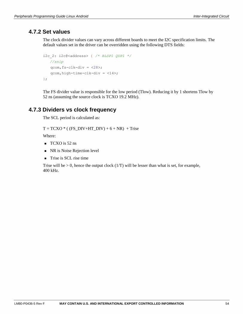
Peripherals Programming Guide Linux Android Inter-Integrated Circuit
LM80-P0436-5 Rev F MAY CONTAIN U.S. AND INTERNATIONAL EXPORT CONTROLLED INFORMATION 54
4.7.2 Set values
The clock divider values can vary across different boards to meet the I2C specification limits. The
default values set in the driver can be overridden using the following DTS fields:
i2c_2: i2c@<address> { /* BLSP1 QUP1 */
//snip
qcom,fs-clk-div = <28>;
qcom,high-time-clk-div = <14>;
};
The FS divider value is responsible for the low period (Tlow). Reducing it by 1 shortens Tlow by
52 ns (assuming the source clock is TCXO 19.2 MHz).
4.7.3 Dividers vs clock frequency
The SCL period is calculated as:
T = TCXO * ( (FS_DIV+HT_DIV) + 6 + NR) + Trise
Where:
TCXO is 52 ns
NR is Noise Rejection level
Trise is SCL rise time
Trise will be > 0, hence the output clock (1/T) will be lesser than what is set, for example,
400 kHz.
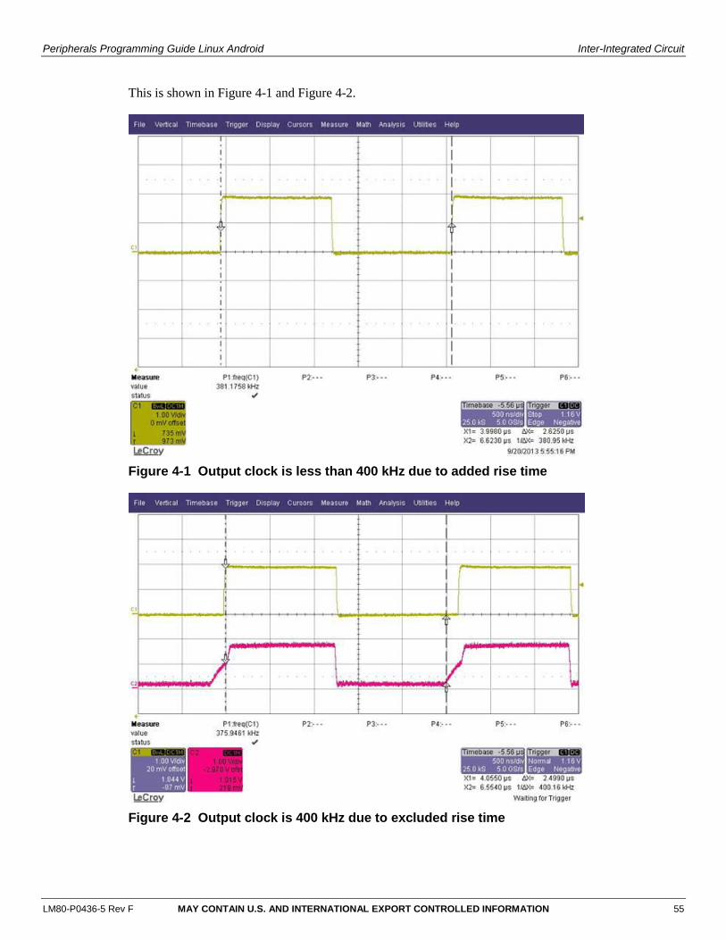
Peripherals Programming Guide Linux Android Inter-Integrated Circuit
LM80-P0436-5 Rev F MAY CONTAIN U.S. AND INTERNATIONAL EXPORT CONTROLLED INFORMATION 55
This is shown in Figure 4-1 and Figure 4-2.
Figure 4-1 Output clock is less than 400 kHz due to added rise time
Figure 4-2 Output clock is 400 kHz due to excluded rise time
Peripherals Programming Guide Linux Android Inter-Integrated Circuit
LM80-P0436-5 Rev F MAY CONTAIN U.S. AND INTERNATIONAL EXPORT CONTROLLED INFORMATION 56
The divider ratio, FS_DIV/HTD, should be 2:1. Adjust the divider values to maintain this ratio
and get a lesser sum so that a higher output clock can be generated.
4.8 I2C power management
I2C slave devices must register system suspend/resume (SYSTEM_PM_OPS) handlers with the
power management framework to ensure that no I2C transactions are initiated after the I2C
master is suspended.
Example
/* Register PM Hooks */
static const struct dev_pm_ops i2c_test_pm_ops = {
SET_SYSTEM_SLEEP_PM_OPS(
i2c_test_suspend, //Get call when suspend is happening
i2c_test_resume //Get call when resume is happening
)
};
//I2C Driver Info
static struct i2c_driver i2c_test_driver = {
.driver = {
.pm = &i2c_test_pm_ops,
},
.probe = i2c_test_probe,
.id_table = qcom_id,
};
/* System Going to Suspend*/
static int i2c_test_suspend(struct device *device)
{
/*
* Properly set slave device to suspend (I2C transactions are OK)
* Set a suspend flag
* No more I2C transaction should occur until i2c_test_resume is called
*/
return 0;
}
static int i2c_test_resume(struct device *device)
{
/*
* Remove slave device from suspend (I2C transactions are OK)
* Clear suspend flag
*/
return 0;
}
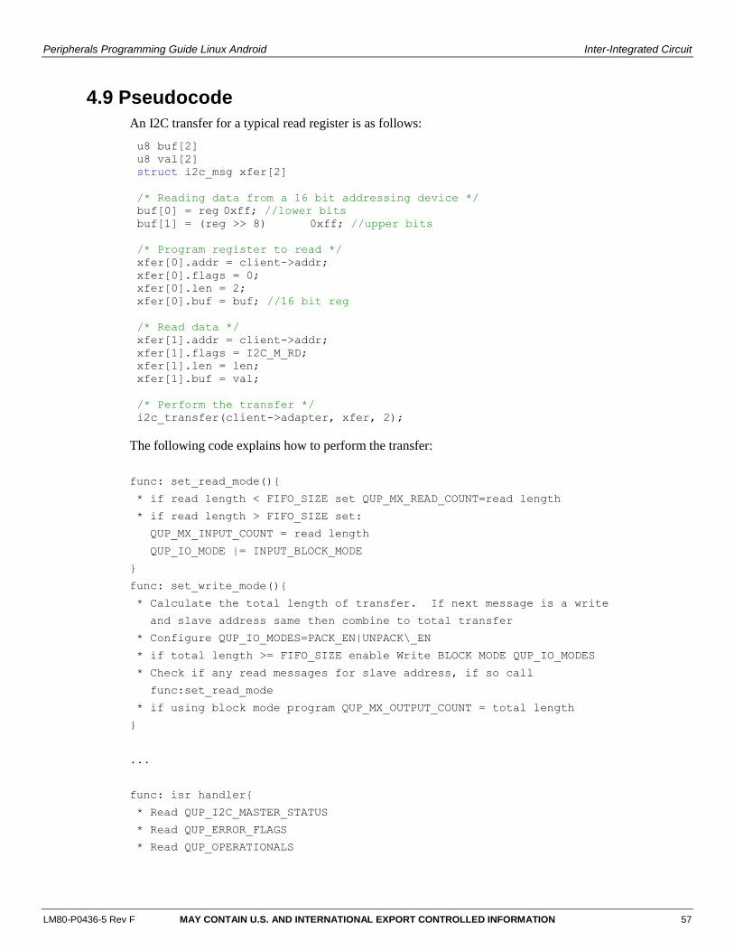
Peripherals Programming Guide Linux Android Inter-Integrated Circuit
LM80-P0436-5 Rev F MAY CONTAIN U.S. AND INTERNATIONAL EXPORT CONTROLLED INFORMATION 57
4.9 Pseudocode
An I2C transfer for a typical read register is as follows:
The following code explains how to perform the transfer:
func: set_read_mode(){
* if read length < FIFO_SIZE set QUP_MX_READ_COUNT=read length
* if read length > FIFO_SIZE set:
QUP_MX_INPUT_COUNT = read length
QUP_IO_MODE |= INPUT_BLOCK_MODE
}
func: set_write_mode(){
* Calculate the total length of transfer. If next message is a write
and slave address same then combine to total transfer
* Configure QUP_IO_MODES=PACK_EN|UNPACK\_EN
* if total length >= FIFO_SIZE enable Write BLOCK MODE QUP_IO_MODES
* Check if any read messages for slave address, if so call
func:set_read_mode
* if using block mode program QUP_MX_OUTPUT_COUNT = total length
}
...
func: isr handler{
* Read QUP_I2C_MASTER_STATUS
* Read QUP_ERROR_FLAGS
* Read QUP_OPERATIONALS
u8 buf[2]
u8 val[2]
struct i2c_msg xfer[2]
/* Reading data from a 16 bit addressing device */
buf[0] = reg 0xff; //lower bits
buf[1] = (reg >> 8) 0xff; //upper bits
/* Program register to read */
xfer[0].addr = client->addr;
xfer[0].flags = 0;
xfer[0].len = 2;
xfer[0].buf = buf; //16 bit reg
/* Read data */
xfer[1].addr = client->addr;
xfer[1].flags = I2C_M_RD;
xfer[1].len = len;
xfer[1].buf = val;
/* Perform the transfer */
i2c_transfer(client->adapter, xfer, 2);
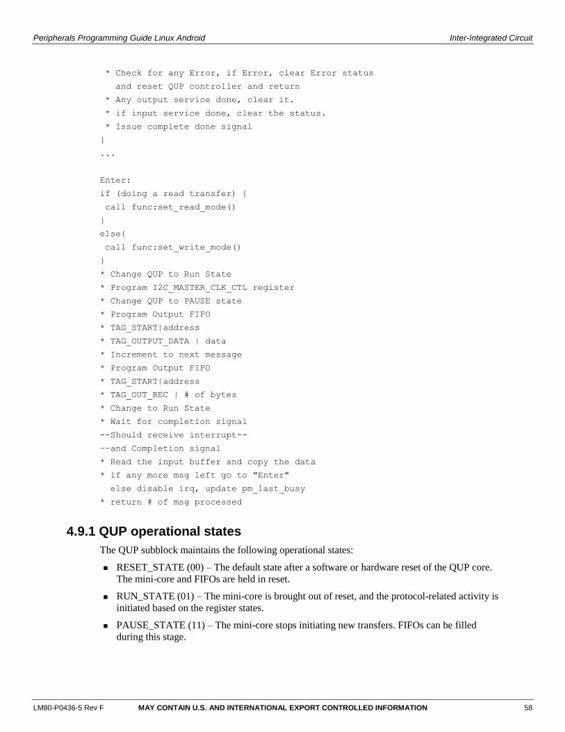
Peripherals Programming Guide Linux Android Inter-Integrated Circuit
LM80-P0436-5 Rev F MAY CONTAIN U.S. AND INTERNATIONAL EXPORT CONTROLLED INFORMATION 58
* Check for any Error, if Error, clear Error status
and reset QUP controller and return
* Any output service done, clear it.
* if input service done, clear the status.
* Issue complete done signal
}
...
Enter:
if (doing a read transfer) {
call func:set_read_mode()
}
else{
call func:set_write_mode()
}
* Change QUP to Run State
* Program I2C_MASTER_CLK_CTL register
* Change QUP to PAUSE state
* Program Output FIFO
* TAG_START|address
* TAG_OUTPUT_DATA | data
* Increment to next message
* Program Output FIFO
* TAG_START|address
* TAG_OUT_REC | # of bytes
* Change to Run State
* Wait for completion signal
--Should receive interrupt--
--and Completion signal
* Read the input buffer and copy the data
* if any more msg left go to "Enter"
else disable irq, update pm_last_busy
* return # of msg processed
4.9.1 QUP operational states
The QUP subblock maintains the following operational states:
RESET_STATE (00) – The default state after a software or hardware reset of the QUP core.
The mini-core and FIFOs are held in reset.
RUN_STATE (01) – The mini-core is brought out of reset, and the protocol-related activity is
initiated based on the register states.
PAUSE_STATE (11) – The mini-core stops initiating new transfers. FIFOs can be filled
during this stage.
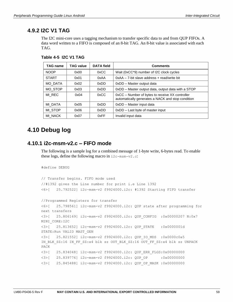
Peripherals Programming Guide Linux Android Inter-Integrated Circuit
LM80-P0436-5 Rev F MAY CONTAIN U.S. AND INTERNATIONAL EXPORT CONTROLLED INFORMATION 59
4.9.2 I2C V1 TAG
The I2C mini-core uses a tagging mechanism to transfer specific data to and from QUP FIFOs. A
data word written to a FIFO is composed of an 8-bit TAG. An 8-bit value is associated with each
TAG.
Table 4-5 I2C V1 TAG
TAG name TAG value DATA field Comments
NOOP 0x00 0xCC Wait (0xCC*9) number of I2C clock cycles
START 0x01 0xAA 0xAA – 7-bit slave address + read/write bit
MO_DATA 0x02 0xDD 0xDD – Master output data
MO_STOP 0x03 0xDD 0xDD – Master output data, output data with a STOP
MI_REC 0x04 0xCC 0xCC – Number of bytes to receive XX controller automatically generates a NACK and stop condition
MI_DATA 0x05 0xDD 0xDD – Master input data
MI_STOP 0x06 0xDD 0xDD – Last byte of master input
MI_NACK 0x07 0xFF Invalid input data
4.10 Debug log
4.10.1 i2c-msm-v2.c – FIFO mode
The following is a sample log for a combined message of 1-byte write, 6-bytes read. To enable
these logs, define the following macro in i2c-msm-v2.c:
#define DEBUG
// Transfer begins. FIFO mode used
//#1392 gives the Line number for print i.e Line 1392
<6>[ 25.792522] i2c-msm-v2 f9924000.i2c: #1392 Starting FIFO transfer
//Programmed Registers for transfer
<6>[ 25.798561] i2c-msm-v2 f9924000.i2c: QUP state after programming for
next transfers
<3>[ 25.806169] i2c-msm-v2 f9924000.i2c: QUP_CONFIG :0x00000207 N:0x7
MINI_CORE:I2C
<3>[ 25.813652] i2c-msm-v2 f9924000.i2c: QUP_STATE :0x0000001d
STATE:Run VALID MAST_GEN
<3>[ 25.821552] i2c-msm-v2 f9924000.i2c: QUP_IO_MDS :0x0000c0a5
IN_BLK_SZ:16 IN_FF_SZ:x4 blk sz OUT_BLK_SZ:16 OUT_FF_SZ:x4 blk sz UNPACK
PACK
<3>[ 25.834048] i2c-msm-v2 f9924000.i2c: QUP_ERR_FLGS:0x00000000
<3>[ 25.839776] i2c-msm-v2 f9924000.i2c: QUP_OP :0x00000000
<3>[ 25.845488] i2c-msm-v2 f9924000.i2c: QUP_OP_MASK :0x00000000
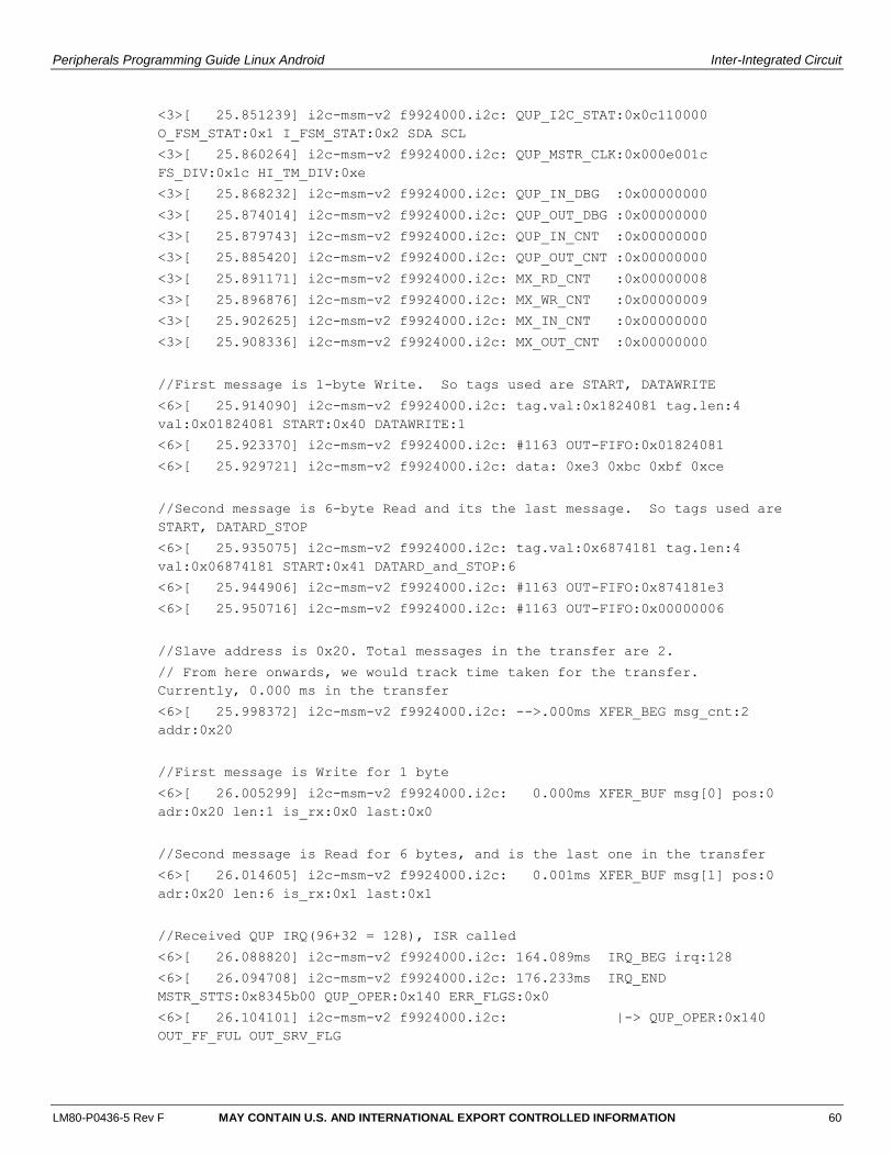
Peripherals Programming Guide Linux Android Inter-Integrated Circuit
LM80-P0436-5 Rev F MAY CONTAIN U.S. AND INTERNATIONAL EXPORT CONTROLLED INFORMATION 60
<3>[ 25.851239] i2c-msm-v2 f9924000.i2c: QUP_I2C_STAT:0x0c110000
O_FSM_STAT:0x1 I_FSM_STAT:0x2 SDA SCL
<3>[ 25.860264] i2c-msm-v2 f9924000.i2c: QUP_MSTR_CLK:0x000e001c
FS_DIV:0x1c HI_TM_DIV:0xe
<3>[ 25.868232] i2c-msm-v2 f9924000.i2c: QUP_IN_DBG :0x00000000
<3>[ 25.874014] i2c-msm-v2 f9924000.i2c: QUP_OUT_DBG :0x00000000
<3>[ 25.879743] i2c-msm-v2 f9924000.i2c: QUP_IN_CNT :0x00000000
<3>[ 25.885420] i2c-msm-v2 f9924000.i2c: QUP_OUT_CNT :0x00000000
<3>[ 25.891171] i2c-msm-v2 f9924000.i2c: MX_RD_CNT :0x00000008
<3>[ 25.896876] i2c-msm-v2 f9924000.i2c: MX_WR_CNT :0x00000009
<3>[ 25.902625] i2c-msm-v2 f9924000.i2c: MX_IN_CNT :0x00000000
<3>[ 25.908336] i2c-msm-v2 f9924000.i2c: MX_OUT_CNT :0x00000000
//First message is 1-byte Write. So tags used are START, DATAWRITE
<6>[ 25.914090] i2c-msm-v2 f9924000.i2c: tag.val:0x1824081 tag.len:4
val:0x01824081 START:0x40 DATAWRITE:1
<6>[ 25.923370] i2c-msm-v2 f9924000.i2c: #1163 OUT-FIFO:0x01824081
<6>[ 25.929721] i2c-msm-v2 f9924000.i2c: data: 0xe3 0xbc 0xbf 0xce
//Second message is 6-byte Read and its the last message. So tags used are
START, DATARD_STOP
<6>[ 25.935075] i2c-msm-v2 f9924000.i2c: tag.val:0x6874181 tag.len:4
val:0x06874181 START:0x41 DATARD_and_STOP:6
<6>[ 25.944906] i2c-msm-v2 f9924000.i2c: #1163 OUT-FIFO:0x874181e3
<6>[ 25.950716] i2c-msm-v2 f9924000.i2c: #1163 OUT-FIFO:0x00000006
//Slave address is 0x20. Total messages in the transfer are 2.
// From here onwards, we would track time taken for the transfer.
Currently, 0.000 ms in the transfer
<6>[ 25.998372] i2c-msm-v2 f9924000.i2c: -->.000ms XFER_BEG msg_cnt:2
addr:0x20
//First message is Write for 1 byte
<6>[ 26.005299] i2c-msm-v2 f9924000.i2c: 0.000ms XFER_BUF msg[0] pos:0
adr:0x20 len:1 is_rx:0x0 last:0x0
//Second message is Read for 6 bytes, and is the last one in the transfer
<6>[ 26.014605] i2c-msm-v2 f9924000.i2c: 0.001ms XFER_BUF msg[1] pos:0
adr:0x20 len:6 is_rx:0x1 last:0x1
//Received QUP IRQ(96+32 = 128), ISR called
<6>[ 26.088820] i2c-msm-v2 f9924000.i2c: 164.089ms IRQ_BEG irq:128
<6>[ 26.094708] i2c-msm-v2 f9924000.i2c: 176.233ms IRQ_END
MSTR_STTS:0x8345b00 QUP_OPER:0x140 ERR_FLGS:0x0
<6>[ 26.104101] i2c-msm-v2 f9924000.i2c: |-> QUP_OPER:0x140
OUT_FF_FUL OUT_SRV_FLG

Peripherals Programming Guide Linux Android Inter-Integrated Circuit
LM80-P0436-5 Rev F MAY CONTAIN U.S. AND INTERNATIONAL EXPORT CONTROLLED INFORMATION 61
//Transfer complete successfully.
//Total time taken=205.850ms
<6>[ 26.138824] i2c-msm-v2 f9924000.i2c: 205.850ms XFER_END ret:2
err:[NONE] msgs_sent:2 BC:17 B/sec:82 i2c-stts:OK
4.10.2 i2c-msm-v2.c – BAM mode
// Transfer begins. BAM mode used
//#2363 gives the Line number for print i.e Line 2363
<6>[ 29.938056] i2c-msm-v2 f9924000.i2c: #2363 Starting BAM transfer
//Address for driver's bookkeeping BAM structure
<6>[ 29.944060] i2c-msm-v2 f9924000.i2c: #2289 initializing
BAM@0xffffffc0cebf0000
//is_init gets set to TRUE at the end of init API
<6>[ 29.952219] i2c-msm-v2 f9924000.i2c: #2114 Calling BAM producer pipe
init. is_init:0
<6>[ 29.968194] i2c-msm-v2 f9924000.i2c: #2114 Calling BAM consumer pipe
init. is_init:0
//BAM pipe addresses
<6>[ 29.976244] i2c-msm-v2 f9924000.i2c: #1849 vrtl:0xffffff80017ef010
phy:0xdb4af010 val:0x1824081 sizeof(dma_addr_t):8
<6>[ 29.986373] i2c-msm-v2 f9924000.i2c: #1849 vrtl:0xffffff80017ef018
phy:0xdb4af018 val:0x50874181 sizeof(dma_addr_t):8
//Programmed Registers for transfer
<3>[ 30.004550] i2c-msm-v2 f9924000.i2c: QUP_CONFIG :0x00000207 N:0x7
MINI_CORE:I2C
<3>[ 30.012015] i2c-msm-v2 f9924000.i2c: QUP_STATE :0x0000001d
STATE:Run VALID MAST_GEN
<3>[ 30.019903] i2c-msm-v2 f9924000.i2c: QUP_IO_MDS :0x0000fca5
IN_BLK_SZ:16 IN_FF_SZ:x4 blk sz OUT_BLK_SZ:16 OUT_FF_SZ:x4 blk sz UNPACK
PACK INP_MOD:BAM OUT_MOD:BAM
<3>[ 30.034494] i2c-msm-v2 f9924000.i2c: QUP_ERR_FLGS:0x00000000
<3>[ 30.040207] i2c-msm-v2 f9924000.i2c: QUP_OP :0x00000000
<3>[ 30.045954] i2c-msm-v2 f9924000.i2c: QUP_OP_MASK :0x00000300
OUT_SRVC_MASK IN_SRVC_MASK
<3>[ 30.054029] i2c-msm-v2 f9924000.i2c: QUP_I2C_STAT:0x0c110000
O_FSM_STAT:0x1 I_FSM_STAT:0x2 SDA SCL
<3>[ 30.063055] i2c-msm-v2 f9924000.i2c: QUP_MSTR_CLK:0x000e001c
FS_DIV:0x1c HI_TM_DIV:0xe
<3>[ 30.071023] i2c-msm-v2 f9924000.i2c: QUP_IN_DBG :0x00000000
<3>[ 30.076768] i2c-msm-v2 f9924000.i2c: QUP_OUT_DBG :0x00000000
<3>[ 30.082496] i2c-msm-v2 f9924000.i2c: QUP_IN_CNT :0x00000000
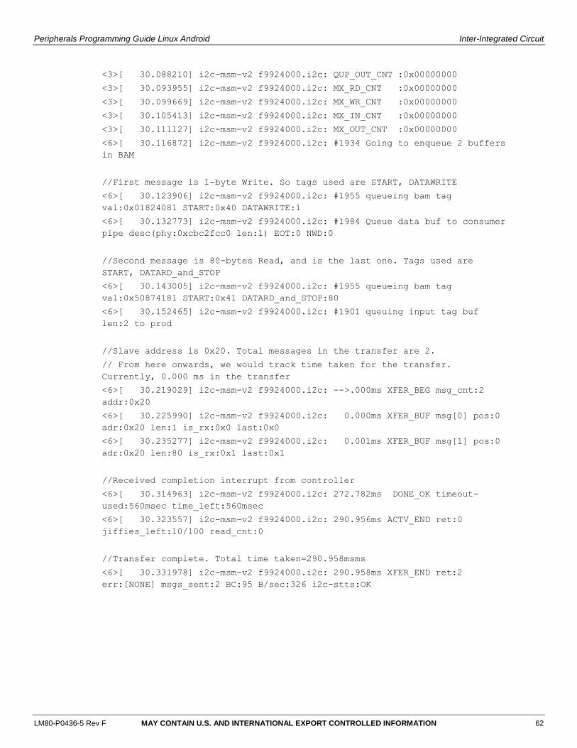
Peripherals Programming Guide Linux Android Inter-Integrated Circuit
LM80-P0436-5 Rev F MAY CONTAIN U.S. AND INTERNATIONAL EXPORT CONTROLLED INFORMATION 62
<3>[ 30.088210] i2c-msm-v2 f9924000.i2c: QUP_OUT_CNT :0x00000000
<3>[ 30.093955] i2c-msm-v2 f9924000.i2c: MX_RD_CNT :0x00000000
<3>[ 30.099669] i2c-msm-v2 f9924000.i2c: MX_WR_CNT :0x00000000
<3>[ 30.105413] i2c-msm-v2 f9924000.i2c: MX_IN_CNT :0x00000000
<3>[ 30.111127] i2c-msm-v2 f9924000.i2c: MX_OUT_CNT :0x00000000
<6>[ 30.116872] i2c-msm-v2 f9924000.i2c: #1934 Going to enqueue 2 buffers
in BAM
//First message is 1-byte Write. So tags used are START, DATAWRITE
<6>[ 30.123906] i2c-msm-v2 f9924000.i2c: #1955 queueing bam tag
val:0x01824081 START:0x40 DATAWRITE:1
<6>[ 30.132773] i2c-msm-v2 f9924000.i2c: #1984 Queue data buf to consumer
pipe desc(phy:0xcbc2fcc0 len:1) EOT:0 NWD:0
//Second message is 80-bytes Read, and is the last one. Tags used are
START, DATARD_and_STOP
<6>[ 30.143005] i2c-msm-v2 f9924000.i2c: #1955 queueing bam tag
val:0x50874181 START:0x41 DATARD_and_STOP:80
<6>[ 30.152465] i2c-msm-v2 f9924000.i2c: #1901 queuing input tag buf
len:2 to prod
//Slave address is 0x20. Total messages in the transfer are 2.
// From here onwards, we would track time taken for the transfer.
Currently, 0.000 ms in the transfer
<6>[ 30.219029] i2c-msm-v2 f9924000.i2c: -->.000ms XFER_BEG msg_cnt:2
addr:0x20
<6>[ 30.225990] i2c-msm-v2 f9924000.i2c: 0.000ms XFER_BUF msg[0] pos:0
adr:0x20 len:1 is_rx:0x0 last:0x0
<6>[ 30.235277] i2c-msm-v2 f9924000.i2c: 0.001ms XFER_BUF msg[1] pos:0
adr:0x20 len:80 is_rx:0x1 last:0x1
//Received completion interrupt from controller
<6>[ 30.314963] i2c-msm-v2 f9924000.i2c: 272.782ms DONE_OK timeout-
used:560msec time_left:560msec
<6>[ 30.323557] i2c-msm-v2 f9924000.i2c: 290.956ms ACTV_END ret:0
jiffies_left:10/100 read_cnt:0
//Transfer complete. Total time taken=290.958msms
<6>[ 30.331978] i2c-msm-v2 f9924000.i2c: 290.958ms XFER_END ret:2
err:[NONE] msgs_sent:2 BC:95 B/sec:326 i2c-stts:OK
LM80-P0436-5 Rev F MAY CONTAIN U.S. AND INTERNATIONAL EXPORT CONTROLLED INFORMATION 63
5 Serial Peripheral Interface
This chapter describes the SPI and explains how to configure it in the kernel.
5.1 Hardware overview
For a BLSP overview, see Section 3.1.
For a QUP overview, see Section 4.1.1.
5.1.1 SPI core
The SPI allows full-/half-duplex, synchronous, serial communication between a master and slave.
There is no explicit communication framing, error checking, or defined data word length. Hence,
the communication is strictly at the raw bit level.
5.1.1.1 Key features
Supports up to 50 MHz
Supports 4 to 32 bits per word of transfer
Supports a maximum of four Chip Selects (CSes) per bus
Supports BAM
5.1.2 QUP SPI parameters
To match the labeling in the software interface manual, each QUP is identified by a BLSP core
and a QUP core (0 to 5). In hardware design documents, BLSPs are identified as BLSP[1:12].
MSM8916 and APQ8016E chipsets contain a single BLSP core.
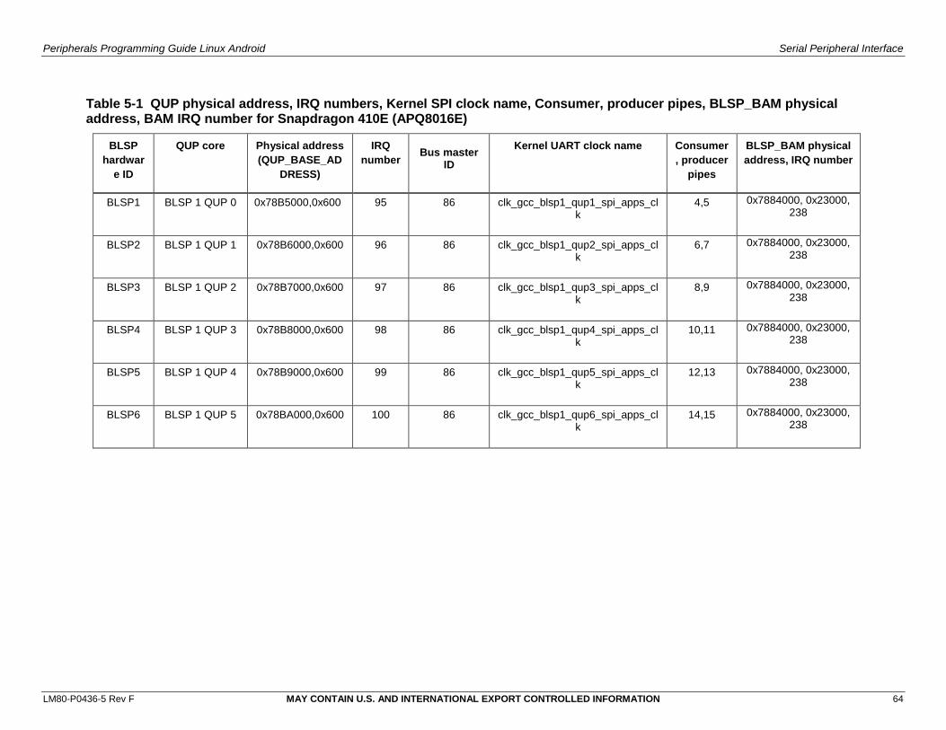
Peripherals Programming Guide Linux Android Serial Peripheral Interface
LM80-P0436-5 Rev F MAY CONTAIN U.S. AND INTERNATIONAL EXPORT CONTROLLED INFORMATION 64
Table 5-1 QUP physical address, IRQ numbers, Kernel SPI clock name, Consumer, producer pipes, BLSP_BAM physical address, BAM IRQ number for Snapdragon 410E (APQ8016E)
BLSP
hardwar
e ID
QUP core Physical address
(QUP_BASE_AD
DRESS)
IRQ
number
Bus master
ID
Kernel UART clock name Consumer
, producer
pipes
BLSP_BAM physical
address, IRQ number
BLSP1 BLSP 1 QUP 0 0x78B5000,0x600 95 86 clk_gcc_blsp1_qup1_spi_apps_clk
4,5 0x7884000, 0x23000, 238
BLSP2 BLSP 1 QUP 1 0x78B6000,0x600 96 86 clk_gcc_blsp1_qup2_spi_apps_clk
6,7 0x7884000, 0x23000, 238
BLSP3 BLSP 1 QUP 2 0x78B7000,0x600 97 86 clk_gcc_blsp1_qup3_spi_apps_clk
8,9 0x7884000, 0x23000, 238
BLSP4 BLSP 1 QUP 3 0x78B8000,0x600 98 86 clk_gcc_blsp1_qup4_spi_apps_clk
10,11 0x7884000, 0x23000, 238
BLSP5 BLSP 1 QUP 4 0x78B9000,0x600 99 86 clk_gcc_blsp1_qup5_spi_apps_clk
12,13 0x7884000, 0x23000, 238
BLSP6 BLSP 1 QUP 5 0x78BA000,0x600 100 86 clk_gcc_blsp1_qup6_spi_apps_clk
14,15 0x7884000, 0x23000, 238
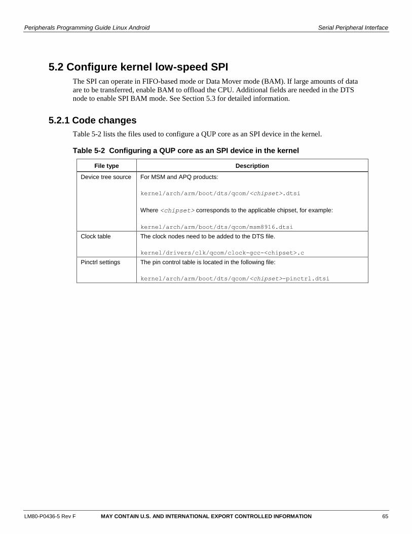
Peripherals Programming Guide Linux Android Serial Peripheral Interface
LM80-P0436-5 Rev F MAY CONTAIN U.S. AND INTERNATIONAL EXPORT CONTROLLED INFORMATION 65
5.2 Configure kernel low-speed SPI
The SPI can operate in FIFO-based mode or Data Mover mode (BAM). If large amounts of data
are to be transferred, enable BAM to offload the CPU. Additional fields are needed in the DTS
node to enable SPI BAM mode. See Section 5.3 for detailed information.
5.2.1 Code changes
Table 5-2 lists the files used to configure a QUP core as an SPI device in the kernel.
Table 5-2 Configuring a QUP core as an SPI device in the kernel
File type Description
Device tree source For MSM and APQ products:
kernel/arch/arm/boot/dts/qcom/<chipset>.dtsi
Where <chipset> corresponds to the applicable chipset, for example:
kernel/arch/arm/boot/dts/qcom/msm8916.dtsi
Clock table The clock nodes need to be added to the DTS file.
kernel/drivers/clk/qcom/clock-gcc-<chipset>.c
Pinctrl settings The pin control table is located in the following file:
kernel/arch/arm/boot/dts/qcom/<chipset>-pinctrl.dtsi
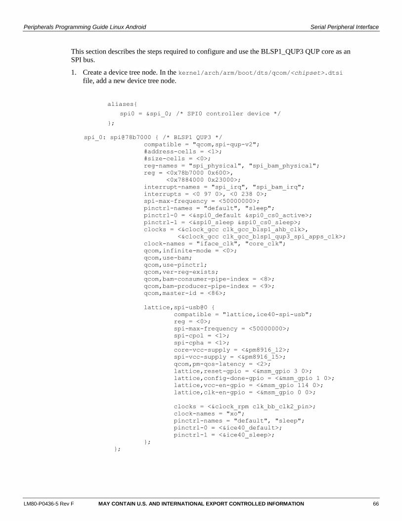
Peripherals Programming Guide Linux Android Serial Peripheral Interface
LM80-P0436-5 Rev F MAY CONTAIN U.S. AND INTERNATIONAL EXPORT CONTROLLED INFORMATION 66
This section describes the steps required to configure and use the BLSP1_QUP3 QUP core as an
SPI bus.
1. Create a device tree node. In the kernel/arch/arm/boot/dts/qcom/<chipset>.dtsi
file, add a new device tree node.
aliases{
spi0 = &spi_0; /* SPI0 controller device */
};
spi_0: spi@78b7000 { /* BLSP1 QUP3 */
compatible = "qcom,spi-qup-v2";
#address-cells = <1>;
#size-cells = <0>;
reg-names = "spi_physical", "spi_bam_physical";
reg = <0x78b7000 0x600>,
<0x7884000 0x23000>;
interrupt-names = "spi_irq", "spi_bam_irq";
interrupts = <0 97 0>, <0 238 0>;
spi-max-frequency = <50000000>;
pinctrl-names = "default", "sleep";
pinctrl-0 = <&spi0_default &spi0_cs0_active>;
pinctrl-1 = <&spi0_sleep &spi0_cs0_sleep>;
clocks = <&clock_gcc clk_gcc_blsp1_ahb_clk>,
<&clock_gcc clk_gcc_blsp1_qup3_spi_apps_clk>;
clock-names = "iface_clk", "core_clk";
qcom,infinite-mode = <0>;
qcom,use-bam;
qcom,use-pinctrl;
qcom,ver-reg-exists;
qcom,bam-consumer-pipe-index = <8>;
qcom,bam-producer-pipe-index = <9>;
qcom,master-id = <86>;
lattice,spi-usb@0 {
compatible = "lattice,ice40-spi-usb";
reg = <0>;
spi-max-frequency = <50000000>;
spi-cpol = <1>;
spi-cpha = <1>;
core-vcc-supply = <&pm8916_l2>;
spi-vcc-supply = <&pm8916_l5>;
qcom,pm-qos-latency = <2>;
lattice,reset-gpio = <&msm_gpio 3 0>;
lattice,config-done-gpio = <&msm_gpio 1 0>;
lattice,vcc-en-gpio = <&msm_gpio 114 0>;
lattice,clk-en-gpio = <&msm_gpio 0 0>;
clocks = <&clock_rpm clk_bb_clk2_pin>;
clock-names = "xo";
pinctrl-names = "default", "sleep";
pinctrl-0 = <&ice40_default>;
pinctrl-1 = <&ice40_sleep>;
};
};
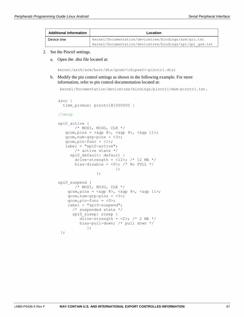
Peripherals Programming Guide Linux Android Serial Peripheral Interface
LM80-P0436-5 Rev F MAY CONTAIN U.S. AND INTERNATIONAL EXPORT CONTROLLED INFORMATION 67
Additional information Location
Device tree kernel/Documentation/devicetree/bindings/arm/gic.txt
kernel/Documentation/devicetree/bindings/spi/spi_qsd.txt
2. Set the Pinctrl settings.
a. Open the .dtsi file located at:
kernel/arch/arm/boot/dts/qcom/<chipset>-pinctrl.dtsi
b. Modify the pin control settings as shown in the following example. For more
information, refer to pin control documentation located at:
kernel/Documentation/devicetree/bindings/pinctrl/msm-pinctrl.txt.
&soc {
tlmm_pinmux: pinctrl@1000000 {
//snip
spi0_active {
/* MOSI, MISO, CLK */
qcom,pins = <&gp 8>, <&gp 9>, <&gp 11>;
qcom,num-grp-pins = <3>;
qcom,pin-func = <1>;
label = "spi0-active";
/* active state */
spi0_default: default {
drive-strength = <12>; /* 12 MA */
bias-disable = <0>; /* No PULL */
};
};
spi0_suspend {
/* MOSI, MISO, CLK */
qcom,pins = <&gp 8>, <&gp 9>, <&gp 11>;
qcom,num-grp-pins = <3>;
qcom,pin-func = <0>;
label = "spi0-suspend";
/* suspended state */
spi0_sleep: sleep {
drive-strength = <2>; /* 2 MA */
bias-pull-down; /* pull down */
};
};
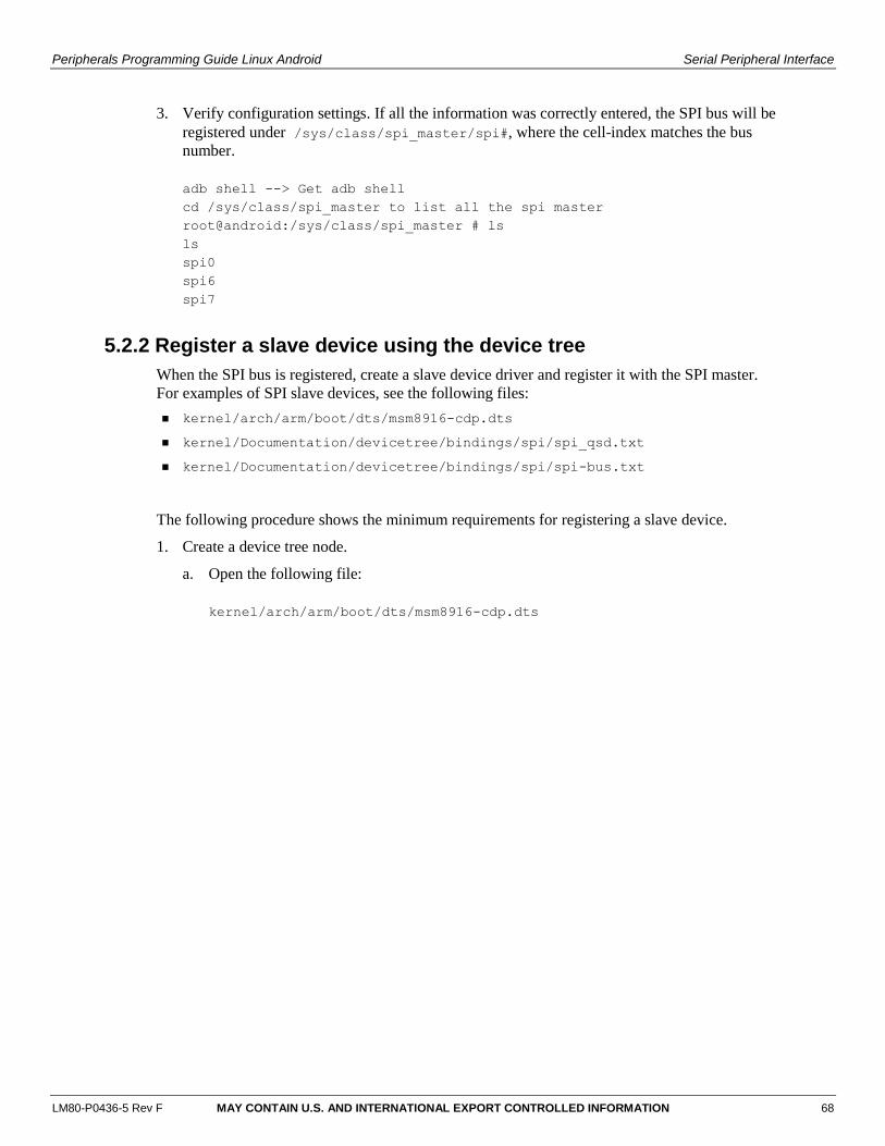
Peripherals Programming Guide Linux Android Serial Peripheral Interface
LM80-P0436-5 Rev F MAY CONTAIN U.S. AND INTERNATIONAL EXPORT CONTROLLED INFORMATION 68
3. Verify configuration settings. If all the information was correctly entered, the SPI bus will be
registered under /sys/class/spi_master/spi#, where the cell-index matches the bus
number.
adb shell --> Get adb shell
cd /sys/class/spi_master to list all the spi master
root@android:/sys/class/spi_master # ls
ls
spi0
spi6
spi7
5.2.2 Register a slave device using the device tree
When the SPI bus is registered, create a slave device driver and register it with the SPI master.
For examples of SPI slave devices, see the following files:
kernel/arch/arm/boot/dts/msm8916-cdp.dts
kernel/Documentation/devicetree/bindings/spi/spi_qsd.txt
kernel/Documentation/devicetree/bindings/spi/spi-bus.txt
The following procedure shows the minimum requirements for registering a slave device.
1. Create a device tree node.
a. Open the following file:
kernel/arch/arm/boot/dts/msm8916-cdp.dts
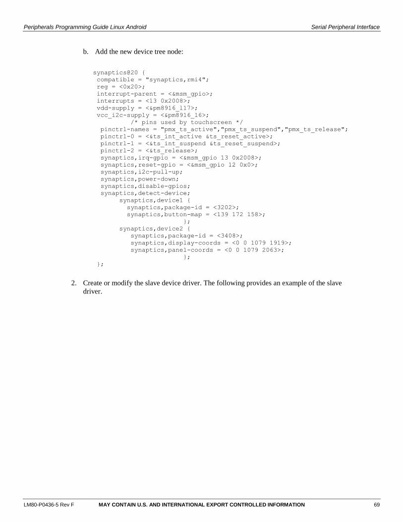
Peripherals Programming Guide Linux Android Serial Peripheral Interface
LM80-P0436-5 Rev F MAY CONTAIN U.S. AND INTERNATIONAL EXPORT CONTROLLED INFORMATION 69
b. Add the new device tree node:
2. Create or modify the slave device driver. The following provides an example of the slave
driver.
synaptics@20 {
compatible = "synaptics,rmi4";
reg = <0x20>;
interrupt-parent = <&msm_gpio>;
interrupts = <13 0x2008>;
vdd-supply = <&pm8916_l17>;
vcc_i2c-supply = <&pm8916_l6>;
/* pins used by touchscreen */
pinctrl-names = "pmx_ts_active","pmx_ts_suspend","pmx_ts_release";
pinctrl-0 = <&ts_int_active &ts_reset_active>;
pinctrl-1 = <&ts_int_suspend &ts_reset_suspend>;
pinctrl-2 = <&ts_release>;
synaptics,irq-gpio = <&msm_gpio 13 0x2008>;
synaptics,reset-gpio = <&msm_gpio 12 0x0>;
synaptics,i2c-pull-up;
synaptics,power-down;
synaptics,disable-gpios;
synaptics,detect-device;
synaptics,device1 {
synaptics,package-id = <3202>;
synaptics,button-map = <139 172 158>;
};
synaptics,device2 {
synaptics,package-id = <3408>;
synaptics,display-coords = <0 0 1079 1919>;
synaptics,panel-coords = <0 0 1079 2063>;
};
};
Peripherals Programming Guide Linux Android Serial Peripheral Interface
LM80-P0436-5 Rev F MAY CONTAIN U.S. AND INTERNATIONAL EXPORT CONTROLLED INFORMATION 70
#include <linux/module.h>
#include <linux/init.h>
#include <linux/delay.h>
#include <linux/spi/spi.h>
#include <linux/interrupt.h>
#include <linux/slab.h>
#include <linux/gpio.h>
#include <linux/debugfs.h>
#include <linux/seq_file.h>
#include <linux/regulator/consumer.h>
#include <linux/string.h>
#include <linux/of_gpio.h>
#ifdef CONFIG_OF //Open firmware must be defined for dts useage
static struct of_device_id qcom_spi_test_table[] = {
{ .compatible = "qcom,spi-test",}, //Compatible node must match
//dts
{ },
};
#else
#define qcom_spi_test_table NULL
#endif
#define BUFFER_SIZE 4<<10
struct spi_message spi_msg;
struct spi_transfer spi_xfer;
u8 *tx_buf; //This needs to be DMA friendly buffer
static int spi_test_transfer(struct spi_device *spi)
{
spi->mode |=SPI_LOOP; //Enable Loopback mode
spi_message_init(&spi_msg);
spi_xfer.tx_buf = tx_buf;
spi_xfer.len = BUFFER_SIZE;
spi_xfer.bits_per_word = 8;
spi_xfer.speed_hz = spi->max_speed_hz;
spi_message_add_tail(&spi_xfer, &spi_msg);
return spi_sync(spi, &spi_msg);
}
static int spi_test_probe(struct spi_device *spi)
{
int irq_gpio = -1;
int irq;
int cs;
int cpha,cpol,cs_high;
u32 max_speed;
dev_err(&spi->dev, "%s\n", __func__);
Peripherals Programming Guide Linux Android Serial Peripheral Interface
LM80-P0436-5 Rev F MAY CONTAIN U.S. AND INTERNATIONAL EXPORT CONTROLLED INFORMATION 71
//allocate memory for transfer
tx_buf = kmalloc(BUFFER_SIZE, GFP_ATOMIC);
if(tx_buf == NULL){
dev_err(&spi->dev, "%s: mem alloc failed\n", __func__);
return -ENOMEM;
}
//Parse data using dt.
if(spi->dev.of_node){
irq_gpio = of_get_named_gpio_flags(spi->dev.of_node,
"qcom_spi_test,irq-gpio", 0, NULL);
}
irq = spi->irq;
cs = spi->chip_select;
cpha = ( spi->mode & SPI_CPHA ) ? 1:0;
cpol = ( spi->mode & SPI_CPOL ) ? 1:0;
cs_high = ( spi->mode & SPI_CS_HIGH ) ? 1:0;
max_speed = spi->max_speed_hz;
dev_err(&spi->dev, "gpio [%d] irq [%d] gpio_irq [%d] cs [%x] CPHA
[%x] CPOL [%x] CS_HIGH [%x]\n",
irq_gpio, irq, gpio_to_irq(irq_gpio), cs, cpha, cpol,
cs_high);
dev_err(&spi->dev, "Max_speed [%d]\n", max_speed );
//Transfer can be done after spi_device structure is created
spi->bits_per_word = 8;
dev_err(&spi->dev, "SPI sync returned [%d]\n",
spi_test_transfer(spi));
return 0;
}
//SPI Driver Info
static struct spi_driver spi_test_driver = {
.driver = {
.name = "qcom_spi_test",
.owner = THIS_MODULE,
.of_match_table = qcom_spi_test_table,
},
.probe = spi_test_probe,
};
static int __init spi_test_init(void)
{
return spi_register_driver(&spi_test_driver);
}
static void __exit spi_test_exit(void)
{
spi_unregister_driver(&spi_test_driver);
}
module_init(spi_test_init);
module_exit(spi_test_exit);
MODULE_DESCRIPTION("SPI TEST");
MODULE_LICENSE("GPL v2");
Peripherals Programming Guide Linux Android Serial Peripheral Interface
LM80-P0436-5 Rev F MAY CONTAIN U.S. AND INTERNATIONAL EXPORT CONTROLLED INFORMATION 72
3. Verify that the device tree was configured. In the kernel log, the following message indicates
the device tree was successfully configured.
<3>[ 2.503571] qcom_spi_test spi6.0: spi_test_probe
<3>[ 2.507305] qcom_spi_test spi6.0: gpio [61] irq [306] gpio_irq
[306]
cs [0] CPHA [1] CPOL [1] CS_HIGH [1]
<3>[ 2.516825] qcom_spi_test spi6.0: Max_speed [4800000]
<3>[ 2.521932] qcom_spi_test spi6.0: SPI sync returned [0]
5.3 Configure kernel high-speed SPI
The SPI can operate in Data Mover mode (BAM) or FIFO-based mode. If large amounts of data
are to be transferred, enable BAM to offload the CPU. For BLSP BAM registers and IRQs, see
Table 5-1.
5.3.1 Code changes
The following describes how to enable BAM (Data Mover mode) in the SPI.
1. Modify the device tree. The following example shows the additional fields needed in the DTS
node to enable SPI BAM mode. See Section 5.2 for more information on the field needed in
the DTS node.
spi_0: spi@78b7000 { /* BLSP1 QUP3 */
compatible = "qcom,spi-qup-v2";
#address-cells = <1>;
#size-cells = <0>;
reg-names = "spi_physical", "spi_bam_physical";
reg = <0x78b7000 0x600>,
<0x7884000 0x23000>;
interrupt-names = "spi_irq", "spi_bam_irq";
interrupts = <0 97 0>, <0 238 0>;
spi-max-frequency = <50000000>;
pinctrl-names = "default", "sleep";
pinctrl-0 = <&spi0_default &spi0_cs0_active>;
pinctrl-1 = <&spi0_sleep &spi0_cs0_sleep>;
clocks = <&clock_gcc clk_gcc_blsp1_ahb_clk>,
<&clock_gcc clk_gcc_blsp1_qup3_spi_apps_clk>;
clock-names = "iface_clk", "core_clk";
qcom,infinite-mode = <0>;
qcom,use-bam;
qcom,use-pinctrl;
qcom,ver-reg-exists;
qcom,bam-consumer-pipe-index = <8>;
qcom,bam-producer-pipe-index = <9>;
qcom,master-id = <86>;
};
Peripherals Programming Guide Linux Android Serial Peripheral Interface
LM80-P0436-5 Rev F MAY CONTAIN U.S. AND INTERNATIONAL EXPORT CONTROLLED INFORMATION 73
Additional information:
kernel/Documentation/devicetree/bindings/arm/gic.txt
kernel/Documentation/devicetree/bindings/spi/spi_qsd.txt
For information on BAM pipes, see Table 5-1.
5.4 SPI power management
SPI slave devices must register system suspend and resume (SYSTEM_PM_OPS) handlers with
the power management framework to ensure that no SPI transactions are initiated after the SPI
master is suspended. For examples, see Section 4.4.
5.5 Code walkthrough
5.5.1 Probing
5.5.1.1 Call the SPI master probe
Similar to the UART probe, the SPI master probe is called with the following call stack (see
3.5.1).
-000|msm_spi_probe()
-001|platform_drv_probe()
-002|driver_probe_device()
-003|__driver_attach()
-004|bus_for_each_dev()
-005|bus_add_driver()
-006|driver_register()
-007|platform_driver_probe()
-008|do_one_initcall()
Table 5-3 lists resources that must be defined for a successful SPI master registration.
Table 5-3 SPI master registration resources required for BAM
Resource Description
msm_spi_dt_to_pdata-->
msm_spi_dt_to_pdata_populate()
Parses the device tree
msm_spi_bam_get_resources Gets BAM informations
msm_spi_request_irq Gets IRQ information
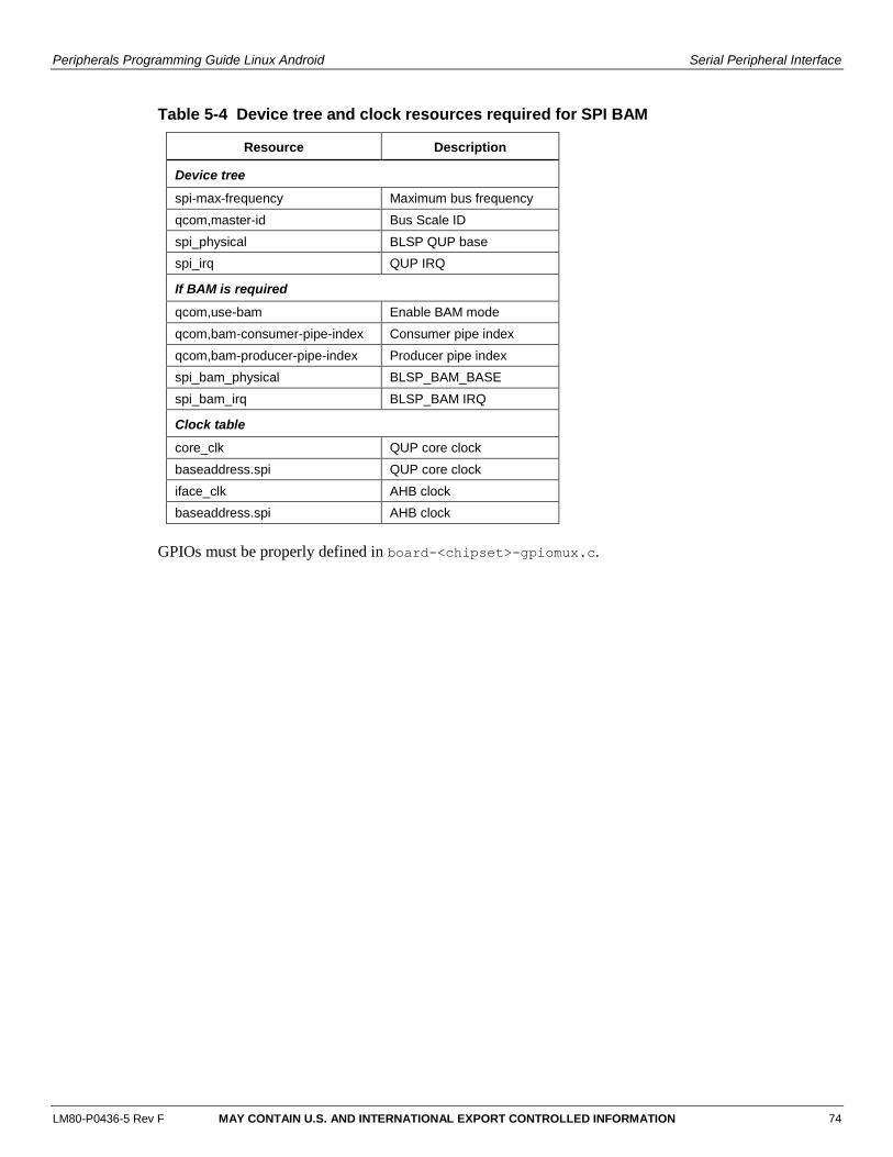
Peripherals Programming Guide Linux Android Serial Peripheral Interface
LM80-P0436-5 Rev F MAY CONTAIN U.S. AND INTERNATIONAL EXPORT CONTROLLED INFORMATION 74
Table 5-4 Device tree and clock resources required for SPI BAM
Resource Description
Device tree
spi-max-frequency Maximum bus frequency
qcom,master-id Bus Scale ID
spi_physical BLSP QUP base
spi_irq QUP IRQ
If BAM is required
qcom,use-bam Enable BAM mode
qcom,bam-consumer-pipe-index Consumer pipe index
qcom,bam-producer-pipe-index Producer pipe index
spi_bam_physical BLSP_BAM_BASE
spi_bam_irq BLSP_BAM IRQ
Clock table
core_clk QUP core clock
baseaddress.spi QUP core clock
iface_clk AHB clock
baseaddress.spi AHB clock
GPIOs must be properly defined in board-<chipset>-gpiomux.c.
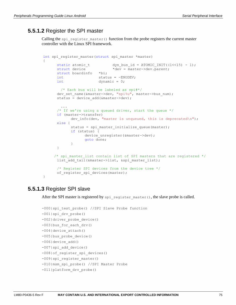
Peripherals Programming Guide Linux Android Serial Peripheral Interface
LM80-P0436-5 Rev F MAY CONTAIN U.S. AND INTERNATIONAL EXPORT CONTROLLED INFORMATION 75
5.5.1.2 Register the SPI master
Calling the spi_register_master() function from the probe registers the current master
controller with the Linux SPI framework.
5.5.1.3 Register SPI slave
After the SPI master is registered by spi_register_master(), the slave probe is called.
-000|spi_test_probe() //SPI Slave Probe function
-001|spi_drv_probe()
-002|driver_probe_device()
-003|bus_for_each_drv()
-004|device_attach()
-005|bus_probe_device()
-006|device_add()
-007|spi_add_device()
-008|of_register_spi_devices()
-009|spi_register_master()
-010|msm_spi_probe() //SPI Master Probe
-011|platform_drv_probe()
int spi_register_master(struct spi_master *master)
{
static atomic_t dyn_bus_id = ATOMIC_INIT((1<<15) - 1);
struct device *dev = master->dev.parent;
struct boardinfo *bi;
int status = -ENODEV;
int dynamic = 0;
/* Each bus will be labeled as spi#*/
dev_set_name(&master->dev, "spi%u", master->bus_num);
status = device_add(&master->dev);
...
/* If we're using a queued driver, start the queue */
if (master->transfer)
dev_info(dev, "master is unqueued, this is deprecated\n");
else {
status = spi_master_initialize_queue(master);
if (status) {
device_unregister(&master->dev);
goto done;
}
}
/* spi_master_list contain list of SPI masters that are registered */
list_add_tail(&master->list, &spi_master_list);
/* Register SPI devices from the device tree */
of_register_spi_devices(master);
}
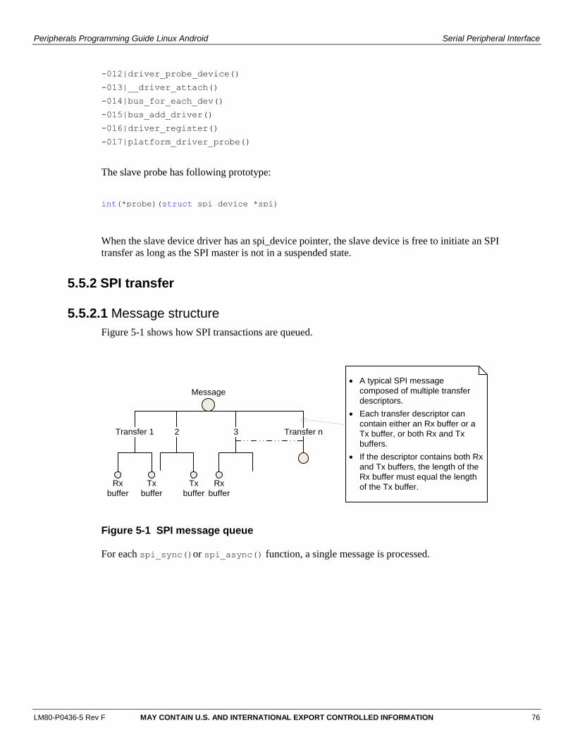
Peripherals Programming Guide Linux Android Serial Peripheral Interface
LM80-P0436-5 Rev F MAY CONTAIN U.S. AND INTERNATIONAL EXPORT CONTROLLED INFORMATION 76
-012|driver_probe_device()
-013|__driver_attach()
-014|bus_for_each_dev()
-015|bus_add_driver()
-016|driver_register()
-017|platform_driver_probe()
The slave probe has following prototype:
When the slave device driver has an spi_device pointer, the slave device is free to initiate an SPI
transfer as long as the SPI master is not in a suspended state.
5.5.2 SPI transfer
5.5.2.1 Message structure
Figure 5-1 shows how SPI transactions are queued.
Message
Rx
buffer
Tx
buffer
Tx
buffer
Rx
buffer
Transfer 1 Transfer n32
A typical SPI message
composed of multiple transfer
descriptors.
Each transfer descriptor can
contain either an Rx buffer or a
Tx buffer, or both Rx and Tx
buffers.
If the descriptor contains both Rx
and Tx buffers, the length of the
Rx buffer must equal the length
of the Tx buffer.
Figure 5-1 SPI message queue
For each spi_sync()or spi_async() function, a single message is processed.
int(*probe)(struct spi_device *spi)
Peripherals Programming Guide Linux Android Serial Peripheral Interface
LM80-P0436-5 Rev F MAY CONTAIN U.S. AND INTERNATIONAL EXPORT CONTROLLED INFORMATION 77
5.5.2.2 spi_sync()
The spi_sync() function is a blocking call that waits until an entire message is transferred
before returning to the caller.
5.5.2.3 spi_async()
The spi_async() function is a nonblocking call that can be called from an atomic context also.
With this function, a slave device can queue multiple messages and wait for the master to call
back. For each message that is complete, the master calls the callback.
int spi_sync(struct spi_device *spi, struct spi_message *message,
)
{
DECLARE_COMPLETION_ONSTACK(done);
int status;
struct spi_master *master = spi->master;
/* Initialize the completion call back */
message->complete = spi_complete;
message->context = &done;
/* Queue the message */
status = spi_async_locked(spi, message);
/* Wait for completion signal from master */
if (status == 0) {
wait_for_completion(&done);
status = message->status;
}
return status;
}
static int spi_async(struct spi_device *spi, struct spi_message *message)
{
struct spi_master *master = spi->master;
message->spi = spi;
message->status = -EINPROGRESS;
/* Queue the Transfer with the SPI Master */
return master->transfer(spi, message);
}
LM80-P0436-5 Rev F MAY CONTAIN U.S. AND INTERNATIONAL EXPORT CONTROLLED INFORMATION 78
6 BLSP BAM
This chapter describes the Bus Access Manager (BAM) software architecture relevant to the
BLSP.
6.1 Source code
The kernel/arch/arm/mach-msm/include/mach/sps.h header file contains all of the
functions, flags and data structures that are exposed to client drivers.
The source directory is kernel/drivers/platform/msm/sps/.
6.2 Key functions
6.2.1 sps_phy2h()
This function checks the registered BAM device list, sps->bam_q, to see if a physical address
of the BAM is already registered. If a BAM address is registered, this function returns the BAM
handler, struct sps_bam.
6.2.2 sps_register_bam_device()
If the BAM device is not already registered, this function registers it with the BAM driver.
Initializes the sps_bam structure by calling sps_bam_device_init()
Adds the sps_bam structure to the sps->bam_q list
Returns the handler for the sps_bam structure
6.2.3 sps_alloc_endpoint()
This function allocates the sps_pipe structure and returns the handler after initializing it by calling
sps_client_init().
Sets sps_pipe.client_state to SPS_STATE_DISCONNECT
Sets sps_pipe.connect to SPSRM_CLEAR
Peripherals Programming Guide Linux Android BLSP BAM
LM80-P0436-5 Rev F MAY CONTAIN U.S. AND INTERNATIONAL EXPORT CONTROLLED INFORMATION 79
6.2.4 sps_connect()
This function initializes the BAM hardware and estabishes communication between the BAM and
processor.
Copies the sps_connect structure to sps_pipe.connect
Allocates the sps_connection structure and maps it to sps_pipe
Configures and enables the BAM pipe
Sets a connection from sps_pipe.client_state to SPS_STATE_CONNECT
6.2.5 sps_register_event()
This function registers an event handler for the sps_event by updating sps_pipe.event_regs.
6.2.6 sps_transfer_one()
This function queues a single descriptor into the BAM pipe by calling
sps_bam_pipe_transfer_one.
Updates sps_pipe.sys.desc_offset to the next location
PIPE_EVENT_REG = "next_write"
6.2.7 bam_isr()
This function is the ISR handler for the BLSP BAM.
Determines which pipe caused an interrupt by reading the BAM_IRQ_SRCS register
Calls pipe_handler-->pipe_handler_eot to process the interrupt
Updates sps_pipe.sys.acked_offset with SW_DESC_OFST
Call stack:
-000|client_callback()
-001|trigger_event.isra.1()
-002|pipe_handler_eot()
-003|pipe_handler()
-004|bam_isr()
-005|handle_irq_event_percpu()
-006|handle_irq_event()
-007|handle_fasteoi_irq()
-008|generic_handle_irq()
-009|handle_IRQ()
-010|gic_handle_irq()
6.2.8 sps_disconnect()
This function disables the BAM hardware connection and deallocates any resources allocated by
the SPS driver.
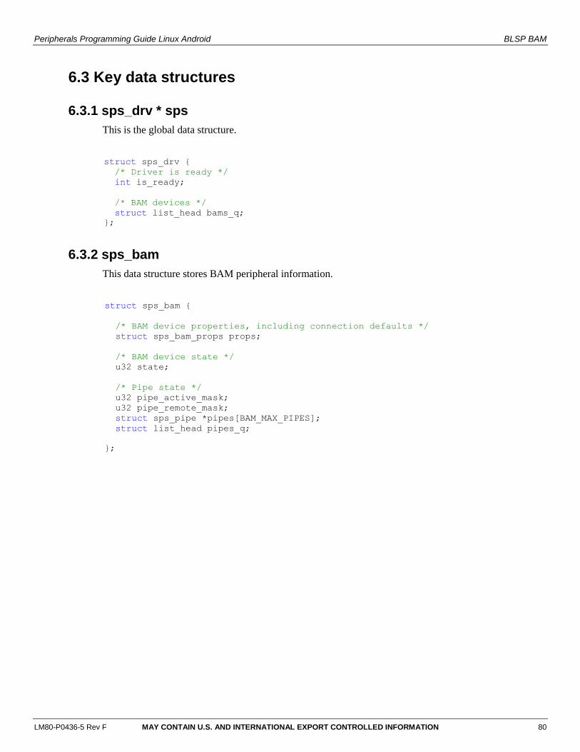
Peripherals Programming Guide Linux Android BLSP BAM
LM80-P0436-5 Rev F MAY CONTAIN U.S. AND INTERNATIONAL EXPORT CONTROLLED INFORMATION 80
6.3 Key data structures
6.3.1 sps_drv * sps
This is the global data structure.
6.3.2 sps_bam
This data structure stores BAM peripheral information.
struct sps_drv {
/* Driver is ready */
int is_ready;
/* BAM devices */
struct list_head bams_q;
};
struct sps_bam {
/* BAM device properties, including connection defaults */
struct sps_bam_props props;
/* BAM device state */
u32 state;
/* Pipe state */
u32 pipe_active_mask;
u32 pipe_remote_mask;
struct sps_pipe *pipes[BAM_MAX_PIPES];
struct list_head pipes_q;
};
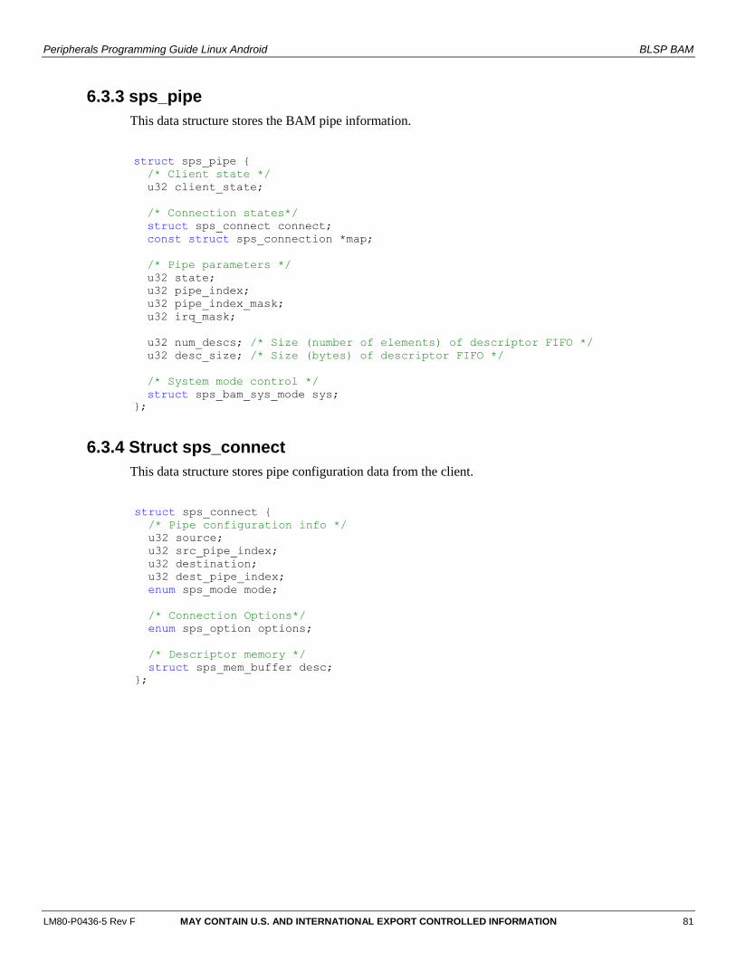
Peripherals Programming Guide Linux Android BLSP BAM
LM80-P0436-5 Rev F MAY CONTAIN U.S. AND INTERNATIONAL EXPORT CONTROLLED INFORMATION 81
6.3.3 sps_pipe
This data structure stores the BAM pipe information.
6.3.4 Struct sps_connect
This data structure stores pipe configuration data from the client.
struct sps_pipe {
/* Client state */
u32 client_state;
/* Connection states*/
struct sps_connect connect;
const struct sps_connection *map;
/* Pipe parameters */
u32 state;
u32 pipe_index;
u32 pipe_index_mask;
u32 irq_mask;
u32 num_descs; /* Size (number of elements) of descriptor FIFO */
u32 desc_size; /* Size (bytes) of descriptor FIFO */
/* System mode control */
struct sps_bam_sys_mode sys;
};
struct sps_connect {
/* Pipe configuration info */
u32 source;
u32 src_pipe_index;
u32 destination;
u32 dest_pipe_index;
enum sps_mode mode;
/* Connection Options*/
enum sps_option options;
/* Descriptor memory */
struct sps_mem_buffer desc;
};
Peripherals Programming Guide Linux Android BLSP BAM
LM80-P0436-5 Rev F MAY CONTAIN U.S. AND INTERNATIONAL EXPORT CONTROLLED INFORMATION 82
6.3.5 sps_register_event
This data structure stores information with respect to the event handler.
6.3.6 sps_bam_sys_mode
This data structure stores descriptor buffer information and event offsets.
struct sps_register_event {
/* Options that will trigger */
enum sps_option options;
enum sps_trigger mode;
/* Handler or completion signal */
struct completion *xfer_done;
void (*callback)(struct sps_event_notify *notify);
void *user;
};
struct sps_bam_sys_mode {
/* Descriptor FIFO control */
u8 *desc_buf; /* Descriptor FIFO for BAM pipe */
u32 desc_offset; /* Next new descriptor to be written to hardware */
u32 acked_offset; /* Next descriptor to be retired by software */
/* Descriptor cache control (!no_queue only) */
u8 *desc_cache; /* Software cache of descriptor FIFO contents */
u32 cache_offset; /* Next descriptor to be cached (ack_xfers only) */
};
LM80-P0436-5 Rev F MAY CONTAIN U.S. AND INTERNATIONAL EXPORT CONTROLLED INFORMATION 83
7 GPIO
Each MSM/MDM/APQ chipset has a dedicated number of GPIOs that can be configured for
multiple functions. For example, if you check the GPIO mapping for MSM8916 GPIO 0, you will
see that the GPIO can be configured as one of the following functions at any time:
Function 0 – GPIO
Function 1 – BLSP1 SPI MOSI
Function 2 – BLSP1 UART TX
Function 3 – BLSP1 User Identity Module (UIM) data
Function 4 – HDMI_RCV_DET
7.1 Critical registers
This section describes some critical hardware registers that are important for debugging.
7.1.1 GPIO_CFGn
GPIO_CFGn controls the GPIO properties, such as Output Enable, Drive Strength, Pull, and
GPIO Function Select.
For example, for MSM8916:
Physical Address: 0x01000000 + (0x1000 * n) = GPIO_CFGn
n = GPIO #
Example Address:
0x01000000 = GPIO_CFG0
0x01001000 = GPIO_CFG1
Bit definition for GPIO_CFGn
Bits 31:11 Reserved
Bit 10 GPIO_HIHYS_EN Control the hihys_EN for GPIO
Bit 9 GPIO_OE Controls the Output Enable for GPIO
when in GPIO mode.
Bits 8:6 DRV_STRENGTH Control Drive Strength
000:2mA 001:4mA 010:6mA 011:8mA
100:10mA 101:12mA 110:14mA 111:16mA
Bits 5:2 FUNC_SEL Make sure Function is GSBI
Check Device Pinout for Correct Function
Peripherals Programming Guide Linux Android GPIO
LM80-P0436-5 Rev F MAY CONTAIN U.S. AND INTERNATIONAL EXPORT CONTROLLED INFORMATION 84
Bits 1:0 GPIO_PULL Internal Pull Configuration
00:No Pull 01: Pull Down
10:Keeper 11: Pull Up
7.1.2 GPIO_IN_OUTn
GPIO_IN_OUTn controls the output value or reads the current GPIO value.
Physical Address: 0x01000004 + (0x1000 * n) = GPIO_IN_OUTn
n = GPIO #
Example Address:
0x01000004 = GPIO_IN_OUT0
0x01001004 = GPIO_IN_OUT1
Bit definition for GPIO_CFGn
Bits 31:2 Reserved
Bit 1 GPIO_OUT Control value of the GPIO Output
Bit 0 GPIO_IN Allow you to read the Input value of the
GPIO
7.1.3 GPIO_INTR_CFGn
GPIO_INTR_CFGn controls the GPIO interrupt configuration settings.
Physical Address: 0x01000008 + (0x1000 * n) = GPIO_INTR_CFGn
n = GPIO #
Example Address:
0x01000008 = GPIO_INTR_CFG0
0x01001008 = GPIO_INTR_CFG1
Bit definition for GPIO_CFGn
Bits 31:9 Reserved
Bit 8 DIR_CONN_IN Being used as Direct Connect Interrupt.
0: Default direct connect
1: Enable Direct connect
Bits 7:5 TARGET_PROC Determine which processor a summary
interrupt should get routed to.
0x4: Apps Summary Interrupt
Bit 4 INTR_RAW_STATUS_EN Enable the RAW status for summary
interrupt.
0: Disable
1: Enable
Bits 3:2 INTR_DECT_CTL Control the Edge or Level Detection
0x0: LEVEL sensitive
0x1: Positive Edge
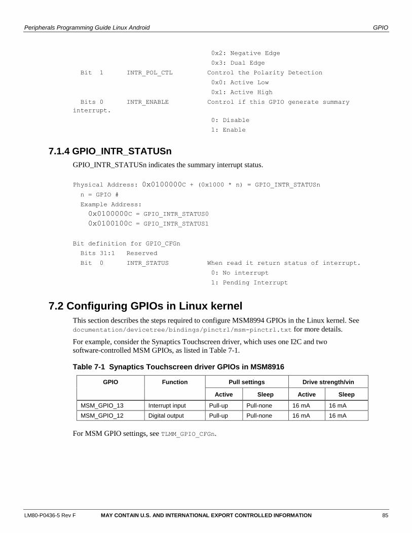
Peripherals Programming Guide Linux Android GPIO
LM80-P0436-5 Rev F MAY CONTAIN U.S. AND INTERNATIONAL EXPORT CONTROLLED INFORMATION 85
0x2: Negative Edge
0x3: Dual Edge
Bit 1 INTR_POL_CTL Control the Polarity Detection
0x0: Active Low
0x1: Active High
Bits 0 INTR_ENABLE Control if this GPIO generate summary
interrupt.
0: Disable
1: Enable
7.1.4 GPIO_INTR_STATUSn
GPIO_INTR_STATUSn indicates the summary interrupt status.
Physical Address: 0x0100000C + (0x1000 * n) = GPIO_INTR_STATUSn
n = GPIO #
Example Address:
0x0100000C = GPIO_INTR_STATUS0
0x0100100C = GPIO_INTR_STATUS1
Bit definition for GPIO_CFGn
Bits 31:1 Reserved
Bit 0 INTR_STATUS When read it return status of interrupt.
0: No interrupt
1: Pending Interrupt
7.2 Configuring GPIOs in Linux kernel
This section describes the steps required to configure MSM8994 GPIOs in the Linux kernel. See
documentation/devicetree/bindings/pinctrl/msm-pinctrl.txt for more details.
For example, consider the Synaptics Touchscreen driver, which uses one I2C and two
software-controlled MSM GPIOs, as listed in Table 7-1.
Table 7-1 Synaptics Touchscreen driver GPIOs in MSM8916
GPIO Function Pull settings Drive strength/vin
Active Sleep Active Sleep
MSM_GPIO_13 Interrupt input Pull-up Pull-none 16 mA 16 mA
MSM_GPIO_12 Digital output Pull-up Pull-none 16 mA 16 mA
For MSM GPIO settings, see TLMM_GPIO_CFGn.
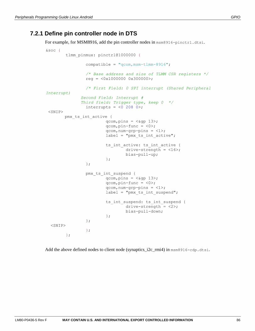
Peripherals Programming Guide Linux Android GPIO
LM80-P0436-5 Rev F MAY CONTAIN U.S. AND INTERNATIONAL EXPORT CONTROLLED INFORMATION 86
7.2.1 Define pin controller node in DTS
For example, for MSM8916, add the pin controller nodes in msm8916-pinctrl.dtsi.
Add the above defined nodes to client node (synaptics_i2c_rmi4) in msm8916-cdp.dtsi.
&soc {
tlmm_pinmux: pinctrl@1000000 {
compatible = "qcom,msm-tlmm-8916";
/* Base address and size of TLMM CSR registers */
reg = <0x1000000 0x300000>;
/* First Field: 0 SPI interrupt (Shared Peripheral
Interrupt)
Second Field: Interrupt #
Third field: Trigger type, keep 0 */
interrupts = <0 208 0>;
<SNIP>
pmx_ts_int_active {
qcom,pins = <&gp 13>;
qcom,pin-func = <0>;
qcom,num-grp-pins = <1>;
label = "pmx_ts_int_active";
ts_int_active: ts_int_active {
drive-strength = <16>;
bias-pull-up;
};
};
pmx_ts_int_suspend {
qcom,pins = <&gp 13>;
qcom,pin-func = <0>;
qcom,num-grp-pins = <1>;
label = "pmx_ts_int_suspend";
ts_int_suspend: ts_int_suspend {
drive-strength = <2>;
bias-pull-down;
};
};
<SNIP>
};
};
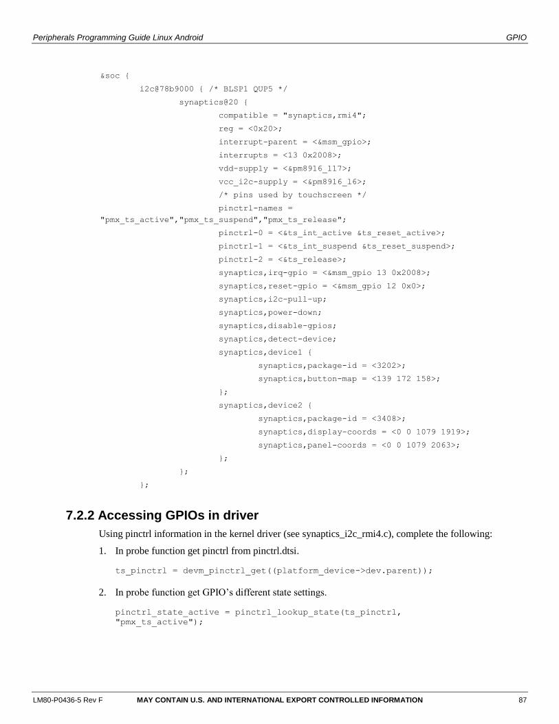
Peripherals Programming Guide Linux Android GPIO
LM80-P0436-5 Rev F MAY CONTAIN U.S. AND INTERNATIONAL EXPORT CONTROLLED INFORMATION 87
7.2.2 Accessing GPIOs in driver
Using pinctrl information in the kernel driver (see synaptics_i2c_rmi4.c), complete the following:
1. In probe function get pinctrl from pinctrl.dtsi.
ts_pinctrl = devm_pinctrl_get((platform_device->dev.parent));
2. In probe function get GPIO’s different state settings.
pinctrl_state_active = pinctrl_lookup_state(ts_pinctrl,
"pmx_ts_active");
&soc {
i2c@78b9000 { /* BLSP1 QUP5 */
synaptics@20 {
compatible = "synaptics,rmi4";
reg = <0x20>;
interrupt-parent = <&msm_gpio>;
interrupts = <13 0x2008>;
vdd-supply = <&pm8916_l17>;
vcc_i2c-supply = <&pm8916_l6>;
/* pins used by touchscreen */
pinctrl-names =
"pmx_ts_active","pmx_ts_suspend","pmx_ts_release";
pinctrl-0 = <&ts_int_active &ts_reset_active>;
pinctrl-1 = <&ts_int_suspend &ts_reset_suspend>;
pinctrl-2 = <&ts_release>;
synaptics,irq-gpio = <&msm_gpio 13 0x2008>;
synaptics,reset-gpio = <&msm_gpio 12 0x0>;
synaptics,i2c-pull-up;
synaptics,power-down;
synaptics,disable-gpios;
synaptics,detect-device;
synaptics,device1 {
synaptics,package-id = <3202>;
synaptics,button-map = <139 172 158>;
};
synaptics,device2 {
synaptics,package-id = <3408>;
synaptics,display-coords = <0 0 1079 1919>;
synaptics,panel-coords = <0 0 1079 2063>;
};
};
};
Peripherals Programming Guide Linux Android GPIO
LM80-P0436-5 Rev F MAY CONTAIN U.S. AND INTERNATIONAL EXPORT CONTROLLED INFORMATION 88
pinctrl_state_suspend = pinctrl_lookup_state(ts_pinctrl,
"pmx_ts_suspend");
3. Request the GPIO.
gpio_request(platform_data->irq_gpio, "rmi4_irq_gpio");
4. Set the GPIO direction.
gpio_direction_output(platform_data->reset_gpio, 1);
gpio_direction_input(platform_data->irq_gpio);
5. If it is an interrupt pin, request the IRQ.
int irqn = gpio_to_irq(platform_data->irq_gpio);
6. If it is a wakeable interrupt then configure as such:
enable_irq_wake(irqn);
7. Set different GPIO states when needed.
pinctrl_select_state(ts_pinctrl, pinctrl_state_active);
pinctrl_select_state(ts_pinctrl, pinctrl_state_suspend);
8. Write a value (high/low) to output the GPIO.
gpio_set_value(platform_data->reset_gpio, 1);
gpio_set_value(platform_data->reset_gpio, 0);
9. Read the GPIO status.
int value = gpio_get_value(platform_data->irq_gpio);
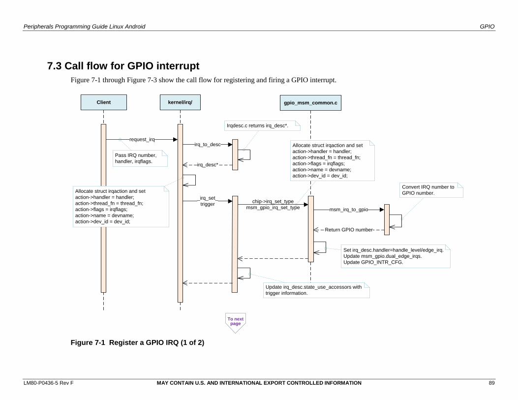
Peripherals Programming Guide Linux Android GPIO
LM80-P0436-5 Rev F MAY CONTAIN U.S. AND INTERNATIONAL EXPORT CONTROLLED INFORMATION 89
7.3 Call flow for GPIO interrupt
Figure 7-1 through Figure 7-3 show the call flow for registering and firing a GPIO interrupt.
gpio_msm_common.ckernel/irq/Client
request_irq
Return GPIO number
Pass IRQ number,
handler, irqflags.
Irqdesc.c returns irq_desc*.
Allocate struct irqaction and set
action->handler = handler;
action->thread_fn = thread_fn;
action->flags = irqflags;
action->name = devname;
action->dev_id = dev_id;
Convert IRQ number to
GPIO number.
Set irq_desc.handler=handle_level/edge_irq.
Update msm_gpio.dual_edge_irqs.
Update GPIO_INTR_CFG.
irq_desc*
_irq_set_
trigger
irq_to_desc
chip->irq_set_type
msm_gpio_irq_set_type msm_irq_to_gpio
Allocate struct irqaction and set
action->handler = handler;
action->thread_fn = thread_fn;
action->flags = irqflags;
action->name = devname;
action->dev_id = dev_id;
Update irq_desc.state_use_accessors with
trigger information.
To next page
Figure 7-1 Register a GPIO IRQ (1 of 2)
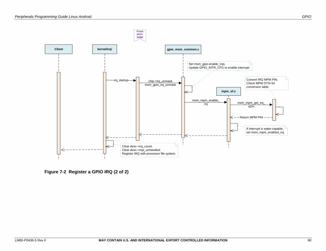
Peripherals Programming Guide Linux Android GPIO
LM80-P0436-5 Rev F MAY CONTAIN U.S. AND INTERNATIONAL EXPORT CONTROLLED INFORMATION 90
mpm_of.c
gpio_msm_common.ckernel/irq/Client
irq_startup chip->irq_unmask
msm_gpio_irq_unmask
Set msm_gpio.enable_irqs.
Update GPIO_INTR_CFG to enable interrupt.
msm_mpm_enable_
irq msm_mpm_get_irq_
a2m
Convert IRQ MPM PIN.
Check MPM DTSI for
conversion table.
Return MPM PIN
If interrupt is wake-capable,
set msm_mpm_enabled_irq.
Clear desc->irq_count.
Clear desc->irqs_unhandled.
Register IRQ with processor file system.
From prev. page
Figure 7-2 Register a GPIO IRQ (2 of 2)
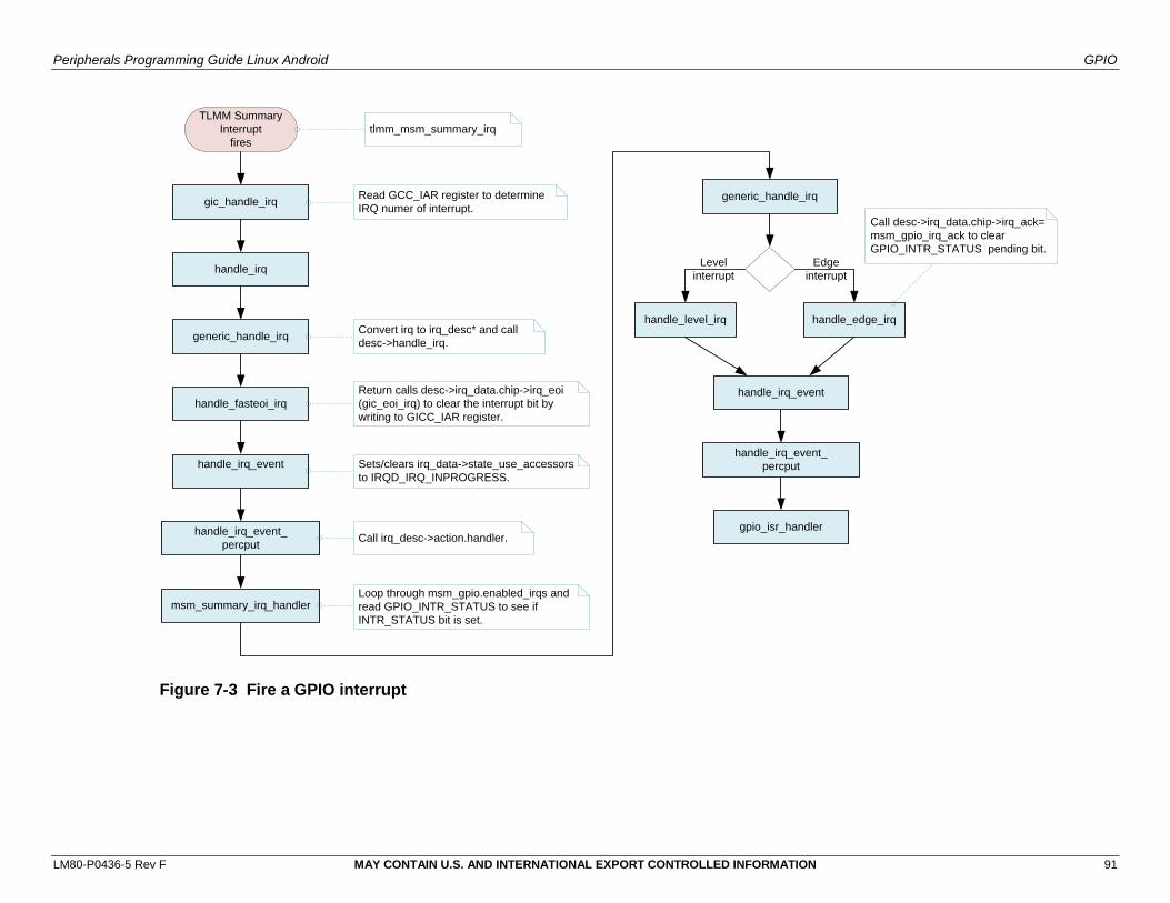
Peripherals Programming Guide Linux Android GPIO
LM80-P0436-5 Rev F MAY CONTAIN U.S. AND INTERNATIONAL EXPORT CONTROLLED INFORMATION 91
gic_handle_irq
TLMM Summary
Interrupt
fires
handle_irq
generic_handle_irq
handle_fasteoi_irq
handle_irq_event
handle_irq_event_
percput
msm_summary_irq_handler
tlmm_msm_summary_irq
Read GCC_IAR register to determine
IRQ numer of interrupt.
Convert irq to irq_desc* and call
desc->handle_irq.
Return calls desc->irq_data.chip->irq_eoi
(gic_eoi_irq) to clear the interrupt bit by
writing to GICC_IAR register.
Sets/clears irq_data->state_use_accessors
to IRQD_IRQ_INPROGRESS.
Call irq_desc->action.handler.
Loop through msm_gpio.enabled_irqs and
read GPIO_INTR_STATUS to see if
INTR_STATUS bit is set.
generic_handle_irq
handle_edge_irqhandle_level_irq
handle_irq_event
handle_irq_event_
percput
gpio_isr_handler
Call desc->irq_data.chip->irq_ack=
msm_gpio_irq_ack to clear
GPIO_INTR_STATUS pending bit.
Edge
interrupt
Level
interrupt
Figure 7-3 Fire a GPIO interrupt
Peripherals Programming Guide Linux Android GPIO
LM80-P0436-5 Rev F MAY CONTAIN U.S. AND INTERNATIONAL EXPORT CONTROLLED INFORMATION 92
EXHIBIT 1 PLEASE READ THIS LICENSE AGREEMENT (“AGREEMENT”) CAREFULLY. THIS AGREEMENT IS A BINDING LEGAL AGREEMENT ENTERED INTO BY AND BETWEEN YOU (OR IF YOU ARE ENTERING INTO THIS AGREEMENT ON BEHALF OF AN ENTITY, THEN THE ENTITY THAT YOU REPRESENT) AND QUALCOMM TECHNOLOGIES, INC. (“QTI” “WE” “OUR” OR “US”). THIS IS THE AGREEMENT THAT APPLIES TO YOUR USE OF THE DESIGNATED AND/OR ATTACHED DOCUMENTATION AND ANY UPDATES OR IMPROVEMENTS THEREOF (COLLECTIVELY, “MATERIALS”). BY USING OR COMPLETING THE INSTALLATION OF THE MATERIALS, YOU ARE ACCEPTING THIS AGREEMENT AND YOU AGREE TO BE BOUND BY ITS TERMS AND CONDITIONS. IF YOU DO NOT AGREE TO THESE TERMS, QTI IS UNWILLING TO AND DOES NOT LICENSE THE MATERIALS TO YOU. IF YOU DO NOT AGREE TO THESE TERMS YOU MUST DISCONTINUE AND YOU MAY NOT USE THE MATERIALS OR RETAIN ANY COPIES OF THE MATERIALS. ANY USE OR POSSESSION OF THE MATERIALS BY YOU IS SUBJECT TO THE TERMS AND CONDITIONS SET FORTH IN THIS AGREEMENT.
1.1 License. Subject to the terms and conditions of this Agreement, including, without limitation, the restrictions, conditions, limitations and exclusions set forth in this Agreement, Qualcomm Technologies, Inc. (“QTI”) hereby grants to you a nonexclusive, limited license under QTI’s copyrights to use the attached Materials; and to reproduce and redistribute a reasonable number of copies of the Materials. You may not use Qualcomm Technologies or its affiliates or subsidiaries name, logo or trademarks; and copyright, trademark, patent and any other notices that appear on the Materials may not be removed or obscured. QTI shall be free to use suggestions, feedback or other information received from You, without obligation of any kind to You. QTI may immediately terminate this Agreement upon your breach. Upon termination of this Agreement, Sections 1.2-4 shall survive.
1.2 Indemnification. You agree to indemnify and hold harmless QTI and its officers, directors, employees and successors and assigns against any and all third party claims, demands, causes of action, losses, liabilities, damages, costs and expenses, incurred by QTI (including but not limited to costs of defense, investigation and reasonable attorney’s fees) arising out of, resulting from or related to: (i) any breach of this Agreement by You; and (ii) your acts, omissions, products and services. If requested by QTI, You agree to defend QTI in connection with any third party claims, demands, or causes of action resulting from, arising out of or in connection with any of the foregoing.
1.3 Ownership. QTI (or its licensors) shall retain title and all ownership rights in and to the Materials and all copies thereof, and nothing herein shall be deemed to grant any right to You under any of QTI's or its affiliates’ patents. You shall not subject the Materials to any third party license terms (e.g., open source license terms). You shall not use the Materials for the purpose of identifying or providing evidence to support any potential patent infringement claim against QTI, its affiliates, or any of QTI’s or QTI’s affiliates’ suppliers and/or direct or indirect customers. QTI hereby reserves all rights not expressly granted herein.
1.4 WARRANTY DISCLAIMER. YOU EXPRESSLY ACKNOWLEDGE AND AGREE THAT THE USE OF THE MATERIALS IS AT YOUR SOLE RISK. THE MATERIALS AND TECHNICAL SUPPORT, IF ANY, ARE PROVIDED "AS IS" AND WITHOUT WARRANTY OF ANY KIND, WHETHER EXPRESS OR IMPLIED. QTI ITS LICENSORS AND AFFILIATES MAKE NO WARRANTIES, EXPRESS OR IMPLIED, WITH RESPECT TO THE MATERIALS OR ANY OTHER INFORMATION OR DOCUMENTATION PROVIDED UNDER THIS AGREEMENT, INCLUDING BUT NOT LIMITED TO ANY WARRANTY OF MERCHANTABILITY OR FITNESS FOR A PARTICULAR PURPOSE OR AGAINST INFRINGEMENT, OR ANY EXPRESS OR IMPLIED WARRANTY ARISING OUT OF TRADE USAGE OR OUT OF A COURSE OF DEALING OR COURSE OF PERFORMANCE. NOTHING CONTAINED IN THIS AGREEMENT SHALL BE CONSTRUED AS (I) A WARRANTY OR REPRESENTATION BY QTI, ITS LICENSORS OR AFFILIATES AS TO THE VALIDITY OR SCOPE OF ANY PATENT, COPYRIGHT OR OTHER INTELLECTUAL PROPERTY RIGHT OR (II) A WARRANTY OR REPRESENTATION BY QTI THAT ANY MANUFACTURE OR USE WILL BE FREE FROM INFRINGEMENT OF PATENTS, COPYRIGHTS OR OTHER INTELLECTUAL PROPERTY RIGHTS OF OTHERS, AND IT SHALL BE THE SOLE RESPONSIBILITY OF YOU TO MAKE SUCH DETERMINATION AS IS NECESSARY WITH RESPECT TO THE ACQUISITION OF LICENSES UNDER PATENTS AND OTHER INTELLECTUAL PROPERTY OF THIRD PARTIES.
1.5 LIMITATION OF LIABILITY. IN NO EVENT SHALL QTI, QTI’S AFFILIATES OR ITS LICENSORS BE LIABLE TO YOU FOR ANY INCIDENTAL, CONSEQUENTIAL OR SPECIAL DAMAGES, INCLUDING BUT NOT LIMITED TO ANY LOST PROFITS, LOST SAVINGS, OR OTHER INCIDENTAL DAMAGES, ARISING OUT OF THE USE OR INABILITY TO USE, OR THE DELIVERY OR FAILURE TO DELIVER, ANY OF THE MATERIALS, OR ANY BREACH OF ANY OBLIGATION UNDER THIS AGREEMENT, EVEN IF QTI HAS BEEN ADVISED OF THE POSSIBILITY OF SUCH DAMAGES. THE FOREGOING LIMITATION OF LIABILITY SHALL REMAIN IN FULL FORCE AND EFFECT REGARDLESS OF WHETHER YOUR REMEDIES HEREUNDER ARE DETERMINED TO HAVE FAILED OF THEIR ESSENTIAL PURPOSE. THE ENTIRE LIABILITY OF QTI, QTI’s AFFILIATES AND ITS LICENSORS, AND THE SOLE AND EXCLUSIVE REMEDY OF YOU, FOR ANY CLAIM OR CAUSE OF ACTION ARISING HEREUNDER (WHETHER IN CONTRACT, TORT, OR OTHERWISE) SHALL NOT EXCEED US$10.
2. COMPLIANCE WITH LAWS; APPLICABLE LAW. You agree to comply with all applicable local, international and national laws and regulations and with U.S. Export Administration Regulations, as they apply to the subject matter of this Agreement. This Agreement is governed by the laws of the State of California, excluding California’s choice of law rules.
3. CONTRACTING PARTIES. If the Materials are downloaded on any computer owned by a corporation or other legal entity, then this Agreement is formed by and between QTI and such entity. The individual accepting the terms of this Agreement represents and warrants to QTI that they have the authority to bind such entity to the terms and conditions of this Agreement.
4. MISCELLANEOUS PROVISIONS. This Agreement, together with all exhibits attached hereto, which are incorporated herein by this reference, constitutes the entire agreement between QTI and You and supersedes all prior negotiations, representations and agreements between the parties with respect to the subject matter hereof. No addition or modification of this Agreement shall be effective unless made in writing and signed by the respective representatives of QTI and You. The restrictions, limitations, exclusions and conditions set forth in this Agreement shall apply even if QTI or any of its affiliates becomes aware of or fails to act in a manner to address any violation or failure to comply therewith. You hereby acknowledge and agree that the restrictions, limitations, conditions and exclusions imposed in this Agreement on the rights granted in this Agreement are not a derogation of the benefits of such rights. You further acknowledges that, in the absence of such restrictions, limitations, conditions and exclusions, QTI would not have entered into this Agreement with You. Each party shall be responsible for and shall bear its own expenses in connection with this Agreement. If any of the provisions of this Agreement are determined to be invalid, illegal, or otherwise unenforceable, the remaining provisions shall remain in full force and effect. This Agreement is entered into solely in the English language, and if for any reason any other language version is prepared by any party, it shall be solely for convenience and the English version shall govern and control all aspects. If You are located in the province of Quebec, Canada, the following applies: The Parties hereby confirm they have requested this Agreement and all related documents be prepared in English.