Embed Size (px)
Citation preview

DEGREE PROGRAMME IN ELECTRICAL ENGINEERING
MASTER’S THESIS
PERFORMANCE ANALYSIS OF SYSTEM-
LEVEL BUS IN A MODEM SYSTEM-ON-CHIP
Author Tapio Hautala
Supervisor Jukka Lahti
Second Examiner Timo Rahkonen
Technical Advisor Pekka Kotila
December 2016
Hautala T. (2016) Performance Analysis of System-Level Bus in a Modem Sys-
tem-On-Chip. University of Oulu, Degree Programme in Electrical Engineering.
Master’s Thesis, 62 p.
ABSTRACT
This thesis presents a performance analysis of a system-level bus structure in a
modem system-on-chip. The high-level operations of a modem are presented and
the communication requirements inside a modem studied. The ARM AMBA 3
AHB-Lite bus protocol and the ARM multi-layer AHB interconnect used in the
modem are presented and the common arbitration schemes compared. System-
level bus latency sources, such as arbitration, memory access times and synchro-
nization, are discussed. Study into the implementation of bus performance anal-
ysis is presented, including introduction to bus traffic generation, traffic model-
ing and monitoring.
The practical part of the thesis presents the implementation of the SystemVer-
ilog-based register transfer level simulation environment created for bus perfor-
mance analysis. The environment includes the test bench and the class based ver-
ification components. The performance analysis environment is able to replace
the relevant bus masters in the modem design and model realistic bus traffic.
Simulations that mimic the downlink and uplink bus traffic were done and the
results are presented. The results show that the extreme parallelism of the bus
structure works mostly as expected. Most design masters are able to maintain
high throughput and low latencies in all tests. In the worst-case scenario, how-
ever, one bus master experiences an 81 % decrease in the average throughput due
to bus congestion. By configuring some quiet times to the masters, the results
show much lower impact. Processor’s access times to the peripherals were also
measured with the simulation environment. At least one peripheral showed too
slow access times. An optimization was made, and verified successful with the
simulation environment. The results shown in this thesis can be used in further
optimization of the bus structure. The created simulation environment can also
be used to verify the performance of future design revisions.
Key words: digital baseband, on-chip bus, arbiter, AMBA, verification IP

Hautala T. (2016) Modeemipiirin järjestelmäväylän suorituskykyanalyysi. Oulun
yliopisto, sähkötekniikan koulutusohjelma. Diplomityö, 62 s.
TIIVISTELMÄ
Tässä työssä esitetään digitaalisen modeemipiirin järjestelmäväylän suoritusky-
kyanalyysi. Työssä käsitellään modeemin korkean tason toiminnallisuutta ja
pohditaan modeemipiirin sisäisiä tiedonsiirtovaatimuksia. Modeemipiirin käyt-
tämät ARM AMBA 3 AHB-Lite -väyläarkkitehtuuri ja ARM multi-layer AHB -
väyläliitäntä kuvataan ja sovittelumenetelmiä vertaillaan. Järjestelmäväylän la-
tenssin lähteitä, kuten isäntien välistä sovittelua, muistien nopeutta ja synkro-
nointia pohditaan. Väylän suorituskykyanalyysin vaiheet, kuten väyläliikenteen
tuottaminen, mallintaminen ja tarkkailu esitetään.
Työn käytännön osuudessa esitellään suorituskykymittauksia varten kehitetty
rekisterisiirtotason simulointiympäristö. Simulointiympäristö koostuu testipen-
kistä ja luokkapohjaisista verifiointikomponenteista. Simulointiympäristö kyke-
nee korvaamaan modeemipiirin alkuperäiset väyläisännät ja mallintamaan pii-
rin väyläliikennettä vastaanotto- ja lähetystilanteissa. Tulokset osoittavat, että
väylärakenteen äärimmäinen rinnakkaisuus toimii suurimmalta osin odotetusti.
Suurin osa väyläisännistä kykenee ylläpitämään korkeaa tiedonsiirtonopeutta ja
kokee pieniä tiedonsiirtoviiveitä kaikissa testeissä. Pahimmillaan yksi väyläisäntä
kokee 81 % laskun keskimääräisessä tiedonsiirtonopeudessa väylän ruuhkautu-
misen takia. Kun simuloinneissa mallinnetaan isäntien ajoittaisia hiljaisia hetkiä,
ruuhkautumisen vaikutukset ovat huomattavasti vähäisemmät. Simulointiympä-
ristöllä mitattiin myös prosessorin tiedonsiirtoviiveitä oheislaitteisiin. Tiedon-
siirto ainakin yhteen oheislaitteeseen osoittautui liian hitaaksi. Optimointi tehtiin
ja verifioitiin onnistuneeksi simulointiympäristöllä. Työssä esitettyjä tuloksia voi-
daan käyttää väylärakenteen jatkokehittämisessä. Kehitettyä simulointiympäris-
töä voidaan myös käyttää tulevien piiriversioiden suorituskyvyn verifioimiseen.
Avainsanat: kantataajuusmodeemi, järjestelmäväylä, sovittelija, AMBA, verifi-
ointikomponentti

TABLE OF CONTENTS
ABSTRACT
TIIVISTELMÄ
TABLE OF CONTENTS
FOREWORD
LIST OF ABBREVIATIONS AND SYMBOLS
1. INTRODUCTION .............................................................................................. 9
2. MODEM OVERVIEW ..................................................................................... 11
2.1. Introduction to the modem ...................................................................... 11
2.2. Communication requirements ................................................................. 12
2.2.1. Latency ........................................................................................ 13
2.2.2. Throughput .................................................................................. 13
3. SYSTEM-LEVEL BUS .................................................................................... 15
3.1. Parallel bus .............................................................................................. 15
3.2. ARM AMBA 3 AHB-Lite ....................................................................... 15
3.3. ARM multi-layer AHB ............................................................................ 17
3.4. Arbitration schemes ................................................................................. 18
3.4.1. Static priority ............................................................................... 19
3.4.2. Round-robin ................................................................................. 19
3.4.3. Time division multiple access (TDMA) ...................................... 19
3.4.4. Other arbitration schemes ............................................................ 20
4. SYSTEM-LEVEL BUS PERFORMANCE ..................................................... 21
4.1. Latency and bandwidth ............................................................................ 21
4.2. Latency sources ....................................................................................... 21
4.2.1. Bus protocol latency .................................................................... 21
4.2.2. Arbitration latency ....................................................................... 22
4.2.3. Slave processing time .................................................................. 24
4.2.4. Clock domain synchronization .................................................... 25
4.2.5. Bus bridges .................................................................................. 27
4.3. Total latency ............................................................................................ 28
5. BUS PERFORMANCE ANALYSIS METHODS ........................................... 30
5.1. Requirements of the verification environment ........................................ 30
5.2. Stages of performance analysis ............................................................... 30
5.2.1. Traffic generation ........................................................................ 30
5.2.2. Traffic monitoring ....................................................................... 32
5.2.3. Data processing and reporting ..................................................... 33
5.3. Commercial EDA tools and verification IPs ........................................... 34
6. IMPLEMENTATION OF THE PERFORMANCE ANALYSIS..................... 36
6.1. AHB-Lite verification IPs ....................................................................... 36
6.1.1. AHB-Lite Monitor ....................................................................... 36
6.1.2. AHB-Lite Agent .......................................................................... 38
6.1.3. Validating the verification IPs ..................................................... 39

6.2. Test bench ................................................................................................ 40
6.3. Traffic pattern generation ........................................................................ 41
7. PERFORMANCE ANALYSIS RESULTS ...................................................... 44
7.1. Latency .................................................................................................... 44
7.2. Throughput .............................................................................................. 46
7.3. Intermittent traffic ................................................................................... 49
7.4. Uplink test results .................................................................................... 50
8. DISCUSSION ................................................................................................... 53
9. SUMMARY ...................................................................................................... 56
10. REFERENCES ................................................................................................. 58

FOREWORD
The purpose of this thesis was to analyze the performance of a system-level bus in a
modem system-on-chip. The thesis work was conducted at Nordic Semiconductor Fin-
land during the second half of 2016.
I would like to thank my technical advisor and boss Pekka Kotila for the amazing
opportunity to work at Nordic. Thank you also to my colleagues who have always been
willing to help me. Thanks for sharing just a tiny bit of your vast knowledge in modem
design. Special thanks to Senior R&D Engineer Hannu Talvitie for his guidance during
the practical part of the thesis. Thank you also to professor Timo Rahkonen for review-
ing my thesis. Lastly, a big thank you to Chief Engineer Jukka Lahti for acting as my
thesis supervisor. More importantly, I would like to thank him for the amazing work
he does every day at the university.
Oulu, December 20, 2016
Tapio Hautala
LIST OF ABBREVIATIONS AND SYMBOLS
AHB Advanced High-performance Bus
AMBA Advanced Microcontroller Bus Architecture
APB Advanced Peripheral Bus
ARM Advanced RISC Machines
BE Best-effort
BFM Bus Functional Model
DMA Direct Memory Access
DP Dynamic Priority
DRAM Dynamic Random Access Memory
DSP Digital Signal Processor
DUT Design Under Test
EDA Electronics Design Automation
EEPROM Erasable Programmable Read-only Memory
FIFO First-In-First-Out
FPGA Field Programmable Gate Array
GT Guaranteed throughput
GUI Graphical User Interface
HDL Hardware Description Language
IP Intellectual Property
ISR Interrupt Service Routine
IS Ideal-slave
ISS Instruction Set Simulator
MAC Media Access Control
NOC Network-On-Chip
PHY Physical layer
QAM Quadrature Amplitude Modulation
TDMA Time Division Multiple Access
RF Radio Frequency
ROM Read-only Memory
RTL Register Transfer Level
SVI SystemVerilog Interface
SM Self-motivated
SoC System-on-chip
SQL Structured Query Language
SRAM Static Random Access Memory
SVI SystemVerilog Interface
UML Unified Modeling Language
UVM Universal Verification Methodology
VMM Verification Methodology Manual
WRR Weighted-Round-Robin
B burst data cycle length
buswidth data width in bits
c1 constant, depends on implementation of the bus structure
c2 constant, depends on implementation of the bus structure

CLKget receiver clock frequency
CLKput sender clock frequency
CUR channel utilization ratio
dataput bus data
fCLK bus clock speed in Hz
Nbridge bus bridge count
ND number of transfers
Nm number of masters
Nsync number of synchronizers
Ta average arbitration latency
Tamin default arbitration latency
Tbridge bridging time
Tbus bus protocol latency
Tidle time the master uses for processing the data in between bus transfers
Tslave slave access time
Tsync number of clock cycles consumed in synchronization and due to
slower slave clock speed
Ttotal total latency (time)

1. INTRODUCTION
The on-chip communication architecture provides the means of communication inside
a system-on-chip (SoC). It provides correct connections from the source components
to their destinations. In addition, the communication must be fast and predictable. The
on-chip communication architecture has a major impact on the performance and power
consumption of modern SoCs. The communication delays in the on-chip communica-
tion architecture present a major cause of bottlenecks in many SoCs. [1 p. ix, 6 and
101] The selection of the bus (type, width and topology) is one of the most complex
tasks of SoC design [2].
This thesis studies a wireless modem SoC (also known as the baseband processor
and the digital baseband). A modem is a hard real time system. The communication
processing must be done repeatedly on time and the communication standard sets the
required throughput (bit/s) for the system. [3] Individual read/write transfer times are
not usually critical. However, if a device cannot maintain the required throughput for
an extended period of time, the operation of the system can be compromised. [4] The
communication network of a real-time system should then be predictable. Guarantees
should be made for maximum latency and minimum throughput. [5]
The thesis presents the performance analysis of chip level communication in a mo-
dem. The backbone connecting all the processing elements inside the studied modem
is the system-level bus. The goal of the work is to create a register transfer level (RTL)
verification environment that is able to measure the clock accurate latencies and aver-
age throughputs of all the relevant bus masters of the modem running simultaneously.
In order to model realistically the bus congestion the simulations imitate real downlink
and uplink bus traffic. RTL simulation is chosen because it allows clock accurate,
functional modeling of the digital design [6, p. 91]. The analysis is done with no design
RTL changes to make the performance analysis environment easily reusable with fu-
ture design revisions.
The work is done in order to characterize and validate the performance of the sys-
tem-level bus structure. This leads to the possibility to optimize the bus structure. A
possible optimization would be for instance a change in the interconnects’ arbitration
scheme or master/slave bus clock speed. The verification environment creates a plat-
form for iterative performance optimizations. The probable use case is not to revamp
the whole bus structure, but rather to point out the places where small changes matter
the most. The environment can then also be used to verify that the optimizations pro-
vide the expected performance.
Chapter 2 explains the high level functions of a modem. It shows how the baseband
processing links together the whole transceiver chain. An overview to the structure of
the studied modem is shown and the SoCs internal communication requirements dis-
cussed.
Chapter 3 introduces the system-level bus connecting the intellectual property (IP)
operating inside the modem. The interconnect structure used in the modem and the
common arbitration schemes are presented.
Chapter 4 introduces the concepts of latency and bandwidth. The relation of these
concepts is shown and the latency sources slowing down the transfers presented.

10
Chapter 5 lists the requirements set for the performance analysis environment. The
performance analysis is broken down into three stages: traffic generation, traffic mon-
itoring and data processing. Previous work done in this area is studied and some com-
mercial performance analysis tools presented.
Chapter 6 presents the implementation of the performance analysis as done by the
author. The implementation contains multiple class based verification IPs and the sim-
ulation test bench. The verification IPs are used in replacing the real bus masters of
the design. Modeling of the realistic bus traffic is then discussed and the types of tests
presented.
Chapter 7 shows the simulation results from the downlink and uplink simulations.
Some performance updates were made and the before and after results are presented.
Chapter 8 reviews the thesis work. The results are discussed and the future prospects
of the verification environment and the IPs are analyzed.
Chapter 9 gives a recap of the thesis. The main contents of the thesis are summarized
and the final results presented.

11
2. MODEM OVERVIEW
Chapter 2.1 introduces the digital baseband processing and the structure of the studied
modem. Chapter 2.2 discusses the communication requirements inside a modem sys-
tem-on-chip (SoC).
2.1. Introduction to the modem
The design studied in this thesis is a wireless modem. It includes the digital processing
done at the physical layer (PHY) of a wireless transceiver. A high-level representation
of the functions in the modem is shown in Figure 1.
EncryptionChannel
codingModulation
DecryptionChannel
decodingDemodulation
MACTX data...
MACRX data... Front-end
Front-end
Transmitter (digital)Application
(digital, sofware)
Receiver (digital)
RF
(analog)
Application
(digital, sofware)
RF
(analog)
Figure 1. Digital baseband processing.
The data is passed to the transmitter from the higher layers through the media access
control (MAC). In the digital processing, the data is first encrypted. Channel coding is
then applied to improve reliability with data redundancy. The coded data is then in
modulation mapped into constellation points and sent via the front-end to the analog
processing and antenna. The front-end is a mix of analog and digital processing. The
functionalities of the front-end include filtering, upconversion from baseband to radio
frequency (RF), digital-to-analog conversion and amplification. At the receiver side,
the corresponding operations are done as shown in Figure 1. [7]
In the studied modem the digital baseband processing is done with dedicated hard-
ware accelerators and a processor. The components are connected to multiple memo-
ries via the system-level bus structure. A simplified block diagram of the modem SoC
is shown in Figure 2.

12
Dedicated
memory
Hardware
accelerator
Hardware
acceleratorProcessor
Memory MemoryPeripherals
Modem
Front-end
IO
Interconnect fabric
Interconnect
Interconnect
Interconnect
Figure 2. Simplified block diagram of the studied modem.
The distributed nature of the processing in the modem means that a lot of communica-
tion is needed between the hardware accelerators and the processor. This internal com-
munication happens using parallel buses through the interconnect fabric. The memo-
ries are used in storing and retrieving the information, and in order to pass the data to
the next processing element. The interconnect fabric consists of multiple interconnects
that allow parallel accesses from the hardware accelerators and the processor to the
memories and peripherals.
2.2. Communication requirements
Transceiver is a real-time system. The communication standards impose hard dead-
lines on processing times and specify requirements for data throughput (bit/s). [3] The
communication requirements in a real-time system can be divided into two categories:
best-effort (BE) and guaranteed throughput (GT). Best-effort traffic is characterized
by irregular throughput needs but high sensitivity for transfer times (latency). Guaran-
teed throughput traffic requires a set, minimum throughput but only a coarse worst-
case latency guarantee for the longer transfer sequences. Typical latency sensitive de-
vice is a processor executing application software that has response time requirements
such as controlling a display. Typical guaranteed throughput requestors are applica-
tions that require real-time guarantees such as communication and video processing.
[8] The following chapters discuss the communication requirements in the digital base-
band processing.

13
2.2.1. Latency
Baseband processing is a hard real time procedure, meaning that all processing must
be done on time. The communication standard sets specific time limits for certain op-
erations. For example, the symbol processing done in the front-end and in demodula-
tion must be executed within the specified symbol period. As an example, for IEEE
802.16e (Mobile Broadband Wireless Access System) the symbol period is 23.15 µs
and for DVB-H (Digital Video Broadcasting - Handheld) the symbol period is 462 µs.
[7] The individual data transfer times on the system-level bus are many orders of mag-
nitude smaller than the processing times specified in the communication standards.
Defining hard requirements on individual bus transfers is then unrealistic and depends
heavily on the implementation.
There are some situations where the individual transfer times matter. One example
is the processor interrupt latency or the number of clock cycles it takes for the proces-
sor to respond to an interrupt request. The responsiveness of a system depends heavily
on the time it takes to fetch the interrupt service routines (ISR) from memory. [9]
The second concern with long transfer times is power consumption. Modern proces-
sors typically have the ability to enter sleep state when no processing is required. The
sleep state dramatically reduces the power consumption of the processor. Depending
on the implementation, if the processor does a read or a write access to a device that
has a slow access time, the processor must stay awake and wait for the data to go
through before it can go back to sleep. The time the processor stays awake is higher
and power consumption is increased. There are devices such as the DMA (Direct
Memory Access) controllers that can alleviate this problem. DMA controllers can in-
dependently move data between two places such as from memory to memory or be-
tween memory and IO. This allows the processor to offload transfers to the DMA con-
trollers and enter sleep state, reducing power consumption. [10]
Another form of increased power consumption comes from the fact that high
memory access times increase the overall application execution times. The processor
must then stay awake for a longer time, which increases power consumption. In order
to increase performance and decrease power consumption the processor can utilize a
fast local cache memory. [11]
2.2.2. Throughput
The performance of a communication link is usually described by the user data rate in
bits per second. The data sent over the air, however, contains additional information
such as information used for synchronization and error correction [12, p.116]. For this
reason, the throughput requirements inside the modem SoC are not completely defined
by the user data rate.
In the receiver, after down conversion the signal is sampled in the digital baseband.
The required sampling rate can be calculated from the symbol interval specified in the
communication standard. The IEEE 802.11a (Wi-Fi) receiver is used as an example in
the calculations in this chapter. For 802.11a, the specified symbol interval is 4.0 µs.
The 802.11a uses 52 subcarriers in total, of which 4 are used for synchronization (pilot
subcarriers) and 48 for the data symbols. [13] The required sampling rate is then 52
samples / 4.0 µs = 13 MS/s. The number of bits per sample and therefore the actual
sampling bit rate depends on the implementation.

14
After sampling, the data is retrieved from the samples by demodulation. In 802.11a
with the fastest data rate the modulation method used is 64-QAM (Quadrature Ampli-
tude Modulation) with 6 bits of data per constellation point (log2 (64)). The data rate
after demodulation is then 13 MS/s ∙ 48/52 ∙ 6 bit/S = 72 Mb/s.
After demodulation, the data still contains the parity bits from the channel coding
done at the transmitter. The number of parity bits depends on the coding rate used.
With the fastest data rate for 802.11a, this is ¾. The data rate after channel decoding
is then 72 Mb/s ∙ ¾ = 54 Mb/s. [12, p.116] This is the data rate as specified in the IEEE
802.11a standard [13]. Figure 3 shows the throughput requirements in the digital base-
band operation of an 802.11a receiver.
Channel
decodingDemodulation
≥13 MS/s ∙ N b/S 72 Mb/s 54 Mb/s
received samples coded blocks data
Figure 3. IEEE 802.11a receiver throughput requirements.
As can be seen in Figure 3 the throughput requirements vary during the digital pro-
cessing phases of the receiver. The internal communication structure in the SoC must
be able to provide the required bandwidths for the modem to function. Similar analysis
can be done for the transmitter and with different communication protocols and con-
figurations.

15
3. SYSTEM-LEVEL BUS
This chapter concentrates on SoC level communication. Chapter 3.1 gives an intro-
duction on the parallel bus. Chapters 3.2 and 3.3 describe the bus interfaces and inter-
connects used in the studied modem. Chapter 3.4 introduces different bus arbitration
schemes used in handling converging traffic from multiple sources.
3.1. Parallel bus
The system-level communication of an SoC is typically implemented with parallel
buses. This is also the case for the studied modem. Parallel bus is a set of wires that
transmit data multiple bits at a time. Generic depiction of a parallel bus is shown in
Figure 4 [1, p. 20].
Master Data signal lines Slave
Control signal lines
Address signal lines
Figure 4. Parallel bus.
Figure 4 shows that the bus provides means of transferring data between the bus
master and slave. Address signal lines are used in directing the traffic to the correct
slave. Data signal lines carry the read and write data. Control signals bring additional
information, such as the state of the transfer. Bus master always initiates the data trans-
fer. It either writes data to the slave or requests a read from the slave. Slaves respond
to the transfer requests of masters. Typical bus masters are processors, DSPs (Digital
Signal Processors) and other DMA-capable bus devices. Typical bus slaves are on-
chip and off-chip memories and peripheral devices. [1, p. 17-19] Some examples of
widely used on-chip bus architectures are: ARM AMBA AHB and AXI, IBM Core-
Connect PLB, Sonics Smart Interconnect SonicsMX and STMicroelectronics STBus
Type 3. [1]
3.2. ARM AMBA 3 AHB-Lite
The main system-level bus interface of the studied modem is the ARM AMBA 3 AHB-
Lite (Advanced High-performance Bus). AHB-Lite is a high-performance synthesiza-
ble bus interface. It is provided for the SoC designers as HDL (Hardware Description
Language) code that can be implemented with logic synthesis tools. AHB-Lite is part
of the AMBA 3 (Advanced Microcontroller Bus Architecture) specification, which is
an open standard developed by ARM (Advanced RISC Machines) for on-chip com-

16
munications. AHB-Lite was developed in 2006 as a successor to the AHB bus inter-
face. [14] It supports wide data buses ranging from 32-bits to 1024-bits. The bus mas-
ter interface is shown in Figure 5. [15]
AHB-Lite
master
HWDATA[31:0]
HWRITE
HCLK
HADDR[31:0]HREADY
HRESP
HRESETn
HRDATA[31:0]
HSIZE[2:0]
HBURST[2:0]
HPROT[3:0]
HTRANS[1:0]
HMASTLOCK
Transfer
response
Global
signals
Data
Address
and
control
Data
Figure 5. AMBA 3 AHB-Lite master interface.
As seen in Figure 5 the master contains ready (HREADY) and error (HRESP) re-
sponse signals which come from the slave. Other input signals are clock (HCLK), ac-
tive low reset (HRESETn) and read data (HRDATA). Output signals contain the slave
address (HADDR), read/write indicator (HWRITE), byte count of the transfer
(HSIZE), sequential transfer count indicator (HBURST) and write data (HWDATA).
HTRANS indicates the transfer type, such as, idle, non-sequential (NONSEQ) and se-
quential (SEQ). HMASTLOCK signal is used to signal that the transfer sequence must
be processed without interruptions. The HPROT signal contains special additional in-
formation on the transfer. It contains for example information whether the transfer is
an opcode fetch or a data access. The slave interface is presented in Figure 6. [15]
AHB-Lite
slave
HWDATA[31:0]
HWRITE
HADDR[31:0]
HREADYOUT
HRESP
HRDATA[31:0]
HSIZE[2:0]
HBURST[2:0]
HPROT[3:0]
HTRANS[1:0]
HMASTLOCK
Data
HCLK
HRESETnGlobal
signals
HSELx
Address
and
control
Select
Transfer
response
Data
HREADY
Figure 6. AMBA 3 AHB-Lite slave interface.
The slave interface as shown is almost the mirror image of the master interface. The
select signal (HSELx) is used to indicate to the slave that the current transfer is in-
tended for it. More information on these signals can be found at the ARM AMBA 3
AHB-Lite protocol specification [15].
An AHB-Lite bus transfer consists of two phases: Address phase and Data phase.
The simplest transfer takes two clock cycles; one for addressing and one for data trans-
fer. A waveform of a simple write transfer is shown in Figure 7. [15]

17
A B
Data (A)HWDATA[31:0]
HWRITE
HCLK
HADDR[31:0]
HREADY
HRESP
Address phase Data phase
Figure 7. AHB-Lite simple write.
In this example, at the start of the Address phase the master drives the HWRITE
high to indicate a write transfer. Master also controls the HADDR which defines the
receiving slave. Slave uses the HREADY to signal that it is ready to continue the trans-
fer to the Data phase. In the Data phase the bits in the HWDATA are read by the slave
and HREADY is raised to signal the end of the transfer. Slave can also raise the
HRESP signal to indicate an unsuccessful transaction. [15]
In Figure 7 the pipelined nature of AHB-Lite can also be seen. During the Data
phase of transfer A, the Address phase of transfer B occurs. Overlapping of Address
and Data phases improves performance. [15]
3.3. ARM multi-layer AHB
Usually SoCs have the requirement for multiple masters. The modem studied has for
example such masters as processor and dedicated hardware accelerators. All of these
masters need to be able to access the memory and peripheral slaves. The AHB-Lite
bus standard supports only single-master multi-slave connections. In order to connect
multiple masters to multiple slaves the multi-layer AHB interconnection scheme was
developed by ARM. This interconnection scheme creates so called “layers” for every
master. Because every layer consists of only one master, the masters and slaves can
use the AHB-Lite bus interfaces. At the backbone of the studied modem is the ARM
multi-layer AHB bus interconnect. The simplest implementation of a multi-layer AHB
interconnect is shown in Figure 8. [16]

18
Input
stage
Decoder
Master
2
Decoder
Arbiter
Arbiter
Slave
1
data
Master
1addr. &
control
dataInput
stage
Multi-layer AHB interconnectLayer 1
Layer 2
Slave
2
addr. &
control
data
addr. &
control
addr. &
control
data
Figure 8. Multi-layer AHB interconnect.
In multi-layer AHB, two layers cannot access the same slave at the same time. This
creates a situation where masters have to “compete” for the slave resources. The arbiter
within the interconnect determines which layer has the highest priority and gets the
access to the slave. The “multiplexer” components drawn route the traffic in both di-
rections, acting as multiplexer and demultiplexer. The input stage is used to store the
address and control information of the master that has to wait for the slave access. The
master is made to wait by lowering the HREADY signal. The address decoder routes
the read and write traffic based on the layer’s HADDR address bits. The selection is
done by driving the HSEL signal of the appropriate slave high. [16]
3.4. Arbitration schemes
ARM defines in the multi-layer AHB specification that every slave port must have an
arbiter. The arbiter, as previously mentioned, makes the decision which layer is given
access to the slave. The specification leaves the implementation of the arbitration
scheme for the designer. This means that the arbiter can service the layers in multiple
ways. [16]
There are many different arbitration schemes created for different applications.
These arbitration schemes i.e., scheduling strategies can be applied not just on the bus
arbiter, but also more generally at hardware and software scheduling. The main de-
nominator is a system that manages a shared resource. In the context of hardware bus,
the shared resource is a bus memory slave. In the software context, a shared resource
can be a process or an instance of a program. [17, p. 172] In the next chapters the three
main types of arbitration schemes are presented. These are: static priority, round-robin
and time division multiple access (TDMA). [1] The chapters concentrate on the hard-
ware bus viewpoint and are applicable to ARM multi-layer AHB interconnect.

19
3.4.1. Static priority
In this arbitration scheme, the masters are given fixed priorities. If multiple masters
are trying to access the same slave at the same time the highest priority master is al-
ways given the access. This is a simple arbitration scheme and one of the most com-
monly used. It provides high performance for the high priority masters. In a crowded
bus, there is a possibility that some lower priority masters have to wait a long time for
the access or the access might never be granted. [1]
3.4.2. Round-robin
In round-robin (token passing) arbitration, the priorities change at every transfer. The
master with the highest priority (i.e. with the token) changes in circular (round-robin)
fashion. If the master with the highest priority does not need to access the slave the
token is given to the master with the next highest priority. [18] Figure 9 depicts a basic
round-robin arbiter with four masters (M1-M4) and one slave (S).
S
M1 M2 M3 M4
M3
M1
M4 M2
Round-robin arbiter
Figure 9. Round-robin arbiter.
Round-robin arbitration scheme guarantees that every master is given opportunity
for equal bandwidth. It gives fair access for every master to the slave. The maximum
wait time is predictable and proportional to the number of masters. The scheme also
ensures that the unused time slots are usable by the lower priority masters. [18]
The basic round-robin arbitration scheme can be slower than static priority scheme
for some masters. This comes from the nature of fairness where all masters are given
equal bandwidth. [1, p. 27] There exists variations of the round-robin such as the
Weighted-Round-Robin (WRR) that are meant to tackle this issue. In WRR, every
master is given “credits” or “shares” and after each transfer, one credit is deducted.
When master runs out of credits the next master is selected in round-robin fashion.
Critical masters can be given more credits, which means they get more bandwidth.
After all masters have run out of credits, they are reloaded. The drawback of the WRR
arbitration is increased complexity compared to the basic round-robin. [19]
3.4.3. Time division multiple access (TDMA)
In TDMA arbitration scheme masters are given fixed time frames for transfers. Mas-
ters that need more bandwidth can be given longer time frames. The scheme ensures

20
high bandwidth for critical masters while ensuring that lower priority masters are even-
tually served. [1, p. 27] TDMA arbitration is pictured in Figure 10 [20].
Master 1
Master 2
Master 3
timetime
frame 1
time
frame 2
time
frame 3
time
frame 4
time
frame 5
time
frame 6
Figure 10. TDMA arbitration.
The darkened areas of the time frames in Figure 10 represent the actual used transfer
times by the masters. The decision on the lengths of the time frames is crucial for
ensuring high bandwidth allocation. As an example, in Figure 10 the Master 3 uses
only under 50 % of the available time frame. This causes a lot of wasted time and
bandwidth. [1, p. 27]
The advantage of TDMA arbitration is that it guarantees fixed bandwidths for the
masters. When properly designed, it gives high performance for critical masters but
with unpredictable or changing traffic, it cannot match the bus allocation of a round-
robin arbiter. [20] That said, due to its predictability it is an attractive option in many
real-time applications. [21]
3.4.4. Other arbitration schemes
There are multiple arbitration schemes besides the more traditional ones described in
the previous chapters. For instance, the studied modem uses a programmable priority
based arbitration scheme. It allows the application to control the priorities of the mas-
ters at run time. Another form of a run-time based arbitration scheme is the dynamic
priority (DP) scheme. It can adapt the priorities of masters dynamically based on the
changing traffic profiles of the application. [1]
Some multi-level arbitration schemes also exist. One implementation uses TDMA
as the first arbitration principle and the unused timeframes are then allocated using
round-robin arbitration [20]. The self-motivated (SM) arbitration scheme changes the
priority policy during runtime between: fixed priority, round-robin and dynamic pri-
ority. It can also change the unit of arbitration between single transfer or multiple
transfers depending on the needs of the masters. The performance is increased by 19
% - 47 % but the drawback is 9 % - 25 % larger interconnect area compared to the
more traditional arbitration schemes. [22]
21
4. SYSTEM-LEVEL BUS PERFORMANCE
This chapter presents a study on the main factors that define the performance of a
system-level bus. Chapter 4.1 introduces latency and bandwidth and shows how these
concepts are related. Chapters 4.2.1-4.2.5 introduce the main causes for latency in a
system-level bus. Finally, Chapter 4.3 presents the equation for total latency.
4.1. Latency and bandwidth
Latency and bandwidth are the terms usually used in describing the performance of a
communication link, such as a system-level bus. Latency is defined as the time it takes
for a single or multiple transfers to finish. Bandwidth is the physical limit of the chan-
nel for transfer speed (bit/s). Effective bandwidth or throughput defines the actual
achieved data rate. [23, p. F13-F15]
Throughput and latency are closely related concepts. The relationship of the total
latency and the throughput is shown in Equation 1
𝑇ℎ𝑟𝑜𝑢𝑔ℎ𝑝𝑢𝑡 =𝑁𝐷
𝑇𝑡𝑜𝑡𝑎𝑙∙ 𝑓𝐶𝐿𝐾 ∙ 𝑏𝑢𝑠𝑤𝑖𝑑𝑡ℎ, (1)
where Ttotal is the total latency (time) in clock cycles, ND is the number of transfers,
buswidth is the data width in bits and fCLK is the bus clock speed in Hz [24]. From
Equation 1 it can be seen that the throughput of a bus can be increased by making the
data bus wider, increasing the bus clock speed or reducing the total latency. Wider bus
means increased area, and higher clock speed increases power consumption [25]. The
total latency depends on the bus utilization and transmission time (or latency) of the
individual transfers [26].
4.2. Latency sources
The following chapters present a study on the typical sources of latency in a system-
level bus. Ways of lowering the transaction latencies are also discussed in the chapters.
4.2.1. Bus protocol latency
As previously discussed in Chapter 3.2 the simple AHB-Lite data transfer takes two
clock cycles: one for addressing and one for the data phase. This is defined as a transfer
latency of two clock cycles. Latency can also be defined with regards to time. With for
example 100 MHz clock speed the two clock cycle latency would equal to 20 ns.
AHB-Lite bus protocol supports pipelining. This means that if a single or multiple
masters do consecutive transactions the address and data phases overlap. This was il-
lustrated previously in Figure 7 in Chapter 3.2. The same pipelining effect happens
also if a master does a burst transaction. A four-beat incrementing burst read is shown
in Figure 11. [15]

22
NONSEQ
HBURST[2:0]
HWRITE
HCLK
HTRANS[1:0]
HRDATA[31:0]
SEQ SEQ SEQ
0x38HADDR[31:0] 0x3C 0x40 0x44
HSIZE[2:0]
INCR4
Word
HREADY
*0x3C *0x40 *0x44*0x38
Figure 11. Four-beat incrementing burst read.
In an incrementing burst as shown in Figure 11 the address is incremented between
every transfer. The Figure 11 shows that only the first transfer (address 0x38) takes
two clock cycles and due to pipelining, the next transfers finish in the following three
clock cycles. This shows that with a long burst the average latency per transfer ap-
proaches one clock cycle.
Cho Y-S. et al. defined an equation describing the total latency of single master
doing multiple transfers in a shared AMBA 2 AHB bus [27]. Because AHB-Lite re-
moves the request and grant signals of the AMBA 2 AHB, thus, reducing the single
transfer latency by one clock cycle, the equation for the total transaction latency Tbus
can be rewritten as follows for the AHB-Lite bus
𝑇𝑏𝑢𝑠 = 2 ∙ 𝑁𝐷 ∙ 𝑆 + [𝑁𝐷 ∙ (1 − 𝑆)
𝐵+ 𝑁𝐷 ∙ (1 − 𝑆)] , (2)
where ND is the data cycle count, S(0≤S≤1) is the proportion of single transfers and B
is the burst data cycle length. Equation 2 can be used in calculating the number of
clock cycles it takes to do ND number of transfers in a bus containing one master and
one or multiple slaves. This can be one layer in a multi-layer AHB interconnect. Equa-
tion 2 shows that by using the burst transfers the total transaction latency can be re-
duced [27]. It should be noted that burst transfers do not offer performance improve-
ments over back-to-back NONSEQ transfers in AHB-Lite because the pipelining ef-
fect also applies to those as discussed previously. This means that the B in Equation 2
can just as well denote the count of continuous NONSEQ transfers.
4.2.2. Arbitration latency
As discussed previously in Chapter 3.4 the arbitration resolves conflicts caused by
simultaneous accesses to a shared resource. Consequently, when one master is given

23
access to the slave others must wait. This wait time is called arbitration latency [26].
Figure 12 demonstrates a situation where two masters A and B are trying to write data
to the same slave at the same time.
NONSEQ
HWDATAA[31:0]
HCLK
HTRANSA[1:0]
HREADYA
Data (A)
NONSEQ
HWDATAB[31:0]
HTRANSB[1:0]
HREADYB
Data (B)
slave
B
A
slave
B
A
Arbitration
latency
Figure 12. Simultaneous write by two masters to the same slave.
In Figure 12 the master A is given higher priority and the first access to the slave.
This causes the data phase of master B to be extended by one clock cycle. This demon-
strates that even though the simple AHB-Lite transfer takes two clock cycles the trans-
fer time can be extended by the traffic generated by the other masters accessing the
slave. Arbitration creates a situation where transfer latencies of masters depend on the
other masters and the congestion of the slave. The average arbitration latency Ta of a
shared bus can be estimated with the following equation
𝑇𝑎 = 𝑐1 ∙ (𝑁𝑚 − 1) ∙ 𝑒𝑐2∙𝐶𝑈𝑅 + 𝑇𝑎𝑚𝑖𝑛, (3)
where c1 and c2 are constants, Nm is the number of masters, CUR is the channel
utilization ratio and Tamin is the default arbitration latency. CUR represents the number
of clock cycles the channel between masters and the slave is active, divided by the
total cycle count. [26] Default arbitration latency Tamin depends on the implementation
of the arbitration logic. More complex schemes can consume more than one clock
cycle in the arbitration process. Since arbitration happens for every transaction, a
multi-cycle arbiter can severely reduce the bus performance. This shows the drawback
of complex arbitration schemes. [1, p. 27]

24
Equation 3 shows that the latencies of transfers can vary in time based on the current
traffic conditions at the interconnect [26]. In order to ensure predictable maximum
latencies for all masters, a fair arbitration scheme, such as round-robin or TDMA,
should be used [18] and [1, p. 27].
One way of lowering the arbitration latency for a master is using the burst transfers
and burst transaction based arbitration. This way the master gets an exclusive access
to the slave for the whole duration of the burst. Burst transfers can, however, have
negative impact on the performance of other masters. The reason for this is that the
master doing the burst transactions can reserve the slave for a long time. [28] An AHB-
Lite feature called “early burst termination” can be used to enable the use of long bursts
and at the same time remove the possibility of master latency constraint violations.
The feature allows the interconnect arbiter to terminate a burst transaction if there are
pending bus transfers from other masters and the burst is taking too long to finish. [15
and 11]
Choosing the arbitration scheme that gives the best overall performance is not a
straightforward task. Minimizing the latencies might not always be the best strategy
because low arbitration latencies for some masters usually mean high latencies for
others. If the real-time application needs impose timing constraints, the arbitration
must be designed in a way that these constraints are met. The optimal bus arbitration
scheme is heavily application specific. The performance of the arbitration depends on
the type of traffic (single, burst) and the amount of traffic (a lot of internal versus a lot
of bus traffic). [22]
4.2.3. Slave processing time
In the previous examples, the slave is able to process the transaction without additional
delays. So called ideal-slave (IS) latency model as proposed by Cho Y-S. et al. and
rewritten version presented in Equation 2 in Chapter 4.2.1 disregards the processing
times of the slaves. It expects the slave to require no wait-states in the bus. [27] This
is not true for every slave device such as certain memories. Figure 13 demonstrates
how the slave can delay the transfer by inserting wait states.
A B
Data (A)HWDATA[31:0]
HWRITE
HCLK
HADDR[31:0]
HREADY
Address phase Data phase
Figure 13. Read transfer with two wait states.
Figure 13 shows the slave adding two wait states to allow extra time for it to process
the read request. [15] Wait states extend the data phase of the transfer and are seen as
additional latency by the master. Slow slaves can also lower the overall bus perfor-
mance because every wait state might delay multiple masters waiting to get access to
the slave.

25
Different memories represent the typical slow slave components. There are two
types of memories used in embedded systems: volatile and non-volatile. Volatile
memory loses its contents when the power goes down. Non-volatile memory retains
the data at power off. Typical on-chip volatile memories, such as SRAM (Static Ran-
dom Access Memory) and embedded DRAM (dynamic RAM) are used for storing the
application data. On-chip non-volatile memories, such as ROM (Read-only Memory),
EEPROM (Erasable Programmable Read-only Memory) and Flash EEPROM, are
used for storing the firmware images, operating configurations and other data. [29]
The performance of different memories varies greatly. SRAM is essentially a big
array of latches and guarantees single-cycle access times [30]. Embedded DRAM
gives comparable performance to SRAM in smaller size but with added manufacturing
complexity [29]. Modern EEPROM access times are in the range of 20-40 nanosec-
onds [31]. With for example 100 MHz clock speed this would be 2 to 4 clock cycles.
Flash is a simpler structure than EEPROM but loses the ability for single cell erase
[29]. Typical NOR Flash random access times are between 30 and 90 ns [32, p. 126]
With 100 MHz clock speed this equates to 3 to 9 clock cycles.
4.2.4. Clock domain synchronization
It is getting increasingly difficult to distribute a globally synchronous clock signal for
the whole SoC. The system-level bus spans a large area of the chip and thus operates
on multiple clock domains. The data communication between different clock domains
must be synchronized. This is to avoid erroneous register states due to metastability.
Metastability can happen when signal changes value near the rising clock edge, inside
the setup or hold time of the register. However, the synchronizer components have the
drawback of increased transfer latencies. [25]
Synchronizer IPs are provided by the bus IP vendors or they can be designed spe-
cifically for the application. ARM for example provides asynchronous and synchro-
nous AHB-AHB bridges (synchronizers) in their AMBA Design Kit. ARM asynchro-
nous AHB-AHB bus bridge is shown in Figure 14 [33]
Asynchronous
slave
AHB signals
Control
signals
AHB
M
Asynchronous
master
Synchronizer
registers
HCLKMHCLKS
AHB
S
Ahb2AhbAsync
Figure 14. ARM asynchronous AHB-AHB bridge.
This bridge component is not intended for performance applications, as stated by
ARM, due to increased overhead caused by the synchronizer registers [33]. One per-
formance-oriented approach is the AMBA wrapper designed by Kim N-J et al. [25].
This approach, however, requires the clock domains to be synchronous. The wrapper
works by latching the AHB control signals and minimizes additional delays. The third
approach to bus synchronization is the usage of mixed-clock FIFOs (First-In-First-

26
Out). The FIFO can be used to pass data between different asynchronous or synchro-
nous clock domains. An implementation of mixed-clock FIFO is shown in Figure 15.
[34]
CellCell Cell Cell
Put
Controller
Full Detector
reqput
dataput
CLKput
full
Get
Co
ntr
oll
er
Empty Detector
reqget
dataget
CLKget
empty
enput
engetvalidget
Figure 15. Mixed-clock FIFO.
The put (sender) interface is controlled by the CLKput clock. Bus data is transferred
to the cells in sequential fashion via the dataput line. The receiver reads data sequen-
tially via the get interface controlled by the CLKget clock. In this implementation, only
the global control signals full and empty need to be synchronized. With the synchro-
nization, the dataget does not go metastable even though the clocks CLKput and CLKget
align. Synchronization is implemented with basic two-flip-flop synchronizers. The
mixed-clock FIFO implementation is especially suitable for high-bandwidth traffic
and in steady state operation read and write operations can be completed in one clock
cycle. The worst case latency from input to output depends on the relation of CLKput
and CLKget clock speeds and the size of the FIFO. The worst case latency of 4-place
FIFO as reported by Chelcea T. et al. is 6.34 ns (CLKput: 565 MHz and CLKget: 549
MHz). [34] Figure 16 shows a mixed-clock FIFOs used as an interface for a memory
controller [30].
AHB Slave
Interface
AHB
Read Data
FIFO
Write Data
FIFO
Command
FIFO
AHB Slave
Interface
Memory
Interface
RAM
ROM
HCLK MCLK
Figure 16. Mixed-clock FIFOs interfacing the AHB bus.

27
The memory interface is running a slower clock MCLK compared to the AHB slave
interface’s HCLK. Burst transactions are used and the FIFO depth depends on the burst
length. Longer bursts were shown to improve memory access times. [30]
Another latency source due to different clock domains is the clock speed difference.
As stated previously, the simple AHB-Lite transfer takes two clock cycles. If the slave
is running a slower clock than the master, the two slave clock cycles consume more
than two cycles at the master side. Figure 17 shows a situation where a data transfer is
delayed due to slower slave clock speed [25].
IDLE
HCLKS
HTRANSM
HREADYM
HCLKM
NONSEQIDLE IDLE
IDLEHTRANSS NONSEQIDLE IDLE
T1 T2 T3 T4 T5 T6 T7
Figure 17. Slow slave clock delaying a transfer.
Master clock HCLKM and slave clock HCLKS are two synchronous clock domains
with 3:1 clock speed ratios. A bridge component is connected between the master and
slave that controls the AHB control signals HTRANSS and HREADYM. At clock
cycle T2, master sets the HTRANSM to NONSEQ to start a transfer. The bridge low-
ers HREADYM and inserts three wait states to give the slow slave time to response.
The transfer completes at the end of clock cycle T6. The transfer takes five master
clock cycles in total. [25]
4.2.5. Bus bridges
Bus protocol suppliers usually provide a simpler bus protocol designed for low perfor-
mance regions of the chip. ARM, for example, provides the AMBA 3 APB (Advanced
Peripheral Bus) [15]. Other low performance peripheral buses include, IBM CoreCon-
nect OPB, Sonics Smart Interconnect Synapse 3220 and STMicroelectronics STBus
Type 1 [1]. By using a simpler bus interface, the power consumption of these areas is
reduced. These low performance areas usually contain general-purpose peripherals
such as timers and I/O ports. The high performance system-level bus is connected to
the peripheral bus through a system-to-peripheral bus bridge. [15] Figure 18 shows
ARM AHB to APB bus bridge [33].

28
HWDATA[31:0]
HWRITE
HADDR[31:0]
HTRANS[1:0]
HCLK
HRESETn
HSEL
Ahb2Apb
PWDATA[31:0]
PWRITE
PADDR[31:0]
PSELx
PENABLE
PRDATA[31:0]
APB
master
interface
AHB
slave
interface
HREADYOUTHRESP
HREADY
HWDATA[31:0]
Figure 18. ARM AHB to APB bridge.
As shown in Figure 18 the bridge does the bus protocol transformation. Bridging
can add additional latency to the transfers. One latency source caused by bridging be-
tween AHB and APB is that APB does not support pipelining. This means that wait
states have to be inserted into pipelined transfers. [33]
Normally the master must wait until it gets a ready response from the slave. By using
a bus bridge a strategy called posted writes can be used to remove the need for this. In
posted writes the write data is temporarily stored in the fast bridge memory. The bridge
then immediately signals completion of the transfer to the master. The data is then
transferred from the bridge memory to the slow slave while the master moves on to
other operations. [35, p. 210]
4.3. Total latency
By combining the results from previous chapters an equation for the total latency can
be derived. Equation 4 defines the total time Ttotal it takes to do ND transfers on a
crowded system-level bus
𝑇𝑡𝑜𝑡𝑎𝑙 = 𝑁𝐷 (𝑇𝑏𝑢𝑠𝑁𝐷
+ 𝑇𝑎 + 𝑇𝑠𝑙𝑎𝑣𝑒 + ∑ 𝑇𝑠𝑦𝑛𝑐,𝑖
𝑁𝑠𝑦𝑛𝑐
𝑖=1
+ ∑ 𝑇𝑏𝑟𝑖𝑑𝑔𝑒,𝑛
𝑁𝑏𝑟𝑖𝑑𝑔𝑒
𝑛=1
) + 𝑇𝑖𝑑𝑙𝑒 , (4)
where the symbols are as follows:
Tbus is the bus protocol latency
Ta the arbitration latency
Tslave the slave access time
Nsync the number of synchronizers
Tsync the number of clock cycles consumed in synchronization and due to
slower slave clock speed
Nbridge the bus bridge count
Tbridge the bridging time
Tidle the time the master uses for processing the data in between bus transfers.

29
From Equation 4, it can be seen that two factors play a key role in the total latency.
First one, is the overall structure of the bus; how many delay elements there are be-
tween master and slave and the relation of master and slave clock speeds. The second
performance limitation happens at the interconnects; how fast is the arbitration, how
many masters are competing for the bus and the type of traffic they generate. Evaluat-
ing the total latency and from that the system-level bus throughput can be a complex
task.

30
5. BUS PERFORMANCE ANALYSIS METHODS
In this chapter the methods of doing system-level bus performance analysis are
presented. In Chapter 5.1, the requirements for the verification platform are laid out.
Then, in Chapters 5.2-5.3 a study into different bus performance analysis methods and
tools is presented.
5.1. Requirements of the verification environment
The goal of the system-level bus performance tests is to measure the transfer latencies
and throughputs of the masters. Latency sources, such as arbitration latency, are to be
measured in order to evaluate the performance of the bus structure. This information
can then be used to locate and improve the bottlenecks of the bus structure. The fol-
lowing requirements for the verification platform were defined in the beginning of the
project:
1. All relevant masters and slaves must be included.
2. The masters must be able to create bus traffic simultaneously. The system must
be able to create realistic bus traffic. A realistic scenario could be uplink or
downlink data transmission.
3. The verification environment must record information of every transfer for
later analysis.
4. The clock accurate latencies of every transfer must be reported.
5. Throughputs of the masters must be calculated and reported. Additional stress
tests can be created in order to evaluate the maximum bandwidths of the mas-
ter-to-slave channels.
6. Changes to the RTL model should be kept to a minimum. This ensures fast
reuse with future design revisions.
In order to meet the listed requirements, a cycle-accurate register transfer level (RTL)
simulation was chosen as the verification environment. This allows the accurate
measurement of all system delays [6, p. 94].
5.2. Stages of performance analysis
The bus performance verification can be divided into three tasks: traffic generation,
traffic monitoring and data processing. The following chapters discuss how these tasks
have been implemented in previous studies.
5.2.1. Traffic generation
System-level bus traffic can be generated in two ways: simulation of the complete
system, or by using abstract models of the system components. The first approach is
typically not feasible for large designs. [17, p. 195] Thus, the usual approach to bus
performance analysis is the replacement of bus masters with abstract traffic generators
or so called BFMs (Bus Functional Models) [36, 2, 4 and 9]. Traffic generators can be
developed internally or acquired from verification IP vendors. Figure 19 shows a traf-
fic generator connected to the bus interface replacing the design master.

31
Traffic
generator
Test bench
DUT
InterconnectMaster Slave
Traffic
Figure 19. Bus traffic generator connected to the design under test (DUT).
The ease of configurability is a big advantage of the traffic generators compared to
the real design masters. Traffic generators provide total control of the traffic injected
into the system. In order to characterize the performance of the master-to-slave chan-
nels, some arbitrary tests can be run with traffic generators, such as: maximum read,
write and read/write bandwidths (back-to-back transactions). These characterization
tests can also be used in evaluating the maximum performance of memory controllers.
Another typical measurement is the minimum latencies of master-to-slave channels.
This test is done with simple traffic sequences and one master active at a time. [9]
Other typical tests are random read and write traffic tests, and combined traffic test
with the throughput set at the maximum requirement of the original master [37]. Arbi-
ter performance can be verified by validating that all masters are able to sustain the
required average bandwidths for extended periods of time [4].
By using traffic generator IPs instead of the real components, a tradeoff is made
between simulation time and accuracy [38]. One way of creating realistic traffic with
traffic generators is by extracting the traffic from the real masters in IP-level simula-
tions. Pélissier G. et al. did multiple IP-level simulations and extracted the bus traffic
into VCD files. A tool called STBus Analyzer was then developed and used to convert
this traffic data into a format readable by the traffic generators. All master IPs were
replaced in this manner in order to quickly but realistically evaluate the performance
of the bus structure. [2]
Realistic traffic for traffic generators can also be created through synthetic workload
generation such as done by Hwang S. Y. et al. The following parameters were inserted
into the generator: distribution of transactions between masters (percentage), the ratio
of non-bus time and bus transaction time of the masters, and latencies of every master-
to-slave channel. The synthetic workload generator then creates traffic patterns that
can be inserted into the traffic generators. [39]
The processor in an SoC can be used in data processing as well as initialization and
configuration of the system. If the processor IP is replaced with an abstract traffic gen-
erator this functionality is lost. Loghi M. et al. replaced the ARM processors with
ARM Instruction Set Simulators (ISS) in bus performance analysis of a multiprocessor
32
SoC. The whole design was modeled in SystemC1 and the ISS was embedded into a
SystemC wrapper. ISS processor models allow real application code to be executed in
simulations. This way the traffic generated by the processors is realistic while allowing
reasonable simulation times and clock accurate models of the communication system.
The method was used in comparing the performance of different bus protocols and in
optimization of the processor cache sizes. [11]
Another approach in the replacement of the processor logic is using a separate pro-
cessor BFM and a performance test BFM. The processor BFM first executes the SoC
initialization sequence and then the control is switched to another easily configurable
generic BFM. This approach makes it easy to create abstract traffic sequences, while
the configuration phase of the SoC is not interfered with. [40]
5.2.2. Traffic monitoring
The next task in bus performance analysis is the monitoring and recording of the traffic
generated by the masters. The recorded bus traffic can be start and end times of the
transfers and the number of data bytes sent. The usual way of monitoring bus traffic is
by using bus monitor verification IPs. The bus monitor is a component that connects
to the bus signals and by understanding the bus protocol, records the traffic. [37]
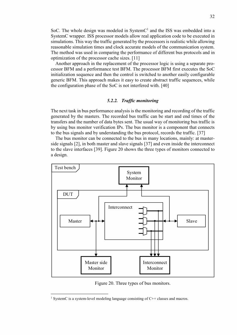
The bus monitor can be connected to the bus in many locations, mainly: at master-
side signals [2], in both master and slave signals [37] and even inside the interconnect
to the slave interfaces [39]. Figure 20 shows the three types of monitors connected to
a design.
Master side
Monitor
Master
Test bench
DUT
Interconnect
Monitor
System
Monitor
Interconnect
Slave
Figure 20. Three types of bus monitors.
1 SystemC is a system-level modeling language consisting of C++ classes and macros.

33
Master-side monitoring enables the measurement of such info as: time of bus request
to response from slave (round-trip latency) and the throughput achieved by the master
[2]. Slave-side monitors can be used in measuring the throughput of the interconnect
[39]. A bus monitor that connects to both the master and slave interfaces adds the
ability to measure the propagation delay of the request from master to slave or the
response from slave to master (end-to-end latency) [37].
Typically, the monitor decodes the transfer information from the bus signals at run-
time [37]. Another approach is making the bus monitor a component that records the
simulation time bus signal values into a file. An analyzer component can then be de-
veloped and used after the simulation to process the bus data into transfers, latencies
and throughput information. [2]
In order to increase the reusability and allow multiprotocol support the bus monitor
can be separated into multiple components. Tiwari A. et al. created a three-stage bus
monitor where the protocol dependent bus monitor (adapter) is connected to the
higher-level protocol independent bus monitor called performance monitor. The per-
formance monitor then contains one or multiple leaf monitors. The connection between
the adapter and the performance monitor is done via analysis port in UVM2 (Universal
Verification Methodology) in a class-based test environment. The role of the adapter
is to convert the bus traffic into so-called performance transactions. The performance
transactions contain such information as the start and end times of the transfers and
the number of data bytes transferred. The protocol independent performance monitor
then takes these performance transactions and passes them to the appropriate leaf mon-
itor. The leaf monitors are responsible for calculating and reporting the latency and
bandwidth. The leaf monitors also flag the transfers for violations based on the require-
ments set for different traffic patterns. Traffic with different requirements can be, for
example, processor load and store operations. By dividing the monitor into protocol
dependent and protocol independent parts, Tiwari A. et al. were able to use the perfor-
mance monitor with multiple bus protocols such as AHB, AXI and OCP. [37]
Larson K. et al. took a similar approach of multi-stage bus monitor. They verified
the performance of an AXI bus arbiter by using the Synopsys VMM2 (Verification
Methodology Manual) Performance Analyzer. An AXI port monitor was created and
the port monitors were connected to the master interfaces in VMM test bench. The
port monitors then tracked the interface signals, and reported the start and end times
of the transfers to the higher level VMM Performance Analyzer. [4]
Another monitoring component usually added into bus verification is the bus proto-
col checker [39]. A bus protocol checker makes sure that the bus traffic always adheres
to the bus protocol by monitoring the bus signals for violations. This is especially im-
portant if abstract traffic generator IPs are used instead of the real masters.
5.2.3. Data processing and reporting
The bus monitor provides the means for tapping into the bus interface and transforming
the bus traffic into a readable format. The typical parameters recorded are the start and
end times of the transfers and the relevant address and control information such as the
initiator, target address, read/write info and number of bytes transferred. The derived
2 UVM and VMM are standardized methodologies for building verification environments. They pro-
vide an extensive base class library written in SystemVerilog. The user generated verification clas-
ses can utilize these features by extending the base classes.

34
information reported can be latencies in clock cycles and the throughput. The mini-
mum, maximum and average latency and throughput are also typically calculated, as
well as arbitration latency for every master. The latency and throughput requirements
can be added to the report with the information, whether the requirements were met or
not. [37 and 4] The measurements can be divided into timing windows to study the
throughput variation in long simulations [2].
When the data is collected it can be stored into multiple files containing information
on every transfer or a summary of the simulation [37]. In some setups, even databases
such as SQL (Structured Query Language) have been used. This allows data to be
collected from multiple simulation runs. [4]
Many types of graphs can be used in visualizing the collected data. The typical
graphs used in the bus performance analysis are listed in Table 1.
Table 1. Typical performance analysis graphs.
Graph type Usage
Latency versus time Shows the variation of latency in time and whether
the latency requirements were met [2]
Throughput versus time Analysis of the bus throughput variation in time [2]
Arbitration latency
Average wait time of masters with for example dif-
ferent number of masters or different arbitration
schemes; describes system performance in differ-
ent traffic loads [26]
Countless graphing software exists to create these graphs, such as: Microsoft Excel,
OriginLab Origin, MathWorks MATLAB, gnuplot and GNU Octave. Even statistical
programs such as R have been used in processing the performance data [41].
5.3. Commercial EDA tools and verification IPs
The commercial EDA (Electronics Design Automation) tools for bus performance ver-
ification can be divided into two categories: verification IPs and performance suites.
This chapter provides a brief introduction to the commercial landscape of bus perfor-
mance verification. The information is based only on product briefs and marketing
material available online.
Many vendors, such as Cadence [42], Mentor [43], Synopsys [44] and Truechip [45]
provide bus master and slave verification IPs and also monitor IPs with performance
analysis capabilities. Some EDA tool makers also provide full bus performance veri-
fication suites, such as Cadence Interconnect Workbench, Sonics SonicsStudio and
Synopsys Platform Architect. The software suites mentioned are geared towards ar-
chitectural level design and optimization of complete SoCs or the interconnect struc-
tures. [46, 47 and 48]
Cadence Interconnect Workbench is a GUI (Graphical User Interface) -based soft-
ware for functional verification and performance analysis of SoC interconnects. The

35
software takes in an ARM CoreLink interconnect created with the ARM AMBA De-
signer software. In performance-oriented mode the software then integrates the inter-
connect into a UVM verification environment containing Cadence AMBA traffic gen-
erators and performance monitor verification IPs. The user is able to simulate and eval-
uate the performance of the interconnect with multiple traffic profiles and, for exam-
ple, plot the latencies and bandwidths in the GUI. [46 and 9]
Another commercial tool that includes bus performance analysis functionality is the
Sonics SonicsStudio. SonicsStudio is a total SoC development and verification envi-
ronment. It allows the designer to integrate their own IPs together with Sonics’ prod-
ucts via a GUI. In bus performance analysis, it provides static performance analysis as
well as RTL and SystemC simulations. Transfer latencies and bus bandwidths can be
viewed graphically and transactions can be traced and visualized in the GUI. [47]
Synopsys Platform Architect provides similar functionalities as SonicsStudio, with
GUI software and SystemC models. It allows early analysis and optimization of mul-
ticore SoCs, with such functions as bus transaction tracing and analysis, and hardware-
software performance validation. [48]

36
6. IMPLEMENTATION OF THE PERFORMANCE ANALYSIS
This chapter presents the implementation of the performance analysis tests. The veri-
fication IPs developed are introduced in Chapter 6.1. The structure of the test bench is
described in Chapter 6.2 and Chapter 6.3 shows how the bus traffic is modeled in the
tests.
6.1. AHB-Lite verification IPs
Multiple verification IPs were developed, in order to generate traffic for performance
tests and to monitor the bus signals. For monitoring, the AHB-Lite Monitor was de-
signed. The traffic generator used was an existing AHB-Lite master verification IP. In
order to simplify the configuration of the traffic generator master and the connection
to the design the AHB-Lite Agent was developed. It encloses the Monitor and master
IPs. The following chapters describe the developed verification IPs in detail.
6.1.1. AHB-Lite Monitor
The first verification IP developed was the AHB-Lite Monitor. It connects to the mas-
ter-side bus signals, records the traffic, and calculates the performance metrics. The
Monitor allows an automatic measurement of round-trip latency from master transfer
request to slave ready response. It also calculates and reports the average throughput
achieved, as well as other statistical information. The Monitor is most useful in per-
formance tests, but it can also be used as a tool to visualize and trace any AHB-Lite
master traffic in the design. It is not designed for functional verification as it does not
verify that the transfers are routed to the correct slaves. If this functionality would be
needed, a system-level monitor that connects to both the master and slave signals
would have to be designed. System-level monitor increases the connections needed to
the design and adds complexity.
The Monitor was written in SystemVerilog as a set of classes. It connects to the
design via a single SystemVerilog interface. A UML3 (Unified Modeling Language)
class diagram of the Monitor and the related classes is shown in Figure 21.
3 UML is an industry standard way of visualizing the structure, interaction and behavior of software
systems.

37
performanceMonitor
inbox < cl_PerformanceTransaction >
outbox < cl_PerformanceTransaction >
*
1
std::mailbox < T >
1
1
cl_PerformanceMonitor - masterName : string+ ta_printMailbox()
+ ta_mailboxToCsv()
cl_AHBLiteMonitor
- uin : in_AHBLite
- masterName : string
- monitoring : bit
- toggleStart : bit
- toggleEnd : bit
- cycleCountEven : int unsigned
- cycleCountOdd : int unsigned
- lastTransferIndicator : bit
- prevAddr : logic[31:0]
- waitedTransFlag : bit
- ta_captureEvenTransaction()
- ta_captureOddTransaction()
- fu_checkStartCondition(): void
- fu_checkEndCondition(): void
- fu_getTransfSize(): int unsigned
- fu_getTransfType(): string
+ ta_monitor()
+ ta_printMailbox()
+ ta_mailboxToCsv()
+ fu_stopMonitor(): void
cl_PerformanceTransaction
- startTime : time
- endTime : time
- latency : int unsigned
- addr : logic[31:0]
- wData : logic[DW-1:0]
- rData : logic[DW-1:0]
- rwType : string
- size : int unsigned
+ toString(): string
+ toCsvString(): string
1
Figure 21. Class diagram of the developed AHB-Lite monitor IP.
As can be seen in Figure 21, a two-stage approach was taken for the Monitor. The
Monitor consists of two classes, the cl_AHBLiteMonitor and cl_PerformanceMonitor.
The cl_AHBLiteMonitor functions as an adapter and translates the bus activity into
higher abstraction level. The information is then taken in and processed by the cl_Per-
formanceMonitor. This approach tries to maximize reusability and the cl_Perfor-
manceMonitor can be used with all parallel bus protocols, not just with the AHB-Lite.
The cl_AHBLiteMonitor is a class that connects to the master signals via the uin
interface. At every bus clock cycle, it checks the bus signals for the transfer start and
end conditions. This information is then used by the two tasks, ta_captureEvenTrans-
action() and ta_captureOddTransaction(), running on separate threads. The AHB-Lite
protocol can have two transfers active at the same time so this approach allows the
Monitor to record the latencies of every individual transfer accurately, with any trans-
fer type. After a transfer is recorded, it is packaged into a class format called cl_Per-
formanceTransaction and put into a standard library mailbox object, named outbox.
After the simulation, when all transfers are done and the data has been collected into
the mailbox, the results can be printed into text files by calling the ta_printMailbox()
task in the cl_AHBLiteMonitor. This task invokes the similarly named task in the
cl_PerformanceMonitor. In cl_PerformanceMonitor the information is taken from the
mailbox, formatted appropriately and printed into text files. Statistical information
about latency and throughput is also calculated and reported. Figure 22 shows an ex-
ample result file.

38
Summary file is also created, which contains only the statistical information about
the masters. This enables quick checks that the latency and throughput values of the
masters are not violating the requirements. If violations are seen, the full result file can
be used for checking the detailed information about the exact slow transfers. The
timestamps of the transfers can then be checked in the simulation waveform to further
investigate the situation.
Another type of file that can be generated with the Monitor is a comma-separated
text file. This file contains the same transfer-based information as the previously dis-
cussed result file, but with simpler, comma separated formatting. This makes it easy
to develop additional scripts that can be used for data processing and graphing.
6.1.2. AHB-Lite Agent
In order to generate bus traffic for the performance tests, an existing AHB-Lite master
verification IP is used. The master verification IP acts as a traffic generator and gives
total flexibility to create any type of traffic. Because many traffic generators and mon-
itors are needed in the test bench, the master IP and the Monitor were wrapped into
one class called AHB-Lite Agent. Figure 23 shows the structure of the Agent.
AHB-Lite master IP SVI
AHB-Lite Monitor
AHB-Lite Agent
ta_run()
ta_stop()
appendTransaction(type)
printResults()
DUT
Figure 23. AHB-Lite Agent.
The Agent is a SystemVerilog class with one SystemVerilog interface (SVI) for the
master IP and Monitor. The Agent also contains tasks that make loading the master IP
with AHB-Lite transactions easy.
AHB Example master
START TIME | END TIME | LATENCY | READ/WRITE | TARGET | SIZE (BYTES) | DATA
125 | 135 | 2 | READ | 00000000 | 4 |168bc342
135 | 145 | 2 | READ | 00000000 | 4 |168bc342
...
665 | 695 | 4 | WRITE | 00002000 | 4 |c5362c04
Transfer count | 30
Total time (ns) | 570
Avg latency (cycles) | 3
Min latency (cycles) | 2
Max latency (cycles) | 4
Avg throughput (Mbps) | 6737
Figure 22. Example result file generated by the Monitor.

39
6.1.3. Validating the verification IPs
The functionality of the Agent and Monitor was validated in multiple scenarios. The
testing of the Agent started with one Agent connected to an existing AHB-Lite slave
verification IP with a SystemVerilog interface (SVI). The AHB-Lite master IP inside
the Agent was configured to execute multiple different traffic patterns, and the validity
of the information in the Monitor’s output text file was analyzed. The validation of the
latency results was done by configuring the slave to output the number of wait cycles
of the transfers into a text file. In a single slave - single master situation the slave wait
states correspond to the amount of additional latency seen by the master. The test
bench is shown in Figure 24.
AHB-Lite Agent SVI AHB-Lite Slave
latenciesRX wait
TX wait
comparison
Figure 24. Validating the AHB-Lite Agent latency measurement.
Another test done with the setup in Figure 24 was the Monitor’s functionality in the
slave error response (HRESP) situation. The Monitor reports this as a simulation error
in the simulation log file.
The problem with the setup in Figure 24 is that it cannot automatically verify laten-
cies of pipelined waited transfers. This is because in waited transfers the ongoing trans-
fer delays the next transfer by extending its address phase. The latency of the transfers
does not then match directly with the slave wait states.
In order to test the Agent’s functionality in a more realistic scenario a test bench was
created with one Agent connected to an AHB-Lite multi-layer interconnect and two
slave verification IPs. The Agent was configured with a sequence of pipelined and
separated reads, writes and idle transfers to different addresses and slaves. Simulation
was run until the Monitor’s code coverage (statement, branch and conditional cover-
age) was 100 %. Monitor’s output file was then verified to match with the designed
transfer sequence. The results in the output file were also compared to the simulation
waveform to make sure that the reported latency and other transfer information were
correct. Later longer, more randomized sequences, were successfully tested with this
setup. Further development work would be needed to automate this validation process,
but for now, the tests of the Agent were deemed sufficient.
As the Monitor can also be used as a separate verification IP, its functionality was
checked also with the processor simulation model. An existing test case was taken,
and the Monitor was connected to the processor’s master bus. Again, output files and
waveforms were extensively compared in order to make sure that the Monitor supports
all of the processor’s transfer types. This validation method builds confidence in the
Monitor’s functionality in various use cases.

40
6.2. Test bench
The test bench created for the performance tests contains the whole modem design
with the Agents replacing the functionality of the design AHB-Lite masters. The
Agents were connected to the bus signals via the SystemVerilog interfaces. The Sys-
temVerilog interfaces enable the abstract class based verification IPs to be connected
to the RTL of the design. No design RTL changes are needed and the hierarchical bus
connections are parametrized for easy manipulation. This allows fast performance val-
idation after any bus related design update. Figure 25 shows the structure of the test
bench.
Agent 0
Protocol
Checker
Sequencer
InterconnectMaster 0
Slave
Master 1
Protocol
Checker
Agent 1
Test bench
Modem
transactionstransactions
Figure 25. Simulation environment for bus performance tests.
Figure 25 shows that for every design master two components are instantiated in the
test bench: the Agent and a protocol checker. The Agent takes over the bus signals and
replaces the design master. An AHB-Lite protocol checker IP is added in order to safe-
guard the bus traffic.
A class-based verification IP called Sequencer was also developed. The Sequencer
contains all the test case traffic sequences. It contains tasks that load the Agents with
read, write and idle transfers. SystemVerilog’s randomization is used in creating cer-
tain variation in the traffic patterns, especially in the delays between transactions.
When new test sequences are created, they can simply be added to the Sequencer class
as a task.

41
The test bench also contains a task for result file handling. The task calls the print
methods of the Agents one by one and collects the master traffic results into text files.
Special care was taken not to break the ability of the processor simulation model to
configure the modem in the beginning of the simulation. For this reason, the test pro-
gram contains an initial configuration phase where the processor bus is open for the
processor model. After the configuration phase, the processor model is disabled and
the bus control is given to the Agent connected to the processor’s bus.
6.3. Traffic pattern generation
As discussed previously, the performance tests can contain many arbitrary tests, such
as maximum read and write tests with back-to-back transactions. However, many fac-
tors defining the bus performance come from the type of bus traffic generated by the
masters and the congestion of the interconnects. This is especially true for arbitration
latency. It was shown previously in Equation 3 in Chapter 4.2.2 that the arbitration
latency depends exponentially from channel utilization ratio (CUR). Therefore, in or-
der to measure the arbitration latency accurately, the bus traffic must be modeled real-
istically.
Realistic bus traffic in the tests was modeled in multiple ways. The idea was to im-
itate the maximum bus activity of each master. For some DMA devices, this means
simply doing periodic reads and writes with the expected maximum throughputs. For
complex hardware accelerators, the activity was divided into communication intensive
and computation intensive parts. IP-level simulations were run, and the waveforms
studied. The parts of the simulations, where the bus utilization is the highest for a
reasonable amount of time, were chosen. The selected transfer sequences with the ex-
act delays were then reproduced and configured into the corresponding Agents.
The traffic of the processor was imitated by doing periodic “instruction” and “data”
accesses to the memory. In addition to these, the processor Agent was configured to
access selected peripherals in order to measure the peripheral access latencies in a re-
alistic crowded bus situation.
Multiple test cases were developed, such as ones imitating uplink and downlink data
transmissions. The transfer addresses of the Agents were chosen to match the scenar-
ios, in order to model the operation realistically. An example traffic pattern of selected
masters is shown in Figure 26.

42
Figure 26. Traffic pattern recorded in a normal simulation showing accesses to two
slaves (red and cyan).
The colors in Figure 26 represent the different slaves and the width of the boxes
show the transfer times from master request to slave response. Master 1 seems to be
experiencing quite long transfer times compared to the other masters. In order to model
the “bursty” or intermittent traffic of the real masters, randomized idle times were
added to the traffic patterns of the Agents. Figure 27 shows a snapshot from this kind
of simulation.
Figure 27. Modeling intermittent traffic.
In Figure 27 it can be seen that the transfer times of master 1 are considerably shorter
when other masters are quiet. The idle durations chosen are few hundred clock cycles

43
and their interval is between about every fifty transfers. The values were chosen arbi-
trarily and they do not necessarily match the operation of the real masters. Similar
approach of randomized idle periods was taken in [28].

44
7. PERFORMANCE ANALYSIS RESULTS
This chapter presents the simulated latency and throughput results. Firstly, in Chapters
7.1 and 7.2 the selected results from the downlink tests are shown and discussed. Then,
in Chapter 7.3 the traffic patterns are modified by adding random idle periods and the
results presented. Finally, the summary of the uplink test results is shown in Chapter
7.4. The graphs presented in the chapters are generated with GNU Octave scripts from
the comma-separated text files created by the AHB-Lite Monitors.
7.1. Latency
The processor’s latency graph can be seen in Figure 28. In this test, the processor is
configured to access four different peripherals (slaves 1-4) and the transfer latencies
are measured. During the simulation, other masters are active and operating at the ex-
pected maximum throughput. However, they are not accessing these four peripherals
so the processor has an uncontested access to the slaves 1-4.
Figure 28. Processor’s transfer latencies to peripherals (normalized).
In Figure 28 it can be seen that the transfer latencies vary between different periph-
erals. The read (circle) and write (square) latencies of some peripherals also differ with
write latencies being usually slightly higher.

45
From this measurement, it was deemed that the latency to the slave 3 (blue) is too
high and a modification to the bus structure must be made, in order to improve perfor-
mance. The latency sources from the processor to the slave 3 were analyzed, and the
highest contributor to the latency was found out to be the master and slave clock speed
difference. Originally, the processor master interface and the peripheral slave interface
had an 8:1 clock speed ratio. The slave interface clock speed was raised, and also the
now unneeded synchronizer bridge removed. After the update, the master and slave
bus clock speeds have a 2:1 ratio. The results after the performance update can be seen
in Figure 29.
Figure 29. Processor’s transfer latencies after an update to the slave 3.
The higher clock speed at the slave-side causes a big drop in the transfer latencies
to the slave 3 (blue). The average latency from the processor to the slave 3 has dropped
to one fifth of the original latency, and is now at an acceptable level.
Figure 30 shows the average latencies of all masters in the downlink simulation.
Two simulations were made with the same transfer sequences configured to the Agents
in both simulations. In the first simulation, the Agents operate individually. The first
Agent runs its sequence, stops, and the turn is given to the next Agent. This sets a
baseline on the latencies of the bus structure and the slave delays, because no compe-
tition between the masters happens. The second simulation is the more realistic case
where all relevant masters are operational.

46
Figure 30. Average latencies in two tests (normalized, downlink).
In Figure 30 it can be seen that the latencies of masters are quite diverse, ranging
from 0.05 to 1.0. The error bars represent the uncertainty of reported results. Most
masters are not greatly affected by the contentions at the slaves, but couple of masters
really stand out: master 1 and master 3. Master 9 also shows a measurable difference
in the average latency. Master 1’s latency is 10 times higher in the crowded simulation
compared to the single master simulation. This is the absolute worst-case scenario,
with continuous traffic, with the highest activity recorded in the IP-level simulations.
7.2. Throughput
Figure 31 shows the windowed throughput of a hardware accelerator accessing single
memory in two test cases. The window size chosen is 10 transfers. As previously, the
two tests done are: one where other masters are quiet and only this hardware acceler-
ator is active, and a second one where all the relevant masters are active and competing
for the same memory resources. Single master test gives a baseline on the throughput
to the memory with the configured traffic pattern.

47
Figure 31. Throughput of a hardware accelerator in two test tests (normalized).
A 14 % decrease in average throughput can be seen due to other masters competing
for the bus. At the same time this means a 15 % increase in the total transfer time of
210 transfers. All of the masters were configured to operate at the highest expected
throughput, which is much higher than the extended average throughput in the real
operation. The tests do not try to mimic the “bursty” operation of the real masters.
Figure 31 demonstrates the effect of arbitration and slave congestion at the expected
worst-case scenario.
Figure 32 shows the average throughput of the masters. The results are from the
same simulation runs as the latency results shown in Figure 30.

48
Figure 32. Average throughput of masters in two tests (normalized, downlink).
Masters 1 and 3 show a significant drop in the average throughput due to traffic
from other masters blocking the bus. The average throughput of master 1 is approxi-
mately five times higher in the single master simulation. This means an 81 % decrease
in average throughput due to bus congestion. Masters 9 and 10 also show small
throughput changes. Other masters do not experience any major change in the average
throughput. This test shows that there is a possibility for a big drop in master 1 and 3
throughput due to competition.
From the latency results in Figure 30 and the throughput results in Figure 32 couple
of things can be deduced. For most of the masters, the extreme traffic from the other
masters causes no significant performance drop. Performance of these masters cannot
be enhanced by altering the arbitration scheme. The only way to increase throughput
and decrease transfer latencies is to modify the bus structure (remove synchronizers,
increase clock speeds, etc.) or to modify the slaves to lower the slave access times.
On the other hand, for some masters, most notably masters 1 and 3, performance
gains can be achieved by modifying the arbitration or the bus structure in order to
allow fairer access to the slaves. Careful analysis must be done to make sure that the
bus access pattern of the masters is such, that some low traffic time is left for these
two masters to access the slaves.

49
7.3. Intermittent traffic
The same downlink test is done with modified traffic sequences, with quiet periods
added here and there as shown in Chapter 6.3 in Figure 27. The quiet times try to
imitate the “bursty” behavior of the real masters. Figure 33 shows the latency results
from this simulation.
Figure 33. Average latencies with intermittent traffic (normalized to match Figure 28,
downlink).
Master 1 is still showing slightly higher latencies when all masters are active. Still,
this is not anything major and all masters have practically the same average transfer
latencies in both cases. Figure 34 shows the throughput results.

50
Figure 34. Average throughputs with intermittent traffic (normalized to match Figure
31, downlink).
The throughput drops of masters 1 and 3 in the crowded simulation are almost gone.
Masters 1, 3, 9 and 10 are transferring to the same memory and with this intermittent
traffic, all four masters are able to operate without much interaction. The intermittent
traffic test shows that with the possibly more realistic traffic patterns, the masters are
able to catch up in the low traffic times of others. None of the masters experience any
significant slowdown.
7.4. Uplink test results
In order to analyze the system-level bus performance in the uplink communication
case, similar simulations as previously shown are done. The uplink scenario is inter-
esting because it contains some different masters, memories and traffic patterns. The
summary of results is shown and briefly discussed. The average latencies in uplink
simulation are shown in Figure 35.

51
Figure 35. Average latencies in two tests (normalized, uplink).
As can be seen in Figure 35 the masters 4, 5 and 7 are not needed in the uplink
processing, and the masters 14-17 are added. Again, as in the downlink test, masters 1
and 3 endure a big latency increase due to bus congestion. Other masters are not expe-
riencing latency increase. Figure 36 shows the throughput results from the same sim-
ulation.
Figure 36. Average throughput of the masters in two tests (normalized, uplink).

52
Masters 1, 3 and 15 show throughput drop but others are not affected. From the
uplink tests, it is possible to say that these three masters should be carefully analyzed
to verify that they meet the throughput requirements in all situations.

53
8. DISCUSSION
The goal of this thesis work was to create a simulation environment that is able to
model the realistic bus traffic inside a modem SoC and measure the latencies and
throughputs of the masters. The work was done in order to find the weak points of the
bus structure. The results show that the created simulation environment possesses the
required capabilities. With easy configurability of new tests and script based graphing
of latency, throughput and traffic patterns the environment has good potential for re-
use.
By using the object-oriented design methodology, the usage of the verification IPs
(Agent and Monitor) is straightforward. The functionality is abstracted inside the clas-
ses and a simple to use interface with couple of tasks is provided for the user. The
SystemVerilog interface makes the bus connections to the design easy. A two-stage
coding approach of separate protocol dependent bus adapter (cl_AHBLiteMonitor) and
performance monitor (cl_PerformanceMonitor) was taken with the Monitor verifica-
tion IP. This has been shown to produce highly reusable components that enable the
usage with multiple different bus protocols [37].
The unique feature of the simulation environment is the ability to show the relation
of communication performance between masters. The architectural level performance
analysis of the bus structure is no longer enough. The complexity of SoCs increases
and the processing gets more and more distributed and heterogeneous. Performance
validation through simulation is getting more relevant as demonstrated also in [1] and
[37].
The current simulation environment does not model the dynamic interaction be-
tween masters. This creates a severe limitation on the verification capabilities. Cur-
rently, the only results that can be obtained are for the worst-case performance, where
all masters are operational at the same time. Of course, the sequence of master activity
could be modeled more accurately. That said, this kind of modeling is extremely dif-
ficult. A deep knowledge of the modem operation would be needed. For this reason,
the simulations concentrate on the worst-case performance where all masters are op-
erational simultaneously.
A more realistic approach would be to simulate the whole design with real, func-
tional traffic. This was done by Loghi M. et al. for a multi-processor SoC by replacing
the design masters with processor instruction set simulators. Real application code was
then executed with the processors, and the performance of the system-level bus ana-
lyzed. [11] The same approach cannot be taken with the studied modem because it has
many hardware accelerators besides the processor. Configuring the modem and run-
ning it in the simulation with the real masters in data communication mode is currently
unrealistic. The simulation times would be too long. Possible workaround would be to
use an FPGA (Field Programmable Gate Array) or an emulation platform to speed up
the runtimes. However, the usage of such devices severely limits the ability to trace
and visualize the bus signals deep down in the design hierarchy at clock cycle level.
Lehongre D. et al. analyzed the system-level bus performance of a complex multime-
dia SoC via emulation. They created synthesizable adapters that monitor the bus sig-
nals and convert the activity into transaction information. The transaction information
was then, after the simulation, dumped from the adapter memories to a file and ana-
lyzed. [49] Similar approach could possibly be taken with the modem, if deeper anal-
ysis is needed.

54
The results in this thesis show that most masters do not experience any significant
latency increase or throughput decrease due to bus congestion. The communication
performance of these masters is not dependent on the operation of other masters. The
exceptions are masters 1, 3, and in the uplink tests, master 15. From the results it can
be concluded that any design effort to enhance the arbitration scheme, or in general
the fairness of bus access, should be pointed at the interconnects serving these three
masters.
The measured throughput values in the crowded bus simulations give a good esti-
mate on the absolute worst-case performance. The values can be analyzed to under-
stand whether the system performs as required. The performance overhead can also be
calculated. The communication requirements of a modem relate to the required data
throughput. In practice, however, the accurate analysis of the exact throughput and
latency requirements is quite complicated. Depending on the implementation, some
DMA overhead exists. This overhead should then be calculated and added on top of
the required data throughput.
The most valuable results from this thesis were the ones that led to immediate action.
The processor transfer latencies were deemed critical and the measurements revealed
multiple master-slave channels that were not performing as expected. Optimizations,
such as the clock speed raise of a peripheral as shown in the results were made and the
updates were verified to be successful with the simulation environment. The simula-
tions do not reveal the individual latency sources. Only the total latency is reported.
From the results, the individual latency sources have to be manually analyzed and cat-
egorized as shown in the theory part of this thesis. Lastly, the results provide peace of
mind that the parallelism works as expected and most bus channels are extremely fast
and predictable: never showing signs of slowdown.
The main future use for the environment is the validation of performance updates.
When the bus structure is modified, a fast simulation shows how the performance is
affected. In theory, the simulation environment, and more specifically the Agent IPs,
could be used at the verification of the whole bus structure. Early on in the chip design,
the bus structure could be created with shell masters and slaves. The Agents would be
connected to the master interfaces and slave verification IPs at the slave interfaces.
The performance of the bus structure could then be measured with similar simulations
as presented in this thesis. This would allow the decisions on the arbitration schemes
and the bus topology to be made and the performance verified from the get go. There
are commercial tools, such as the Cadence Interconnect Workbench, which are built
exactly for this purpose [46].
A future use for the Monitor IP is that it can be connected to any master-side bus
signals to monitor and report the bus activity. This allows an easy way to visualize the
transfer-level bus traffic. It can also enable any simulation to record bus performance
data. This might help uncover some unexpected weak points in the bus structure.
There is a huge temptation to do updates to the bus structure that seem to improve
the performance. The time spent on doing the optimization is worth it if the update
leads to a simpler bus structure, reduces power consumption or improves the perfor-
mance measurably. If the goal is for example to reduce master’s transfer latencies to
some slave, the results are easy to validate with simple pre-update and post-update
simulations. These simulations can be done without the performance analysis environ-
ment presented in the thesis. However, it gets more difficult if the goal is to reduce the
bus congestion or to relieve the strain on some interconnect. The validation of the need
for an update, and finally the effectiveness of the update done is impossible in simple

55
functional simulations. This is where the created simulation environment is most use-
ful.
56
9. SUMMARY
This thesis is a study of the system-level bus performance in a modem SoC. The re-
quirements of the SoCs internal communication are studied and the main causes lim-
iting the performance presented. The created simulation environment is able to model
the modem bus traffic and provide insight into the possible bottlenecks of the bus
structure.
The data processing done in the modem contains many processing phases, such as
encryption, coding and modulation. Modem has hard real-time constraints on the pro-
cessing times and requirements for throughput. For this reason, the importance of high
performance communication structure inside the chip is extremely important. The la-
tencies of individual transfers are typically not that crucial. An exception is the real-
time needs of a processor interrupt. Long transfer times also increase the power con-
sumption if they make the transferring master unable to enter sleep state. Throughput
is crucial, and the communication structure must be able to provide the varying
throughput needs of the data processing phases.
The parallel bus is the common means for system-level communication in an SoC.
The modem uses the common parallel bus interface ARM AMBA 3 AHB-Lite. The
system-level bus structure consists of multiple ARM multi-layer AHB interconnects.
The interconnects allow the address mapped transfers to be routed correctly between
the masters and slaves. Interconnects also have the important task of deciding which
masters get the turn to transfer first. This is called arbitration. There are multiple arbi-
tration schemes, of which, the most common ones are the static priority, round-robin
and TDMA. Many variations of these strategies exist, such as the programmable pri-
ority based arbitration scheme used in the studied modem. The static priority is the
simplest arbitration scheme but it leaves a possibility for a bus master to not be served
for a long time, possibly leading to starvation. Round-robin allows a fair access and
the masters are served in circular order. It gives good performance and predictability
when the masters have the same bandwidth needs. The advantage of TDMA is the
extremely predictable timing of the transfer frames. It can use the bandwidth ineffi-
ciently.
The system-level bus performance can be characterized by two concepts: bandwidth
and latency. The efficient bandwidth or throughput can be increased by making the
data bus wider, increasing the bus clock speed or reducing computation or communi-
cation latencies. The bus transfer latency is characterized by the bus protocol, the ar-
bitration, the delay elements between the master and slave and the memory access
times. Arbitration latency is the most unpredictable latency source in the system-level
bus, caused by multiple masters competing for slave accesses.
The simulation-based system-level bus performance analysis can be divided into
three stages: traffic generation, traffic monitoring and data processing. The bus master
operation is typically modeled, for their ease of configurability, using class based traf-
fic generator verification IPs. Bus can be monitored from the master-side, slave-side
or both. Again, class-based verification IPs are common. Typical reports and graphs
include the transfer latencies and throughputs of the masters with statistical infor-
mation such as simulation averages.
An RTL simulation environment was created and used in measuring the throughputs
and latencies of the masters in the modem. The created environment contains the test
bench as well as multiple AHB-Lite Agents modeling the real masters. The simulations
include tests that model uplink and downlink bus traffic at the worst-case situation,

57
where all masters are active simultaneously. The traffic is modeled by copying the
traffic patterns from the individual IP-level simulations. Small variations are added as
well as some quiet times in order to better model the computation and communication
intensive parts of the master operation.
The simulation results show that most masters are able to operate without much
intervention. Nevertheless, there are optimizations to be made. The processor latency
to some peripheral slaves was concluded to be too high. The clock speed of slave bus
was increased, and after the optimizations the latency dropped to an acceptable level
of one fifth of the original. The simulation results also show that the master 1 is heavily
influenced by bus congestion. At worst case, master 1 experiences an 81 % decrease
in average throughput compared to the single master situation. Masters 3 and 15 also
experience a measurable throughput drop. Quiet times were configured to the masters,
in order to model more realistically the overall bus traffic. The bus congestion is much
lesser and the throughput drop of the masters is almost nonexistent. The simulation
environment was able to show some known weak points in the bus structure, as well
as uncover couple of new places ripe for performance optimizations.

58
10. REFERENCES
[1] Pasricha S. & Dutt N. (2008) On-Chip Communication Architectures: System
on Chip Interconnect. Morgan Kaufmann, Burlington, 521 p.
[2] Pelissier G., Hersemeule R., Gambon G., Torres L. & Robert M. (2001) Bus
analysis and performance evaluation on a SOC platform at the system level de-
sign. In: VLSI-SOC 11th International Conference on Very Large Scale Integra-
tion, December 3-5, Montpellier, France.
[3] Palkovic M., Raghavan P., Li M., Dejonghe A., Van der Perre L. & Catthoor F.
(2010) Future Software-Defined Radio Platforms and Mapping Flows. IEEE
Signal Processing Magazine 27, p. 22-33.
[4] Larson K., Dickol J. & O'brian K. (2010) Performance verification of a complex
bus arbiter using the VMM Performance Analyzer. EE Times, MediaTek Wire-
less, Inc.
[5] Kuiper G. (2013) Guaranteed-Throughput Improvement Techniques for Con-
nectionless Ring Networks. Master’s Thesis. University of Twente, Department
of EEMCS, Enschede.
[6] Lavagno L., Martin G., Markov I. & Scheffer L. (2016) Electronic Design Au-
tomation for IC System Design, Verification, and Testing. Taylor & Francis
Group, Boca Raton, 644 p.
[7] Nilsson A. (2007) Design of programmable multi-standard baseband processors.
Doctoral dissertation. Linköping University, Department of Electrical Engineer-
ing, Linköping.
[8] Ecco L., Saidi S., Kostrzewa A. & Ernst R. (2015) Real-time DRAM throughput
guarantees for latency sensitive mixed QoS MPSoCs. In: 10th IEEE Interna-
tional Symposium on Industrial Embedded Systems (SIES), European Union.
[9] Heaton N. (accessed: October 19th 2016) How to Measure and Optimize the Sys-
tem Performance of a Smartphone RTL Design. ARM Connected Community,
Cadence. URL: https://community.arm.com/groups/soc-implementa-
tion/blog/2013/10/29/how-to-measure-and-optimize-the-system-performance-
of-a-smartphone-rtl-design.
[10] Application note: Atmel AVR1304: Using the XMEGA DMA Controller
(2013). Atmel, San Jose, 11 p.
[11] Loghi M., Angiolini F., Bertozzi D., Benini L. & Zafalon R. (2004) Analyzing
On-Chip Communication in a MPSoC Environment. In: IEEE Proceedings of
the Design, Automation and Test in Europe Conference and Exhibition, Febru-
ary 11-14. Vol. 2, p. 752-757, Italy.

59
[12] Pahlavan K. & Krishnamurthy P. (2009) Networking Fundamentals: Wide, Lo-
cal and Personal Area Communications. John Wiley & Sons Ltd, Chichester,
656 p.
[13] IEEE standard 802.11a supplement: Wireless LAN Medium Access Control
(MAC) and Physical Layer (PHY) Specifications. High-speed Physical Layer in
the 5 GHz Band (1999). IEEE, New York, 90p.
[14] Ayla J. (2011). Communication Architectures for Systems-on-Chip. Taylor &
Francis Group, Boca Raton, 402 p.
[15] Specification: AMBA 3 AHB-Lite Protocol v1.0 (2006). ARM, 72 p.
[16] Overview: Multi-layer AHB (2004). ARM, 8 p.
[17] Jerraya A. & Wolf W. (2005) Multiprocessor Systems-on-chips. Morgan
Kaufmann, San Francisco, 581 p.
[18] Shin E., Mooney J. & Riley G. (2002) Round-robin arbiter design and genera-
tion. In: IEEE 15th International Symposium on System Synthesis, October 2-4,
Kyoto, Japan, p. 243-248.
[19] Sonntag S. & Helmut R. (2008) An Efficient Weighted-Round-Robin Algorithm
for Multiprocessor Architectures. In: IEEE 41st Annual Simulation Symposium,
April 13-16, Ottawa, Canada, p. 193-199.
[20] Cilku B., Crespo A., Puschner P., Coronel J. & Peiro S. (2015) A TDMA-Based
Arbitration Scheme for Mixed-Criticality Multicore Platforms. In: IEEE First
International Conference on Event-Based Control, Communication, and Signal
Processing, June 17-19, Krakow, Poland, p. 1-6.
[21] Poletti, F., Bertozzi, D., Benini L. & Bogliolo A. (2003) Performance Analysis
of Arbitration Policies for SoC Communication Architectures. Design Automa-
tion for Embedded Systems 8, p. 189-210.
[22] Hwang S., Kang D., Park H. & Jhang K. (2010) Implementation of a Self-Moti-
vated Arbitration Scheme for the Multilayer AHB. IEEE Transactions on Very
Large Scale Integration (VLSI) Systems 18, p. 818-830.
[23] Patterson D. (2011) Computer Architecture: A Quantitative Approach. Morgan
Kaufmann, 856 p.
[24] Kyoungrok C., Hyeon-Seok N., Tae W. & Younggap Y. (2012) Analysis of sys-
tem bus on SoC platform using TSV interconnection. In: IEEE 4th Asia Sympo-
sium on Quality Electronic Design (ASQED), July 10-11, Penang, Malaysia, p.
227-231.
[25] Kim N-J. & Lee H-J. (2004) Design of AMBA TM Wrappers for Multiple-Clock
Operations. In: IEEE International Conference on Communications, Circuits and
Systems, June 27-29, p. 1438-1442.

60
[26] Suh J. & Yoo H-J (2004) Arbitration Latency Analysis of the Shared Channel
Architecture for High Performance Multi-Master SoC. In: IEEE Proceedings of
2004 IEEE Asia-Pacific Conference on Advanced System Integrated Circuits,
August 5-5, p. 388-391.
[27] Cho Y-S., Choi E-J. & Cho K-R. (2006) Modeling and Analysis of the System
Bus Latency on the SoC Platform. In: ACM SLIP '06: Proceedings of the 2006
international workshop on System-level interconnect prediction, March 04-05,
Munich, Germany, p. 67-74.
[28] Conti M., Caldari M. & Orcioni S. (2004) Performance analysis of different ar-
bitration algorithms of the AMBA AHB bus. In: IEEE Proceedings. 41st Design
Automation Conference, July 07-11, San Diego, USA, p. 618-621.
[29] White Paper: Everything You Wanted to Know About SOC Memory. (2011)
Tensilica, 29 p.
[30] Anendhar A. & Srilatha C. (2014) Implementation Methodology of High Perfor-
mance Multi Byte Data Access Control of AMBA Bus. International Journal of
Emerging Technology and Advanced Engineering 4, p. 461-465.
[31] Xu Y., Hu J., Xiao J., Yang G. & Kong W. (2016) Design Techniques for a 30-
ns Access Time 1.5-V 200K-bytes Embedded EEPROM Memory. IEEE Trans-
actions on Circuits and Systems II: Express Briefs 63, p. 1064-1068.
[32] Richter D. (2014) Flash Memories: Economic Principles of Performance, Cost
and Reliability Optimization. Springer Science & Business Media, Dordrecht,
268 p.
[33] Technical Reference Manual. AMBA Design Kit. Revision: r3p0 (2007). ARM,
226 p.
[34] Chelcea T., Nowick S. M. (2001) Robust Interfaces for Mixed-Timing Systems.
In: IEEE Proceedings of the 38th Design Automation Conference, June 22-22,
Las Vegas, USA, p. 21-26.
[35] Mishra S., Kumar Singh N. & Rousseau V. (2015) System on Chip Interfaces
for Low Power Design. Morgan Kaufmann, 406 p.
[36] Lahiri K., Ragunathan A. & Dey S. (2001) Evaluation of the traffic-performance
characteristics of system-on-chip communication architectures. In: IEEE Four-
teenth International Conference on VLSI Design, January 07-07, Bangalore, In-
dia, p. 29-35
[37] Tiwari A., Patel B., Patel J. & Modi K. (2015) Using a Generic Plug and Play
Performance Monitor for SoC Verification. In: Design and Verification
Conference and Exhibition, Austin, USA.

61
[38] Lahiri K., Raghunathan A, & Dey S. (1999) Fast Performance Analysis of Bus-
Based System-On-Chip Communication. In: IEEE/ACM International Confer-
ence on Computer-Aided Design. Digest of Technical Papers, November 07-11,
San Jose, USA, p. 566-572.
[39] Hwang S. Y., Kang D. S., Park H. J. & Jhang K. S. (2010) Implementation of a
Self-Motivated Arbitration Scheme for the Multilayer AHB Busmatrix. IEEE
Transactions on Very Large Scale Integration (VLSI) Systems 18, p. 818-830.
[40] Wen H., Chen J. & Huang D. (2013) Whitepaper: Tackling Verification Chal-
lenges with Interconnect Validation Tool. Cadence.
[41] Keppler B. & Jonack R. (2012) Presentation: SoC performance evaluation using
high performance SystemQ and TLM models for communications SoCs. Lantiq
Germany GmbH & Sonics Inc.
[42] AMBA AHB Simulation VIP Datasheet. (Accessed: October 20th 2016) Ca-
dence. URL: http://ip.cadence.com/ipportfolio/verification-ip/simulation-
vip/arm-amba/amba-ahb-simulation-vip.
[43] Mentor Graphics AXI Verification IP Suite (Altera Edition). (Accessed: October
20th 2016) Mentor® Verification IP Altera® Edition AMBA AXI3TM/AXI4TM
User Guide. URL: https://www.altera.com/products/intellectual-prop-
erty/ip/basic-functions/m-mentor-graphics-axi-verification.html.
[44] VIP Experts. (Accessed: October 20th 2016) How do you Verify the AMBA Sys-
tem Level Environment? VIP Central blog. URL: https://blogs.synop-
sys.com/vip-central/2015/03/19/how-do-you-verify-the-amba-system-level-en-
vironment/.
[45] Truechip's Products. (Accessed: October 20th 2016) AMBA 3 AHB-Lite Verifi-
cation IP. Truechip. URL: http://www.truechip.net/AMBA-AHB3-VIP.html.
[46] Goering R. (Accessed: October 19th 2016) Interconnect Workbench Eases Anal-
ysis and Verification for ARM-Based SoCs. Industry Insight Blogs. Cadence
Design Systems, Inc. URL: https://community.cadence.com/ca-
dence_blogs_8/b/ii/archive/2012/10/09/interconnect-workbench-eases-analy-
sis-and-verification-for-arm-based-socs.
[47] Sonics, Inc. (Accessed: October 19th 2016) SonicsStudio Director Product Brief.
Sonics, Inc. URL: http://sonicsinc.com/products/development-tools/sonicsstu-
dio-director/
[48] Synopsys. (Accessed: October 19th 2016) Platform Architect. PROTOTYPING
- ARCHITECTURE DESIGN. URL: https://www.synopsys.com/Prototyp-
ing/ArchitectureDesign/pages/platform-architect.aspx.
[49] Lehongre D. (Accessed: November 28th 2016) SoC interconnect performance
verification methodology based on hardware emulator. Design & Reuse.

62
STMicroelectronics. URL: http://www.design-reuse.com/articles/16220/soc-in-
terconnect-performance-verification-methodology-based-on-hardware-emula-
tor.html.